Precision Analog Microcontroller 12-bit Analog I/O ... · Precision Analog Microcontroller 12-bit...
78
Precision Analog Microcontroller 12-bit Analog I/O, ARM7TDMI® MCU Preliminary Technical Data ADuC702x Series FEATURES Analog I/O Multi-Channel, 12-bit, 1MSPS ADC - Up to 16 ADC channels * Fully differential and single-ended modes 0 to VREF Analog Input Range 12-bit Voltage Output DACs - Up to 4 DAC outputs available* On-Chip 20ppm/°C Voltage Reference On-Chip Temperature Sensor (±3°C) Uncommitted Voltage Comparator Microcontroller ARM7TDMI Core, 16/32-bit RISC architecture JTAG Port supports code download and debug Clocking options: - Trimmed On-Chip Oscillator (± 3%) - External Watch crystal - External clock source 45MHz PLL with Programmable Divider Memory 62k Bytes Flash/EE Memory, 8k Bytes SRAM In-Circuit Download, JTAG based Debug Software triggered in-circuit re-programmability On-Chip Peripherals UART, 2 I 2 C and SPI Serial I/O Up to 40-Pin GPIO Port* 2 X General Purpose Timers Wake-up and Watchdog Timers Power Supply Monitor Three-phase 16-bit PWM generator* PLA – Programmable Logic (Array) Power Specified for 3V operation Active Mode: 3mA (@1MHz) 50mA (@45MHz) Packages and Temperature Range From 40 lead 6x6mm LFCSP to 80 pin LQFP* Fully specified for –40°C to 85°C operation Tools Low-Cost QuickStart Development System Full Third-Party Support * Package, PWM, GPIO availability and number of Analog I/O depend on part model. See page 9. APPLICATIONS Industrial Control and Automation Systems Smart Sensors, Precision Instrumentation Base Station Systems, Optical Networking (See general description on page 11) FUNCTIONAL BLOCK DIAGRAM 1MSPS 12-BIT ADC ADC0 + - CMP0 CMP1 CMP OUT ... ... V REF ADC11 ARM7TDMI-BASED MCU WITH ADDITIONAL PERIPHERALS RST ADuC7026* MUX BANDGAP REF TEMP SENSOR 2kX32 SRAM 31kX16 FLASH/EEPROM GPIO JTAG 4 GEN. PUR- POSE TIMERS SERIAL I/O UART, SPI, I 2 C PLA POR OSC & PLL PSM PWM0L PWM0H PWM1H PWM1L PWM2H PWM2L Three- phase PWM DAC0 12-BIT DAC DAC3 12-BIT DAC DAC2 12-BIT DAC DAC1 12-BIT DAC XCLKI XCLKO EXT. MEMORY INTERFACE Figure 1 Rev. PrA Information furnished by Analog Devices is believed to be accurate and reliable. However, no responsibility is assumed by Analog Devices for its use, nor for any infringements of patents or other rights of third parties that may result from its use. Specifications subject to change without notice. No license is granted by implication or otherwise under any patent or patent rights of Analog Devices. Trademarks and registered trademarks are the property of their respective companies. One Technology Way, P.O. Box 9106, Norwood, MA 02062-9106, U.S.A. Tel: 781.329.4700 www.analog.com Fax: 781.326.8703 © 2004 Analog Devices, Inc. All rights reserved.
Transcript of Precision Analog Microcontroller 12-bit Analog I/O ... · Precision Analog Microcontroller 12-bit...
Precision Analog Microcontroller12-bit Analog I/O, ARM7TDMI® MCU
Preliminary Technical Data ADuC702x Series
FEATURES Analog I/O Multi-Channel, 12-bit, 1MSPS ADC
- Up to 16 ADC channels * Fully differential and single-ended modes 0 to VREF Analog Input Range 12-bit Voltage Output DACs - Up to 4 DAC outputs available* On-Chip 20ppm/°C Voltage Reference On-Chip Temperature Sensor (±3°C) Uncommitted Voltage Comparator
Microcontroller ARM7TDMI Core, 16/32-bit RISC architecture JTAG Port supports code download and debug
Clocking options: - Trimmed On-Chip Oscillator (± 3%) - External Watch crystal - External clock source
45MHz PLL with Programmable Divider Memory
62k Bytes Flash/EE Memory, 8k Bytes SRAM In-Circuit Download, JTAG based Debug Software triggered in-circuit re-programmability
On-Chip Peripherals UART, 2 I2C and SPI Serial I/O Up to 40-Pin GPIO Port*
2 X General Purpose Timers Wake-up and Watchdog Timers Power Supply Monitor Three-phase 16-bit PWM generator* PLA – Programmable Logic (Array)
Power Specified for 3V operation Active Mode: 3mA (@1MHz)
50mA (@45MHz) Packages and Temperature Range From 40 lead 6x6mm LFCSP to 80 pin LQFP*
Fully specified for –40°C to 85°C operation Tools
Low-Cost QuickStart Development System Full Third-Party Support
* Package, PWM, GPIO availability and number of Analog I/O depend on part model. See page 9.
APPLICATIONS Industrial Control and Automation Systems Smart Sensors, Precision Instrumentation Base Station Systems, Optical Networking
(See general description on page 11)
FUNCTIONAL BLOCK DIAGRAM
1MSPS12-BIT ADC
ADC0
+
-
CMP0CMP1
CMPOUT
... ...
VREF
ADC11
ARM7TDMI-BASED MCU WITHADDITIONAL PERIPHERALS
RST
ADuC7026*MUX
BANDGAPREF
TEMPSENSOR
2kX32 SRAM31kX16 FLASH/EEPROM GPIO
JTAG4 GEN. PUR-POSE TIMERS
SERIAL I/OUART, SPI, I2C
PLA
POR
OSC& PLL
PSM
PWM0LPWM0H
PWM1HPWM1LPWM2HPWM2L
Three-phasePWM
DAC012-BIT DAC
DAC312-BIT DAC
DAC212-BIT DAC
DAC112-BIT DAC
XCLKIXCLKO
EXT. MEMORYINTERFACE
Figure 1
Rev. PrA Information furnished by Analog Devices is believed to be accurate and reliable. However, no responsibility is assumed by Analog Devices for its use, nor for any infringements of patents or other rights of third parties that may result from its use. Specifications subject to change without notice. No license is granted by implication or otherwise under any patent or patent rights of Analog Devices. Trademarks and registered trademarks are the property of their respective companies.
One Technology Way, P.O. Box 9106, Norwood, MA 02062-9106, U.S.A. Tel: 781.329.4700 www.analog.com Fax: 781.326.8703 © 2004 Analog Devices, Inc. All rights reserved.
ADuC702x Series Preliminary Technical Data
Rev. PrA | Page 2 of 78
TABLE OF CONTENTS ADuC702x—Specifications ............................................................ 3
Terminology ...................................................................................... 6
Absolute Maximum Ratings............................................................ 7
Ordering Guide............................................................................. 9
Pin function descriptions .............................................................. 10
General Description ....................................................................... 19
Overview of the ARM7TDMI core.......................................... 19
Memory organisation................................................................. 20
ADC circuit information ............................................................... 25
General Overview....................................................................... 25
ADC Transfer Function............................................................. 25
Typical Operation....................................................................... 26
Converter operation................................................................... 28
Driving the analog inputs.......................................................... 29
ADC Calibration ........................................................................ 29
Temperature Sensor ................................................................... 29
Bandgap Reference ..................................................................... 29
Nonvolatile Flash/EE Memory ..................................................... 31
Flash/EE memory overview...................................................... 31
Flash/EE Memory and the ADuC702x.................................... 31
Flash/EE memory security ........................................................ 31
Flash/EE Control Interface........................................................ 32
Execution time from SRAM and FLASH/EE ......................... 33
Reset and Remap ........................................................................ 35
Other analog peripherals............................................................... 36
DAC.............................................................................................. 36
Power Supply Monitor ............................................................... 38
Comparator ................................................................................. 38
Oscillator and PLL - Power control ......................................... 39
Digital peripherals .......................................................................... 41
Three-phase PWM..................................................................... 41
General Purpose I/O.................................................................. 48
Serial Port Mux........................................................................... 50
Programmable Logic Array (PLA)........................................... 60
Processor reference peripherals.................................................... 63
Interrupt System......................................................................... 63
Timers .......................................................................................... 65
ADuC702x Hardware Design considerations ............................ 73
Power supplies ............................................................................ 73
Grounding and Board Layout Recommendations................. 73
Clock Oscillator .......................................................................... 74
Power-on reset operation .......................................................... 74
Typical sysem configuration ..................................................... 75
Development Tools ........................................................................ 76
In-Circuit Serial Downloader................................................... 76
Outline Dimensions ....................................................................... 77
Preliminary Technical Data ADuC702x Series
Rev. PrA | Page 3 of 78
ADUC702X—SPECIFICATIONS 1
Table 1. (AVDD = IOVDD = 2.7 V to 3.6 V, VREF = 2.5 V Internal Reference, fCORE = 45MHz, All specifications TA = TMAX to TMIN, unless otherwise noted.)
Parameter ADuC702x Unit Test Conditions/Comments ADC CHANNEL SPECIFICATIONS
ADC Powerup Time 500 uS DC Accuracy 2, 3 fSAMPLE = 1MSPS
Resolution 12 Bits Integral Nonlinearity Integral Nonlinearity 4
±1.5 ±0.5 ±2.0
LSB max LSB typ LSB max
2.5V internal reference 2.5V internal reference 1.0V external reference
Differential Nonlinearity Differential Nonlinearity 4
DC Code Distribution
+1/-0.9 ±0.5 +1/-0.9 1
LSB max LSB typ LSB max LSB typ
2.5V internal reference 2.5V internal reference 1.0V external reference ADC input is a dc voltage
CALIBRATED ENDPOINT ERRORS 5
Offset Error Offset Error Match
±5 ±1
LSB max LSB typ
Gain Error Gain Error Match
±5 ±1
LSB max LSB typ
DYNAMIC PERFORMANCE Fin = 10kHz Sine Wave, fSAMPLE = 1MSPS Signal-to-Noise Ratio (SNR) 6 71 dB typ Total Harmonic Distortion (THD) -78 dB typ Peak Harmonic or Spurious Noise Channel-to-Channel Crosstalk 7
-78 -80
dB typ dB typ
ANALOG INPUT Input Voltage Ranges
Differential mode VCM8±VREF/2 Volts
Single-ended mode 0 to VREF Volts Leakage Current ±5 µA max Input Capacitance 20 pF typ During ADC Acquisition
ON-CHIP VOLTAGE REFERENCE Output Voltage
2.5
V
0.47µF from VREF to AGND
Accuracy ±10 mV max Measured at TA = 25°C Reference Temperature Coefficient Power Supply Rejection Ratio
±10 80
ppm/°C typ dB typ
Output Impedance Internal VREF Power-On Time
10 1
Ω typ ms typ
EXTERNAL REFERENCE INPUT9 Input Voltage Range
Input Impedance
0.625 AVDD
TBD
V min V max KΩ typ
DAC CHANNEL SPECIFICATIONS RL = 5kΩ, CL = 100pF DC ACCURACY
Resolution 12 Bits Relative Accuracy ±2 LSB typ Differential Nonlinearity ±1 LSB max Guaranteed Monotonic Offset Error
±2 ±5
mV max mV max
DAC output unbuffered DAC output buffered
Gain Error Gain Error Mismatch
±0.5 TBD
% max % typ
% of fullscale on DAC0
ADuC702x Series Preliminary Technical Data
Rev. PrA | Page 4 of 78
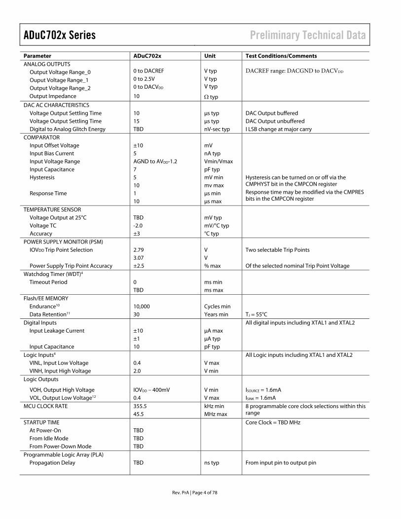
Parameter ADuC702x Unit Test Conditions/Comments ANALOG OUTPUTS
Output Voltage Range_0 Ouput Voltage Range_1 Output Voltage Range_2
0 to DACREF 0 to 2.5V 0 to DACVDD
V typ V typ V typ
DACREF range: DACGND to DACVDD
Output Impedance 10 Ω typ
DAC AC CHARACTERISTICS Voltage Output Settling Time Voltage Output Settling Time Digital to Analog Glitch Energy
10 15 TBD
µs typ µs typ nV-sec typ
DAC Output buffered DAC Output unbuffered I LSB change at major carry
COMPARATOR Input Offset Voltage Input Bias Current Input Voltage Range Input Capacitance Hysteresis Response Time
±10 5 AGND to AVDD-1.2 7 5 10 1 10
mV nA typ Vmin/Vmax pF typ mV min mv max µs min µs max
Hysteresis can be turned on or off via the CMPHYST bit in the CMPCON register Response time may be modified via the CMPRES bits in the CMPCON register
TEMPERATURE SENSOR Voltage Output at 25°C Voltage TC
TBD -2.0
mV typ mV/°C typ
Accuracy ±3 °C typ POWER SUPPLY MONITOR (PSM)
IOVDD Trip Point Selection 2.79 V Two selectable Trip Points 3.07 V Power Supply Trip Point Accuracy ±2.5 % max Of the selected nominal Trip Point Voltage
Watchdog Timer (WDT)4
Timeout Period 0 TBD
ms min ms max
Flash/EE MEMORY Endurance10 10,000 Cycles min Data Retention11 30 Years min TJ = 55°C
Digital Inputs Input Leakage Current Input Capacitance
±10 ±1 10
µA max µA typ pF typ
All digital inputs including XTAL1 and XTAL2
Logic Inputs4 VINL, Input Low Voltage VINH, Input High Voltage
0.4 2.0
V max V min
All Logic inputs including XTAL1 and XTAL2
Logic Outputs
VOH, Output High Voltage IOVDD – 400mV V min ISOURCE = 1.6mA VOL, Output Low Voltage12 0.4 V max ISINK = 1.6mA
MCU CLOCK RATE 355.5 45.5
kHz min MHz max
8 programmable core clock selections within this range
STARTUP TIME At Power-On From Idle Mode From Power-Down Mode
TBD TBD TBD
Core Clock = TBD MHz
Programmable Logic Array (PLA) Propagation Delay
TBD
ns typ
From input pin to output pin
Preliminary Technical Data ADuC702x Series
Rev. PrA | Page 5 of 78
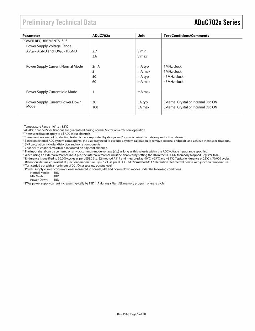
Parameter ADuC702x Unit Test Conditions/Comments POWER REQUIREMENTS 13, 14
Power Supply Voltage Range
AVDD – AGND and IOVDD - IOGND 2.7 V min 3.6 V max
Power Supply Current Normal Mode 3mA 5 50
mA typ mA max mA typ
1MHz clock 1MHz clock 45MHz clock
60 mA max 45MHz clock
Power Supply Current Idle Mode Power Supply Current Power Down Mode
1 30 100
mA max µA typ µA max
External Crystal or Internal Osc ON External Crystal or Internal Osc ON
1 Temperature Range -40° to +85°C 2 All ADC Channel Specifications are guaranteed during normal MicroConverter core operation. 3 These specification apply to all ADC input channels. 4 These numbers are not production tested but are supported by design and/or characterization data on production release. 5 Based on external ADC system components, the user may need to execute a system calibration to remove external endpoint and achieve these specifications.. 6 SNR calculation includes distortion and noise components. 7 Channel-to-channel crosstalk is measured on adjacent channels. 8 The input signal can be centered on any dc common-mode voltage (VCM) as long as this value is within the ADC voltage input range specified. 9 When using an external reference input pin, the internal reference must be disabled by setting the lsb in the REFCON Memeory Mapped Register to 0. 10 Endurance is qualified to 50,000 cycles as per JEDEC Std. 22 method A117 and measured at -40°C, +25°C and +85°C. Typical endurance at 25°C is 70,000 cycles. 11 Retention lifetime equivalent at junction temperature (Tj) = 55°C as per JEDEC Std. 22 method A117. Retention lifetime will derate with junction temperature. 12 Test carried out with a maximum of 20 I/O set to a low output level. 13 Power supply current consumption is measured in normal, idle and power-down modes under the following conditions: Normal Mode: TBD Idle Mode: TBD Power-Down: TBD 14 DVDD power supply current increases typically by TBD mA during a Flash/EE memory program or erase cycle.
ADuC702x Series Preliminary Technical Data
Rev. PrA | Page 6 of 78
TERMINOLOGY ADC Specifications
Integral Nonlinearity
This is the maximum deviation of any code from a straight line passing through the endpoints of the ADC transfer function. The endpoints of the transfer function are zero scale, a point 1/2 LSB below the first code transition and full scale, a point 1/2 LSB above the last code transition.
Differential Nonlinearity
This is the difference between the measured and the ideal 1 LSB change between any two adjacent codes in the ADC.
Offset Error
This is the deviation of the first code transition (0000 . . . 000) to (0000 . . . 001) from the ideal, i.e., +1/2 LSB.
Gain Error
This is the deviation of the last code transition from the ideal AIN voltage (Full Scale – 1.5 LSB) after the offset error has been adjusted out.
Signal to (Noise + Distortion) Ratio
This is the measured ratio of signal to (noise + distortion) at the output of the ADC. The signal is the rms amplitude of the
fundamental. Noise is the rms sum of all nonfundamental signals up to half the sampling frequency (fS/2), excluding dc. The ratio is dependent upon the number of quantization levels in the digitisation process; the more levels, the smaller the quantization noise. The theoretical signal to (noise + distortion) ratio for an ideal N-bit converter with a sine wave input is given by:
Signal to (Noise + Distortion) = (6.02N + 1.76) dB
Thus for a 12-bit converter, this is 74 dB.
Total Harmonic Distortion
Total Harmonic Distortion is the ratio of the rms sum of the harmonics to the fundamental.
DAC SPECIFICATIONS
Relative Accuracy
Relative accuracy or endpoint linearity is a measure of the maximum deviation from a straight line passing through the endpoints of the DAC transfer function. It is measured after adjusting for zero error and full-scale error.
Voltage Output Settling Time
This is the amount of time it takes for the output to settle to within a 1 LSB level for a full-scale input change..
Preliminary Technical Data ADuC702x Series
Rev. PrA | Page 7 of 78
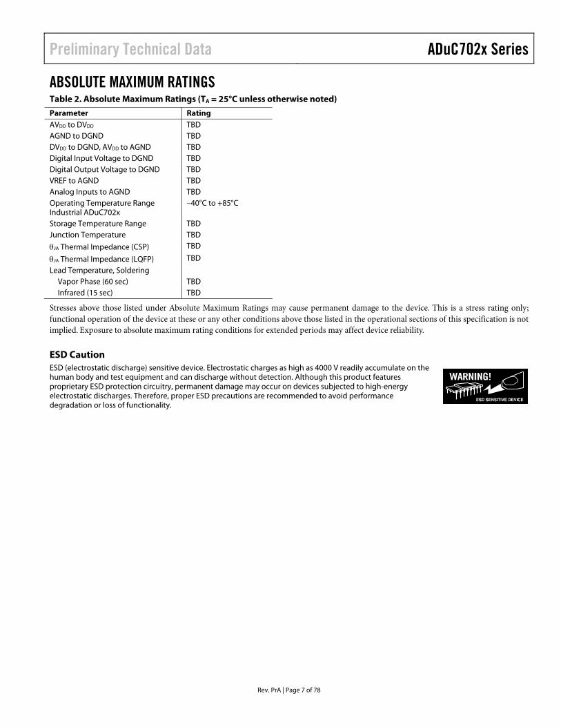
ABSOLUTE MAXIMUM RATINGS Table 2. Absolute Maximum Ratings (TA = 25°C unless otherwise noted)
Parameter Rating AVDD to DVDD TBD AGND to DGND TBD DVDD to DGND, AVDD to AGND TBD Digital Input Voltage to DGND TBD Digital Output Voltage to DGND TBD VREF to AGND TBD Analog Inputs to AGND TBD Operating Temperature Range Industrial ADuC702x
–40°C to +85°C
Storage Temperature Range TBD Junction Temperature TBD
θJA Thermal Impedance (CSP) TBD
θJA Thermal Impedance (LQFP) TBD
Lead Temperature, Soldering Vapor Phase (60 sec) TBD Infrared (15 sec) TBD
Stresses above those listed under Absolute Maximum Ratings may cause permanent damage to the device. This is a stress rating only; functional operation of the device at these or any other conditions above those listed in the operational sections of this specification is not implied. Exposure to absolute maximum rating conditions for extended periods may affect device reliability.
ESD Caution ESD (electrostatic discharge) sensitive device. Electrostatic charges as high as 4000 V readily accumulate on the human body and test equipment and can discharge without detection. Although this product features proprietary ESD protection circuitry, permanent damage may occur on devices subjected to high-energy electrostatic discharges. Therefore, proper ESD precautions are recommended to avoid performance degradation or loss of functionality.
ADuC702x Series Preliminary Technical Data
Rev. PrA | Page 8 of 78
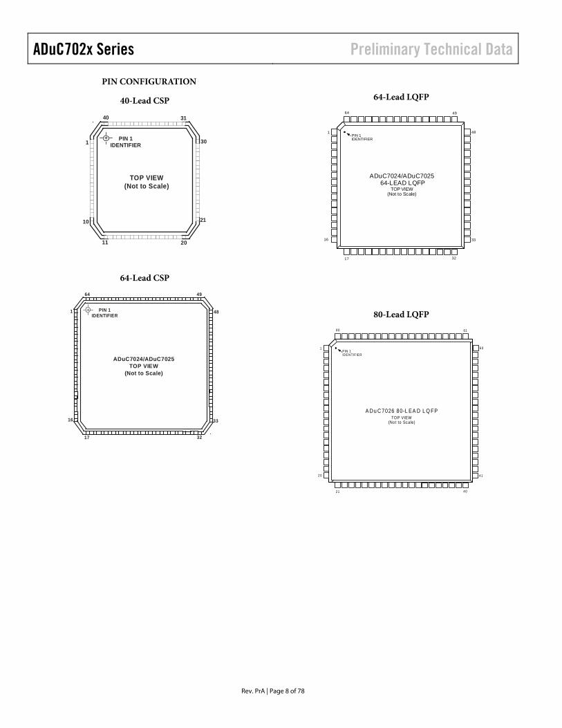
PIN CONFIGURATION
40-Lead CSP
20
31
10
11
PIN 1IDENTIFIER1
40
TOP VIEW(Not to Scale)
30
21
64-Lead CSP
33
32
49
48
16
17
PIN 1IDENTIFIER
1
64
ADuC7024/ADuC7025TOP VIEW
(Not to Scale)
64-Lead LQFP
64 49
17
1
16
48
33
PIN 1IDENTIFIER
TOP VIEW(Not to Scale)
ADuC7024/ADuC702564-LEAD LQFP
32
80-Lead LQFP
80 61
21
1
20
60
41
PIN 1IDENTIFIER
TOP VIEW(No t to Scale)
A D u C 7026 80-L EA D L Q FP
40
Preliminary Technical Data ADuC702x Series
Rev. PrA | Page 9 of 78
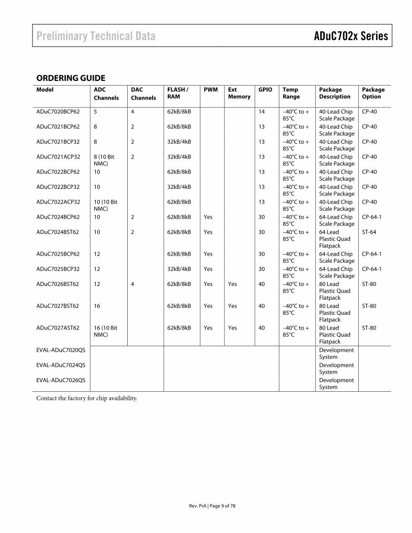
ORDERING GUIDE Model ADC
Channels DAC Channels
FLASH / RAM
PWM Ext Memory
GPIO Temp Range
Package Description
Package Option
ADuC7020BCP62 5 4 62kB/8kB 14 –40°C to + 85°C
40-Lead Chip Scale Package
CP-40
ADuC7021BCP62 8 2 62kB/8kB 13 –40°C to + 85°C
40-Lead Chip Scale Package
CP-40
ADuC7021BCP32 8 2 32kB/4kB 13 –40°C to + 85°C
40-Lead Chip Scale Package
CP-40
ADuC7021ACP32 8 (10 Bit NMC)
2 32kB/4kB 13 –40°C to + 85°C
40-Lead Chip Scale Package
CP-40
ADuC7022BCP62 10 62kB/8kB 13 –40°C to + 85°C
40-Lead Chip Scale Package
CP-40
ADuC7022BCP32 10 32kB/4kB 13 –40°C to + 85°C
40-Lead Chip Scale Package
CP-40
ADuC7022ACP32 10 (10 Bit NMC)
62kB/8kB 13 –40°C to + 85°C
40-Lead Chip Scale Package
CP-40
ADuC7024BCP62 10 2 62kB/8kB Yes 30 –40°C to + 85°C
64-Lead Chip Scale Package
CP-64-1
ADuC7024BST62 10 2 62kB/8kB Yes 30 –40°C to + 85°C
64 Lead Plastic Quad Flatpack
ST-64
ADuC7025BCP62 12 62kB/8kB Yes 30 –40°C to + 85°C
64-Lead Chip Scale Package
CP-64-1
ADuC7025BCP32 12 32kB/4kB Yes 30 –40°C to + 85°C
64-Lead Chip Scale Package
CP-64-1
ADuC7026BST62 12 4 62kB/8kB Yes Yes 40 –40°C to + 85°C
80 Lead Plastic Quad Flatpack
ST-80
ADuC7027BST62 16 62kB/8kB Yes Yes 40 –40°C to + 85°C
80 Lead Plastic Quad Flatpack
ST-80
ADuC7027AST62 16 (10 Bit NMC)
62kB/8kB Yes Yes 40 –40°C to + 85°C
80 Lead Plastic Quad Flatpack
ST-80
EVAL-ADuC7020QS Development System
EVAL-ADuC7024QS Development System
EVAL-ADuC7026QS Development System
Contact the factory for chip availability.
ADuC702x Series Preliminary Technical Data
Rev. PrA | Page 10 of 78
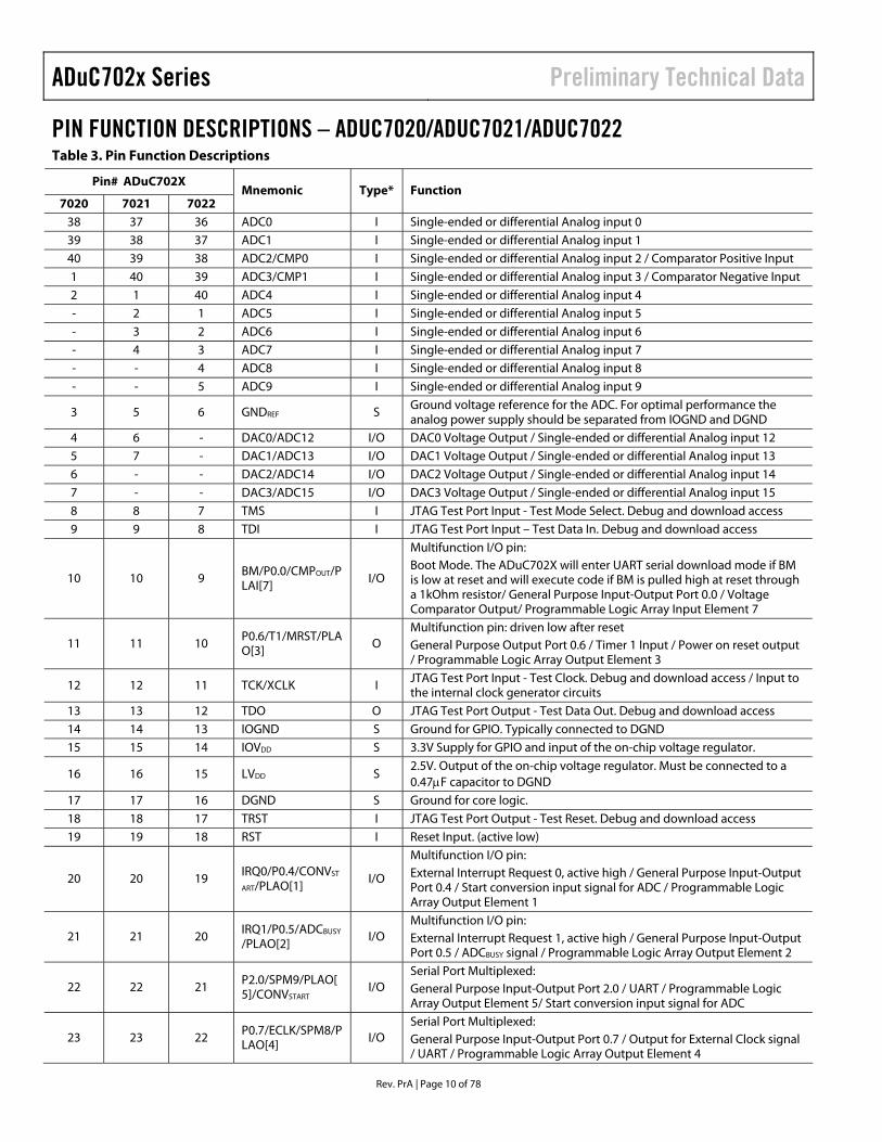
PIN FUNCTION DESCRIPTIONS – ADUC7020/ADUC7021/ADUC7022 Table 3. Pin Function Descriptions
Pin# ADuC702X
7020 7021 7022 Mnemonic Type* Function
38 37 36 ADC0 I Single-ended or differential Analog input 0 39 38 37 ADC1 I Single-ended or differential Analog input 1 40 39 38 ADC2/CMP0 I Single-ended or differential Analog input 2 / Comparator Positive Input 1 40 39 ADC3/CMP1 I Single-ended or differential Analog input 3 / Comparator Negative Input 2 1 40 ADC4 I Single-ended or differential Analog input 4 - 2 1 ADC5 I Single-ended or differential Analog input 5 - 3 2 ADC6 I Single-ended or differential Analog input 6 - 4 3 ADC7 I Single-ended or differential Analog input 7 - - 4 ADC8 I Single-ended or differential Analog input 8 - - 5 ADC9 I Single-ended or differential Analog input 9
3 5 6 GNDREF S Ground voltage reference for the ADC. For optimal performance the analog power supply should be separated from IOGND and DGND
4 6 - DAC0/ADC12 I/O DAC0 Voltage Output / Single-ended or differential Analog input 12 5 7 - DAC1/ADC13 I/O DAC1 Voltage Output / Single-ended or differential Analog input 13 6 - - DAC2/ADC14 I/O DAC2 Voltage Output / Single-ended or differential Analog input 14 7 - - DAC3/ADC15 I/O DAC3 Voltage Output / Single-ended or differential Analog input 15 8 8 7 TMS I JTAG Test Port Input - Test Mode Select. Debug and download access 9 9 8 TDI I JTAG Test Port Input – Test Data In. Debug and download access
10 10 9 BM/P0.0/CMPOUT/PLAI[7]
I/O
Multifunction I/O pin: Boot Mode. The ADuC702X will enter UART serial download mode if BM is low at reset and will execute code if BM is pulled high at reset through a 1kOhm resistor/ General Purpose Input-Output Port 0.0 / Voltage Comparator Output/ Programmable Logic Array Input Element 7
11 11 10 P0.6/T1/MRST/PLAO[3]
O Multifunction pin: driven low after reset General Purpose Output Port 0.6 / Timer 1 Input / Power on reset output / Programmable Logic Array Output Element 3
12 12 11 TCK/XCLK I JTAG Test Port Input - Test Clock. Debug and download access / Input to the internal clock generator circuits
13 13 12 TDO O JTAG Test Port Output - Test Data Out. Debug and download access 14 14 13 IOGND S Ground for GPIO. Typically connected to DGND 15 15 14 IOVDD S 3.3V Supply for GPIO and input of the on-chip voltage regulator.
16 16 15 LVDD S 2.5V. Output of the on-chip voltage regulator. Must be connected to a 0.47µF capacitor to DGND
17 17 16 DGND S Ground for core logic. 18 18 17 TRST I JTAG Test Port Output - Test Reset. Debug and download access 19 19 18 RST I Reset Input. (active low)
20 20 19 IRQ0/P0.4/CONVST
ART/PLAO[1] I/O
Multifunction I/O pin: External Interrupt Request 0, active high / General Purpose Input-Output Port 0.4 / Start conversion input signal for ADC / Programmable Logic Array Output Element 1
21 21 20 IRQ1/P0.5/ADCBUSY
/PLAO[2] I/O
Multifunction I/O pin: External Interrupt Request 1, active high / General Purpose Input-Output Port 0.5 / ADCBUSY signal / Programmable Logic Array Output Element 2
22 22 21 P2.0/SPM9/PLAO[5]/CONVSTART
I/O Serial Port Multiplexed: General Purpose Input-Output Port 2.0 / UART / Programmable Logic Array Output Element 5/ Start conversion input signal for ADC
23 23 22 P0.7/ECLK/SPM8/PLAO[4]
I/O Serial Port Multiplexed: General Purpose Input-Output Port 0.7 / Output for External Clock signal / UART / Programmable Logic Array Output Element 4
Preliminary Technical Data ADuC702x Series
Rev. PrA | Page 11 of 78
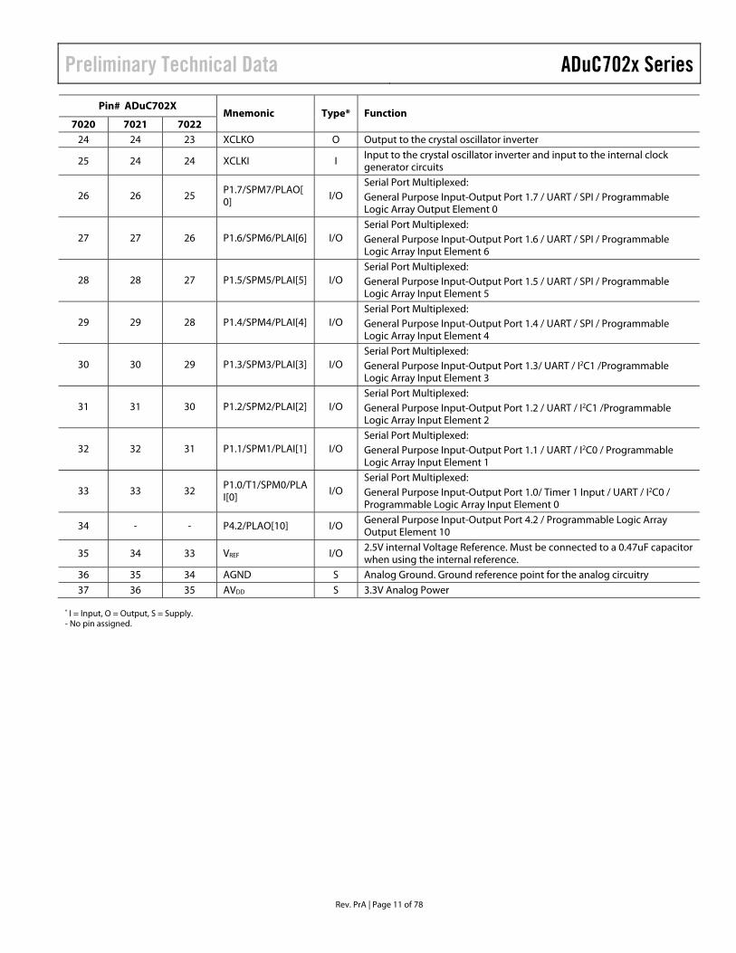
Pin# ADuC702X
7020 7021 7022 Mnemonic Type* Function
24 24 23 XCLKO O Output to the crystal oscillator inverter
25 24 24 XCLKI I Input to the crystal oscillator inverter and input to the internal clock generator circuits
26 26 25 P1.7/SPM7/PLAO[0]
I/O Serial Port Multiplexed: General Purpose Input-Output Port 1.7 / UART / SPI / Programmable Logic Array Output Element 0
27 27 26 P1.6/SPM6/PLAI[6] I/O Serial Port Multiplexed: General Purpose Input-Output Port 1.6 / UART / SPI / Programmable Logic Array Input Element 6
28 28 27 P1.5/SPM5/PLAI[5] I/O Serial Port Multiplexed: General Purpose Input-Output Port 1.5 / UART / SPI / Programmable Logic Array Input Element 5
29 29 28 P1.4/SPM4/PLAI[4] I/O Serial Port Multiplexed: General Purpose Input-Output Port 1.4 / UART / SPI / Programmable Logic Array Input Element 4
30 30 29 P1.3/SPM3/PLAI[3] I/O Serial Port Multiplexed: General Purpose Input-Output Port 1.3/ UART / I2C1 /Programmable Logic Array Input Element 3
31 31 30 P1.2/SPM2/PLAI[2] I/O Serial Port Multiplexed: General Purpose Input-Output Port 1.2 / UART / I2C1 /Programmable Logic Array Input Element 2
32 32 31 P1.1/SPM1/PLAI[1] I/O Serial Port Multiplexed: General Purpose Input-Output Port 1.1 / UART / I2C0 / Programmable Logic Array Input Element 1
33 33 32 P1.0/T1/SPM0/PLAI[0]
I/O Serial Port Multiplexed: General Purpose Input-Output Port 1.0/ Timer 1 Input / UART / I2C0 / Programmable Logic Array Input Element 0
34 - - P4.2/PLAO[10] I/O General Purpose Input-Output Port 4.2 / Programmable Logic Array Output Element 10
35 34 33 VREF I/O 2.5V internal Voltage Reference. Must be connected to a 0.47uF capacitor when using the internal reference.
36 35 34 AGND S Analog Ground. Ground reference point for the analog circuitry 37 36 35 AVDD S 3.3V Analog Power
* I = Input, O = Output, S = Supply. - No pin assigned.
ADuC702x Series Preliminary Technical Data
Rev. PrA | Page 12 of 78
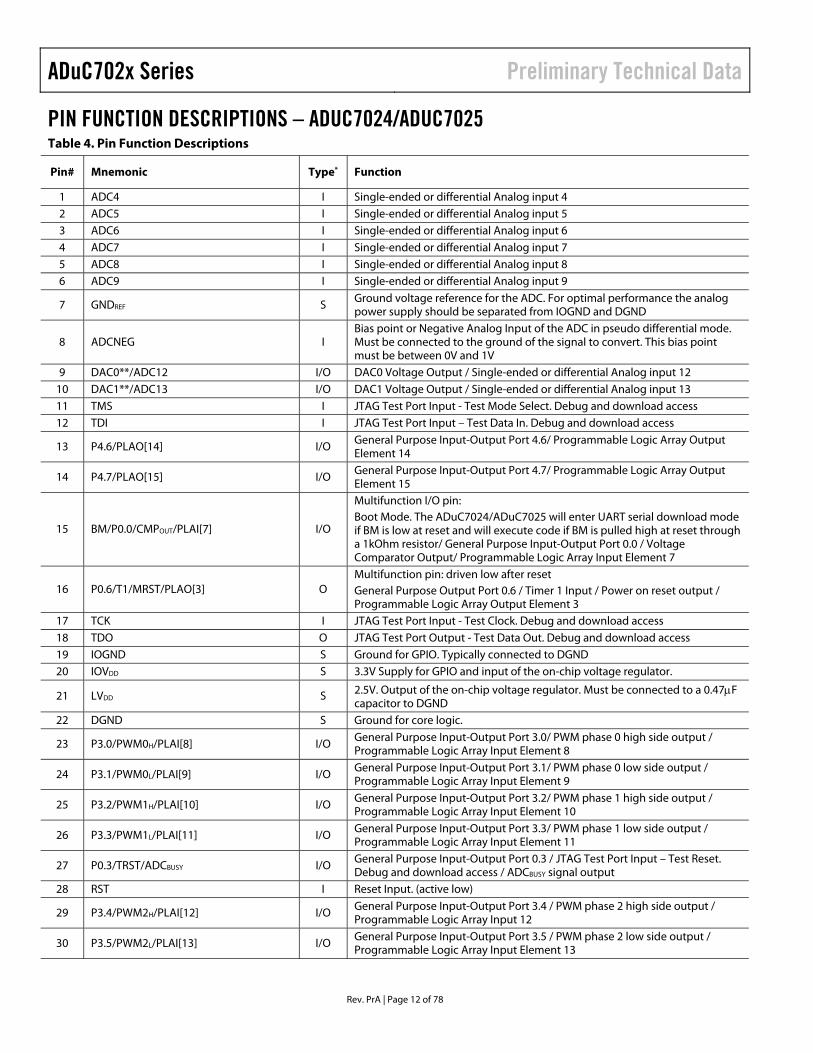
PIN FUNCTION DESCRIPTIONS – ADUC7024/ADUC7025 Table 4. Pin Function Descriptions
Pin# Mnemonic Type* Function
1 ADC4 I Single-ended or differential Analog input 4 2 ADC5 I Single-ended or differential Analog input 5 3 ADC6 I Single-ended or differential Analog input 6 4 ADC7 I Single-ended or differential Analog input 7 5 ADC8 I Single-ended or differential Analog input 8 6 ADC9 I Single-ended or differential Analog input 9
7 GNDREF S Ground voltage reference for the ADC. For optimal performance the analog power supply should be separated from IOGND and DGND
8 ADCNEG I Bias point or Negative Analog Input of the ADC in pseudo differential mode. Must be connected to the ground of the signal to convert. This bias point must be between 0V and 1V
9 DAC0**/ADC12 I/O DAC0 Voltage Output / Single-ended or differential Analog input 12 10 DAC1**/ADC13 I/O DAC1 Voltage Output / Single-ended or differential Analog input 13 11 TMS I JTAG Test Port Input - Test Mode Select. Debug and download access 12 TDI I JTAG Test Port Input – Test Data In. Debug and download access
13 P4.6/PLAO[14] I/O General Purpose Input-Output Port 4.6/ Programmable Logic Array Output Element 14
14 P4.7/PLAO[15] I/O General Purpose Input-Output Port 4.7/ Programmable Logic Array Output Element 15
15 BM/P0.0/CMPOUT/PLAI[7] I/O
Multifunction I/O pin: Boot Mode. The ADuC7024/ADuC7025 will enter UART serial download mode if BM is low at reset and will execute code if BM is pulled high at reset through a 1kOhm resistor/ General Purpose Input-Output Port 0.0 / Voltage Comparator Output/ Programmable Logic Array Input Element 7
16 P0.6/T1/MRST/PLAO[3] O Multifunction pin: driven low after reset General Purpose Output Port 0.6 / Timer 1 Input / Power on reset output / Programmable Logic Array Output Element 3
17 TCK I JTAG Test Port Input - Test Clock. Debug and download access 18 TDO O JTAG Test Port Output - Test Data Out. Debug and download access 19 IOGND S Ground for GPIO. Typically connected to DGND 20 IOVDD S 3.3V Supply for GPIO and input of the on-chip voltage regulator.
21 LVDD S 2.5V. Output of the on-chip voltage regulator. Must be connected to a 0.47µF capacitor to DGND
22 DGND S Ground for core logic.
23 P3.0/PWM0H/PLAI[8] I/O General Purpose Input-Output Port 3.0/ PWM phase 0 high side output / Programmable Logic Array Input Element 8
24 P3.1/PWM0L/PLAI[9] I/O General Purpose Input-Output Port 3.1/ PWM phase 0 low side output / Programmable Logic Array Input Element 9
25 P3.2/PWM1H/PLAI[10] I/O General Purpose Input-Output Port 3.2/ PWM phase 1 high side output / Programmable Logic Array Input Element 10
26 P3.3/PWM1L/PLAI[11] I/O General Purpose Input-Output Port 3.3/ PWM phase 1 low side output / Programmable Logic Array Input Element 11
27 P0.3/TRST/ADCBUSY I/O General Purpose Input-Output Port 0.3 / JTAG Test Port Input – Test Reset. Debug and download access / ADCBUSY signal output
28 RST I Reset Input. (active low)
29 P3.4/PWM2H/PLAI[12] I/O General Purpose Input-Output Port 3.4 / PWM phase 2 high side output / Programmable Logic Array Input 12
30 P3.5/PWM2L/PLAI[13] I/O General Purpose Input-Output Port 3.5 / PWM phase 2 low side output / Programmable Logic Array Input Element 13
Preliminary Technical Data ADuC702x Series
Rev. PrA | Page 13 of 78
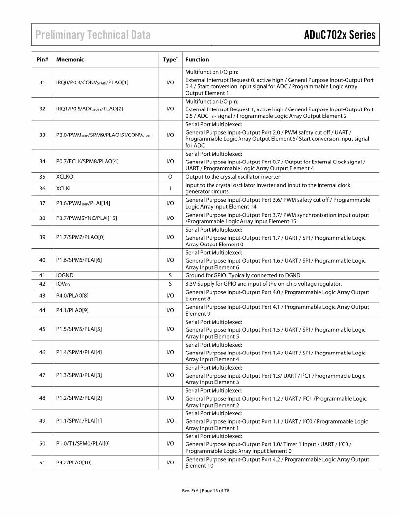
Pin# Mnemonic Type* Function
31 IRQ0/P0.4/CONVSTART/PLAO[1] I/O
Multifunction I/O pin: External Interrupt Request 0, active high / General Purpose Input-Output Port 0.4 / Start conversion input signal for ADC / Programmable Logic Array Output Element 1
32 IRQ1/P0.5/ADCBUSY/PLAO[2] I/O Multifunction I/O pin: External Interrupt Request 1, active high / General Purpose Input-Output Port 0.5 / ADCBUSY signal / Programmable Logic Array Output Element 2
33 P2.0/PWMTRIP/SPM9/PLAO[5]/CONVSTART I/O
Serial Port Multiplexed: General Purpose Input-Output Port 2.0 / PWM safety cut off / UART / Programmable Logic Array Output Element 5/ Start conversion input signal for ADC
34 P0.7/ECLK/SPM8/PLAO[4] I/O Serial Port Multiplexed: General Purpose Input-Output Port 0.7 / Output for External Clock signal / UART / Programmable Logic Array Output Element 4
35 XCLKO O Output to the crystal oscillator inverter
36 XCLKI I Input to the crystal oscillator inverter and input to the internal clock generator circuits
37 P3.6/PWMTRIP/PLAI[14] I/O General Purpose Input-Output Port 3.6/ PWM safety cut off / Programmable Logic Array Input Element 14
38 P3.7/PWMSYNC/PLAI[15] I/O General Purpose Input-Output Port 3.7/ PWM synchronisation input output /Programmable Logic Array Input Element 15
39 P1.7/SPM7/PLAO[0] I/O Serial Port Multiplexed: General Purpose Input-Output Port 1.7 / UART / SPI / Programmable Logic Array Output Element 0
40 P1.6/SPM6/PLAI[6] I/O Serial Port Multiplexed: General Purpose Input-Output Port 1.6 / UART / SPI / Programmable Logic Array Input Element 6
41 IOGND S Ground for GPIO. Typically connected to DGND 42 IOVDD S 3.3V Supply for GPIO and input of the on-chip voltage regulator.
43 P4.0/PLAO[8] I/O General Purpose Input-Output Port 4.0 / Programmable Logic Array Output Element 8
44 P4.1/PLAO[9] I/O General Purpose Input-Output Port 4.1 / Programmable Logic Array Output Element 9
45 P1.5/SPM5/PLAI[5] I/O Serial Port Multiplexed: General Purpose Input-Output Port 1.5 / UART / SPI / Programmable Logic Array Input Element 5
46 P1.4/SPM4/PLAI[4] I/O Serial Port Multiplexed: General Purpose Input-Output Port 1.4 / UART / SPI / Programmable Logic Array Input Element 4
47 P1.3/SPM3/PLAI[3] I/O Serial Port Multiplexed: General Purpose Input-Output Port 1.3/ UART / I2C1 /Programmable Logic Array Input Element 3
48 P1.2/SPM2/PLAI[2] I/O Serial Port Multiplexed: General Purpose Input-Output Port 1.2 / UART / I2C1 /Programmable Logic Array Input Element 2
49 P1.1/SPM1/PLAI[1] I/O Serial Port Multiplexed: General Purpose Input-Output Port 1.1 / UART / I2C0 / Programmable Logic Array Input Element 1
50 P1.0/T1/SPM0/PLAI[0] I/O Serial Port Multiplexed: General Purpose Input-Output Port 1.0/ Timer 1 Input / UART / I2C0 / Programmable Logic Array Input Element 0
51 P4.2/PLAO[10] I/O General Purpose Input-Output Port 4.2 / Programmable Logic Array Output Element 10
ADuC702x Series Preliminary Technical Data
Rev. PrA | Page 14 of 78
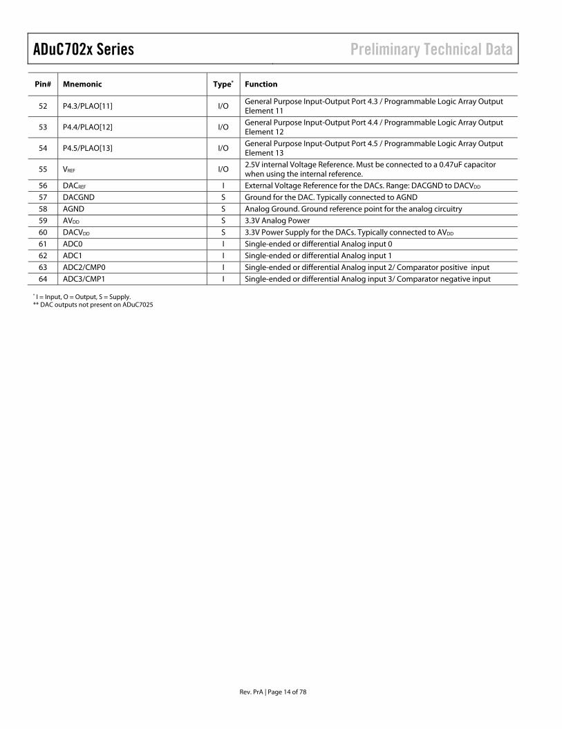
Pin# Mnemonic Type* Function
52 P4.3/PLAO[11] I/O General Purpose Input-Output Port 4.3 / Programmable Logic Array Output Element 11
53 P4.4/PLAO[12] I/O General Purpose Input-Output Port 4.4 / Programmable Logic Array Output Element 12
54 P4.5/PLAO[13] I/O General Purpose Input-Output Port 4.5 / Programmable Logic Array Output Element 13
55 VREF I/O 2.5V internal Voltage Reference. Must be connected to a 0.47uF capacitor when using the internal reference.
56 DACREF I External Voltage Reference for the DACs. Range: DACGND to DACVDD 57 DACGND S Ground for the DAC. Typically connected to AGND 58 AGND S Analog Ground. Ground reference point for the analog circuitry 59 AVDD S 3.3V Analog Power 60 DACVDD S 3.3V Power Supply for the DACs. Typically connected to AVDD 61 ADC0 I Single-ended or differential Analog input 0 62 ADC1 I Single-ended or differential Analog input 1 63 ADC2/CMP0 I Single-ended or differential Analog input 2/ Comparator positive input 64 ADC3/CMP1 I Single-ended or differential Analog input 3/ Comparator negative input
* I = Input, O = Output, S = Supply. ** DAC outputs not present on ADuC7025
Preliminary Technical Data ADuC702x Series
Rev. PrA | Page 15 of 78
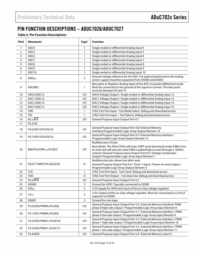
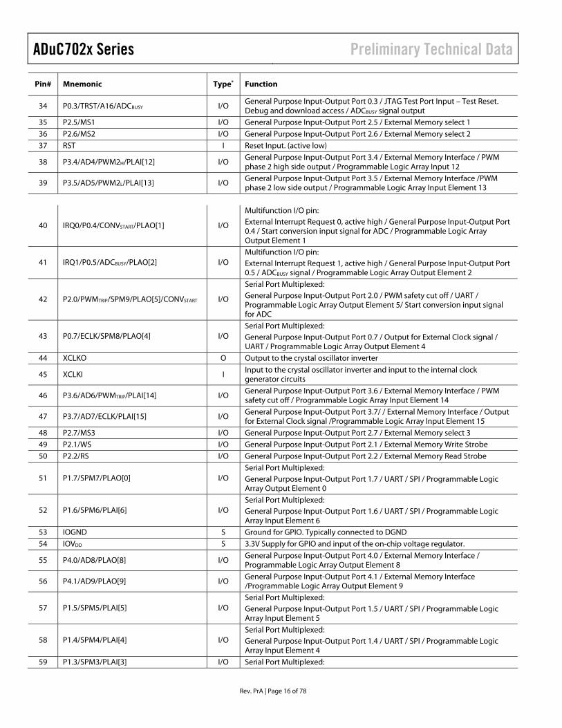
PIN FUNCTION DESCRIPTIONS – ADUC7026/ADUC7027 Table 5. Pin Function Descriptions
Pin# Mnemonic Type* Function
1 ADC4 I Single-ended or differential Analog input 4 2 ADC5 I Single-ended or differential Analog input 5 3 ADC6 I Single-ended or differential Analog input 6 4 ADC7 I Single-ended or differential Analog input 7 5 ADC8 I Single-ended or differential Analog input 8 6 ADC9 I Single-ended or differential Analog input 9 7 ADC10 I Single-ended or differential Analog input 10
8 GNDREF S Ground voltage reference for the ADC. For optimal performance the analog power supply should be separated from IOGND and DGND
9 ADCNEG I Bias point or Negative Analog Input of the ADC in pseudo differential mode. Must be connected to the ground of the signal to convert. This bias point must be between 0V and 1V
10 DAC0/ADC12 I/O DAC0 Voltage Output / Single-ended or differential Analog input 12 11 DAC1/ADC13 I/O DAC1 Voltage Output / Single-ended or differential Analog input 13 12 DAC1/ADC14 I/O DAC2 Voltage Output / Single-ended or differential Analog input 14 13 DAC1/ADC15 I/O DAC3 Voltage Output / Single-ended or differential Analog input 15 14 TMS I JTAG Test Port Input - Test Mode Select. Debug and download access 15 TDI I JTAG Test Port Input – Test Data In. Debug and download access
16 P0.1/BLE I/O General Purpose Input-Output Port 0.1
17 P2.3/AE
18 P4.6/AD14/PLAO[14] I/O General Purpose Input-Output Port 4.6/ External Memory Interface/Programmable Logic Array Output Element 14
19 P4.7/AD15/PLAO[15] I/O General Purpose Input-Output Port 4.7/ External Memory Interface / Programmable Logic Array Output Element 15
20 BM/P0.0/CMPOUT/PLAI[7] I/O
Multifunction I/O pin: Boot Mode. The ADuC7026 will enter UART serial download mode if BM is low at reset and will execute code if BM is pulled high at reset through a 1kOhm resistor/ General Purpose Input-Output Port 0.0 / Voltage Comparator Output/ Programmable Logic Array Input Element 7
21 P0.6/T1/MRST/PLAO[3]/AE O Multifunction pin: driven low after reset General Purpose Output Port 0.6 / Timer 1 Input / Power on reset output / Programmable Logic Array Output Element 3
22 TCK I JTAG Test Port Input - Test Clock. Debug and download access 23 TDO O JTAG Test Port Output - Test Data Out. Debug and download access
24 P0.2/BHE I/O General Purpose Input-Output Port 0.2
25 IOGND S Ground for GPIO. Typically connected to DGND 26 IOVDD S 3.3V Supply for GPIO and input of the on-chip voltage regulator.
27 LVDD S 2.5V. Output of the on-chip voltage regulator. Must be connected to a 0.47µF capacitor to DGND
28 DGND S Ground for core logic.
29 P3.0/AD0/PWM0H/PLAI[8] I/O General Purpose Input-Output Port 3.0 / External Memory Interface/ PWM phase 0 high side output / Programmable Logic Array Input Element 8
30 P3.1/AD1/PWM0L/PLAI[9] I/O General Purpose Input-Output Port 3.1 / External Memory Interface / PWM phase 0 low side output / Programmable Logic Array Input Element 9
31 P3.2/AD2/PWM1H/PLAI[10] I/O General Purpose Input-Output Port 3.2 / External Memory Interface / PWM phase 1 high side output / Programmable Logic Array Input Element 10
32 P3.3/AD3/PWM1L/PLAI[11] I/O General Purpose Input-Output Port 3.3 / External Memory Interface / PWM phase 1 low side output / Programmable Logic Array Input Element 11
33 P2.4/MS0 I/O General Purpose Input-Output Port 2.4 / External Memory select 0
ADuC702x Series Preliminary Technical Data
Rev. PrA | Page 16 of 78
Pin# Mnemonic Type* Function
34 P0.3/TRST/A16/ADCBUSY I/O General Purpose Input-Output Port 0.3 / JTAG Test Port Input – Test Reset. Debug and download access / ADCBUSY signal output
35 P2.5/MS1 I/O General Purpose Input-Output Port 2.5 / External Memory select 1 36 P2.6/MS2 I/O General Purpose Input-Output Port 2.6 / External Memory select 2 37 RST I Reset Input. (active low)
38 P3.4/AD4/PWM2H/PLAI[12] I/O General Purpose Input-Output Port 3.4 / External Memory Interface / PWM phase 2 high side output / Programmable Logic Array Input 12
39 P3.5/AD5/PWM2L/PLAI[13] I/O General Purpose Input-Output Port 3.5 / External Memory Interface /PWM phase 2 low side output / Programmable Logic Array Input Element 13
40 IRQ0/P0.4/CONVSTART/PLAO[1] I/O
Multifunction I/O pin: External Interrupt Request 0, active high / General Purpose Input-Output Port 0.4 / Start conversion input signal for ADC / Programmable Logic Array Output Element 1
41 IRQ1/P0.5/ADCBUSY/PLAO[2] I/O Multifunction I/O pin: External Interrupt Request 1, active high / General Purpose Input-Output Port 0.5 / ADCBUSY signal / Programmable Logic Array Output Element 2
42 P2.0/PWMTRIP/SPM9/PLAO[5]/CONVSTART I/O
Serial Port Multiplexed: General Purpose Input-Output Port 2.0 / PWM safety cut off / UART / Programmable Logic Array Output Element 5/ Start conversion input signal for ADC
43 P0.7/ECLK/SPM8/PLAO[4] I/O Serial Port Multiplexed: General Purpose Input-Output Port 0.7 / Output for External Clock signal / UART / Programmable Logic Array Output Element 4
44 XCLKO O Output to the crystal oscillator inverter
45 XCLKI I Input to the crystal oscillator inverter and input to the internal clock generator circuits
46 P3.6/AD6/PWMTRIP/PLAI[14] I/O General Purpose Input-Output Port 3.6 / External Memory Interface / PWM safety cut off / Programmable Logic Array Input Element 14
47 P3.7/AD7/ECLK/PLAI[15] I/O General Purpose Input-Output Port 3.7/ / External Memory Interface / Output for External Clock signal /Programmable Logic Array Input Element 15
48 P2.7/MS3 I/O General Purpose Input-Output Port 2.7 / External Memory select 3 49 P2.1/WS I/O General Purpose Input-Output Port 2.1 / External Memory Write Strobe 50 P2.2/RS I/O General Purpose Input-Output Port 2.2 / External Memory Read Strobe
51 P1.7/SPM7/PLAO[0] I/O Serial Port Multiplexed: General Purpose Input-Output Port 1.7 / UART / SPI / Programmable Logic Array Output Element 0
52 P1.6/SPM6/PLAI[6] I/O Serial Port Multiplexed: General Purpose Input-Output Port 1.6 / UART / SPI / Programmable Logic Array Input Element 6
53 IOGND S Ground for GPIO. Typically connected to DGND 54 IOVDD S 3.3V Supply for GPIO and input of the on-chip voltage regulator.
55 P4.0/AD8/PLAO[8] I/O General Purpose Input-Output Port 4.0 / External Memory Interface / Programmable Logic Array Output Element 8
56 P4.1/AD9/PLAO[9] I/O General Purpose Input-Output Port 4.1 / External Memory Interface /Programmable Logic Array Output Element 9
57 P1.5/SPM5/PLAI[5] I/O Serial Port Multiplexed: General Purpose Input-Output Port 1.5 / UART / SPI / Programmable Logic Array Input Element 5
58 P1.4/SPM4/PLAI[4] I/O Serial Port Multiplexed: General Purpose Input-Output Port 1.4 / UART / SPI / Programmable Logic Array Input Element 4
59 P1.3/SPM3/PLAI[3] I/O Serial Port Multiplexed:
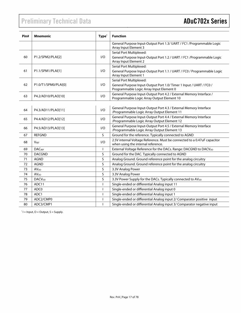
Preliminary Technical Data ADuC702x Series
Rev. PrA | Page 17 of 78
Pin# Mnemonic Type* Function
General Purpose Input-Output Port 1.3/ UART / I2C1 /Programmable Logic Array Input Element 3
60 P1.2/SPM2/PLAI[2] I/O Serial Port Multiplexed: General Purpose Input-Output Port 1.2 / UART / I2C1 /Programmable Logic Array Input Element 2
61 P1.1/SPM1/PLAI[1] I/O Serial Port Multiplexed: General Purpose Input-Output Port 1.1 / UART / I2C0 / Programmable Logic Array Input Element 1
62 P1.0/T1/SPM0/PLAI[0] I/O Serial Port Multiplexed: General Purpose Input-Output Port 1.0/ Timer 1 Input / UART / I2C0 / Programmable Logic Array Input Element 0
63 P4.2/AD10/PLAO[10] I/O General Purpose Input-Output Port 4.2 / External Memory Interface / Programmable Logic Array Output Element 10
64 P4.3/AD11/PLAO[11] I/O General Purpose Input-Output Port 4.3 / External Memory Interface /Programmable Logic Array Output Element 11
65 P4.4/AD12/PLAO[12] I/O General Purpose Input-Output Port 4.4 / External Memory Interface /Programmable Logic Array Output Element 12
66 P4.5/AD13/PLAO[13] I/O General Purpose Input-Output Port 4.5 / External Memory Interface /Programmable Logic Array Output Element 13
67 REFGND S Ground for the reference. Typically connected to AGND
68 VREF I/O 2.5V internal Voltage Reference. Must be connected to a 0.47uF capacitor when using the internal reference.
69 DACREF I External Voltage Reference for the DACs. Range: DACGND to DACVDD 70 DACGND S Ground for the DAC. Typically connected to AGND 71 AGND S Analog Ground. Ground reference point for the analog circuitry 72 AGND S Analog Ground. Ground reference point for the analog circuitry 73 AVDD S 3.3V Analog Power 74 AVDD S 3.3V Analog Power 75 DACVDD S 3.3V Power Supply for the DACs. Typically connected to AVDD 76 ADC11 I Single-ended or differential Analog input 11 77 ADC0 I Single-ended or differential Analog input 0 78 ADC1 I Single-ended or differential Analog input 1 79 ADC2/CMP0 I Single-ended or differential Analog input 2/ Comparator positive input 80 ADC3/CMP1 I Single-ended or differential Analog input 3/ Comparator negative input
* I = Input, O = Output, S = Supply.
ADuC702x Series Preliminary Technical Data
Rev. PrA | Page 18 of 78
P1.7
/SPM
7/PL
AI
P1.6
/SPM
6/PL
AI
P1.5
/SPM
5/PL
AI
P1.4
/SPM
4/PL
AI
P1.3
/SPM
3/PL
AI
P1.2
/SPM
2/PL
AI
P1.1
/SPM
1/PL
AI
P1. 0
/SPM
0/PL
AI
P0.7
/EC
LK/S
PM8/
PLA
O
P2.0
/PW
MTR
IP/S
PM9/
PLA
O/C
OM
V STA
RT
TCK
/XC
LKP0
.3/T
RST
/A16
/AD
CB
US
Y
TDO
TDI
TMS
UARTSERIAL PORT
SPI/I2C SERIALINTERFACE
SERIAL PORT MULTIPLEXER
IRQ1/P0.5/ADCBUSY/PLAO
IRQ0/P0.4/CONVSTART/PLAO
OSC
PROG. CLOCKDIVIDER
XCLKOXCLKIPLL
PROG. LOGICARRAY
INTERRUPTCONTROLLER
P4.6/PLAO/AD14
P4.7/PLAO/AD15
P4.0
/PLA
O/A
D8
P4.2
/PLA
O/A
D10
P4.3
/PLA
O/A
D11
P4.1
/PLA
O/A
D9
P4.5
/PLA
O/A
D13
P4.4
/PLA
O/A
D12
POR
P0.6
/MR
ST/P
LAO
/AE
JTAG
EMUL
ATO
R
8192 BYTES USER RAM(2k X 32 bits)
POWER SUPPLYMONITOR
ARM7TDMI
MCUCORE
62 KBYTES FLASH/EE(31k X 16 bits)
DOWNLOADER
VREFMUX
DACVREF
BAND GAPREFERENCE
WAKEUP/RTC TIMER
RES
ET
GN
DR
EF
AG
ND
IOG
ND
IOV D
D
DG
ND
LVD
D
IOG
ND
IOV D
D
ADC0
TEMPSENSOR
ADC1
MUX
12-BIT SARADC 1MSPS
ADCCONTROL
DA
CV D
D
DA
CR
EF
DA
CG
ND
ADuC7026*
DAC2*/ADC14BUF12-BIT
VOLTAGEOUTPUT DAC
DAC3*/ADC15BUF12-BIT
VOLTAGEOUTPUT DAC
DACCONTROL
P3.6/PWMTRIP/PLAI/AD6P3.5/PWM2H/PLAI/AD5P3.4/PWM2H/PLAI/AD4P3.3/PWM1H/PLAI/AD3P3.2/PWM1H/PLAI/AD2P3.1/PWM0L/PLAI/AD1P3.0/PWM0H/PLAI/AD0
Three-phasePWM
ADC2/CMP0
ADC8
ADC4ADC3/CMP1
ADC9
ADCNEG
MUXDACCMPOUT/IRQ
BM/P0.0/CMPOUT/PLAO
ADC7ADC6ADC5
P3.7/ECLK/PLAI/AD7
* See selection table forfeature availability ondifferent models.
ADC10ADC11
DAC1*/ADC13BUF12-BIT
VOLTAGEOUTPUT DAC
DAC0*/ADC12BUF12-BIT
VOLTAGEOUTPUT DAC
P0.2
/BH
EP0
.1/B
LE
P2.2
/RS
P2.3
/AE
P2.4
/MS0
P2.5
/MS1
P2.6
/MS2
P2.1
/WS
P2.7
/MS3
P0.0
REF
GN
D
AV D
D
AV D
D
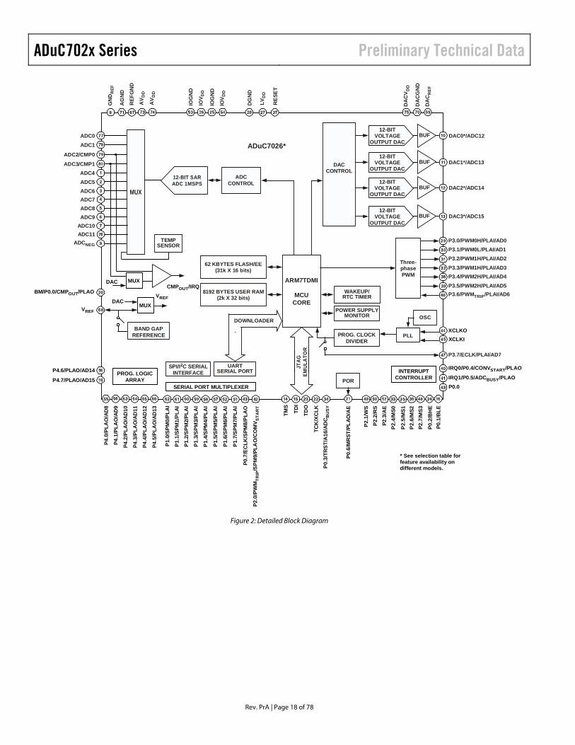
Figure 2: Detailed Block Diagram
Preliminary Technical Data ADuC702x Series
Rev. PrA | Page 19 of 78
GENERAL DESCRIPTION The ADuC702x is fully integrated, 1MSPS, 12-bit data acquisition system incorporating a high performance multi-channel ADC, a 16/32-bit MCU and Flash/EE Memory on a single chip.
The ADC consists of up to 12 single-ended inputs. An additional 4 inputs are available but are multiplexed with the 4 DAC output pins. The 4 DAC outputs are only available on certain models of the ADuC702x, though in many cases where the DAC is not present this pin can still be used as an additional ADC input, giving a maximum of 16 ADC input channels. The ADC can operate in single-ended or differential input modes. The ADC input voltage is 0 to VREF. Low drift bandgap reference, temperature sensor and voltage comparator complete the ADC peripheral set.
The ADuC702x also integrates 4 buffered voltage output DACs on-chip. The DAC output range is programmable to one of three voltage ranges.
The device operates from an on-chip oscillator and PLL generating an internal high-frequency clock of 45 MHz. This clock is routed through a programmable clock divider from which the MCU core clock operating frequency is generated. The microcontroller core is an ARM7TDMI, 16/32-bit RISC machine, offering up to 45 MIPS peak performance. 62k Bytes of non-volatile Flash/EE are provided on-chip as well as 8k Bytes of SRAM. Both the Flash/EE and SRAM memory arrays are mapped into a single linear array.
On-chip factory firmware supports in-circuit serial download via the UART and JTAG serial interface ports while non-intrusive emulation is also supported via the JTAG interface. These features are incorporated into a low-cost QuickStart Development System supporting this MicroConverter family.
The parts operate from 2.7V to 3.6V and are specified over an industrial temperature range of -40°C to 85°C. When operating at 45MHz the power dissipation is 300mW. The ADuC702x is available in a variety of memory models and packages. These are detailed on page 9.
OVERVIEW OF THE ARM7TDMI CORE
The ARM7 core is a 32-bit Reduced Instruction Set Computer (RISC). It uses a single 32-bit bus for instruction and data. The length of the data can be 8, 16 or 32 bits and the length of the instruction word is 32 bits.
The ARM7TDMI is an ARM7 core with 4 additional features: - T support for the Thumb (16 bit) instruction set. - D support for debug - M support for long multiplies - I include the EmbeddedICE module to support embedded
system debugging.
Thumb mode (T)
An ARM instruction is 32-bits long. The ARM7TDMI processor supports a second instruction set that has been compressed into 16-bits, the Thumb instruction set. Faster execution from 16-bit memory and greater code density can usually be achieved by using the Thumb instruction set instead of the ARM instruction set, which makes the ARM7TDMI core particularly suitable for embedded applications.
However the Thumb mode has two limitations: - Thumb code usually uses more instructions for the same job,
so ARM code is usually best for maximising the performance of the time-critical code.
- The Thumb instruction set does not include some instructions that are needed for exception handling, so ARM code needs to be used for exception handling.
See ARM7TDMI User Guide for details on the core architecture, the programming model and both the ARM and ARM Thumb instruction sets.
Long Multiply (M)
The ARM7TDMI instruction set includes four extra instructions which perform 32-bit by 32-bit multiplication with 64-bit result and 32-bit by 32-bit multiplication-accumulation (MAC) with 64-bit result.
EmbeddedICE (I)
EmbeddedICE provides integrated on-chip support for the core. The EmbeddedICE module contains the breakpoint and watchpoint registers which allow code to be halted for debugging purposes. These registers are controlled through the JTAG test port.
When a breakpoint or watchpoint is encountered, the processor halts and enters debug state. Once in a debug state, the processor registers may be inspected as well as the Flash/EE, the SRAM and the Memory Mapped Registers.
Exceptions
ARM supports five types of exceptions, and a privileged processing mode for each type. The five type of exceptions are: - Normal interrupt or IRQ. It is provided to service general-
purpose interrupt handling of internal and external events - Fast interrupt or FIQ. It is provided to service data transfer or
communication channel with low latency. FIQ has priority over IRQ
- Memory abort - Attempted execution of an undefined instruction
ADuC702x Series Preliminary Technical Data
Rev. PrA | Page 20 of 78
- Software interrupt (SWI) instruction which can be used to make a call to an operating system.
Typically the programmer will define interrupts as IRQ but for higher priority interrupt, i.e. faster response time, the programmer can define interrupt as FIQ.
ARM Registers
ARM7TDMI has a total of 37 registers, of which 31 are general purpose registers and six are status registers. Each operating mode has dedicated banked registers.
When writing user-level programs, 15 general purpose 32-bit registers (r0 to r14), the program counter (r15) and the current program status register (CPSR) are usable. The remaining registers are used only for system-level programming and for exception handling.
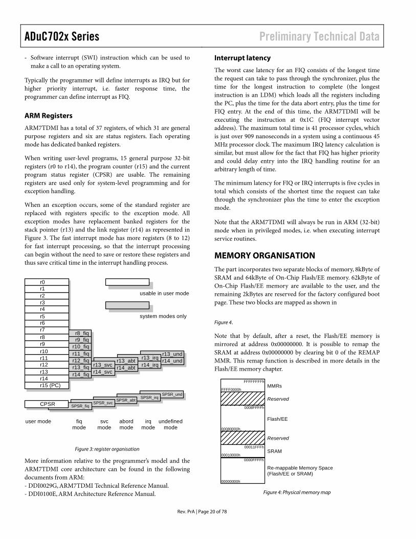
When an exception occurs, some of the standard register are replaced with registers specific to the exception mode. All exception modes have replacement banked registers for the stack pointer (r13) and the link register (r14) as represented in Figure 3. The fast interrupt mode has more registers (8 to 12) for fast interrupt processing, so that the interrupt processing can begin without the need to save or restore these registers and thus save critical time in the interrupt handling process.
Figure 3: register organisation
More information relative to the programmer’s model and the ARM7TDMI core architecture can be found in the following documents from ARM: - DDI0029G, ARM7TDMI Technical Reference Manual. - DDI0100E, ARM Architecture Reference Manual.
Interrupt latency
The worst case latency for an FIQ consists of the longest time the request can take to pass through the synchronizer, plus the time for the longest instruction to complete (the longest instruction is an LDM) which loads all the registers including the PC, plus the time for the data abort entry, plus the time for FIQ entry. At the end of this time, the ARM7TDMI will be executing the instruction at 0x1C (FIQ interrupt vector address). The maximum total time is 41 processor cycles, which is just over 909 nanoseconds in a system using a continuous 45 MHz processor clock. The maximum IRQ latency calculation is similar, but must allow for the fact that FIQ has higher priority and could delay entry into the IRQ handling routine for an arbitrary length of time.
The minimum latency for FIQ or IRQ interrupts is five cycles in total which consists of the shortest time the request can take through the synchronizer plus the time to enter the exception mode.
Note that the ARM7TDMI will always be run in ARM (32-bit) mode when in privileged modes, i.e. when executing interrupt service routines.
MEMORY ORGANISATION
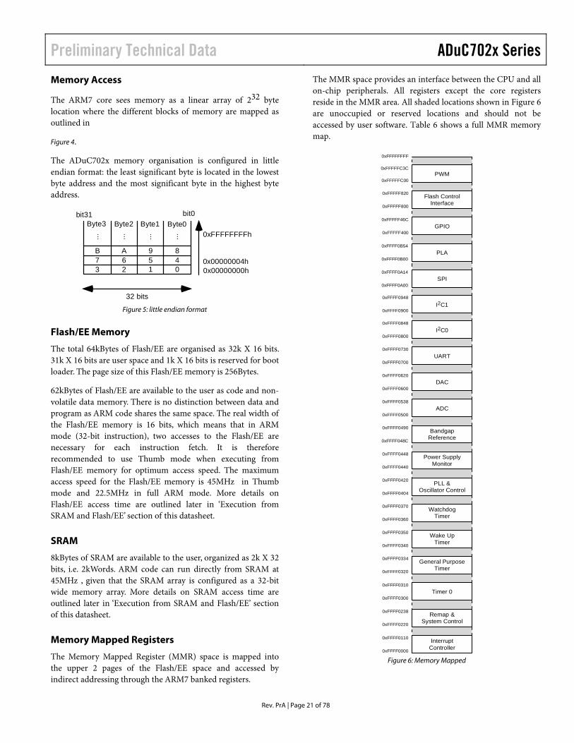
The part incorporates two separate blocks of memory, 8kByte of SRAM and 64kByte of On-Chip Flash/EE memory. 62kByte of On-Chip Flash/EE memory are available to the user, and the remaining 2kBytes are reserved for the factory configured boot page. These two blocks are mapped as shown in
Figure 4.
Note that by default, after a reset, the Flash/EE memory is mirrored at address 0x00000000. It is possible to remap the SRAM at address 0x00000000 by clearing bit 0 of the REMAP MMR. This remap function is described in more details in the Flash/EE memory chapter.
Re-mappable Memory Space(Flash/EE or SRAM)
Reserved
00080000h
Flash/EE
Reserved
00011FFFh
00010000hSRAM
FFFF0000h
FFFFFFFFhMMRs
0000FFFFh
00000000h
0008FFFFh
Figure 4: Physical memory map
user mode fiqmode
svcmode
abordmode
irqmode
undefinedmode
r0r1r2r3r4r5r6r7r8r9r10r11r12r13r14r15 (PC)
r8_fiqr9_fiq
r10_fiqr11_fiqr12_fiqr13_fiqr14_fiq
r13_svcr14_svc
r13_abtr14_abt
r13_irqr14_irq
r13_undr14_und
usable in user mode
system modes only
CPSR SPSR_fiqSPSR_svc
SPSR_undSPSR_abt SPSR_irq
Preliminary Technical Data ADuC702x Series
Rev. PrA | Page 21 of 78
Memory Access
The ARM7 core sees memory as a linear array of 232 byte location where the different blocks of memory are mapped as outlined in
Figure 4.
The ADuC702x memory organisation is configured in little endian format: the least significant byte is located in the lowest byte address and the most significant byte in the highest byte address.
Figure 5: little endian format
Flash/EE Memory
The total 64kBytes of Flash/EE are organised as 32k X 16 bits. 31k X 16 bits are user space and 1k X 16 bits is reserved for boot loader. The page size of this Flash/EE memory is 256Bytes.
62kBytes of Flash/EE are available to the user as code and non-volatile data memory. There is no distinction between data and program as ARM code shares the same space. The real width of the Flash/EE memory is 16 bits, which means that in ARM mode (32-bit instruction), two accesses to the Flash/EE are necessary for each instruction fetch. It is therefore recommended to use Thumb mode when executing from Flash/EE memory for optimum access speed. The maximum access speed for the Flash/EE memory is 45MHz in Thumb mode and 22.5MHz in full ARM mode. More details on Flash/EE access time are outlined later in ‘Execution from SRAM and Flash/EE’ section of this datasheet.
SRAM
8kBytes of SRAM are available to the user, organized as 2k X 32 bits, i.e. 2kWords. ARM code can run directly from SRAM at 45MHz , given that the SRAM array is configured as a 32-bit wide memory array. More details on SRAM access time are outlined later in ‘Execution from SRAM and Flash/EE’ section of this datasheet.
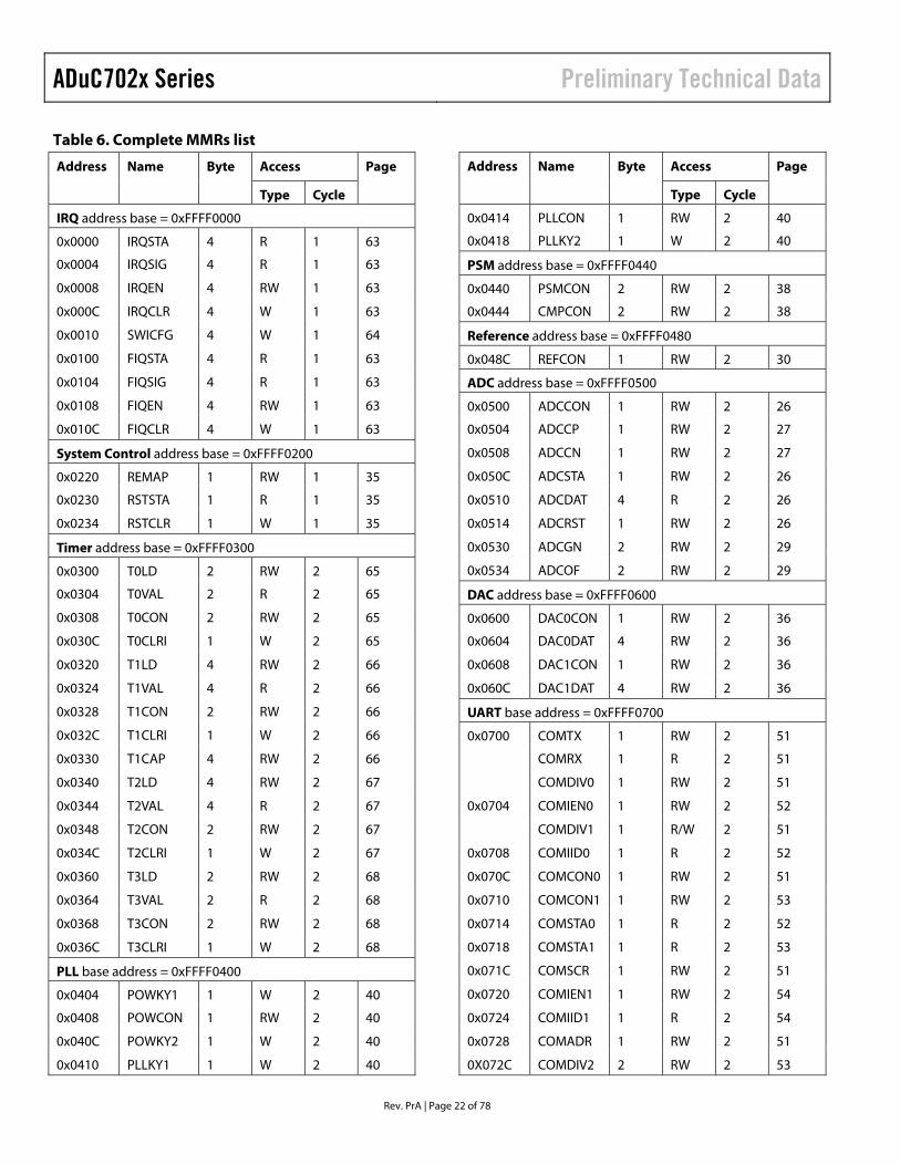
Memory Mapped Registers
The Memory Mapped Register (MMR) space is mapped into the upper 2 pages of the Flash/EE space and accessed by indirect addressing through the ARM7 banked registers.
The MMR space provides an interface between the CPU and all on-chip peripherals. All registers except the core registers reside in the MMR area. All shaded locations shown in Figure 6 are unoccupied or reserved locations and should not be accessed by user software. Table 6 shows a full MMR memory map.
InterruptController
Remap &System Control
I2C0
UART
DAC
ADC
PLA
BandgapReference
Power SupplyMonitor
GPIO
Timer 0
PLL &Oscillator Control
WatchdogTimer
Flash ControlInterface
General PurposeTimer
Wake UpTimer
0xFFFF0000
0xFFFF0110
0xFFFF0320
0xFFFF0310
0xFFFF0300
0xFFFF0238
0xFFFF0220
0xFFFF0600
0xFFFFF400
0xFFFF0B54
0xFFFF0B00
0xFFFF0A14
0xFFFF0A00
0xFFFF0848
0xFFFF0800
0xFFFF0730
0xFFFF0700
0xFFFF0620
0xFFFF0500
0xFFFF0538
0xFFFF0490
0xFFFF048C
0xFFFF0334
0xFFFF0448
0xFFFF0440
0xFFFF0420
0xFFFF0404
0xFFFF0340
0xFFFF0350
0xFFFF0360
0xFFFF0370
0xFFFFF46C
0xFFFFFFFF
0xFFFFF800
0xFFFFF820
PWM0xFFFFFC3C
0xFFFFFC00
I2C10xFFFF0948
0xFFFF0900
SPI
Figure 6: Memory Mapped
32 bits
Byte0Byte1Byte2Byte3
0x00000000h0x00000004h
bit0bit31
0123456789AB
... ... ...... 0xFFFFFFFFh
ADuC702x Series Preliminary Technical Data
Rev. PrA | Page 22 of 78
Table 6. Complete MMRs list
Access Address Name Byte
Type Cycle
Page
IRQ address base = 0xFFFF0000
0x0000 IRQSTA 4 R 1 63
0x0004 IRQSIG 4 R 1 63
0x0008 IRQEN 4 RW 1 63
0x000C IRQCLR 4 W 1 63
0x0010 SWICFG 4 W 1 64
0x0100 FIQSTA 4 R 1 63
0x0104 FIQSIG 4 R 1 63
0x0108 FIQEN 4 RW 1 63
0x010C FIQCLR 4 W 1 63
System Control address base = 0xFFFF0200
0x0220 REMAP 1 RW 1 35
0x0230 RSTSTA 1 R 1 35
0x0234 RSTCLR 1 W 1 35
Timer address base = 0xFFFF0300
0x0300 T0LD 2 RW 2 65
0x0304 T0VAL 2 R 2 65
0x0308 T0CON 2 RW 2 65
0x030C T0CLRI 1 W 2 65
0x0320 T1LD 4 RW 2 66
0x0324 T1VAL 4 R 2 66
0x0328 T1CON 2 RW 2 66
0x032C T1CLRI 1 W 2 66
0x0330 T1CAP 4 RW 2 66
0x0340 T2LD 4 RW 2 67
0x0344 T2VAL 4 R 2 67
0x0348 T2CON 2 RW 2 67
0x034C T2CLRI 1 W 2 67
0x0360 T3LD 2 RW 2 68
0x0364 T3VAL 2 R 2 68
0x0368 T3CON 2 RW 2 68
0x036C T3CLRI 1 W 2 68
PLL base address = 0xFFFF0400
0x0404 POWKY1 1 W 2 40
0x0408 POWCON 1 RW 2 40
0x040C POWKY2 1 W 2 40
0x0410 PLLKY1 1 W 2 40
Access Address Name Byte
Type Cycle
Page
0x0414 PLLCON 1 RW 2 40
0x0418 PLLKY2 1 W 2 40
PSM address base = 0xFFFF0440
0x0440 PSMCON 2 RW 2 38
0x0444 CMPCON 2 RW 2 38
Reference address base = 0xFFFF0480
0x048C REFCON 1 RW 2 30
ADC address base = 0xFFFF0500
0x0500 ADCCON 1 RW 2 26
0x0504 ADCCP 1 RW 2 27
0x0508 ADCCN 1 RW 2 27
0x050C ADCSTA 1 RW 2 26
0x0510 ADCDAT 4 R 2 26
0x0514 ADCRST 1 RW 2 26
0x0530 ADCGN 2 RW 2 29
0x0534 ADCOF 2 RW 2 29
DAC address base = 0xFFFF0600
0x0600 DAC0CON 1 RW 2 36
0x0604 DAC0DAT 4 RW 2 36
0x0608 DAC1CON 1 RW 2 36
0x060C DAC1DAT 4 RW 2 36
UART base address = 0xFFFF0700
0x0700 COMTX 1 RW 2 51
COMRX 1 R 2 51
COMDIV0 1 RW 2 51
0x0704 COMIEN0 1 RW 2 52
COMDIV1 1 R/W 2 51
0x0708 COMIID0 1 R 2 52
0x070C COMCON0 1 RW 2 51
0x0710 COMCON1 1 RW 2 53
0x0714 COMSTA0 1 R 2 52
0x0718 COMSTA1 1 R 2 53
0x071C COMSCR 1 RW 2 51
0x0720 COMIEN1 1 RW 2 54
0x0724 COMIID1 1 R 2 54
0x0728 COMADR 1 RW 2 51
0X072C COMDIV2 2 RW 2 53
Preliminary Technical Data ADuC702x Series
Rev. PrA | Page 23 of 78
Access Address Name Byte
Type Cycle
Page
I2C0 base address = 0xFFFF0800
0x0800 I2C0MSTA 1 R 2 58
0x0804 I2C0SSTA 1 R 2 58
0x0808 I2C0SRX 1 R 2 57
0x080C I2C0STX 1 W 2 57
0x0810 I2C0MRX 1 R 2 57
0x0814 I2C0MTX 1 W 2 57
0x0818 I2C0CNT 1 RW 2 57
0x081C I2C0ADR 1 RW 2 57
0x0824 I2C0BYTE 1 RW 2 57
0x0828 I2C0ALT 1 RW 2 57
0x082C I2C0CFG 1 RW 2 57
0x0830 I2C0DIVH 1 RW 2 57
0x0834 I2C0DIVL 1 RW 2 57
0x0838 I2C0ID0 1 RW 2 57
0x083C I2C0ID1 1 RW 2 57
0x0840 I2C0ID2 1 RW 2 57
0x0844 I2C0ID3 1 RW 2 57
I2C1 base address = 0xFFFF0900
0x0900 I2C1MSTA 1 R 2 58
0x0904 I2C1SSTA 1 R 2 58
0x0908 I2C1SRX 1 R 2 57
0x090C I2C1STX 1 W 2 57
0x0910 I2C1MRX 1 R 2 57
0x0914 I2C1MTX 1 W 2 57
0x0918 I2C1CNT 1 RW 2 57
0x091C I2C1ADR 1 RW 2 57
0x0924 I2C1BYTE 1 RW 2 57
0x0928 I2C1ALT 1 RW 2 57
0x092C I2C1CFG 1 RW 2 57
0x0930 I2C1DIVH 1 RW 2 57
0x0934 I2C1DIVL 1 RW 2 57
0x0938 I2C1ID0 1 RW 2 57
0x093C I2C1ID1 1 RW 2 57
0x0940 I2C1ID2 1 RW 2 57
0x0944 I2C1ID3 1 RW 2 57
SPI base address = 0xFFFF0A00
0x0A00 SPISTA 1 R 2 55
0x0A04 SPIRX 1 R 2 55
Access Address Name Byte
Type Cycle
Page
0x0A08 SPITX 1 W 2 55
0x0A0C SPIDIV 1 RW 2 55
0x0A10 SPICON 2 RW 2 55
PLA base address = 0xFFFF0B00
0x0B00 PLAELM0 2 RW 2 60
0x0B04 PLAELM1 2 RW 2 60
0x0B08 PLAELM2 2 RW 2 60
0x0B0C PLAELM3 2 RW 2 60
0x0B10 PLAELM4 2 RW 2 60
0x0B14 PLAELM5 2 RW 2 60
0x0B18 PLAELM6 2 RW 2 60
0x0B1C PLAELM7 2 RW 2 60
0x0B20 PLAELM8 2 RW 2 60
0x0B24 PLAELM9 2 RW 2 60
0x0B28 PLAELM10 2 RW 2 60
0x0B2C PLAELM11 2 RW 2 60
0x0B30 PLAELM12 2 RW 2 60
0x0B34 PLAELM13 2 RW 2 60
0x0B38 PLAELM14 2 RW 2 60
0x0B3C PLAELM15 2 RW 2 60
0x0B40 PLACLK 1 RW 2 61
0x0B44 PLAIRQ 4 RW 2 61
0x0B48 PLAADC 4 RW 2 62
0x0B4C PLADIN 4 R 2 62
0x0B50 PLADOUT 4 RW 2 62
External Memory base address = 0xFFFFF000
0xF000 XMCFG 1 RW 2
0xF010 XM0CON 1 RW 2
0xF014 XM1CON 1 RW 2
0xF018 XM2CON 1 RW 2
0xF01C XM3CON 1 RW 2
0xF020 XM0PAR 2 RW 2
0xF024 XM1PAR 2 RW 2
0xF028 XM2PAR 2 RW 2
0xF02C XM3PAR 2 RW 2
GPIO base address = 0xFFFFF400
0xF400 GP0CON 4 RW 1 48
ADuC702x Series Preliminary Technical Data
Rev. PrA | Page 24 of 78
0xF404 GP1CON 4 RW 1 48
0xF408 GP2CON 4 RW 1 48
0xF40C GP3CON 4 RW 1 48
0xF410 GP4CON 4 RW 1 48
0xF420 GP0DAT 4 RW 1 49
0xF424 GP0SET 1 W 1 49
0xF428 GP0CLR 1 W 1 49
0xF430 GP1DAT 4 RW 1 49
0xF434 GP1SET 1 W 1 49
0xF438 GP1CLR 1 W 1 49
0xF440 GP2DAT 4 RW 1 49
0xF444 GP2SET 1 W 1 49
Access Address Name Byte
Type Cycle
Page
0xF448 GP2CLR 1 W 1 49
0xF450 GP3DAT 4 RW 1 49
0xF454 GP3SET 1 W 1 49
0xF458 GP3CLR 1 W 1 49
0xF460 GP4DAT 4 RW 1 49
0xF464 GP4SET 1 W 1 49
0xF468 GP4CLR 1 W 1 49
Flash/EE base address = 0xFFFFF800
0xF800 FEESTA 1 R 1 32
0xF804 FEEMOD 1 RW 1 32
0xF808 FEECON 1 RW 1 32
0xF80C FEEDAT 2 RW 1 32
0xF810 FEEADR 2 RW 1 32
0xF818 FEESIGN 3 R 1 32
0xF81C FEEPRO 4 RW 1 33
0xF820 FEEHIDE 4 RW 1 33
PWM base address= 0xFFFFFC00
0xFC00 PWMCON 2 RW 1 46
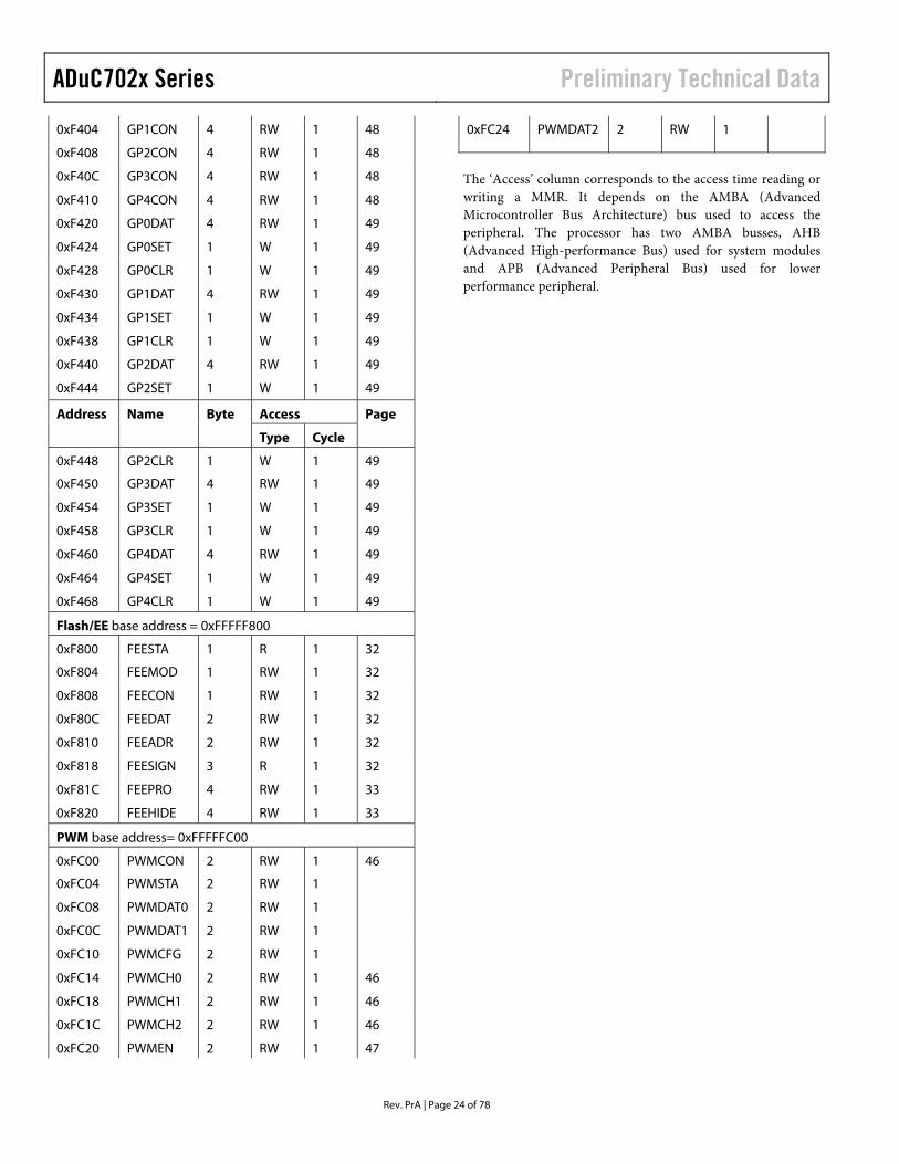
0xFC04 PWMSTA 2 RW 1
0xFC08 PWMDAT0 2 RW 1
0xFC0C PWMDAT1 2 RW 1
0xFC10 PWMCFG 2 RW 1
0xFC14 PWMCH0 2 RW 1 46
0xFC18 PWMCH1 2 RW 1 46
0xFC1C PWMCH2 2 RW 1 46
0xFC20 PWMEN 2 RW 1 47
0xFC24 PWMDAT2 2 RW 1
The ‘Access’ column corresponds to the access time reading or writing a MMR. It depends on the AMBA (Advanced Microcontroller Bus Architecture) bus used to access the peripheral. The processor has two AMBA busses, AHB (Advanced High-performance Bus) used for system modules and APB (Advanced Peripheral Bus) used for lower performance peripheral.
Preliminary Technical Data ADuC702x Series
Rev. PrA | Page 25 of 78
ADC CIRCUIT INFORMATION GENERAL OVERVIEW
The Analog Digital Converter (ADC) incorporates a fast, multi-channel, 12-bit ADC. It can operate from 2.7V to 3.6V supplies and is capable of providing a throughput of up to 1MSPS when the clock source is 45MHz. This block provides the user with multi-channel multiplexer, differential track-and-hold, on-chip reference and ADC.
The ADC consists of a 12-bit successive-approximation converter based around two capacitor DACs. It can operate in one of three different modes, depending on the input signal configuration :
• fully differential mode, for small and balanced signals • single-ended mode, for any single-ended signals • pseudo-differential mode, for any single-ended signals,
taking advantage of the common mode rejection offered by the pseudo differential input.
The converter accepts an analog input range of 0 to VREF when operating in single-ended mode or pseudo-differential mode. In fully differential mode, the input signal must be balanced around a common mode voltage VCM, in the range 0V to AVDD and with a maximum amplitude of 2 VREF (see Figure 7).
Figure 7: examples of balanced signals for fully differential mode
A high precision, low drift, and factory calibrated 2.5 V reference is provided on-chip. An external reference can also be connected as described later.
Single or continuous conversion modes can be initiated in software. An external CONVSTART pin, an output generated from the on-chip PLA or a Timer1 or a Timer2 overflow can also be used to generate a repetitive trigger for ADC conversions. A voltage output from an on-chip bandgap reference proportional to absolute temperature can also be routed through the front end ADC multiplexer (effectively an additional ADC channel input) facilitating an internal temperature sensor channel, measuring die temperature to an accuracy of ±3°C.
ADC TRANSFER FUNCTION
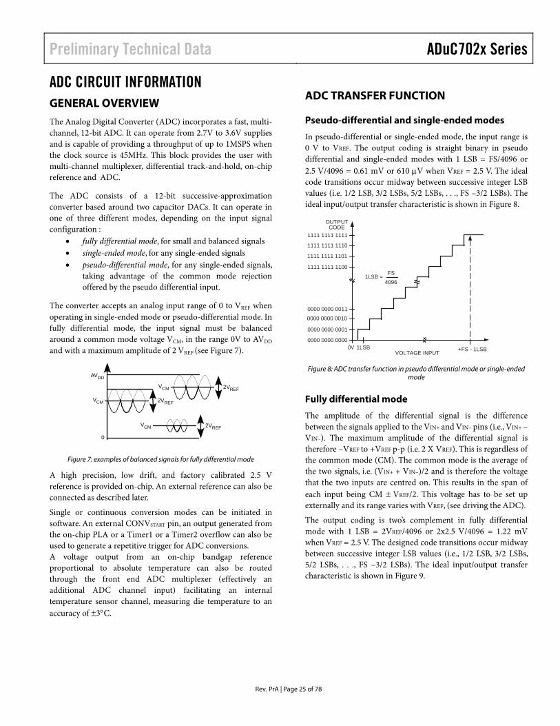
Pseudo-differential and single-ended modes
In pseudo-differential or single-ended mode, the input range is 0 V to VREF. The output coding is straight binary in pseudo differential and single-ended modes with 1 LSB = FS/4096 or 2.5 V/4096 = 0.61 mV or 610 µV when VREF = 2.5 V. The ideal code transitions occur midway between successive integer LSB values (i.e. 1/2 LSB, 3/2 LSBs, 5/2 LSBs, . . ., FS –3/2 LSBs). The ideal input/output transfer characteristic is shown in Figure 8.
OUTPUTCODE
1111 1111 1111
1111 1111 1110
1111 1111 1101
1111 1111 1100
0000 0000 0011
0000 0000 0010
0000 0000 0001
0000 0000 00000V 1LSB +FS - 1LSB
VOLTAGE INPUT
1LSB =FS
4096
Figure 8: ADC transfer function in pseudo differential mode or single-ended
mode
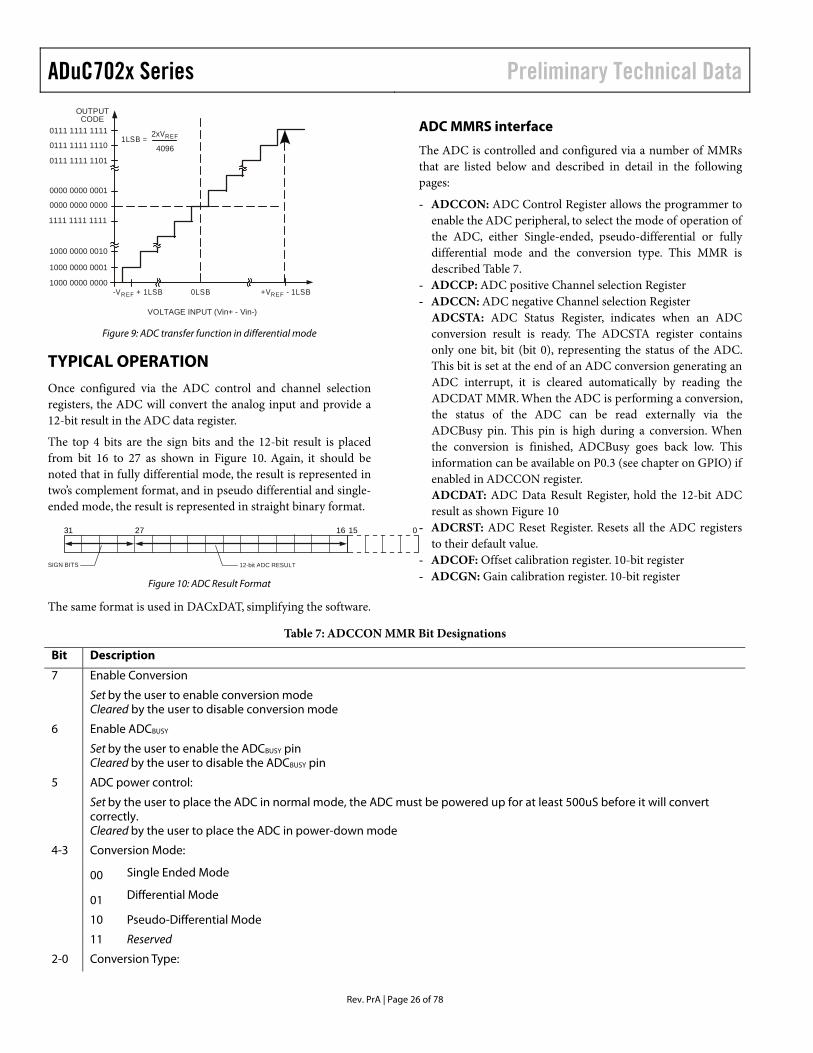
Fully differential mode
The amplitude of the differential signal is the difference between the signals applied to the VIN+ and VIN– pins (i.e., VIN+ – VIN–). The maximum amplitude of the differential signal is therefore –VREF to +VREF p-p (i.e. 2 X VREF). This is regardless of the common mode (CM). The common mode is the average of the two signals, i.e. (VIN+ + VIN–)/2 and is therefore the voltage that the two inputs are centred on. This results in the span of each input being CM ± VREF/2. This voltage has to be set up externally and its range varies with VREF, (see driving the ADC).
The output coding is two’s complement in fully differential mode with 1 LSB = 2VREF/4096 or 2x2.5 V/4096 = 1.22 mV when VREF = 2.5 V. The designed code transitions occur midway between successive integer LSB values (i.e., 1/2 LSB, 3/2 LSBs, 5/2 LSBs, . . ., FS –3/2 LSBs). The ideal input/output transfer characteristic is shown in Figure 9.
VCM 2VREF
VCM 2VREF
VCM 2VREF
AVDD
0
ADuC702x Series Preliminary Technical Data
Rev. PrA | Page 26 of 78
OUTPUTCODE
0111 1111 1111
0111 1111 1110
0111 1111 1101
1000 0000 0010
1000 0000 0001
1000 0000 0000-VREF + 1LSB
VOLTAGE INPUT (Vin+ - Vin-)
1LSB =2xVREF
4096
+VREF - 1LSB0LSB
0000 0000 0001
0000 0000 0000
1111 1111 1111
Figure 9: ADC transfer function in differential mode
TYPICAL OPERATION
Once configured via the ADC control and channel selection registers, the ADC will convert the analog input and provide a 12-bit result in the ADC data register.
The top 4 bits are the sign bits and the 12-bit result is placed from bit 16 to 27 as shown in Figure 10. Again, it should be noted that in fully differential mode, the result is represented in two’s complement format, and in pseudo differential and single-ended mode, the result is represented in straight binary format.
12-bit ADC RESULTSIGN BITS
1516 02731
Figure 10: ADC Result Format
The same format is used in DACxDAT, simplifying the software.
ADC MMRS interface
The ADC is controlled and configured via a number of MMRs that are listed below and described in detail in the following pages:
- ADCCON: ADC Control Register allows the programmer to enable the ADC peripheral, to select the mode of operation of the ADC, either Single-ended, pseudo-differential or fully differential mode and the conversion type. This MMR is described Table 7.
- ADCCP: ADC positive Channel selection Register - ADCCN: ADC negative Channel selection Register
ADCSTA: ADC Status Register, indicates when an ADC conversion result is ready. The ADCSTA register contains only one bit, bit (bit 0), representing the status of the ADC. This bit is set at the end of an ADC conversion generating an ADC interrupt, it is cleared automatically by reading the ADCDAT MMR. When the ADC is performing a conversion, the status of the ADC can be read externally via the ADCBusy pin. This pin is high during a conversion. When the conversion is finished, ADCBusy goes back low. This information can be available on P0.3 (see chapter on GPIO) if enabled in ADCCON register. ADCDAT: ADC Data Result Register, hold the 12-bit ADC result as shown Figure 10
- ADCRST: ADC Reset Register. Resets all the ADC registers to their default value.
- ADCOF: Offset calibration register. 10-bit register - ADCGN: Gain calibration register. 10-bit register
Table 7: ADCCON MMR Bit Designations
Bit Description
7 Enable Conversion
Set by the user to enable conversion mode Cleared by the user to disable conversion mode
6 Enable ADCBUSY
Set by the user to enable the ADCBUSY pin Cleared by the user to disable the ADCBUSY pin
5 ADC power control:
Set by the user to place the ADC in normal mode, the ADC must be powered up for at least 500uS before it will convert correctly. Cleared by the user to place the ADC in power-down mode
Conversion Mode:
00 Single Ended Mode
01 Differential Mode
10 Pseudo-Differential Mode
4-3
11 Reserved
2-0 Conversion Type:
Preliminary Technical Data ADuC702x Series
Rev. PrA | Page 27 of 78
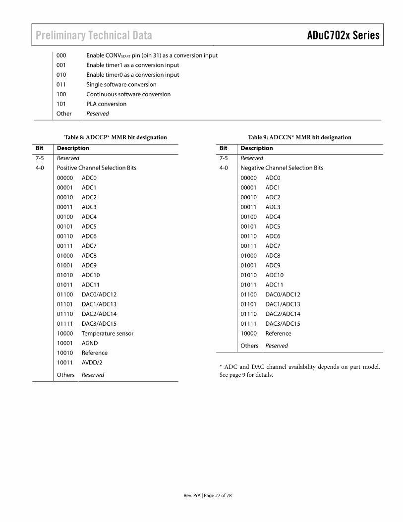
000 Enable CONVSTART pin (pin 31) as a conversion input
001 Enable timer1 as a conversion input
010 Enable timer0 as a conversion input
011 Single software conversion
100 Continuous software conversion
101 PLA conversion
Other Reserved
Table 8: ADCCP* MMR bit designation
Bit Description
7-5 Reserved
Positive Channel Selection Bits 4-0
00000
00001
00010
00011
00100
00101
00110
00111
01000
01001
01010
01011
01100
01101
01110
01111
10000
10001
10010
10011
Others
ADC0
ADC1
ADC2
ADC3
ADC4
ADC5
ADC6
ADC7
ADC8
ADC9
ADC10
ADC11
DAC0/ADC12
DAC1/ADC13
DAC2/ADC14
DAC3/ADC15
Temperature sensor
AGND
Reference
AVDD/2
Reserved
Table 9: ADCCN* MMR bit designation
Bit Description
7-5 Reserved
Negative Channel Selection Bits 4-0
00000
00001
00010
00011
00100
00101
00110
00111
01000
01001
01010
01011
01100
01101
01110
01111
10000
Others
ADC0
ADC1
ADC2
ADC3
ADC4
ADC5
ADC6
ADC7
ADC8
ADC9
ADC10
ADC11
DAC0/ADC12
DAC1/ADC13
DAC2/ADC14
DAC3/ADC15
Reference
Reserved
* ADC and DAC channel availability depends on part model. See page 9 for details.
ADuC702x Series Preliminary Technical Data
Rev. PrA | Page 28 of 78
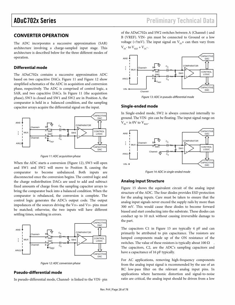
CONVERTER OPERATION
The ADC incorporates a successive approximation (SAR) architecture involving a charge-sampled input stage. This architecture is described below for the three different modes of operation.
Differential mode
The ADuC702x contains a successive approximation ADC based on two capacitive DACs. Figure 11 and Figure 12 show simplified schematics of the ADC in acquisition and conversion phase, respectively. The ADC is comprised of control logic, a SAR, and two capacitive DACs. In Figure 11 (the acquisition phase), SW3 is closed and SW1 and SW2 are in Position A, the comparator is held in a balanced condition, and the sampling capacitor arrays acquire the differential signal on the input.
Cs
Cs
A
B
AB
Channel+
Channel-
CAPACITIVEDAC
CAPACITIVEDAC
MUX CONTROLLOGIC
COMPARATORAIN0
AIN11
... SW3SW2SW1
VREF
Figure 11: ADC acquisition phase
When the ADC starts a conversion (Figure 12), SW3 will open and SW1 and SW2 will move to Position B, causing the comparator to become unbalanced. Both inputs are disconnected once the conversion begins. The control logic and the charge redistribution DACs are used to add and subtract fixed amounts of charge from the sampling capacitor arrays to bring the comparator back into a balanced condition. When the comparator is rebalanced, the conversion is complete. The control logic generates the ADC’s output code. The output impedances of the sources driving the VIN+ and VIN– pins must be matched; otherwise, the two inputs will have different settling times, resulting in errors.
Cs
Cs
A
B
AB
VREF
Channel+
Channel-
CAPACITIVEDAC
CAPACITIVEDAC
MUX CONTROLLOGIC
COMPARATORAIN0
AIN11
... SW3SW2SW1
Figure 12: ADC conversion phase
Pseudo-differential mode
In pseudo-differential mode, Channel- is linked to the VIN- pin
of the ADuC702x and SW2 switches between A (Channel-) and B (VREF). VIN- pin must be connected to Ground or a low voltage (<?mV). The input signal on VIN+ can then vary from VIN- to VREF + VIN-.
Cs
Cs
A
B
AB
Channel+
Channel-
CAPACITIVEDAC
CAPACITIVEDAC
MUXCONTROL
LOGIC
COMPARATOR
AIN0
AIN11
...
SW3SW2SW1
VREF
VIN-
Figure 13: ADC in pseudo-differential mode
Single-ended mode
In Single-ended mode, SW2 is always connected internally to ground. The VIN- pin can be floating. The input signal range on VIN+ is 0V to VREF.
Cs
Cs
A
BChannel+
Channel-
CAPACITIVEDAC
CAPACITIVEDAC
MUXCONTROL
LOGIC
COMPARATOR
AIN0
AIN11
...
SW3SW1
VIN-
Figure 14: ADC in single-ended mode
Analog Input Structure
Figure 15 shows the equivalent circuit of the analog input structure of the ADC. The four diodes provides ESD protection for the analog inputs. Care must be taken to ensure that the analog input signals never exceed the supply rails by more than 300 mV. This would cause these diodes to become forward biased and start conducting into the substrate. These diodes can conduct up to 10 mA without causing irreversible damage to the part.
The capacitors C1 in Figure 15 are typically 4 pF and can primarily be attributed to pin capacitance. The resistors are lumped components made up of the ON resistance of the switches. The value of these resistors is typically about 100 Ω . The capacitors, C2, are the ADC’s sampling capacitors and have a capacitance of 16 pF typically.
For AC applications, removing high-frequency components from the analog input signal is recommended by the use of an RC low-pass filter on the relevant analog input pins. In applications where harmonic distortion and signal-to-noise ratio are critical, the analog input should be driven from a low
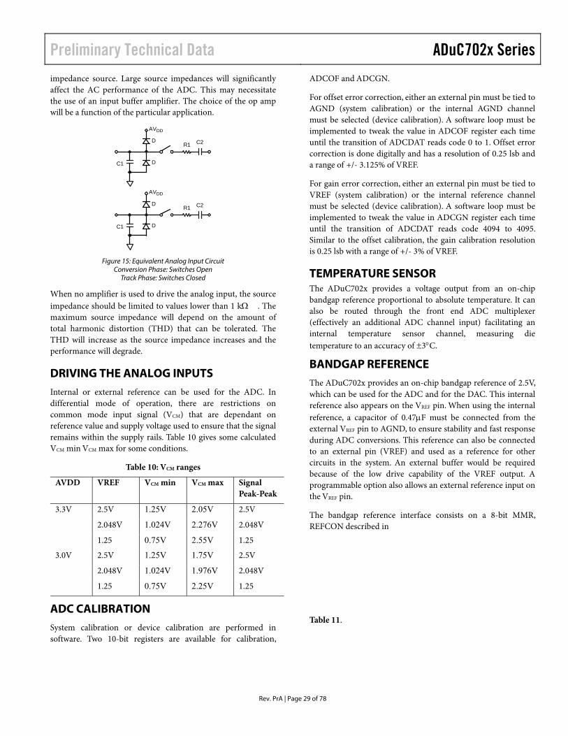
Preliminary Technical Data ADuC702x Series
Rev. PrA | Page 29 of 78
impedance source. Large source impedances will significantly affect the AC performance of the ADC. This may necessitate the use of an input buffer amplifier. The choice of the op amp will be a function of the particular application.
DC1
D
AVDD
R1 C2
DC1
D
AVDD
R1 C2
Figure 15: Equivalent Analog Input Circuit
Conversion Phase: Switches Open Track Phase: Switches Closed
When no amplifier is used to drive the analog input, the source impedance should be limited to values lower than 1 kΩ . The maximum source impedance will depend on the amount of total harmonic distortion (THD) that can be tolerated. The THD will increase as the source impedance increases and the performance will degrade.
DRIVING THE ANALOG INPUTS
Internal or external reference can be used for the ADC. In differential mode of operation, there are restrictions on common mode input signal (VCM) that are dependant on reference value and supply voltage used to ensure that the signal remains within the supply rails. Table 10 gives some calculated VCM min VCM max for some conditions.
Table 10: VCM ranges
AVDD VREF VCM min VCM max Signal Peak-Peak
2.5V 1.25V 2.05V 2.5V
2.048V 1.024V 2.276V 2.048V
3.3V
1.25 0.75V 2.55V 1.25
2.5V 1.25V 1.75V 2.5V
2.048V 1.024V 1.976V 2.048V
3.0V
1.25 0.75V 2.25V 1.25
ADC CALIBRATION
System calibration or device calibration are performed in software. Two 10-bit registers are available for calibration,
ADCOF and ADCGN.
For offset error correction, either an external pin must be tied to AGND (system calibration) or the internal AGND channel must be selected (device calibration). A software loop must be implemented to tweak the value in ADCOF register each time until the transition of ADCDAT reads code 0 to 1. Offset error correction is done digitally and has a resolution of 0.25 lsb and a range of +/- 3.125% of VREF.
For gain error correction, either an external pin must be tied to VREF (system calibration) or the internal reference channel must be selected (device calibration). A software loop must be implemented to tweak the value in ADCGN register each time until the transition of ADCDAT reads code 4094 to 4095. Similar to the offset calibration, the gain calibration resolution is 0.25 lsb with a range of +/- 3% of VREF.
TEMPERATURE SENSOR The ADuC702x provides a voltage output from an on-chip bandgap reference proportional to absolute temperature. It can also be routed through the front end ADC multiplexer (effectively an additional ADC channel input) facilitating an internal temperature sensor channel, measuring die temperature to an accuracy of ±3°C.
BANDGAP REFERENCE
The ADuC702x provides an on-chip bandgap reference of 2.5V, which can be used for the ADC and for the DAC. This internal reference also appears on the VREF pin. When using the internal reference, a capacitor of 0.47µF must be connected from the external VREF pin to AGND, to ensure stability and fast response during ADC conversions. This reference can also be connected to an external pin (VREF) and used as a reference for other circuits in the system. An external buffer would be required because of the low drive capability of the VREF output. A programmable option also allows an external reference input on the VREF pin.
The bandgap reference interface consists on a 8-bit MMR, REFCON described in
Table 11.
ADuC702x Series Preliminary Technical Data
Rev. PrA | Page 30 of 78
Table 11: REFCON MMR bit designations
Bit Description
7-2 Reserved
1 Internal reference output enable Cleared by user to place the internal reference in normal mode and use it for ADC conversions Set by user to place the internal reference in power-down mode and use an external reference
0 Internal reference output enable Set by user to connect the internal 2.5V reference to the VREF pin. The reference can be used for external component but will need to be buffered. Cleared by user to disconnect the reference from the VREF pin.
Preliminary Technical Data ADuC702x Series
Rev. PrA | Page 31 of 78
NONVOLATILE FLASH/EE MEMORY FLASH/EE MEMORY OVERVIEW
The ADuC702x incorporates Flash/EE memory technology on-chip to provide the user with non-volatile, in-circuit reprogrammable memory space.
Like EEPROM, Flash memory can be programmed in-system at a byte level, although it must first be erased; the erase being performed in page blocks. Thus, Flash memory is often and more correctly referred to as Flash/EE memory.
Overall, Flash/EE memory represents a step closer to the ideal memory device that includes non-volatility, in-circuit programmability, high density, and low cost. Incorporated in the ADuC702x, Flash/EE memory technology allows the user to update program code space in-circuit, without the need to replace one time programmable (OTP) devices at remote operating nodes.
FLASH/EE MEMORY AND THE ADUC702X
The ADuC702x contains a 64 kByte array of Flash/EE Memory. The lower 62 Kbytes is available to the user and the upper 2 kBytes of this Flash/EE program memory array contain permanently embedded firmware, allowing in circuit serial download. These 2 Kbytes of embedded firmware also contain a power-on configuration routine that downloads factory calibrated coefficients to the various calibrated peripherals (ADC, temperature sensor, bandgap references and so on). This 2 kByte embedded firmware is hidden from user code.
The 62kBytes of Flash/EE memory can be programmed in-circuit, using the serial download mode or the JTAG mode provided or via parallel programming.
(1) Serial Downloading (In-Circuit Programming)
The ADuC702x facilitates code download via the standard UART serial port or via the I2C port. The ADuC702x will enter serial download mode after a reset or power cycle if the BM pin is pulled low through an external 1kOhm resistor. Once in serial download mode, the user can download code to the full 62kBytes of Flash/EE memory while the device is in circuit in its target application hardware. A PC serial download executable is provided as part of the development system for serial downloading via the UART. An application note is available at www.analog.com/microconverter describing the protocol for serial downloading via the UART and I2C.
(2) Parallel Programming
The parallel programming protocol allows the on-chip Flash/EE memory be programmed by industry standard third party programmers.
(3) JTAG access
The JTAG protocol uses the on-chip JTAG interface to facilitate code download and debug.
FLASH/EE MEMORY SECURITY
The 62kByte of Flash/EE memory available to the user can be read and write protected.
Bit 31 of the FEEPRO/FEEHIDE MMR protects the 62kBytes from being read through JTAG and also in parallel programming mode. The other 31 bits of this register protect in writing, each bit protects 4 pages, i.e. 2kBytes. Write protection is activated for all type of access.
There are two levels of protection:
- Protection can be set and removed by writing directly into FEEHIDE MMR. - FEEPRO can be protected by a key to avoid direct access to FEEPRO. The key is saved once and must be entered again to modify FEEPRO. After three unsuccessful attempts to access FEEPRO with an invalid key, a mass erase will occur. A mass erase will set the key back to 0xFFFF but will also erase all the user code.
Sequence to write the key:
1. Enter an address in FEEADR. 2. Do a single READ command, wait for the read to be successful by monitoring FEESTA. 3. Run a verify command. 4. Write the bit in FEEPRO corresponding to the page to be protected. 5. Enable key protection by setting bits 7 to 4 of FEEMOD. 6. Write a 32 bit key in FEEADR, FEEDAT 7. Run the write key command 0x0C in FEECON, wait for the read to be successful by monitoring FEESTA.
To remove or modify the protection the same sequence can be used with a modified value of FEEPRO.
The sequence above is illustrated in the following example, this protects writing pages 4 to 7 of the FLASH:
FEEADR = 0x800; //Any address, FEECON=0x01; //Read command while (!(FEESTA & 0x01)) //Wait for read FEECON=0x04; //Verify Command FEEPRO=0xFFFFFFFD; //Protect pages 4 to 7 FEEMOD=(FEEMOD & 0xF0); //Write key enable FEEADR=0xAA55; //16 bit key value FEEDAT=0xAA55; //16 bit key value FEECON= 0x0C; // Write key command while (!(FEESTA & 0x01)) //Wait for command
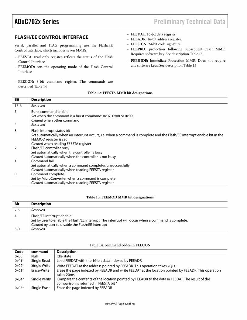
ADuC702x Series Preliminary Technical Data
Rev. PrA | Page 32 of 78
FLASH/EE CONTROL INTERFACE
Serial, parallel and JTAG programming use the Flash/EE Control Interface, which includes seven MMRs:
- FEESTA: read only register, reflects the status of the Flash Control Interface
- FEEMOD: sets the operating mode of the Flash Control Interface
- FEECON: 8-bit command register. The commands are
described Table 14
- FEEDAT: 16-bit data register. - FEEADR: 16-bit address register. - FEESIGN: 24-bit code signature - FEEPRO: protection following subsequent reset MMR.
Requires software key. See description Table 15
- FEEHIDE: Immediate Protection MMR. Does not require any software keys. See description Table 15
Table 12: FEESTA MMR bit designations
Bit Description
15-6 Reserved
5 Burst command enable Set when the command is a burst command: 0x07, 0x08 or 0x09 Cleared when other command
4 Reserved
3 Flash interrupt status bit Set automatically when an interrupt occurs, i.e. when a command is complete and the Flash/EE interrupt enable bit in the FEEMOD register is set Cleared when reading FEESTA register
2 Flash/EE controller busy Set automatically when the controller is busy Cleared automatically when the controller is not busy
1 Command fail Set automatically when a command completes unsuccessfully Cleared automatically when reading FEESTA register
0 Command complete Set by MicroConverter when a command is complete Cleared automatically when reading FEESTA register
Table 13: FEEMOD MMR bit designations
Bit Description
7-5 Reserved
4 Flash/EE interrupt enable: Set by user to enable the Flash/EE interrupt. The interrupt will occur when a command is complete. Cleared by user to disable the Flash/EE interrupt
3-0 Reserved
Table 14: command codes in FEECON
Code command Description 0x00* Null Idle state 0x01* Single Read Load FEEDAT with the 16-bit data indexed by FEEADR 0x02* Single Write Write FEEDAT at the address pointed by FEEADR. This operation takes 20µs. 0x03* Erase-Write Erase the page indexed by FEEADR and write FEEDAT at the location pointed by FEEADR. This operation
takes 20ms 0x04* Single Verify Compare the contents of the location pointed by FEEADR to the data in FEEDAT. The result of the
comparison is returned in FEESTA bit 1 0x05* Single Erase Erase the page indexed by FEEADR
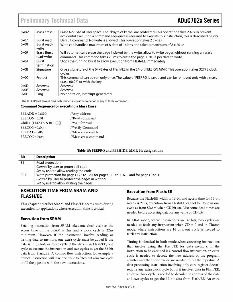
Preliminary Technical Data ADuC702x Series
Rev. PrA | Page 33 of 78
0x06* Mass erase Erase 62kByte of user space. The 2kByte of kernel are protected. This operation takes 2.48s To prevent accidental execution a command sequence is required to execute this instruction, this is described below.
0x07 Burst read Default command. No write is allowed. This operation takes 2 cycles 0x08 Burst read-
write Write can handle a maximum of 8 data of 16 bits and takes a maximum of 8 x 20 µs
0x09 Erase Burst read-write
Will automatically erase the page indexed by the write, allow to write pages without running an erase command. This command takes 20 ms to erase the page + 20 µs per data to write
0x0A Burst termination
Stops the running burst to allow execution from Flash/EE immediately
0x0B Signature Give a signature of the 64kBytes of Flash/EE in the 24-bit FEESIGN MMR. This operation takes 32778 clock cycles.
0x0C Protect This command can be run only once. The value of FEEPRO is saved and can be removed only with a mass erase (0x06) or with the key
0x0D Reserved Reserved 0x0E Reserved Reserved 0x0F Ping No operation, interrupt generated
* The FEECON will always read 0x07 immediately after execution of any of these commands.
Command Sequence for executing a Mass Erase
FEEADR = 0x800; //Any address FEECON=0x01; //Read command while (!(FEESTA & 0x01)) //Wait for read FEECON=0x04; //Verify Command FEEDAT=0x06; //Mass erase enable FEECON=0x06; //Mass erase command
Table 15: FEEPRO and FEEHIDE MMR bit designations
Bit Description
31 Read protection Cleared by user to protect all code Set by user to allow reading the code
30-0 Write protection for pages 123 to 120, for pages 119 to 116… and for pages 0 to 3 Cleared by user to protect the pages in writing Set by user to allow writing the pages
EXECUTION TIME FROM SRAM AND FLASH/EE
This chapter describes SRAM and Flash/EE access times during execution for applications where execution time is critical.
Execution from SRAM
Fetching instruction from SRAM takes one clock cycle as the access time of the SRAM is 2ns and a clock cycle is 22ns minimum. However, if the instruction involve reading or writing data to memory, one extra cycle must be added if the data is in SRAM, or three cycle if the data is in Flash/EE, one cycle to execute the instruction and two cycles to get the 32-bit data from Flash/EE. A control flow instruction, for example a branch instruction will take one cycle to fetch but also two cycle to fill the pipeline with the new instructions.
Execution from Flash/EE
Because the Flash/EE width is 16-bit and access time for 16-bit words is 22ns, execution from Flash/EE cannot be done in one cycle as from SRAM when CD bit =0. Also some dead times are needed before accessing data for any value of CD bits.
In ARM mode, where instructions are 32 bits, two cycles are needed to fetch any instruction when CD = 0 and in Thumb mode, where instructions are 16 bits, one cycle is needed to fetch any instruction.
Timing is identical in both mode when executing instructions that involve using the Flash/EE for data memory. If the instruction to be executed is a control flow instruction, an extra cycle is needed to decode the new address of the program counter and then four cycles are needed to fill the pipe-line. A data processing instruction involving only core register doesn’t require any extra clock cycle but if it involves data in Flash/EE, an extra clock cycle is needed to decode the address of the data and two cycles to get the 32-bit data from Flash/EE. An extra
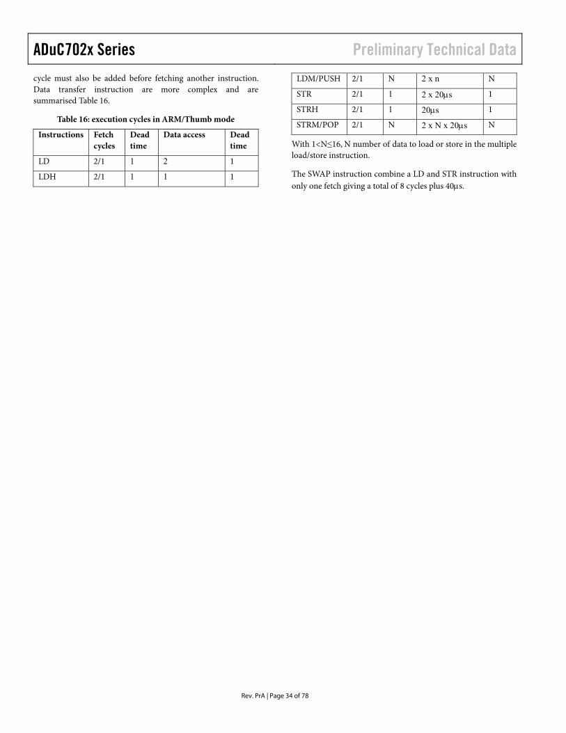
ADuC702x Series Preliminary Technical Data
Rev. PrA | Page 34 of 78
cycle must also be added before fetching another instruction. Data transfer instruction are more complex and are summarised Table 16.
Table 16: execution cycles in ARM/Thumb mode
Instructions Fetch cycles
Dead time
Data access Dead time
LD 2/1 1 2 1
LDH 2/1 1 1 1
LDM/PUSH 2/1 N 2 x n N
STR 2/1 1 2 x 20µs 1
STRH 2/1 1 20µs 1
STRM/POP 2/1 N 2 x N x 20µs N
With 1<N≤16, N number of data to load or store in the multiple load/store instruction.
The SWAP instruction combine a LD and STR instruction with only one fetch giving a total of 8 cycles plus 40µs.
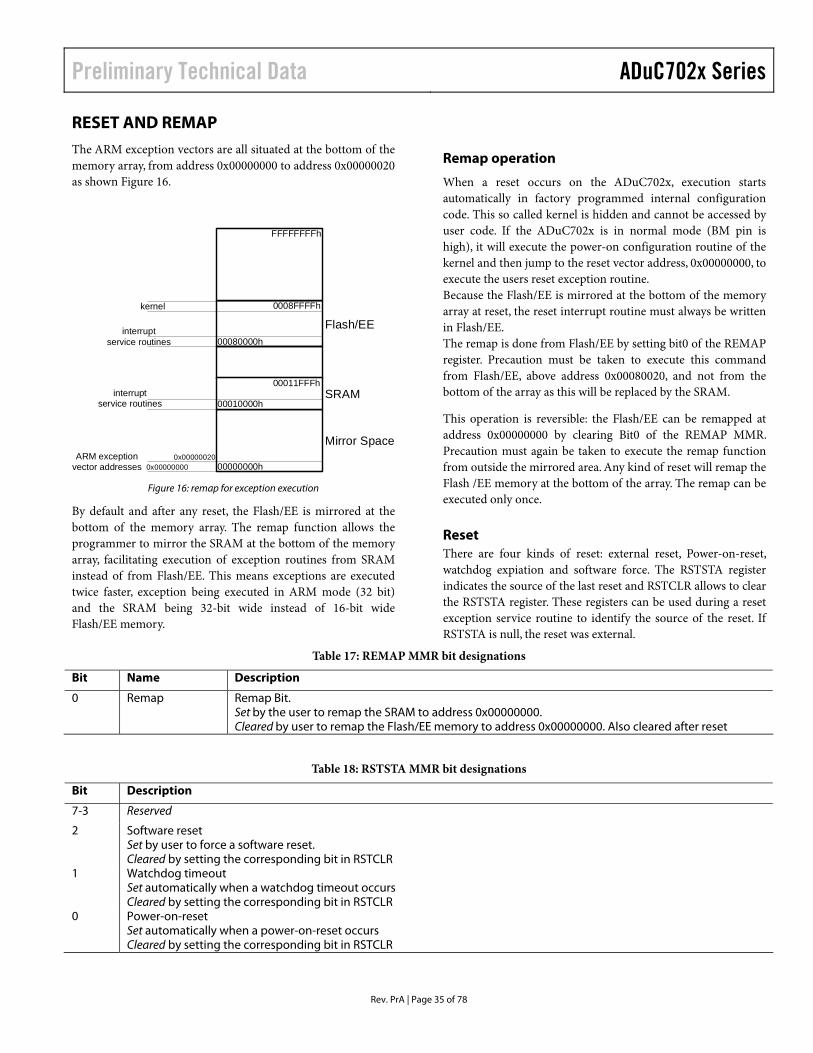
Preliminary Technical Data ADuC702x Series
Rev. PrA | Page 35 of 78
RESET AND REMAP
The ARM exception vectors are all situated at the bottom of the memory array, from address 0x00000000 to address 0x00000020 as shown Figure 16.
00000000h
Mirror Space
0008FFFFh
00080000h
Flash/EE
00011FFFh
00010000hSRAM
FFFFFFFFh
0x000000000x00000020
kernel
interruptservice routines
interruptservice routines
ARM exceptionvector addresses
Figure 16: remap for exception execution
By default and after any reset, the Flash/EE is mirrored at the bottom of the memory array. The remap function allows the programmer to mirror the SRAM at the bottom of the memory array, facilitating execution of exception routines from SRAM instead of from Flash/EE. This means exceptions are executed twice faster, exception being executed in ARM mode (32 bit) and the SRAM being 32-bit wide instead of 16-bit wide Flash/EE memory.
Remap operation
When a reset occurs on the ADuC702x, execution starts automatically in factory programmed internal configuration code. This so called kernel is hidden and cannot be accessed by user code. If the ADuC702x is in normal mode (BM pin is high), it will execute the power-on configuration routine of the kernel and then jump to the reset vector address, 0x00000000, to execute the users reset exception routine. Because the Flash/EE is mirrored at the bottom of the memory array at reset, the reset interrupt routine must always be written in Flash/EE. The remap is done from Flash/EE by setting bit0 of the REMAP register. Precaution must be taken to execute this command from Flash/EE, above address 0x00080020, and not from the bottom of the array as this will be replaced by the SRAM.
This operation is reversible: the Flash/EE can be remapped at address 0x00000000 by clearing Bit0 of the REMAP MMR. Precaution must again be taken to execute the remap function from outside the mirrored area. Any kind of reset will remap the Flash /EE memory at the bottom of the array. The remap can be executed only once.
Reset There are four kinds of reset: external reset, Power-on-reset, watchdog expiation and software force. The RSTSTA register indicates the source of the last reset and RSTCLR allows to clear the RSTSTA register. These registers can be used during a reset exception service routine to identify the source of the reset. If RSTSTA is null, the reset was external.
Table 17: REMAP MMR bit designations
Bit Name Description
0 Remap Remap Bit. Set by the user to remap the SRAM to address 0x00000000. Cleared by user to remap the Flash/EE memory to address 0x00000000. Also cleared after reset
Table 18: RSTSTA MMR bit designations
Bit Description
7-3 Reserved
2 Software reset Set by user to force a software reset. Cleared by setting the corresponding bit in RSTCLR
1 Watchdog timeout Set automatically when a watchdog timeout occurs Cleared by setting the corresponding bit in RSTCLR
0 Power-on-reset Set automatically when a power-on-reset occurs Cleared by setting the corresponding bit in RSTCLR
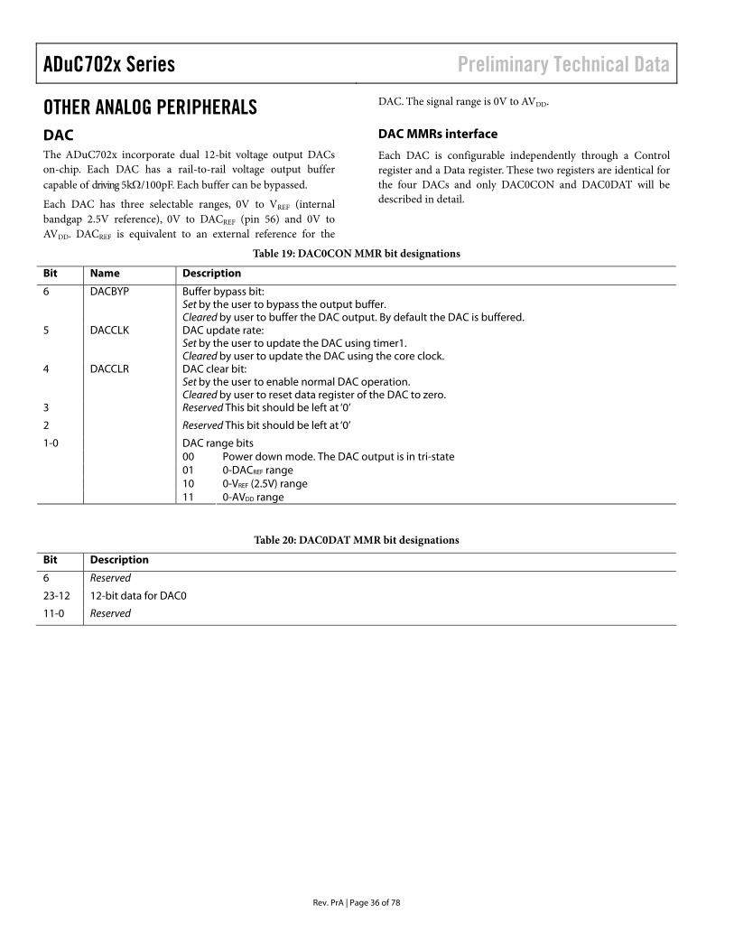
ADuC702x Series Preliminary Technical Data
Rev. PrA | Page 36 of 78
OTHER ANALOG PERIPHERALS DAC The ADuC702x incorporate dual 12-bit voltage output DACs on-chip. Each DAC has a rail-to-rail voltage output buffer capable of driving 5kΩ/100pF. Each buffer can be bypassed.
Each DAC has three selectable ranges, 0V to VREF (internal bandgap 2.5V reference), 0V to DACREF (pin 56) and 0V to AVDD. DACREF is equivalent to an external reference for the
DAC. The signal range is 0V to AVDD.
DAC MMRs interface
Each DAC is configurable independently through a Control register and a Data register. These two registers are identical for the four DACs and only DAC0CON and DAC0DAT will be described in detail.
Table 19: DAC0CON MMR bit designations
Bit Name Description
6 DACBYP Buffer bypass bit: Set by the user to bypass the output buffer. Cleared by user to buffer the DAC output. By default the DAC is buffered.
5 DACCLK DAC update rate: Set by the user to update the DAC using timer1. Cleared by user to update the DAC using the core clock.
4 DACCLR DAC clear bit: Set by the user to enable normal DAC operation. Cleared by user to reset data register of the DAC to zero.
3 Reserved This bit should be left at ‘0’
2 Reserved This bit should be left at ‘0’
DAC range bits 00 Power down mode. The DAC output is in tri-state 01 0-DACREF range 10 0-VREF (2.5V) range
1-0
11 0-AVDD range
Table 20: DAC0DAT MMR bit designations
Bit Description
6 Reserved
23-12 12-bit data for DAC0
11-0 Reserved
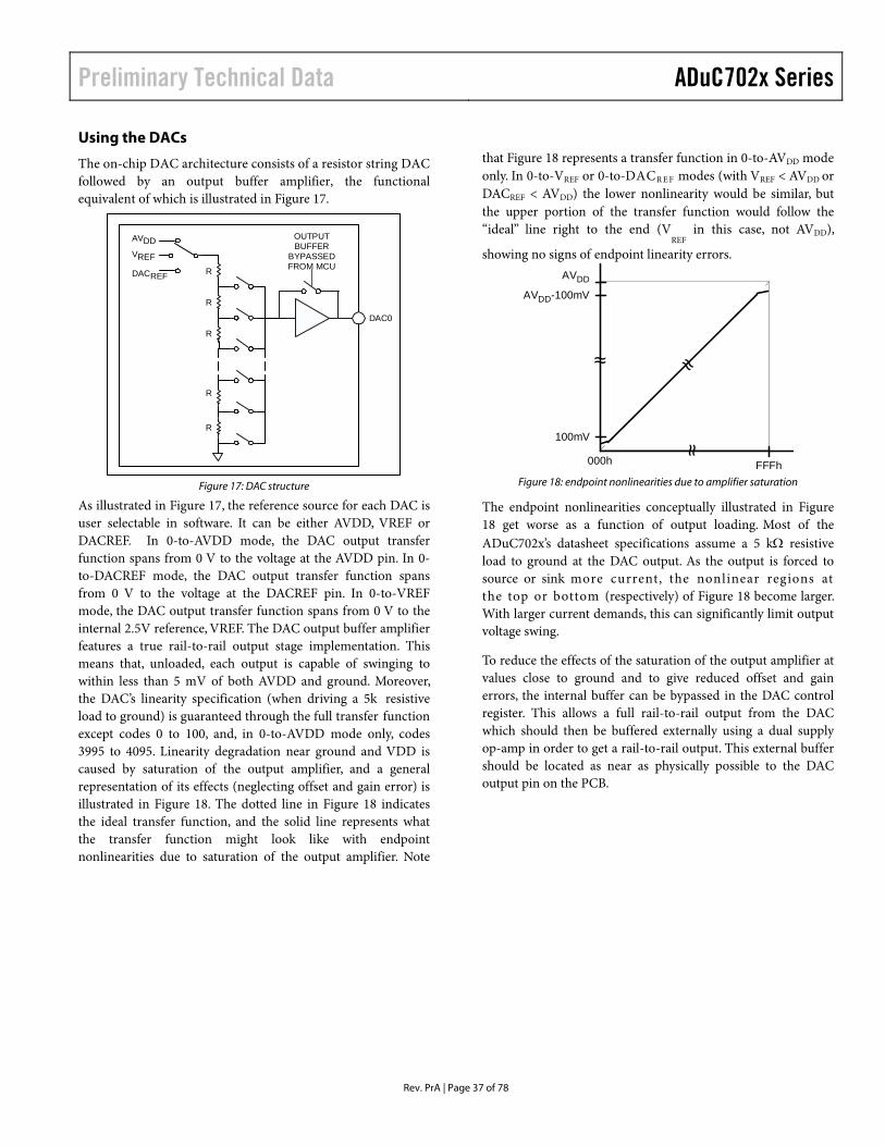
Preliminary Technical Data ADuC702x Series
Rev. PrA | Page 37 of 78
Using the DACs
The on-chip DAC architecture consists of a resistor string DAC followed by an output buffer amplifier, the functional equivalent of which is illustrated in Figure 17.
OUTPUTBUFFER
BYPASSEDFROM MCU
DAC0
R
R
R
R
R
AVDDVREF
DACREF
Figure 17: DAC structure
As illustrated in Figure 17, the reference source for each DAC is user selectable in software. It can be either AVDD, VREF or DACREF. In 0-to-AVDD mode, the DAC output transfer function spans from 0 V to the voltage at the AVDD pin. In 0-to-DACREF mode, the DAC output transfer function spans from 0 V to the voltage at the DACREF pin. In 0-to-VREF mode, the DAC output transfer function spans from 0 V to the internal 2.5V reference, VREF. The DAC output buffer amplifier features a true rail-to-rail output stage implementation. This means that, unloaded, each output is capable of swinging to within less than 5 mV of both AVDD and ground. Moreover, the DAC’s linearity specification (when driving a 5k resistive load to ground) is guaranteed through the full transfer function except codes 0 to 100, and, in 0-to-AVDD mode only, codes 3995 to 4095. Linearity degradation near ground and VDD is caused by saturation of the output amplifier, and a general representation of its effects (neglecting offset and gain error) is illustrated in Figure 18. The dotted line in Figure 18 indicates the ideal transfer function, and the solid line represents what the transfer function might look like with endpoint nonlinearities due to saturation of the output amplifier. Note
that Figure 18 represents a transfer function in 0-to-AVDD mode only. In 0-to-VREF or 0-to-DACR E F modes (with VREF < AVDD or DACREF < AVDD) the lower nonlinearity would be similar, but the upper portion of the transfer function would follow the “ideal” line right to the end (V
REF in this case, not AVDD),
showing no signs of endpoint linearity errors. AVDD
100mV
000h FFFh
AVDD-100mV
~~
~~
~~
Figure 18: endpoint nonlinearities due to amplifier saturation
The endpoint nonlinearities conceptually illustrated in Figure 18 get worse as a function of output loading. Most of the ADuC702x’s datasheet specifications assume a 5 kΩ resistive load to ground at the DAC output. As the output is forced to source or sink more current, the nonlinear regions at the top or bottom (respectively) of Figure 18 become larger. With larger current demands, this can significantly limit output voltage swing.
To reduce the effects of the saturation of the output amplifier at values close to ground and to give reduced offset and gain errors, the internal buffer can be bypassed in the DAC control register. This allows a full rail-to-rail output from the DAC which should then be buffered externally using a dual supply op-amp in order to get a rail-to-rail output. This external buffer should be located as near as physically possible to the DAC output pin on the PCB.
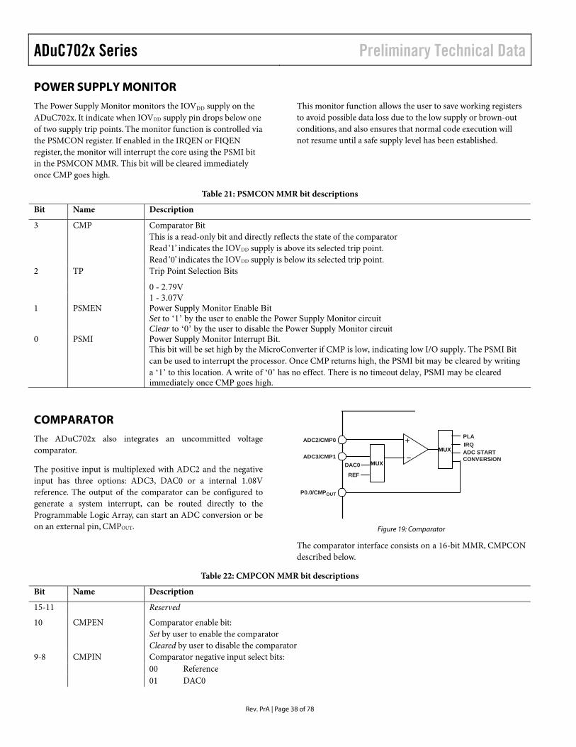
ADuC702x Series Preliminary Technical Data
Rev. PrA | Page 38 of 78
POWER SUPPLY MONITOR
The Power Supply Monitor monitors the IOVDD supply on the ADuC702x. It indicate when IOVDD supply pin drops below one of two supply trip points. The monitor function is controlled via the PSMCON register. If enabled in the IRQEN or FIQEN register, the monitor will interrupt the core using the PSMI bit in the PSMCON MMR. This bit will be cleared immediately once CMP goes high.
This monitor function allows the user to save working registers to avoid possible data loss due to the low supply or brown-out conditions, and also ensures that normal code execution will not resume until a safe supply level has been established.
Table 21: PSMCON MMR bit descriptions
Bit Name Description
3 CMP Comparator Bit This is a read-only bit and directly reflects the state of the comparator Read ‘1’ indicates the IOVDD supply is above its selected trip point. Read ‘0’ indicates the IOVDD supply is below its selected trip point. Trip Point Selection Bits
0 - 2.79V
2 TP
1 - 3.07V 1 PSMEN Power Supply Monitor Enable Bit
Set to ‘1’ by the user to enable the Power Supply Monitor circuit Clear to ‘0’ by the user to disable the Power Supply Monitor circuit
0 PSMI Power Supply Monitor Interrupt Bit. This bit will be set high by the MicroConverter if CMP is low, indicating low I/O supply. The PSMI Bit can be used to interrupt the processor. Once CMP returns high, the PSMI bit may be cleared by writing a ‘1’ to this location. A write of ‘0’ has no effect. There is no timeout delay, PSMI may be cleared immediately once CMP goes high.
COMPARATOR
The ADuC702x also integrates an uncommitted voltage comparator.
The positive input is multiplexed with ADC2 and the negative input has three options: ADC3, DAC0 or a internal 1.08V reference. The output of the comparator can be configured to generate a system interrupt, can be routed directly to the Programmable Logic Array, can start an ADC conversion or be on an external pin, CMPOUT.
MUX
ADC2/CMP0
ADC3/CMP1DAC0
REF
IRQPLA
P0.0/CMPOUT
MUX ADC STARTCONVERSION
Figure 19: Comparator
The comparator interface consists on a 16-bit MMR, CMPCON described below.
Table 22: CMPCON MMR bit descriptions
Bit Name Description
15-11 Reserved
10 CMPEN Comparator enable bit: Set by user to enable the comparator Cleared by user to disable the comparator Comparator negative input select bits: 00 Reference
9-8 CMPIN
01 DAC0
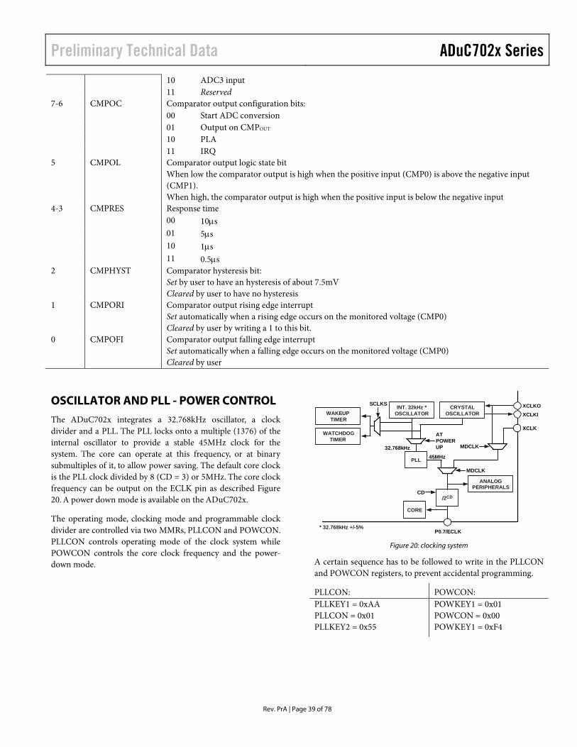
Preliminary Technical Data ADuC702x Series
Rev. PrA | Page 39 of 78
10 ADC3 input 11 Reserved Comparator output configuration bits: 00 Start ADC conversion 01 Output on CMPOUT 10 PLA
7-6 CMPOC
11 IRQ 5 CMPOL Comparator output logic state bit
When low the comparator output is high when the positive input (CMP0) is above the negative input (CMP1). When high, the comparator output is high when the positive input is below the negative input Response time 00 10µs 01 5µs 10 1µs
4-3 CMPRES
11 0.5µs 2 CMPHYST Comparator hysteresis bit:
Set by user to have an hysteresis of about 7.5mV Cleared by user to have no hysteresis
1 CMPORI Comparator output rising edge interrupt Set automatically when a rising edge occurs on the monitored voltage (CMP0) Cleared by user by writing a 1 to this bit.
0 CMPOFI Comparator output falling edge interrupt Set automatically when a falling edge occurs on the monitored voltage (CMP0) Cleared by user
OSCILLATOR AND PLL - POWER CONTROL
The ADuC702x integrates a 32.768kHz oscillator, a clock divider and a PLL. The PLL locks onto a multiple (1376) of the internal oscillator to provide a stable 45MHz clock for the system. The core can operate at this frequency, or at binary submultiples of it, to allow power saving. The default core clock is the PLL clock divided by 8 (CD = 3) or 5MHz. The core clock frequency can be output on the ECLK pin as described Figure 20. A power down mode is available on the ADuC702x.
The operating mode, clocking mode and programmable clock divider are controlled via two MMRs, PLLCON and POWCON. PLLCON controls operating mode of the clock system while POWCON controls the core clock frequency and the power-down mode.
PLL
XCLKOXCLKI
P0.7/ECLK
/2CD
XCLK
WAKEUPTIMER
WATCHDOGTIMER
INT. 32kHz *OSCILLATOR
CRYSTALOSCILLATOR
ANALOGPERIPHERALS
CORE
SCLKS
MDCLK
MDCLK
ATPOWERUP
CD
45MHz32.768kHz
* 32.768kHz +/-5% Figure 20: clocking system
A certain sequence has to be followed to write in the PLLCON and POWCON registers, to prevent accidental programming.
PLLCON: POWCON: PLLKEY1 = 0xAA PLLCON = 0x01 PLLKEY2 = 0x55
POWKEY1 = 0x01 POWCON = 0x00 POWKEY1 = 0xF4
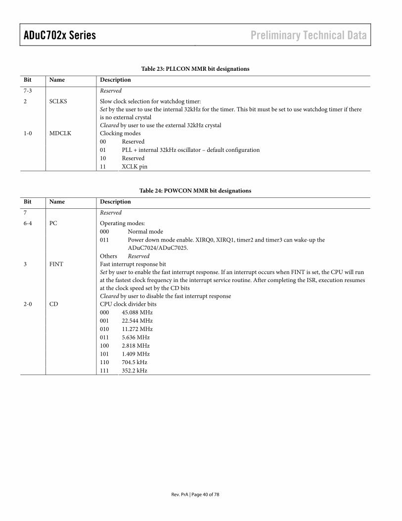
ADuC702x Series Preliminary Technical Data
Rev. PrA | Page 40 of 78
Table 23: PLLCON MMR bit designations
Bit Name Description
7-3 Reserved
2 SCLKS Slow clock selection for watchdog timer: Set by the user to use the internal 32kHz for the timer. This bit must be set to use watchdog timer if there is no external crystal Cleared by user to use the external 32kHz crystal Clocking modes 00 Reserved 01 PLL + internal 32kHz oscillator – default configuration 10 Reserved
1-0 MDCLK
11 XCLK pin
Table 24: POWCON MMR bit designations
Bit Name Description
7 Reserved
Operating modes: 000 Normal mode 011 Power down mode enable. XIRQ0, XIRQ1, timer2 and timer3 can wake-up the
ADuC7024/ADuC7025.
6-4 PC
Others Reserved 3 FINT Fast interrupt response bit
Set by user to enable the fast interrupt response. If an interrupt occurs when FINT is set, the CPU will run at the fastest clock frequency in the interrupt service routine. After completing the ISR, execution resumes at the clock speed set by the CD bits Cleared by user to disable the fast interrupt response CPU clock divider bits 000 45.088 MHz 001 22.544 MHz 010 11.272 MHz 011 5.636 MHz 100 2.818 MHz 101 1.409 MHz 110 704.5 kHz
2-0 CD
111 352.2 kHz
Preliminary Technical Data ADuC702x Series
Rev. PrA | Page 41 of 78
DIGITAL PERIPHERALS THREE-PHASE PWM
General overview
The ADuC702x provides a flexible, programmable, three-phase PWM waveform generator that can be programmed to generate the required switching patterns to drive a three-phase voltage source inverter for ac induction (ACIM) motor control.
The PWM generator produces three pairs of PWM signal on the six PWM output pins (PWM0H, PWM0L, PWM1H, PWM1L, PWM2H, and PWM2L). The six PWM output signals consist of three high-side drive signals and three low-side drive signals.
The switching frequency and dead time of the generated PWM patterns are programmable using the PWMDAT0 and PWMDAT1 MMRs. In addition, three duty-cycle control registers (PWMCH0, PWMCH1 and PWMCH2) directly control the duty cycles of the three-pairs of PWM signals.
Each of the six PWM output signals can be enabled or disabled by separate output enable bits of the PWMEN register. In addition, three control bits of the PWMEN register permit crossover of the two signals of a PWM pair. In crossover mode, the PWM signal destined for the high side switch is diverted to the complementary low side output and the signal destined for the low side switch is diverted to the corresponding high side output signal.
In many applications, there is a need to provide an isolation barrier in the gate-drive circuits that turns on the power devices of the inverter. In general, there are two common isolation techniques, optical isolation using opto-couplers and transformer isolation using pulse transformers. The PWM controller permits mixing of the output PWM signals with a high frequency chopping signal to permit easy interface to such pulse transformers. The features of this gate-drive chopping mode can be controlled by the PWMCFG register. An 8-bit value within the PWMCFG register directly controls the chopping frequency. High frequency chopping can be independently enabled for the high-side and the low-side outputs using separate control bits in the PWMCFG register.
The PWM generator is capable of operating in two distinct modes, single update mode or double update mode. In single update mode the duty cycle values are programmable only once per PWM period, so that the resultant PWM patterns are symmetrical about the midpoint of the PWM period. In the double update mode, a second updating of the PWM duty cycle values is implemented at the midpoint of the PWM period. In this mode, it is possible to produce asymmetrical PWM patterns, that produce lower harmonic distortion in three-phase PWM inverters. This technique also permits closed loop
controllers to change the average voltage applied to the machine windings at a faster rate and so permits faster closed loop bandwidths to be achieved. The operating mode of the PWM block is selected by a control bit in the PWMCON register. In single update mode a PWMSYNC pulse is produced at the start of each PWM period. In double update mode, an additional PWMSYNC pulse is produced at the midpoint of each PWM period.
The PWM block can also provide an internal synchronisation pulse on the SYNC pin that is synchronise to the PWM switching frequency. In single update mode a pulse is produce at the start of each PWM period. In double update mode, an additional pulse is also produced at the mid-point of each PWM period. The width of the pulse is programmable through the PWMDAT2 register. The PWM block can also accept an external synchronisation pulse on the SYNC pin. The selection of external synchronisation or internal synchronisation is in the PWMCON register. The SYNC input timing can be synchronised to the internal peripheral clock, which is selected in the PWMCON register. If the external synchronisation pulse from the chip pin is asynchronous to the internal peripheral clock (typical case), the external SYNC is considered asynchronous and should be synchronised. The synchronisation logic will add latency add jitter from the external pulse to the actual PWM outputs. The size of the pulse on the SYNC pin must be greater than two core clock periods.
The PWM signals produced by the ADuC702x can be shut off via a dedicated asynchronous PWM shutdown pin, PWMTRIP, that, when brought low, instantaneously places all six PWM outputs in the OFF state (high). This hardware shutdown mechanism is asynchronous so that the associated PWM disable circuitry does not go through any clocked logic, thereby ensuring correct PWM shutdown even in the event of a loss of the core clock.
Status information about the PWM system is available to the user in the PWMSTA register. In particular, the state of the PWMTRIP pin is available, as well as a status bit that indicates whether operation is in the first half or the second half of the PWM period.
Description of the PWM block
A functional block diagram of the PWM controller is shown in Figure 21. The generation of the six output PWM signals on pins PWM0H to PWM2L is controlled by four important blocks:
• The Three-Phase PWM Timing Unit, which is the core of the PWM controller. It generates three pairs of complemented and dead-time-adjusted centre-based PWM signals.
• The Output Control Unit allows the redirection of the outputs of the Three-Phase Timing Unit for each channel to either the
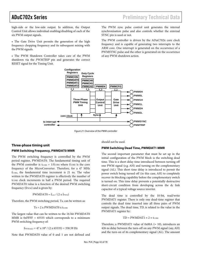
ADuC702x Series Preliminary Technical Data
Rev. PrA | Page 42 of 78
high-side or the low-side output. In addition, the Output Control Unit allows individual enabling/disabling of each of the six PWM output signals.
• The Gate Drive Unit permits the generation of the high frequency chopping frequency and its subsequent mixing with the PWM signals.
• The PWM Shutdown Controller takes care of the PWM shutdown via the PWMTRIP pin and generates the correct RESET signal for the Timing Unit.
The PWM sync pulse control unit generates the internal synchronisation pulse and also controls whether the external SYNC pin is used or not.
The PWM controller is driven by the ADuC702x core clock frequency and is capable of generating two interrupts to the ARM core. One interrupt is generated on the occurrence of a PWMSYNC pulse and the other is generated on the occurrence of any PWM shutdown action.
PWMCONPWMDAT0PWMDAT1PWMDAT2
ConfigurationRegisters
PWMCH0PWMCH1PWMCH2
Duty CycleRegisters
Synccore clock
PWMEN PWMCFG
to interruptcontroller
PWM0H
PWM1H
PWM0L
PWM1LPWM2H
PWM2L
OutputControl
Unit
GateDriveUnit
PWMTRIP
Three-PhasePWM Timing
Unit
PWMSYNC
Figure 21: Overview of the PWM controller
Three-phase timing unit
PWM Switching Frequency, PWMDAT0 MMR
The PWM switching frequency is controlled by the PWM period register, PWMDAT0. The fundamental timing unit of the PWM controller is tCORE = 1/fCORE where fCORE is the core frequency of the MicroConverter. Therefore, for a 47 MHz fCORE, the fundamental time increment is 21 ns. The value written to the PWMDAT0 register is effectively the number of tCORE clock increments in half a PWM period. The required PWMDAT0 value is a function of the desired PWM switching frequency (fPWM) and is given by:
PWMDAT0 = fcore / (2 x fPWM)
Therefore, the PWM switching period, Ts, can be written as:
Ts = 2 x PWMDAT0 x tCORE
The largest value that can be written to the 16-bit PWMDAT0 MMR is 0xFFFF = 65535 which corresponds to a minimum PWM switching frequency of:
fPWM(min) = 47 x 106 / (2 x 65535) = 358.59 Hz
Note that PWMDAT0 value of 0 and 1 are not defined and
should not be used.
PWM Switching Dead Time, PWMDAT1 MMR
The second important parameter that must be set up in the initial configuration of the PWM block is the switching dead time. This is a short delay time introduced between turning off one PWM signal (e.g. AH) and turning on the complementary signal (AL). This short time delay is introduced to permit the power switch being turned off (in this case, AH) to completely recover its blocking capability before the complementary switch is turned on. This time delay prevents a potentially destructive short-circuit condition from developing across the dc link capacitor of a typical voltage source inverter.
The dead time is controlled by the 10-bit, read/write PWMDAT1 register. There is only one dead-time register that controls the dead time inserted into all three pairs of PWM output signals. The dead time, TD, is related to the value in the PWMDAT1 register by:
TD = PWMDAT1 × 2 × tCORE
Therefore, a PWMDAT1 value of 0x00A (= 10), introduces an 426 ns delay between the turn-off on any PWM signal (say, AH) and the turn-on of its complementary signal (AL). The amount
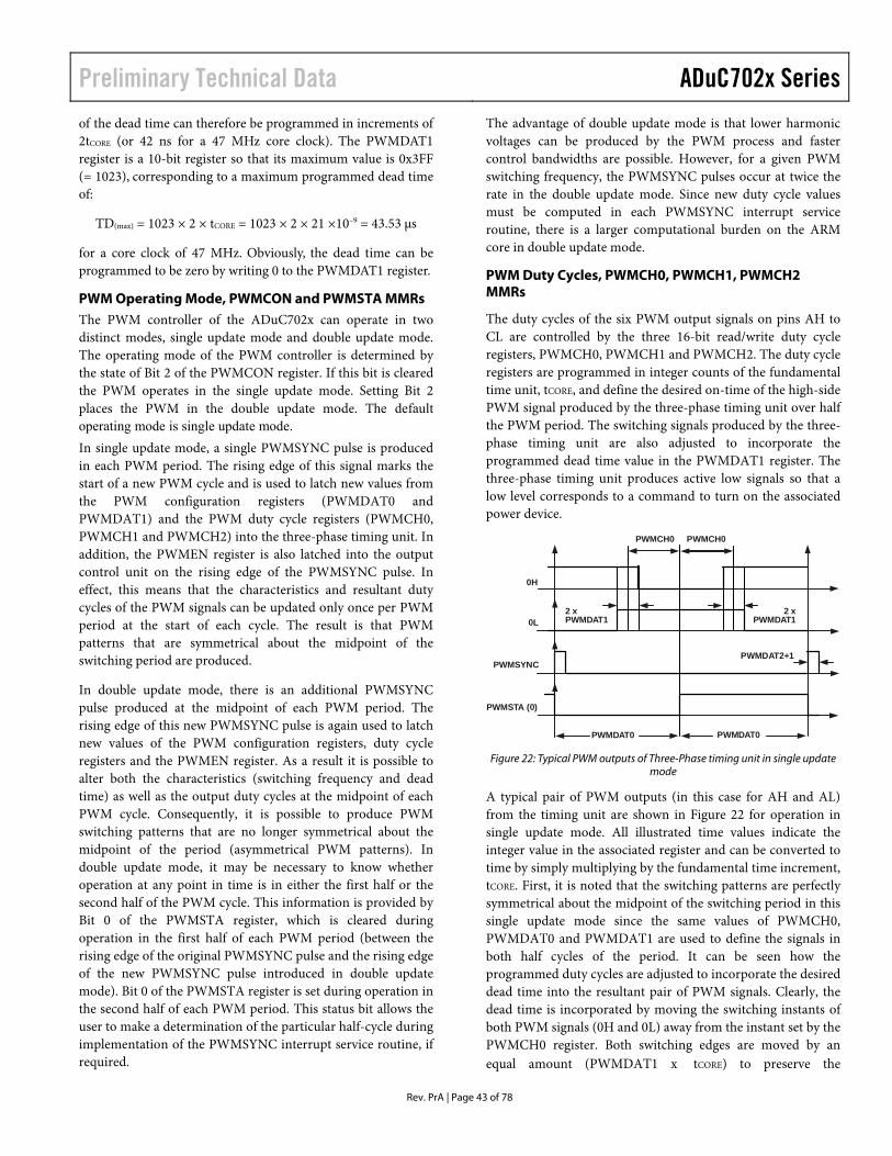
Preliminary Technical Data ADuC702x Series
Rev. PrA | Page 43 of 78
of the dead time can therefore be programmed in increments of 2tCORE (or 42 ns for a 47 MHz core clock). The PWMDAT1 register is a 10-bit register so that its maximum value is 0x3FF (= 1023), corresponding to a maximum programmed dead time of:
TD(max) = 1023 × 2 × tCORE = 1023 × 2 × 21 ×10–9 = 43.53 µs
for a core clock of 47 MHz. Obviously, the dead time can be programmed to be zero by writing 0 to the PWMDAT1 register.
PWM Operating Mode, PWMCON and PWMSTA MMRs The PWM controller of the ADuC702x can operate in two distinct modes, single update mode and double update mode. The operating mode of the PWM controller is determined by the state of Bit 2 of the PWMCON register. If this bit is cleared the PWM operates in the single update mode. Setting Bit 2 places the PWM in the double update mode. The default operating mode is single update mode. In single update mode, a single PWMSYNC pulse is produced in each PWM period. The rising edge of this signal marks the start of a new PWM cycle and is used to latch new values from the PWM configuration registers (PWMDAT0 and PWMDAT1) and the PWM duty cycle registers (PWMCH0, PWMCH1 and PWMCH2) into the three-phase timing unit. In addition, the PWMEN register is also latched into the output control unit on the rising edge of the PWMSYNC pulse. In effect, this means that the characteristics and resultant duty cycles of the PWM signals can be updated only once per PWM period at the start of each cycle. The result is that PWM patterns that are symmetrical about the midpoint of the switching period are produced.
In double update mode, there is an additional PWMSYNC pulse produced at the midpoint of each PWM period. The rising edge of this new PWMSYNC pulse is again used to latch new values of the PWM configuration registers, duty cycle registers and the PWMEN register. As a result it is possible to alter both the characteristics (switching frequency and dead time) as well as the output duty cycles at the midpoint of each PWM cycle. Consequently, it is possible to produce PWM switching patterns that are no longer symmetrical about the midpoint of the period (asymmetrical PWM patterns). In double update mode, it may be necessary to know whether operation at any point in time is in either the first half or the second half of the PWM cycle. This information is provided by Bit 0 of the PWMSTA register, which is cleared during operation in the first half of each PWM period (between the rising edge of the original PWMSYNC pulse and the rising edge of the new PWMSYNC pulse introduced in double update mode). Bit 0 of the PWMSTA register is set during operation in the second half of each PWM period. This status bit allows the user to make a determination of the particular half-cycle during implementation of the PWMSYNC interrupt service routine, if required.
The advantage of double update mode is that lower harmonic voltages can be produced by the PWM process and faster control bandwidths are possible. However, for a given PWM switching frequency, the PWMSYNC pulses occur at twice the rate in the double update mode. Since new duty cycle values must be computed in each PWMSYNC interrupt service routine, there is a larger computational burden on the ARM core in double update mode.
PWM Duty Cycles, PWMCH0, PWMCH1, PWMCH2 MMRs
The duty cycles of the six PWM output signals on pins AH to CL are controlled by the three 16-bit read/write duty cycle registers, PWMCH0, PWMCH1 and PWMCH2. The duty cycle registers are programmed in integer counts of the fundamental time unit, tCORE, and define the desired on-time of the high-side PWM signal produced by the three-phase timing unit over half the PWM period. The switching signals produced by the three-phase timing unit are also adjusted to incorporate the programmed dead time value in the PWMDAT1 register. The three-phase timing unit produces active low signals so that a low level corresponds to a command to turn on the associated power device.
PWMCH0
2 xPWMDAT1
PWMCH0
0H
PWMSTA (0)
0L
PWMDAT0 PWMDAT0
2 xPWMDAT1
PWMSYNCPWMDAT2+1
Figure 22: Typical PWM outputs of Three-Phase timing unit in single update
mode
A typical pair of PWM outputs (in this case for AH and AL) from the timing unit are shown in Figure 22 for operation in single update mode. All illustrated time values indicate the integer value in the associated register and can be converted to time by simply multiplying by the fundamental time increment, tCORE. First, it is noted that the switching patterns are perfectly symmetrical about the midpoint of the switching period in this single update mode since the same values of PWMCH0, PWMDAT0 and PWMDAT1 are used to define the signals in both half cycles of the period. It can be seen how the programmed duty cycles are adjusted to incorporate the desired dead time into the resultant pair of PWM signals. Clearly, the dead time is incorporated by moving the switching instants of both PWM signals (0H and 0L) away from the instant set by the PWMCH0 register. Both switching edges are moved by an equal amount (PWMDAT1 x tCORE) to preserve the
ADuC702x Series Preliminary Technical Data
Rev. PrA | Page 44 of 78
symmetrical output patterns.
Also shown is the PWMSYNC pulse and Bit 0 of the PWMSTA register that indicates whether operation is in the first or second half cycle of the PWM period.
The resultant on-times of the PWM signals over the full PWM period (two half periods) produced by the timing unit can be written as:
T0H = 2 x (PWMCH0 - PWMDAT1) x tCORE
T0L = 2 x (PWMDAT0 – PWMCH0 – PWMDAT1) x tCORE
And the corresponding duty cycles:
d0H = T0H / Ts = (PWMCH0 – PWMDAT1) / PWMDAT0
d0L = T0L / Ts = (PWMDAT0 – PWMCH0 – PWMDAT1) / PWMDAT0
The minimum permissible T0H and T0L values are zero, corresponding to a 0% duty cycle. In a similar fashion, the maximum value is TS, corresponding to a 100% duty cycle.
The output signals from the timing unit for operation in double update mode are shown in Figure 23. This illustrates a completely general case where the switching frequency, dead time and duty cycle are all changed in the second half of the PWM period. Of course, the same value for any or all of these quantities could be used in both halves of the PWM cycle. However, it can be seen that there is no guarantee that symmetrical PWM signals will be produced by the timing unit in double update mode. Additionally, it is seen that the dead time is inserted into the PWM signals in the same way as in the single update mode.
PWMCH01
2 xPWMDAT12
PWMCH02
0H
PWMSTA (0)
0L
PWMDAT01 PWMDAT02
2 xPWMDAT11
PWMSYNCPWMDAT22+1PWMDAT21+1
Figure 23: Typical PWM outputs of the Three-phase timing unit in double
update mode
In general the on-times of the PWM signals in double update mode can be defined as:
T0H = (PWMCH01 + PWMCH02 – PWMDAT11 – PWMDAT12) x tCORE
T0L = (PWMDAT01 + PWMDAT02 - PWMCH01 - PWMCH02 – PWMDAT11 – PWMDAT12) x tCORE
where the subscript 1 refers to the value of that register during the first half cycle and the subscript 2 refers to the value during the second half cycle. The corresponding duty cycles are:
d0H = T0H / Ts = (PWMCH01 + PWMCH02 – PWMDAT11 – PWMDAT12) / (PWMDAT01 + PWMDAT02)
d0L = T0L /Ts = (PWMDAT01 + PWMDAT02 - PWMCH01 - PWMCH02 – PWMDAT11 – PWMDAT12) / (PWMDAT01 + PWMDAT02)
since for the completely general case in double update mode, the switching period is given by:
Ts = (PWMDAT01 + PWMDAT02) x tCORE
Again, the values of T0H and T0L are constrained to lie between zero and TS.
PWM signals similar to those illustrated in Figure 22 and Figure 23 can be produced on the 1H, 1L, 2H and 2L outputs by programming the PWMCH1 and PWMCH2 registers in a manner identical to that described for PWMCH0. The PWM controller does not produce any PWM outputs until all of the PWMDAT0, PWMCH0, PWMCH1 and PWMCH2 registers have been written to at least once. Once these registers have been written, internal counting of the timers in the three-phase timing unit is enabled. Writing to the PWMDAT0 register starts the internal timing of the main PWM timer. Provided the PWMDAT0 register is written prior to the PWMCH0, PWMCH1 and PWMCH2 registers in the initialisation, the first PWMSYNC pulse and interrupt (if enabled) appear 1.5 x tCORE x PWMDAT0 seconds after the initial write to the PWMDAT0 register in single update mode. In double update mode, the first PWMSYNC pulse appears after PWMDAT0 x tCORE seconds.
Output Control Unit
The operation of the Output Control Unit is controlled by the 9-bit read/write PWMEN register. This register controls two distinct features of the Output Control Unit that are directly useful in the control of ECM or BDCM. The PWMEN register contains three crossover bits, one for each pair of PWM outputs. Setting Bit 8 of the PWMEN register enables the crossover mode for the 0H/0L pair of PWM signals, setting Bit 7 enables crossover on the 1H/1L pair of PWM signals and setting Bit 6 enables crossover on the 2H/2L pair of PWM signals. If crossover mode is enabled for any pair of PWM signals, the high-side PWM signal from the timing unit (0H, for example) is diverted to the associated low-side output of the Output Control Unit so that the signal will ultimately appear at the 0L pin. Of course, the corresponding low-side output of the Timing Unit is also diverted to the complementary high-side output of
Preliminary Technical Data ADuC702x Series
Rev. PrA | Page 45 of 78
the Output Control Unit so that the signal appears at the 0H pin. Following a reset, the three crossover bits are cleared so that the crossover mode is disabled on all three pairs of PWM signals. The PWMEN register also contains six bits (Bits 0 to 5) that can be used to individually enable or disable each of the six PWM outputs. If the associated bit of the PWMEN register is set, the corresponding PWM output is disabled irrespective of the value of the corresponding duty cycle register. This PWM output signal will remain in the OFF state as long as the corresponding enable/disable bit of the PWMEN register is set. The implementation of this output enable function is implemented after the crossover function.
Following a reset, all six enable bits of the PWMEN register are cleared so that all PWM outputs are enabled by default. In a manner identical to the duty cycle registers, the PWMEN is latched on the rising edge of the PWMSYNC signal so that changes to this register only become effective at the start of each PWM cycle in single update mode. In double update mode, the PWMEN register can also be updated at the midpoint of the PWM cycle.
In the control of an ECM only two inverter legs are switched at any time and often the high-side device in one leg must be switched ON at the same time as the low-side driver in a second leg. Therefore, by programming identical duty cycles values for two PWM channels (e.g. PWMCH0 = PWMCH1) and setting Bit 7 of the PWMEN register to cross over the 1H/1L pair of PWM signals, it is possible to turn ON the high-side switch of Phase A and the low-side switch of Phase B at the same time. In the control of ECM, it is usual for the third inverter leg (Phase C in this example) to be disabled for a number of PWM cycles. This function is implemented by disabling both the 2H and 2L PWM outputs by setting Bits 0 and 1 of the PWMEN register.
This situation is illustrated in Figure 24, where it can be seen that both the 0H and 1L signals are identical, since PWMCH0 = PWMCH1 and the crossover bit for phase B is set.
2 x PWMDAT12 x PWMDAT1
PWMCH0= PWMCH1
0H
1L
0L
PWMDAT0 PWMDAT0
1H
2L
2H
PWMCH0= PWMCH1
Figure 24. Example active LO PWM signals suitable for ECM control,
PWMCH0 = PWMCH1, crossover BH/BL pair and disable 0L, 1H, 2H and 2L outputs. Operation is in single update mode.
In addition, the other four signals (0L, 1H, 2H and 2L) have been disabled by setting the appropriate enable/disable bits of the PWMEN register. For the situation illustrated in Figure 24, the appropriate value for the PWMEN register is 0x00A7. In normal ECM operation, each inverter leg is disabled for certain periods of time so that the PWMEN register is changed based on the position of the rotor shaft (motor commutation).
Gate Drive Unit
The Gate Drive Unit of the PWM controller adds features that simplify the design of isolated gate drive circuits for PWM inverters. If a transformer-coupled power device gate drive amplifier is used then the active PWM signal must be chopped at a high frequency. The 10-bit read/write PWMCFG register allows the programming of this high frequency chopping mode. The chopped active PWM signals may be required for the high-side drivers only, for the low-side drivers only or for both the high-side and low-side switches. Therefore, independent control of this mode for both high- and low-side switches is included with two separate control bits in the PWMCFG register.
Typical PWM output signals with high frequency chopping enabled on both high-side and low-side signals are shown in Figure 25. Chopping of the high side PWM outputs (0H, 1H and 2H) is enabled by setting Bit 8 of the PWMCFG register. Chopping of the low-side PWM outputs (0L, 1L and 2L) is enabled by setting Bit 9 of the PWMCFG register. The high frequency chopping frequency is controlled by the 8-bit word (GDCLK) placed in Bits 0 to 7 of the PWMCFG register. The period of this high frequency carrier is:
Tchop = (4 x (GDCLK + 1)) x tCORE
and the chopping frequency is therefore an integral subdivision of the MicroConverter core frequency:
fchop = fCORE / (4 x (GDCLK + 1))
The GDCLK value may range from 0 to 255, corresponding to a programmable chopping frequency rate from 45.9 kHz to 11.75 MHz for a 47 MHz core frequency. The gate drive features must be programmed before operation of the PWM controller and typically are not changed during normal operation of the PWM controller. Following a reset, all bits of the PWMCFG register are cleared so that high frequency chopping is disabled, by default.
ADuC702x Series Preliminary Technical Data
Rev. PrA | Page 46 of 78
PWMCH0
2 x PWMDAT12 x PWMDAT1
PWMCH0
0H
0L
PWMDAT0 PWMDAT0
4 x (GDCLK + 1 ) x tCORE
Figure 25: typical PWM signals with high frequency gate chopping enabled
on both high-side and low-side switches
PWM shutdown
In the event of external fault conditions, it is essential that the PWM system be instantaneously shut down in a safe fashion. A low level on the PWMTRIP pin provides an instantaneous, asynchronous (independent of the MicroConverter core clock) shutdown of the PWM controller. All six PWM outputs are placed in the OFF state, i.e. high state. In addition, the PWMSYNC pulse is disabled. The PWMTRIP pin has an internal pull-down resistor so that if the pin becomes disconnected the PWM will be disabled. The state of the PWMTRIP pin can be read from Bit 3 of the PWMSTA register.
On the occurrence of a PWM shutdown command, a PWMTRIP interrupt will be generated, internal timing of the three-phase timing unit of the PWM controller is stopped.
Following a PWM shutdown, the PWM can only be re-enabled (in a PWMTRIP interrupt service routine, for example) by writing to all of the PWMDAT0, PWMCH0, PWMCH1 and PWMCH2 registers. Provided the external fault has been cleared and the PWMTRIP has returned to a high level, internal timing of the three-phase timing unit resumes and new duty-cycle values are latched on the next PWMSYNC boundary.
PWM MMRs interface
The PWM block is controlled via the following nine MMRs:
- PWMCON: control register, enable the PWM, choose the update rate
- PWMSTA: reflects the status of the PWM - PWMDAT0: unsigned 16-bit register for switching period - PWMDAT1: unsigned 10-bit register for dead time - PWMCFG: gate chopping - PWMCH0,CH1,CH2: channel duty cycle for the three
phases - PWMEN: allows enabling channel outputs and crossover. See
bit definition Table 28. - PWMDAT2: unsigned 10-bit register for PWM sync pulse
width.
Table 25: PWMCON MMR Bit Descriptions
Bit Name Description
7-5 Reserved
4 PWM_SYNCSEL External sync select Set to use external sync Cleared to use internal sync
3 PWM_EXTSYNC External sync select Set to select external synchronous sync signal Cleared for asynchronous sync signal
2 PWMDBL Double Update Mode Set to ‘1’ by the user to enable double update mode Clear to ‘0’ by the user to enable single update mode
1 PWM_SYNC_EN PWM synchronisation enable Set by user to enable synchronisation Cleared by user to disable synchronisation
0 PWMEN PWM Enable Bit Set to ‘1’ by the user to enable the PWM Clear to ‘0’ by the user to disable the PWM. Also cleared automatically with PWMTRIP
Table 26: PWMSTA MMR Bit Descriptions
Bit Name Description
15-10 Reserved
9 PWMSYNCINT PWM sync interrupt bit
Preliminary Technical Data ADuC702x Series
Rev. PrA | Page 47 of 78
8 PWMTRIPINT PWM trip interrupt bit
3 PWMTRIP Raw signal from the PWMTRIP pin
2-1 Reserved
0 PWMPHASE PWM Phase Bit Set to ‘1’ by the MicroConverter when the timer is counting down (1st half) Clear to ‘0’ by the MicroConverter when the timer is counting up (2nd half)
Table 27: PWMCFG MMR Bit Descriptions
Bit Name Description
9 CHOPLO low-side Gate Chopping enable bit
8 CHOPHI high-side Gate Chopping enable bit
0:7 GDCLK PWM Gate Chopping Period (unsigned)
Table 28: PWMEN MMR bit descriptions
Bit Name Description
8 0H0L_XOVR Channel 0 Output Crossover Enable Bit Set to ‘1’ by the user to enable channel 0 output crossover Clear to ‘0’ by the user to disable channel 0 output crossover
7 1H1L_XOVR Channel 1 Output Crossover Enable Bit Set to ‘1’ by the user to enable channel 1 output crossover Clear to ‘0’ by the user to disable channel 1 output crossover
6 2H2L_XOVR Channel 2 Output Crossover Enable Bit Set to ‘1’ by the user to enable channel 2 output crossover Clear to ‘0’ by the user to disable channel 2 output crossover
5 0L_EN AL Output Enable Bit Set to ‘1’ by the user to disable the 0L output of the PWM Clear to ‘0’ by the user to enable the 0L output of the PWM
4 0H_EN AH Output Enable Bit Set to ‘1’ by the user to disable the 0H output of the PWM Clear to ‘0’ by the user to enable the 0H output of the PWM
3 1L_EN BL Output Enable Bit Set to ‘1’ by the user to disable the 1L output of the PWM Clear to ‘0’ by the user to enable the 1L output of the PWM
2 1H_EN BH Output Enable Bit Set to ‘1’ by the user to disable the 1H output of the PWM Clear to ‘0’ by the user to enable the 1H output of the PWM
1 2L_EN CL Output Enable Bit Set to ‘1’ by the user to disable the 2L output of the PWM Clear to ‘0’ by the user to enable the 2L output of the PWM
0 2H_EN CH Output Enable Bit Set to ‘1’ by the user to disable the 2H output of the PWM Clear to ‘0’ by the user to enable the 2H output of the PWM
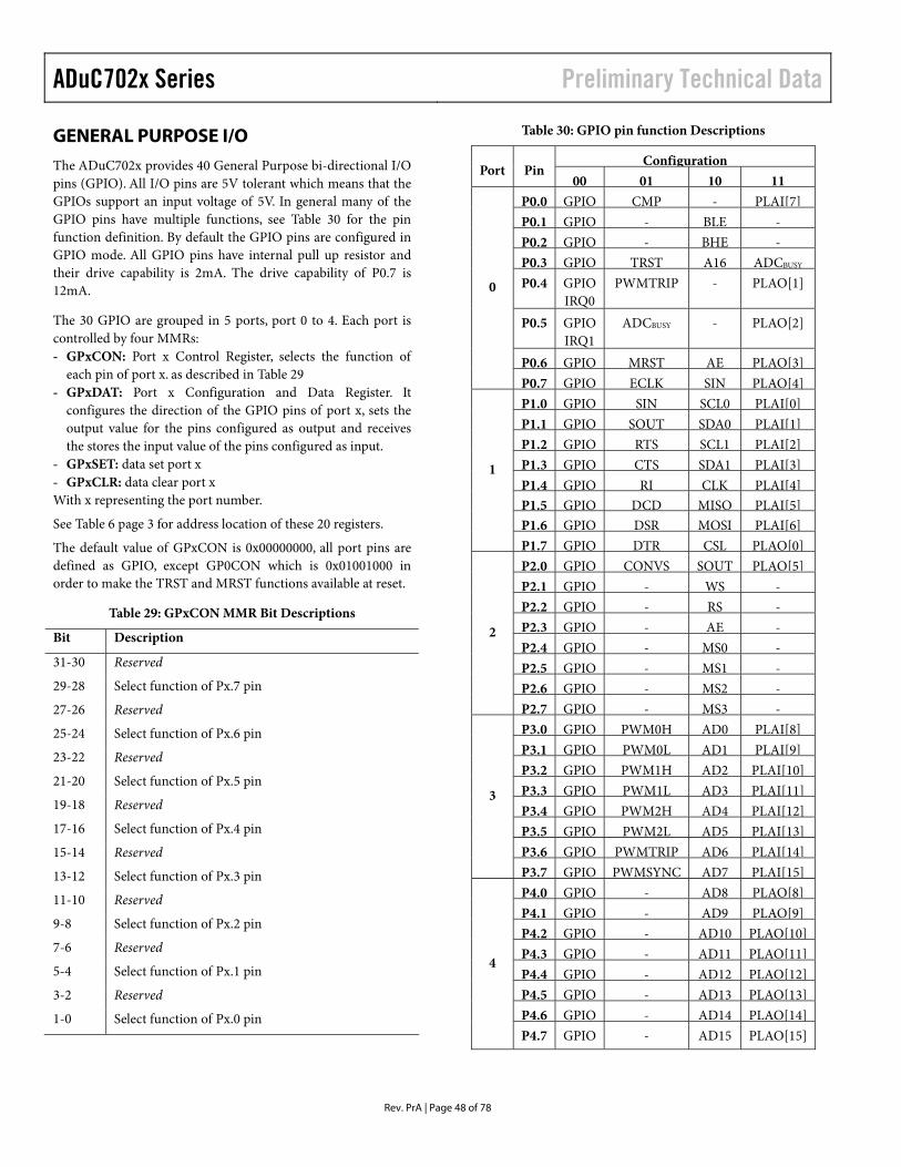
ADuC702x Series Preliminary Technical Data
Rev. PrA | Page 48 of 78
GENERAL PURPOSE I/O
The ADuC702x provides 40 General Purpose bi-directional I/O pins (GPIO). All I/O pins are 5V tolerant which means that the GPIOs support an input voltage of 5V. In general many of the GPIO pins have multiple functions, see Table 30 for the pin function definition. By default the GPIO pins are configured in GPIO mode. All GPIO pins have internal pull up resistor and their drive capability is 2mA. The drive capability of P0.7 is 12mA.
The 30 GPIO are grouped in 5 ports, port 0 to 4. Each port is controlled by four MMRs: - GPxCON: Port x Control Register, selects the function of
each pin of port x. as described in Table 29 - GPxDAT: Port x Configuration and Data Register. It
configures the direction of the GPIO pins of port x, sets the output value for the pins configured as output and receives the stores the input value of the pins configured as input.
- GPxSET: data set port x - GPxCLR: data clear port x With x representing the port number.
See Table 6 page 3 for address location of these 20 registers.
The default value of GPxCON is 0x00000000, all port pins are defined as GPIO, except GP0CON which is 0x01001000 in order to make the TRST and MRST functions available at reset.
Table 29: GPxCON MMR Bit Descriptions
Bit Description
31-30 Reserved
29-28 Select function of Px.7 pin
27-26 Reserved
25-24 Select function of Px.6 pin
23-22 Reserved
21-20 Select function of Px.5 pin
19-18 Reserved
17-16 Select function of Px.4 pin
15-14 Reserved
13-12 Select function of Px.3 pin
11-10 Reserved
9-8 Select function of Px.2 pin
7-6 Reserved
5-4 Select function of Px.1 pin
3-2 Reserved
1-0 Select function of Px.0 pin
Table 30: GPIO pin function Descriptions
ConfigurationPort Pin
00 01 10 11P0.0 GPIO CMP - PLAI[7]P0.1 GPIO - BLE -P0.2 GPIO - BHE -P0.3 GPIO TRST A16 ADCBUSY
P0.4 GPIOIRQ0
PWMTRIP - PLAO[1]
P0.5 GPIOIRQ1
ADCBUSY - PLAO[2]
P0.6 GPIO MRST AE PLAO[3]
0
P0.7 GPIO ECLK SIN PLAO[4]P1.0 GPIO SIN SCL0 PLAI[0]P1.1 GPIO SOUT SDA0 PLAI[1]P1.2 GPIO RTS SCL1 PLAI[2]P1.3 GPIO CTS SDA1 PLAI[3]P1.4 GPIO RI CLK PLAI[4]P1.5 GPIO DCD MISO PLAI[5]P1.6 GPIO DSR MOSI PLAI[6]
1
P1.7 GPIO DTR CSL PLAO[0]P2.0 GPIO CONVS SOUT PLAO[5]P2.1 GPIO - WS -P2.2 GPIO - RS -P2.3 GPIO - AE -P2.4 GPIO - MS0 -P2.5 GPIO - MS1 -P2.6 GPIO - MS2 -
2
P2.7 GPIO - MS3 -P3.0 GPIO PWM0H AD0 PLAI[8]P3.1 GPIO PWM0L AD1 PLAI[9]P3.2 GPIO PWM1H AD2 PLAI[10]P3.3 GPIO PWM1L AD3 PLAI[11]P3.4 GPIO PWM2H AD4 PLAI[12]P3.5 GPIO PWM2L AD5 PLAI[13]P3.6 GPIO PWMTRIP AD6 PLAI[14]
3
P3.7 GPIO PWMSYNC AD7 PLAI[15]P4.0 GPIO - AD8 PLAO[8]P4.1 GPIO - AD9 PLAO[9]P4.2 GPIO - AD10 PLAO[10]P4.3 GPIO - AD11 PLAO[11]P4.4 GPIO - AD12 PLAO[12]P4.5 GPIO - AD13 PLAO[13]P4.6 GPIO - AD14 PLAO[14]
4
P4.7 GPIO - AD15 PLAO[15]
Preliminary Technical Data ADuC702x Series
Rev. PrA | Page 49 of 78
Table 31: GPxDAT MMR Bit Descriptions
Bit Description
31-24 Direction of the data: Set to ‘1’ by the user to configure the GPIO pin as an output Clear to ‘0’ by the user to configure the GPIO pin as an input
23-16 Port x data output
15-8 Reflect the state of Port x pins at reset (read only)
7-0 Port x data input (read only)
Table 32: GPxSET MMR Bit Descriptions
Bit Description
31-24 Reserved
23-16 Data port x set bit: Set to ‘1’ by the user to set bit on port x. will also set the corresponding bit in the GPxDAT MMR Clear to ‘0’ by the user will not affect the data out
15-0 Reserved
Table 33: GPxCLR MMR Bit Descriptions
Bit Description
31-24 Reserved
23-16 Data port x clear bit: Set to ‘1’ by the user to clear bit on port x, will also clear the corresponding bit in the GPxDAT MMR Clear to ‘0’ by the user will not affect the data out
15-0 Reserved
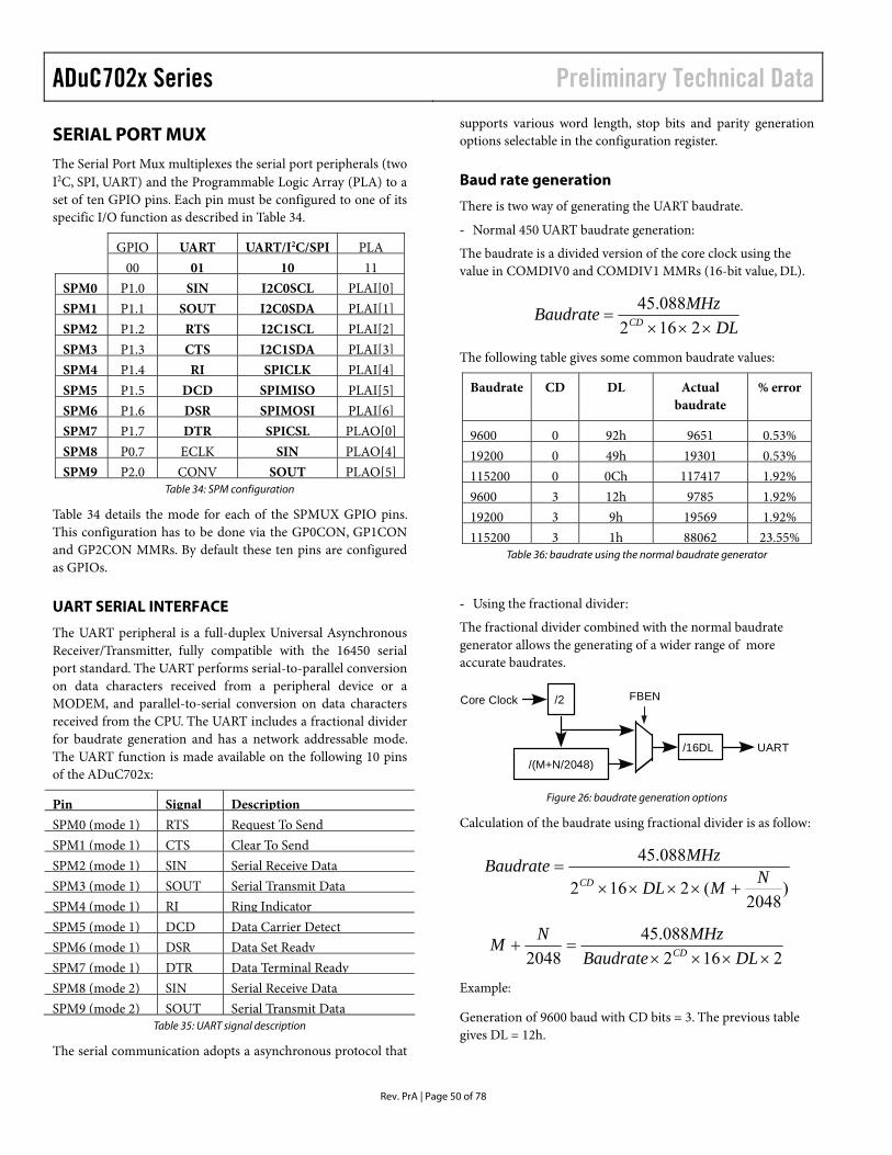
ADuC702x Series Preliminary Technical Data
Rev. PrA | Page 50 of 78
SERIAL PORT MUX
The Serial Port Mux multiplexes the serial port peripherals (two I2C, SPI, UART) and the Programmable Logic Array (PLA) to a set of ten GPIO pins. Each pin must be configured to one of its specific I/O function as described in Table 34.
GPIO UART UART/I2C/SPI PLA
00 01 10 11SPM0 P1.0 SIN I2C0SCL PLAI[0]SPM1 P1.1 SOUT I2C0SDA PLAI[1]SPM2 P1.2 RTS I2C1SCL PLAI[2]SPM3 P1.3 CTS I2C1SDA PLAI[3]SPM4 P1.4 RI SPICLK PLAI[4]SPM5 P1.5 DCD SPIMISO PLAI[5]SPM6 P1.6 DSR SPIMOSI PLAI[6]SPM7 P1.7 DTR SPICSL PLAO[0]SPM8 P0.7 ECLK SIN PLAO[4]SPM9 P2.0 CONV SOUT PLAO[5]
Table 34: SPM configuration
Table 34 details the mode for each of the SPMUX GPIO pins. This configuration has to be done via the GP0CON, GP1CON and GP2CON MMRs. By default these ten pins are configured as GPIOs.
UART SERIAL INTERFACE
The UART peripheral is a full-duplex Universal Asynchronous Receiver/Transmitter, fully compatible with the 16450 serial port standard. The UART performs serial-to-parallel conversion on data characters received from a peripheral device or a MODEM, and parallel-to-serial conversion on data characters received from the CPU. The UART includes a fractional divider for baudrate generation and has a network addressable mode. The UART function is made available on the following 10 pins of the ADuC702x:
Pin Signal Description SPM0 (mode 1) RTS Request To Send SPM1 (mode 1) CTS Clear To Send SPM2 (mode 1) SIN Serial Receive Data SPM3 (mode 1) SOUT Serial Transmit Data SPM4 (mode 1) RI Ring Indicator SPM5 (mode 1) DCD Data Carrier Detect SPM6 (mode 1) DSR Data Set Ready SPM7 (mode 1) DTR Data Terminal Ready SPM8 (mode 2) SIN Serial Receive Data SPM9 (mode 2) SOUT Serial Transmit Data
Table 35: UART signal description
The serial communication adopts a asynchronous protocol that
supports various word length, stop bits and parity generation options selectable in the configuration register.
Baud rate generation
There is two way of generating the UART baudrate.
- Normal 450 UART baudrate generation:
The baudrate is a divided version of the core clock using the value in COMDIV0 and COMDIV1 MMRs (16-bit value, DL).
DLMHzBaudrate CD ×××
=2162
088.45
The following table gives some common baudrate values:
Baudrate CD DL Actual baudrate
% error
9600 0 92h 9651 0.53%19200 0 49h 19301 0.53%115200 0 0Ch 117417 1.92%9600 3 12h 9785 1.92%19200 3 9h 19569 1.92%115200 3 1h 88062 23.55%
Table 36: baudrate using the normal baudrate generator
- Using the fractional divider:
The fractional divider combined with the normal baudrate generator allows the generating of a wider range of more accurate baudrates.
Core Clock
/(M+N/2048)/16DL UART
FBEN/2
Figure 26: baudrate generation options
Calculation of the baudrate using fractional divider is as follow:
)2048
(2162
088.45NMDL
MHzBaudrateCD +××××
=
2162088.45
2048 ××××=+
DLBaudrateMHzNM CD
Example:
Generation of 9600 baud with CD bits = 3. The previous table gives DL = 12h.
Preliminary Technical Data ADuC702x Series
Rev. PrA | Page 51 of 78
2181629600088.45
2048 3 ××××=+
MHzNM
019.12048
=+NM
M = 1 and N = 0.019 x 2048 = 39
)2048391(218162
088.453 +××××
=MHzBaudrate
Baudrate = 9602 bps
Error = 0.02% compared to 1.92% with the normal baudrate generator.
UART registers definition
The UART interface consists on 12 registers namely:
- COMTX: 8-bit transmit register - COMRX: 8-bit receive register - COMDIV0: divisor latch (low byte)
COMTX, COMRX and COMDIV0 share the same address location. COMTX and COMTX can be accessed when bit 7 in COMCON0 register is cleared. COMDIV0 can be accessed when bit 7 of COMCON0 is set.
- COMDIV1: divisor latch (high byte) - COMCON0: line control register - COMSTA0: line status register - COMIEN0: interrupt enable register - COMIID0: interrupt identification register - COMCON1: modem control register - COMSTA1: modem status register - COMDIV2: 16-bit fractional baud divide register - COMSCR: 8-bit scratch register used for temporary storage.
Also used in network addressable UART mode.
Table 37: COMCON0 MMR Bit Descriptions
Bit Name Description
7 DLAB Divisor latch access Set by user to enable access to COMDIV0 and COMDIV1 registers Cleared by user to disable access to COMDIV0 and COMDIV1 and enable access to COMRX and COMTX
6 BRK Set break. Set by user to force SOUT to 0 Cleared to operate in normal mode
5 SP Stick parity Set by user to force parity to defined values: 1 if EPS = 1 and PEN = 1 0 if EPS = 0 and PEN = 1
4 EPS Even parity select bit Set for even parity Cleared for odd parity
3 PEN Parity enable bit: Set by user to transmit and check the parity bit Cleared by user for no parity transmission or checking
2 STOP Stop bit Set by user to transmit 1.5 Stop bit if the Word Length is 5 bits or 2 Stop bits if the word length is 6, 7 or 8 bits. The receiver checks the first Stop bit only, regardless of the number of Stop bits selected Cleared by user to generate 1 Stop bit in the transmitted data
1-0 WLS Word length select: 00 = 5 bits 01 = 6 bits 10 = 7 bits 11 = 8 bits
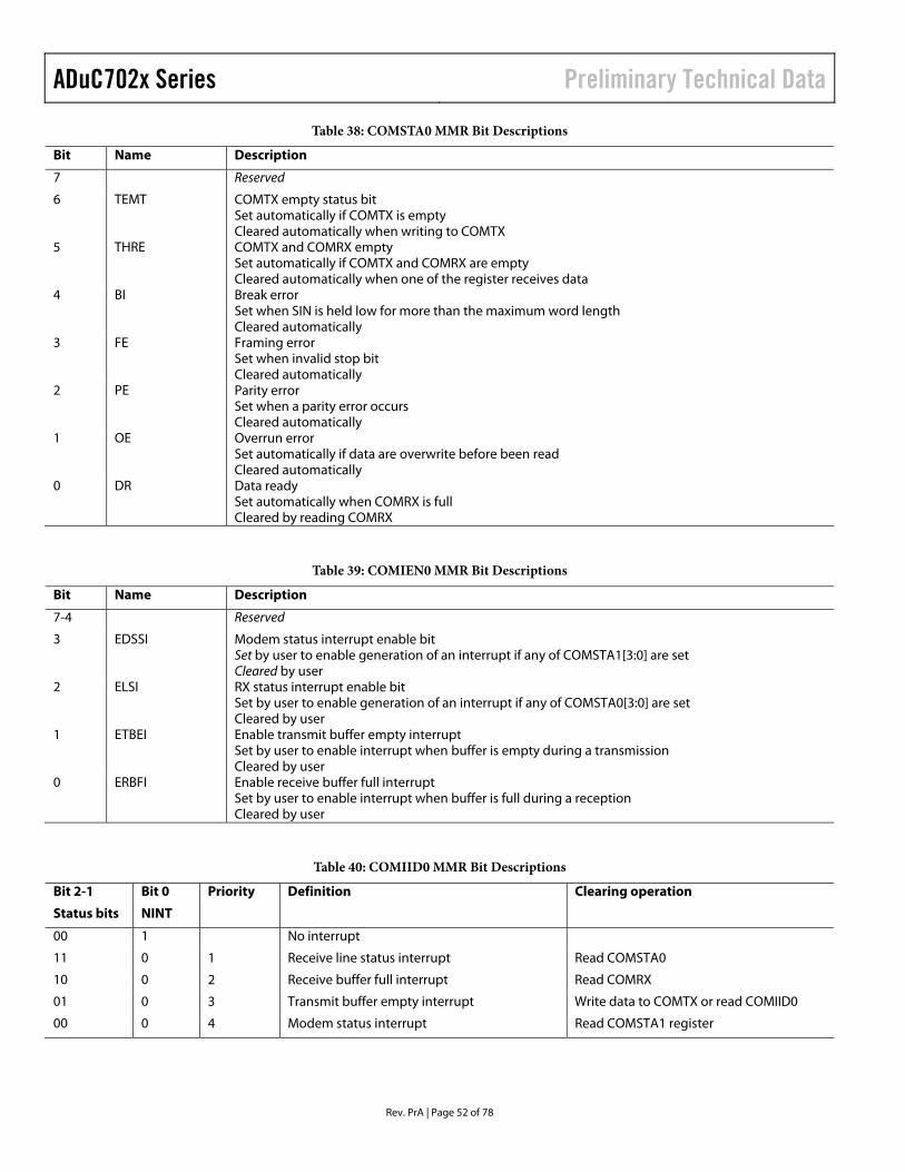
ADuC702x Series Preliminary Technical Data
Rev. PrA | Page 52 of 78
Table 38: COMSTA0 MMR Bit Descriptions
Bit Name Description
7 Reserved
6 TEMT COMTX empty status bit Set automatically if COMTX is empty Cleared automatically when writing to COMTX
5 THRE COMTX and COMRX empty Set automatically if COMTX and COMRX are empty Cleared automatically when one of the register receives data
4 BI Break error Set when SIN is held low for more than the maximum word length Cleared automatically
3 FE Framing error Set when invalid stop bit Cleared automatically
2 PE Parity error Set when a parity error occurs Cleared automatically
1 OE Overrun error Set automatically if data are overwrite before been read Cleared automatically
0 DR Data ready Set automatically when COMRX is full Cleared by reading COMRX
Table 39: COMIEN0 MMR Bit Descriptions
Bit Name Description
7-4 Reserved
3 EDSSI Modem status interrupt enable bit Set by user to enable generation of an interrupt if any of COMSTA1[3:0] are set Cleared by user
2 ELSI RX status interrupt enable bit Set by user to enable generation of an interrupt if any of COMSTA0[3:0] are set Cleared by user
1 ETBEI Enable transmit buffer empty interrupt Set by user to enable interrupt when buffer is empty during a transmission Cleared by user
0 ERBFI Enable receive buffer full interrupt Set by user to enable interrupt when buffer is full during a reception Cleared by user
Table 40: COMIID0 MMR Bit Descriptions
Bit 2-1
Status bits
Bit 0
NINT
Priority Definition Clearing operation
00 1 No interrupt
11 0 1 Receive line status interrupt Read COMSTA0
10 0 2 Receive buffer full interrupt Read COMRX
01 0 3 Transmit buffer empty interrupt Write data to COMTX or read COMIID0
00 0 4 Modem status interrupt Read COMSTA1 register
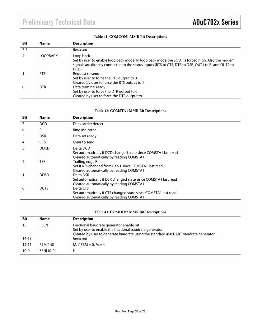
Preliminary Technical Data ADuC702x Series
Rev. PrA | Page 53 of 78
Table 41: COMCON1 MMR Bit Descriptions
Bit Name Description
7-5 Reserved
4 LOOPBACK Loop back Set by user to enable loop back mode. In loop back mode the SOUT is forced high. Also the modem signals are directly connected to the status inputs (RTS to CTS, DTR to DSR, OUT1 to RI and OUT2 to DCD)
1 RTS Request to send Set by user to force the RTS output to 0 Cleared by user to force the RTS output to 1
0 DTR Data terminal ready Set by user to force the DTR output to 0 Cleared by user to force the DTR output to 1
Table 42: COMSTA1 MMR Bit Descriptions
Bit Name Description
7 DCD Data carrier detect
6 RI Ring indicator
5 DSR Data set ready
4 CTS Clear to send
3 DDCD Delta DCD Set automatically if DCD changed state since COMSTA1 last read Cleared automatically by reading COMSTA1
2 TERI Trailing edge RI Set if NRI changed from 0 to 1 since COMSTA1 last read Cleared automatically by reading COMSTA1
1 DDSR Delta DSR Set automatically if DSR changed state since COMSTA1 last read Cleared automatically by reading COMSTA1
0 DCTS Delta CTS Set automatically if CTS changed state since COMSTA1 last read Cleared automatically by reading COMSTA1
Table 43: COMDIV2 MMR Bit Descriptions
Bit Name Description
15 FBEN Fractional baudrate generator enable bit Set by user to enable the fractional baudrate generator Cleared by user to generate baudrate using the standard 450 UART baudrate generator
14-13 Reserved
12-11 FBM[1-0] M. if FBM = 0, M = 4
10-0 FBN[10-0] N
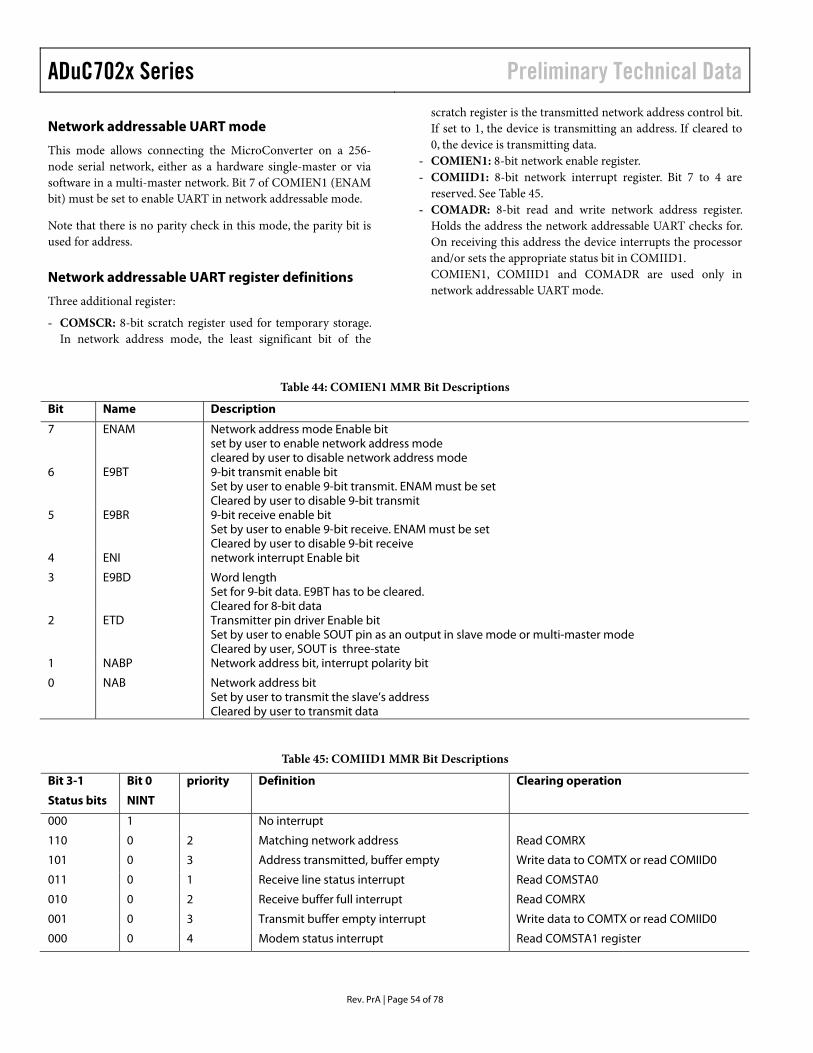
ADuC702x Series Preliminary Technical Data
Rev. PrA | Page 54 of 78
Network addressable UART mode
This mode allows connecting the MicroConverter on a 256-node serial network, either as a hardware single-master or via software in a multi-master network. Bit 7 of COMIEN1 (ENAM bit) must be set to enable UART in network addressable mode.
Note that there is no parity check in this mode, the parity bit is used for address.
Network addressable UART register definitions
Three additional register:
- COMSCR: 8-bit scratch register used for temporary storage. In network address mode, the least significant bit of the
scratch register is the transmitted network address control bit. If set to 1, the device is transmitting an address. If cleared to 0, the device is transmitting data.
- COMIEN1: 8-bit network enable register. - COMIID1: 8-bit network interrupt register. Bit 7 to 4 are
reserved. See Table 45. - COMADR: 8-bit read and write network address register.
Holds the address the network addressable UART checks for. On receiving this address the device interrupts the processor and/or sets the appropriate status bit in COMIID1. COMIEN1, COMIID1 and COMADR are used only in network addressable UART mode.
Table 44: COMIEN1 MMR Bit Descriptions
Bit Name Description
7 ENAM Network address mode Enable bit set by user to enable network address mode cleared by user to disable network address mode
6 E9BT 9-bit transmit enable bit Set by user to enable 9-bit transmit. ENAM must be set Cleared by user to disable 9-bit transmit
5 E9BR 9-bit receive enable bit Set by user to enable 9-bit receive. ENAM must be set Cleared by user to disable 9-bit receive
4 ENI network interrupt Enable bit
3 E9BD Word length Set for 9-bit data. E9BT has to be cleared. Cleared for 8-bit data
2 ETD Transmitter pin driver Enable bit Set by user to enable SOUT pin as an output in slave mode or multi-master mode Cleared by user, SOUT is three-state
1 NABP Network address bit, interrupt polarity bit
0 NAB Network address bit Set by user to transmit the slave’s address Cleared by user to transmit data
Table 45: COMIID1 MMR Bit Descriptions
Bit 3-1
Status bits
Bit 0
NINT
priority Definition Clearing operation
000 1 No interrupt
110 0 2 Matching network address Read COMRX
101 0 3 Address transmitted, buffer empty Write data to COMTX or read COMIID0
011 0 1 Receive line status interrupt Read COMSTA0
010 0 2 Receive buffer full interrupt Read COMRX
001 0 3 Transmit buffer empty interrupt Write data to COMTX or read COMIID0
000 0 4 Modem status interrupt Read COMSTA1 register
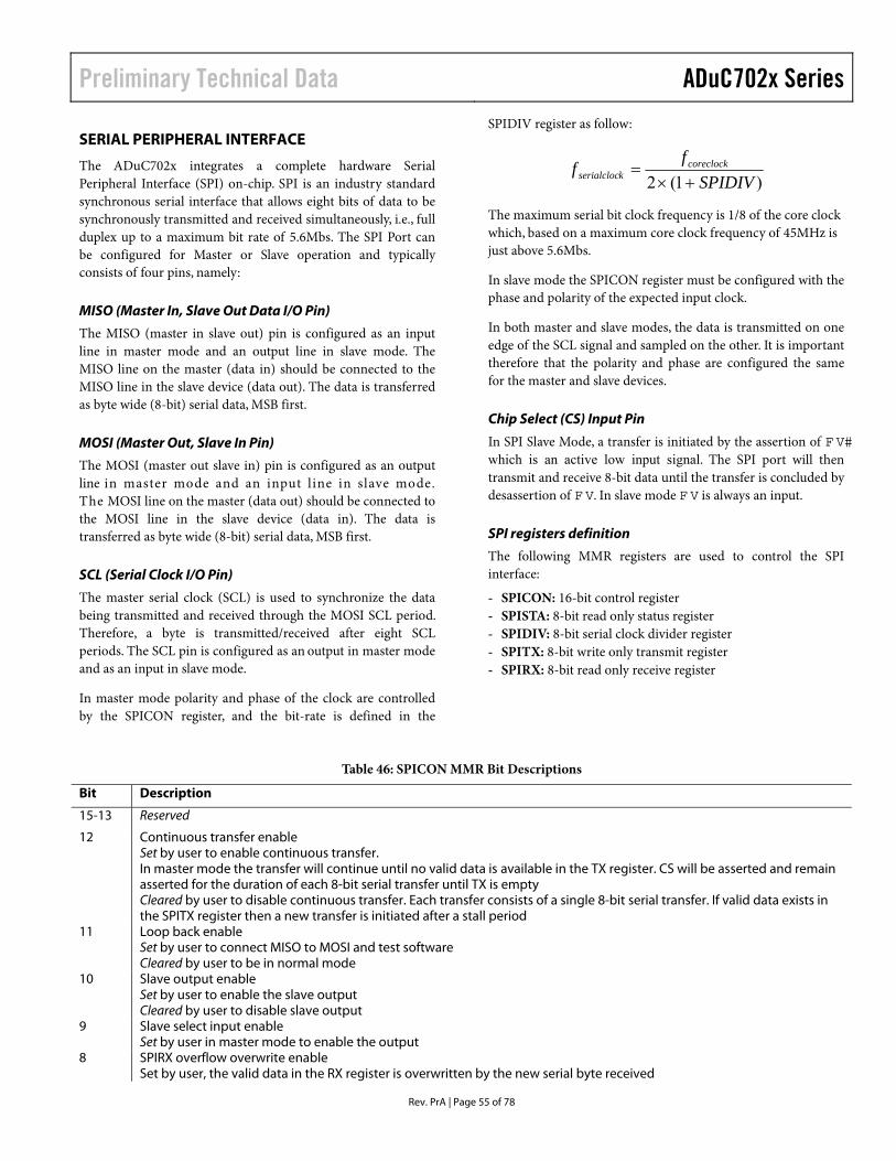
Preliminary Technical Data ADuC702x Series
Rev. PrA | Page 55 of 78
SERIAL PERIPHERAL INTERFACE
The ADuC702x integrates a complete hardware Serial Peripheral Interface (SPI) on-chip. SPI is an industry standard synchronous serial interface that allows eight bits of data to be synchronously transmitted and received simultaneously, i.e., full duplex up to a maximum bit rate of 5.6Mbs. The SPI Port can be configured for Master or Slave operation and typically consists of four pins, namely:
MISO (Master In, Slave Out Data I/O Pin)
The MISO (master in slave out) pin is configured as an input line in master mode and an output line in slave mode. The MISO line on the master (data in) should be connected to the MISO line in the slave device (data out). The data is transferred as byte wide (8-bit) serial data, MSB first.
MOSI (Master Out, Slave In Pin)
The MOSI (master out slave in) pin is configured as an output line in master mode and an input line in slave mode. The MOSI line on the master (data out) should be connected to the MOSI line in the slave device (data in). The data is transferred as byte wide (8-bit) serial data, MSB first.
SCL (Serial Clock I/O Pin)
The master serial clock (SCL) is used to synchronize the data being transmitted and received through the MOSI SCL period. Therefore, a byte is transmitted/received after eight SCL periods. The SCL pin is configured as an output in master mode and as an input in slave mode.
In master mode polarity and phase of the clock are controlled by the SPICON register, and the bit-rate is defined in the
SPIDIV register as follow:
)1(2 SPIDIVf
f coreclockkserialcloc +×
=
The maximum serial bit clock frequency is 1/8 of the core clock which, based on a maximum core clock frequency of 45MHz is just above 5.6Mbs.
In slave mode the SPICON register must be configured with the phase and polarity of the expected input clock.
In both master and slave modes, the data is transmitted on one edge of the SCL signal and sampled on the other. It is important therefore that the polarity and phase are configured the same for the master and slave devices.
Chip Select (CS) Input Pin
In SPI Slave Mode, a transfer is initiated by the assertion of C S which is an active low input signal. The SPI port will then transmit and receive 8-bit data until the transfer is concluded by desassertion of CS. In slave mode CS is always an input.
SPI registers definition
The following MMR registers are used to control the SPI interface:
- SPICON: 16-bit control register - SPISTA: 8-bit read only status register - SPIDIV: 8-bit serial clock divider register - SPITX: 8-bit write only transmit register - SPIRX: 8-bit read only receive register
Table 46: SPICON MMR Bit Descriptions
Bit Description
15-13 Reserved
12 Continuous transfer enable Set by user to enable continuous transfer. In master mode the transfer will continue until no valid data is available in the TX register. CS will be asserted and remain asserted for the duration of each 8-bit serial transfer until TX is empty Cleared by user to disable continuous transfer. Each transfer consists of a single 8-bit serial transfer. If valid data exists in the SPITX register then a new transfer is initiated after a stall period
11 Loop back enable Set by user to connect MISO to MOSI and test software Cleared by user to be in normal mode
10 Slave output enable Set by user to enable the slave output Cleared by user to disable slave output
9 Slave select input enable Set by user in master mode to enable the output
8 SPIRX overflow overwrite enable Set by user, the valid data in the RX register is overwritten by the new serial byte received
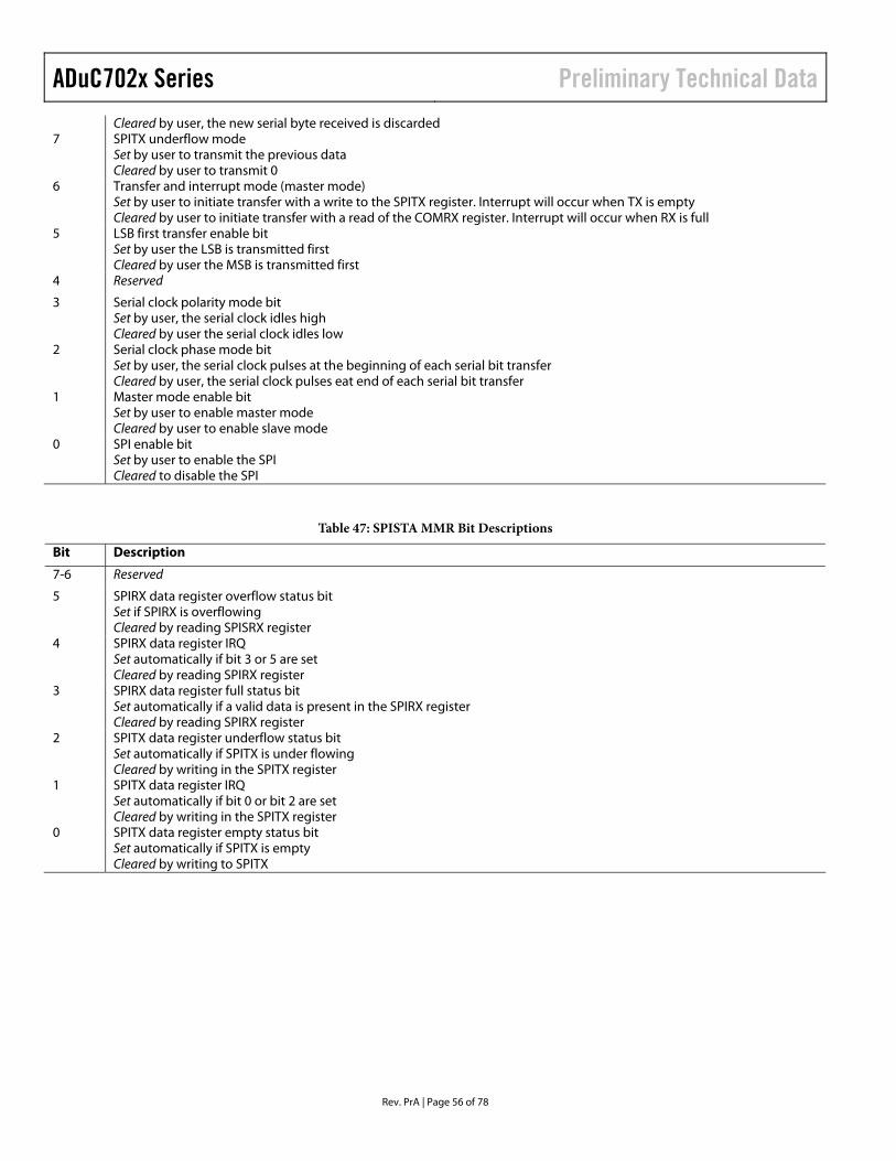
ADuC702x Series Preliminary Technical Data
Rev. PrA | Page 56 of 78
Cleared by user, the new serial byte received is discarded 7 SPITX underflow mode
Set by user to transmit the previous data Cleared by user to transmit 0
6 Transfer and interrupt mode (master mode) Set by user to initiate transfer with a write to the SPITX register. Interrupt will occur when TX is empty Cleared by user to initiate transfer with a read of the COMRX register. Interrupt will occur when RX is full
5 LSB first transfer enable bit Set by user the LSB is transmitted first Cleared by user the MSB is transmitted first
4 Reserved
3 Serial clock polarity mode bit Set by user, the serial clock idles high Cleared by user the serial clock idles low
2 Serial clock phase mode bit Set by user, the serial clock pulses at the beginning of each serial bit transfer Cleared by user, the serial clock pulses eat end of each serial bit transfer
1 Master mode enable bit Set by user to enable master mode Cleared by user to enable slave mode
0 SPI enable bit Set by user to enable the SPI Cleared to disable the SPI
Table 47: SPISTA MMR Bit Descriptions
Bit Description
7-6 Reserved
5 SPIRX data register overflow status bit Set if SPIRX is overflowing Cleared by reading SPISRX register
4 SPIRX data register IRQ Set automatically if bit 3 or 5 are set Cleared by reading SPIRX register
3 SPIRX data register full status bit Set automatically if a valid data is present in the SPIRX register Cleared by reading SPIRX register
2 SPITX data register underflow status bit Set automatically if SPITX is under flowing Cleared by writing in the SPITX register
1 SPITX data register IRQ Set automatically if bit 0 or bit 2 are set Cleared by writing in the SPITX register
0 SPITX data register empty status bit Set automatically if SPITX is empty Cleared by writing to SPITX
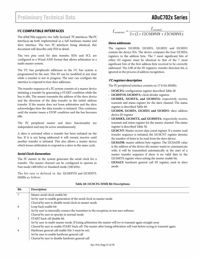
Preliminary Technical Data ADuC702x Series
Rev. PrA | Page 57 of 78
I2C COMPATIBLE INTERFACES
The ADuC702x supports two fully licensed* I2C interfaces. The I2C interfaces are both implemented as a full hardware master and slave interface. The two I2C interfaces being identical, this document will describe only I2C0 in detail.
The two pins used for data transfer, SDA and SCL are configured in a Wired-AND format that allows arbitration in a multi-master system.
The I2C bus peripheral’s addresses in the I2C bus system is programmed by the user. This ID can be modified at any time while a transfer is not in progress. The user can configure the interface to respond to four slave addresses.
The transfer sequence of a I2C system consists of a master device initiating a transfer by generating a START condition while the bus is idle. The master transmits the address of the slave device and the direction of the data transfer in the initial address transfer. If the master does not loose arbitration and the slave acknowledges then the data transfer is initiated. This continues until the master issues a STOP condition and the bus becomes idle.
The I2C peripheral master and slave functionality are independent and may be active simultaneously.
A slave is activated when a transfer has been initiated on the bus. If it is not being addressed it will remain inactive until another transfer is initiated. This also allows a master device which looses arbitration to respond as a slave in the same cycle.
Serial Clock Generation
The I2C master in the system generates the serial clock for a transfer. The master channel can be configured to operate in Fast mode (400 kHz) or Standard mode (100 kHz).
The bit-rate is def ined in the I2C0DIVH and I2C0DIVL MMRs as follow:
)02022(2 DIVLCIDIVHCIf
f coreclockkserialcloc ++×
=
Slave addresses
The registers I2C0ID0, I2C0ID1, I2C0ID2 and I2C0ID3 contain the device IDs. The device compares the four I2C0IDx registers to the address byte. The 7 most significant bits of either ID register must be identical to that of the 7 most significant bits of the first address byte received to be correctly addressed. The LSB of the ID registers, transfer direction bit, is ignored in the process of address recognition.
I2C registers description
The I2C peripheral interface consists on 17 8-bit MMRs:
- I2C0CFG: configuration register described Table 48 - I2C0DIVH, I2C0DIVL: clock divider registers - I2C0SRX, I2C0STX, and I2C0SSTA: respectively receive,
transmit and status register for the slave channel. The status register is described Table 49.
- I2C0ID0, I2C0ID1, I2C0ID2 and I2C0ID3: slave address device ID register
- I2C0MRX, I2C0MTX, and I2C0MSTA: respectively receive, transmit and status register for the master channel. The status register is described Table 50.
- I2C0CNT: Master receive data count register. If a master read transfer sequence is initiated, the I2C0CNT register denotes the number of bytes to be read from the slave device.
- I2C0ADR: master address byte register. The I2C0ADR value is the address of the device the master wants to communicate with, it will be transmitted automatically at the start of a master transfer sequence if there is no valid data in the I2C0MTX register when setting the master enable bit.
- I2C0ALT: hardware general call ID register, used in slave mode
Table 48: I2C0CFG MMR Bit Descriptions
Bit Description
7 Master serial clock enable bit Set by user to enable generation of the serial clock in master mode Cleared by user to disable serial clock in master mode
6 Loop back enable bit Set by user to internally connect the transition to the reception, to test user software Cleared by user to operate in normal mode
5 START back-off disable bit Set by user in multi-master mode. If losing arbitration the master will try to transmit again straight away Cleared by user to enable START back-off. The master after losing arbitration will wait before trying to transmit again
4 Hardware general call enable (bit 3 must be set) Set by user to enable hardware general call Cleared by user to disable hardware general call
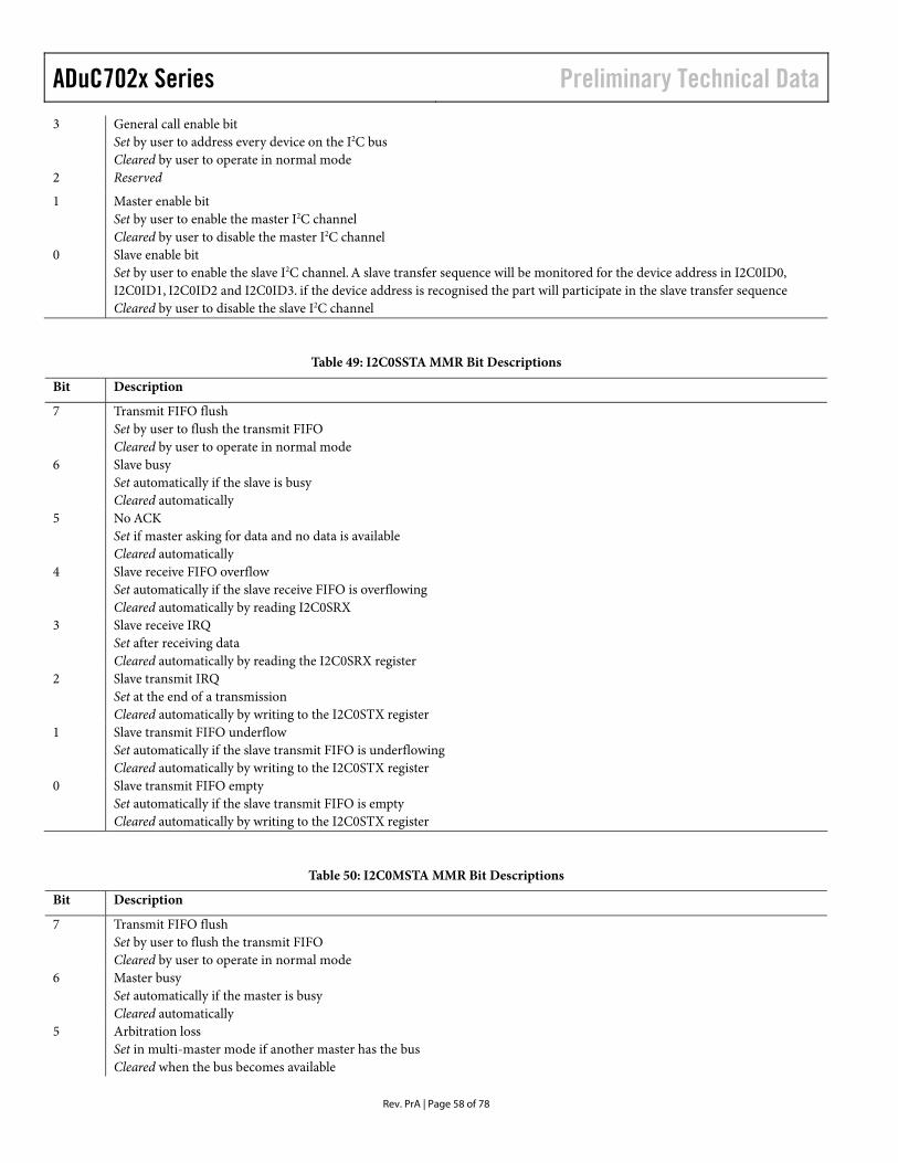
ADuC702x Series Preliminary Technical Data
Rev. PrA | Page 58 of 78
3 General call enable bit Set by user to address every device on the I2C bus Cleared by user to operate in normal mode
2 Reserved
1 Master enable bit Set by user to enable the master I2C channel Cleared by user to disable the master I2C channel
0 Slave enable bit Set by user to enable the slave I2C channel. A slave transfer sequence will be monitored for the device address in I2C0ID0, I2C0ID1, I2C0ID2 and I2C0ID3. if the device address is recognised the part will participate in the slave transfer sequence Cleared by user to disable the slave I2C channel
Table 49: I2C0SSTA MMR Bit Descriptions
Bit Description
7 Transmit FIFO flush Set by user to flush the transmit FIFO Cleared by user to operate in normal mode
6 Slave busy Set automatically if the slave is busy Cleared automatically
5 No ACK Set if master asking for data and no data is available Cleared automatically
4 Slave receive FIFO overflow Set automatically if the slave receive FIFO is overflowing Cleared automatically by reading I2C0SRX
3 Slave receive IRQ Set after receiving data Cleared automatically by reading the I2C0SRX register
2 Slave transmit IRQ Set at the end of a transmission Cleared automatically by writing to the I2C0STX register
1 Slave transmit FIFO underflow Set automatically if the slave transmit FIFO is underflowing Cleared automatically by writing to the I2C0STX register
0 Slave transmit FIFO empty Set automatically if the slave transmit FIFO is empty Cleared automatically by writing to the I2C0STX register
Table 50: I2C0MSTA MMR Bit Descriptions
Bit Description
7 Transmit FIFO flush Set by user to flush the transmit FIFO Cleared by user to operate in normal mode
6 Master busy Set automatically if the master is busy Cleared automatically
5 Arbitration loss Set in multi-master mode if another master has the bus Cleared when the bus becomes available
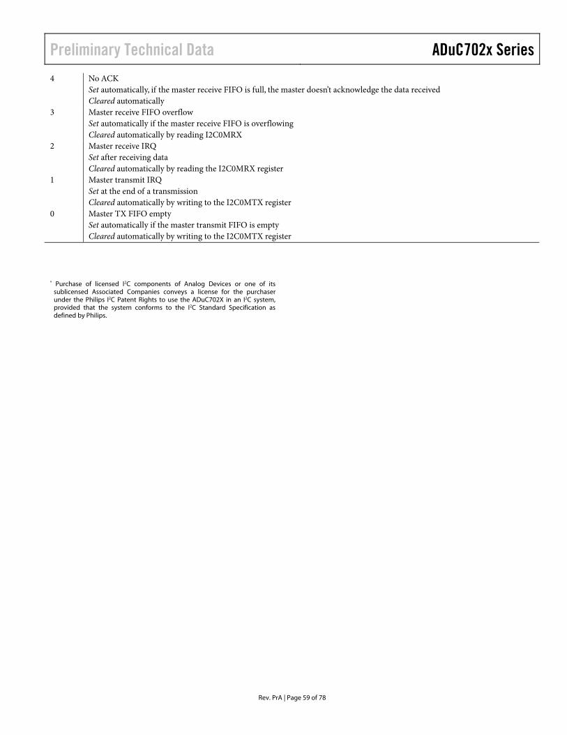
Preliminary Technical Data ADuC702x Series
Rev. PrA | Page 59 of 78
4 No ACK Set automatically, if the master receive FIFO is full, the master doesn’t acknowledge the data received Cleared automatically
3 Master receive FIFO overflow Set automatically if the master receive FIFO is overflowing Cleared automatically by reading I2C0MRX
2 Master receive IRQ Set after receiving data Cleared automatically by reading the I2C0MRX register
1 Master transmit IRQ Set at the end of a transmission Cleared automatically by writing to the I2C0MTX register
0 Master TX FIFO empty Set automatically if the master transmit FIFO is empty Cleared automatically by writing to the I2C0MTX register
* Purchase of licensed I2C components of Analog Devices or one of its
sublicensed Associated Companies conveys a license for the purchaser under the Philips I2C Patent Rights to use the ADuC702X in an I2C system, provided that the system conforms to the I2C Standard Specification as defined by Philips.
ADuC702x Series Preliminary Technical Data
Rev. PrA | Page 60 of 78
PROGRAMMABLE LOGIC ARRAY (PLA)
The ADuC702x integrates a fully Programmable Logic Array (PLA) which consists of two independent but interconnected PLA blocks. Each block consists of eight PLA elements, which gives a total of 16 PLA elements.
A PLA element contains a two-input lookup table that can be configured to generate any logic output function based on two inputs and a flip-flop as represented in Figure 27 below.
0
1
2
3
4LOOK-UP
TABLE
A
B
Figure 27: PLA element
In total, 30 GPIO pins are available on the ADuC702x for the PLA. These include 16 input pins and 14 output pins. They need to be configured in the GPxCON register as PLA pins before using the PLA. Note that the comparator output is also included as one of the 16 input pins.
The PLA is configured via a set of user MMRs and the output(s) of the PLA can be routed to the internal interrupt system, to the CONVSTART signal of the ADC, to a MMR or to any of the 16 PLA output pins.
The interconnection between the two block is supported by connecting output of element 7 of block 1 fed back to the input 0 of mux 0 of element 0 of block 0, and the output of element 7 of block 0 is fed back to the input 0 of mux 0 of element 0 of block 1.
PLA Block 0 PLA Block 1
Element Input Output Element Input Output
0 P1.0 P1.7 8 P3.0 P4.0
1 P1.1 P0.4 9 P3.1 P4.1
2 P1.2 P0.5 10 P3.2 P4.2
3 P1.3 P0.6 11 P3.3 P4.3
4 P1.4 P0.7 12 P3.4 P4.4
5 P1.5 P2.0 13 P3.5 P4.5
6 P1.6 - 14 P3.6 P4.6
7 P0.0 - 15 P3.7 P4.7
Table 51: element input/output
PLA MMRs interface
The PLA peripheral interface consists on 21 MMRs:
- PLAELMx: element0 to element 15 control registers, configure the input and output mux of each element, select the function in the lookup table and enable/disable the flip-flop.
- PLACLK: clock selection for the flip-flops of block 0 and clock selection for the flip-flops of block 1
- PLAIRQ: enable IRQ0 or/and IRQ1 and select the source of the IRQ
- PLAADC: PLA source fro ADC start conversion signal - PLADIN: data input MMR for PLA - PLADOUT: data output MMR for PLA. This register is
always updated.
A PLA tool is provided in the development system to easily configure the PLA.
Table 52: PLAELMx MMR Bit Descriptions
Bit Description PLAELM0 PLAELM1 - 7 PLAELM8 PLAELM9-15
31-11 Reserved
00 – element 15 element 0 element 7 element 8 01 – element 2 element 2 element 10 element 10 10 – element 4 element 4 element 12 element 12
10-9 Mux (0) control, select feedback from:
11 – element 6 element 6 element 14 element 14 00 – element 1 element 1 element 9 element 9 01 – element 3 element 3 element 11 element 11 10 – element 5 element 5 element 13 element 13
8-7 Mux (1) control, select feedback from:
11 – element 7 element 7 element 15 element 15 6 Mux (2) control
Set by user to select the output of mux (1) Cleared by user to select the bit value from PLADIN
5 Mux (3) control Set by user to select the input pin of the particular element Cleared by user to select the output of mux (0) Look-up table control 0000 – 0
Preliminary Technical Data ADuC702x Series
Rev. PrA | Page 61 of 78
0000 – 0 0001 – NOR 0010 – A AND NOT B 0011 – NOT A 0100 – NOT A AND B 0101 – NOT B 0110 – EXOR 0111 – NAND 1000 – AND 1001 – EXNOR 1010 – B 1011 – NOT A OR B 1100 – A 1101 – A OR NOT B 1110 – OR
4-1 Look-up table control
1111 – 1 0 Mux (4) control
Set by user to bypass the flip-flop Cleared by user to select the flip-flop. Cleared by default
Table 53: PLACLK MMR Bit Descriptions
Bit Description
7 Reserved
Block1 clock source selection: 000 – GPIO clock on P0.5 001 – GPIO clock on P0.0 010 – GPIO clock on P0.7 011 – HCLK 100 – OCLK 101 - Timer 1
6-4
Other – Reserved 3 Reserved
Block0 clock source selection: 000 – GPIO clock on P0.5 001 – GPIO clock on P0.0 010 – GPIO clock on P0.7 011 – HCLK 100 – OCLK 101 - Timer 1
2-0
Other – Reserved
Table 54: PLAIRQ MMR Bit Descriptions
Bit Description
15-13 Reserved
12 PLA IRQ1 enable bit Set by user to enable IRQ1 output from PLA Cleared by user to disable IRQ1 output from PLA
11-8 PLA IRQ1 source 0000 – PLA element 0 0001 – PLA element 1 … 1111 – PLA element 15
7-5 Reserved
ADuC702x Series Preliminary Technical Data
Rev. PrA | Page 62 of 78
4 PLA IRQ0 enable bit Set by user to enable IRQ0 output from PLA Cleared by user to disable IRQ0 output from PLA
3-0 PLA IRQ0 source 0000 – PLA element 0 0001 – PLA element 1 … 1111 – PLA element 15
Table 55: PLAADC MMR Bit Descriptions
Bit Description
31-5 Reserved
4 ADC start conversion enable bit Set by user to enable ADC start conversion from PLA Cleared by user to disable ADC start conversion from PLA
3-0 ADC start conversion source 0000 – PLA element 0 0001 – PLA element 1 … 1111 – PLA element 15
Table 56: PLADIN MMR Bit Descriptions
Bit Description
31-16 Reserved
15-0 Input Bit from element 15-0
Table 57: PLADOUT MMR Bit Descriptions
Bit Description
31-16 Reserved
15-0 Output Bit from element 15-0
Preliminary Technical Data ADuC702x Series
Rev. PrA | Page 63 of 78
PROCESSOR REFERENCE PERIPHERALS INTERRUPT SYSTEM
There are 24 interrupt sources on the ADuC702x which are controlled by the Interrupt Controller. Most interrupts are generated from the on-chip peripherals like ADC, UART, etc. and two additional interrupt sources are generated from external interrupt request pins, XIRQ0 and XIRQ1. The ARM7TDMI CPU core will only recognise interrupts as one of two types, a normal interrupt request IRQ and a fast interrupt request FIQ. All the interrupts can be masked separately.
The control and configuration of the interrupt system is managed through nine interrupt-related registers, four dedicated to IRQ, four dedicated to FIQ. An additional MMR is used to select the programmed interrupt source. The bits in each IRQ and FIQ registers represent the same interrupt source as described in Table 58.
Table 58: IRQ/FIQ MMRs bit description
Bit Description 0 All interrupts OR’ed 1 SWI:
not used in IRQEN/CLR and FIQEN/CLR
2 Timer 0 3 Timer 1 4 Wake Up timer – Timer 2 5 Watchdog timer – Timer 3 6 Flash control7 ADC channel 8 PLL lock 9 I2C0 Slave 10 I2C0 Master 11 I2C1 Master 12 SPI Slave 13 SPI Master 14 UART 15 External IRQ0 16 Comparator 17 PSM 18 External IRQ1 19 PLA IRQ0 20 PLA IRQ1 21 IO onto SPM4 22 IO onto SPM5 23 PWM trip 24 PWM sync
IRQ
The IRQ is the exception signal to enter the IRQ mode of the processor. It is used to service general purpose interrupt handling of internal and external events.
The four 32-bit registers dedicated to IRQ are:
- IRQSIG, reflects the status of the different IRQ sources. If a peripheral generate an IRQ signal, the corresponding bit in the IRQSIG will be set, otherwise it is cleared. The IRQSIG bits are cleared when the interrupt in the particular peripheral is cleared. All IRQ sources can be masked in the IRQEN MMR. IRQSIG is read-only.
- IRQEN, provides the value of the current enable mask. When bit is set to 1, the source request is enabled to create an IRQ exception. When bit is set to 0, the source request is disabled or masked which will not create an IRQ exception.
- IRQCLR, (write-only register) allows clearing the IRQEN register in order to mask an interrupt source. Each bit set to 1 will clear the corresponding bit in the IRQEN register without affecting the remaining bits. The pair of registers IRQEN and IRQCLR allows independent manipulation of the enable mask without requiring an atomic read-modify-write.
- IRQSTA, (read-only register) provides the current enabled IRQ source status. When set to 1 that source should generate an active IRQ request to the ARM7TDMI core. There is no priority encoder or interrupt vector generation. This function is implemented in software in a common interrupt handler routine. All 32 bits are logically OR’ed to create the IRQ signal to the ARM7TDMI core.
FIQ
The FIQ (Fast Interrupt reQuest) is the exception signal to enter the FIQ mode of the processor. It is provided to service data transferor communication channel tasks with low latency. The FIQ interface is identical to the IRQ interface providing the second level interrupt (highest priority). Four 32-bit registers are dedicated to FIQ, FIQSIG, FIQEN, FIQCLR and FIQSTA.
Bit 31 to 1 of FIQSTA are logically OR’ed to create the FIQ signal to the core and the bit 0 of both the FIQ and IRQ registers (FIQ source).
The logic for FIQEN and FIQCLR will not allow an interrupt source to be enabled in both IRQ and FIQ masks. A bit set to ‘1’ in FIQEN will, as a side-effect, clear the same bit in IRQEN. A bit set to ‘1’ in IRQEN will, as a side-effect, clear the same bit in FIQEN. An interrupt source can be disabled in both IRQEN and FIQEN masks.
Programmed interrupts
As the programmed interrupts are non-mask-able, they are controlled by another register, SWICFG, which write into both IRQSTA and IRQSIG registers or/and FIQSTA and FIQSIG
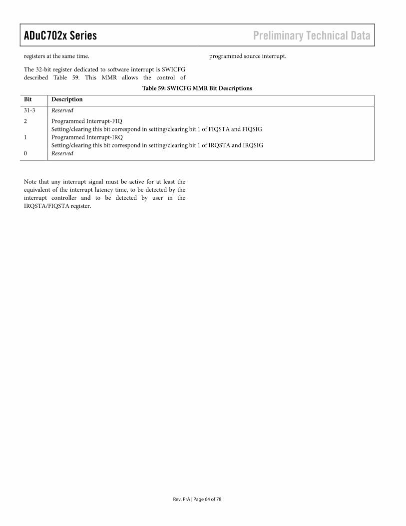
ADuC702x Series Preliminary Technical Data
Rev. PrA | Page 64 of 78
registers at the same time.
The 32-bit register dedicated to software interrupt is SWICFG described Table 59. This MMR allows the control of
programmed source interrupt.
Table 59: SWICFG MMR Bit Descriptions
Bit Description
31-3 Reserved
2 Programmed Interrupt-FIQ Setting/clearing this bit correspond in setting/clearing bit 1 of FIQSTA and FIQSIG
1 Programmed Interrupt-IRQ Setting/clearing this bit correspond in setting/clearing bit 1 of IRQSTA and IRQSIG
0 Reserved
Note that any interrupt signal must be active for at least the equivalent of the interrupt latency time, to be detected by the interrupt controller and to be detected by user in the IRQSTA/FIQSTA register.
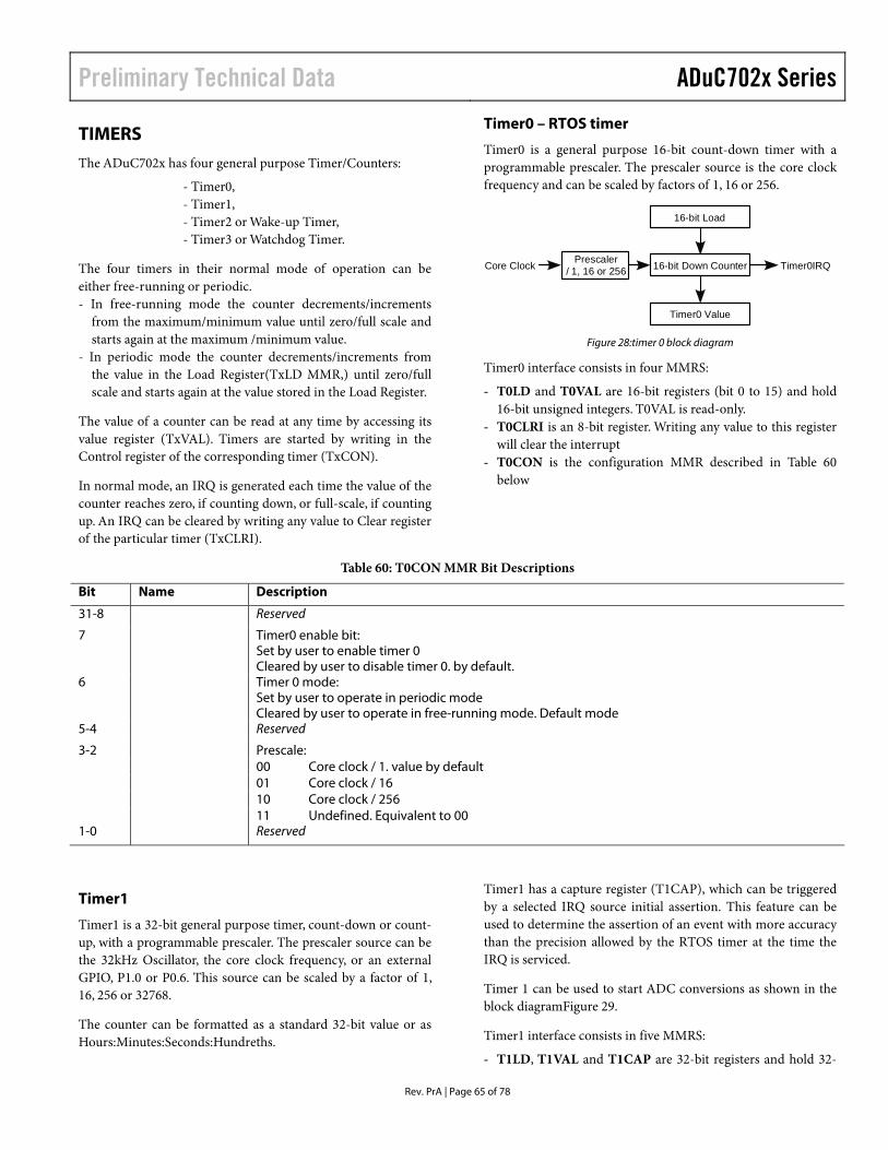
Preliminary Technical Data ADuC702x Series
Rev. PrA | Page 65 of 78
TIMERS
The ADuC702x has four general purpose Timer/Counters:
- Timer0, - Timer1, - Timer2 or Wake-up Timer, - Timer3 or Watchdog Timer.
The four timers in their normal mode of operation can be either free-running or periodic. - In free-running mode the counter decrements/increments
from the maximum/minimum value until zero/full scale and starts again at the maximum /minimum value.
- In periodic mode the counter decrements/increments from the value in the Load Register(TxLD MMR,) until zero/full scale and starts again at the value stored in the Load Register.
The value of a counter can be read at any time by accessing its value register (TxVAL). Timers are started by writing in the Control register of the corresponding timer (TxCON).
In normal mode, an IRQ is generated each time the value of the counter reaches zero, if counting down, or full-scale, if counting up. An IRQ can be cleared by writing any value to Clear register of the particular timer (TxCLRI).
Timer0 – RTOS timer
Timer0 is a general purpose 16-bit count-down timer with a programmable prescaler. The prescaler source is the core clock frequency and can be scaled by factors of 1, 16 or 256.
Core Clock 16-bit Down Counter
Timer0 Value
16-bit Load
Timer0IRQPrescaler/ 1, 16 or 256
Figure 28:timer 0 block diagram
Timer0 interface consists in four MMRS:
- T0LD and T0VAL are 16-bit registers (bit 0 to 15) and hold 16-bit unsigned integers. T0VAL is read-only.
- T0CLRI is an 8-bit register. Writing any value to this register will clear the interrupt
- T0CON is the configuration MMR described in Table 60 below
Table 60: T0CON MMR Bit Descriptions
Bit Name Description
31-8 Reserved
7 Timer0 enable bit: Set by user to enable timer 0 Cleared by user to disable timer 0. by default.
6 Timer 0 mode: Set by user to operate in periodic mode Cleared by user to operate in free-running mode. Default mode
5-4 Reserved
Prescale: 00 Core clock / 1. value by default 01 Core clock / 16 10 Core clock / 256
3-2
11 Undefined. Equivalent to 00 1-0 Reserved
Timer1
Timer1 is a 32-bit general purpose timer, count-down or count-up, with a programmable prescaler. The prescaler source can be the 32kHz Oscillator, the core clock frequency, or an external GPIO, P1.0 or P0.6. This source can be scaled by a factor of 1, 16, 256 or 32768.
The counter can be formatted as a standard 32-bit value or as Hours:Minutes:Seconds:Hundreths.
Timer1 has a capture register (T1CAP), which can be triggered by a selected IRQ source initial assertion. This feature can be used to determine the assertion of an event with more accuracy than the precision allowed by the RTOS timer at the time the IRQ is serviced.
Timer 1 can be used to start ADC conversions as shown in the block diagramFigure 29.
Timer1 interface consists in five MMRS:
- T1LD, T1VAL and T1CAP are 32-bit registers and hold 32-
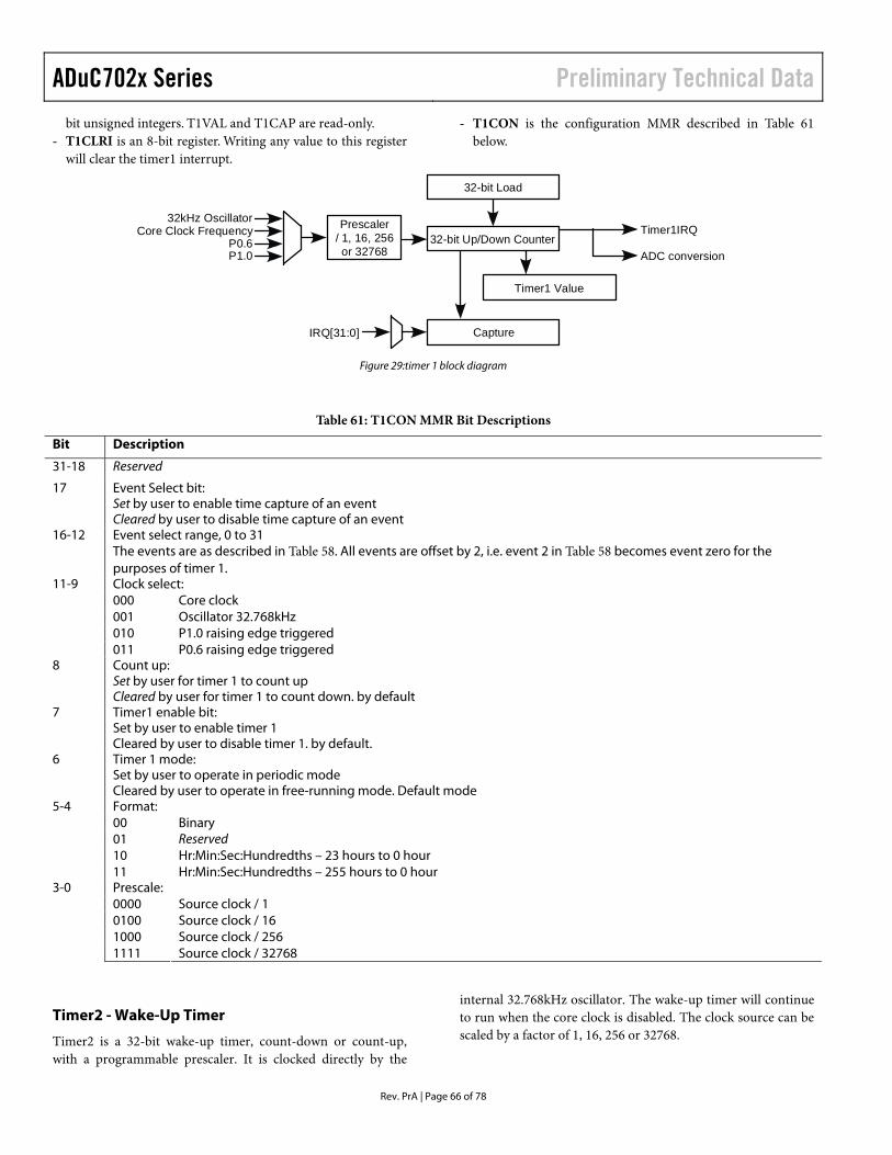
ADuC702x Series Preliminary Technical Data
Rev. PrA | Page 66 of 78
bit unsigned integers. T1VAL and T1CAP are read-only. - T1CLRI is an 8-bit register. Writing any value to this register
will clear the timer1 interrupt.
- T1CON is the configuration MMR described in Table 61 below.
Prescaler/ 1, 16, 256or 32768
32kHz OscillatorCore Clock Frequency
P0.6P1.0
Timer1IRQ32-bit Up/Down Counter
32-bit Load
CaptureIRQ[31:0]
Timer1 Value
ADC conversion
Figure 29:timer 1 block diagram
Table 61: T1CON MMR Bit Descriptions
Bit Description
31-18 Reserved
17 Event Select bit: Set by user to enable time capture of an event Cleared by user to disable time capture of an event
16-12 Event select range, 0 to 31 The events are as described in Table 58. All events are offset by 2, i.e. event 2 in Table 58 becomes event zero for the purposes of timer 1. Clock select: 000 Core clock 001 Oscillator 32.768kHz 010 P1.0 raising edge triggered
11-9
011 P0.6 raising edge triggered 8 Count up:
Set by user for timer 1 to count up Cleared by user for timer 1 to count down. by default
7 Timer1 enable bit: Set by user to enable timer 1 Cleared by user to disable timer 1. by default.
6 Timer 1 mode: Set by user to operate in periodic mode Cleared by user to operate in free-running mode. Default mode Format: 00 Binary 01 Reserved 10 Hr:Min:Sec:Hundredths – 23 hours to 0 hour
5-4
11 Hr:Min:Sec:Hundredths – 255 hours to 0 hour Prescale: 0000 Source clock / 1 0100 Source clock / 16 1000 Source clock / 256
3-0
1111 Source clock / 32768
Timer2 - Wake-Up Timer
Timer2 is a 32-bit wake-up timer, count-down or count-up, with a programmable prescaler. It is clocked directly by the
internal 32.768kHz oscillator. The wake-up timer will continue to run when the core clock is disabled. The clock source can be scaled by a factor of 1, 16, 256 or 32768.
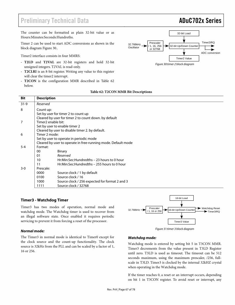
Preliminary Technical Data ADuC702x Series
Rev. PrA | Page 67 of 78
The counter can be formatted as plain 32-bit value or as Hours:Minutes:Seconds:Hundreths.
Timer 2 can be used to start ADC conversions as shown in the block diagram Figure 30..
Timer2 interface consists in four MMRS:
- T2LD and T2VAL are 32-bit registers and hold 32-bit unsigned integers. T2VAL is read-only.
- T2CLRI is an 8-bit register. Writing any value to this register will clear the timer2 interrupt.
- T2CON is the configuration MMR described in Table 62 below.
32.768kHzOscillator
Prescaler/ 1, 16, 256or 32768
32-bit Up/Down CounterTimer2IRQ
32-bit Load
Timer2 Value
ADC conversion
Figure 30:timer 2 block diagram
Table 62: T2CON MMR Bit Descriptions
Bit Description
31-9 Reserved
8 Count up: Set by user for timer 2 to count up Cleared by user for timer 2 to count down. by default
7 Timer2 enable bit: Set by user to enable timer 2 Cleared by user to disable timer 2. by default.
6 Timer 2 mode: Set by user to operate in periodic mode Cleared by user to operate in free-running mode. Default mode Format: 00 Binary 01 Reserved 10 Hr:Min:Sec:Hundredths – 23 hours to 0 hour
5-4
11 Hr:Min:Sec:Hundredths – 255 hours to 0 hour Prescale: 0000 Source clock / 1 by default 0100 Source clock / 16 1000 Source clock / 256 expected for format 2 and 3
3-0
1111 Source clock / 32768
Timer3 - Watchdog Timer
Timer3 has two modes of operation, normal mode and watchdog mode. The Watchdog timer is used to recover from an illegal software state. Once enabled it requires periodic servicing to prevent it from forcing a reset of the processor.
Normal mode:
The Timer3 in normal mode is identical to Timer0 except for the clock source and the count-up functionality. The clock source is 32kHz from the PLL and can be scaled by a factor of 1, 16 or 256.
16-bit Up/Down Counter
16-bit Load
Timer3IRQWatchdog Reset
Timer3 Value
32.768kHzPrescaler
/ 1, 16 or 256
Figure 31:timer 3 block diagram
Watchdog mode:
Watchdog mode is entered by setting bit 5 in T3CON MMR. Timer3 decrements from the value present in T3LD Register until zero. T3LD is used as timeout. The timeout can be 512 seconds maximum, using the maximum prescaler, /256, full-scale in T3LD. Timer3 is clocked by the internal 32kHZ crystal when operating in the Watchdog mode.
If the timer reaches 0, a reset or an interrupt occurs, depending on bit 1 in T3CON register. To avoid reset or interrupt, any
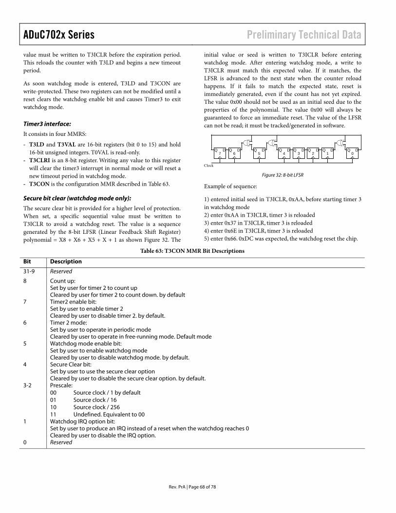
ADuC702x Series Preliminary Technical Data
Rev. PrA | Page 68 of 78
value must be written to T3ICLR before the expiration period. This reloads the counter with T3LD and begins a new timeout period.
As soon watchdog mode is entered, T3LD and T3CON are write-protected. These two registers can not be modified until a reset clears the watchdog enable bit and causes Timer3 to exit watchdog mode.
Timer3 interface:
It consists in four MMRS:
- T3LD and T3VAL are 16-bit registers (bit 0 to 15) and hold 16-bit unsigned integers. T0VAL is read-only.
- T3CLRI is an 8-bit register. Writing any value to this register will clear the timer3 interrupt in normal mode or will reset a new timeout period in watchdog mode.
- T3CON is the configuration MMR described in Table 63.
Secure bit clear (watchdog mode only):
The secure clear bit is provided for a higher level of protection. When set, a specific sequential value must be written to T3ICLR to avoid a watchdog reset. The value is a sequence generated by the 8-bit LFSR (Linear Feedback Shift Register) polynomial = X8 + X6 + X5 + X + 1 as shown Figure 32. The
initial value or seed is written to T3ICLR before entering watchdog mode. After entering watchdog mode, a write to T3ICLR must match this expected value. If it matches, the LFSR is advanced to the next state when the counter reload happens. If it fails to match the expected state, reset is immediately generated, even if the count has not yet expired. The value 0x00 should not be used as an initial seed due to the properties of the polynomial. The value 0x00 will always be guaranteed to force an immediate reset. The value of the LFSR can not be read; it must be tracked/generated in software.
DQ6
DQ0
DQ1
DQ2
DQ3
DQ7
DQ4
DQ5
Clock Figure 32: 8-bit LFSR
Example of sequence:
1) entered initial seed in T3ICLR, 0xAA, before starting timer 3 in watchdog mode 2) enter 0xAA in T3ICLR, timer 3 is reloaded 3) enter 0x37 in T3ICLR, timer 3 is reloaded 4) enter 0x6E in T3ICLR, timer 3 is reloaded 5) enter 0x66. 0xDC was expected, the watchdog reset the chip.
Table 63: T3CON MMR Bit Descriptions
Bit Description
31-9 Reserved
8 Count up: Set by user for timer 2 to count up Cleared by user for timer 2 to count down. by default
7 Timer2 enable bit: Set by user to enable timer 2 Cleared by user to disable timer 2. by default.
6 Timer 2 mode: Set by user to operate in periodic mode Cleared by user to operate in free-running mode. Default mode
5 Watchdog mode enable bit: Set by user to enable watchdog mode Cleared by user to disable watchdog mode. by default.
4 Secure Clear bit: Set by user to use the secure clear option Cleared by user to disable the secure clear option. by default. Prescale: 00 Source clock / 1 by default 01 Source clock / 16 10 Source clock / 256
3-2
11 Undefined. Equivalent to 00 1 Watchdog IRQ option bit:
Set by user to produce an IRQ instead of a reset when the watchdog reaches 0 Cleared by user to disable the IRQ option.
0 Reserved
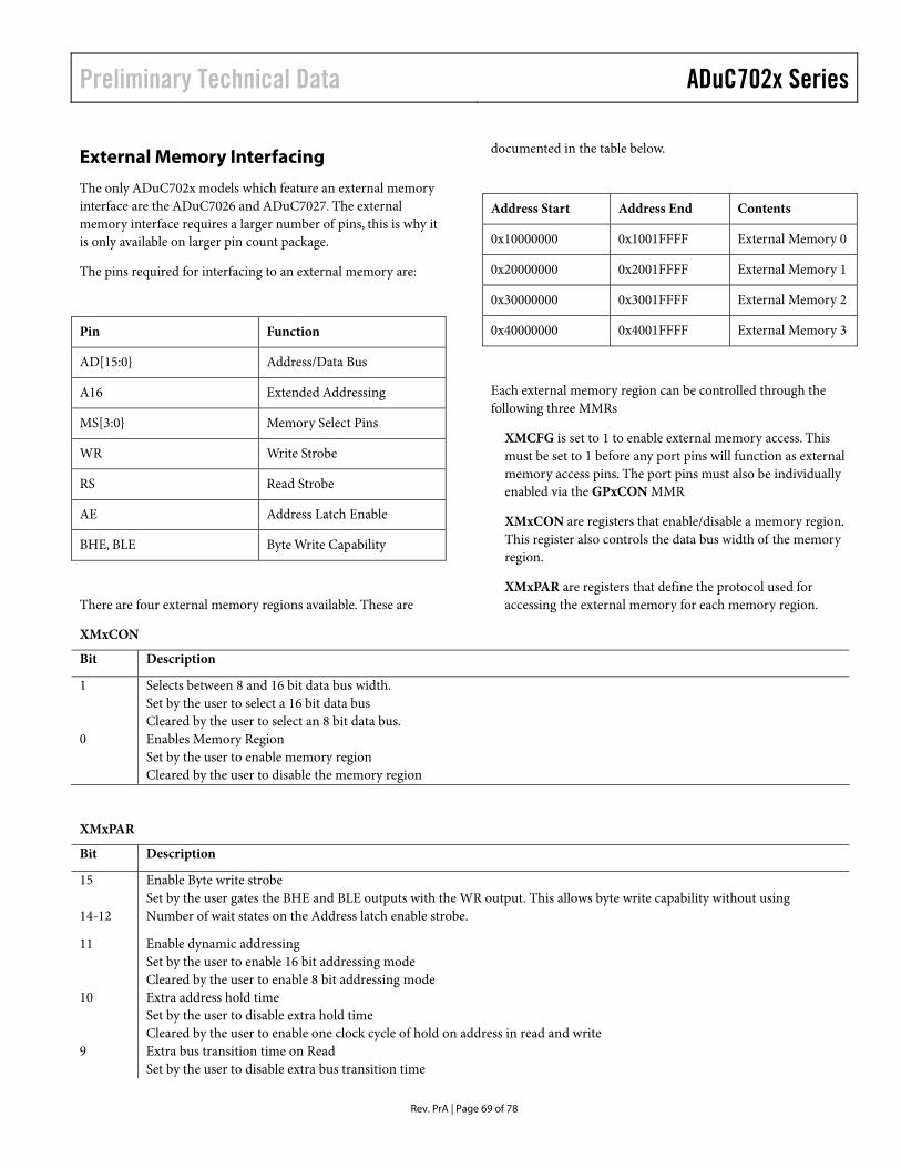
Preliminary Technical Data ADuC702x Series
Rev. PrA | Page 69 of 78
External Memory Interfacing
The only ADuC702x models which feature an external memory interface are the ADuC7026 and ADuC7027. The external memory interface requires a larger number of pins, this is why it is only available on larger pin count package.
The pins required for interfacing to an external memory are:
Pin Function
AD[15:0 Address/Data Bus
A16 Extended Addressing
MS[3:0 Memory Select Pins
WR Write Strobe
RS Read Strobe
AE Address Latch Enable
BHE, BLE Byte Write Capability
There are four external memory regions available. These are
documented in the table below.
Address Start Address End Contents
0x10000000 0x1001FFFF External Memory 0
0x20000000 0x2001FFFF External Memory 1
0x30000000 0x3001FFFF External Memory 2
0x40000000 0x4001FFFF External Memory 3
Each external memory region can be controlled through the following three MMRs
XMCFG is set to 1 to enable external memory access. This must be set to 1 before any port pins will function as external memory access pins. The port pins must also be individually enabled via the GPxCON MMR
XMxCON are registers that enable/disable a memory region. This register also controls the data bus width of the memory region.
XMxPAR are registers that define the protocol used for accessing the external memory for each memory region.
XMxCON
Bit Description
1 Selects between 8 and 16 bit data bus width. Set by the user to select a 16 bit data bus Cleared by the user to select an 8 bit data bus.
0 Enables Memory Region Set by the user to enable memory region Cleared by the user to disable the memory region
XMxPAR
Bit Description
15 Enable Byte write strobe Set by the user gates the BHE and BLE outputs with the WR output. This allows byte write capability without using
14-12 Number of wait states on the Address latch enable strobe.
11 Enable dynamic addressing Set by the user to enable 16 bit addressing mode Cleared by the user to enable 8 bit addressing mode
10 Extra address hold time Set by the user to disable extra hold time Cleared by the user to enable one clock cycle of hold on address in read and write
9 Extra bus transition time on Read Set by the user to disable extra bus transition time
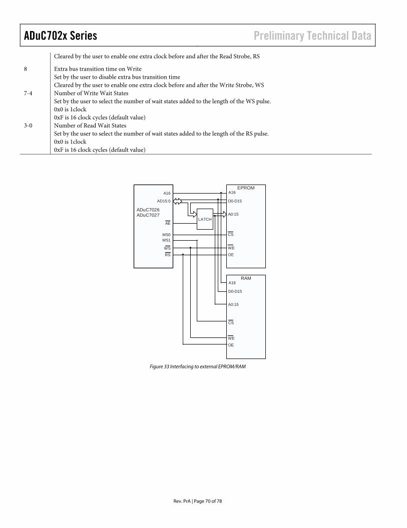
ADuC702x Series Preliminary Technical Data
Rev. PrA | Page 70 of 78
Cleared by the user to enable one extra clock before and after the Read Strobe, RS
8 Extra bus transition time on Write Set by the user to disable extra bus transition time Cleared by the user to enable one extra clock before and after the Write Strobe, WS
7-4 Number of Write Wait States Set by the user to select the number of wait states added to the length of the WS pulse. 0x0 is 1clock 0xF is 16 clock cycles (default value)
3-0 Number of Read Wait States Set by the user to select the number of wait states added to the length of the RS pulse. 0x0 is 1clock 0xF is 16 clock cycles (default value)
LATCH
EPROM
OE
A0:15
D0-D15
A16
WE
ADuC7026ADuC7027
RS
AE
AD15:0
A16
WS
MS0MS1
RAM
OE
A0:15
D0-D15
A16
WE
CS
CS
Figure 33 Interfacing to external EPROM/RAM
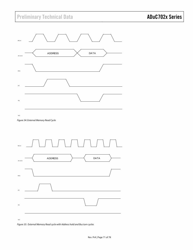
Preliminary Technical Data ADuC702x Series
Rev. PrA | Page 71 of 78
AE
RS
WS
MCLK
AD 16:0
MSx
ADDRESS DATA
Figure 34: External Memory Read Cycle
AE
RS
WS
MCLK
AD 16:0
MSx
ADDRESS DATA
Figure 35: External Memory Read cycle with Address hold and Bus turn cycles
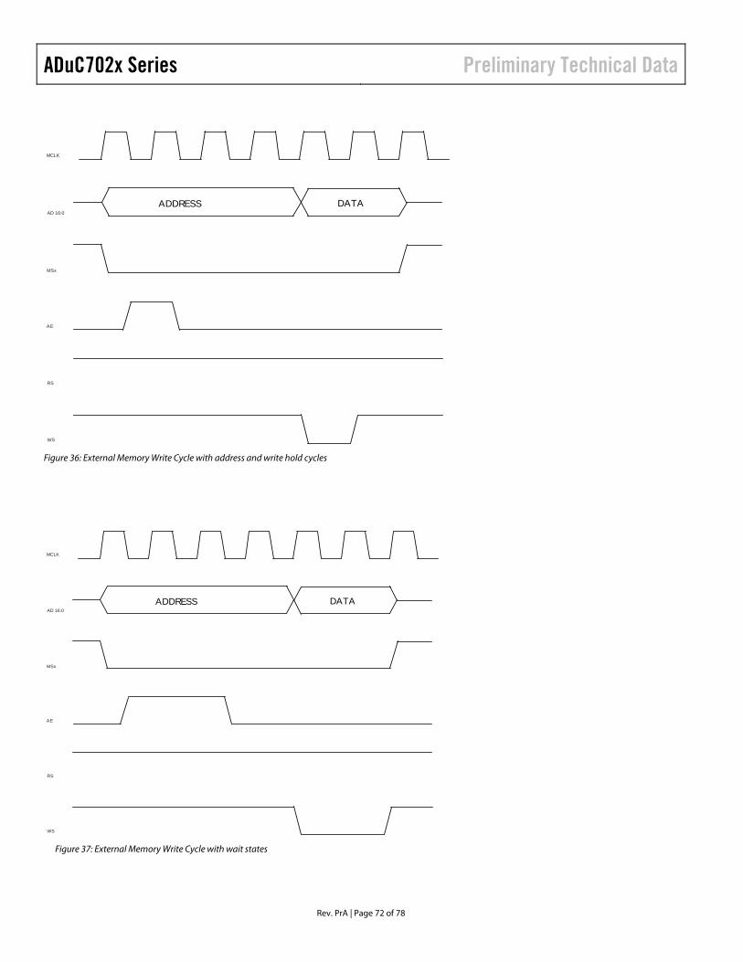
ADuC702x Series Preliminary Technical Data
Rev. PrA | Page 72 of 78
AE
RS
WS
MCLK
AD 16:0
MSx
ADDRESS DATA
Figure 36: External Memory Write Cycle with address and write hold cycles
AE
RS
WS
MCLK
AD 16:0
MSx
ADDRESS DATA
Figure 37: External Memory Write Cycle with wait states
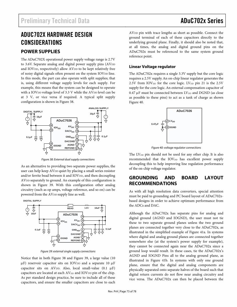
Preliminary Technical Data ADuC702x Series
Rev. PrA | Page 73 of 78
ADUC702X HARDWARE DESIGN CONSIDERATIONS POWER SUPPLIES
The ADuC702X operational power supply voltage range is 2.7V to 3.6V. Separate analog and digital power supply pins (AVDD
and IOVDD, respectively) allow AVDD to be kept relatively free of noisy digital signals often present on the system IOVDD line. In this mode, the part can also operate with split supplies; that is, using different voltage supply levels for each supply. For example, this means that the system can be designed to operate with a IOVDD voltage level of 3.3 V while the AVDD level can be at 3 V, or vice versa if required. A typical split supply configuration is shown in Figure 38.
IOVDD
ADuC7026
AGND
AVDD
-+
0.1µF
10µF
ANALOG SUPPLY
10µF
IOGND
0.1µF
DIGITAL SUPPLY
-+
GNDREF
DACVDD
DACGND
REFGND
Figure 38: External dual supply connections
As an alternative to providing two separate power supplies, the user can help keep AVDD quiet by placing a small series resistor and/or ferrite bead between it and IOVDD, and then decoupling AVDD separately to ground. An example of this configuration is shown in Figure 39. With this configuration other analog circuitry (such as op amps, voltage reference, and so on) can be powered from the AVDD supply line as well.
IOVDD
ADuC7026
AGND
AVDD
0.1uF
IOGND
0.1uF GNDREF
DACVDD
DACGND
REFGND
10uF-+ 10uF1.6VBEAD
DIGITAL SUPPLY
Figure 39: external single supply connections
Notice that in both Figure 38 and Figure 39, a large value (10 µF) reservoir capacitor sits on IOVDD and a separate 10 µF capacitor sits on AVDD. Also, local small-value (0.1 µF) capacitors are located at each AVDD and IOVDD pin of the chip. As per standard design practice, be sure to include all of these capacitors, and ensure the smaller capacitors are close to each
AVDD pin with trace lengths as short as possible. Connect the ground terminal of each of these capacitors directly to the underlying ground plane. Finally, it should also be noted that, at all times, the analog and digital ground pins on the ADuC702x must be referenced to the same system ground reference point.
Linear Voltage regulator
The ADuC702x requires a single 3.3V supply but the core logic requires a 2.5V supply. An on-chip linear regulator generates the 2.5V from IOVDD for the core logic. LVDD pin 21 is the 2.5V supply for the core logic. An external compensation capacitor of 0.47 µF must be connected between LVDD and DGND (as close as possible to these pins) to act as a tank of charge as shown Figure 40.
ADuC7026
0.47µFDGND
LVDD
Figure 40: voltage regulator connections
The LVDD pin should not be used for any other chip. It is also recommended that the IOVDD has excellent power supply decoupling this to help improving line regulation performance of the on-chip voltage regulator.
GROUNDING AND BOARD LAYOUT RECOMMENDATIONS
As with all high resolution data converters, special attention must be paid to grounding and PC board layout of ADuC702x-based designs in order to achieve optimum performance from the ADCs and DAC.
Although the ADuC702x has separate pins for analog and digital ground (AGND and IOGND), the user must not tie these to two separate ground planes unless the two ground planes are connected together very close to the ADuC702x, as illustrated in the simplified example of Figure 41a. In systems where digital and analog ground planes are connected together somewhere else (at the system’s power supply for example), they cannot be connected again near the ADuC702x since a ground loop would result. In these cases, tie the ADuC702x’s AGND and IOGND Pins all to the analog ground plane, as illustrated in Figure 41b. In systems with only one ground plane, ensure that the digital and analog components are physically separated onto separate halves of the board such that digital return currents do not flow near analog circuitry and vice versa. The ADuC702x can then be placed between the
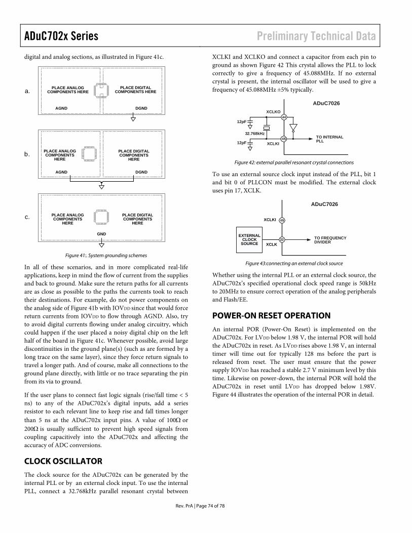
ADuC702x Series Preliminary Technical Data
Rev. PrA | Page 74 of 78
digital and analog sections, as illustrated in Figure 41c.
b.
DGNDAGND
PLACE ANALOGCOMPONENTS
HERE
PLACE DIGITALCOMPONENTS
HERE
c.
GND
PLACE ANALOGCOMPONENTS
HERE
PLACE DIGITALCOMPONENTS
HERE
DGND
PLACE ANALOGCOMPONENTS HEREa.
AGND
PLACE DIGITALCOMPONENTS HERE
Figure 41:. System grounding schemes
In all of these scenarios, and in more complicated real-life applications, keep in mind the flow of current from the supplies and back to ground. Make sure the return paths for all currents are as close as possible to the paths the currents took to reach their destinations. For example, do not power components on the analog side of Figure 41b with IOVDD since that would force return currents from IOVDD to flow through AGND. Also, try to avoid digital currents flowing under analog circuitry, which could happen if the user placed a noisy digital chip on the left half of the board in Figure 41c. Whenever possible, avoid large discontinuities in the ground plane(s) (such as are formed by a long trace on the same layer), since they force return signals to travel a longer path. And of course, make all connections to the ground plane directly, with little or no trace separating the pin from its via to ground.
If the user plans to connect fast logic signals (rise/fall time < 5 ns) to any of the ADuC702x’s digital inputs, add a series resistor to each relevant line to keep rise and fall times longer than 5 ns at the ADuC702x input pins. A value of 100Ω or 200Ω is usually sufficient to prevent high speed signals from coupling capacitively into the ADuC702x and affecting the accuracy of ADC conversions.
CLOCK OSCILLATOR
The clock source for the ADuC702x can be generated by the internal PLL or by an external clock input. To use the internal PLL, connect a 32.768kHz parallel resonant crystal between
XCLKI and XCLKO and connect a capacitor from each pin to ground as shown Figure 42 This crystal allows the PLL to lock correctly to give a frequency of 45.088MHz. If no external crystal is present, the internal oscillator will be used to give a frequency of 45.088MHz ±5% typically.
12pF XCLKI
XCLKO
32.768kHzTO INTERNALPLL
ADuC7026
12pF
Figure 42: external parallel resonant crystal connections
To use an external source clock input instead of the PLL, bit 1 and bit 0 of PLLCON must be modified. The external clock uses pin 17, XCLK.
TO FREQUENCYDIVIDER
ADuC7026
XCLK
EXTERNALCLOCK
SOURCE
XCLKI
Figure 43:connecting an external clock source
Whether using the internal PLL or an external clock source, the ADuC702x’s specified operational clock speed range is 50kHz to 20MHz to ensure correct operation of the analog peripherals and Flash/EE.
POWER-ON RESET OPERATION
An internal POR (Power-On Reset) is implemented on the ADuC702x. For LVDD below 1.98 V, the internal POR will hold the ADuC702x in reset. As LVDD rises above 1.98 V, an internal timer will time out for typically 128 ms before the part is released from reset. The user must ensure that the power supply IOVDD has reached a stable 2.7 V minimum level by this time. Likewise on power-down, the internal POR will hold the ADuC702x in reset until LVDD has dropped below 1.98V. Figure 44 illustrates the operation of the internal POR in detail.
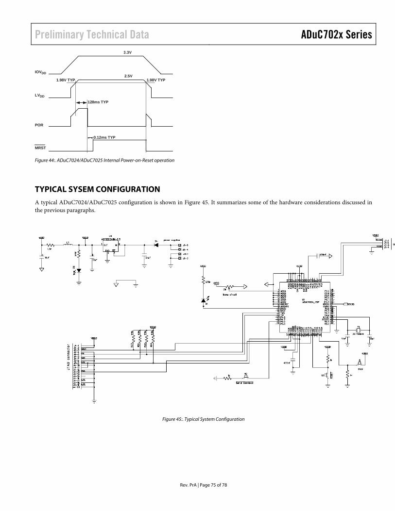
Preliminary Technical Data ADuC702x Series
Rev. PrA | Page 75 of 78
128ms TYP
1.98V TYP
IOVDD
3.3V
LVDD
2.5V1.98V TYP
0.12ms TYP
POR
MRST
Figure 44:. ADuC7024/ADuC7025 Internal Power-on-Reset operation
TYPICAL SYSEM CONFIGURATION
A typical ADuC7024/ADuC7025 configuration is shown in Figure 45. It summarizes some of the hardware considerations discussed in the previous paragraphs.
Figure 45:. Typical System Configuration
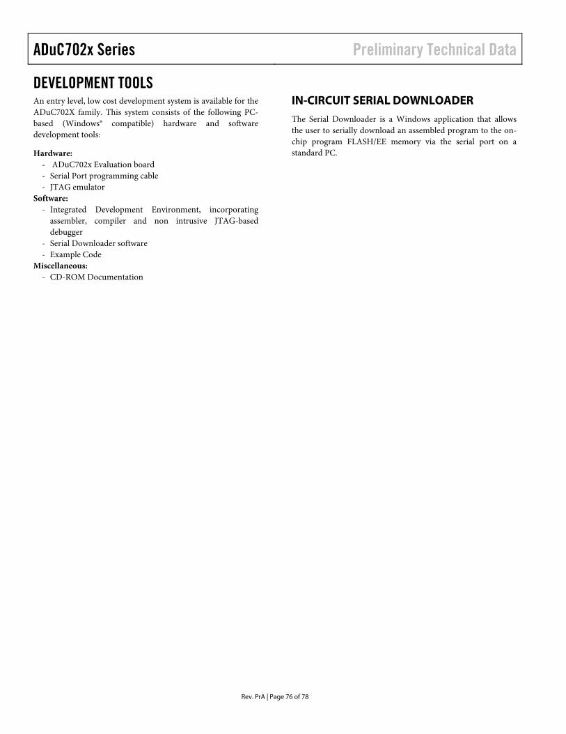
ADuC702x Series Preliminary Technical Data
Rev. PrA | Page 76 of 78
DEVELOPMENT TOOLS
An entry level, low cost development system is available for the ADuC702X family. This system consists of the following PC-based (Windows® compatible) hardware and software development tools:
Hardware: - ADuC702x Evaluation board - Serial Port programming cable - JTAG emulator
Software: - Integrated Development Environment, incorporating
assembler, compiler and non intrusive JTAG-based debugger
- Serial Downloader software - Example Code
Miscellaneous: - CD-ROM Documentation
IN-CIRCUIT SERIAL DOWNLOADER
The Serial Downloader is a Windows application that allows the user to serially download an assembled program to the on-chip program FLASH/EE memory via the serial port on a standard PC.
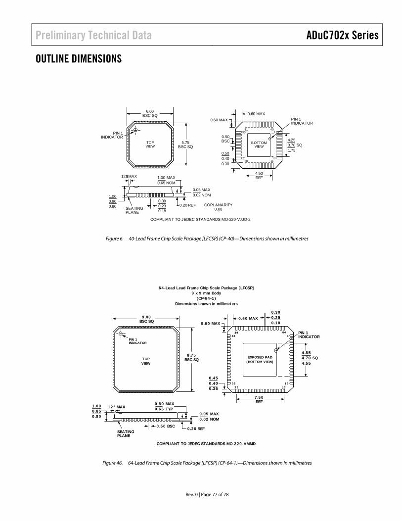
Preliminary Technical Data ADuC702x Series
Rev. 0 | Page 77 of 78
OUTLINE DIMENSIONS
140
1011
3130
2120
BOTTOMVIEW
4.253.70 SQ1.75
TOPVIEW
6.00BSC SQ
PIN 1INDICATOR
5.75BSC SQ
128MAX
0.300.230.18
0.20 REFSEATINGPLANE
1.000.900.80
0.05 MAX0.02 NOM
COPLANARITY0.08
1.00 MAX0.65 NOM
4.50REF
0.500.400.30
0.50BSC
PIN 1INDICATOR
0.60 MAX0.60 MAX
COMPLIANT TO JEDEC STANDARDS MO-220-VJJD-2
Figure 6. 40-Lead Frame Chip Scale Package [LFCSP] (CP-40)—Dimensions shown in millimetres
PIN 1INDICATOR
TOPVIEW
8.75BSC SQ
9.00BSC SQ
164
1 617
4948
3 233
0 .450 .400 .35
0 .50 BSC 0.20 REF
12 ° MAX0.80 MAX0.65 TYP
1.000 .850 .80
7 .50REF
0.05 MAX0.02 NOM
0.60 MAX0.60 MAX
4.854 .70 SQ4.55
SEATINGPLANE
PIN 1INDICATOR
EXPOSED PAD( BOTTOM VIEW)
0 .300 .250 .18
64-Lead Lead Frame Chip Scale Package [LFCSP]9 x 9 mm Body
(CP-64-1 )Dimensions shown in millimeters
COMPLIANT TO JEDEC STANDARDS MO-220-VMMD
Figure 46. 64-Lead Frame Chip Scale Package [LFCSP] (CP-64-1)—Dimensions shown in millimetres
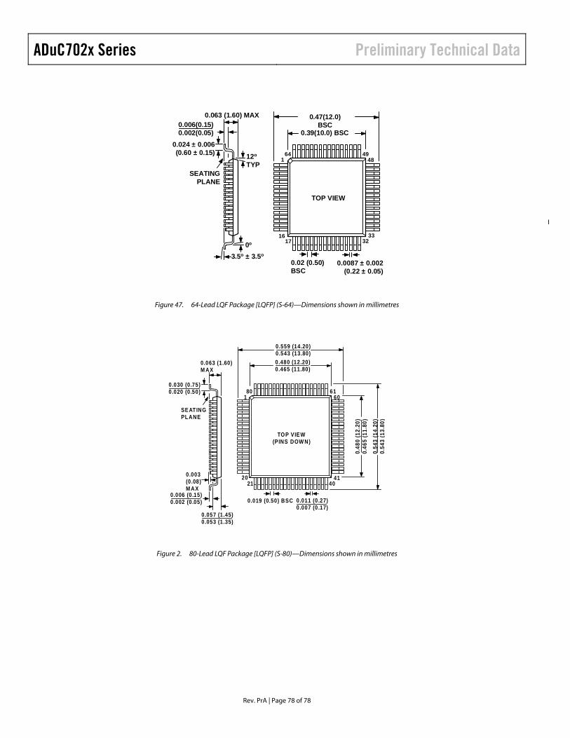
ADuC702x Series Preliminary Technical Data
Rev. PrA | Page 78 of 78
1
1617
3332
484964
TOP VIEW
0.47(12.0)BSC
0.39(10.0) BSC
0.02 (0.50)BSC
0.0087 ± 0.002(0.22 ± 0.05)
SEATINGPLANE
0.063 (1.60) MAX
0.024 ± 0.006(0.60 ± 0.15) 12o
TYP
0o
3.5o ± 3.5o
0.006(0.15)0.002(0.05)
Figure 47. 64-Lead LQF Package [LQFP] (S-64)—Dimensions shown in millimetres
SE ATINGPLANE
0.063 (1.60)M AX
0.030 (0.75)0.020 (0.50)
0.003(0.08)M AX
0.057 (1.45)0.053 (1.35)
0.006 (0.15)0.002 (0.05) 0.011 (0.27)
0.007 (0.17)
0.559 (14.20)0.543 (13.80)0.480 (12.20)0.465 (11.80)
0.48
0(1
2.20
)0.
465
(11.
80)
0.54
3(1
4.20
)0.
543
(13.
80)
1
2021
4140
606180
TOP VIE W(PINS DOW N)
0.019 (0.50) BSC
Figure 2. 80-Lead LQF Package [LQFP] (S-80)—Dimensions shown in millimetres