
ADuCM320i (Rev. A) - analog.com · Precision Analog Microcontroller, 14-Bit Analog I/O with MDIO...
26
Precision Analog Microcontroller, 14-Bit Analog I/O with MDIO Interface, Arm Cortex-M3 Data Sheet ADuCM320i Rev. A Document Feedback Information furnished by Analog Devices is believed to be accurate and reliable. However, no responsibility is assumed by Analog Devices for its use, nor for any infringements of patents or other rights of third parties that may result from its use. Specifications subject to change without notice. No license is granted by implication or otherwise under any patent or patent rights of Analog Devices. Trademarks and registered trademarks are the property of their respective owners. One Technology Way, P.O. Box 9106, Norwood, MA 02062-9106, U.S.A. Tel: 781.329.4700 ©2015–2018 Analog Devices, Inc. All rights reserved. Technical Support www.analog.com FEATURES Analog input/output Multichannel, 14-bit, 1 MSPS analog-to-digital converter (ADC) Up to 16 ADC input channels 0 V to VREF analog input range Fully differential and single-ended modes AVDD and IOVDD monitors 12-bit voltage output digital-to-analog converters (VDACs) 8 VDACs with a range of 0 V to 2.5 V or AVDD outputs 12-bit current output DACs (IDACs) 4 IDACS with a range of 0 mA to 150 mA outputs Voltage comparator Microcontroller Arm Cortex-M3 processor, 32-bit RISC architecture Serial wire port supports code download and debug Clocking options 80 MHz PLL with programmable divider Trimmed on-chip oscillator (±3%) External 16 MHz crystal option External clock source up to 80 MHz Memory 2 × 128 kB independent Flash/EE memories 10,000 cycle Flash/EE endurance 20-year Flash/EE retention 32 kB SRAM In circuit reprogrammability via I 2 C On-chip peripherals MDIO slave up to 4 MHz 2 × I 2 C, 2 × SPI, UART Multiple general-purpose input/output (GPIO) pins: 3.6 V compliant 7 × 1.2 V compatible when used for MDIO 32-element programmable logic array (PLA) 3 general-purpose timers Wake-up timer Watchdog timer 16-bit pulse width modulator (PWM) Power Supply range: 2.9 V to 3.6 V, and 1.8 V to 2.5 V for IDACs Flexible operating modes for low power applications Package and temperature range 6 mm × 6mm, 96-ball CSP_BGA package Fully specified for −40°C to +105°C ambient operation Tools Low cost QuickStart development system Full third party support APPLICATIONS Optical networking
Transcript of ADuCM320i (Rev. A) - analog.com · Precision Analog Microcontroller, 14-Bit Analog I/O with MDIO...
Precision Analog Microcontroller, 14-Bit Analog I/O with MDIO Interface, Arm Cortex-M3
Data Sheet ADuCM320i
Rev. A Document Feedback Information furnished by Analog Devices is believed to be accurate and reliable. However, no responsibility is assumed by Analog Devices for its use, nor for any infringements of patents or other rights of third parties that may result from its use. Specifications subject to change without notice. No license is granted by implication or otherwise under any patent or patent rights of Analog Devices. Trademarks and registered trademarks are the property of their respective owners.
One Technology Way, P.O. Box 9106, Norwood, MA 02062-9106, U.S.A. Tel: 781.329.4700 ©2015–2018 Analog Devices, Inc. All rights reserved. Technical Support www.analog.com
FEATURES Analog input/output
Multichannel, 14-bit, 1 MSPS analog-to-digital converter (ADC) Up to 16 ADC input channels 0 V to VREF analog input range Fully differential and single-ended modes AVDD and IOVDD monitors
12-bit voltage output digital-to-analog converters (VDACs) 8 VDACs with a range of 0 V to 2.5 V or AVDD outputs
12-bit current output DACs (IDACs) 4 IDACS with a range of 0 mA to 150 mA outputs
Voltage comparator Microcontroller
Arm Cortex-M3 processor, 32-bit RISC architecture Serial wire port supports code download and debug
Clocking options 80 MHz PLL with programmable divider Trimmed on-chip oscillator (±3%) External 16 MHz crystal option External clock source up to 80 MHz
Memory 2 × 128 kB independent Flash/EE memories 10,000 cycle Flash/EE endurance 20-year Flash/EE retention 32 kB SRAM
In circuit reprogrammability via I2C
On-chip peripherals MDIO slave up to 4 MHz 2 × I2C, 2 × SPI, UART Multiple general-purpose input/output (GPIO) pins: 3.6 V
compliant 7 × 1.2 V compatible when used for MDIO 32-element programmable logic array (PLA) 3 general-purpose timers Wake-up timer Watchdog timer 16-bit pulse width modulator (PWM)
Power Supply range: 2.9 V to 3.6 V, and 1.8 V to 2.5 V for IDACs Flexible operating modes for low power applications
Package and temperature range 6 mm × 6mm, 96-ball CSP_BGA package Fully specified for −40°C to +105°C ambient operation
Tools Low cost QuickStart development system Full third party support
APPLICATIONS Optical networking
ADuCM320i Data Sheet
Rev. A | Page 2 of 26
TABLE OF CONTENTS Features .............................................................................................. 1 Applications ....................................................................................... 1 Revision History ............................................................................... 2 Functional Block Diagram .............................................................. 3 General Description ......................................................................... 4 Specifications ..................................................................................... 5
Microcontroller Electrical Specifications .................................. 5 Timing Specifications ................................................................ 11 Absolute Maximum Ratings ..................................................... 17
ESD Caution................................................................................ 17 Pin Configuration and Function Descriptions ........................... 18 Typical Performance Characteristics ........................................... 23 Applications Information .............................................................. 24
Recommended Circuit and Component Values .................... 24 Packaging and Ordering Information ......................................... 26
Outline Dimensions ................................................................... 26 Ordering Guide .......................................................................... 26
REVISION HISTORY 4/2018—Rev. 0 to Rev. A Change to Features Section ............................................................. 1 Change to Microcontroller Electrical Specifications Section ..... 5 Changes to Operating Ambient Temperature Range Parameter and Operating Junction Temperature Range Parameter, Table 9 .............................................................................................. 17 Changes to Ordering Guide .......................................................... 26 8/2015—Revision 0: Initial Version
Data Sheet ADuCM320i
Rev. A | Page 3 of 26
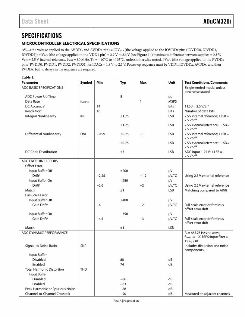
FUNCTIONAL BLOCK DIAGRAM
MEMORY2 × 128kB FLASH
32kB SRAM
ARM CORTEX-M3PROCESSOR
MUX
RESET
AIN0AIN5
AIN6
AIN15
BUF_VREF2V5
VDAC7
IDAC0ADuCM320i
PVDDx
AGNDxIOVDDxIOGNDx
GENERAL-PURPOSEI/O PORTS
SWDIO
SWCLK
GPIO PORTSUART2 × SPI2 × I2C
EXT IRQSMDIOPLA
INTERNALCHANNELS:
TEMPERATURE,AVDD, IOVDD
2.5V BAND GAP
DMANVIC
RESET SYSTEMSERIAL WIRE
CLOCK SYSTEM32.768kHz
16MHz OSC80MHz PLL
3 × GP TIMERWD TIMER
WAKE-UP TIMERPWM
VDAC
IDAC3
14-BITSAR ADC
IDAC
IDAC
COMPA-RATOR
XTALO XTALI ECLKIN
PGND
AVDDxDGNDx
PWM0 TOPWM6
1.8 V LDO
VDAC0 VDAC
1342
2-00
1
Figure 1.
ADuCM320i Data Sheet
Rev. A | Page 4 of 26
GENERAL DESCRIPTION The ADuCM320i is a fully integrated single package device that incorporates high performance analog peripherals together with digital peripherals controlled by an 80 MHz Arm® Cortex™-M3 processor and integral flash for code and data.
The ADC on the ADuCM320i provides 14-bit, 1 MSPS data acquisition on up to 16 input pins that can be programmed for single-ended or differential operation. The voltage at the IDAC output pins can also be measured by the ADC, which is useful for controlling the power consumption of the current DACs. Additionally, chip temperature and supply voltages can be measured.
The ADC input voltage is 0 V to VREF. A sequencer is provided, which allows a user to select a set of ADC channels to be measured in sequence without software involvement during the sequence. The sequence can optionally repeat automatically at a user selectable rate.
Up to eight VDACs are provided with output ranges that are programmable to one of two voltage ranges.
Four IDAC sources are provided. The output currents are programmable with a range of 0 mA to 150 mA. A low drift band gap reference and voltage comparator completes the analog input peripheral set.
The ADuCM320i can be configured so that the digital and analog outputs retain their output voltages and currents through a watchdog or software reset sequence. Thus, a product can remain functional even while the ADuCM320i is resetting itself.
The ADuCM320i has a low power Arm Cortex-M3 processor and a 32-bit RISC machine that offers up to 100 MIPS peak performance. Also integrated on chip are 2 × 128 kB Flash/EE memory and 32 kB of SRAM. The flash comprises two separate 128 kB blocks supporting execution from one flash block and simultaneous writing/erasing of the other flash block.
The ADuCM320i operates from an on-chip oscillator or a 16 MHz external crystal and a PLL at 80 MHz. This clock can optionally be divided down to reduce current consumption. Additional low power modes can be set via software. In normal operating mode, the ADuCM320i digital core consumes about 300 µA per MHz.
The device includes an MDIO interface capable of operating at up to 4 MHz. The capability to simultaneously execute from one flash block and write/erase the other flash block makes the ADuCM320i ideal for 10G, 40G, and 100G optical applications. User programming is eased by incorporating PHYADR and DEVADD hardware comparators. In addition, the nonerasable kernel code plus flags in user flash provide assistance by allowing user code to robustly switch between the two blocks of user flash code and data spaces.
The ADuCM320i integrates a range of on-chip peripherals that can be configured under software control, as required in the appli-cation. These peripherals include 1 × UART, 2 × I2C, and 2 × SPI serial input/output (I/O) communication controllers, GPIO, 32-element programmable logic array, 3 general-purpose timers, plus a wake-up timer and system watchdog timer. A 16-bit PWM with seven output channels is also provided.
GPIO pins on the device power up in high impedance input mode. In output mode, the software chooses between open-drain mode and push-pull mode. The pull-up resistors can be disabled and enabled in software. In GPIO output mode, the inputs can remain enabled to monitor the pins. The GPIO pins can also be programmed to handle digital or analog peripheral signals, in which case the pin characteristics are matched to the specific requirement.
A large support ecosystem is available for the Arm Cortex-M3 processor to ease product development of the ADuCM320i. Access is via the Arm serial wire debug port (SW-DP). On-chip factory firmware supports in-circuit serial download via I2C. These features are incorporated into a low cost QuickStart™ development system supporting this precision analog microcontroller family.
Note that throughout this data sheet, multifunction pins, such as VDAC0/P5.3, are referred to either by the entire pin name or by a single function of the pin, for example, VDAC0, when only that function is relevant.
Data Sheet ADuCM320i
Rev. A | Page 5 of 26
SPECIFICATIONS MICROCONTROLLER ELECTRICAL SPECIFICATIONS AVDD (the voltage applied to the AVDD3 and AVDD4 pin) = IOVDDx (the voltage applied to the IOVDDx pins (IOVDD0, IOVDD1, IOVDD2)) = VDD1 (the voltage applied to the VDD1 pin) = 2.9 V to 3.6 V (see Figure 14) maximum difference between supplies = 0.3 V, VREF = 2.5 V internal reference, fCORE = 80 MHz, TA = −40°C to +105°C, unless otherwise noted. PVDDx (the voltage applied to the PVDDx pins (PVDD0, PVDD1, PVDD2, PVDD3)) for IDACs = 1.8 V to 2.5 V. Power-up sequence must be VDD1, IOVDDx, AVDDx, and then PVDDx, but no delays in the sequence are required.
Table 1. Parameter Symbol Min Typ Max Unit Test Conditions/Comments ADC BASIC SPECIFICATIONS Single-ended mode, unless
otherwise stated ADC Power-Up Time 5 µs Data Rate fSAMPLE 1 MSPS DC Accuracy1 14 Bits 1 LSB = 2.5 V/214 Resolution1 16 Bits Number of data bits Integral Nonlinearity INL ±1.75 LSB 2.5 V internal reference; 1 LSB =
2.5 V/214 ±1.75 LSB 2.5 V external reference; 1 LSB =
2.5 V/214
Differential Nonlinearity DNL −0.99 ±0.75 +1 LSB 2.5 V internal reference; 1 LSB = 2.5 V/214
±0.75 LSB 2.5 V external reference; 1 LSB = 2.5 V/214
DC Code Distribution ±3 LSB ADC input 1.25 V; 1 LSB = 2.5 V/214
ADC ENDPOINT ERRORS Offset Error
Input Buffer Off ±200 µV Drift1 −2.25 +1.2 µV/°C Using 2.5 V external reference
Input Buffer On −250 µV Drift1 −2.6 +2 µV/°C Using 2.5 V external reference
Match ±1 LSB Matching compared to AIN8 Full-Scale Error
Input Buffer Off ±400 µV Gain Drift1 −4 +2 µV/°C Full-scale error drift minus
offset error drift Input Buffer On −350 µV
Gain Drift1 −4.5 +3 µV/°C Full-scale error drift minus offset error drift
Match ±1 LSB ADC DYNAMIC PERFORMANCE fIN = 665.25 Hz sine wave,
fSAMPLE = 100 kSPS; input filter = 15 Ω, 2 nF
Signal-to-Noise Ratio SNR Includes distortion and noise components
Input Buffer Disabled 80 dB Enabled 74 dB
Total Harmonic Distortion THD Input Buffer
Disabled −86 dB Enabled −83 dB
Peak Harmonic or Spurious Noise −88 dB Channel-to-Channel Crosstalk −90 dB Measured on adjacent channels
ADuCM320i Data Sheet
Rev. A | Page 6 of 26
Parameter Symbol Min Typ Max Unit Test Conditions/Comments ADC INPUT Input buffer not enabled
Input Voltage Ranges Single-Ended Mode1 AGND4 VREF Differential Mode1 −VREF +VREF V Voltage between differential
pins Compliance1 AGND4 AVDD4 Common Mode1 0.9 1.6 V
Leakage Current AIN0 to AIN4, AIN6 to AIN15 ±1.5 nA AIN5 ±20 nA Pin shared with comparator
Input Current ±9 µA/V At 1 MSPS; buffer off ±6 µA/V ≤800 kSPS; buffer off ±4 µA/V 500 kSPS; buffer off;
ADCCNVC[25:16] = 0x1E Input Capacitance 20 pF During ADC acquisition
ADC INPUT BUFFER2 When enabled by software Voltage Compliance1 0.15 2.5 V Reduced accuracy below 0.15 V Input Current ±100 nA VIN = 0.15 V to 2.5 V, ADC
converting ON-CHIP VOLTAGE REFERENCE 2.51 V 0.47 µF from VREF_1V2 to
AGND4; reference is measured with all ADCs, VDACs, and IDACs enabled
Accuracy ±5 mV TA = 25°C Reference Temperature Coefficient1 −34 −15 +4 ppm/°C Power Supply Rejection Ratio PSRR 60 dB Internal VREF Power-On Time 50 ms
EXTERNAL REFERENCE INPUT Range1 1.8 2.5 V ADC Input Current 200 µA
BUFFERED REFERENCE OUTPUT Output Voltage 2.504 V Accuracy ±8 mV TA = 25°C, load = 1.2 mA Reference Temperature Coefficient1 −55 −5 +40 µV/°C 100 nF from BUF_VREF2V5 to
AGND4 Output Impedance 10 Ω TA = 25°C Load Current1 1.2 mA
VDAC CHANNEL SPECIFICATIONS RL = 5 kΩ, CL = 100 pF3 DC Accuracy1 12 Bits 1 LSB = 2.5 V/212 Resolution1 12 Bits Number of data bits Relative Accuracy4 INL ±4 LSB 1 LSB = 2.5 V/212 Differential Nonlinearity4 DNL −0.99 +1 LSB Guaranteed monotonic, 1 LSB =
2.5 V/212 Offset Error ±3 ±15 mV 2.5 V internal reference, DAC
Output Code 0 Drift ±13 µV/°C
Gain Error5 ±0.3 ±0.85 % 0 V to internal VREF range ±0.4 ±1 % 0 V to AVDD range
Drift 6.5 ppm/°C Excluding reference drift Mismatch 0.1 % % of full scale on DAC0
Data Sheet ADuCM320i
Rev. A | Page 7 of 26
Parameter Symbol Min Typ Max Unit Test Conditions/Comments Analog Outputs
Output Voltage Range 11 0.15 2.5 V Output Voltage Range 21 0.15 AVDDx − 0.15 V
Output Impedance 2 Ω DAC AC Characteristics Output Settling Time 10 µs Settled to ±1 LSB Glitch Energy ±20 nV-sec 1 LSB change when the
maximum number of bits changes simultaneously in the DACxDAT register
IDAC CHANNEL SPECIFICATIONS Resolution1 14 Bits Combination of overlapping
11 bits and 5 bits Full-Scale Output1 150 mA Supply Voltage Each Channel1 1.8 2.5 V Separate PVDDx supply for each
channel Output Compliance Range
IDAC0, IDAC1 0.4 PVDDx – 0.4 V See Figure 11 IDAC2, IDAC3 0.4 PVDDx – 0.25 V See Figure 11
Full-Scale Error IDAC set to 85% of full scale IDAC0, IDAC1 ±0.75 % 25°C to 105°C range ±3.5 % −40°C to +105°C range IDAC2, IDAC3 ±0.75 % −40°C to +105°C range
Full-Scale Error Drift IDAC0, IDAC1 Internal VREF
−40°C to +85°C 25 µA/°C 25°C to 85°C 5 µA/°C
IDAC2, IDAC3 2 µA/°C Internal VREF Integral Nonlinearity INL ±3 ±6 LSB 1 LSB = 150 mA/211 Differential Nonlinearity DNL −0.99 +1.5 LSB Guaranteed 11-bit monotonic,
1 LSB = 150 mA/211 Zero-Scale Error ±50 µA Zero-Scale Error Drift
IDAC0, IDAC1 ±300 nA/°C IDAC2, IDAC3 ±800 nA/°C
Noise Current 2 µA IDACxCON[5:2] = 0 Pull-Down Current −220 −165 −100 µA When enabled Settling Time IDACxCON[5:2] = 0
To 0.1% 100 µs ±4 mA change from midscale To 1% 50 µs ±4 mA change from midscale Full Scale to 0 mA 20 µs Pull-down enabled
Overheat Shutdown 135 °C Junction temperature PVDD ACPSRR IDACxCON[5:2] = 0
100 Hz 51 dB 1 kHz 45 dB 10 kHz 25 dB 100 kHz 10 dB
ADuCM320i Data Sheet
Rev. A | Page 8 of 26
Parameter Symbol Min Typ Max Unit Test Conditions/Comments COMPARATOR
Input Offset Voltage ±10 mV Bias Current 1 nA Voltage Range1 AGNDx AVDDx − 1.2 V Capacitance 7 pF
Hysteresis1 8.5 15 mV When enabled in software Response Time 7 µs AFECOMP[2:1] = 0
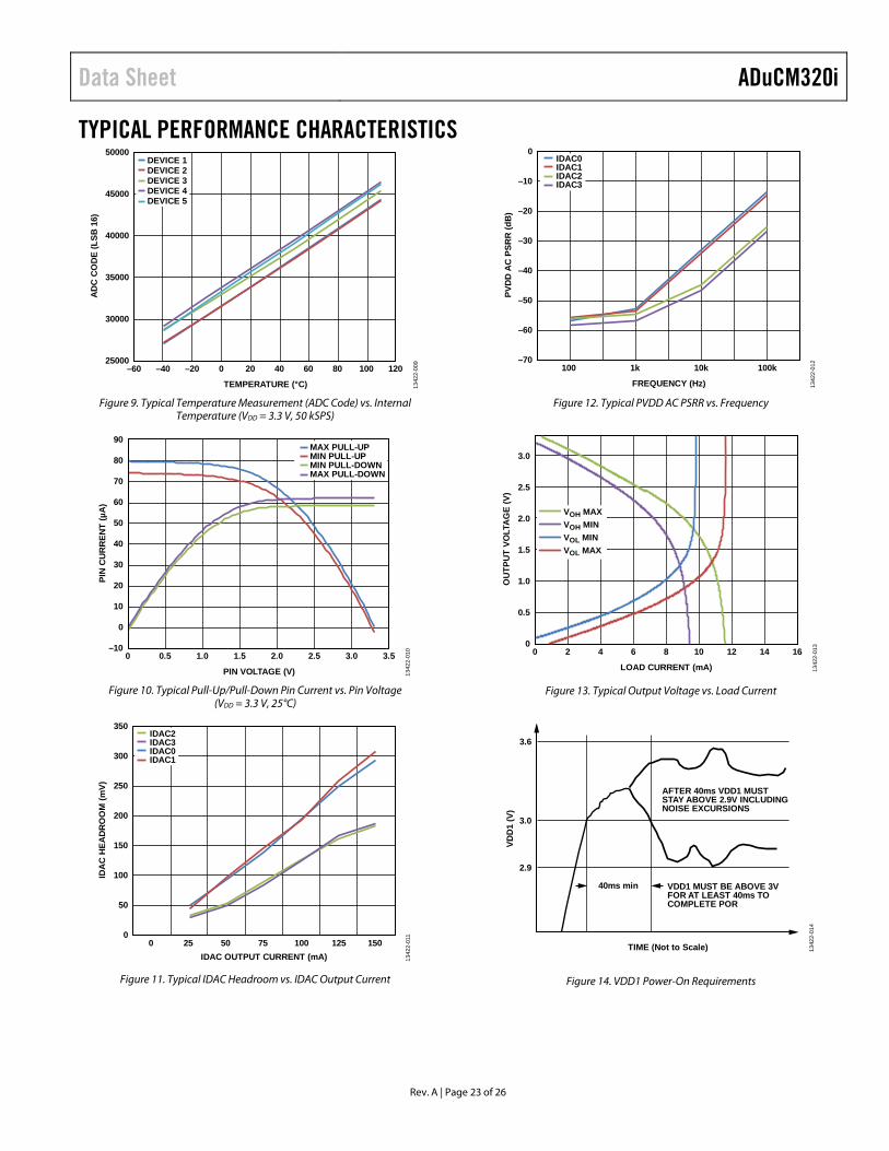
TEMPERATURE SENSOR Indicates die temperature, see Figure 9
Resolution 0.5 °C When precision calibrated by the user6
Accuracy1 1.34 1.43 V ADC measured voltage for temperature sensor channel without calibration, TA = 25°C
POWER-ON RESET POR 2.85 2.9 V PIN RESET
Minimum Time To Reset 1.2 µs Maximum Time Not To Reset 0.5 µs
WATCHDOG TIMER WDT Timeout Period 32 sec Default at power-up
FLASH/EE MEMORY Endurance1 10,000 Cycles Data Retention1 20 Years TJ = 85°C
DIGITAL INPUTS Input Leakage Current
Logic 1 GPIO 1 nA VIH = IOVDD, pull-up resistor disabled
Logic 0 GPIO 10 nA VIL = 0 V, pull-up resistor disabled
PRTADDRx, MCK 1 µA Pull-up disabled 16 µA Pull-up to 1.8 V enabled
Input Capacitance 10 pF MCK, PRTADDRx 6.5 pF MDIO 8.5 pF XTALI 5 pF XTALO 5 pF All Other Pins 10 pF
LOGIC INPUTS GPIO Input Voltage
Low VINL 0.25 × IOVDDx V High VINH 0.58 × IOVDDx V
MDIO PRTADDRx Input Voltage
Low VINL 0.36 V High VINH 0.84 V
MCK, MDIO Input Voltage Setup time ≥10 ns; hold time ≥10 ns; MCK/MDIO
Low VINL 0.36 V High VINH 0.84 V
Data Sheet ADuCM320i
Rev. A | Page 9 of 26
Parameter Symbol Min Typ Max Unit Test Conditions/Comments XTALI Input Voltage
Low VINL 1.1 V High VINH 1.7 V
Pull-Up Current 30 120 µA VIN = 0 V, see Figure 10 Pull-Down Current 30 100 µA VIN = 3.3 V, see Figure 10
LOGIC OUTPUTS All digital outputs excluding XTALO
GPIO Output Voltage7 High VOH IOVDDx − 0.4 V ISOURCE = 2 mA Low VOL 0.4 V ISINK = 2 mA
GPIO Short-Circuit Current1 11 mA See Figure 13 MDIO
Output Voltage High VOH 1.0 V ISOURCE = 4 mA Low VOL 0.2 V ISINK = 4 mA
Delay Time 100 ns MCK to MDIO out
OSCILLATORS Internal System Oscillator 16 MHz
Accuracy ±0.5 ±3 % System PLL 80 MHz Main system clock
External Crystal Oscillator 16 MHz Can be selected in place of internal oscillator
32 kHz Internal Oscillator 32.768 kHz Use for watchdog Accuracy ±5 ±20 %
External Clock 0.05 80 MHz Can be selected in place of PLL START-UP TIME Processor clock = 80 MHz
At Power-On 40 ms POR to first user code execution After Other Reset 1.5 ms Reset to first user code
execution From All Power-Down Modes 1.25 µs
PROGRAMMABLE LOGIC ARRAY PLA Propagation Delay
Pin 17 ns From input pin to output pin Element 1.5 ns Per PLA cell
EXTERNAL INTERRUPTS Pulse Width1
Level Triggered 7 ns Edge Triggered 1 ns
POWER REQUIREMENTS8 Power Supply Voltage Range
AVDDx to AGNDx and IOVDDx to DGNDx1
2.9 3.3 3.6 V
Analog Power Supply Currents AVDDx Current 6.3 mA Analog peripherals in idle mode
Digital Power Supply Current IOVDDx Current in Normal Mode 4 mA All GPIO pull-up resistors
enabled
ADuCM320i Data Sheet
Rev. A | Page 10 of 26
Parameter Symbol Min Typ Max Unit Test Conditions/Comments VDDx Current
Normal Mode 29 mA CD = 0 (80 MHz clock) executing typical code
20 mA CD = 1 executing typical code 10 mA CD = 7 executing typical code
CORE_SLEEP Mode 16 mA SYS_SLEEP Mode 8 mA Hibernate Mode 6.6 mA
Additional Power Supply Currents ADC 4.1 mA Continuously converting at
100 kSPS ADC Input Buffer 4.0 mA Both buffers enabled IDAC 16.5 mA Excluding load current DAC 340 µA Per powered up DAC,
excluding load current Total Supply Current 35 40 45 mA VDD1, IOVDDx, AVDDx
connected together; condition when entering user code: peripheral clocks on, peripherals idle, no load currents
Thermal Performance Impedance, Junction to Ambient 45 °C/W JEDEC 2S2P
1 These numbers are not production tested but are guaranteed by design and/or characterization data at production release. 2 Enabling the input buffer changes the ADC input characteristics as described in these specifications (the ADC Input Buffer specifications). 3 The data in the Microcontroller Electrical Specifications section also applies for a load of RL = 1 kΩ and CL = 100 pF to ground but only for 0 V to 2.5 V. However, this is
not production tested. 4 DAC linearity is calculated using a reduced code range of 100 to 3900. 5 DAC gain error is calculated using a reduced code range of 100 to an internal 2.5 V VREF. 6 Due to self heating, internal temperature measurements cannot be used to predict external temperatures. This value is only relevant after user calibration and only for
internal and external conditions identical to those at calibration. 7 The average current from all GPIO pins must not exceed 3 mA per pin. 8 Power specifications exclude any load currents to external circuits.

Data Sheet ADuCM320i
Rev. A | Page 11 of 26
TIMING SPECIFICATIONS I2C Timing
Table 2. I2C Timing in Standard Mode (100 kHz) Slave Parameter Description Min Typ Max Unit tL SCL low pulse width 4.7 µs tH SCL high pulse width 4.0 ns tSHD Start condition hold time 4.0 µs tDSU Data setup time 250 ns tDHD Data hold time (SDA held internally for 300 ns after falling edge of SCL) 0 3.45 µs tRSU Setup time for repeated start 4.7 µs tPSU Stop condition setup time 4.0 µs tBUF Bus-free time between a stop condition and a start condition 4.7 µs tR Rise time for both SCL and SDA 1 µs tF Fall time for both SCL and SDA 15 300 ns tVD; DAT Data valid time 3.45 µs tVD;ACK Data valid acknowledge time 3.45 µs
Table 3. I2C Timing in Fast Mode (400 kHz) Slave Parameter Description Min Typ Max Unit tL SCL low pulse width 1.3 µs tH SCL high pulse width 0.6 ns tSHD Start condition hold time 0.6 µs tDSU Data setup time 100 ns tDHD Data hold time (SDA held internally for 300 ns after falling edge of SCL) 0 µs tRSU Setup time for repeated start 0.6 µs tPSU Stop condition setup time 0.6 µs tBUF Bus-free time between a stop condition and a start condition 1.3 µs tR Rise time for both SCL and SDA 20 300 ns tF Fall time for both SCL and SDA 15 300 ns tVD; DAT Data valid time 0.9 µs tVD; ACK Data valid acknowledge time 0.9 µs
SDA (I/O) MSB LSB ACK MSB
1982–71SCL (I)
P SSTART
CONDITIONREPEATED
STARTSTOP
CONDITION
S(R)
tDSU
tH
tL
tSHD
tPSU
tDSU
tBUF
tDHD
tVD; DAT
tVD; ACK
tR
tF
tF
tR
tDHD
tRSU
1342
2-00
2
Figure 2. I2C-Compatible Interface Timing
ADuCM320i Data Sheet
Rev. A | Page 12 of 26
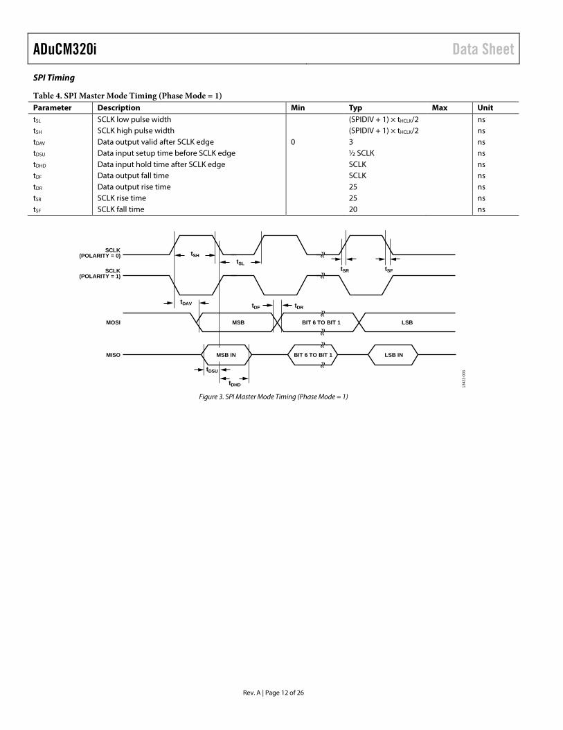
SPI Timing
Table 4. SPI Master Mode Timing (Phase Mode = 1) Parameter Description Min Typ Max Unit tSL SCLK low pulse width (SPIDIV + 1) × tHCLK/2 ns tSH SCLK high pulse width (SPIDIV + 1) × tHCLK/2 ns tDAV Data output valid after SCLK edge 0 3 ns tDSU Data input setup time before SCLK edge ½ SCLK ns tDHD Data input hold time after SCLK edge SCLK ns tDF Data output fall time SCLK ns tDR Data output rise time 25 ns tSR SCLK rise time 25 ns tSF SCLK fall time 20 ns
SCLK(POLARITY = 0)
SCLK(POLARITY = 1)
MOSI MSB BIT 6 TO BIT 1 LSB
MISO MSB IN BIT 6 TO BIT 1 LSB IN
tSHtSL
tSR tSF
tDRtDFtDAV
tDSU
tDHD 1342
2-00
3
Figure 3. SPI Master Mode Timing (Phase Mode = 1)
Data Sheet ADuCM320i
Rev. A | Page 13 of 26
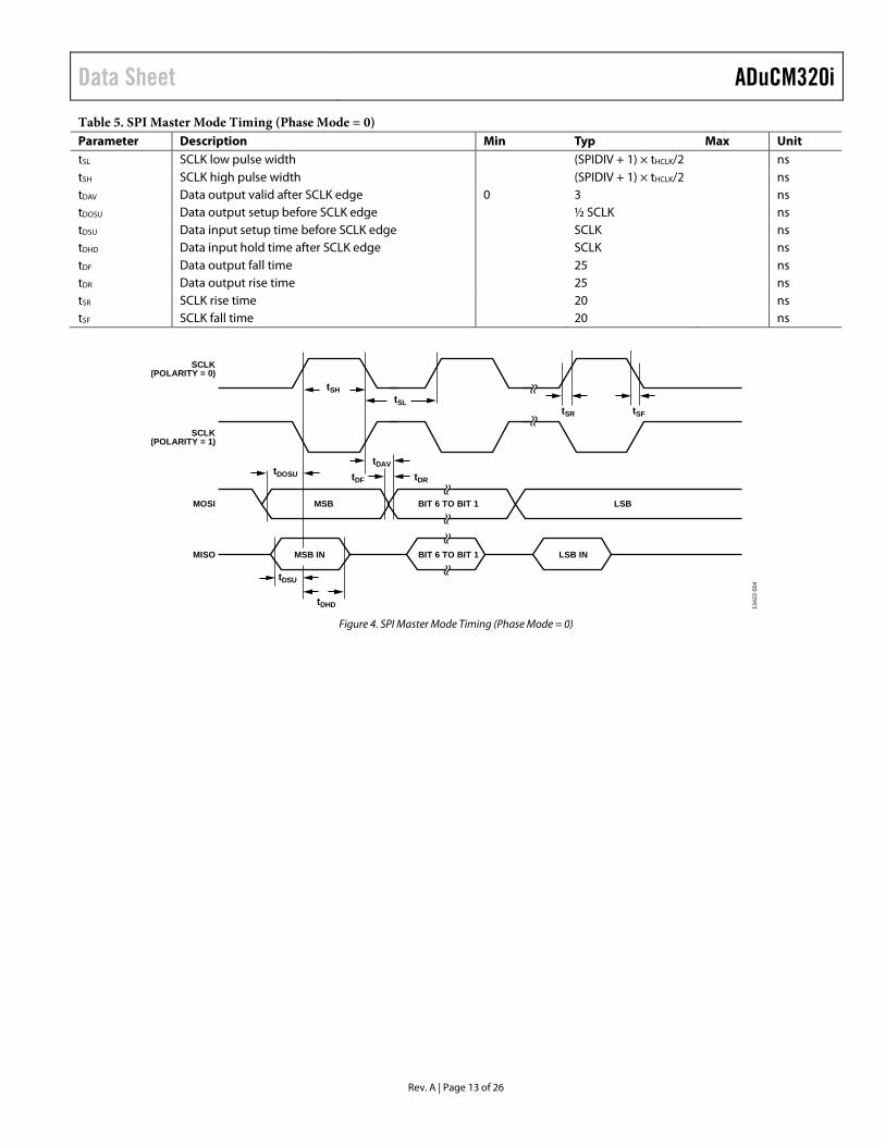
Table 5. SPI Master Mode Timing (Phase Mode = 0) Parameter Description Min Typ Max Unit tSL SCLK low pulse width (SPIDIV + 1) × tHCLK/2 ns tSH SCLK high pulse width (SPIDIV + 1) × tHCLK/2 ns tDAV Data output valid after SCLK edge 0 3 ns tDOSU Data output setup before SCLK edge ½ SCLK ns tDSU Data input setup time before SCLK edge SCLK ns tDHD Data input hold time after SCLK edge SCLK ns tDF Data output fall time 25 ns tDR Data output rise time 25 ns tSR SCLK rise time 20 ns tSF SCLK fall time 20 ns
SCLK(POLARITY = 0)
SCLK(POLARITY = 1)
tSHtSL
tSR tSF
MOSI MSB BIT 6 TO BIT 1 LSB
MISO MSB IN BIT 6 TO BIT 1 LSB IN
tDRtDF
tDAVtDOSU
tDSU
tDHD 1342
2-00
4
Figure 4. SPI Master Mode Timing (Phase Mode = 0)
ADuCM320i Data Sheet
Rev. A | Page 14 of 26
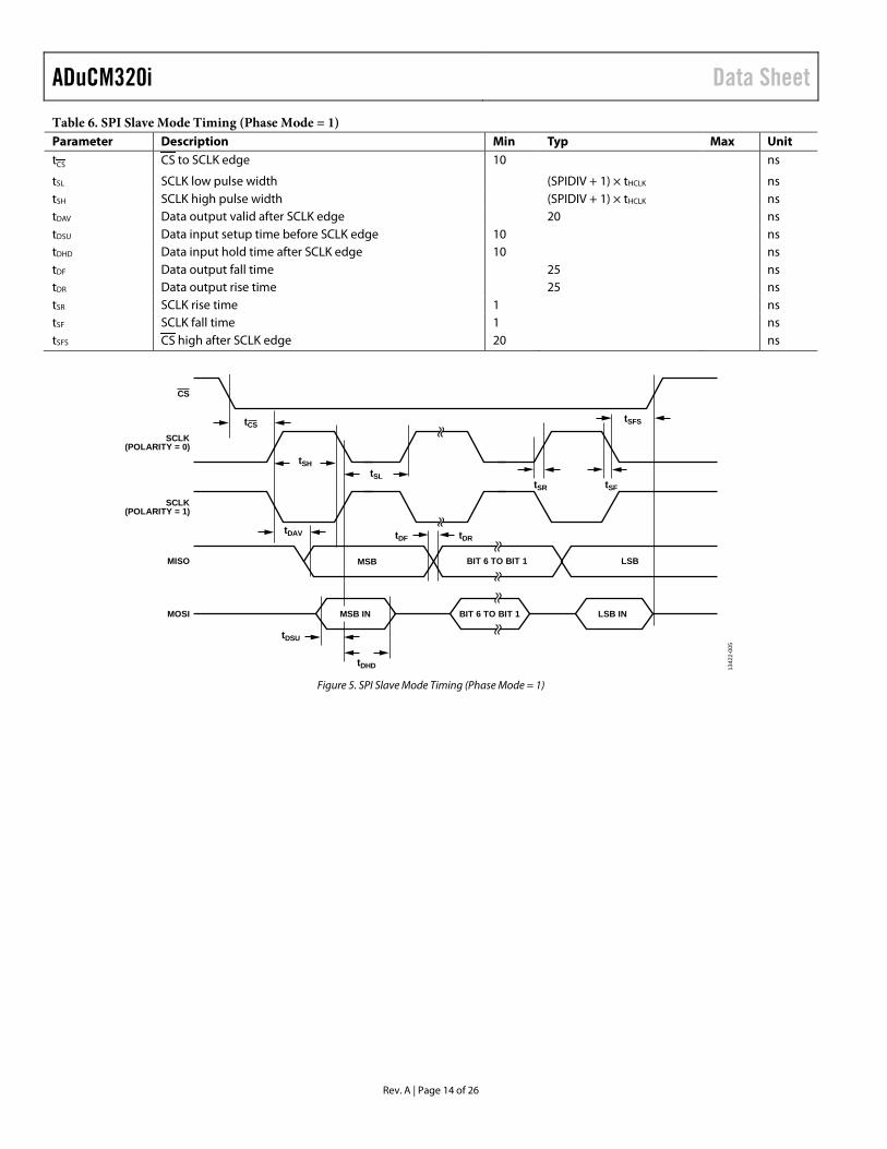
Table 6. SPI Slave Mode Timing (Phase Mode = 1) Parameter Description Min Typ Max Unit tCS CS to SCLK edge 10 ns
tSL SCLK low pulse width (SPIDIV + 1) × tHCLK ns tSH SCLK high pulse width (SPIDIV + 1) × tHCLK ns tDAV Data output valid after SCLK edge 20 ns tDSU Data input setup time before SCLK edge 10 ns tDHD Data input hold time after SCLK edge 10 ns tDF Data output fall time 25 ns tDR Data output rise time 25 ns tSR SCLK rise time 1 ns tSF SCLK fall time 1 ns tSFS CS high after SCLK edge 20 ns
SCLK(POLARITY = 0)
CS
SCLK(POLARITY = 1)
tSHtSL
tSR tSF
tSFS
MISO MSB BIT 6 TO BIT 1 LSB
MOSI MSB IN BIT 6 TO BIT 1 LSB IN
tDHD
tDSU
tDAV tDRtDF
tCS
1342
2-00
5
Figure 5. SPI Slave Mode Timing (Phase Mode = 1)
Data Sheet ADuCM320i
Rev. A | Page 15 of 26
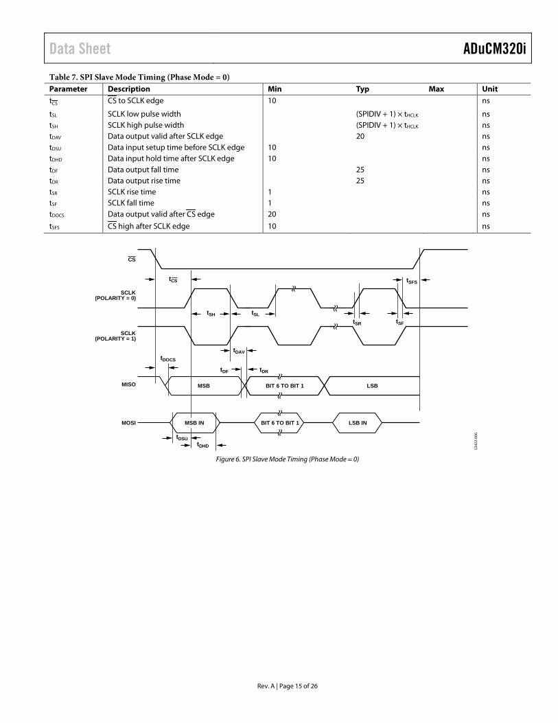
Table 7. SPI Slave Mode Timing (Phase Mode = 0) Parameter Description Min Typ Max Unit tCS CS to SCLK edge 10 ns
tSL SCLK low pulse width (SPIDIV + 1) × tHCLK ns tSH SCLK high pulse width (SPIDIV + 1) × tHCLK ns tDAV Data output valid after SCLK edge 20 ns tDSU Data input setup time before SCLK edge 10 ns tDHD Data input hold time after SCLK edge 10 ns tDF Data output fall time 25 ns tDR Data output rise time 25 ns tSR SCLK rise time 1 ns tSF SCLK fall time 1 ns tDOCS Data output valid after CS edge 20 ns
tSFS CS high after SCLK edge 10 ns
SCLK(POLARITY = 0)
CS
SCLK(POLARITY = 1)
tSH tSLtSR tSF
tSFS
MISO
MOSI MSB IN BIT 6 TO BIT 1 LSB IN
tDHD
tDSU
MSB BIT 6 TO BIT 1 LSB
tDOCS
tDAV
tDRtDF
tCS
1342
2-00
6
Figure 6. SPI Slave Mode Timing (Phase Mode = 0)
ADuCM320i Data Sheet
Rev. A | Page 16 of 26
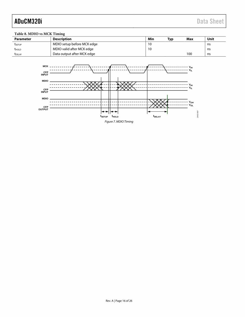
Table 8. MDIO vs MCK Timing Parameter Description Min Typ Max Unit tSETUP MDIO setup before MCK edge 10 ns tHOLD MDIO valid after MCK edge 10 ns tDELAY Data output after MCK edge 100 ns
MCK VIH
VIL
VIHVIL
VOHVOL
CFPINPUT
MDIO
CFPINPUT
MDIO
CFPOUTPUT
tSETUP tHOLD tDELAY 1342
2-00
7
Figure 7. MDIO Timing
Data Sheet ADuCM320i
Rev. A | Page 17 of 26
ABSOLUTE MAXIMUM RATINGS All requirements applicable to each pin must be met. Where multiple limits apply to a pin each one must be met individually. The limits apply according to the functionality of the pins at the time. Pins that can be either analog or digital, that is, that have two types indicated in the pin descriptions, must meet the limits for both types. For pin types, see Table 10.
When powered up, all ground pins and ADC_REFN must be connected together to a node referred to as GND in Table 9. The limits that are listed must be reduced by any difference between any GNDx pin. Also, AVDD3 must be connected to AVDD4 and IOVDD1 must be connected to IOVDD3.
Table 9. Parameter Rating Any Pin to GND −0.3 V to +3.9 V Any PVDDx Pin to GND −0.3 V to +2.8 V MDIO1, MCK, and PRTADDR0 to
PRTADDR4 in MDIO Mode to GND −0.3 V to +2.1 V
Between Any of AVDDx, IOVDDx, and VDD1 Pins
−0.3 V to +0.3 V
Any Type I Pin to GND2 −0.3 V to IOVDDx + 0.3 V Any Type AI or AO Pin to GND3 −0.3 V to AVDDx + 0.3 V Any IDACx, CDAMPx, IDAC_TST, IREF to
GND −0.3 V to PVDDx + 0.3 V
ADC_REFP to GND −0.3 V to AVDDx + 0.3 V Total Positive GPIO Pin Currents 0 mA to 30 mA Total Negative GPIO Pin Currents −30 mA to 0 mA Maximum Power Dissipation 1 W Operating Ambient Temperature Range −40°C to +105°C Storage Temperature Range −65°C to +160°C Operating Junction Temperature Range −40°C to +150°C ESD HBM 4 kV ESD FICDM 1 kV 1 Note that this pin is always in MDIO mode. 2 This limit does not apply if no current can be drawn by external circuits on
IOVDDx because, in this case, IOVDD follows to a suitable level. 3 This limit does not apply if no current can be drawn by external circuits on
AVDDx because, in this case, AVDD follows to a suitable level.
Stresses at or above those listed under Absolute Maximum Ratings may cause permanent damage to the product. This is a stress rating only; functional operation of the product at these or any other conditions above those indicated in the operational section of this specification is not implied. Operation beyond the maximum operating conditions for extended periods may affect product reliability.
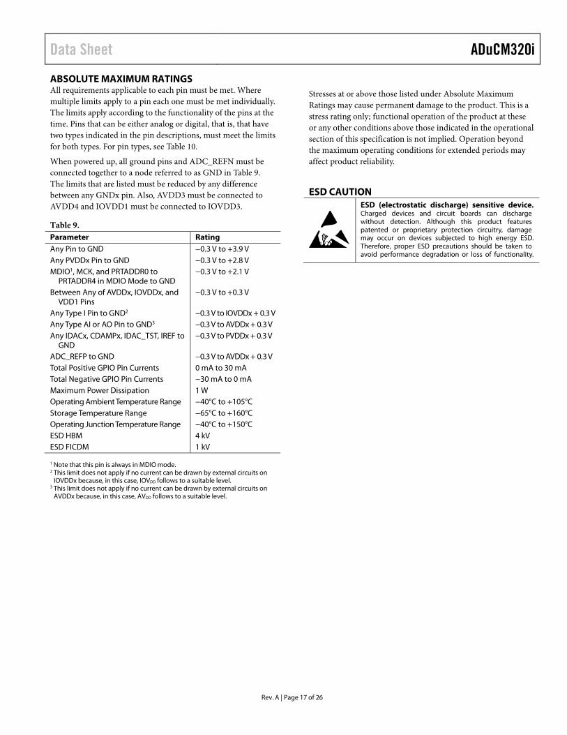
ESD CAUTION
ADuCM320i Data Sheet
Rev. A | Page 18 of 26
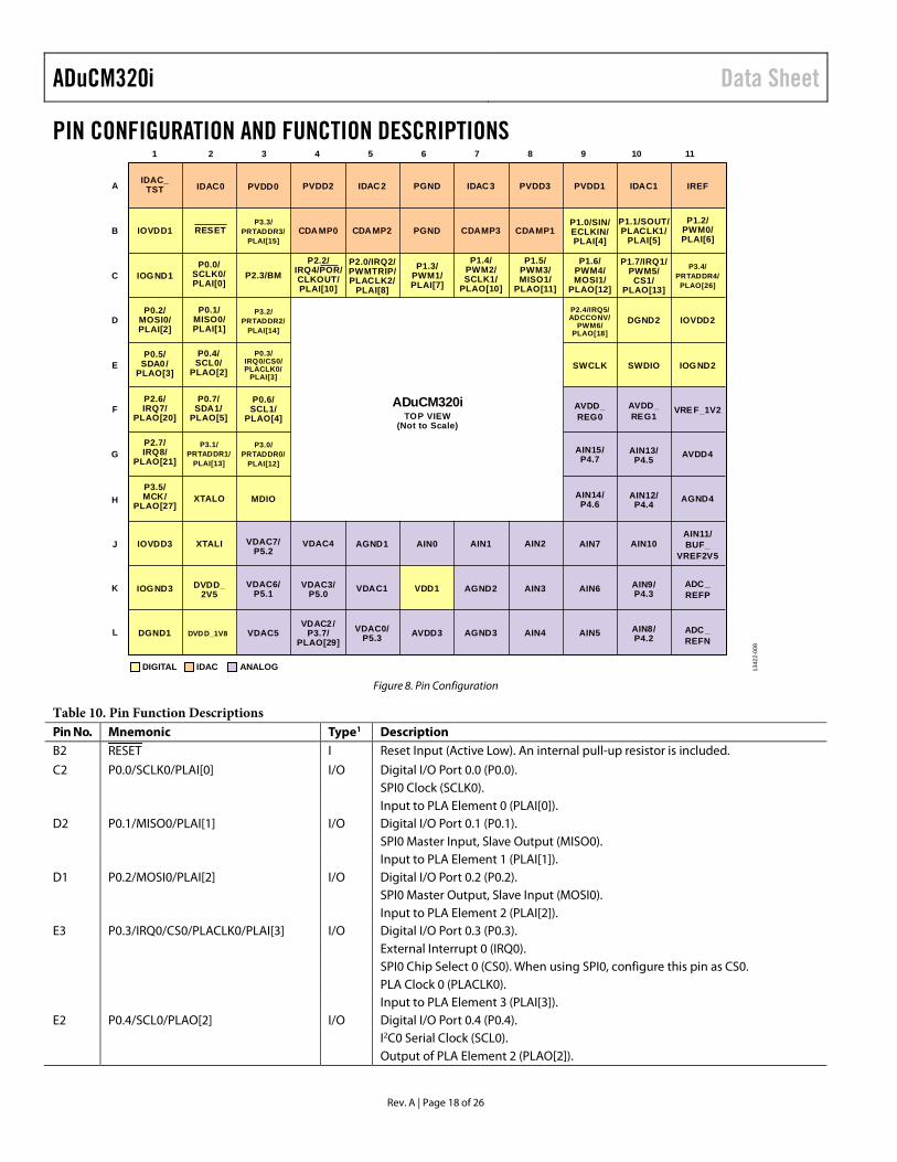
PIN CONFIGURATION AND FUNCTION DESCRIPTIONS 1
A
B
C
D
E
F
G
H
J
K
L
2 3 4 5 6 7 8 9 10 11
IDAC_TST IDAC0 IDAC 2
IOVDD1
DIGITAL
IOGND1
P3.3/PRTADDR3/
PLAI[15]
P0.0/SCLK0/PLAI[0]
CDA MP0 CDA MP2 CDAMP3 CDAMP1
IDAC1 IREFIDAC 3PGND
DGND2
SWCLK
AIN15/P4.7
AIN14/P4.6
AIN12/P4.4
AIN11/BUF_
VREF2V5AIN10AIN7AIN2AIN1AIN0AGND1VDAC4VDAC7/
P5.2
VDAC6/P5.1
XTALIIOVDD3
IOGND3 VDAC3/P5.0 VDAC1 VDD1
AVDD3
AGND2
AGND3
AIN3
AIN4
AIN6
AIN5
AIN9/P4.3
AIN8/P4.2
VDAC0/P5.3
VDAC2/P3.7/
PLAO[29]VDAC5DGND1
AGND4
AIN13/P4.5 AVDD4
SWDIO IOGND2
IOVDD2
PGND
PVDD0 1DDVP3DDVP2DDVP
RESETP1.0/SIN/ECLKIN/PLAI[4]
P1.2/PWM0/PLAI[6]
P1.1/SOUT/PLACLK1/
PLAI[5]
P2.4/IRQ5/ADCCONV/
PWM6/PLAO[18]
P1.3/PWM1/PLAI[7]
P1.4/PWM2/SCLK1/
PLAO[10]
P1.5/PWM3/MISO1/
PLAO[11]
P1.6/PWM4/MOSI1/
PLAO[12]
P1.7/IRQ1/PWM5/
CS1/PLAO[13]
P2.0/IRQ2/PWMTRIP/PLACLK2/
PLAI[8]
P2.2/IRQ4/POR/CLKOUT/PLAI[10]
P2.3/BM
P0.2/MOSI0/PLAI[2]
P0.5/SDA0/
PLAO[3]
P2.6/IRQ7/
PLAO[20]
P0.7/SDA1/
PLAO[5]
P0.6/SCL1/
PLAO[4]
P3.0/PRTADDR0/
PLAI[12]
P3.1/PRTADDR1/
PLAI[13]
P2.7/IRQ8/
PLAO[21]
P3.5/MCK/
PLAO[27]XTALO MDIO
P0.4/SCL0/
PLAO[2]
P0.3/IRQ0/CS0/PLACLK0/
PLAI[3]
P0.1/MISO0/PLAI[1]
P3.2/PRTADDR2/
PLAI[14]
P3.4/PRTADDR4/
PLAO[26]
AVDD_REG0
AVDD_REG1
VRE F_1V2
ADC _REFP
ADC _REFN
DVDD_2V5
DVDD_1V8
ADuCM320iTOP VIEW
(Not to Scale)
IDAC ANALOG 1342
2-00
8
Figure 8. Pin Configuration
Table 10. Pin Function Descriptions Pin No. Mnemonic Type1 Description B2 RESET I Reset Input (Active Low). An internal pull-up resistor is included.
C2 P0.0/SCLK0/PLAI[0] I/O Digital I/O Port 0.0 (P0.0). SPI0 Clock (SCLK0). Input to PLA Element 0 (PLAI[0]). D2 P0.1/MISO0/PLAI[1] I/O Digital I/O Port 0.1 (P0.1). SPI0 Master Input, Slave Output (MISO0). Input to PLA Element 1 (PLAI[1]). D1 P0.2/MOSI0/PLAI[2] I/O Digital I/O Port 0.2 (P0.2). SPI0 Master Output, Slave Input (MOSI0). Input to PLA Element 2 (PLAI[2]). E3 P0.3/IRQ0/CS0/PLACLK0/PLAI[3] I/O Digital I/O Port 0.3 (P0.3). External Interrupt 0 (IRQ0). SPI0 Chip Select 0 (CS0). When using SPI0, configure this pin as CS0. PLA Clock 0 (PLACLK0). Input to PLA Element 3 (PLAI[3]). E2 P0.4/SCL0/PLAO[2] I/O Digital I/O Port 0.4 (P0.4). I2C0 Serial Clock (SCL0). Output of PLA Element 2 (PLAO[2]).

Data Sheet ADuCM320i
Rev. A | Page 19 of 26
Pin No. Mnemonic Type1 Description E1 P0.5/SDA0/PLAO[3] I/O Digital I/O Port 0.5 (P0.5). I2C0 Serial Data (SDA0). Output of PLA Element 3 (PLAO[3]). F3 P0.6/SCL1/PLAO[4] I/O Digital I/O Port 0.6 (P0.6). I2C1 Serial Clock (SCL1). Output of PLA Element 4 (PLAO[4]). F2 P0.7/SDA1/PLAO[5] I/O Digital I/O Port 0.7 (P0.7). I2C1 Serial Data (SDA1). Output of PLA Element 5 (PLAO[5]). B9 P1.0/SIN/ECLKIN/PLAI[4] I/O Digital I/O Port 1.0 (P1.0). UART Input (SIN). External Input Clock (ECLKIN). Input to PLA Element 4 (PLAI[4]). B10 P1.1/SOUT/PLACLK1/PLAI[5] I/O Digital I/O Port 1.1 (P1.1). UART Output (SOUT) PLA Clock 1(PLACLK1). Input to PLA Element 5 (PLAI[5]). B11 P1.2/PWM0/PLAI[6] I/O Digital I/O Port 1.2 (P1.2). PWM Output 0 (PWM0). Input to PLA Element 6 (PLAI[6]). C6 P1.3/PWM1/PLAI[7] I/O Digital I/O Port 1.3 (P1.3). PWM Output 1 (PWM1). Input to PLA Element 7 (PLAI[7]). C7 P1.4/PWM2/SCLK1/PLAO[10] I/O Digital I/O Port 1.4 (P1.4). PWM Output 2 (PWM2). SPI1 Clock (SCLK1). Output of PLA Element 10 (PLAO[10]). C8 P1.5/PWM3/MISO1/PLAO[11] I/O Digital I/O Port 1.5 (P1.5). PWM Output 3 (PWM3). SPI1 Master Input, Slave Output (MISO1). Output of PLA Element 11 (PLAO[11]). C9 P1.6/PWM4/MOSI1/PLAO[12] I/O Digital I/O Port 1.6 (P1.6). PWM Output 4 (PWM4). SPI1 Master Output, Slave Input (MOSI1). Output of PLA Element 12 (PLAO[12]). C10 P1.7/IRQ1/PWM5/CS1/PLAO[13] I/O Digital I/O Port 1.7 (P1.7). External Interrupt 1 (IRQ1). PWM Output 5 (PWM5). SPI1 Chip Select 1 (CS1). When using SPI1, configure this pin as CS1. Output of PLA Element 13 (PLAO[13]). C5 P2.0/IRQ2/PWMTRIP/PLACLK2/PLAI[8] I/O Digital I/O Port 2.0 (P2.0). External Interrupt 2 (IRQ2). PWM Trip (PWMTRIP). PLA Input Clock 2 (PLACLK2). Input to PLA Element 8 (PLAI[8]). C4 P2.2/IRQ4/POR/CLKOUT/PLAI[10] I/O Digital I/O Port 2.2 (P2.2).
External Interrupt 4 (IRQ4). Reset Output (POR).
Clock Output (CLKOUT). Input to PLA Element 10 (PLAI[10]).
ADuCM320i Data Sheet
Rev. A | Page 20 of 26
Pin No. Mnemonic Type1 Description C3 P2.3/BM I/O Digital I/O Port 2.3 (P2.3). Boot Mode (BM). This pin determines the start-up sequence after every reset.
Pull-up is enabled at power-up. D9 P2.4/IRQ5/ADCCONV/PWM6/PLAO[18] I/O Digital I/O Port 2.4 (P2.4). External Interrupt 5 (IRQ5). External Input to Start ADC Conversions (ADCCONV). PWM Output 6 (PWM6). Output of PLA Element 18 (PLAO[18]). F1 P2.6/IRQ7/PLAO[20] I/O Digital I/O Port 2.6 (P2.6). External Interrupt 7 (IRQ7). Output of PLA Element 20 (PLAO[20]). G1 P2.7/IRQ8/PLAO[21] I/O Digital I/O Port 2.7 (P2.7). External Interrupt 8 (IRQ8). Output of PLA Element 21 (PLAO[21]). G3 P3.0/PRTADDR0/PLAI[12] I/O Digital I/O Port 3.0 (P3.0). MDIO Port Address Bit 0 (PRTADDR0). See the digital inputs parameter in Table 1
for details. Input to PLA Element 12 (PLAI[12]). G2 P3.1/PRTADDR1/PLAI[13] I/O Digital I/O Port 3.1 (P3.1). MDIO Port Address Bit 1 (PRTADDR1). See the digital inputs parameter in Table 1
for details. Input to PLA Element 13 (PLAI[13]). D3 P3.2/PRTADDR2/PLAI[14] I/O Digital I/O Port 3.2 (P3.2). MDIO Port Address Bit 2 (PRTADDR2). See the digital inputs parameter in Table 1
for details. Input to PLA Element 14 (PLAI[14]). B3 P3.3/PRTADDR3/PLAI[15] I/O Digital I/O Port 3.3 (P3.3). MDIO Port Address Bit 3 (PRTADDR3). See the digital inputs parameter in Table 1
for details. Input of PLA Element 15 (PLAI[15]). C11 P3.4/PRTADDR4/PLAO[26] I/O Digital I/O Port 3.4 (P3.4). MDIO Port Address Bit 4 (PRTADDR4). See the digital inputs parameter in Table 1
for details. Output of PLA Element 26 (PLAO[26]). H1 P3.5/MCK/PLAO[27] I/O Digital I/O Port 3.5 (P3.5). MDIO Clock (MCK) See the digital inputs parameter in Table 1 for more details.
Output of PLA Element 27 (PLAO[27]). H3 MDIO I/O MDIO Data. E9 SWCLK I Serial Wire Debug Clock. E10 SWDIO I/O Serial Wire Bidirectional Data. F11 VREF_1V2 S 1.2 V Reference. This pin cannot be used to source current externally. Connect
VREF_1V2 to AGNDx via a 470 nF capacitor. A11 IREF AI IDAC Reference Current. This pin generates the reference current for the IDACs
and is set by an external resistor, REXT. Connect REXT from IREF to AGND4. J6 AIN0 AI Analog Input 0. J7 AIN1 AI Analog Input 1. J8 AIN2 AI Analog Input 2. K8 AIN3 AI Analog Input 3. L8 AIN4 AI Analog Input 4. L9 AIN5 AI Analog Input 5. AIN5 can be the negative input for the comparator. K9 AIN6 AI Analog Input 6. AIN6 is also the positive input for the comparator. J9 AIN7 AI Analog Input 7.
Data Sheet ADuCM320i
Rev. A | Page 21 of 26
Pin No. Mnemonic Type1 Description L10 AIN8/P4.2 AI/I/O Analog Input 8 (AIN8). Digital I/O Port 4.2 (P4.2). K10 AIN9/P4.3 AI/I/O Analog Input 9 (AIN9). Digital I/O Port 4.3 (P4.3). J10 AIN10 AI Analog Input 10. J11 AIN11/BUF_VREF2V5 AI/AO Analog Input 11 (AIN11). Buffered 2.5 V Bias (BUF_VREF2V5). The maximum load is 1.2 mA. Connect
BUF_VREF2V5 to AGNDx via a 100 nF capacitor. H10 AIN12/P4.4 AI/I/O Analog Input 12 (AIN12). Digital I/O Port 4.4 (P4.4). G10 AIN13/P4.5 AI/I/O Analog Input 13 (AIN13). Digital I/O Port 4.5 (P4.5). H9 AIN14/P4.6 AI/I/O Analog Input 14 (AIN14). Digital I/O Port 4.6 (P4.6). G9 AIN15/P4.7 AI/I/O Analog Input 15 (AIN15). Digital I/O Port 4.7 (P4.7). L5 VDAC0/P5.3 AO/I/O Voltage DAC0 Output (VDAC0). Digital I/O Port 5.3 (P5.3). K5 VDAC1 AO Voltage DAC1 Output. L4 VDAC2/P3.7/PLAO[29] AO/I/O Voltage DAC2 Output (VDAC2). Digital I/O Port 3.7 (P3.7). Output of PLA Element 29 (PLAO[29]). K4 VDAC3/P5.0 AO/I/O Voltage DAC3 Output (VDAC3). Digital I/O Port 5.0 (P5.0). J4 VDAC4 AO Voltage DAC4 Output (VDAC4). L3 VDAC5 AO Voltage DAC5 Output (VDAC5). K3 VDAC6/P5.1 AO/I/O Voltage DAC6 Output (VDAC6). Digital I/O Port 5.1 (P5.1). J3 VDAC7/P5.2 AO/I/O Voltage DAC7 Output (VDAC7). Digital I/O Port 5.2 (P5.2). A2 IDAC0 AO IDAC0. 0 mA to 150 mA full-scale output. A3 PVDD0 S Power for IDAC0. B4 CDAMP0 AI Damping Capacitor 0. Connect a damping capacitor from this pin to PVDD0. A10 IDAC1 AO IDAC1. 0 mA to 150 mA full-scale output. A9 PVDD1 S Power for IDAC1. B8 CDAMP1 AI Damping Capacitor 1. Connect a damping capacitor from this pin to PVDD1. A5 IDAC2 AO IDAC2. 0 mA to 150 mA full-scale output. A4 PVDD2 S Power for IDAC2. B5 CDAMP2 AI Damping Capacitor 2. Connect a damping capacitor from this pin to PVDD2. A7 IDAC3 AO IDAC3. 0 mA to 150 mA full-scale output. A8 PVDD3 S Power for IDAC3. B7 CDAMP3 AI Damping Capacitor 3. Connect a damping capacitor from this pin to PVDD3. B6 PGND S Power Supply Ground for IDACs. A6 PGND S Power Supply Ground for IDACs. A1 IDAC_TST AI/AO Pin for IDAC Test Purposes. Leave IDAC_TST unconnected. L2 DVDD_1V8 AO 1.8 V Digital Supply. A 470 nF capacitor to DGND1 must be connected to this
pin to stabilize the internal 1.8 V regulator that supplies flash memory and the Arm Cortex-M3 processor.
K2 DVDD_2V5 AO 2.5 V Digital Supply. A 470 nF capacitor to IOGND3 must be connected to this pin to stabilize the internal 2.5 V regulator that supplies the analog digital control.
ADuCM320i Data Sheet
Rev. A | Page 22 of 26
Pin No. Mnemonic Type1 Description F9 AVDD_REG0 AO Analog Regulator 0 Supply. A 470 nF capacitor to AGND4 must be connected to
this pin to stabilize the internal 2.5 V regulator that supplies the ADC. F10 AVDD_REG1 AO Analog Regulator 1 Supply. Output of 2.5 V on-chip LDO regulator. A 470 nF
capacitor to AGND4 must be connected to this pin. This regulator supplies the IDACs.
L1 DGND1 S Digital Ground 1 for DVDD_1V8. D10 DGND2 S Digital Ground 2. Connect to DGND1. B1 IOVDD1 S 3.3 V GPIO Supply. D11 IOVDD2 S 3.3 V GPIO Supply and Interdie Communications. J1 IOVDD3 S 3.3 V GPIO Supply. C1 IOGND1 S Ground for IOVDD1. E11 IOGND2 S Ground for IOVDD2. K1 IOGND3 S Ground for IOVDD3 and Interdie Communications. J5 AGND1 S Analog Ground for VDD1. K7 AGND2 S ESD Ground for Pad Ring. L7 AGND3 S Ground for AVDD3. H11 AGND4 S Ground for AVDD4, AVDD_REG0, and AVDD_REG1. K6 VDD1 S 3.3 V Supply for Digital Die. L6 AVDD3 S VDAC and IDAC Supply (3.3 V). G11 AVDD4 S ADC Supply (3.3 V). L11 ADC_REFN AO/A Negative Decoupling Capacitor Connection for ADC Reference Buffer. Connect
this pin to AGND4. K11 ADC_REFP AO/A Positive Decoupling Capacitor Connection for ADC Reference Buffer. Connect
this pin to a 4.7 µF capacitor to the ADC_REFN pin. ADC_REFP can be overdriven by an external reference.
H2 XTALO O Output from the Crystal Oscillator Inverter. When not using an external crystal, leave XTALO unconnected.
J2 XTALI I Input to the Crystal Oscillator Inverter and Input to the Internal Clock Generator Circuits. When not using an external crystal, connect XTALI to DGNDx.
1 I is digital input, O is digital output, S is supply, AI is analog input, and AO is analog output.
Data Sheet ADuCM320i
Rev. A | Page 23 of 26
TYPICAL PERFORMANCE CHARACTERISTICS
25000
30000
35000
40000
45000
50000
–60 –40 –20 0 20 40 60 80 100 120
AD
C C
OD
E (L
SB 1
6)
TEMPERATURE (°C)
DEVICE 1DEVICE 2DEVICE 3DEVICE 4DEVICE 5
1342
2-00
9
Figure 9. Typical Temperature Measurement (ADC Code) vs. Internal
Temperature (VDD = 3.3 V, 50 kSPS)
–10
0
10
20
30
40
50
60
70
80
90
0 0.5 1.0 1.5 2.0 2.5 3.0 3.5
PIN
CU
RR
ENT
(µA
)
PIN VOLTAGE (V)
MAX PULL-UPMIN PULL-UPMIN PULL-DOWNMAX PULL-DOWN
1342
2-01
0
Figure 10. Typical Pull-Up/Pull-Down Pin Current vs. Pin Voltage
(VDD = 3.3 V, 25°C)
0
50
100
150
200
250
300
350
0 25 50 75 100 125 150
IDA
C H
EAD
RO
OM
(mV)
IDAC OUTPUT CURRENT (mA)
IDAC2IDAC3IDAC0IDAC1
1342
2-01
1
Figure 11. Typical IDAC Headroom vs. IDAC Output Current
–70
–60
–50
–40
–30
–20
–10
0
100 1k 10k 100k
PVD
DA
C P
SRR
(dB
)
FREQUENCY (Hz)
IDAC0 IDAC1 IDAC2 IDAC3
1342
2-01
2
Figure 12. Typical PVDD AC PSRR vs. Frequency
0
0.5
1.0
1.5
2.0
2.5
3.0
2 6 10 14 160 4 8 12
OU
TPU
T VO
LTA
GE
(V)
LOAD CURRENT (mA)
VOH MAXVOH MINVOL MINVOL MAX
1342
2-01
3
Figure 13. Typical Output Voltage vs. Load Current
TIME (Not to Scale)
3.6
40ms min
VDD
1 (V
)
VDD1 MUST BE ABOVE 3VFOR AT LEAST 40ms TOCOMPLETE POR
AFTER 40ms VDD1 MUSTSTAY ABOVE 2.9V INCLUDINGNOISE EXCURSIONS
3.0
2.9
1342
2-01
4
Figure 14. VDD1 Power-On Requirements
ADuCM320i Data Sheet
Rev. A | Page 24 of 26
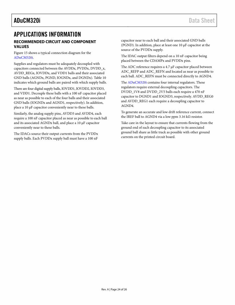
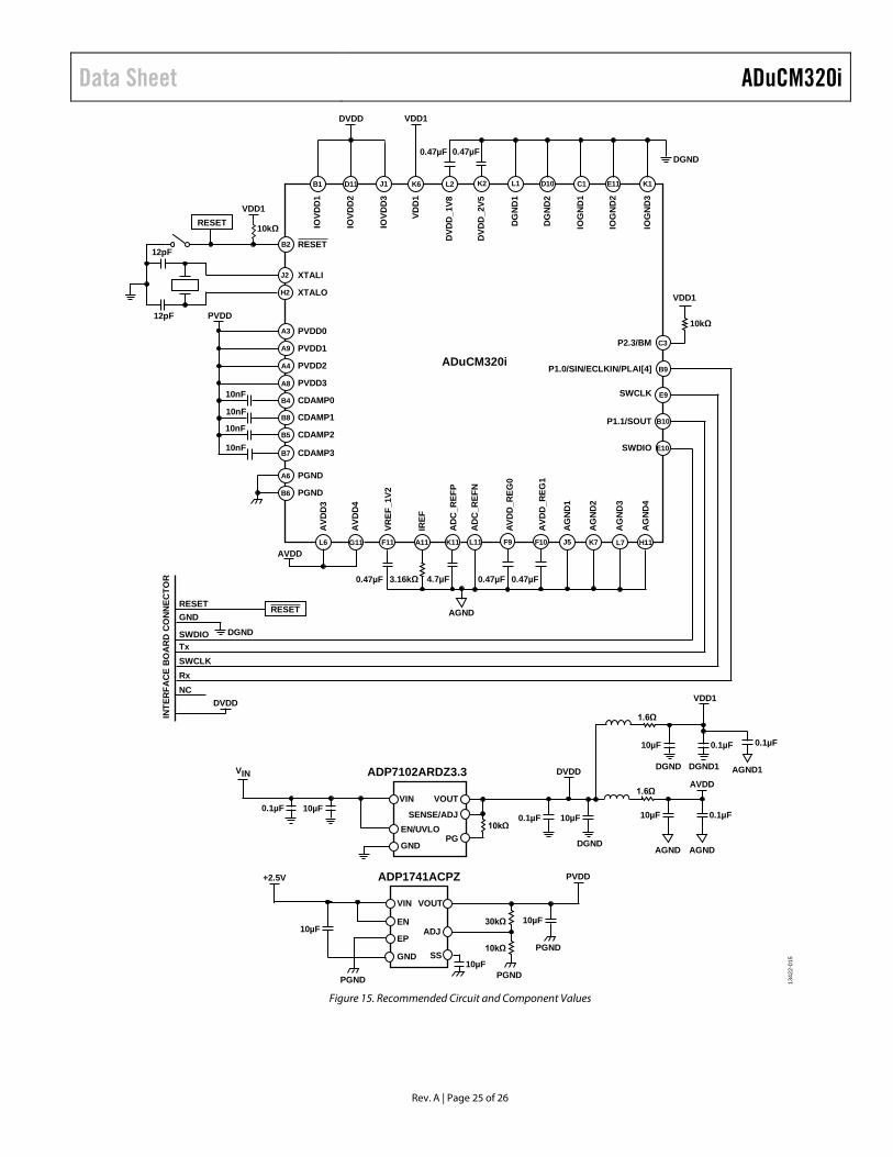
APPLICATIONS INFORMATION RECOMMENDED CIRCUIT AND COMPONENT VALUES Figure 15 shows a typical connection diagram for the ADuCM320i.
Supplies and regulators must be adequately decoupled with capacitors connected between the AVDDx, PVDDx, DVDD_x, AVDD_REGx, IOVDDx, and VDD1 balls and their associated GND balls (AGNDx, PGND, IOGNDx, and DGNDx). Table 10 indicates which ground balls are paired with which supply balls.
There are four digital supply balls, IOVDD1, IOVDD2, IOVDD3, and VDD1. Decouple these balls with a 100 nF capacitor placed as near as possible to each of the four balls and their associated GND balls (IOGNDx and AGND1, respectively). In addition, place a 10 μF capacitor conveniently near to these balls.
Similarly, the analog supply pins, AVDD3 and AVDD4, each require a 100 nF capacitor placed as near as possible to each ball and its associated AGNDx ball, and place a 10 μF capacitor conveniently near to these balls.
The IDACs source their output currents from the PVDDx supply balls. Each PVDDx supply ball must have a 100 nF
capacitor near to each ball and their associated GND balls (PGND). In addition, place at least one 10 μF capacitor at the source of the PVDDx supply.
The IDAC output filters depend on a 10 nF capacitor being placed between the CDAMPx and PVDDx pins.
The ADC reference requires a 4.7 μF capacitor placed between ADC_REFP and ADC_REFN and located as near as possible to each ball. ADC_REFN must be connected directly to AGND4.
The ADuCM320i contains four internal regulators. These regulators require external decoupling capacitors. The DVDD_1V8 and DVDD_2V5 balls each require a 470 nF capacitor to DGND1 and IOGND3, respectively. AVDD_REG0 and AVDD_REG1 each require a decoupling capacitor to AGND4.
To generate an accurate and low drift reference current, connect the IREF ball to AGND4 via a low ppm 3.16 kΩ resistor.
Take care in the layout to ensure that currents flowing from the ground end of each decoupling capacitor to its associated ground ball share as little track as possible with other ground currents on the printed circuit board.
Data Sheet ADuCM320i
Rev. A | Page 25 of 26
G11L6
B6 PGND
RESET RESET
AD
C_R
EFP
GNDDGNDSWDIO
TxSWCLK
AVDD
AVD
D3
AVD
D4
VREF
_1V2
IREF
AD
C_R
EFN
AVD
D_R
EG0
AVD
D_R
EG1
AG
ND
1
AG
ND
3
AG
ND
2
F9L11K11A11F11 H11L7K7J5F10
AG
ND
4
3.16kΩ0.47µF 4.7µF 0.47µF 0.47µF
B2
C1 E11
P1.1/SOUT
J2
SWDIO
H2
A3
A9
12pF
10nF
A6 PGND
L1 D10
ADuCM320i
CDAMP2
CDAMP1
CDAMP0
PVDD3
PVDD2
PVDD1
PVDD0
XTALO
XTALI
RESET
RESET
A4
A8
B4
B8
B5
VDD1
CDAMP3B7
SWCLK
P1.0/SIN/ECLKIN/PLAI[4]
P2.3/BM
K1
IOVD
D1
IOVD
D3
IOVD
D2
VD
D1
DVD
D_1
V8
DVD
D_2
V5
DG
ND
1
DG
ND
2
IOG
ND
1
IOG
ND
2
IOG
ND
3
10kΩ
PVDD
10nF
10nF
10nF
DVDD VDD1
0.47µF 0.47µF
VDD1
10kΩ
10µF10µF
0.1µF10kΩ
1.6ΩVIN VOUT
EN/UVLO
GND DGND
AVDDDVDD
AGND AGND
0.1µF 10µF
ADP7102ARDZ3.3
0.1µF
VIN
SENSE/ADJ
PG
0.1µF
1.6Ω
VDD1
DGND DGND1
10µF
VIN VOUT
EN
GND
ADP1741ACPZ
SS
EP
10µF30kΩ
10kΩ
10µF
+2.5V
10µF ADJ
PVDD
12pF
PGND
PGNDPGND
DGND
NCDVDD
AGND
0.1µF
AGND1
L2K6J1D11B1 K2
E10
B10
E9
B9
C3
INTE
RFA
CE
BO
AR
D C
ON
NEC
TOR
Rx
1342
2-01
5
Figure 15. Recommended Circuit and Component Values
ADuCM320i Data Sheet
Rev. A | Page 26 of 26
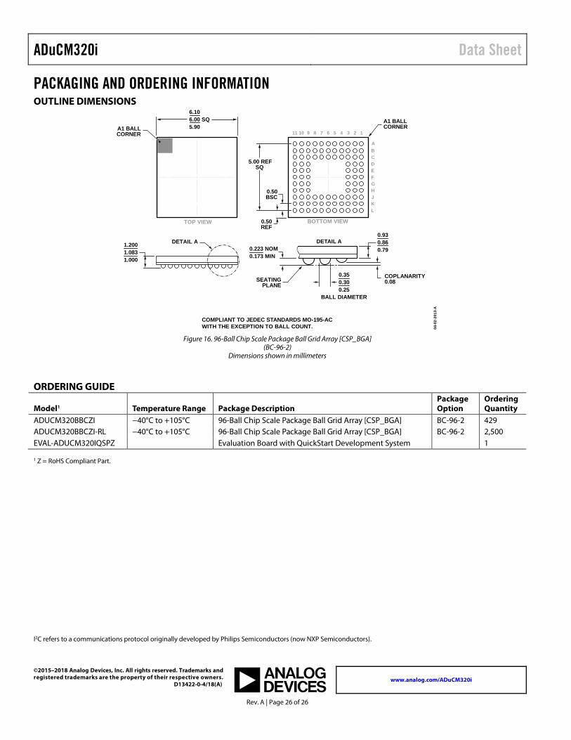
PACKAGING AND ORDERING INFORMATION OUTLINE DIMENSIONS
6.106.00 SQ5.90
5.00 REFSQ
0.350.300.25
04-0
2-20
13-A
COPLANARITY0.08
ABCDEFGHJKL
7 6 3 2 15 4
BALL DIAMETER
0.50BSC
0.50REF
DETAIL A
A1 BALLCORNERA1 BALL
CORNER
DETAIL A
BOTTOM VIEWTOP VIEW
SEATINGPLANE
1.2001.0831.000
891011
COMPLIANT TO JEDEC STANDARDS MO-195-ACWITH THE EXCEPTION TO BALL COUNT.
0.223 NOM0.173 MIN
0.930.860.79
Figure 16. 96-Ball Chip Scale Package Ball Grid Array [CSP_BGA]
(BC-96-2) Dimensions shown in millimeters
ORDERING GUIDE
Model1 Temperature Range Package Description Package Option
Ordering Quantity
ADUCM320BBCZI −40°C to +105°C 96-Ball Chip Scale Package Ball Grid Array [CSP_BGA] BC-96-2 429 ADUCM320BBCZI-RL −40°C to +105°C 96-Ball Chip Scale Package Ball Grid Array [CSP_BGA] BC-96-2 2,500 EVAL-ADUCM320IQSPZ Evaluation Board with QuickStart Development System 1 1 Z = RoHS Compliant Part.
I2C refers to a communications protocol originally developed by Philips Semiconductors (now NXP Semiconductors).
©2015–2018 Analog Devices, Inc. All rights reserved. Trademarks and registered trademarks are the property of their respective owners.
D13422-0-4/18(A)
www.analog.com/ADuCM320i