PP (ultiPil Photon ount aays - Hamamatsu Photonics · 1 S13361-3050 series PP aays in a chip si...
11
1 S13361-3050 series MPPC arrays in a chip size package miniaturized through the adoption of TSV structure MPPC ® (Multi-Pixel Photon Counter) arrays www.hamamatsu.com The S13361-3050 series is a MPPC array for precision measurement miniaturized by the use of TSV (through-silicon via) and CSP (chip size package) technologies. The adoption of a TSV structure made it possible to eliminate wiring on the photosensitive area side, resulting in a compact structure with little dead space compared with previous products. The four-side buttable structure allows multiple devices to be arranged side by side to fabricate large-area devices. They are suitable for applications, such as medical, non-destructive inspection, environmental analysis, and high energy physics experiment, that require photon counting measurement. Outstanding photon counting capability (outstanding photon detection efficiency versus numbers of incident photons) Low crosstalk Low afterpulses Low voltage (VBR=53 V typ.) operation High gain: 10 5 to 10 6 Compact chip size package with little dead space Features Astro physical application Nuclear medicine High energy physics experiment PET Environmental analysis Applications Pulse waveform comparison (typical example) Lower noise When an MPPC detects photons, the output may contain spurious pulses, namely afterpulse and crosstalk, that are separate from the out- put pulses of the incident photons. Afterpulses are output later than the timing at which the incident light is received. Crosstalk is output from other pixels at the same time as the detection of light. Previous products achieved lower afterpulse through the improvement of material and wafer process technology, but with the S13361-3050 series, low crosstalk has been achieved in addition to low afterpulse. (M=1.25 × 10 6 ) 10 ns 50 mV Previous product Improved product (reference data: S13360-3050VE) (M=1.25 × 10 6 ) 10 ns 50 mV
Transcript of PP (ultiPil Photon ount aays - Hamamatsu Photonics · 1 S13361-3050 series PP aays in a chip si...

1
S13361-3050 series
MPPC arrays in a chip size package miniaturized through the adoption of TSV structure
MPPC® (Multi-Pixel Photon Counter) arrays
www.hamamatsu.com
The S13361-3050 series is a MPPC array for precision measurement miniaturized by the use of TSV (through-silicon via) and CSP (chip size package) technologies. The adoption of a TSV structure made it possible to eliminate wiring on the photosensitive area side, resulting in a compact structure with little dead space compared with previous products. The four-side buttable structure allows multiple devices to be arranged side by side to fabricate large-area devices. They are suitable for applications, such as medical, non-destructive inspection, environmental analysis, and high energy physics experiment, that require photon counting measurement.
Outstanding photon counting capability (outstanding photon detection efficiency versus numbers of incident photons)
Low crosstalkLow afterpulses
Low voltage (VBR=53 V typ.) operationHigh gain: 105 to 106
Compact chip size package with little dead space
Features
Astro physical application
Nuclear medicineHigh energy physics experiment
PETEnvironmental analysis
Applications
Pulse waveform comparison (typical example)
Lower noise
When an MPPC detects photons, the output may contain spurious pulses, namely afterpulse and crosstalk, that are separate from the out-put pulses of the incident photons. Afterpulses are output later than the timing at which the incident light is received. Crosstalk is output from other pixels at the same time as the detection of light.Previous products achieved lower afterpulse through the improvement of material and wafer process technology, but with the S13361-3050 series, low crosstalk has been achieved in addition to low afterpulse.
(M=1.25 × 10⁶)
10 ns
50 m
V
Previous product Improved product (reference data: S13360-3050VE)(M=1.25 × 10⁶)
10 ns
50 m
V
2
MPPC (Multi-Pixel Photon Counter) arrays S13361-3050 series
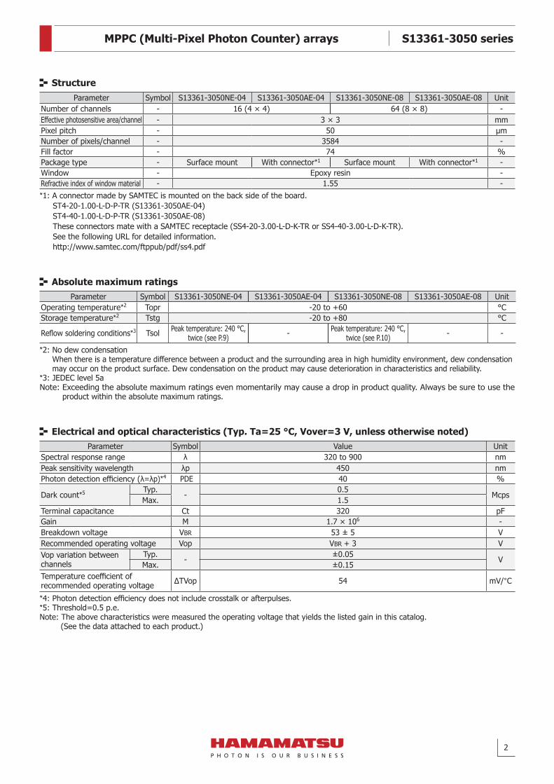
StructureParameter Symbol S13361-3050NE-04 S13361-3050AE-04 S13361-3050NE-08 S13361-3050AE-08 Unit
Number of channels - 16 (4 × 4) 64 (8 × 8) -Effective photosensitive area/channel - 3 × 3 mmPixel pitch - 50 µmNumber of pixels/channel - 3584 -Fill factor - 74 %Package type - Surface mount With connector*1 Surface mount With connector*1 -Window - Epoxy resin -Refractive index of window material - 1.55 -*1: A connector made by SAMTEC is mounted on the back side of the board.
ST4-20-1.00-L-D-P-TR (S13361-3050AE-04)ST4-40-1.00-L-D-P-TR (S13361-3050AE-08)These connectors mate with a SAMTEC receptacle (SS4-20-3.00-L-D-K-TR or SS4-40-3.00-L-D-K-TR).See the following URL for detailed information.http://www.samtec.com/ftppub/pdf/ss4.pdf
Electrical and optical characteristics (Typ. Ta=25 °C, Vover=3 V, unless otherwise noted)Parameter Symbol Value Unit
Spectral response range λ 320 to 900 nmPeak sensitivity wavelength λp 450 nmPhoton detection efficiency (λ=λp)*4 PDE 40 %
Dark count*5 Typ. - 0.5 McpsMax. 1.5Terminal capacitance Ct 320 pFGain M 1.7 × 10⁶ -Breakdown voltage VBR 53 ± 5 VRecommended operating voltage Vop VBR + 3 VVop variation between channels
Typ. - ±0.05 VMax. ±0.15Temperature coefficient of recommended operating voltage ΔTVop 54 mV/°C
*4: Photon detection efficiency does not include crosstalk or afterpulses.*5: Threshold=0.5 p.e.Note: The above characteristics were measured the operating voltage that yields the listed gain in this catalog.
(See the data attached to each product.)
Absolute maximum ratingsParameter Symbol S13361-3050NE-04 S13361-3050AE-04 S13361-3050NE-08 S13361-3050AE-08 Unit
Operating temperature*2 Topr -20 to +60 °CStorage temperature*2 Tstg -20 to +80 °C
Reflow soldering conditions*3 Tsol Peak temperature: 240 °C, twice (see P.9) - Peak temperature: 240 °C,
twice (see P.10) - -
*2: No dew condensation When there is a temperature difference between a product and the surrounding area in high humidity environment, dew condensation may occur on the product surface. Dew condensation on the product may cause deterioration in characteristics and reliability.
*3: JEDEC level 5aNote: Exceeding the absolute maximum ratings even momentarily may cause a drop in product quality. Always be sure to use the
product within the absolute maximum ratings.

3
MPPC (Multi-Pixel Photon Counter) arrays S13361-3050 series
Photon detection efficiency vs. wavelength (typical example)
Photon detection efficiency does not include crosstalk or afterpulses.
KAPDB0318EA
0
10
20
30
40
50
200 400300 500 600 700 800 1000900
Phot
on d
etec
tion
effic
ienc
y (%
)
Wavelength (nm)
(Ta=25 °C)
Photon detection efficiency vs. wavelength
KAPDB0318EA
Overvoltage specifications of gain, crosstalk probability, photon detection efficiency (typical example)
KAPDB0324EA
Photon detection efficiency vs. overvoltage
KAPDB0324EA
0 2 4 1086
6 × 10⁶
5 × 10⁶
3 × 10⁶
1 × 10⁶
4 × 10⁶
2 × 10⁶
0
60
40
50
30
20
10
0
Gain
Cros
stal
k pr
obab
ility,
pho
ton
dete
ctio
n ef
ficie
ncy
(%)
Overvoltage (V)
GainCrosstalk probabilityPhoton detection efficiency (λ=450 nm)
(Ta=25 °C)
MPPC characteristics vary with the operating voltage. Although increasing the operating voltage improves the photon detection effi-ciency and time resolution, it also increases the dark count and crosstalk at the same time, so an optimum operating voltage must be selected to match the application.
4
MPPC (Multi-Pixel Photon Counter) arrays S13361-3050 series
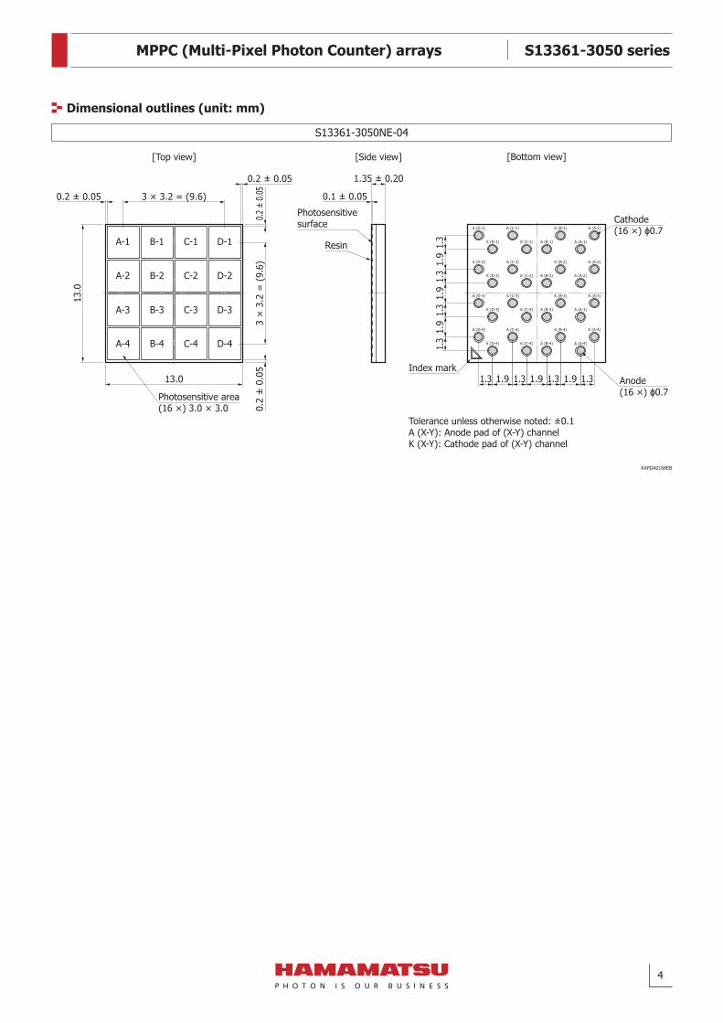
Dimensional outlines (unit: mm)Dimensional outline (unit: mm)
[Bottom view][Top view] [Side view]
Tolerance unless otherwise noted: ±0.1A (X-Y): Anode pad of (X-Y) channelK (X-Y): Cathode pad of (X-Y) channel
KAPDA0168EB
13.0
13.0
A-1
A-2
A-3
A-4
B-1
B-2
B-3
B-4
C-1
C-2
C-3
C-4
D-1
D-2
D-3
D-4
Photosensitive area(16 ×) 3.0 × 3.0
3 × 3.2 = (9.6)
0.2 ± 0.05
0.2 ± 0.05
3 ×
3.2
= (
9.6)
0.2
± 0
.05
0.2
± 0.
05
1.35 ± 0.20
0.1 ± 0.05
Resin
Photosensitive surface
1.9 1.3 1.9 1.3 1.9 1.31.3
Cathode(16 ×) ϕ0.7A (D-1)
K (D-1)
A (C-1)
K (C-1)
A (D-2)
K (D-2)
A (C-2)
K (C-2)
K (B-1)
A (B-1)
K (A-1)
A (A-1)
K (B-2)
A (B-2)
K (A-2)
A (A-2)
A (D-3)
K (D-3)
A (C-3)
K (C-3)
A (D-4)
K (D-4)
A (C-4)
K (C-4)
K (B-3)
A (B-3)
K (A-3)
A (A-3)
K (B-4)
A (B-4)
K (A-4)
A (A-4)
Anode(16 ×) ϕ0.7
Index mark
1.9
1.3
1.9
1.3
1.9
1.3
1.3
KAPDA0168EB
S13361-3050NE-04

5
MPPC (Multi-Pixel Photon Counter) arrays S13361-3050 seriesDimensional outline (unit: mm)
[Bottom view][Top view] [Side view]
Tolerance unless otherwise noted: ±0.1
KAPDA0169EB
13.0
13.0
A-1
A-2
A-3
A-4
B-1
B-2
B-3
B-4
C-1
C-2
C-3
C-4
D-1
D-2
D-3
D-4
1.35 ± 0.20
0.1 ± 0.05
Resin
Photosensitive surface
(3 ×) Index mark
(3.7)Connector (SAMTEC)ST4-20-1.00-L-D-P-TR
2019181716151413121110987654321
2122232425262728293031323334353637383940
(3.08)
(9.4
)
Photosensitive area(16 ×) 3.0 × 3.0
3 × 3.2 = (9.6)
0.2 ± 0.05
0.2 ± 0.05
3 ×
3.2
= (
9.6)
0.2
± 0
.05
0.2
± 0.
05
Pin no. Connection Pin no. Connection20 K (C-1) 21 K (B-1)19 K (D-1) 22 K (A-1)18 NC 23 NC17 A (C-1) 24 A (B-1)16 A (D-1) 25 A (A-1)15 A (D-2) 26 A (A-2)14 A (C-2) 27 A (B-2)13 NC 28 NC12 K (D-2) 29 K (A-2)11 K (C-2) 30 K (B-2)10 K (C-3) 31 K (B-3)9 K (D-3) 32 K (A-3)8 NC 33 NC7 A (C-3) 34 A (B-3)6 A (D-3) 35 A (A-3)5 A (D-4) 36 A (A-4)4 A (C-4) 37 A (B-4)3 NC 38 NC2 K (D-4) 39 K (A-4)1 K (C-4) 40 K (B-4)
Note: A=Anode, K=Cathode
KAPDA0169EB
S13361-3050AE-04

6
MPPC (Multi-Pixel Photon Counter) arrays S13361-3050 seriesDimensional outline (unit: mm)
[Bottom view][Top view] [Side view]
Tolerance unless otherwise noted: ±0.1
KAPDA0170EB
7.0 × 3.2 = (22.4)
0.2 ± 0.05
0.2
± 0
.05
0.2 ± 0.05
25.8
25.8
0.2
± 0
.05
7.0
× 3
.2 =
(22.
4)
A-1 B-1 C-1 D-1 E-1 F-1 G-1 H-1
A-2 B-2 C-2 D-2 E-2 F-2 G-2 H-2
A-3 B-3 C-3 D-3 E-3 F-3 G-3 H-3
A-4 B-4 C-4 D-4 E-4 F-4 G-4 H-4
A-5 B-5 C-5 D-5 E-5 F-5 G-5 H-5
A-6 B-6 C-6 D-6 E-6 F-6 G-6 H-6
A-7 B-7 C-7 D-7 E-7 F-7 G-7 H-7
A-8 B-8 C-8 D-8 E-8 F-8 G-8 H-8
0.1 ± 0.05
1.35 ± 0.2
Anode(64 ×) ϕ0.7
Cathode(64 ×) ϕ0.7
Index mark
abcdefghijklmnop
1 2 3 4 5 6 7 8 9 10 1112 1314 1516
Photosensitive area(64 ×) 3.0 × 3.0
Resin
Photosensitive surface
1.9 1.9 1.9 1.9 1.9 1.9 1.91.3 1.3 1.3 1.3 1.3 1.3 1.3 1.3
1.91.9
1.91.9
1.91.9
1.91.3
1.31.3
1.31.3
1.31.3
1.3
KAPDA0170EB
S13361-3050NE-08
Pad no. Connection Pad no. Connection Pad no. Connection Pad no. Connectiona-1 A (H-1) a-3 A (G-1) b-5 A (F-1) b-7 A (E-1)b-2 K (H-1) b-4 K (G-1) a-6 K (F-1) a-8 K (E-1)c-1 A (H-2) c-3 A (G-2) d-5 A (F-2) d-7 A (E-2)d-2 K (H-2) d-4 K (G-2) c-6 K (F-2) c-8 K (E-2)e-1 A (H-3) e-3 A (G-3) f-5 A (F-3) f-7 A (E-3)f-2 K (H-3) f-4 K (G-3) e-6 K (F-3) e-8 K (E-3)g-1 A (H-4) g-3 A (G-4) h-5 A (F-4) h-7 A (E-4)h-2 K (H-4) h-4 K (G-4) g-6 K (F-4) g-8 K (E-4)i-1 A (H-5) i-3 A (G-5) j-5 A (F-5) j-7 A (E-5)j-2 K (H-5) j-4 K (G-5) i-6 K (F-5) i-8 K (E-5)k-1 A (H-6) k-3 A (G-6) l-5 A (F-6) l-7 A (E-6)l-2 K (H-6) l-4 K (G-6) k-6 K (F-6) k-8 K (E-6)m-1 A (H-7) m-3 A (G-7) n-5 A (F-7) n-7 A (E-7)n-2 K (H-7) n-4 K (G-7) m-6 K (F-7) m-8 K (E-7)o-1 A (H-8) o-3 A (G-8) p-5 A (F-8) p-7 A (E-8)p-2 K (H-8) p-4 K (G-8) o-6 K (F-8) o-8 K (E-8)
Pad no. Connection Pad no. Connection Pad no. Connection Pad no. Connectiona-9 A (D-1) a-11 A (C-1) b-13 A (B-1) b-15 A (A-1)b-10 K (D-1) b-12 K (C-1) a-14 K (B-1) a-16 K (A-1)c-9 A (D-2) c-11 A (C-2) d-13 A (B-2) d-15 A (A-2)
d-10 K (D-2) d-12 K (C-2) c-14 K (B-2) c-16 K (A-2)e-9 A (D-3) e-11 A (C-3) f-13 A (B-3) f-15 A (A-3)f-10 K (D-3) f-12 K (C-3) e-14 K (B-3) e-16 K (A-3)g-9 A (D-4) g-11 A (C-4) h-13 A (B-4) h-15 A (A-4)h-10 K (D-4) h-12 K (C-4) g-14 K (B-4) g-16 K (A-4)i-9 A (D-5) i-11 A (C-5) j-13 A (B-5) j-15 A (A-5)j-10 K (D-5) j-12 K (C-5) i-14 K (B-5) i-16 K (A-5)k-9 A (D-6) k-11 A (C-6) l-13 A (B-6) l-15 A (A-6)l-10 K (D-6) l-12 K (C-6) k-14 K (B-6) k-16 K (A-6)m-9 A (D-7) m-11 A (C-7) n-13 A (B-7) n-15 A (A-7)n-10 K (D-7) n-12 K (C-7) m-14 K (B-7) m-16 K (A-7)o-9 A (D-8) o-11 A (C-8) p-13 A (B-8) p-15 A (A-8)p-10 K (D-8) p-12 K (C-8) o-14 K (B-8) o-16 K (A-8)
Note: A=Anode, K=Cathode

7
MPPC (Multi-Pixel Photon Counter) arrays S13361-3050 series
Connector 1 Connector 2Pin no. Connection Pin no. Connection Pin no. Connection Pin no. Connection
40 K (G-1) 41 K (F-1) 40 K (C-1) 41 K (B-1)39 K (H-1) 42 K (E-1) 39 K (D-1) 42 K (A-1)38 NC 43 NC 38 NC 43 NC37 A (G-1) 44 A (F-1) 37 A (C-1) 44 A (B-1)36 A (H-1) 45 A (E-1) 36 A (D-1) 45 A (A-1)35 A (H-2) 46 A (E-2) 35 A (D-2) 46 A (A-2)34 A (G-2) 47 A (F-2) 34 A (C-2) 47 A (B-2)33 NC 48 NC 33 NC 48 NC32 K (H-2) 49 K (E-2) 32 K (D-2) 49 K (A-2)31 K (G-2) 50 K (F-2) 31 K (C-2) 50 K (B-2)30 K (G-3) 51 K (F-3) 30 K (C-3) 51 K (B-3)29 K (H-3) 52 K (E-3) 29 K (D-3) 52 K (A-3)28 NC 53 NC 28 NC 53 NC27 A (G-3) 54 A (F-3) 27 A (C-3) 54 A (B-3)26 A (H-3) 55 A (E-3) 26 A (D-3) 55 A (A-3)25 A (H-4) 56 A (E-4) 25 A (D-4) 56 A (A-4)24 A (G-4) 57 A (F-4) 24 A (C-4) 57 A (B-4)23 NC 58 NC 23 NC 58 NC22 K (H-4) 59 K (E-4) 22 K (D-4) 59 K (A-4)21 K (G-4) 60 K (F-4) 21 K (C-4) 60 K (B-4)20 K (G-5) 61 K (F-5) 20 K (C-5) 61 K (B-5)19 K (H-5) 62 K (E-5) 19 K (D-5) 62 K (A-5)18 NC 63 NC 18 NC 63 NC17 A (G-5) 64 A (F-5) 17 A (C-5) 64 A (B-5)16 A (H-5) 65 A (E-5) 16 A (D-5) 65 A (A-5)15 A (H-6) 66 A (E-6) 15 A (D-6) 66 A (A-6)14 A (G-6) 67 A (F-6) 14 A (C-6) 67 A (B-6)13 NC 68 NC 13 NC 68 NC12 K (H-6) 69 K (E-6) 12 K (D-6) 69 K (A-6)11 K (G-6) 70 K (F-6) 11 K (C-6) 70 K (B-6)10 K (G-7) 71 K (F-7) 10 K (C-7) 71 K (B-7)9 K (H-7) 72 K (E-7) 9 K (D-7) 72 K (A-7)8 NC 73 NC 8 NC 73 NC7 A (G-7) 74 A (F-7) 7 A (C-7) 74 A (B-7)6 A (H-7) 75 A (E-7) 6 A (D-7) 75 A (A-7)5 A (H-8) 76 A (E-8) 5 A (D-8) 76 A (A-8)4 A (G-8) 77 A (F-8) 4 A (C-8) 77 A (B-8)3 NC 78 NC 3 NC 78 NC2 K (H-8) 79 K (E-8) 2 K (D-8) 79 K (A-8)1 K (G-8) 80 K (F-8) 1 K (C-8) 80 K (B-8)
Note: A=Anode, K=Cathode
Connector 2Connector 1
1
40
80
41
1
40
80
41
Dimensional outline (unit: mm)
[Bottom view][Top view] [Side view]
Tolerance unless otherwise noted: ±0.1
KAPDA0171EB
7.0 × 3.2 = (22.4)
0.2 ± 0.05
0.2
± 0
.05
0.2 ± 0.05
25.8
25.8
0.2
± 0
.05
7.0
× 3
.2 =
(22
.4)
A-1 B-1 C-1 D-1 E-1 F-1 G-1 H-1
A-2 B-2 C-2 D-2 E-2 F-2 G-2 H-2
A-3 B-3 C-3 D-3 E-3 F-3 G-3 H-3
A-4 B-4 C-4 D-4 E-4 F-4 G-4 H-4
A-5 B-5 C-5 D-5 E-5 F-5 G-5 H-5
A-6 B-6 C-6 D-6 E-6 F-6 G-6 H-6
A-7 B-7 C-7 D-7 E-7 F-7 G-7 H-7
A-8 B-8 C-8 D-8 E-8 F-8 G-8 H-8
0.1 ± 0.05
(3.08)1.35 ± 0.2
Photosensitive area(64 ×) 3.0 × 3.0
Resin
Photosensitive surface
12.8
(17.
58)
(2 ×) connector (SAMTEC)ST4-40-1.00-L-D-P-TR(3 ×) Index mark
KAPDA0171EB
S13361-3050AE-08

8
MPPC (Multi-Pixel Photon Counter) arrays S13361-3050 series
Recommended land pattern (unit: mm)
KAPDC0062EA
1.9 1.9 1.9 1.9 1.9 1.9 1.91.3 1.3 1.3 1.3 1.3 1.3 1.3 1.3
1.9
1.9
1.9
1.9
1.9
1.9
1.9
1.3
1.3
1.3
1.3
1.3
1.3
1.3
1.3
(128 ×) ɸ0.7
Recommended land pattern (unit: mm)
KAPDC0061EA
1.9 1.3 1.9 1.3 1.9 1.31.3
1.9
1.3
1.9
1.3
1.9
1.3
1.3
(32 ×) ɸ0.7
Cross section detail (unit: mm)
Recommended land pattern (Unit: mm)S13361-3050NE-04
KAPDC0061EA
S13361-3050NE-08
KAPDC0062EA
KAPDC0060EA
KAPDC0060EA
Cross section detail (unit: mm)
Package edge tophotosensitive area
0.2
0.1
Photosensitivesurface
Chip
Substrate
Resin
Solder bumpElectrode
Gap between photosensitive areas
0.2

9
MPPC (Multi-Pixel Photon Counter) arrays S13361-3050 series
Temperature profile measurement example using our experimental hot-air reflow oven (surface mount type)
Measured example of temperature profile with our hot-air reflow oven for product testing
KPICB0171EA
Time
Tem
pera
ture
300 °C
220 °C
190 °C170 °C
Preheat70 to 90 s
Soldering40 s max.
240 °C max.
KPICB0171EA
∙ This surface mount type package product supports lead-free soldering. After unpacking, store it in an environment at a temperature of 25 °C or less and a humidity of 60% or less, and perform soldering within 24 hours.
∙ The effect that the product is subject to during reflow soldering varies depending on the circuit board and reflow furnace that are used. Before actual reflow soldering, check for any problems by testing out the reflow soldering methods in advance.
∙ When three or more mounths have passed or if the packing bag has not been stored in an environment described above, perform bak-ing. For the baking method, see the related information “Surface mount type products” precautions.
Precautions∙ If necessary, incorporate appropriate protective circuits in power supplies, devices, and measuring instruments to prevent overvoltage and overcurrent.

10
MPPC (Multi-Pixel Photon Counter) arrays S13361-3050 series
Related products
The C11204 series is a high voltage power supply that is optimized for driving MPPCs. Since it has a temperature compensation function, MPPCs can be driven stably even in en-vironments subject to temperature changes.
C11204-02 C11204-01
Power supply for MPPC C11204 series
The C13369 series is a photon counting module capable of detecting low light level. This module consists of a MPPC array, current-to-voltage converter circuit, high-voltage power supply circuit, and temperature-compensation circuit, etc.
MPPC modules C13369 series
Power supplies for MPPC lineup
Type no. Package typeTemperature
stability(ppm/°C)
Voltage boost circuit
MR (magnetic resonance) compatibility Features
C11204-01 With leads ±10 Yes - High precisionLow ripple noise
C11204-02 Surface mount ±10 Yes -High precisionLow ripple noiseCompact: 11.5 x 11.5 mm
C11204-03 With leads ±10 - Yes MR compatibleLow price
C11204-04 Surface mount ±30 - YesMR compatibleLow priceCompact: 11.5 x 11.5 mm

MPPC (Multi-Pixel Photon Counter) arrays S13361-3050 series
Cat. No.KAPD1054E03 Apr. 2020 DN11
www.hamamatsu.com
HAMAMATSU PHOTONICS K.K., Solid State Division1126-1 Ichino-cho, Higashi-ku, Hamamatsu City, 435-8558 Japan, Telephone: (81)53-434-3311, Fax: (81)53-434-5184U.S.A.: Hamamatsu Corporation: 360 Foothill Road, Bridgewater, N.J. 08807, U.S.A., Telephone: (1)908-231-0960, Fax: (1)908-231-1218, E-mail: [email protected]: Hamamatsu Photonics Deutschland GmbH: Arzbergerstr. 10, D-82211 Herrsching am Ammersee, Germany, Telephone: (49)8152-375-0, Fax: (49)8152-265-8, E-mail: [email protected]: Hamamatsu Photonics France S.A.R.L.: 19, Rue du Saule Trapu, Parc du Moulin de Massy, 91882 Massy Cedex, France, Telephone: (33)1 69 53 71 00, Fax: (33)1 69 53 71 10, E-mail: [email protected] Kingdom: Hamamatsu Photonics UK Limited: 2 Howard Court, 10 Tewin Road, Welwyn Garden City, Hertfordshire AL7 1BW, United Kingdom, Telephone: (44)1707-294888, Fax: (44)1707-325777, E-mail: [email protected] Europe: Hamamatsu Photonics Norden AB: Torshamnsgatan 35 16440 Kista, Sweden, Telephone: (46)8-509 031 00, Fax: (46)8-509 031 01, E-mail: [email protected]: Hamamatsu Photonics Italia S.r.l.: Strada della Moia, 1 int. 6, 20020 Arese (Milano), Italy, Telephone: (39)02-93 58 17 33, Fax: (39)02-93 58 17 41, E-mail: [email protected]: Hamamatsu Photonics (China) Co., Ltd.: B1201, Jiaming Center, No.27 Dongsanhuan Beilu, Chaoyang District, 100020 Beijing, P.R.China, Telephone: (86)10-6586-6006, Fax: (86)10-6586-2866, E-mail: [email protected]: Hamamatsu Photonics Taiwan Co., Ltd.: 8F-3, No. 158, Section2, Gongdao 5th Road, East District, Hsinchu, 300, Taiwan R.O.C. Telephone: (886)3-659-0080, Fax: (886)3-659-0081, E-mail: [email protected]
Product specifications are subject to change without prior notice due to improvements or other reasons. This document has been carefully prepared and the information contained is believed to be accurate. In rare cases, however, there may be inaccuracies such as text errors. Before using these products, always contact us for the delivery specification sheet to check the latest specifications.The product warranty is valid for one year after delivery and is limited to product repair or replacement for defects discovered and reported to us within that one year period. However, even if within the warranty period we accept absolutely no liability for any loss caused by natural disasters or improper product use.Copying or reprinting the contents described in this material in whole or in part is prohibited without our prior permission.
Information described in this material is current as of April 2020. MPPC is a registered trademark of Hamamatsu Photonics K.K.
Related informationwww.hamamatsu.com/sp/ssd/doc_en.html
Precautions∙ Disclaimer∙ Metal, ceramic, plastic package products∙ Surface mount type products
Technical information∙ MPPC