Power MOSFET Electrical Characteristicsromeofan.synology.me/mainhome.files/power/common/PowerMO...As...
15
Power MOSFET Electrical Characteristics Romeo Fan, FAE COMPANY CONFIDENTIAL
Transcript of Power MOSFET Electrical Characteristicsromeofan.synology.me/mainhome.files/power/common/PowerMO...As...

Power MOSFET Electrical Characteristics
Romeo Fan, FAE
COMPANY CONFIDENTIAL

Static Characteristics Dynamic Characteristics Capacitance characteristics Effective output capacitance Switching characteristics
dv/dt capability Charge Characteristics
Gate charge Calculation of Total Gate Charge
Source-Drain Characteristics Body Diode Characteristics
dv/dt Capability of the Body Diode
Table of Contents
2 ©2019 Power Electronic COMPANY CONFIDENTIAL

Static Characteristics
3 ©2019 Power Electronic COMPANY CONFIDENTIAL
Characteristic Symbol Unit Description
Gate leakage current IGSS μA The leakage current that occurs when the specified voltage is applied across gate and source with drain and source short-circuited
Drain cut-off current IDSS μA The leakage current that occurs when a voltage is applied across drain and source with gate and source short-circuited
Drain-source breakdown voltage
V(BR)DSS V(BR)DSX V
The maximum voltage that the device is guaranteed to block between drain and source V(BR)DSS: With gate and source short-circuited V(BR)DSX: With gate and source reverse-biased
Gate threshold voltage Vth V Vth stands for "threshold voltage." Vth is the gate voltage that appears when the specified current flows between source and drain.
Drain-source on-resistance RDS (ON) Ω The resistance across drain and source when the MOSFET is in the "on" state
Forward transfer admittance |Yfs| S
Also called gm, |Yfs| is the ratio of the drain current variation at the output to the gate voltage variation at the input and is defined as |Yfs| = ΔID / ΔVGS. |Yfs| indicates the sensitivity or amplification factor of the power MOSFET. |Yfs| can be read from the ID-VGS curve.
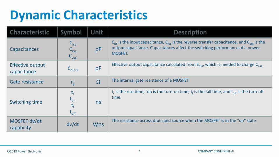
Characteristic Symbol Unit Description
Capacitances Ciss Crss Coss
pF Ciss is the input capacitance, Crss is the reverse transfer capacitance, and Coss is the output capacitance. Capacitances affect the switching performance of a power MOSFET.
Effective output capacitance Co(er) pF
Effective output capacitance calculated from Eoss, which is needed to charge Coss
Gate resistance rg Ω The internal gate resistance of a MOSFET
Switching time
tr ton tf
toff
ns
tr is the rise time, ton is the turn-on time, tf is the fall time, and toff is the turn-off time.
MOSFET dv/dt capability dv/dt V/ns
The resistance across drain and source when the MOSFET is in the "on" state
Dynamic Characteristics
4 ©2019 Power Electronic COMPANY CONFIDENTIAL

A power MOSFET, the gate is insulated by a thin silicon oxide. Capacitances
Gate-Drain gate-drain capacitance Cgd
The structure of the gate electrode Gate-Source
gate-source capacitance Cgs
The structure of the gate electrode
Drain-Source terminal drain-source capacitance Cds
vertical p-n junction.
Capacitance characteristics
5 ©2019 Power Electronic COMPANY CONFIDENTIAL

Input capacitance Ciss = Cgd+Cgs
Output capacitance Coss = Cds+Cgd
Reverse transfer capacitance Crss = Cgd
Capacitance characteristics
6 ©2019 Power Electronic COMPANY CONFIDENTIAL
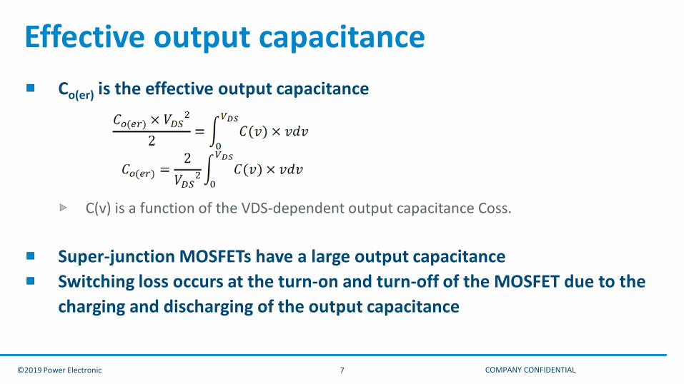
Co(er) is the effective output capacitance
C(v) is a function of the VDS-dependent output capacitance Coss.
Super-junction MOSFETs have a large output capacitance Switching loss occurs at the turn-on and turn-off of the MOSFET due to the charging and discharging of the output capacitance
Effective output capacitance
7 ©2019 Power Electronic COMPANY CONFIDENTIAL

Power MOSFETs are majority-carrier devices Faster and capable of switching at higher frequencies
Switching characteristics
8 ©2019 Power Electronic COMPANY CONFIDENTIAL
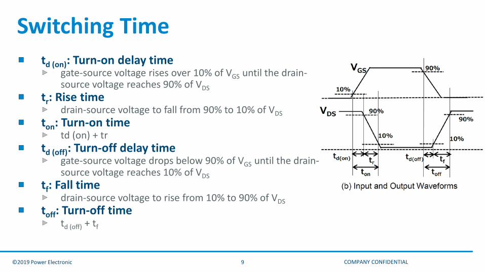
td (on): Turn-on delay time gate-source voltage rises over 10% of VGS until the drain-source voltage reaches 90% of VDS
tr: Rise time drain-source voltage to fall from 90% to 10% of VDS
ton: Turn-on time td (on) + tr
td (off): Turn-off delay time gate-source voltage drops below 90% of VGS until the drain-source voltage reaches 10% of VDS
tf: Fall time drain-source voltage to rise from 10% to 90% of VDS
toff: Turn-off time td (off) + tf
Switching Time
9 ©2019 Power Electronic COMPANY CONFIDENTIAL
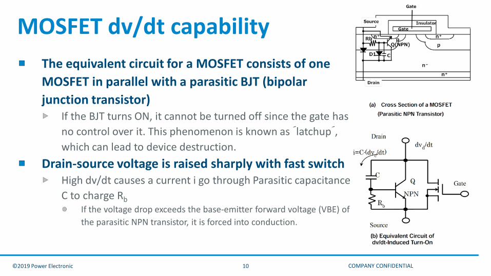
The equivalent circuit for a MOSFET consists of one MOSFET in parallel with a parasitic BJT (bipolar junction transistor)
If the BJT turns ON, it cannot be turned off since the gate has no control over it. This phenomenon is known as ´latchup´, which can lead to device destruction.
Drain-source voltage is raised sharply with fast switch High dv/dt causes a current i go through Parasitic capacitance C to charge Rb
If the voltage drop exceeds the base-emitter forward voltage (VBE) of the parasitic NPN transistor, it is forced into conduction.
MOSFET dv/dt capability
10 ©2019 Power Electronic COMPANY CONFIDENTIAL
Charge Characteristics
11 ©2019 Power Electronic COMPANY CONFIDENTIAL
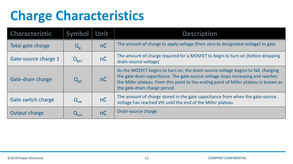
Characteristic Symbol Unit Description Total gate charge Qg nC The amount of charge to apply voltage (from zero to designated voltage) to gate
Gate-source charge 1 Qgs1 nC The amount of charge required for a MOSFET to begin to turn on (before dropping drain-source voltage)
Gate-drain charge Qgd nC As the MOSFET begins to turn on, the drain-source voltage begins to fall, charging the gate-drain capacitance. The gate-source voltage stops increasing and reaches the Miller plateau. From this point to the ending point of Miller plateau is known as the gate-drain charge period.
Gate switch charge Qsw nC The amount of charge stored in the gate capacitance from when the gate-source voltage has reached Vth until the end of the Miller plateau
Output charge Qoss nC Drain-source charge

A power MOSFET turn on, a current flows to the gate, charging the gate-source and gate-drain capacitances. The gate charge (Qgs + Qgd) is the bare minimum charge required to switch the device on
Qg = C x V and Ig = C x dv/dt, the Qg = Time x current
Qg = ig x t
Gate charge
12 ©2019 Power Electronic COMPANY CONFIDENTIAL
Source-Drain Characteristics
13 ©2019 Power Electronic COMPANY CONFIDENTIAL
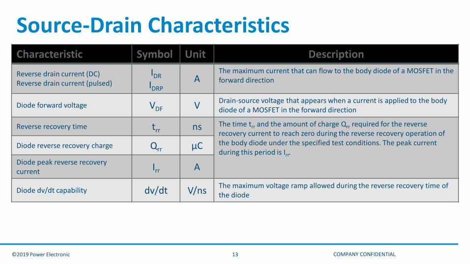
Characteristic Symbol Unit Description Reverse drain current (DC) Reverse drain current (pulsed)
IDR IDRP
A The maximum current that can flow to the body diode of a MOSFET in the forward direction
Diode forward voltage VDF V Drain-source voltage that appears when a current is applied to the body diode of a MOSFET in the forward direction
Reverse recovery time trr ns The time trr and the amount of charge Qrr required for the reverse recovery current to reach zero during the reverse recovery operation of the body diode under the specified test conditions. The peak current during this period is Irr.
Diode reverse recovery charge Qrr μC Diode peak reverse recovery current Irr A
Diode dv/dt capability dv/dt V/ns The maximum voltage ramp allowed during the reverse recovery time of the diode

MOSFET has a equivalent diode structure between source and drain Reverse breakdown voltage is same as drain-source voltage VDSS
Body Diode Characteristics
14 ©2019 Power Electronic COMPANY CONFIDENTIAL
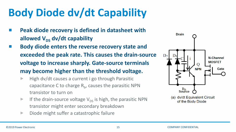
Peak diode recovery is defined in datasheet with allowed VDS dv/dt capability Body diode enters the reverse recovery state and exceeded the peak rate. This causes the drain-source voltage to increase sharply. Gate-source terminals may become higher than the threshold voltage.
High dv/dt causes a current i go through Parasitic capacitance C to charge Rb, causes the parasitic NPN transistor to turn on If the drain-source voltage VDS is high, the parasitic NPN transistor might enter secondary breakdown Diode might suffer a catastrophic failure
Body Diode dv/dt Capability
15 ©2019 Power Electronic COMPANY CONFIDENTIAL