Power Module With 5.5-V Maximum Input Voltage for ... · • Single Exposed Pad and Standard Pinout...
36
VIN EN GND FB VOUT LMZ10505EXT VIN VOUT SS Cin CO Rfbt Rcomp Ccomp Rfbb CSS 1 2 3 4, EP 5 6, 7 Product Folder Sample & Buy Technical Documents Tools & Software Support & Community LMZ10505EXT SNVS669H – JUNE 2010 – REVISED SEPTEMBER 2015 LMZ10505EXT 5-A SIMPLE SWITCHER ® Power Module With 5.5-V Maximum Input Voltage for Demanding and Rugged Applications 1 Features 2 Applications 1• Integrated Shielded Inductor • Point-of-Load Conversions from 3.3-V and 5-V Rails • Flexible Start-up Sequencing Using External Soft- Start, Tracking, and Precision Enable • Space-Constrained Applications • Protection Against In-Rush Currents and Faults • Noise-Sensitive Applications (Such as Such as Input UVLO and Output Short-Circuit Transceiver, Medical) • Single Exposed Pad and Standard Pinout for Easy 3 Description Mounting and Manufacturing The LMZ10505EXT SIMPLE SWITCHER ® power • Pin-to-Pin Compatible With module is a complete, easy-to-use, DC-DC solution – LMZ10503EXT (3-A/15-W Maximum) capable of driving up to a 5-A load with exceptional – LMZ10504EXT (4-A/20-W Maximum) power conversion efficiency, output voltage accuracy, line and load regulation. The LMZ10505EXT is • Fast Transient Response for Powering FPGAs available in an innovative package that enhances and ASICs thermal performance and allows for hand or machine • Electrical Specifications soldering. – 25-W Maximum Total Output Power The LMZ10505EXT can accept an input voltage rail – Up to 5-A Output Current between 2.95 V and 5.5 V, and can deliver an – Input Voltage Range 2.95 V to 5.5 V adjustable and highly accurate output voltage as low as 0.8 V. 1-MHz fixed-frequency PWM switching – Output Voltage Range 0.8 V to 5 V provides a predictable EMI characteristic. Two – ±1.63% Feedback Voltage Accuracy Over external compensation components can be adjusted Temperature to set the fastest response time, while allowing the • Performance Benefits option to use ceramic or electrolytic output capacitors. Externally programmable soft-start capacitor – Operates at High Ambient Temperatures facilitates controlled start-up. The LMZ10505EXT is a – Low Radiated Emissions (EMI) Tested to reliable and robust solution with the following EN55022 Class B Standard features: lossless cycle-by-cycle peak current limit to – Passes 10-V/m Radiated Immunity EMI Tested protect for overcurrent or short-circuit fault, thermal shutdown, input undervoltage lockout, and prebiased to Standard EN61000 4-3 start-up. The LMZ10505EXT is also fully-enabled for – Passes Vibration Standard WEBENCH ® and Power Designer tools. – MIL-STD-883 Method 2007.2 Condition A Device Information (1)(2) – JESD22-B103B Condition 1 PART NUMBER PACKAGE BODY SIZE (NOM) – Passes Drop Standard LMZ10505EXT TO-PMOD (7) 9.85 mm × 10.16 mm – MIL-STD-883 Method 2002.3 Condition B (1) For all available packages, see the orderable addendum at – JESD22-B110 Condition B the end of the data sheet. NOTE: EN 55022:2006, +A1:2007, FCC Part 15 Subpart B: 2007. (2) Peak reflow temperature equals 245°C. See SNAA214 for See Figure 28 and layout for information on device under more details. test. Typical Application Circuit Efficiency V OUT = 3.3 V 1 An IMPORTANT NOTICE at the end of this data sheet addresses availability, warranty, changes, use in safety-critical applications, intellectual property matters and other important disclaimers. PRODUCTION DATA.
Transcript of Power Module With 5.5-V Maximum Input Voltage for ... · • Single Exposed Pad and Standard Pinout...
VIN
EN
GND
FB
VOUT
LMZ10505EXT
VIN VOUT
SS
Cin
CO
Rfbt
Rcomp CcompRfbb
CSS
1
2
3 4, EP
5
6, 7
Product
Folder
Sample &Buy
Technical
Documents
Tools &
Software
Support &Community
LMZ10505EXTSNVS669H –JUNE 2010–REVISED SEPTEMBER 2015
LMZ10505EXT 5-A SIMPLE SWITCHER® Power Module With 5.5-V Maximum Input Voltagefor Demanding and Rugged Applications
1 Features 2 Applications1• Integrated Shielded Inductor • Point-of-Load Conversions from 3.3-V and 5-V
Rails• Flexible Start-up Sequencing Using External Soft-Start, Tracking, and Precision Enable • Space-Constrained Applications
• Protection Against In-Rush Currents and Faults • Noise-Sensitive Applications (Such asSuch as Input UVLO and Output Short-Circuit Transceiver, Medical)
• Single Exposed Pad and Standard Pinout for Easy3 DescriptionMounting and ManufacturingThe LMZ10505EXT SIMPLE SWITCHER® power• Pin-to-Pin Compatible Withmodule is a complete, easy-to-use, DC-DC solution
– LMZ10503EXT (3-A/15-W Maximum) capable of driving up to a 5-A load with exceptional– LMZ10504EXT (4-A/20-W Maximum) power conversion efficiency, output voltage accuracy,
line and load regulation. The LMZ10505EXT is• Fast Transient Response for Powering FPGAsavailable in an innovative package that enhancesand ASICsthermal performance and allows for hand or machine• Electrical Specifications soldering.
– 25-W Maximum Total Output PowerThe LMZ10505EXT can accept an input voltage rail
– Up to 5-A Output Current between 2.95 V and 5.5 V, and can deliver an– Input Voltage Range 2.95 V to 5.5 V adjustable and highly accurate output voltage as low
as 0.8 V. 1-MHz fixed-frequency PWM switching– Output Voltage Range 0.8 V to 5 Vprovides a predictable EMI characteristic. Two– ±1.63% Feedback Voltage Accuracy Over external compensation components can be adjusted
Temperature to set the fastest response time, while allowing the• Performance Benefits option to use ceramic or electrolytic output capacitors.
Externally programmable soft-start capacitor– Operates at High Ambient Temperaturesfacilitates controlled start-up. The LMZ10505EXT is a– Low Radiated Emissions (EMI) Tested to reliable and robust solution with the following
EN55022 Class B Standard features: lossless cycle-by-cycle peak current limit to– Passes 10-V/m Radiated Immunity EMI Tested protect for overcurrent or short-circuit fault, thermal
shutdown, input undervoltage lockout, and prebiasedto Standard EN61000 4-3start-up. The LMZ10505EXT is also fully-enabled for– Passes Vibration Standard WEBENCH® and Power Designer tools.
– MIL-STD-883 Method 2007.2 Condition ADevice Information(1)(2)– JESD22-B103B Condition 1
PART NUMBER PACKAGE BODY SIZE (NOM)– Passes Drop StandardLMZ10505EXT TO-PMOD (7) 9.85 mm × 10.16 mm– MIL-STD-883 Method 2002.3 Condition B(1) For all available packages, see the orderable addendum at– JESD22-B110 Condition B
the end of the data sheet.NOTE: EN 55022:2006, +A1:2007, FCC Part 15 Subpart B: 2007. (2) Peak reflow temperature equals 245°C. See SNAA214 forSee Figure 28 and layout for information on device under more details.test.
Typical Application Circuit Efficiency VOUT = 3.3 V
1
An IMPORTANT NOTICE at the end of this data sheet addresses availability, warranty, changes, use in safety-critical applications,intellectual property matters and other important disclaimers. PRODUCTION DATA.

LMZ10505EXTSNVS669H –JUNE 2010–REVISED SEPTEMBER 2015 www.ti.com
Table of Contents8.1 Application Information............................................ 141 Features .................................................................. 18.2 Typical Applications ................................................ 142 Applications ........................................................... 18.3 System Examples ................................................... 203 Description ............................................................. 1
9 Power Supply Recommendations ...................... 234 Revision History..................................................... 210 Layout................................................................... 235 Pin Configuration and Functions ......................... 3
10.1 Layout Guidelines ................................................. 236 Specifications......................................................... 410.2 Layout Examples................................................... 246.1 Absolute Maximum Ratings ...................................... 410.3 Estimate Power Dissipation and Thermal6.2 ESD Ratings.............................................................. 4 Considerations ......................................................... 27
6.3 Recommended Operating Conditions....................... 4 10.4 Power Module SMT Guidelines ............................ 286.4 Thermal Information .................................................. 4 11 Device and Documentation Support ................. 296.5 Electrical Characteristics........................................... 5
11.1 Device Support...................................................... 296.6 Typical Characteristics .............................................. 711.2 Documentation Support ........................................ 297 Detailed Description ............................................ 10 11.3 Community Resources.......................................... 29
7.1 Overview ................................................................. 10 11.4 Trademarks ........................................................... 297.2 Functional Block Diagram ....................................... 10 11.5 Electrostatic Discharge Caution............................ 297.3 Feature Description................................................. 10 11.6 Glossary ................................................................ 297.4 Device Functional Modes........................................ 13 12 Mechanical, Packaging, and Orderable8 Application and Implementation ........................ 14 Information ........................................................... 30
4 Revision HistoryNOTE: Page numbers for previous revisions may differ from page numbers in the current version.
Changes from Revision G (October 2013) to Revision H Page
• Added ESD Ratings table, Feature Description section, Device Functional Modes, Application and Implementationsection, Power Supply Recommendations section, Layout section, Device and Documentation Support section, andMechanical, Packaging, and Orderable Information section. ................................................................................................ 1
Changes from Revision F (April 2013) to Revision G Page
• Deleted 10 mils....................................................................................................................................................................... 4• Changed 10 mils................................................................................................................................................................... 23• Changed 10 mils................................................................................................................................................................... 27• Added Power Module SMT Guidelines................................................................................................................................. 28
2 Submit Documentation Feedback Copyright © 2010–2015, Texas Instruments Incorporated
Product Folder Links: LMZ10505EXT

Exposed Pad Connect to GND
5 FB
6 VOUT
3 SS
1 VIN
2 EN
4 GND
7 VOUT
LMZ10505EXTwww.ti.com SNVS669H –JUNE 2010–REVISED SEPTEMBER 2015
5 Pin Configuration and Functions
NDW Package7-Lead TO-PMOD
Top View
Pin FunctionsPIN
TYPE DESCRIPTIONNAME NO.EN 2 Analog Active-high enable input for the device.
Exposed pad thermal connection. Connect this pad to the PC board ground plane in order toExposed Pad — Ground reduce thermal resistance value. It also provides an electrical connection to the input and
output capacitors ground terminals.Feedback pin. This is the inverting input of the error amplifier used for sensing the outputFB 5 Analog voltage.Power ground and signal ground. Connect the bottom feedback resistor between this pin andGND 4 Ground the feedback pin.Soft-start control pin. An internal 2-uA current source charges and external capacitor
SS 3 Analog connected between this pin and GND (pin 4) to set the output voltage ramp rate duringstartup. This pin can also be used to configure the tracking feature.A low-ESR input capacitance should be located as close as possible to VIN pin and GNDVIN 1 Power pin.This is the output of the internal inductor. Connect an external resistor voltage divider fromVOUT 6, 7 Power VOUT to FB to ground.
Copyright © 2010–2015, Texas Instruments Incorporated Submit Documentation Feedback 3
Product Folder Links: LMZ10505EXT

LMZ10505EXTSNVS669H –JUNE 2010–REVISED SEPTEMBER 2015 www.ti.com
6 Specifications
6.1 Absolute Maximum Ratings (1) (2)
MIN MAX UNITVIN, VOUT, EN, FB, SS to GND –0.3 6 VPower Dissipation Internally LimitedJunction Temperature 150 °CPeak Reflow Case Temperature (30 sec) 245 °CStorage Temperature, Tstg –65 150 °C
(1) Stresses beyond those listed under Absolute Maximum Ratings may cause permanent damage to the device. These are stress ratingsonly, which do not imply functional operation of the device at these or any other conditions beyond those indicated under RecommendedOperating Conditions. Exposure to absolute-maximum-rated conditions for extended periods may affect device reliability.
(2) For soldering specifications, refer to the following document: SNOA549
6.2 ESD RatingsVALUE UNIT
V(ESD) Electrostatic discharge Human body model (HBM), per ANSI/ESDA/JEDEC JS-001 (1) (2) ±2000 V
(1) JEDEC document JEP155 states that 500-V HBM allows safe manufacturing with a standard ESD control process.(2) The human body model is a 100-pF capacitor discharged through a 1.5-kΩ resistor into each pin. Test method is per JESD22-AI14S.
6.3 Recommended Operating Conditionsover operating free-air temperature range (unless otherwise noted)
MIN MAX UNITVIN to GND 2.95 5.5 VJunction Temperature (TJ) –55 125 °C
6.4 Thermal InformationLMZ10505EXT
THERMAL METRIC (1) NDW (TO-PMOD) UNIT7 PINS
RθJA Junction-to-ambient thermal resistance (2) 20 °C/WRθJC(top) Junction-to-case (top) thermal resistance (no air flow) 1.9 °C/W
(1) For more information about traditional and new thermal metrics, see the Semiconductor and IC Package Thermal Metrics applicationreport, SPRA953.
(2) RθJA measured on a 2.25-in x 2.25-in (5.8 cm x 5.8 cm) 4-layer board, with 1-oz. copper, thirty six thermal vias, no air flow, and 1-Wpower dissipation. Refer to Evaluation Board Application Note: AN-2074 SNVA450.
4 Submit Documentation Feedback Copyright © 2010–2015, Texas Instruments Incorporated
Product Folder Links: LMZ10505EXT

LMZ10505EXTwww.ti.com SNVS669H –JUNE 2010–REVISED SEPTEMBER 2015
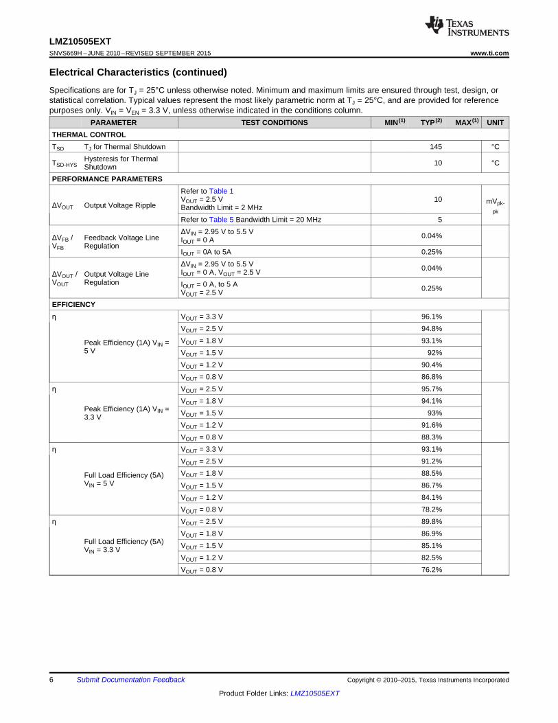
6.5 Electrical CharacteristicsSpecifications are for TJ = 25°C unless otherwise noted. Minimum and maximum limits are ensured through test, design, orstatistical correlation. Typical values represent the most likely parametric norm at TJ = 25°C, and are provided for referencepurposes only. VIN = VEN = 3.3 V, unless otherwise indicated in the conditions column.
PARAMETER TEST CONDITIONS MIN (1) TYP (2) MAX (1) UNITSYSTEM PARAMETERS
0.8Total Feedback Voltage VIN = 2.95 V to 5.5 V
over the operating junctionV FB Variation Including Line and VOUT = 2.5 V Vtemperature range TJ of 0.78 0.82Load Regulation IOUT = 0 A to 5 A–55°C to 125°C
0.8VIN = 3.3 V, VOUT = 2.5
over the operating junctionV FB Feedback Voltage Variation V Vtemperature range TJ of 0.787 0.812IOUT = 0 A–55°C to 125°C
0.798VIN = 3.3 V, VOUT = 2.5
over the operating junctionV FB Feedback Voltage Variation V Vtemperature range TJ of 0.785 0.81IOUT = 5 A–55°C to 125°C
2.6over the operating junctionRisingtemperature range TJ of 2.95–55°C to 125°CVIN(UVL Input UVLO Threshold V
O) (Measured at VIN pin) 2.4over the operating junctionFallingtemperature range TJ of 1.95–55°C to 125°C
ISS Soft-Start Current Charging Current 2 µA1.55
Non-Switching Input over the operating junctionIQ VFB = 1 V mACurrent temperature range TJ of 3–55°C to 125°C
267Shutdown Quiescent over the operating junctionISD VIN = 5.5 V, VEN = 0 V µACurrent temperature range TJ of 500
–55°C to 125°C7.3
Output Current Limit over the operating junctionIOCL VOUT = 2.5 V A(Average Current) temperature range TJ of 5.1 8.7–55°C to 125°C
fFB Frequency Fold-back In current limit 250 kHzPWM SECTION
1000fSW Switching Frequency kHzover the operating junction temperature range TJ of 700 1160–55°C to 125°C
over the operating junction temperature range TJ ofDrange PWM Duty Cycle Range 0% 100%–55°C to 125°CENABLE CONTROL
1.23VEN-IH EN Pin Rising Threshold Vover the operating junction temperature range TJ of 1.8–55°C to 125°C
1.06VEN-IF EN Pin Falling Threshold Vover the operating junction temperature range TJ of 0.8–55°C to 125°C
(1) Minimum and maximum limits are 100% production tested at an ambient temperature (TA) of 25°C. Limits over the operatingtemperature range are ensured through correlation using Statistical Quality Control (SQC) methods. Limits are used to calculateAverage Outgoing Quality Level (AOQL).
(2) Typical numbers are at 25°C and represent the most likely parametric normal.
Copyright © 2010–2015, Texas Instruments Incorporated Submit Documentation Feedback 5
Product Folder Links: LMZ10505EXT
LMZ10505EXTSNVS669H –JUNE 2010–REVISED SEPTEMBER 2015 www.ti.com
Electrical Characteristics (continued)Specifications are for TJ = 25°C unless otherwise noted. Minimum and maximum limits are ensured through test, design, orstatistical correlation. Typical values represent the most likely parametric norm at TJ = 25°C, and are provided for referencepurposes only. VIN = VEN = 3.3 V, unless otherwise indicated in the conditions column.
PARAMETER TEST CONDITIONS MIN (1) TYP (2) MAX (1) UNITTHERMAL CONTROLTSD TJ for Thermal Shutdown 145 °C
Hysteresis for ThermalTSD-HYS 10 °CShutdownPERFORMANCE PARAMETERS
Refer to Table 1VOUT = 2.5 V 10 mVpk-ΔVOUT Output Voltage Ripple Bandwidth Limit = 2 MHz pkRefer to Table 5 Bandwidth Limit = 20 MHz 5ΔVIN = 2.95 V to 5.5 V 0.04%ΔVFB / Feedback Voltage Line IOUT = 0 A
VFB RegulationIOUT = 0A to 5A 0.25%ΔVIN = 2.95 V to 5.5 V 0.04%IOUT = 0 A, VOUT = 2.5 VΔVOUT / Output Voltage Line
VOUT Regulation IOUT = 0 A, to 5 A 0.25%VOUT = 2.5 VEFFICIENCYη VOUT = 3.3 V 96.1%
VOUT = 2.5 V 94.8%VOUT = 1.8 V 93.1%Peak Efficiency (1A) VIN =
5 V VOUT = 1.5 V 92%VOUT = 1.2 V 90.4%VOUT = 0.8 V 86.8%
η VOUT = 2.5 V 95.7%VOUT = 1.8 V 94.1%
Peak Efficiency (1A) VIN = VOUT = 1.5 V 93%3.3 VVOUT = 1.2 V 91.6%VOUT = 0.8 V 88.3%
η VOUT = 3.3 V 93.1%VOUT = 2.5 V 91.2%VOUT = 1.8 V 88.5%Full Load Efficiency (5A)
VIN = 5 V VOUT = 1.5 V 86.7%VOUT = 1.2 V 84.1%VOUT = 0.8 V 78.2%
η VOUT = 2.5 V 89.8%VOUT = 1.8 V 86.9%
Full Load Efficiency (5A) VOUT = 1.5 V 85.1%VIN = 3.3 VVOUT = 1.2 V 82.5%VOUT = 0.8 V 76.2%
6 Submit Documentation Feedback Copyright © 2010–2015, Texas Instruments Incorporated
Product Folder Links: LMZ10505EXT
LMZ10505EXTwww.ti.com SNVS669H –JUNE 2010–REVISED SEPTEMBER 2015
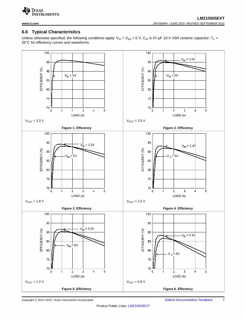
6.6 Typical CharacteristicsUnless otherwise specified, the following conditions apply: VIN = VEN = 5 V, CIN is 47-µF 10-V X5R ceramic capacitor; TA =25°C for efficiency curves and waveforms.
VOUT = 3.3 V VOUT = 2.5 V
Figure 1. Efficiency Figure 2. Efficiency
VOUT = 1.8 V VOUT = 1.5 V
Figure 3. Efficiency Figure 4. Efficiency
VOUT = 1.2 V VOUT = 0.8 V
Figure 5. Efficiency Figure 6. Efficiency
Copyright © 2010–2015, Texas Instruments Incorporated Submit Documentation Feedback 7
Product Folder Links: LMZ10505EXT

LMZ10505EXTSNVS669H –JUNE 2010–REVISED SEPTEMBER 2015 www.ti.com
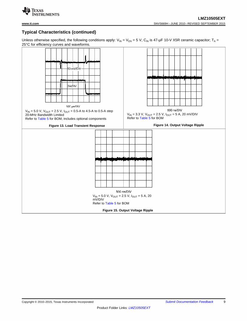
Typical Characteristics (continued)Unless otherwise specified, the following conditions apply: VIN = VEN = 5 V, CIN is 47-µF 10-V X5R ceramic capacitor; TA =25°C for efficiency curves and waveforms.
VIN = 5 V, RθJA = 20°C/W VIN = 3.3 V, RθJA = 20°C/W
Figure 7. Current Derating Figure 8. Current Derating
VOUT = 2.5 V, IOUT = 0 A
VIN = 5 V, VOUT = 2.5 V, IOUT = 5 AEvaluation Board
Figure 10. Start-UpFigure 9. Radiated Emissions (EN 55022, Class B)
VOUT = 2.5 V, IOUT = 0 AVIN = 3.3 V, VOUT = 2.5 V, IOUT = 0.5-A to 4.5-A to 0.5-A step20-MHz Bandwidth LimitedRefer to Table 5 for BOM, includes optional components
Figure 12. Load Transient ResponseFigure 11. Prebiased Start-Up
8 Submit Documentation Feedback Copyright © 2010–2015, Texas Instruments Incorporated
Product Folder Links: LMZ10505EXT
LMZ10505EXTwww.ti.com SNVS669H –JUNE 2010–REVISED SEPTEMBER 2015
Typical Characteristics (continued)Unless otherwise specified, the following conditions apply: VIN = VEN = 5 V, CIN is 47-µF 10-V X5R ceramic capacitor; TA =25°C for efficiency curves and waveforms.
VIN = 5.0 V, VOUT = 2.5 V, IOUT = 0.5-A to 4.5-A to 0.5-A stepVIN = 3.3 V, VOUT = 2.5 V, IOUT = 5 A, 20 mV/DIV20-MHz Bandwidth LimitedRefer to Table 5 for BOMRefer to Table 5 for BOM, includes optional components
Figure 14. Output Voltage RippleFigure 13. Load Transient Response
VIN = 5.0 V, VOUT = 2.5 V, IOUT = 5 A, 20mV/DIVRefer to Table 5 for BOM
Figure 15. Output Voltage Ripple
Copyright © 2010–2015, Texas Instruments Incorporated Submit Documentation Feedback 9
Product Folder Links: LMZ10505EXT

trkb trktIN ULVO
trkt
R RV V
R( ) 1.23
´
= ´
LMZ10505EXTSNVS669H –JUNE 2010–REVISED SEPTEMBER 2015 www.ti.com
7 Detailed Description
7.1 OverviewThe LMZ10505EXT SIMPLE SWITCHER power module is a complete, easy-to-use DC-DC solution capable ofdriving up to a 5-A load with exceptional power conversion efficiency, output voltage accuracy, line and loadregulation. The LMZ10505EXT is available in an innovative package that enhances thermal performance andallows for hand or machine soldering. The LMZ10505EXT is a reliable and robust solution with the followingfeatures: lossless cycle-by-cycle peak current limit to protect for overcurrent or short-circuit fault, thermalshutdown, input undervoltage lockout, and prebiased start-up.
7.2 Functional Block Diagram
7.3 Feature Description
7.3.1 EnableThe LMZ10505EXT features an enable (EN) pin and associated comparator to allow the user to easily sequencethe LMZ10505EXT from an external voltage rail, or to manually set the input UVLO threshold. The turnon orrising threshold and hysteresis for this comparator are typically 1.23 V and 0.15 V, respectively. The precisereference for the enable comparator allows the user to ensure that the LMZ10505EXT will be disabled when thesystem demands it to be.
The EN pin should not be left floating. For always-on operation, connect EN to VIN.
7.3.2 Enable and UVLOUsing a resistor divider from VIN to EN as shown in the schematic diagram below, the input voltage at which thepart begins switching can be increased above the normal input UVLO level according to:
(1)
For example, suppose that the required input UVLO level is 3.69 V. Choosing Renb = 10 kΩ, then we calculateRent = 20 kΩ.
10 Submit Documentation Feedback Copyright © 2010–2015, Texas Instruments Incorporated
Product Folder Links: LMZ10505EXT

SSC nF / ms2.5=
CSS =tSS x ISS
VREF
VIN
EN
GND
VOUT
Renb
Rent
VIN
Cin1
Master Power Supply
VOUT1
VOUT2
CO1LMZ10505EXT
VIN
EN
GND
LMZ10505EXT
Renb
Rent
VIN
Cin1
LMZ10505EXTwww.ti.com SNVS669H –JUNE 2010–REVISED SEPTEMBER 2015
Feature Description (continued)
Figure 16. Setting Enable and UVLO
Alternatively, the EN pin can be driven from another voltage source to cater to system sequencing requirementscommonly found in FPGA and other multi-rail applications. The following schematic shows an LMZ10505EXTthat is sequenced to start based on the voltage level of a master system rail (VOUT1).
Figure 17. Setting Enable and UVLO Using External Power Supply
7.3.3 Soft-StartThe LMZ10505EXT begins to operate when both the VIN and EN, voltages exceed the rising UVLO and enablethresholds, respectively. A controlled soft-start eliminates inrush currents during start-up and allows the usermore control and flexibility when sequencing the LMZ10505EXT with other power supplies.
In the event of either VIN or EN decreasing below the falling UVLO or enable threshold respectively, the voltageon the soft-start pin is collapsed by discharging the soft-start capacitor by a 14-µA (typical) current sink toground.
7.3.4 Soft-Start CapacitorDetermine the soft-start capacitance with the following relationship:
where• VFB is the internal reference voltage (nominally 0.8 V),• ISS is the soft-start charging current (nominally 2 µA)• and CSS is the external soft-start capacitance. (2)
Thus, the required soft-start capacitor per unit output voltage startup time is given by(3)
For example, a 4-ms soft-start time will yield a 10-nF capacitance. The minimum soft-start capacitance is 680 pF.
Copyright © 2010–2015, Texas Instruments Incorporated Submit Documentation Feedback 11
Product Folder Links: LMZ10505EXT

VO
LTA
GE
TIME
RATIOMETRIC STARTUP
VOUT2
EN
VOUT1
trkttrkb
OUT
RR
V V1 1.0=
-
VIN
EN
GND
SS
Rtrkb
Rtrkt
VIN
Cin1
Master Power SupplyVOUT1
VOUT2
CO1VSS
LMZ10505EXT
VOUT
LMZ10505EXTSNVS669H –JUNE 2010–REVISED SEPTEMBER 2015 www.ti.com
Feature Description (continued)7.3.5 TrackingThe LMZ10505EXT can track the output of a master power supply during soft-start by connecting a resistordivider to the SS pin. In this way, the output voltage slew rate of the LMZ10505EXT will be controlled by amaster supply for loads that require precise sequencing. When the tracking function is used, a small value soft-start capacitor should be connected to the SS pin to alleviate output voltage overshoot when recovering from acurrent limit fault.
Figure 18. Tracking Using External Power Supply
7.3.6 Tracking – Equal Soft-Start TimeOne way to use the tracking feature is to design the tracking resistor divider so that the master supply outputvoltage, VOUT1, and the LMZ10505EXT output voltage, VOUT2, both rise together and reach their target values atthe same time. This is termed ratiometric start-up. For this case, the equation governing the values of trackingdivider resistors Rtrkb and Rtrkt is given by:
(4)
Equation 4 includes an offset voltage, of 200 mV, to ensure that the final value of the SS pin voltage exceeds thereference voltage of the LMZ10505EXT. This offset will cause the LMZ10505EXT output voltage to reachregulation slightly before the master supply. For a value of 33 kΩ, 1% is recommended for Rtrkt as a compromisebetween high-precision and low-quiescent current through the divider while minimizing the effect of the 2-µA soft-start current source.
For example, if the master supply voltage VOUT1 is 3.3 V and the LMZ10505EXT output voltage was 1.8 V, thenthe value of Rtrkb needed to give the two supplies identical soft-start times would be 14.3 kΩ. Figure 19 shows anexample of tracking using equal soft-start time.
Figure 19. Timing Diagram for Tracking Using Equal Soft-Start Time
12 Submit Documentation Feedback Copyright © 2010–2015, Texas Instruments Incorporated
Product Folder Links: LMZ10505EXT
VO
LTA
GE
TIME
SIMULTANEOUS STARTUP
VOUT2
EN
VOUT1
OUT OUT1V 0.8 V2
< ´
trkb trkt
OUT
VR R
V V2
0.8
0.8= ´
-
LMZ10505EXTwww.ti.com SNVS669H –JUNE 2010–REVISED SEPTEMBER 2015
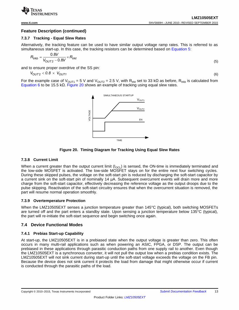
Feature Description (continued)7.3.7 Tracking - Equal Slew RatesAlternatively, the tracking feature can be used to have similar output voltage ramp rates. This is referred to assimultaneous start-up. In this case, the tracking resistors can be determined based on Equation 5:
(5)
and to ensure proper overdrive of the SS pin:(6)
For the example case of VOUT1 = 5 V and VOUT2 = 2.5 V, with Rtrkt set to 33 kΩ as before, Rtrkb is calculated fromEquation 6 to be 15.5 kΩ. Figure 20 shows an example of tracking using equal slew rates.
Figure 20. Timing Diagram for Tracking Using Equal Slew Rates
7.3.8 Current LimitWhen a current greater than the output current limit (IOCL) is sensed, the ON-time is immediately terminated andthe low-side MOSFET is activated. The low-side MOSFET stays on for the entire next four switching cycles.During these skipped pulses, the voltage on the soft-start pin is reduced by discharging the soft-start capacitor bya current sink on the soft-start pin of nominally 14 µA. Subsequent overcurrent events will drain more and morecharge from the soft-start capacitor, effectively decreasing the reference voltage as the output droops due to thepulse skipping. Reactivation of the soft-start circuitry ensures that when the overcurrent situation is removed, thepart will resume normal operation smoothly.
7.3.9 Overtemperature ProtectionWhen the LMZ10505EXT senses a junction temperature greater than 145°C (typical), both switching MOSFETsare turned off and the part enters a standby state. Upon sensing a junction temperature below 135°C (typical),the part will re-initiate the soft-start sequence and begin switching once again.
7.4 Device Functional Modes
7.4.1 Prebias Start-up CapabilityAt start-up, the LMZ10505EXT is in a prebiased state when the output voltage is greater than zero. This oftenoccurs in many multi-rail applications such as when powering an ASIC, FPGA, or DSP. The output can beprebiased in these applications through parasitic conduction paths from one supply rail to another. Even thoughthe LMZ10505EXT is a synchronous converter, it will not pull the output low when a prebias condition exists. TheLMZ10505EXT will not sink current during start-up until the soft-start voltage exceeds the voltage on the FB pin.Because the device does not sink current it protects the load from damage that might otherwise occur if currentis conducted through the parasitic paths of the load.
Copyright © 2010–2015, Texas Instruments Incorporated Submit Documentation Feedback 13
Product Folder Links: LMZ10505EXT

VIN
EN
GND
FB
VIN
VOUT
SS
Cin1
CO1
Rfbt
Rcomp CcompRfbb
CSS
U1
VOUT
LMZ10505EXT
1
2
3 4, EP
5
6, 7
LMZ10505EXTSNVS669H –JUNE 2010–REVISED SEPTEMBER 2015 www.ti.com
8 Application and Implementation
NOTEInformation in the following applications sections is not part of the TI componentspecification, and TI does not warrant its accuracy or completeness. TI’s customers areresponsible for determining suitability of components for their purposes. Customers shouldvalidate and test their design implementation to confirm system functionality.
8.1 Application InformationThe LMZ10505EXT is a step-down DC-to-DC power module. It is typically used to convert a higher DC voltage toa lower DC voltage with a maximum output current of 5 A. The following design procedure can be used to selectcomponents for the LMZ10505EXT. Alternately, the WEBENCH software may be used to generate completedesigns. When generating a design, the WEBENCH software uses iterative design procedure and accessescomprehensive databases of components. Please go to www.ti.com for more details.
8.2 Typical ApplicationsThis section provides several application solutions with an associated bill of materials. The compensation foreach solution was optimized to work over the full input range. Many applications have a fixed input voltage rail. Itis possible to modify the compensation to obtain a faster transient response for a given input voltage operatingpoint.
Figure 21. Typical Application Schematic
8.2.1 Design RequirementsFor this example the following application parameters exist.• VIN = 5 V• VOUT = 2.5 V• IOUT = 5 A• ΔVOUT = 20 mVpk-pk• ΔVo_tran = ±20 mVpk-pk
Table 1. Bill of Materials, VIN = 3.3 V to 5 V, VOUT = 2.5 V, IOUT (MAX) = 5 A,Optimized for Electrolytic Input and Output Capacitance
DESIGNATOR DESCRIPTION CASE SIZE MANUFACTURER MANUFACTURER P/N QUANTITYU1 SIMPLE SWITCHER PFM-7 Texas Instruments LMZ10505EXTTZ 1Cin1 150 µF, 6.3 V, 18 mΩ C2, 6.0 × 3.2 × 1.8 mm Sanyo 6TPE150MIC2 1CO1 330 µF, 6.3 V, 18 mΩ D3L, 7.3 × 4.3 × 2.8 Sanyo 6TPE330MIL 1
mmRfbt 100 kΩ 0603 Vishay Dale CRCW0603100KFKEA 1
14 Submit Documentation Feedback Copyright © 2010–2015, Texas Instruments Incorporated
Product Folder Links: LMZ10505EXT

OUT
IN
VD
V=
OUTin
sw IN
I D DC
f V
(1 )´ ´ -³
´ D
LMZ10505EXTwww.ti.com SNVS669H –JUNE 2010–REVISED SEPTEMBER 2015
Typical Applications (continued)Table 1. Bill of Materials, VIN = 3.3 V to 5 V, VOUT = 2.5 V, IOUT (MAX) = 5 A,
Optimized for Electrolytic Input and Output Capacitance (continued)DESIGNATOR DESCRIPTION CASE SIZE MANUFACTURER MANUFACTURER P/N QUANTITY
Rfbb 47.5 kΩ 0603 Vishay Dale CRCW060347K5FKEA 1Rcomp 15 kΩ 0603 Vishay Dale CRCW060315K0FKEA 1Ccomp 330 pF, ±5%, C0G, 50 V 0603 TDK C1608C0G1H331J 1CSS 10 nF, ±10%, X7R, 16 V 0603 Murata GRM188R71C103KA01 1
Table 2. Bill of Materials, VIN = 3.3 V, VOUT = 0.8 V, IOUT (MAX) = 5 A,Optimized for Solution Size and Transient Response (1)
DESIGNATOR DESCRIPTION CASE SIZE MANUFACTURER MANUFACTURER P/N QUANTITYU1 SIMPLE SWITCHER PFM-7 Texas Instruments LMZ10505EXTTZ 1
Cin1, CO1 47 µF, X5R, 6.3 V 1206 TDK C3216X5R0J476M 2Rfbt 110 kΩ 0402 Vishay Dale CRCW0402100KFKED 1
Rcomp 1.0 kΩ 0402 Vishay Dale CRCW04021K00FKED 1Ccomp 27 pF, ±5%, C0G, 50 V 0402 Murata GRM1555C1H270JZ01 1CSS 10 nF, ±10%, X7R, 16 V 0402 Murata GRM155R71C103KA01 1
(1) In the case where the output voltage is 0.8 V, it is recommended to remove Rfbb and keep Rfbt, Rcomp, and Ccomp for a type IIIcompensation.
8.2.2 Detailed Design ProcedureLMZ10505EXT is fully supported by WEBENCH and offers the following: component selection, performance,electrical, and thermal simulations as well as the Build-It board, for a reduced design time. On the other hand, allexternal components can be calculated by following the design procedure below.1. Determine the input voltage and output voltage. Also, make note of the ripple voltage and voltage transient
requirements.2. Determine the necessary input and output capacitance.3. Calculate the feedback resistor divider.4. Select the optimized compensation component values.5. Estimate the power dissipation and board thermal requirements.6. Follow the PCB design guideline.7. Learn about the LMZ10505EXT features such as enable, input UVLO, soft-start, tracking, prebiased start-up,
current limit, and thermal shutdown.
8.2.2.1 Input Capacitor SelectionA 22-µF or 47-µF high-quality dielectric (X5R, X7R) ceramic capacitor rated at twice the maximum input voltageis typically sufficient. The input capacitor must be placed as close as possible to the VIN pin and GND exposedpad to substantially eliminate the parasitic effects of any stray inductance or resistance on the PCB and supplylines.
Neglecting capacitor equivalent series resistance (ESR), the resultant input capacitor AC ripple voltage is atriangular waveform. The minimum input capacitance for a given peak-to-peak value (ΔVIN) of VIN is specified asfollows:
where• the PWM duty cycle, D, is given by Equation 8: (7)
(8)
Copyright © 2010–2015, Texas Instruments Incorporated Submit Documentation Feedback 15
Product Folder Links: LMZ10505EXT

step FB INO
OUT IN OUT
I V L VC
V V V Vo tran4 ( ) _
´ ´ ´³
´ ´ - ´ D
oC F6³ m
( )o
mAC
× 1 MHz × mV mA × 3 m
833
8 20 833³
é ù- Wë û
V
V
L
V Vi mA
H 1 MHz
2.55
(5 2.5 )833
1.5
- ´D = =
m ´
IN OUTL
sw
V V Di
L f
( )- ´D =
´
[ ]L
O
sw OUT L ESR
iC
f V i R8 ( )
D³
´ ´ D - D ´
Cin RMS
V VI 5A = 2.5A
V V( )
2.5 2.51
5 5
æ ö= ´ -ç ÷
è ø
Cin RMS OUTI I D D( ) (1 )= ´ -
Cin 8
5A x ( ) x (1 - )
1 MHz x 50mV
2.5V5V
2.5V5V
8 25µF
LMZ10505EXTSNVS669H –JUNE 2010–REVISED SEPTEMBER 2015 www.ti.com
If ΔVIN is 1% of VIN, this equals to 50 mV and fSW = 1 MHz
(9)
A second criteria before finalizing the Cin bypass capacitor is the RMS current capability. The necessary RMScurrent rating of the input capacitor to a buck regulator can be estimated by
(10)
(11)
With this high AC current present in the input capacitor, the RMS current rating becomes an importantparameter. The maximum input capacitor ripple voltage and RMS current occur at 50% duty cycle. Select aninput capacitor rated for at least the maximum calculated ICin(RMS).
Additional bulk capacitance with higher ESR may be required to damp any resonance effects of the inputcapacitance and parasitic inductance.
8.2.2.2 Output Capacitor SelectionIn general, 22-µF to 100-µF high quality dielectric (X5R, X7R) ceramic capacitor rated at twice the maximumoutput voltage is sufficient given the optimal high frequency characteristics and low ESR of ceramic dielectrics.Although, the output capacitor can also be of electrolytic chemistry for increased capacitance density.
Two output capacitance equations are required to determine the minimum output capacitance. One equationdetermines the output capacitance (CO) based on PWM ripple voltage. The second equation determines CObased on the load transient characteristics. Select the largest capacitance value of the two.
The minimum capacitance, given the maximum output voltage ripple (ΔVOUT) requirement, is determined by thefollowing equation:
where• and the peak to peak inductor current ripple (ΔiL) is equal to Equation 13: (12)
(13)
RESR is the total output capacitor ESR, L is the inductance value of the internal power inductor, where L = 1.5µH, and fSW = 1 MHz. Therefore, per the design example:
(14)
The minimum output capacitance requirement due to the PWM ripple voltage is:
(15)
(16)
Three mΩ is a typical RESR value for ceramic capacitors.
Equation 17 provides a good first pass capacitance requirement for a load transient:
where• Istep is the peak to peak load step (10% to 90% of the maximum load for this example),• VFB = 0.8 V,
16 Submit Documentation Feedback Copyright © 2010–2015, Texas Instruments Incorporated
Product Folder Links: LMZ10505EXT
fbt fbbOUT
fbb
R RV V
R0.8
+
= ´
oC F48³ m
o
4A × 0.8V × 1.5μH × 5VC
4 × 2.5V × (5V 2.5V) × 20mV³
-
LMZ10505EXTwww.ti.com SNVS669H –JUNE 2010–REVISED SEPTEMBER 2015
• and ΔVo_tran is the maximum output voltage deviation, which is ±20 mV. (17)
Therefore the capacitance requirement for the given design parameters is:
(18)
(19)
In this particular design the output capacitance is determined by the load transient requirements.
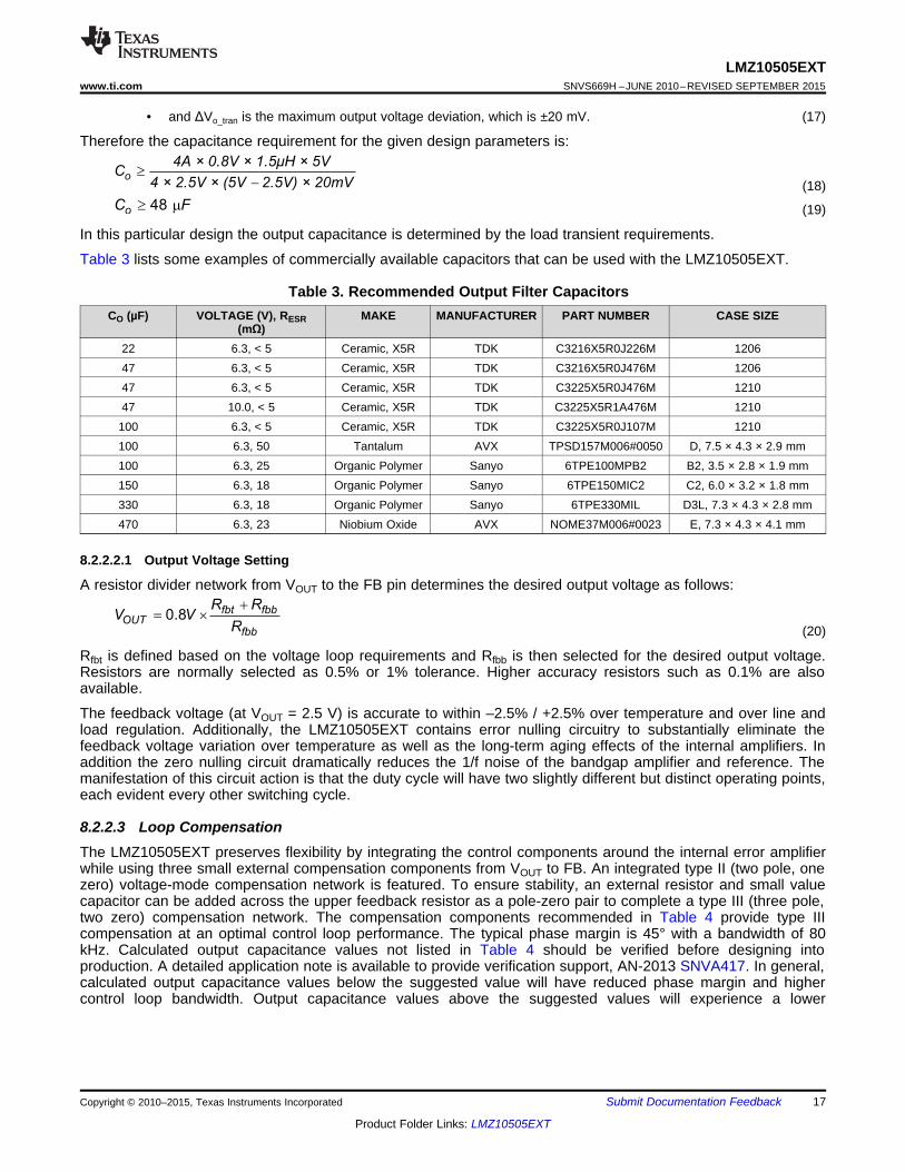
Table 3 lists some examples of commercially available capacitors that can be used with the LMZ10505EXT.
Table 3. Recommended Output Filter CapacitorsCO (µF) VOLTAGE (V), RESR MAKE MANUFACTURER PART NUMBER CASE SIZE
(mΩ)22 6.3, < 5 Ceramic, X5R TDK C3216X5R0J226M 120647 6.3, < 5 Ceramic, X5R TDK C3216X5R0J476M 120647 6.3, < 5 Ceramic, X5R TDK C3225X5R0J476M 121047 10.0, < 5 Ceramic, X5R TDK C3225X5R1A476M 1210
100 6.3, < 5 Ceramic, X5R TDK C3225X5R0J107M 1210100 6.3, 50 Tantalum AVX TPSD157M006#0050 D, 7.5 × 4.3 × 2.9 mm100 6.3, 25 Organic Polymer Sanyo 6TPE100MPB2 B2, 3.5 × 2.8 × 1.9 mm150 6.3, 18 Organic Polymer Sanyo 6TPE150MIC2 C2, 6.0 × 3.2 × 1.8 mm330 6.3, 18 Organic Polymer Sanyo 6TPE330MIL D3L, 7.3 × 4.3 × 2.8 mm470 6.3, 23 Niobium Oxide AVX NOME37M006#0023 E, 7.3 × 4.3 × 4.1 mm
8.2.2.2.1 Output Voltage Setting
A resistor divider network from VOUT to the FB pin determines the desired output voltage as follows:
(20)
Rfbt is defined based on the voltage loop requirements and Rfbb is then selected for the desired output voltage.Resistors are normally selected as 0.5% or 1% tolerance. Higher accuracy resistors such as 0.1% are alsoavailable.
The feedback voltage (at VOUT = 2.5 V) is accurate to within –2.5% / +2.5% over temperature and over line andload regulation. Additionally, the LMZ10505EXT contains error nulling circuitry to substantially eliminate thefeedback voltage variation over temperature as well as the long-term aging effects of the internal amplifiers. Inaddition the zero nulling circuit dramatically reduces the 1/f noise of the bandgap amplifier and reference. Themanifestation of this circuit action is that the duty cycle will have two slightly different but distinct operating points,each evident every other switching cycle.
8.2.2.3 Loop CompensationThe LMZ10505EXT preserves flexibility by integrating the control components around the internal error amplifierwhile using three small external compensation components from VOUT to FB. An integrated type II (two pole, onezero) voltage-mode compensation network is featured. To ensure stability, an external resistor and small valuecapacitor can be added across the upper feedback resistor as a pole-zero pair to complete a type III (three pole,two zero) compensation network. The compensation components recommended in Table 4 provide type IIIcompensation at an optimal control loop performance. The typical phase margin is 45° with a bandwidth of 80kHz. Calculated output capacitance values not listed in Table 4 should be verified before designing intoproduction. A detailed application note is available to provide verification support, AN-2013 SNVA417. In general,calculated output capacitance values below the suggested value will have reduced phase margin and highercontrol loop bandwidth. Output capacitance values above the suggested values will experience a lower
Copyright © 2010–2015, Texas Instruments Incorporated Submit Documentation Feedback 17
Product Folder Links: LMZ10505EXT

VIN
EN
GND
FB
LMZ10505EXTRfbt
Rcomp
Ccomp
Rfbb
VIN
VOUT
LMZ10505EXTSNVS669H –JUNE 2010–REVISED SEPTEMBER 2015 www.ti.com
bandwidth and increased phase margin. Higher bandwidth is associated with faster system response to suddenchanges such as load transients. Phase margin changes the characteristics of the response. Lower phasemargin is associated with underdamped ringing and higher phase margin is associated with overdampedresponse. Losing all phase margin will cause the system to be unstable; an optimized area of operation is 30° to60° of phase margin, with a bandwidth of 100 kHz ±20 kHz.
Figure 22. Loop Compensation Control Components
Table 4. LMZ10505EXT Compensation Component Values (1)
VIN (V) CO (µF) ESR (mΩ) Rfbt (kΩ) Ccomp (pF) Rcomp (kΩ)MIN MAX
22 2 20 200 27 1.547 2 20 124 68 1.4100 1 10 82.5 150 0.681150 1 5 63.4 220 1
5150 10 25 63.4 220 3.48150 26 50 226 62 12.1220 15 30 150 100 6.98220 31 60 316 560 1422 2 20 118 43 9.0947 2 20 76.8 100 3.32100 1 10 49.9 180 2.49150 1 5 40.2 330 1
3.3150 10 25 43.2 330 4.99150 26 50 143 100 7.5220 15 30 100 180 4.99220 31 60 200 100 8.06
(1) In the special case where the output voltage is 0.8V, it is recommended to remove Rfbb and keep Rfbt, Rcomp, and Ccomp for a type IIIcompensation.
18 Submit Documentation Feedback Copyright © 2010–2015, Texas Instruments Incorporated
Product Folder Links: LMZ10505EXT
LMZ10505EXTwww.ti.com SNVS669H –JUNE 2010–REVISED SEPTEMBER 2015
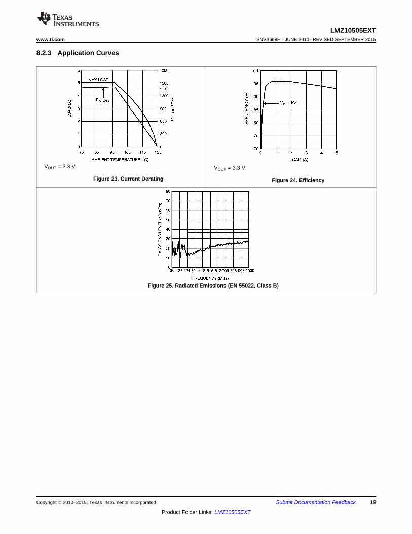
8.2.3 Application Curves
VOUT = 3.3 V VOUT = 3.3 V
Figure 23. Current Derating Figure 24. Efficiency
Figure 25. Radiated Emissions (EN 55022, Class B)
Copyright © 2010–2015, Texas Instruments Incorporated Submit Documentation Feedback 19
Product Folder Links: LMZ10505EXT

VIN
EN
GND
FB
VINVOUT
SS
Cin1
CO1
Rfbt
Rcomp
Ccomp
Rfbb
CSS
U1
VOUT
LMZ10505EXT CO2 CO3
1
2
3 4, EP
5
6, 7Optional
+Cin2
Optional
LMZ10505EXTSNVS669H –JUNE 2010–REVISED SEPTEMBER 2015 www.ti.com
8.3 System Examples
8.3.1 Application Schematic for 3.3-V to 5-V Input and 2.5-V Output With Optimized Ripple and TransientResponse
The compensation for each solution was optimized to work over the stated input range. Many applications have afixed input voltage rail. It is possible to modify the compensation to obtain a faster transient response for a giveninput voltage operating point. This schematic is intended to serve as a helpful starting point towards an optimizeddesign.
Figure 26. Schematic for 2.5-V Output Based on 3.3-V to 5-V Input
Table 5. Bill of Materials, VIN = 3.3 V to 5 V, VOUT = 2.5 V, IOUT (MAX) = 5 A,Optimized for Low Input and Output Ripple Voltage and Fast Transient Response
DESIGNATOR DESCRIPTION CASE SIZE MANUFACTURER MANUFACTURER P/N QUANTITYU1 SIMPLE SWITCHER PFM-7 Texas Instruments LMZ10505EXTTZ 1Cin1 22 µF, X5R, 10 V 1210 AVX 1210ZD226MAT 2Cin2 220 µF, 10 V, AL-Elec E Panasonic EEE1AA221AP 1 (1)
CO1 4.7 µF, X5R, 10 V 0805 AVX 0805ZD475MAT 1 (1)
CO2 22 µF, X5R, 6.3 V 1206 AVX 12066D226MAT 1 (1)
CO3 100 µF, X5R, 6.3 V 1812 AVX 18126D107MAT 1Rfbt 75 kΩ 0402 Vishay Dale CRCW040275K0FKED 1Rfbb 34.8 kΩ 0402 Vishay Dale CRCW040234K8FKED 1
Rcomp 1.0 kΩ 0402 Vishay Dale CRCW04021K00FKED 1Ccomp 100 pF, ±5%, C0G, 50 V 0402 Murata GRM1555C1H101JZ01 1CSS 10 nF, ±10%, X7R, 16 V 0402 Murata GRM155R71C103KA01 1
(1) Optional components, include for low input and output voltage ripple.
Table 6. Output Voltage Setting (Rfbt = 75 kΩ)VOUT Rfbb
2.5 V 34.8 kΩ1.8 V 59 kΩ1.5 V 84.5 kΩ1.2 V 150 kΩ0.9 V 590 kΩ
20 Submit Documentation Feedback Copyright © 2010–2015, Texas Instruments Incorporated
Product Folder Links: LMZ10505EXT

VIN
EN
GND
FB
VINVOUT
SS
Cin1
CO1
Rfbt
Rcomp CcompRfbb
CSS
U1
VOUT
LMZ10505EXT
Cin2Cin3
CO2 CO3
Cin4Cin5+
Ren1
1
2
3 4, EP
5
6, 7
LMZ10505EXTwww.ti.com SNVS669H –JUNE 2010–REVISED SEPTEMBER 2015
8.3.2 Application Schematic for 3.3-V to 5-V Input and 2.5-V OutputThe compensation for each solution was optimized to work over the stated input range. Many applications have afixed input voltage rail. It is possible to modify the compensation to obtain a faster transient response for a giveninput voltage operating point. This schematic is intended to serve as a helpful starting point towards an optimizeddesign.
Figure 27. Schematic for 2.5-V Output Based on 3.3-V to 5-V Input
Table 7. Bill of Materials, VIN = 3.3 V to 5 V, VOUT = 2.5 V, IOUT (MAX) = 5 ADESIGNATOR DESCRIPTION CASE SIZE MANUFACTURER MANUFACTURER P/N QUANTITY
U1 SIMPLE SWITCHER PFM-7 Texas Instruments LMZ10505EXTTZ 1Cin1 1 µF, X7R, 16 V 0805 TDK C2012X7R1C105K 1
Cin2, CO1 4.7 µF, X5R, 6.3 V 0805 TDK C2012X5R0J475K 2Cin3, CO2 22 µF, X5R, 16 V 1210 TDK C3225X5R1C226M 2
Cin4 47 µF, X5R, 6.3 V 1210 TDK C3225X5R0J476M 1Cin5 220 µF, 10 V, AL-Elec E Panasonic EEE1AA221AP 1CO3 100 µF, X5R, 6.3 V 1812 TDK C4532X5R0J107M 1Rfbt 75 kΩ 0805 Vishay Dale CRCW080575K0FKEA 1Rfbb 34.8 kΩ 0805 Vishay Dale CRCW080534K8FKEA 1
Rcomp 1.1 kΩ 0805 Vishay Dale CRCW08051K10FKEA 1Ccomp 180 pF, ±5%, C0G, 50 V 0603 TDK C1608C0G1H181J 1Ren1 100 kΩ 0805 Vishay Dale CRCW0805100KFKEA 1CSS 10 nF, ±5%, C0G, 50 V 0805 TDK C2012C0G1H103J 1
Table 8. Output Voltage Setting (Rfbt = 75 kΩ)VOUT Rfbb
2.5 V 34.8 kΩ1.8 V 59 kΩ1.5 V 84.5 kΩ1.2 V 150 kΩ0.9 V 590 kΩ
Copyright © 2010–2015, Texas Instruments Incorporated Submit Documentation Feedback 21
Product Folder Links: LMZ10505EXT
VIN
EN
GND
FB
VINVOUT
SS
Cin1
CO1
Rfbt
Rcomp CcompRfbb
CSS
U1
VOUT
LMZ10505EXT
Cin2Cin3
1
2
3 4, EP
5
6, 7
LMZ10505EXTSNVS669H –JUNE 2010–REVISED SEPTEMBER 2015 www.ti.com
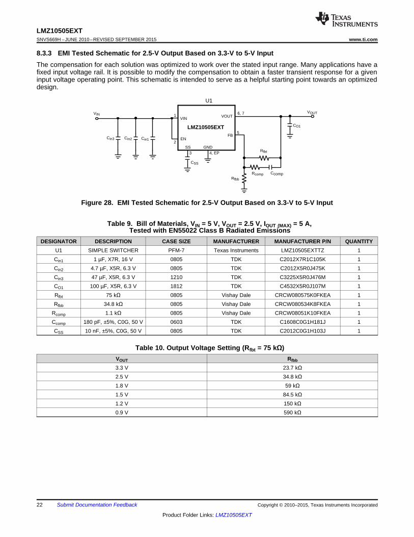
8.3.3 EMI Tested Schematic for 2.5-V Output Based on 3.3-V to 5-V InputThe compensation for each solution was optimized to work over the stated input range. Many applications have afixed input voltage rail. It is possible to modify the compensation to obtain a faster transient response for a giveninput voltage operating point. This schematic is intended to serve as a helpful starting point towards an optimizeddesign.
Figure 28. EMI Tested Schematic for 2.5-V Output Based on 3.3-V to 5-V Input
Table 9. Bill of Materials, VIN = 5 V, VOUT = 2.5 V, IOUT (MAX) = 5 A,Tested with EN55022 Class B Radiated Emissions
DESIGNATOR DESCRIPTION CASE SIZE MANUFACTURER MANUFACTURER P/N QUANTITYU1 SIMPLE SWITCHER PFM-7 Texas Instruments LMZ10505EXTTZ 1Cin1 1 µF, X7R, 16 V 0805 TDK C2012X7R1C105K 1Cin2 4.7 µF, X5R, 6.3 V 0805 TDK C2012X5R0J475K 1Cin3 47 µF, X5R, 6.3 V 1210 TDK C3225X5R0J476M 1CO1 100 µF, X5R, 6.3 V 1812 TDK C4532X5R0J107M 1Rfbt 75 kΩ 0805 Vishay Dale CRCW080575K0FKEA 1Rfbb 34.8 kΩ 0805 Vishay Dale CRCW080534K8FKEA 1
Rcomp 1.1 kΩ 0805 Vishay Dale CRCW08051K10FKEA 1Ccomp 180 pF, ±5%, C0G, 50 V 0603 TDK C1608C0G1H181J 1CSS 10 nF, ±5%, C0G, 50 V 0805 TDK C2012C0G1H103J 1
Table 10. Output Voltage Setting (Rfbt = 75 kΩ)VOUT Rfbb
3.3 V 23.7 kΩ2.5 V 34.8 kΩ1.8 V 59 kΩ1.5 V 84.5 kΩ1.2 V 150 kΩ0.9 V 590 kΩ
22 Submit Documentation Feedback Copyright © 2010–2015, Texas Instruments Incorporated
Product Folder Links: LMZ10505EXT

LMZ10505EXTwww.ti.com SNVS669H –JUNE 2010–REVISED SEPTEMBER 2015
9 Power Supply RecommendationsThe LMZ10505EXT device is designed to operate from an input voltage supply range between 2.95 V and 5.5 V.This input supply should be well regulated and able to withstand maximum input current and maintain a stablevoltage. The resistance of the input supply rail should be low enough that an input current transient does notcause a high enough drop at the LMZ10505EXT supply voltage that can cause a false UVLO fault triggering andsystem reset. If the input supply is more than a few inches from the LMZ10505EXT, additional bulk capacitancemay be required in addition to the ceramic bypass capacitors. The amount of bulk capacitance is not critical, buta 47-μF or 100-μF electrolytic capacitor is a typical choice.
10 Layout
10.1 Layout GuidelinesPCB layout is an important part of DC-DC converter design. Poor board layout can disrupt the performance of aDC-DC converter and surrounding circuitry by contributing to EMI, ground bounce and resistive voltage drop inthe traces. These can send erroneous signals to the DC-DC converter resulting in poor regulation or instability.Good layout can be implemented by following a few simple design rules.1. Minimize area of switched current loops.
From an EMI reduction standpoint, it is imperative to minimize the high di/dt current paths. The high currentthat does not overlap contains high di/dt, see Figure 29. Therefore physically place input capacitor (Cin1) asclose as possible to the LMZ10505EXT VIN pin and GND exposed pad to avoid observable high-frequencynoise on the output pin. This will minimize the high di/dt area and reduce radiated EMI. Additionally,grounding for both the input and output capacitor should consist of a localized top side plane that connects tothe GND exposed pad (EP).
2. Have a single point ground.The ground connections for the feedback, soft-start, and enable components should be routed only to theGND pin of the device. This prevents any switched or load currents from flowing in the analog ground traces.If not properly placed, poor grounding can result in degraded load regulation or erratic output voltage ripplebehavior. Provide the single point ground connection from pin 4 to EP.
3. Minimize trace length to the FB pin.Both feedback resistors, Rfbt and Rfbb, and the compensation components, Rcomp and Ccomp, should belocated close to the FB pin. Because the FB node is high impedance, keep the copper area as small aspossible. This is most important as relatively high-value resistors are used to set the output voltage.
4. Make input and output bus connections as wide as possible.This reduces any voltage drops on the input or output of the converter and maximizes efficiency. To optimizevoltage accuracy at the load, ensure that a separate feedback voltage sense trace is made at the load. Doingso will correct for voltage drops and provide optimum output accuracy.
5. Provide adequate device heat-sinking.Use an array of heat-sinking vias to connect the exposed pad to the ground plane on the bottom PCB layer.If the PCB has multiple copper layers, thermal vias can also be employed to make connection to inner layerheat-spreading ground planes. For best results use a 6 × 6 via array with minimum via diameter of 8 milthermal vias spaced 59 mils (1.5 mm). Ensure enough copper area is used for heat-sinking to keep thejunction temperature below 125°C.
Copyright © 2010–2015, Texas Instruments Incorporated Submit Documentation Feedback 23
Product Folder Links: LMZ10505EXT

SS
FB
GND
VIN
1 2 3 4 5 6 7
Top View
VIN
COUT
VOUT
RENT
GND
Thermal V ias
VOUT
CIN
GND
RENB
CFFRFBT
RFBB
GND Plane
EXPOSED PAD
CSS
EN
VOUT
VIN
GND
VIN
VOUT
Cin1 CO1
Loop 1 Loop 2
LMZ10505EXTVOUT
dIdt
High
LMZ10505EXTSNVS669H –JUNE 2010–REVISED SEPTEMBER 2015 www.ti.com
10.2 Layout ExamplesThe PCB design is available in the LMZ10505EXT product folder at www.ti.com.
Figure 29. Critical Current Loops to Minimize
Figure 30. PCB Layout Guide
24 Submit Documentation Feedback Copyright © 2010–2015, Texas Instruments Incorporated
Product Folder Links: LMZ10505EXT

LMZ10505EXTwww.ti.com SNVS669H –JUNE 2010–REVISED SEPTEMBER 2015
Layout Examples (continued)
Figure 31. Top Copper
Figure 32. Internal Layer 1 (Ground)
Copyright © 2010–2015, Texas Instruments Incorporated Submit Documentation Feedback 25
Product Folder Links: LMZ10505EXT
LMZ10505EXTSNVS669H –JUNE 2010–REVISED SEPTEMBER 2015 www.ti.com
Layout Examples (continued)
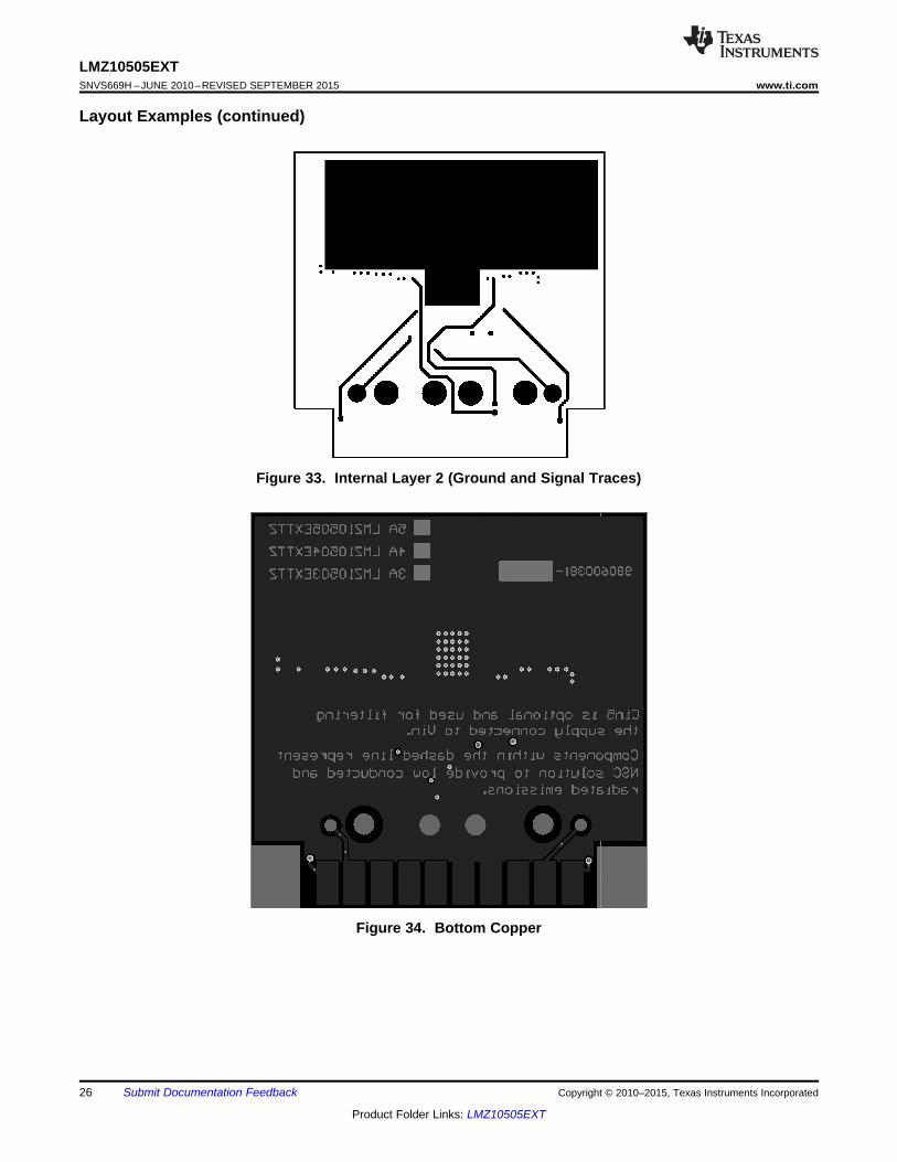
Figure 33. Internal Layer 2 (Ground and Signal Traces)
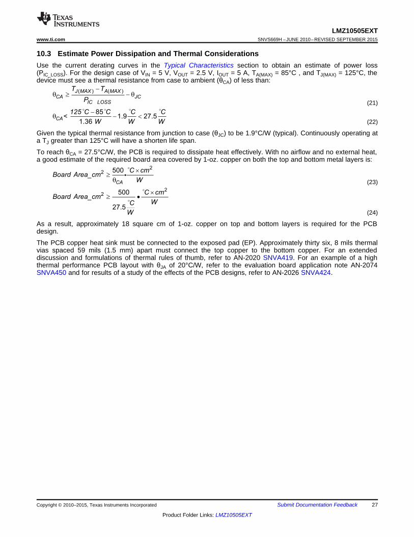
Figure 34. Bottom Copper
26 Submit Documentation Feedback Copyright © 2010–2015, Texas Instruments Incorporated
Product Folder Links: LMZ10505EXT
C cmBoard Area_cm
WC
W
22 500
27.5
´³ ·
o
o
CA
C cmBoard Area_cm
W
22 500 ´
³q
o
g
CA
125 C C C C<
W W W
851.9 27.5
1.36
-q - <
o o o o
J MAX A MAX
CA JC
IC LOSS
T T
P
( ) ( )
_
-q ³ - q
LMZ10505EXTwww.ti.com SNVS669H –JUNE 2010–REVISED SEPTEMBER 2015
10.3 Estimate Power Dissipation and Thermal ConsiderationsUse the current derating curves in the Typical Characteristics section to obtain an estimate of power loss(PIC_LOSS). For the design case of VIN = 5 V, VOUT = 2.5 V, IOUT = 5 A, TA(MAX) = 85°C , and TJ(MAX) = 125°C, thedevice must see a thermal resistance from case to ambient (θCA) of less than:
(21)
(22)
Given the typical thermal resistance from junction to case (θJC) to be 1.9°C/W (typical). Continuously operating ata TJ greater than 125°C will have a shorten life span.
To reach θCA = 27.5°C/W, the PCB is required to dissipate heat effectively. With no airflow and no external heat,a good estimate of the required board area covered by 1-oz. copper on both the top and bottom metal layers is:
(23)
(24)
As a result, approximately 18 square cm of 1-oz. copper on top and bottom layers is required for the PCBdesign.
The PCB copper heat sink must be connected to the exposed pad (EP). Approximately thirty six, 8 mils thermalvias spaced 59 mils (1.5 mm) apart must connect the top copper to the bottom copper. For an extendeddiscussion and formulations of thermal rules of thumb, refer to AN-2020 SNVA419. For an example of a highthermal performance PCB layout with θJA of 20°C/W, refer to the evaluation board application note AN-2074SNVA450 and for results of a study of the effects of the PCB designs, refer to AN-2026 SNVA424.
Copyright © 2010–2015, Texas Instruments Incorporated Submit Documentation Feedback 27
Product Folder Links: LMZ10505EXT

LMZ10505EXTSNVS669H –JUNE 2010–REVISED SEPTEMBER 2015 www.ti.com
10.4 Power Module SMT GuidelinesThe recommendations below are for a standard module surface mount assembly.• Land Pattern – Follow the PCB land pattern with either soldermask defined or non-soldermask defined pads• Stencil Aperture
– For the exposed die attach pad (DAP), adjust the stencil for approximately 80% coverage of the PCB landpattern
– For all other I/O pads use a 1:1 ratio between the aperture and the land pattern recommendation• Solder Paste – Use a standard SAC Alloy such as SAC 305, type 3 or higher• Stencil Thickness – 0.125 to 0.15 mm• Reflow - Refer to solder paste supplier recommendation and optimized per board size and density• Maximum number of reflows allowed is one• Refer to AN Design Summary LMZ1xxx and LMZ2xxx Power Modules Family (SNAA214) for reflow
information.
Figure 35. Sample Reflow Profile
Table 11. Sample Reflow Profile TableMAX TEMP REACHED TIME ABOVE REACHED TIME ABOVE REACHED TIME ABOVE REACHEDPROBE (°C) MAX TEMP 235°C 235°C 245°C 245°C 260°C 260°C
1 242.5 6.58 0.49 6.39 0.00 – 0.00 –2 242.5 7.10 0.55 6.31 0.00 7.10 0.00 –3 241.0 7.09 0.42 6.44 0.00 – 0.00 –
28 Submit Documentation Feedback Copyright © 2010–2015, Texas Instruments Incorporated
Product Folder Links: LMZ10505EXT

LMZ10505EXTwww.ti.com SNVS669H –JUNE 2010–REVISED SEPTEMBER 2015
11 Device and Documentation Support
11.1 Device Support
11.1.1 Third-Party Products DisclaimerTI'S PUBLICATION OF INFORMATION REGARDING THIRD-PARTY PRODUCTS OR SERVICES DOES NOTCONSTITUTE AN ENDORSEMENT REGARDING THE SUITABILITY OF SUCH PRODUCTS OR SERVICESOR A WARRANTY, REPRESENTATION OR ENDORSEMENT OF SUCH PRODUCTS OR SERVICES, EITHERALONE OR IN COMBINATION WITH ANY TI PRODUCT OR SERVICE.
11.1.2 Development SupportFor developmental support, see the following:
WEBENCH Tool, http://www.ti.com/webench
11.2 Documentation Support
11.2.1 Related DocumentationFor related documentation, see the following:• AN-2027 Inverting Application for the LMZ14203 SIMPLE SWITCHER Power Module, SNVA425)• Absolute Maximum Ratings for Soldering, (SNOA549)• AN-2024 LMZ1420x / LMZ1200x Evaluation Board (SNVA422)• AN-2020 Thermal Design By Insight, Not Hindsight (SNVA419)• AN-2026 Effect of PCB Design on Thermal Performance of SIMPLE SWITCHER Power Modules (SNVA424)• Design Summary LMZ1xxx and LMZ2xxx Power Modules Family (SNAA214)
11.3 Community ResourcesThe following links connect to TI community resources. Linked contents are provided "AS IS" by the respectivecontributors. They do not constitute TI specifications and do not necessarily reflect TI's views; see TI's Terms ofUse.
TI E2E™ Online Community TI's Engineer-to-Engineer (E2E) Community. Created to foster collaborationamong engineers. At e2e.ti.com, you can ask questions, share knowledge, explore ideas and helpsolve problems with fellow engineers.
Design Support TI's Design Support Quickly find helpful E2E forums along with design support tools andcontact information for technical support.
11.4 TrademarksE2E is a trademark of Texas Instruments.SIMPLE SWITCHER, WEBENCH are registered trademarks of Texas Instruments.All other trademarks are the property of their respective owners.
11.5 Electrostatic Discharge CautionThese devices have limited built-in ESD protection. The leads should be shorted together or the device placed in conductive foamduring storage or handling to prevent electrostatic damage to the MOS gates.
11.6 GlossarySLYZ022 — TI Glossary.
This glossary lists and explains terms, acronyms, and definitions.
Copyright © 2010–2015, Texas Instruments Incorporated Submit Documentation Feedback 29
Product Folder Links: LMZ10505EXT

LMZ10505EXTSNVS669H –JUNE 2010–REVISED SEPTEMBER 2015 www.ti.com
12 Mechanical, Packaging, and Orderable InformationThe following pages include mechanical, packaging, and orderable information. This information is the mostcurrent data available for the designated devices. This data is subject to change without notice and revision ofthis document. For browser-based versions of this data sheet, refer to the left-hand navigation.
30 Submit Documentation Feedback Copyright © 2010–2015, Texas Instruments Incorporated
Product Folder Links: LMZ10505EXT
PACKAGE OPTION ADDENDUM
www.ti.com 6-Aug-2015
Addendum-Page 1
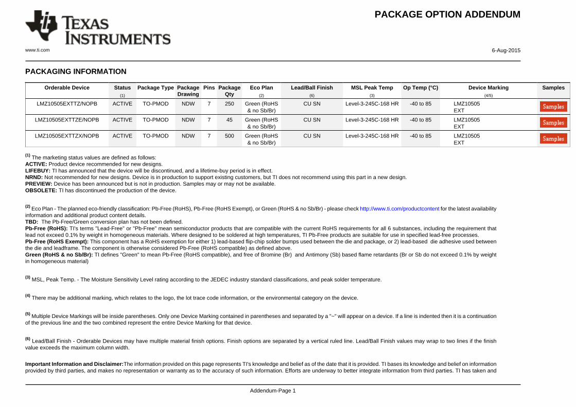
PACKAGING INFORMATION
Orderable Device Status(1)
Package Type PackageDrawing
Pins PackageQty
Eco Plan(2)
Lead/Ball Finish(6)
MSL Peak Temp(3)
Op Temp (°C) Device Marking(4/5)
Samples
LMZ10505EXTTZ/NOPB ACTIVE TO-PMOD NDW 7 250 Green (RoHS& no Sb/Br)
CU SN Level-3-245C-168 HR -40 to 85 LMZ10505EXT
LMZ10505EXTTZE/NOPB ACTIVE TO-PMOD NDW 7 45 Green (RoHS& no Sb/Br)
CU SN Level-3-245C-168 HR -40 to 85 LMZ10505EXT
LMZ10505EXTTZX/NOPB ACTIVE TO-PMOD NDW 7 500 Green (RoHS& no Sb/Br)
CU SN Level-3-245C-168 HR -40 to 85 LMZ10505EXT
(1) The marketing status values are defined as follows:ACTIVE: Product device recommended for new designs.LIFEBUY: TI has announced that the device will be discontinued, and a lifetime-buy period is in effect.NRND: Not recommended for new designs. Device is in production to support existing customers, but TI does not recommend using this part in a new design.PREVIEW: Device has been announced but is not in production. Samples may or may not be available.OBSOLETE: TI has discontinued the production of the device.
(2) Eco Plan - The planned eco-friendly classification: Pb-Free (RoHS), Pb-Free (RoHS Exempt), or Green (RoHS & no Sb/Br) - please check http://www.ti.com/productcontent for the latest availabilityinformation and additional product content details.TBD: The Pb-Free/Green conversion plan has not been defined.Pb-Free (RoHS): TI's terms "Lead-Free" or "Pb-Free" mean semiconductor products that are compatible with the current RoHS requirements for all 6 substances, including the requirement thatlead not exceed 0.1% by weight in homogeneous materials. Where designed to be soldered at high temperatures, TI Pb-Free products are suitable for use in specified lead-free processes.Pb-Free (RoHS Exempt): This component has a RoHS exemption for either 1) lead-based flip-chip solder bumps used between the die and package, or 2) lead-based die adhesive used betweenthe die and leadframe. The component is otherwise considered Pb-Free (RoHS compatible) as defined above.Green (RoHS & no Sb/Br): TI defines "Green" to mean Pb-Free (RoHS compatible), and free of Bromine (Br) and Antimony (Sb) based flame retardants (Br or Sb do not exceed 0.1% by weightin homogeneous material)
(3) MSL, Peak Temp. - The Moisture Sensitivity Level rating according to the JEDEC industry standard classifications, and peak solder temperature.
(4) There may be additional marking, which relates to the logo, the lot trace code information, or the environmental category on the device.
(5) Multiple Device Markings will be inside parentheses. Only one Device Marking contained in parentheses and separated by a "~" will appear on a device. If a line is indented then it is a continuationof the previous line and the two combined represent the entire Device Marking for that device.
(6) Lead/Ball Finish - Orderable Devices may have multiple material finish options. Finish options are separated by a vertical ruled line. Lead/Ball Finish values may wrap to two lines if the finishvalue exceeds the maximum column width.
Important Information and Disclaimer:The information provided on this page represents TI's knowledge and belief as of the date that it is provided. TI bases its knowledge and belief on informationprovided by third parties, and makes no representation or warranty as to the accuracy of such information. Efforts are underway to better integrate information from third parties. TI has taken and
PACKAGE OPTION ADDENDUM
www.ti.com 6-Aug-2015
Addendum-Page 2
continues to take reasonable steps to provide representative and accurate information but may not have conducted destructive testing or chemical analysis on incoming materials and chemicals.TI and TI suppliers consider certain information to be proprietary, and thus CAS numbers and other limited information may not be available for release.
In no event shall TI's liability arising out of such information exceed the total purchase price of the TI part(s) at issue in this document sold by TI to Customer on an annual basis.

TAPE AND REEL INFORMATION
*All dimensions are nominal
Device PackageType
PackageDrawing
Pins SPQ ReelDiameter
(mm)
ReelWidth
W1 (mm)
A0(mm)
B0(mm)
K0(mm)
P1(mm)
W(mm)
Pin1Quadrant
LMZ10505EXTTZ/NOPB TO-PMOD
NDW 7 250 330.0 24.4 10.6 14.22 5.0 16.0 24.0 Q2
LMZ10505EXTTZX/NOPB TO-PMOD
NDW 7 500 330.0 24.4 10.6 14.22 5.0 16.0 24.0 Q2
PACKAGE MATERIALS INFORMATION
www.ti.com 6-Aug-2015
Pack Materials-Page 1

*All dimensions are nominal
Device Package Type Package Drawing Pins SPQ Length (mm) Width (mm) Height (mm)
LMZ10505EXTTZ/NOPB TO-PMOD NDW 7 250 367.0 367.0 45.0
LMZ10505EXTTZX/NOPB TO-PMOD NDW 7 500 367.0 367.0 45.0
PACKAGE MATERIALS INFORMATION
www.ti.com 6-Aug-2015
Pack Materials-Page 2

MECHANICAL DATA
NDW0007A
www.ti.com
TZA07A (Rev D)
TOP SIDE OF PACKAGE
BOTTOM SIDE OF PACKAGE

IMPORTANT NOTICE
Texas Instruments Incorporated and its subsidiaries (TI) reserve the right to make corrections, enhancements, improvements and otherchanges to its semiconductor products and services per JESD46, latest issue, and to discontinue any product or service per JESD48, latestissue. Buyers should obtain the latest relevant information before placing orders and should verify that such information is current andcomplete. All semiconductor products (also referred to herein as “components”) are sold subject to TI’s terms and conditions of salesupplied at the time of order acknowledgment.TI warrants performance of its components to the specifications applicable at the time of sale, in accordance with the warranty in TI’s termsand conditions of sale of semiconductor products. Testing and other quality control techniques are used to the extent TI deems necessaryto support this warranty. Except where mandated by applicable law, testing of all parameters of each component is not necessarilyperformed.TI assumes no liability for applications assistance or the design of Buyers’ products. Buyers are responsible for their products andapplications using TI components. To minimize the risks associated with Buyers’ products and applications, Buyers should provideadequate design and operating safeguards.TI does not warrant or represent that any license, either express or implied, is granted under any patent right, copyright, mask work right, orother intellectual property right relating to any combination, machine, or process in which TI components or services are used. Informationpublished by TI regarding third-party products or services does not constitute a license to use such products or services or a warranty orendorsement thereof. Use of such information may require a license from a third party under the patents or other intellectual property of thethird party, or a license from TI under the patents or other intellectual property of TI.Reproduction of significant portions of TI information in TI data books or data sheets is permissible only if reproduction is without alterationand is accompanied by all associated warranties, conditions, limitations, and notices. TI is not responsible or liable for such altereddocumentation. Information of third parties may be subject to additional restrictions.Resale of TI components or services with statements different from or beyond the parameters stated by TI for that component or servicevoids all express and any implied warranties for the associated TI component or service and is an unfair and deceptive business practice.TI is not responsible or liable for any such statements.Buyer acknowledges and agrees that it is solely responsible for compliance with all legal, regulatory and safety-related requirementsconcerning its products, and any use of TI components in its applications, notwithstanding any applications-related information or supportthat may be provided by TI. Buyer represents and agrees that it has all the necessary expertise to create and implement safeguards whichanticipate dangerous consequences of failures, monitor failures and their consequences, lessen the likelihood of failures that might causeharm and take appropriate remedial actions. Buyer will fully indemnify TI and its representatives against any damages arising out of the useof any TI components in safety-critical applications.In some cases, TI components may be promoted specifically to facilitate safety-related applications. With such components, TI’s goal is tohelp enable customers to design and create their own end-product solutions that meet applicable functional safety standards andrequirements. Nonetheless, such components are subject to these terms.No TI components are authorized for use in FDA Class III (or similar life-critical medical equipment) unless authorized officers of the partieshave executed a special agreement specifically governing such use.Only those TI components which TI has specifically designated as military grade or “enhanced plastic” are designed and intended for use inmilitary/aerospace applications or environments. Buyer acknowledges and agrees that any military or aerospace use of TI componentswhich have not been so designated is solely at the Buyer's risk, and that Buyer is solely responsible for compliance with all legal andregulatory requirements in connection with such use.TI has specifically designated certain components as meeting ISO/TS16949 requirements, mainly for automotive use. In any case of use ofnon-designated products, TI will not be responsible for any failure to meet ISO/TS16949.
Products ApplicationsAudio www.ti.com/audio Automotive and Transportation www.ti.com/automotiveAmplifiers amplifier.ti.com Communications and Telecom www.ti.com/communicationsData Converters dataconverter.ti.com Computers and Peripherals www.ti.com/computersDLP® Products www.dlp.com Consumer Electronics www.ti.com/consumer-appsDSP dsp.ti.com Energy and Lighting www.ti.com/energyClocks and Timers www.ti.com/clocks Industrial www.ti.com/industrialInterface interface.ti.com Medical www.ti.com/medicalLogic logic.ti.com Security www.ti.com/securityPower Mgmt power.ti.com Space, Avionics and Defense www.ti.com/space-avionics-defenseMicrocontrollers microcontroller.ti.com Video and Imaging www.ti.com/videoRFID www.ti-rfid.comOMAP Applications Processors www.ti.com/omap TI E2E Community e2e.ti.comWireless Connectivity www.ti.com/wirelessconnectivity
Mailing Address: Texas Instruments, Post Office Box 655303, Dallas, Texas 75265Copyright © 2015, Texas Instruments Incorporated