Power Minimization Of10tfull Adder Using Sub ... · The full adder designs are simulated by Tanner...
13
ADVANCES in NATURAL and APPLIED SCIENCES ISSN: 1995-0772 Published BY AENSI Publication EISSN: 1998-1090 http://www.aensiweb.com/ANAS 2016 Special 10(14): pages 127-139 Open Access Journal To Cite This Article: C. Thiripurasundari, Dr.V.Sumathy, C. Thiruvengadam., Power Minimization Of10tfull Adder Using Sub-Microntechnique & Pfalfull Adder Usingadiabatic Logic. Advances in Natural and Applied Sciences. 10(14); Pages: 127- 139 Power Minimization Of10tfull Adder Using Sub-Microntechnique & Pfalfull Adder Usingadiabatic Logic 1 C. Thiripurasundari, 2 Dr.V.Sumathy, 3 C. Thiruvengadam 1 Assistant Professor, ECE Department, M.E.C., Anna university, Chennai, Tamil Nadu, India. 2 Associate Professor, ECE Department, G.C.T.,Coimbatore-641013, Tamil Nadu, India. 3 Assistant Professor, ECE Department, AAMEC, Anna university, Chennai, Tamil Nadu, India. Received 7 June 2016; Accepted 12 October 2016; Available 20 October 2016 Address For Correspondence: C. Thiripurasundari, Assistant Professor, ECE Department, M.E.C., Anna university, Chennai, Tamil Nadu, India E-mail: [email protected] Copyright © 2016 by authors and American-Eurasian Network for Scientific Information (AENSI Publication). This work is licensed under the Creative Commons Attribution International License (CC BY). http://creativecommons.org/licenses/by/4.0/ ABSTRACT Due to the demand for low PowerPC’s, 10TFullAdderusingsub-micron technique and Positive Feedback Adiabatic Logic (PFAL) Full Adder using adiabatic logic are designed to reduce the power consumption. The full adder designs are simulated by Tanner tool. 10T full adder works under the sub-micron technique. Using 10T full adder, the power consumption and area can be reduced. Because the 10T full adder requires only 10 numbers of transistors. Since the adiabatic logic is used in PFAL full adder, it reuses the leakage power. so the leakage power is less because only pros transistors reused, it avoids the ground connection. The power consumption results of existing and proposed systems are compared. KEYWORDS: Keyword1 :Adiabatic Logic Keyword 2 : Sub-micron Keyword 3 : Leakage Power INTRODUCTION Ever increasing demand for low power ICs in digital measurement instrumentation, palm top computers, cellular mobile, etc., makes us to consider low power features of IC’s along with other circuit features. Speed- limiting elements of microprocessors and DSPs are the arithmetic cooperation used. During the design of an adder, different design abstraction levels are considered. One is liable for the adder’s architecture implemented with the one-bit full adder as a building block. The other defines the specific propose sty leapt transistor level to implement the one-bit full adder. 1.1basic Functionof Adder: In digital electronics, an adder is a digital circuit that performs addition of numbers. In many computer and other kinds of processors, adders are used not only in the arithmetic logic unit(s), but also in other parts of the processor, where they are used to calculate addresses, table indices, etc. Although adders can be constructed for many numerical representations, such as binary-coded decimalorexcess-3, the most common adders operate on binary numbers. In cases where two’s complement or one’s complement is being used to represent negative numbers, it is trivial to modify an adder into a 2%adder-subtractor. Other signed number representations require a more complex adder.
-
Upload
hoangtuong -
Category
Documents
-
view
227 -
download
4
Transcript of Power Minimization Of10tfull Adder Using Sub ... · The full adder designs are simulated by Tanner...
ADVANCES in NATURAL and APPLIED SCIENCES
ISSN: 1995-0772 Published BY AENSI Publication
EISSN: 1998-1090 http://www.aensiweb.com/ANAS
2016 Special 10(14): pages 127-139 Open Access Journal
To Cite This Article: C. Thiripurasundari, Dr.V.Sumathy, C. Thiruvengadam., Power Minimization Of10tfull Adder Using Sub-Microntechnique & Pfalfull Adder Usingadiabatic Logic. Advances in Natural and Applied Sciences. 10(14); Pages: 127-
139
Power Minimization Of10tfull Adder Using
Sub-Microntechnique & Pfalfull Adder
Usingadiabatic Logic
1C. Thiripurasundari, 2Dr.V.Sumathy, 3C. Thiruvengadam
1Assistant Professor, ECE Department, M.E.C., Anna university, Chennai, Tamil Nadu, India. 2Associate Professor, ECE Department, G.C.T.,Coimbatore-641013, Tamil Nadu, India. 3Assistant Professor, ECE Department, AAMEC, Anna university, Chennai, Tamil Nadu, India.
Received 7 June 2016; Accepted 12 October 2016; Available 20 October 2016
Address For Correspondence:
C. Thiripurasundari, Assistant Professor, ECE Department, M.E.C., Anna university, Chennai, Tamil Nadu, India
E-mail: [email protected]
Copyright © 2016 by authors and American-Eurasian Network for Scientific Information (AENSI Publication).
This work is licensed under the Creative Commons Attribution International License (CC BY).
http://creativecommons.org/licenses/by/4.0/
ABSTRACT Due to the demand for low PowerPC’s, 10TFullAdderusingsub-micron technique and Positive Feedback Adiabatic Logic (PFAL) Full
Adder using adiabatic logic are designed to reduce the power consumption. The full adder designs are simulated by Tanner tool.
10T full adder works under the sub-micron technique. Using 10T full adder, the power consumption and area can be reduced.
Because the 10T full adder requires only 10 numbers of transistors. Since the adiabatic logic is used in PFAL full adder, it reuses the
leakage power. so the leakage power is less because only pros transistors reused, it avoids the ground connection. The power
consumption results of existing and proposed systems are compared.
KEYWORDS: Keyword1 :Adiabatic Logic Keyword 2 : Sub-micron Keyword 3 : Leakage Power
INTRODUCTION
Ever increasing demand for low power ICs in digital measurement instrumentation, palm top computers, cellular mobile, etc., makes us to consider low power features of IC’s along with other circuit features. Speed-limiting elements of microprocessors and DSPs are the arithmetic cooperation used. During the design of an adder, different design abstraction levels are considered. One is liable for the adder’s architecture implemented with the one-bit full adder as a building block. The other defines the specific propose sty leapt transistor level to implement the one-bit full adder.
1.1basic Functionof Adder:
In digital electronics, an adder is a digital circuit that performs addition of numbers. In many computer and other kinds of processors, adders are used not only in the arithmetic logic unit(s), but also in other parts of the processor, where they are used to calculate addresses, table indices, etc. Although adders can be constructed for many numerical representations, such as binary-coded decimalorexcess-3, the most common adders operate on binary numbers. In cases where two’s complement or one’s complement is being used to represent negative numbers, it is trivial to modify an adder into a 2%adder-subtractor. Other signed number representations require a more complex adder.

128 C. Thiripurasundari et al., 2016/ Advances in Natural and Applied Sciences. 10(14) Special 2016, Pages: 127-139
Fig. 1: Half Adder Logic Diagram
The half adder adds two one-bit binary numbers A and B. It has two outputs, Sand C. The simplest half-
adder design incorporate an XOR gate for Sandman AND gateforCasshowninFig1. With the addition of an OR gate to combine their carry outputs, two half adders can be combined to make a full adder. The below equationsatisfiesthetruthtable1
Sum= A^B, Carry= A&B
Table 1: Truth Table for Half Adder
Fig. 2: Full Adder Logic Diagram
A full adder can be implemented in many different ways such a switch a custom transistor-level circuit or
composed of other gates. One example implementation is with Sand Court. In this implementation, the final OR gate before the carry-out output may be replaced by an XOR gate without altering the result in logic. A full adder can be constructed from two half adders by connecting A and B to the input of one half adder, connecting the sum from that to an input to the second adder, connecting Ci to the other input and OR the two carry out put sash owning Fig2.Equivalently, Should be made the three-bit XOR of A, B, and Ci, and Cout could be made the three-bit majority function of A, B, and Ci.
Table 2: Truth Table for Full Adder
1.2 Differenttypesofadders: (A) Ripple-carry adder:

129 C. Thiripurasundari et al., 2016/ Advances in Natural and Applied Sciences. 10(14) Special 2016, Pages: 127-139
Fig 3: 4 Bit Ripple Carry Adders
It is possible to create logical circuit using multiple full adders to add N-bit numbers. Each full adder input
sac in, which is the court of the previous adder. This kind of adder is called a ripple-carry adder, since each carry bit "ripples" to the next full adder as shown in above Fig.3. The ripple-carry adder is relatively slow; each full adder must wait for the carry bit to be calculated from the previous full adder. The gate delay can easily be calculated by inspection of the full adder circuit.
(B) Carry-look ahead adders:
Fig. 4: 4 Bit Carry-look ahead adder To reduce the computation time, engineers devised faster ways to add two binary numbers by using carry-
look ahead adder. They work by creating two signals (Pang) for each bit position, based on if a carry is prop gated through from a less significant bit position(atleastoneinputisa'1'), a carry is generated in that bit position(bothinputsare'1'), or if a carry is killed in that bit position (bothinputsare'0'). Some other multi-bit adder architectures break the adder into blocks. It is possible to vary the length of these blocks based on the propagation delay of the circuits to optimize computation time. These block based adders include the carry by pass adder, which will determine P and G values for each blockratherthaneachbit and thecarryselectadderwhichpre-generatessum and carry values for either possible carry input to the block shown in Fig. 4.
Existingsystem:
Different types of CMOS design are consideration for reduction of power and area. The main purpose of this FA is to introduce an essential component to binary computation-a full adder. In this paper the comparison of different types of full adder circuits were done. The e x i s t i n g 5different types of full adder circuits are l i s t e d a n d a r e simulated by the Tanner EDA tools.
1. Conventional CMOS Full Adder 2. Mirror adder 3. CPL Full adder 4. LEAP Adder 5. SERF full adder
2.1 Conventional CMOS full adder: Conventional CMOS Implementation consists of two functional blocks pull-up and pull-down. Pull-up
functional block is implemented with P-channel MOS transistors and pull down functional block is implemented with N-channel MOS transistors. In order to get symmetrical structure, blocks are, rearranged as and sum and carry implementation is shown in F i g . 5 . The1-bit full adder has 14p MOS and 14n MOS transistor. The CMOS structure combines sp Mosul-up and n MOS pull-down networks. In this style all transistors (either p

130 C. Thiripurasundari et al., 2016/ Advances in Natural and Applied Sciences. 10(14) Special 2016, Pages: 127-139
MOS or n MOS) are arranged in completely separate branches, each may consist of several sub-branches [1 2].
Fig. 5: Conventional CMOS full adder
2.2Mirror adder: Then n MOS and p MOS chains are completely symmetrical w i t h ea c h o t he r as shown in the Fig6. A
maximum of two series transistors can be observed in the carry-generation circuitry. When laying out the cell, the most critical issue is the minimization of the capacitance at node C0. There reduction of the diffusion capacitances is particularly important. The capacitance at node C0 is composed of four diffusion capacitances, two in thermal gate capacitances, and gate capacitances in the connecting adder cell. The transistors connected to C in are placed closest to the output. Only the transistors in the carry stage have to be optimized for optimal speed. All transistors in the sum stage can be minimal size [2].
Fig. 6: Mirror adder 2.3. CPL Full adder:
The Fig. 7 shows the CPL Adder circuit diagram. The CPL adder circuit is the best performing pass transistor logic and in particular, the fastest one. CPL proves to have the best performance values and lowest power delay products.CPL version with down sized transistor still consumes twice as much power and is slower than CMOS. It has greater powered is sedation. In CPL Full adder SUM there are 4pMOS and 10 n MOS are used and for CARRY there are 4pMOSand12nMOSareused.
Fig. 7: CPLFulladder

131 C. Thiripurasundari et al., 2016/ Advances in Natural and Applied Sciences. 10(14) Special 2016, Pages: 127-139
2.4leapadder: The circuit diagram for LEAP Adder as shown in Fig8 is quite power efficient but rather slow. LEAP
Adder does not workat1.5Vandits superiority over COMS at high Voltages could not be confirmed. It is viable alternative if lower power and compatibility with cell based design are of concern. LEAP Adder in order to better exploit the multiplexer structure of pass transistor logic referred in [3].
Fig. 8: Leap adder 2.5TFAfull adder:
The transmission function full adder, which uses 16 transistors for the realization of the circuit, is shown in Fig. 9 for this circuit there are two possible short-circuit paths to ground. This design uses both pull-up and pull- down logic as well as complementary pass logic to drive the load. The TFA is also based in the transmission function theory. It uses pull-up and pull-down paths to makes the inverters. In this circuit there are four pass transistors used [4]. The main disadvantage of T FA is the lack of the driven capacity, suffering more signal degradation when case added. TFA adder present low power consumption for the nominal voltage.
Fig. 9: TFA Full Adder
The setbacks of the existing systems are,
i. High power consumption. ii. The conventional CMOS full adder and Mirror adder reconstructed by using 28 transistors. So, they
require more area. iii. In CPL and LEAP full adders required separate circuit connection for sum and carry output. iv. In TFA, lack of the driven capacity, suffering more signal degradation when cascaded.
3. Proposed System:
In this work two types of full adder circuits design are proposed to minimize the power consumption. A comparison various parameter like, the minimum, maximum and average power consumption are done with the existing full adder’s circuits and with the proposed model. The proposed full adder circuits are, i) 10TFullAdder ii) PFAL Full Adder
3.1.10t Full Adder:
The power minimization of 10T full adders one by using sub-micron technique. 10T indicates 10CMOS transistor search 5CMOS transistor sere grouped to form a half adder circuit. So, it will avoid more area. The 10T Adder circuit of 10T Adders one-bit has three inputs (A, B, and C in) outputs (sum S and carry out Co). The made of five CMOS inverters that are shown. Input A is directly connected to inverter first while input B is connected second and third inverter. Second inverter p MOS and inverter n MOS drain a reconnected first inverter output while second inverter n MOS inverter drain are connected directly input A. The Second inverter output is connected fourth inverter in put Ci is given in inverter fifth. There is interesting, the power supply VDD connected first inverter only. All transistors have minimum length according to used Technology, while

132 C. Thiripurasundari et al., 2016/ Advances in Natural and Applied Sciences. 10(14) Special 2016, Pages: 127-139
typically design parameters. The proposed full adder is proven to have the minimum power consumption and less power-delay product by Tanner simulation comparing with other prior literature, the characteristics of the novel hybrid full adder shows that the design has the best power-delay product for carry out signal.
In10T full adder circuit (Fig. 10) number of CMOS transistor are less compare to the existing full adder circuits. So we can reduce the area of the full adder circuit. The power consumption of 10CMOS transistors are less, because in the above 5 existing system they were used28,30,20etc,.So using10Tfulladders we can reduce the power consumption and leakage of power
Fig. 10: 10T FULL ADDER
3.2positive Feedback Adiabaticlogic (PFAL): PFAL, like IECRL, is also based around a pair of cross coupled inverters. However, in IECRL then MOS
devices used to evaluate the function are connected between the output sand ground, in PFAL, these evaluation n MOS devices are connected between the output sand the power-Clock. The similarities between PFAL and IECRL gates are such that IECRL gates can be easily converted into PFAL gates. This is done by re-labelling the outputs so that their assertion level sere swapped, and connecting then MOS evaluation devices between the power-clock and the outputs rather than between ground and the outputs. This can be made as easy to achieve in layout as it is in abstract representation of the circuit.
Logical Operation of PFAL:
The PFAL stands for the Positive Feedback A diabetic Logic. It is a dual rail diabetic circuit capable of realizing partial energy recovery. Analogous to the 2N2N-2P logic, this logical the four-phase power-clock, consisting of 4phases, namely, [3 4]
(1) The rising phase of power-clock called evaluate, (2)The constant phase called hold, when the output is held for the next stage to evaluate this signal, (3) The falling phase of power-clock called reset or recovery, (4) Where the process of charge reclamation or charge retrieval takes place. This is followed by the Wait phase, which synchronizes the flow of data across the a diabetic pipe line. The
heart of the PFAL circuits is the diabetic amplifier latch made by two p MOS and n MOS transistors. The main difference between the PFAL and the 2N2N-2P logics is that the complementary functional blocks in PFAL are implemented as a pull-up network, in parallel with the two p MOS devices. This has its characteristic advantages and disadvantages, when compared to the 2N2N-2P logic. The evaluate phase of the power-clock, assume that then put X is already high and X low. When the power-clock voltage level rises above the threshold voltage of then MOS transistor, the transistor MX conducts and connects theorising node voltage Y to power clock. This node Y with rising voltage turns on the device MN2 and pulls the node /Y to ground. This in turn is applied to the gate of the pMOSdeviceMP1.ThisineffectrealizesaparallelcombinationofthepMOS and n MOS devices, namely, MX and MP1. This results in reduced ON resistance through the transmission gate structure. This reduction of resistance is the main advantage of the PFAL.

133 C. Thiripurasundari et al., 2016/ Advances in Natural and Applied Sciences. 10(14) Special 2016, Pages: 127-139
Fig. 11: PFAL Full Adder
Features of PFAL: During their cover phase, the power-clock voltage reduces. Then, due to the potential difference existing
between the power rail and Y node, the charge gets transfer red back to the PC. However, since the input n MOS device at this time is OFF, energy recovery is made possible only through the p MOS device. This in effect poses increased resistance. When the PC voltage is lower than the Vth of the p MOS device, the charge recovery stops. This results in the floating node problem, due to the remnant charge. This remaining charge is retained in the output node and is dissipated in the next stage, when the states of the diabetic stage change. Hence, this logic falls under quasi a diabetic family, that is complete recovery of energy is not possible due to the losses mentioned above. The floating output node problem also results in poorer high frequency performance. A diabetic circuit sere usually designed with methodologies optimized for the application in which they are used. In this work we show how a conventional design-flow based on and an adiabatic standard-cell library and semiautomatic tools allow the quick and easy design and verification of a complex an adiabatic system, without losing the energy reduction benefits.
The methodology has been applied to the design of positive feedback adiabatic logic (PFAL) carry look-ahead adders (CLA).
Post-layout simulations of the standard- cell PFAL Class show a 94% energy recovery as compared to a conventional static CMOSCLA at 10MHz, and 86% at 100MHz. The standard-cell PFAL CLAs are also more energy efficient or comparable than other custom adiabatic CLAs found in the literature. 4. Simulation Results: 4.1. Simulstion Results For Existing System: Conventional Full Adder:
Fig. 12: Simulation Result for Conventional Full Adder
The above wave form represents the performance of conventional CMOS full adder. In the Fig. 12a,b,c
represent the input wave form sum and carry are representing the output wave form. The above waveform satisfy the truth table for full adder circuit shown in the table 2

134 C. Thiripurasundari et al., 2016/ Advances in Natural and Applied Sciences. 10(14) Special 2016, Pages: 127-139
Fig. 13: Power Report for Conventional Full Adder The above power analysis report snap shot shows the minimum power consumption, maximum power
consumption and average power consumption for conventional CMOS full adder circuits.
Mirror Adder: The given wave forms are the input and output waveform forth mirror adder. The three inputs area, b, c.
The two outputs are sum and carry. This waveform satisfy the truth table for full adder shown in above table 1.2
Fig. 14: Simulation Result for Mirror Adder
Fig. 15: Power Report for Mirror Adder
The above power analysis report snapshot shows the minimum power consumption, maximum power
consumption and average power consumption for mirror adder circuits.

135 C. Thiripurasundari et al., 2016/ Advances in Natural and Applied Sciences. 10(14) Special 2016, Pages: 127-139
CPL Full Adder:
Fig. 16: Simulation Result for CPL Full Adder The above wave form represents the performance of CPL full adder. Int he above figure a, b, c represent the
input wave form sum and carry are representing the output wave form. This above wave form satisfy the truth table for full adder circuit shown in the table 1.2
Fig. 17: Power Report for CPL Full Adder
The above power analysis report snap shot shows the minimum power consumption, maximum power
consumption and average power consumption for CPL full adder circuits Simulation Result for LEAP Full Adder:
The given wave form sere the input and output wave form for the LEAP full adder. The three input sere a, b, c. The two output saris and carry. This wave form satisfy the truth table for full adder shown in above table 1.2
Fig. 18: Simulation Result for LEAP Full Adder

136 C. Thiripurasundari et al., 2016/ Advances in Natural and Applied Sciences. 10(14) Special 2016, Pages: 127-139
Power Report for LEAP Full Adder:
Fig. 19: Power Report for LEAP Full Adder The above power analysis report snapshot shows the minimum power consumption, maximum power
consumption and average power consumption for LEAP full adder circuits. TFA Full Adder:
The wave form represents the performance of TFA full adder. In the above figure a, b, c represent the input wave form sum and carry are representing the output wave form. This above wave form satisfies the truth table for full adder circuit.
Fig. 20: Simulation Result for TFA Full Adder
Power Report for TFA Full Adder:

137 C. Thiripurasundari et al., 2016/ Advances in Natural and Applied Sciences. 10(14) Special 2016, Pages: 127-139
Fig. 21: Power Report for TFA Full Adder
The above power analysis report snapshot shows the minimum power consumption, maximum power
consumption and average power consumption for TFA full adder circuits.
4.2 Simulstionresults Forproposedsystems10t Full Adder:
Fig. 22: Simulation Result for 10TFullAdder The given wave forms are the input and out put wave form for the 10T full adder. The three inputs area, b,
c. The two outputs are sum and carry. These wave forms in truth table for full adder shown in above table 1.2
Power Report for 10T Full Adder: The power analysis report shows the minimum power consumption, maximum power consumption and
average power consumption for conventional 10Tfull adder circuits.

138 C. Thiripurasundari et al., 2016/ Advances in Natural and Applied Sciences. 10(14) Special 2016, Pages: 127-139
Fig. 23: Power Report for 10T Full Adder
PFAL Full Adder: The given wave forms are the input and output wave form for the PFL full adder. The three inputs are a, b,
c. The two outputs are sum and carry. This wave form satisfy the truth table for full adder shown in above table 2
Fig. 24: Simulation Result for 10TFullAdder
Power Report of PFAL Full Adder:
The power analyse is report shows the minimum power consumption, maximum power consumption and average power consumption for conventional PFAL full adder circuits
Fig. 25: Power Report of PFAL Full Adder
139 C. Thiripurasundari et al., 2016/ Advances in Natural and Applied Sciences. 10(14) Special 2016, Pages: 127-139
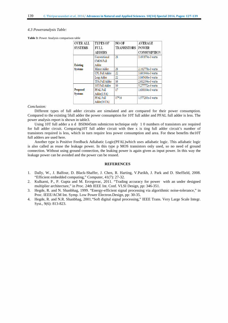
4.3 Poweranalysis Table:
Table 3: Power Analysis comparison table
Conclusion:
Different types of full adder circuits are simulated and are compared for their power consumption. Compared to the existing 5full adder the power consumption for 10T full adder and PFAL full adder is less. The power analysis report is shown in table3.
Using 10T full adder a n d BSIM45nm submicron technique only 1 0 numbers of transistors are required for full adder circuit. Comparing10T full adder circuit with thee x is ting full adder circuit’s number of transistors required is less, which in turn require less power consumption and area. For these benefits the10T full adders are used here.
Another type is Positive Feedback Adiabatic Logic(PFAL)which uses adiabatic logic. This adiabatic logic is also called as reuse the leakage power. In this type p MOS transistors only used, so no need of ground connection. Without using ground connection, the leaking power is again given as input power. In this way the leakage power can be avoided and the power can be reused.
REFERENCES
1. Dally, W., J. Balfour, D. Black-Shaffer, J. Chen, R. Harting, V.Parikh, J. Park and D. Sheffield, 2008.
“Efficient embedded computing,” Computer, 41(7): 27-32. 2. Kulkarni, P., P. Gupta and M. Ercegovac, 2011. “Trading accuracy for power with an under designed
multiplier architecture,” in Proc. 24th IEEE Int. Conf. VLSI Design, pp: 346-351. 3. Hegde, R. and N. Shanbhag, 1999. “Energy-efficient signal processing via algorithmic noise-tolerance,” in
Proc. IEEE/ACM Int. Symp. Low Power Electron.Design, pp: 30-35. 4. Hegde, R. and N.R. Shanbhag, 2001.“Soft digital signal processing,” IEEE Trans. Very Large Scale Integr.
Syst., 9(6): 813-823.