

Power Electronics & Electric Machinery Innovations at … Library/Research/Coal/energy...
72
Power Electronics & Electric Machinery Innovations at Oak Ridge National Laboratory Don Adams SECA Core Technology Program Review June 19, 2002
Transcript of Power Electronics & Electric Machinery Innovations at … Library/Research/Coal/energy...

Power Electronics & Electric Machinery
Innovations at Oak Ridge National Laboratory
Don AdamsSECA Core Technology Program Review
June 19, 2002

Unique: Power Electronics & Electric Machinery Research Center
• A staff of 20 researchers • 700 m2 laboratories • Only DOE national laboratory with an
all-encompassing PEEM program.• The Center’s world-wide reputation is
supported by awards, patents, publications, and recognition by professional societies, academia, industry and DOE.
100 kW, installed on vehicle 1999Soft switching and sensorless
Rotor of a HSUB motor
Stator armature of a HSUB motor
Stator DC field end bracket
• The Center is actively involved in partnerships with several universities, private and public companies, other federal agencies, and consortiums.• Projects supported by various offices of DOE, DOD, and industry.• Plurality of funding is for hybrid-electric vehicles, and other areas include heavy hybrid vehicles, fuel cells, distributed energy, power quality and transmission, and motors and drives for special applications.• Projects directly funded by industrial partners allow proprietary work.
Government R&D Programs
• Power Electronics & Motors Pervade Almost All GovernmentR&D Programs
• Developments Are Synergistic and Useful to All• Each Application Has Specific Requirements
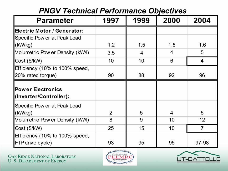
Parameter 1997 1999 2000 2004Electric Motor / Generator:Specif ic Pow er at Peak Load (kW/kg) 1.2 1.5 1.5 1.6Volumetric Pow er Density (kW/l) 3.5 4 4 5Cost ($/kW) 10 10 6 4Efficiency (10% to 100% speed, 20% rated torque) 90 88 92 96
Power Electronics (Inverter/Controller):
Specif ic Pow er at Peak Load (kW/kg) 2 5 4 5Volumetric Pow er Density (kW/l) 8 9 10 12Cost ($/kW) 25 15 10 7Efficiency (10% to 100% speed, FTP drive cycle) 93 95 95 97-98
PNGV Technical Performance Objectives
• Integrate commonly used power electronics into single inverter package
• Increase automotive energy efficiency• Reduce component costs
DOE/FreedomCAR AIPM ProjectDOE/FreedomCAR AIPM Project
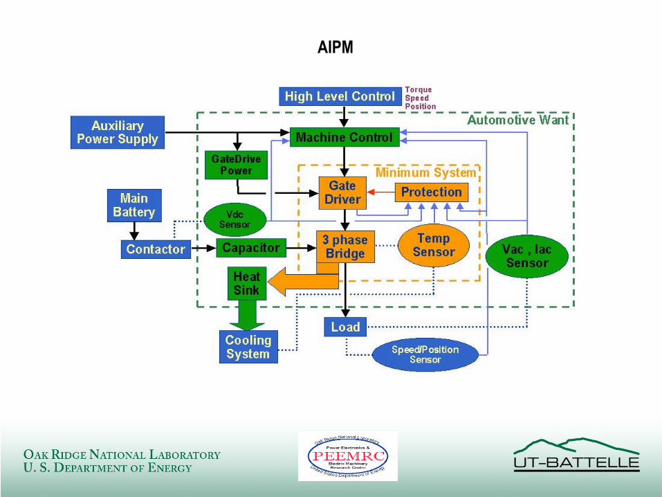
AIPM
AIPM
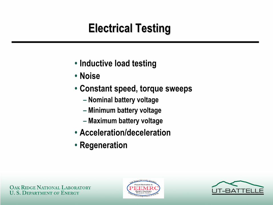
Electrical TestingElectrical Testing
• Inductive load testing • Noise• Constant speed, torque sweeps
– Nominal battery voltage– Minimum battery voltage– Maximum battery voltage
• Acceleration/deceleration• Regeneration
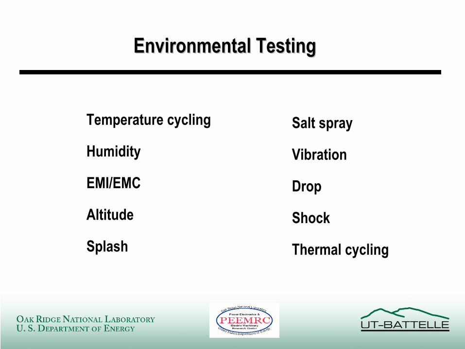
Environmental TestingEnvironmental Testing
Temperature cycling
Humidity
EMI/EMC
Altitude
Splash
Salt spray
Vibration
Drop
Shock
Thermal cycling
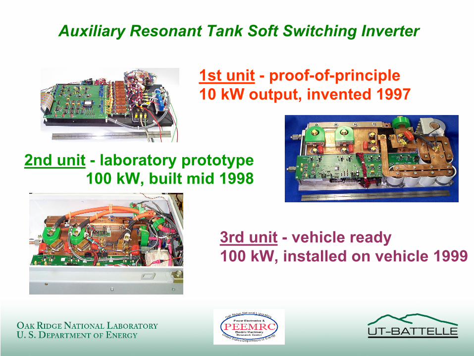
1st unit - proof-of-principle10 kW output, invented 1997
2nd unit - laboratory prototype100 kW, built mid 1998
3rd unit - vehicle ready100 kW, installed on vehicle 1999
Auxiliary Resonant Tank Soft Switching Inverter
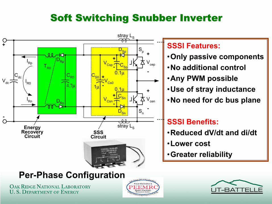
Soft SwitchingSoft Switching SnubberSnubber InverterInverter
SSSI Features:•Only passive components•No additional control•Any PWM possible•Use of stray inductance •No need for dc bus plane
SSSI Benefits:•Reduced dV/dt and di/dt•Lower cost•Greater reliability
Per-Phase Configuration
+
-
stray LS
stray LS
0.1µ
0.1µ4.7µ
SSSCircuit
EnergyRecovery
Circuit
+
-
Vcep
+
-
Vcen
IRp
IRn
Vdc1µ
DSp
DSn
CSn
CSp
CS0
TR0
CR0
Sp
Sn
DRp
DRn
CdcIR0
+
+
+
-
-
-
VCsp
VCsn
VCs0
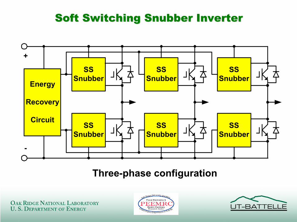
Soft SwitchingSoft Switching SnubberSnubber InverterInverter
SSSnubber
SSSnubber
+
-
SSSnubber
SSSnubber
SSSnubber
SSSnubber
Energy
Recovery
Circuit
Three-phase configuration
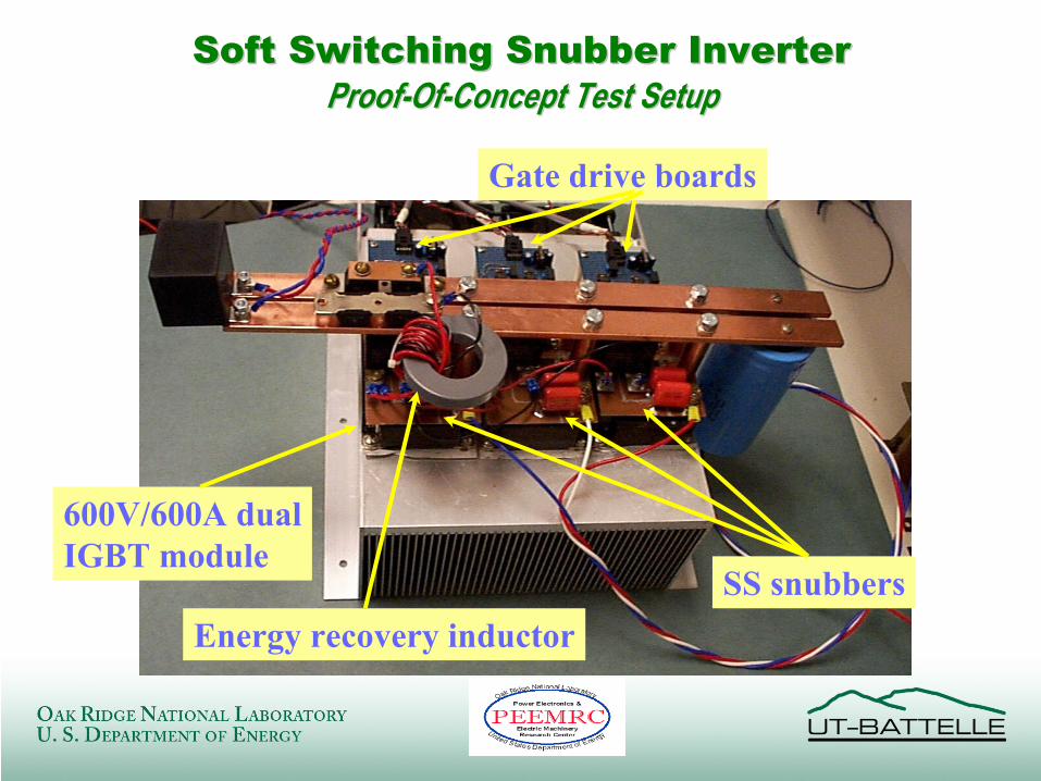
Soft SwitchingSoft Switching SnubberSnubber InverterInverterProofProof--OfOf--Concept Test SetupConcept Test Setup
Energy recovery inductorSS snubbers
Gate drive boards
600V/600A dualIGBT module
- Background Review -• Challenges in DC/DC Converters for Fuel Cell Vehicles
– High power and high current – 5 kW peak/1.6 kW cont. – High voltage ratio – 12 V vs 300 V– Bi-directional– Low cost and reliability– Very few topologies/products available
• High cost, excessive number of components• High EMI emission
• DC/DC Converter Development at ORNL– First generation (1997~1999, developed at Virginia Tech
through subcontract)– Second generation (1999~)
BiBi--directional DC/DC Converterdirectional DC/DC Converter

BiBi--directional DC/DC Converterdirectional DC/DC Converter
– Dual full bridges– Soft switching with the help
of the clamping circuit
Vin
Ldc
+
1:n
-
Id1
Vr1 Vr2
Cr1
Cr2
Cr3
Cr4
C1
C2
C3
C4
V1
V2
V3
V4
S1
S2
S3
S4
D1
D2
D3
D4
Ir1Vout
LoadVin
Ldc
LowVoltageDC Bus
Vout
ClampingCircuit
LowVoltageBridge
HighVoltageBridge
Transformer
HighVoltageDC Bus
– Half the component count– Soft switching w/o
additional components– Less control and
accessories (power supplies, gate drivers)
– More compact, light, and reliable
– Low cost
First Generation
Second Generation
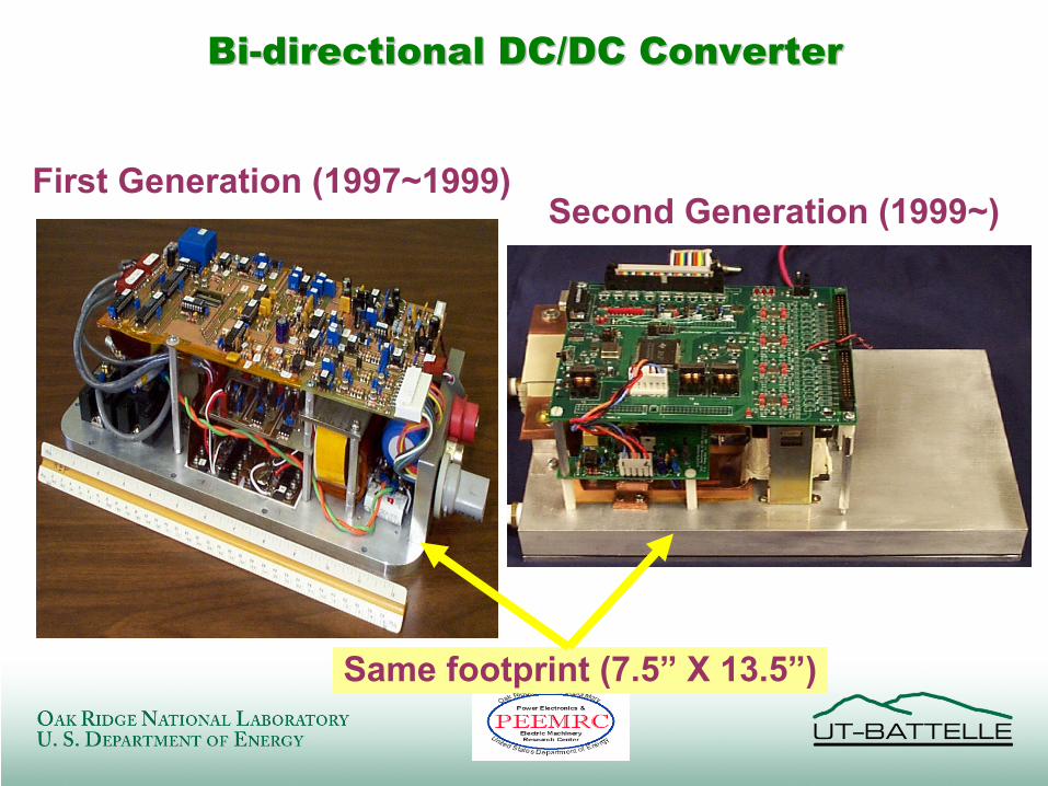
BiBi--directional DC/DC Converterdirectional DC/DC Converter
First Generation (1997~1999)Second Generation (1999~)
Same footprint (7.5” X 13.5”)
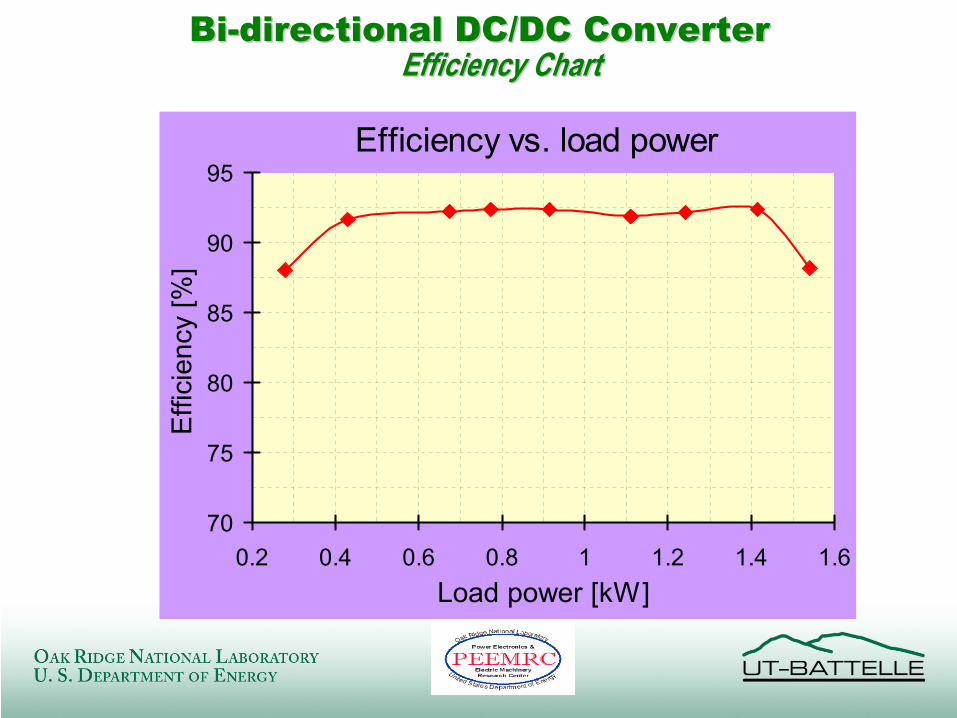
BiBi--directional DC/DC Converterdirectional DC/DC ConverterEfficiency ChartEfficiency Chart
Efficiency vs. load power
70
75
80
85
90
95
0.2 0.4 0.6 0.8 1 1.2 1.4 1.6Load power [kW]
Effic
ienc
y [%
]
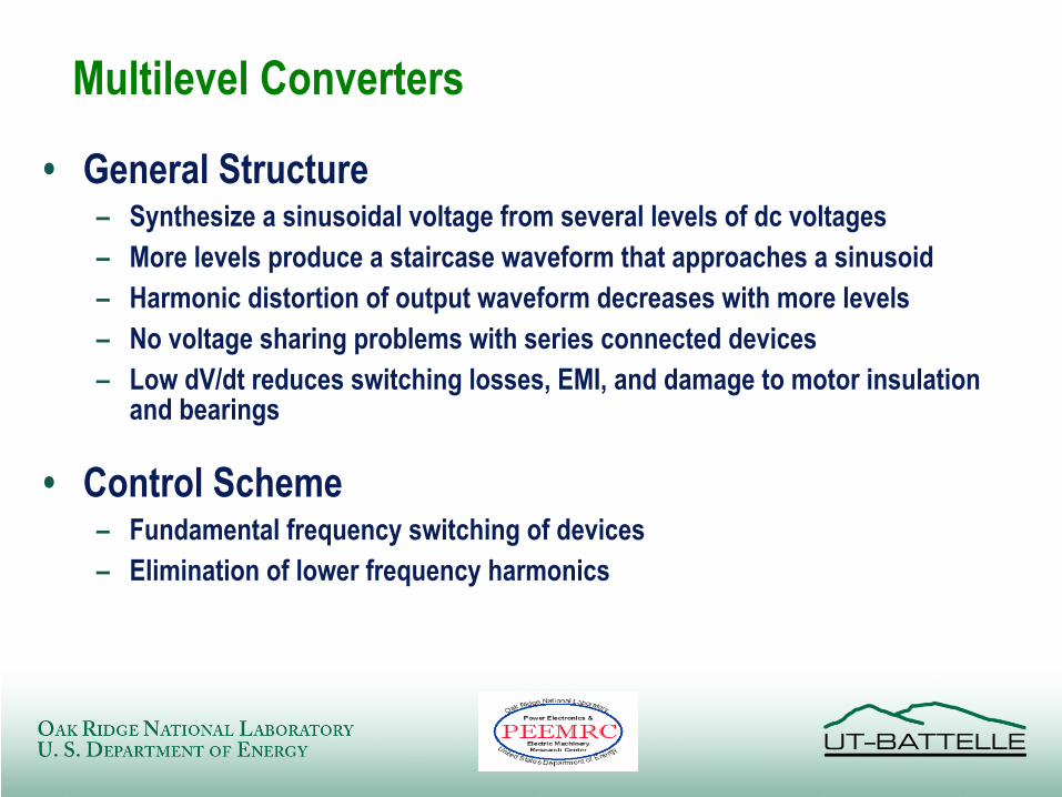
Multilevel Converters
• General Structure– Synthesize a sinusoidal voltage from several levels of dc voltages– More levels produce a staircase waveform that approaches a sinusoid– Harmonic distortion of output waveform decreases with more levels– No voltage sharing problems with series connected devices– Low dV/dt reduces switching losses, EMI, and damage to motor insulation
and bearings
• Control Scheme– Fundamental frequency switching of devices– Elimination of lower frequency harmonics
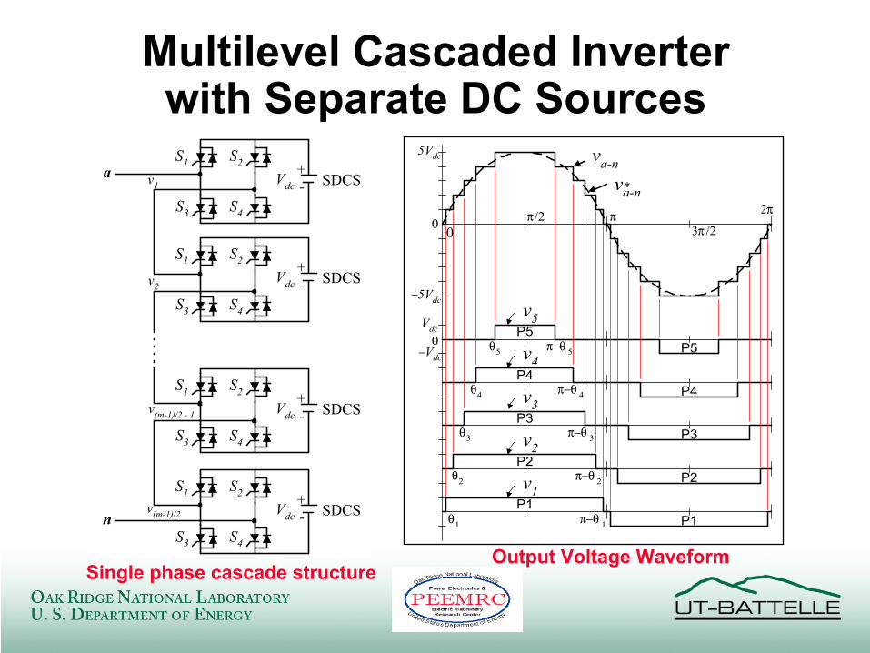
Multilevel Cascaded Inverter with Separate DC Sources
Vs
2
Output Voltage WaveformSingle phase cascade structure
S1
S3
S2
S4
Vdc+- SDCS
S1
S3
S2
S4
Vdc+- SDCS
S1
S3
S2
S4
Vdc+- SDCS
S1
S3
S2
S4
Vdc+- SDCS
a v1
v2
n
v(m-1)/2 - 1
v(m-1)/2
−5Vdc
0π/2 π
3π /2
2π
va-n
va-n
*
v5
v4
v3
v2
v1
0
0Vdc
−Vdc
5Vdc
P1
P2
P3
P4
P5
P1
P2
P3
P4
P5θ5 π−θ 5
θ4
θ1
θ2
θ3
π−θ 1
π−θ 2
π−θ 3
π−θ 4
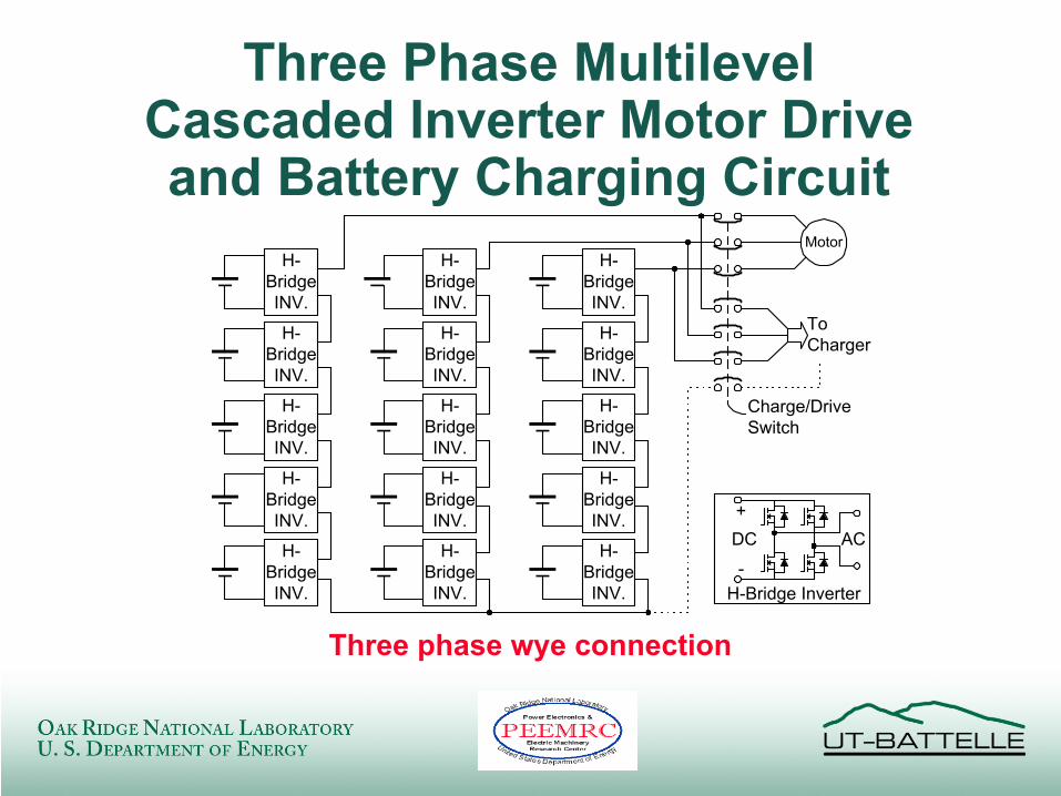
Three Phase Multilevel Cascaded Inverter Motor Drive and Battery Charging Circuit
Three phase wye connection
H-BridgeINV.
H-BridgeINV.
H-BridgeINV.
H-BridgeINV.
H-BridgeINV.
H-BridgeINV.
H-BridgeINV.
H-BridgeINV.
H-BridgeINV.
H-BridgeINV.
H-BridgeINV.
H-BridgeINV.
Motor
ToCharger
Charge/DriveSwitch
DC AC+
-H-Bridge Inverter
H-BridgeINV.
H-BridgeINV.
H-BridgeINV.
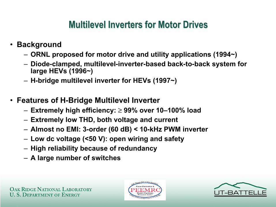
• Background– ORNL proposed for motor drive and utility applications (1994~)– Diode-clamped, multilevel-inverter-based back-to-back system for
large HEVs (1996~)– H-bridge multilevel inverter for HEVs (1997~)
• Features of H-Bridge Multilevel Inverter– Extremely high efficiency: ≥ 99% over 10–100% load– Extremely low THD, both voltage and current– Almost no EMI: 3-order (60 dB) < 10-kHz PWM inverter– Low dc voltage (<50 V): open wiring and safety– High reliability because of redundancy– A large number of switches
Multilevel Inverters for Motor DrivesMultilevel Inverters for Motor Drives
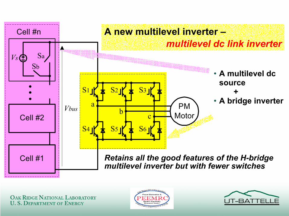
Retains all the good features of the H-bridge multilevel inverter but with fewer switches
Cell #2PM
MotorVbus
Vs Sa
Sb
Cell #1
Cell #n
S1 S2
S6S5S4
S3
ab c
A new multilevel inverter –multilevel dc link inverter
• A multilevel dc source
+• A bridge inverter
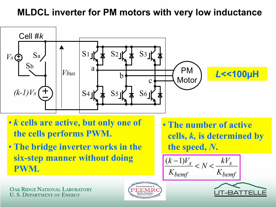
MLDCL inverter for PM motors with very low inductance
PMMotor
Vbus
Vs Sa
Sb
Cell #k
S1 S2
S6S5S4
S3
ab c
(k-1)Vs
• k cells are active, but only one of the cells performs PWM.
• The bridge inverter works in the six-step manner without doing PWM.
bemf
s
bemf
sK
kVNK
Vk <<− )1(
• The number of active cells, k, is determined by the speed, N.
L<<100µH
0
5
10
15
20
25
0 2 4 6 8Speed [krpm]
Iripp
le(p
eak)
[%]
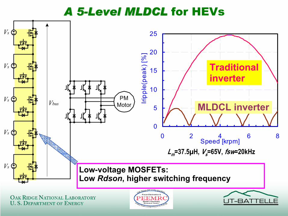
A 5A 5--Level MLDCLLevel MLDCL for HEVs
PMMotorVbus
Vs
Vs
Vs
Vs
Vs
Traditionalinverter
MLDCL inverter
Lm=37.5µH, Vs=65V, fsw=20kHz
Low-voltage MOSFETs:Low Rdson, higher switching frequency
+
-Half-Bridge Cell
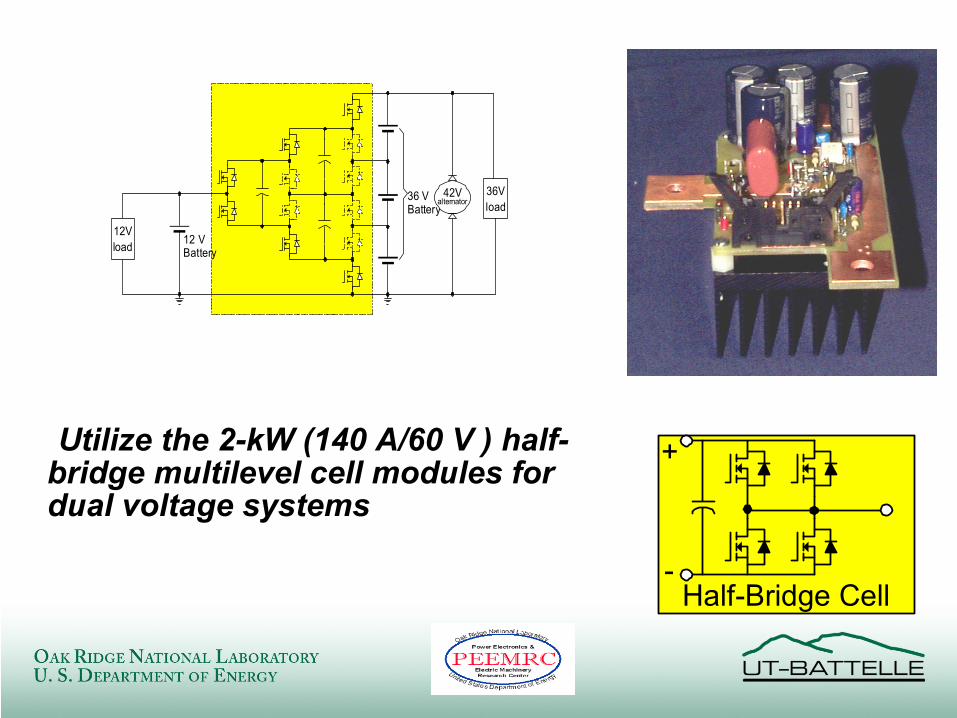
Utilize the 2-kW (140 A/60 V ) half-bridge multilevel cell modules for dual voltage systems
12 VBattery
36 VBattery
12Vload
42Valternator
36Vload

Today’s Technology
Advantages of Silicon Carbide
Payoff
Large energy losses Reduce loss by 10x Large improvement in efficiency
Limited voltage and power level
Increase power 103x Simplify use (no need toseries/parallel devices)
Low operating temperature (<150ºC)
Increase range to 350ºC or higher
New applications; eliminate massive heat sinks
Large heat sinks & filters
Reduce size/weight by 3x
Lightweight, compact systems
Future Power Electronics Will Be SiC
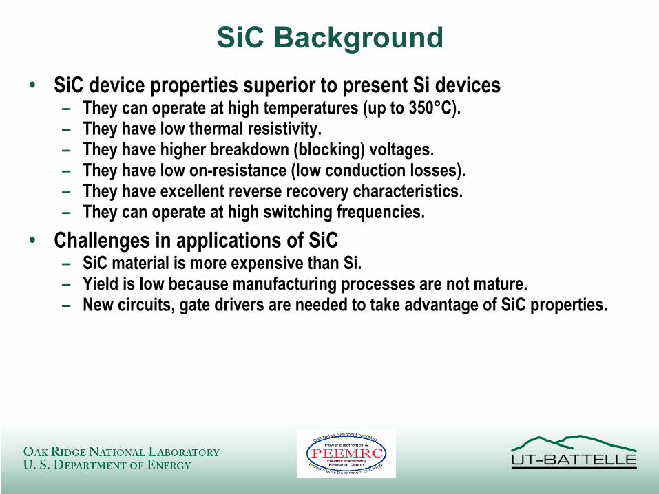
SiC Background• SiC device properties superior to present Si devices
– They can operate at high temperatures (up to 350°C).– They have low thermal resistivity.– They have higher breakdown (blocking) voltages.– They have low on-resistance (low conduction losses).– They have excellent reverse recovery characteristics.– They can operate at high switching frequencies.
• Challenges in applications of SiC– SiC material is more expensive than Si.– Yield is low because manufacturing processes are not mature.– New circuits, gate drivers are needed to take advantage of SiC properties.
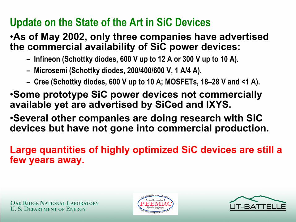
Update on the State of the Art in SiC Devices•As of May 2002, only three companies have advertised the commercial availability of SiC power devices:
– Infineon (Schottky diodes, 600 V up to 12 A or 300 V up to 10 A).– Microsemi (Schottky diodes, 200/400/600 V, 1 A/4 A).– Cree (Schottky diodes, 600 V up to 10 A; MOSFETs, 18–28 V and <1 A).
•Some prototype SiC power devices not commercially available yet are advertised by SiCed and IXYS.•Several other companies are doing research with SiC devices but have not gone into commercial production.
Large quantities of highly optimized SiC devices are still a few years away.
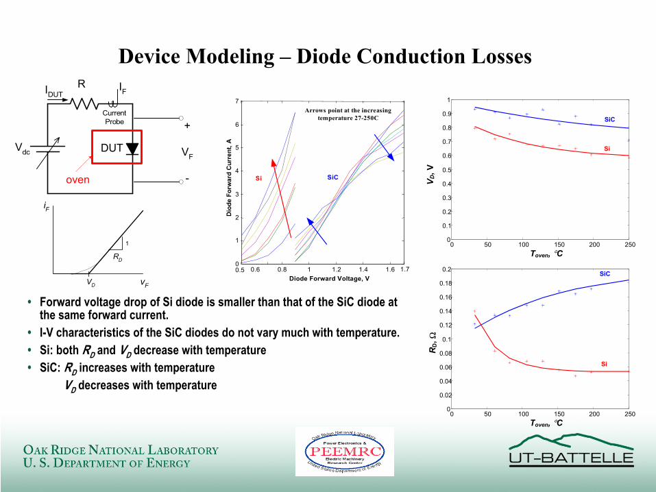
Device Modeling – Diode Conduction Losses
• Forward voltage drop of Si diode is smaller than that of the SiC diode at the same forward current.
• I-V characteristics of the SiC diodes do not vary much with temperature.• Si: both RD and VD decrease with temperature• SiC: RD increases with temperature
VD decreases with temperature
R
DUTVdc
IF
+
VF
-
IDUT
CurrentProbe
oven
0.6 0.8 1 1.2 1.4 1.6 1.70
1
2
3
4
5
6
7
Diode Forward Voltage, V
Dio
de F
orw
ard
Cur
rent
, A
Si SiC
0.5
Arrows point at the increasingtemperature 27-250C
0 50 100 150 200 2500
0.1
0.2
0.3
0.4
0.5
0.6
0.7
0.8
0.9
1
Toven, °C
V D, V
SiC
Si
0 50 100 150 200 2500
0.02
0.04
0.06
0.08
0.1
0.12
0.14
0.16
0.18
0.2
Toven, °CR
D, Ω
SiC
Si
vF
iF
1
RD
VD
0 10 20 30 40 50 60 70 80 90 1000
5
10
15
20
25
30D
iode
Con
duct
ion
Loss
, W
Diode Forward Current, A
SiC
M=.5
Increasing Temperature25, 75, 125, 175, 225°C
0 10 20 30 40 50 60 70 80 90 1000
5
10
15
20
25
30
Dio
de C
ondu
ctio
n Lo
ss, W
Diode Forward Current, A
Si
M=.5Increasing Temperature25, 75, 125, 175, 225°C
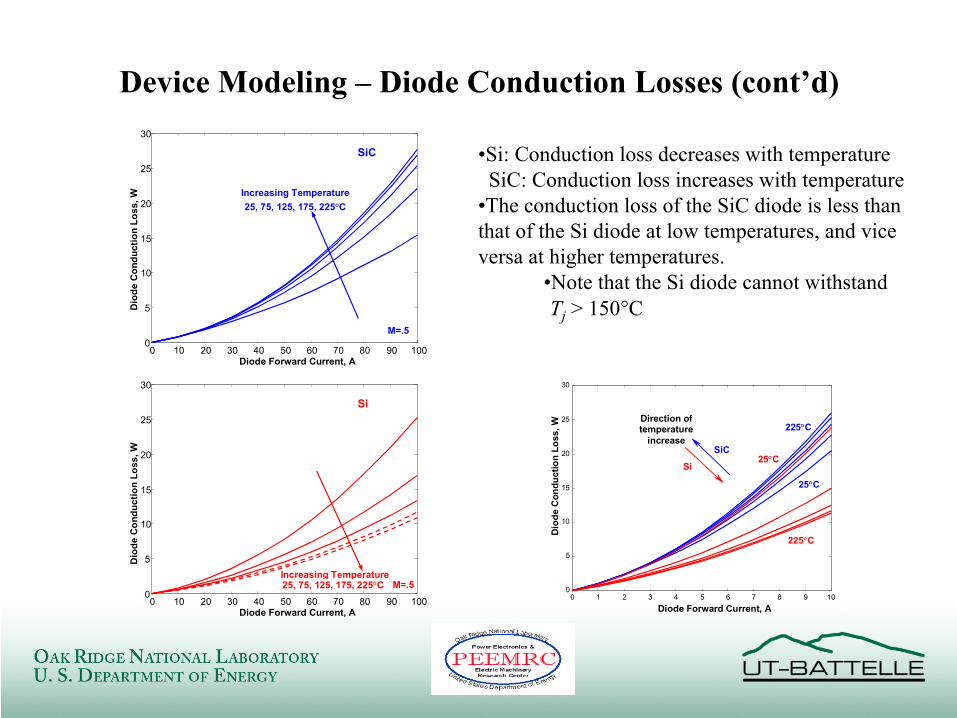
•Si: Conduction loss decreases with temperatureSiC: Conduction loss increases with temperature
•The conduction loss of the SiC diode is less than that of the Si diode at low temperatures, and vice versa at higher temperatures.
•Note that the Si diode cannot withstand Tj > 150°C
0 1 2 3 4 5 6 7 8 9 100
5
10
15
20
25
30
Dio
de C
ondu
ctio
n Lo
ss, W
Diode Forward Current, A
Si
SiC25°C
225°C
25°C
225°CDirection oftemperature
increase
Device Modeling – Diode Conduction Losses (cont’d)
R1
L1
D=DUTVdc
iDUT
CurrentProbe id
+vd-
VoltageIsolator
Q
iL
oven
1 kHz
SiC
Si
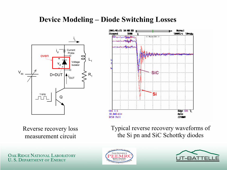
Reverse recovery loss measurement circuit
Typical reverse recovery waveforms of the Si pn and SiC Schottky diodes
Device Modeling – Diode Switching Losses
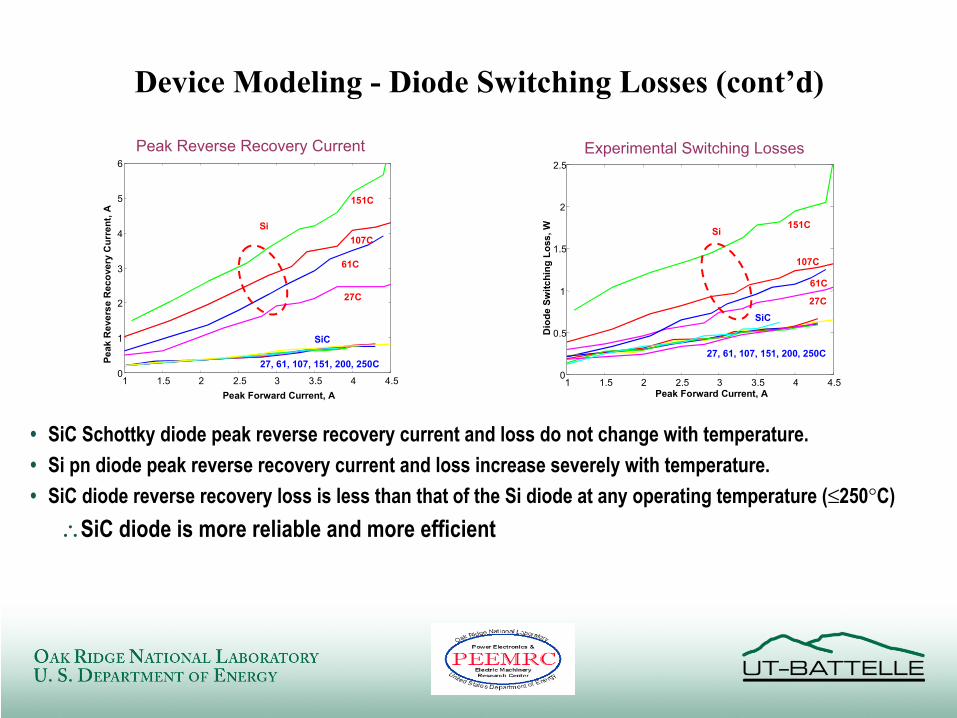
• SiC Schottky diode peak reverse recovery current and loss do not change with temperature.• Si pn diode peak reverse recovery current and loss increase severely with temperature.• SiC diode reverse recovery loss is less than that of the Si diode at any operating temperature (≤250°C)
∴SiC diode is more reliable and more efficient
1 1.5 2 2.5 3 3.5 4 4.50
1
2
3
4
5
6
Peak
Rev
erse
Rec
over
y C
urre
nt, A
Peak Forward Current, A
Si
SiC
27C
61C
107C
151C
27, 61, 107, 151, 200, 250C
1 1.5 2 2.5 3 3.5 4 4.50
0.5
1
1.5
2
2.5
Peak Forward Current, A
Dio
de S
witc
hing
Los
s, W
27, 61, 107, 151, 200, 250C
151C
107C
61C
27C
Si
SiC
Peak Reverse Recovery Current Experimental Switching Losses
Device Modeling - Diode Switching Losses (cont’d)
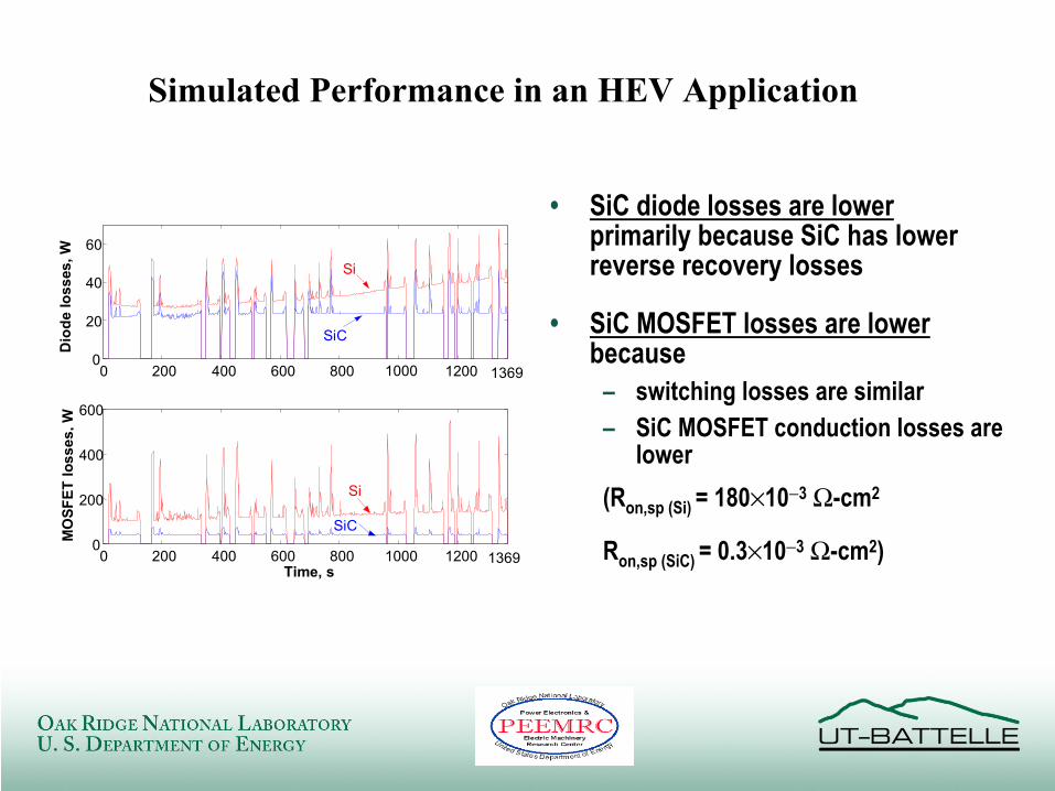
• SiC diode losses are lowerprimarily because SiC has lower reverse recovery losses
• SiC MOSFET losses are lowerbecause
– switching losses are similar– SiC MOSFET conduction losses are
lower (Ron,sp (Si) = 180×10−3 Ω-cm2
Ron,sp (SiC) = 0.3×10⁻³ Ω-cm2)
0 200 400 600 800 1000 12000
20
40
60
Dio
de lo
sses
, W
0 200 400 600 800 1000 12000
200
400
600
Time, s
MO
SFET
loss
es, W
Si
SiC
Si
SiC
1369
1369
Simulated Performance in an HEV Application
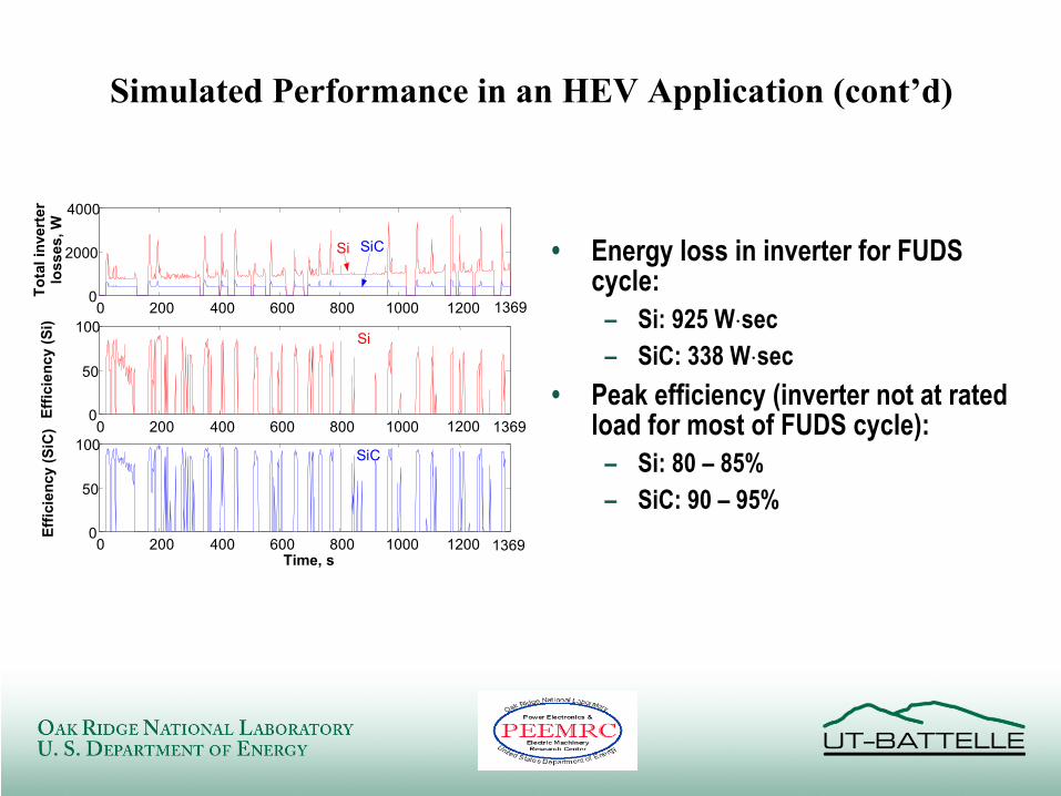
• Energy loss in inverter for FUDS cycle:
– Si: 925 W⋅sec – SiC: 338 W⋅sec
• Peak efficiency (inverter not at rated load for most of FUDS cycle):
– Si: 80 – 85%– SiC: 90 – 95%
0 200 400 600 800 1000 12000
2000
4000
Tota
l inv
erte
rlo
sses
, W
0 200 400 600 800 1000 12000
50
100
Effic
ienc
y (S
i)
0 200 400 600 800 1000 12000
50
100
Effic
ienc
y (S
iC)
Time, s
SiCSi
Si
SiC
1369
1369
1369
Simulated Performance in an HEV Application (cont’d)
• If natural-air-cooled, finned, aluminumheatsinks are used, then
– Si inverter needs a heatsink with a volume of 1998 cm3 and a weight of 5.4 kg
– Si inverter needs a heatsink with a volume of only 606 cm3 and a weight of 1.65 kg
1200450
4200
1200
5400
1650
0
1000
2000
3000
4000
5000
6000
Diodes MOSFETs Inverter
Heatsink Mass (g)
SiSiC
0 200 400 600 800 1000 12000
50
100
150
200
Dio
de J
unct
ion
Tem
pera
ture
, °C
0 200 400 600 800 1000 12000
50
100
150
200
MO
SFET
Jun
ctio
nTe
mpe
ratu
re, °
C
150 C
175 C
150 C
175 C
Si
SiC
Si
SiC
1369
1369Time, s
Simulated Performance in an HEV Application (cont’d)
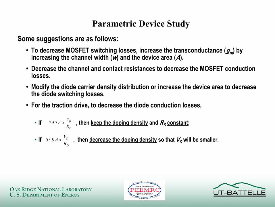
Parametric Device StudySome suggestions are as follows:
• To decrease MOSFET switching losses, increase the transconductance (gm) by increasing the channel width (w) and the device area (A).
• Decrease the channel and contact resistances to decrease the MOSFET conduction losses.
• Modify the diode carrier density distribution or increase the device area to decrease the diode switching losses.
• For the traction drive, to decrease the diode conduction losses,
• If , then keep the doping density and RD constant;
• If , then decrease the doping density so that VD will be smaller.
D
D
RVA >3.29
D
D
RVA <9.55

• Problems and Limitations of existing gate drives– They are operable only at up to 20 kHz switching at high power.– They have a long (1-2µs) propagation delay.– They do not take advantage of SiC’s high-speed and high-temperature operation.
DUT
• Design and build new gate drive– A new gate drive circuit developed for SiC
MOSFETs operated at up to 500 kHz at high temperatures (250°C).
– Test gate drive on SiC MOSFETs developed by ORNL and/or others.
Innovative new circuit designs required to exploit advantages of SiC
New Gate Drives for SiC MOSFETs/IGBTs
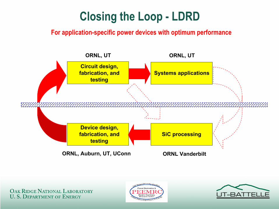
Closing the Loop - LDRD
SiC processingDevice design,fabrication, and
testing
Circuit design,fabrication, and
testingSystems applications
For application-specific power devices with optimum performance
ORNL VanderbiltORNL, Auburn, UT, UConn
ORNL, UT ORNL, UT
• “Effects of Silicon Carbide (SiC) Power Devices on PWM Inverter Losses,” The 27th Annual Conference of the IEEE Industrial Electronics Society (IECON'01), Denver, Colorado, November 29–December 2, 2001, pp. 1187–1192.
• “Impact of SiC Power Electronics for Hybrid Electric Vehicles,” SAE Future Car Congress Proceedings, Arlington, Virginia, June 3 – 5, 2002.
• “Testing, Characterization, and Modeling of SiC Diodes for Transportation Applications,” IEEE Power Electronics Specialists Conference (PESC'02), Cairns, Australia, June 23–27, 2002.
Publications

Related National LaboratoryPower Module Developments
• Fiber Optic Voltage & Current Sensors• DC Buss Capacitors• Snubber Capacitors• Carbon Foam for Thermal Management• Motor Controller Development

Permanent Magnet Motor Field Weakening
• Analyze known field-weakening methods for electronically switched permanent magnet (PM) type motors.
• Identify deficiencies that may limit their use as an HEV drive systems.• Identify ways to mitigate the consequences of these deficiencies.• Compare attributes of all PM motor/drive systems that are FreedomCAR
HEV candidates and recommend one as the PM drive system of choice.

Rotor Assembly(20-kW axial-gap PM motor)
Pre-closure Post-closure Jig removed
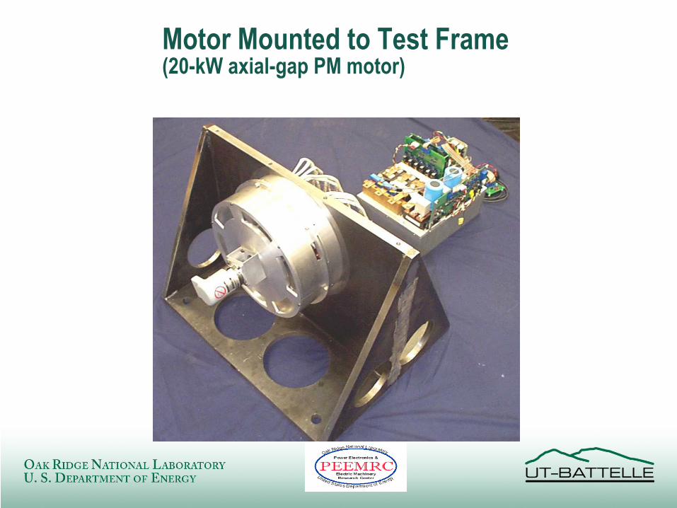
Motor Mounted to Test Frame(20-kW axial-gap PM motor)

DMIC Inverter and Motor in Test Cell 1Ready for Prequalification
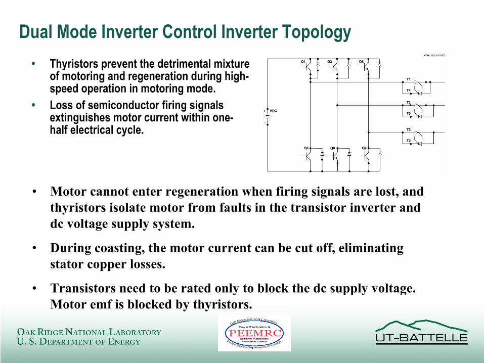
Dual Mode Inverter Control Inverter Topology• Thyristors prevent the detrimental mixture
of motoring and regeneration during high-speed operation in motoring mode.
• Loss of semiconductor firing signals extinguishes motor current within one-half electrical cycle.
• Motor cannot enter regeneration when firing signals are lost, and thyristors isolate motor from faults in the transistor inverter and dc voltage supply system.
• During coasting, the motor current can be cut off, eliminating stator copper losses.
• Transistors need to be rated only to block the dc supply voltage. Motor emf is blocked by thyristors.

Features of the DMIC
• Can drive “low” inductance BDCM over a wide CPSR without exceeding the rated (base speed) rms motor current.
• Can drive “high” inductance BDCM over a wide CPSR without exceeding the rated rms current. Can expect up to 50% more power at high speed.
• Can tolerate large changes in the dc supply voltage. As the dc supply voltage decreases, motor power is reduced, but the rated rms motor current can be maintained.
• Can control both motoring and regenerative braking over the entire speed range.
• Achieves functional equivalent of field weakening without supplementary field windings or exotic rotor/magnet configuration.
Features of the DMIC (continued)
• Each phase “idles” twice during one electrical cycle, allowing position estimation schemes developed for conventional operation below base speed to be extended to operation above base speed. May eliminate the need for an encoder.
• Motor current can be extinguished within half an electrical cycle if the transistor inverter or dc supply system short-circuits.
• Loss of semiconductor firing signals while motoring at high speed results in rapid extinction of motor current rather than deep regenerative braking.
• “Coasting” at high speed does not involve any stator copper losses since the motor current is cut off.
Conclusions• The DMIC can tolerate very large inductance and voltage variations.
– Allows motor designer to optimize design based on machine concerns likely to lead to low inductance.
– Lower inductance decreases dc supply voltage requirements and increases peak power capability.
– Unnecessary to oversize the dc supply, the electric motor, the electronics, and the cooling system when using this technology.
• Coasting losses with the DMIC are solely the hysteresis and eddy current losses of the motor. When CPA is used coasting losses may be an order of magnitude greater.
• The thyristors in the DMIC inverter protect against– shorting the dc bus– loss of the dc bus– loss of firing signals
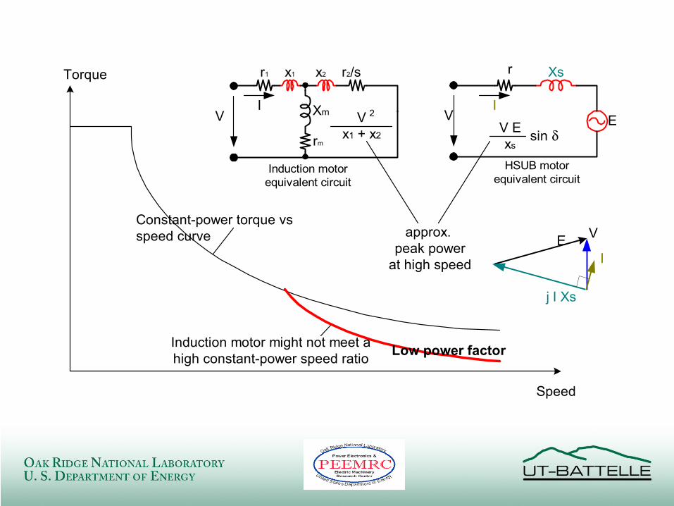
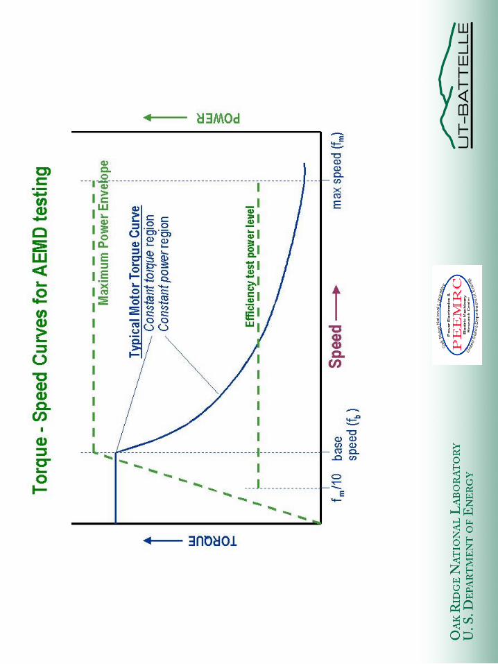
Torque
Speed
VI Xm
r1
VI
Xsr
E
x1 r2/sx2
rm
Induction motorequivalent circuit
HSUB motorequivalent circuit
IE V
j I Xs
Induction motor might not meet ahigh constant-power speed ratio
Constant-power torque vsspeed curve
V Exs
sin δ
approx. peak power
at high speed
Vx1 + x2
2
Low power factor
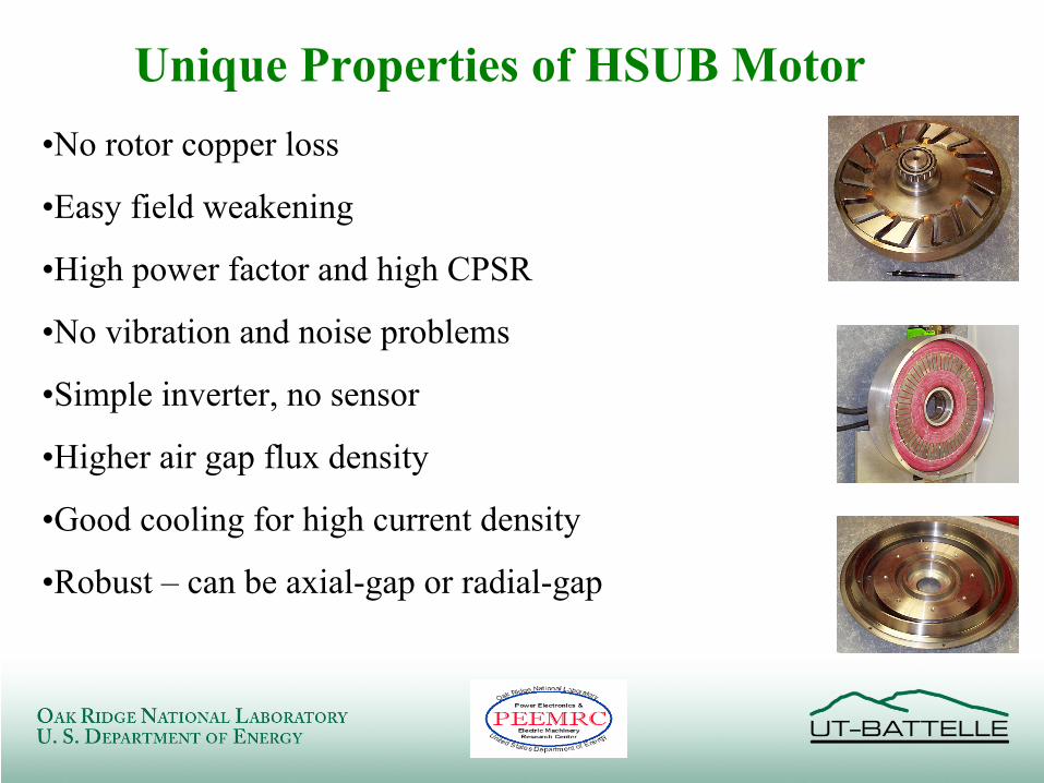
•No rotor copper loss
•Easy field weakening
•High power factor and high CPSR
•No vibration and noise problems
•Simple inverter, no sensor
•Higher air gap flux density
•Good cooling for high current density
•Robust – can be axial-gap or radial-gap
Unique Properties of HSUB Motor
Operation of HSUB Motor•The DC flux produced by an excitation coil is delivered to the rotor through the air gap without any brush.
•The DC flux in the rotor is guided to the north and south poles that interact with the armature.
•The undiffused arrangement provided by PMs guides the flux to the main air gap that faces the armature.
•Both the PMs and the excitation coil can enhance the air-gap flux density. Consequently, a high air-gap torque under a given armature current can be obtained.
•Controlling the current of the excitation coil can weaken the main air-gap flux. A simple power electronics drive required by the HSU-B machine may lower the motor drive system cost.
•Direct cooling of the stationary armature and excitation windings allows high current density.

Locus of current, I, forconstant power
V
IJ I Xs
ELocus of back emf, E,
for constant power
Underexcited
Overexcited
1.0powerfactor
V
I
Xsr(small) E
Equivalent circuit of HSUB motor
High Power Factor from HSUB Motor
• Consumer safety (below 50v)• Low power factor has stronger impact on a 42-
V motor – larger actual silicon area and copper lead size required
• HSUB motor offers high power factor
42-V or 380-V System?
Example: 0.7 PF, 30% area increase
For 380 V: 1 sq.in --> 1.3 sq.in
For 42 V: 9 sq.in -->12.7 sq.in
3.7 sq.in compared with 0.3 sq.in

Laminatedrotor core with
copper bars
Aluminumend ring
Soft Commutated dc Motor
Switched Reluctance Motor Field-Weakened PM Motor
Copper-Aluminum Joining

Project Objectives• Project Goals
The purpose of this project is to develop simulation tools for SiC devices in relevant transportation applications. Once developed, these tools can be used to assess the impact of expected performance gains with SiC devices and determine areas of greatest impact.
• Project Objectives (Tasks) for FY 2002– Updated the state of the art in SiC devices.– Developed models of SiC devices (diodes and MOSFETs).– Simulated performance of an HEV traction drive using these device models.– Performed a parametric analysis to determine device parameters that need to
be modified to improve the system performance of this drive.
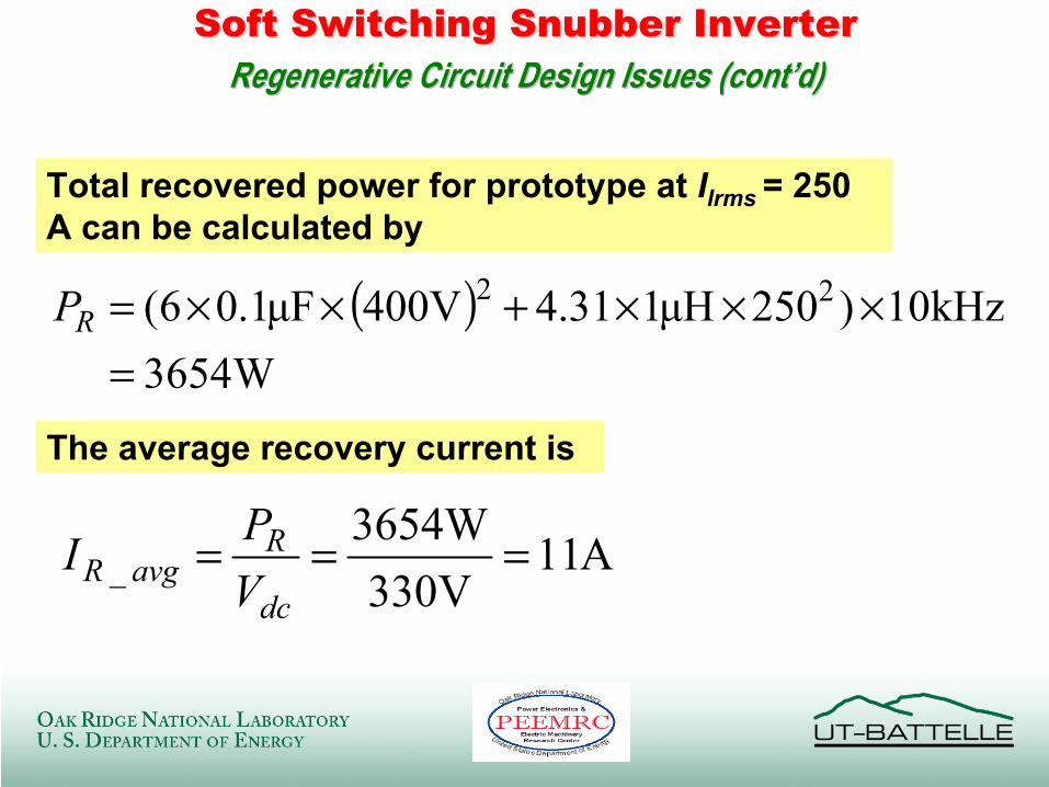
Soft SwitchingSoft Switching SnubberSnubber InverterInverterRegenerative Circuit Design Issues (cont’d)Regenerative Circuit Design Issues (cont’d)
Total recovered power for prototype at Ilrms = 250 A can be calculated by
( )W3654
kHz10)250µH131.4V400µF1.06( 22
=×××+××=RP
The average recovery current is
A11V330
654W3_ ===
dc
RavgR V
PI
Soft SwitchingSoft Switching SnubberSnubber InverterInverterRegenerative Circuit Design Issues (cont’d)Regenerative Circuit Design Issues (cont’d)
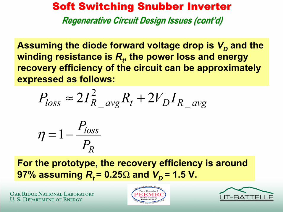
For the prototype, the recovery efficiency is around 97% assuming Rt = 0.25Ω and VD = 1.5 V.
Assuming the diode forward voltage drop is VD and the winding resistance is Rt, the power loss and energy recovery efficiency of the circuit can be approximately expressed as follows:
avgRDtavgRloss IVRIP _2
_ 22 +≈
R
loss
PP−= 1η
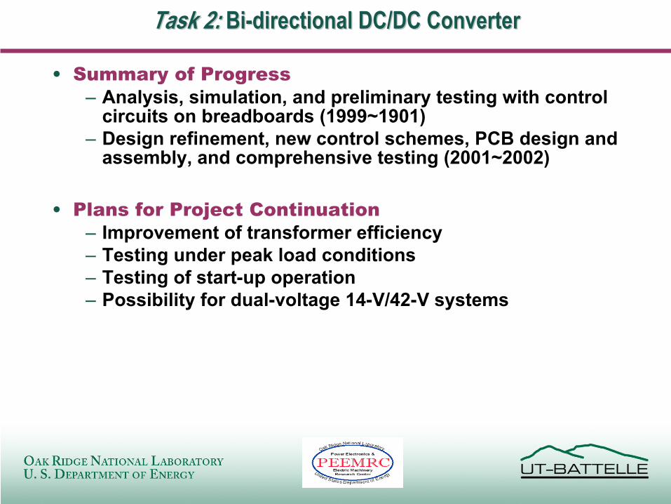
Task 2:Task 2: BiBi--directional DC/DC Converter directional DC/DC Converter
• Summary of Progress– Analysis, simulation, and preliminary testing with control
circuits on breadboards (1999~1901)– Design refinement, new control schemes, PCB design and
assembly, and comprehensive testing (2001~2002)
• Plans for Project Continuation– Improvement of transformer efficiency– Testing under peak load conditions– Testing of start-up operation– Possibility for dual-voltage 14-V/42-V systems
Soft SwitchingSoft Switching SnubberSnubber InverterInverterRegenerative Circuit Design IssuesRegenerative Circuit Design Issues
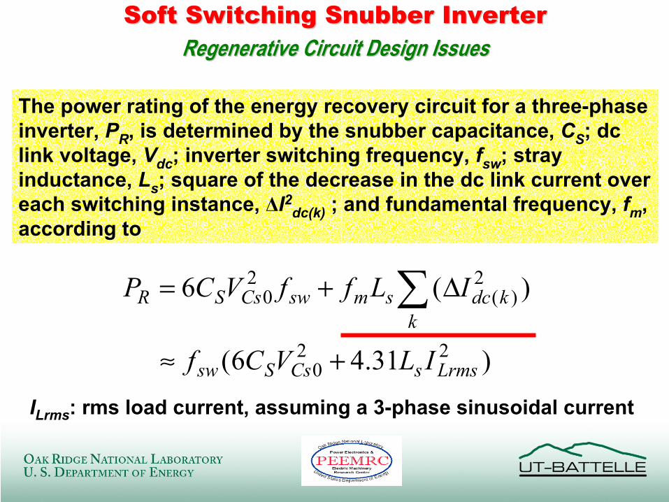
The power rating of the energy recovery circuit for a three-phase inverter, PR, is determined by the snubber capacitance, CS; dc link voltage, Vdc; inverter switching frequency, fsw; stray inductance, Ls; square of the decrease in the dc link current over each switching instance, ∆I2dc(k) ; and fundamental frequency, fm, according to
ILrms: rms load current, assuming a 3-phase sinusoidal current
)31.46(
)(6
220
2)(
20
LrmssCsSsw
kkdcsmswCsSR
ILVCf
ILffVCP
+≈
∆+= ∑
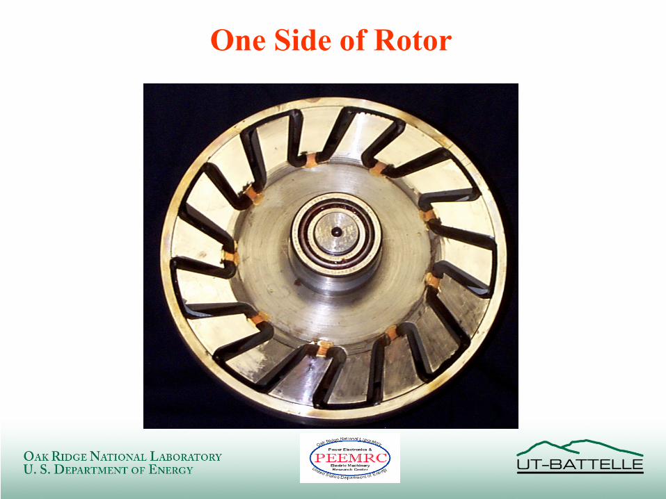
One Side of Rotor
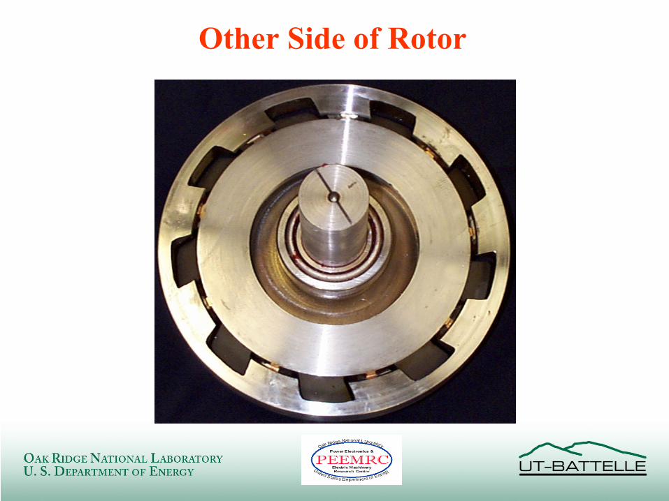
Other Side of Rotor
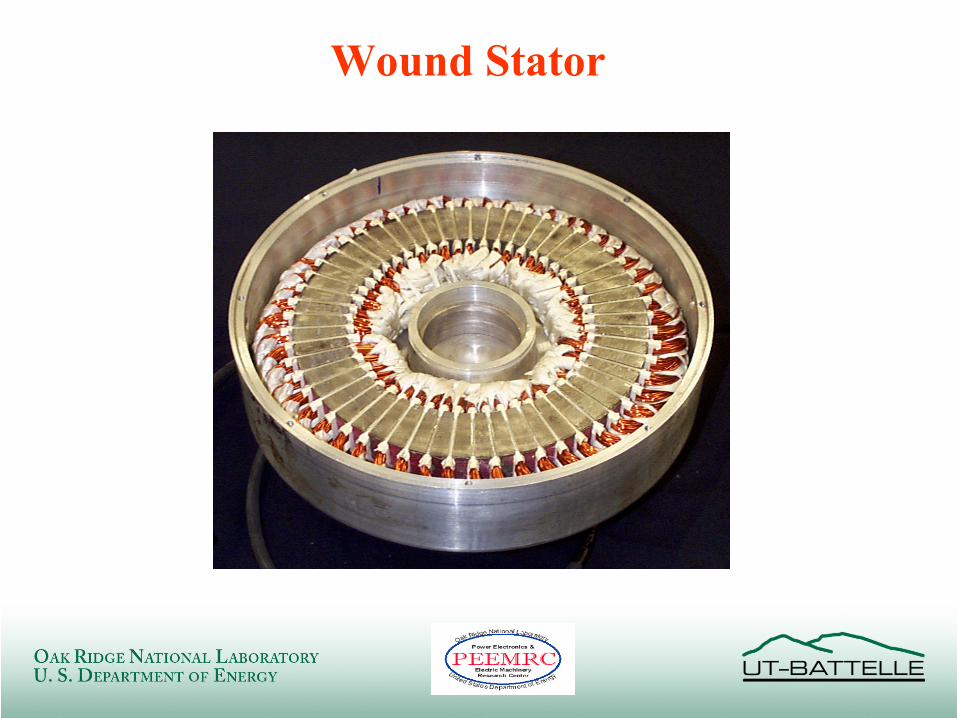
Wound Stator
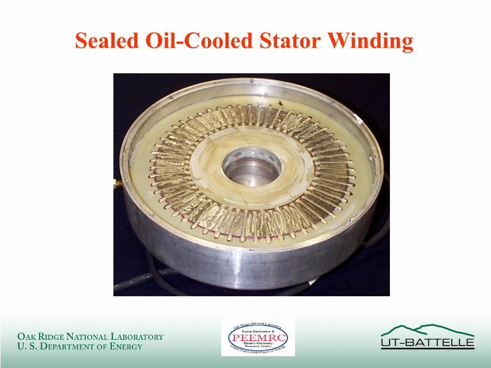
Sealed Oil-Cooled Stator Winding
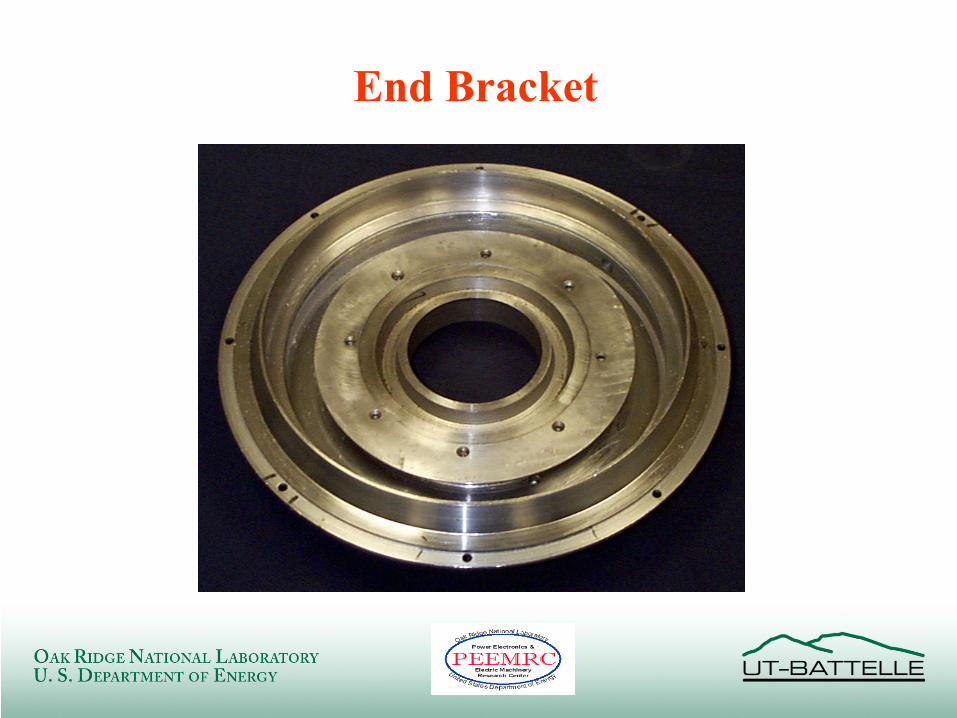
End Bracket
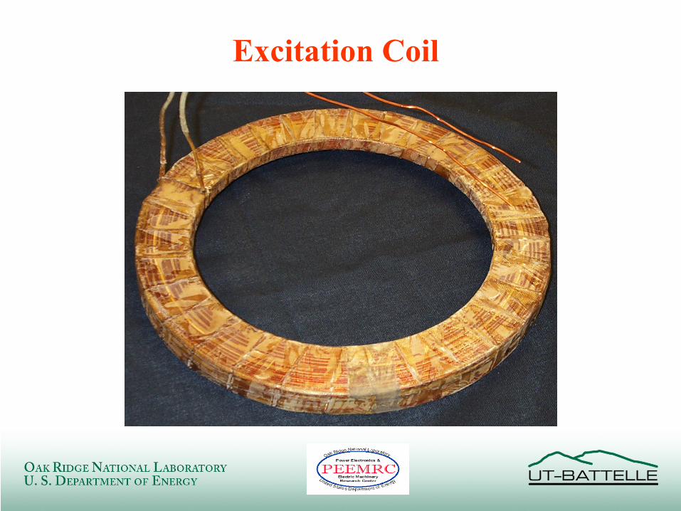
Excitation Coil

End Bracket with Excitation Coil
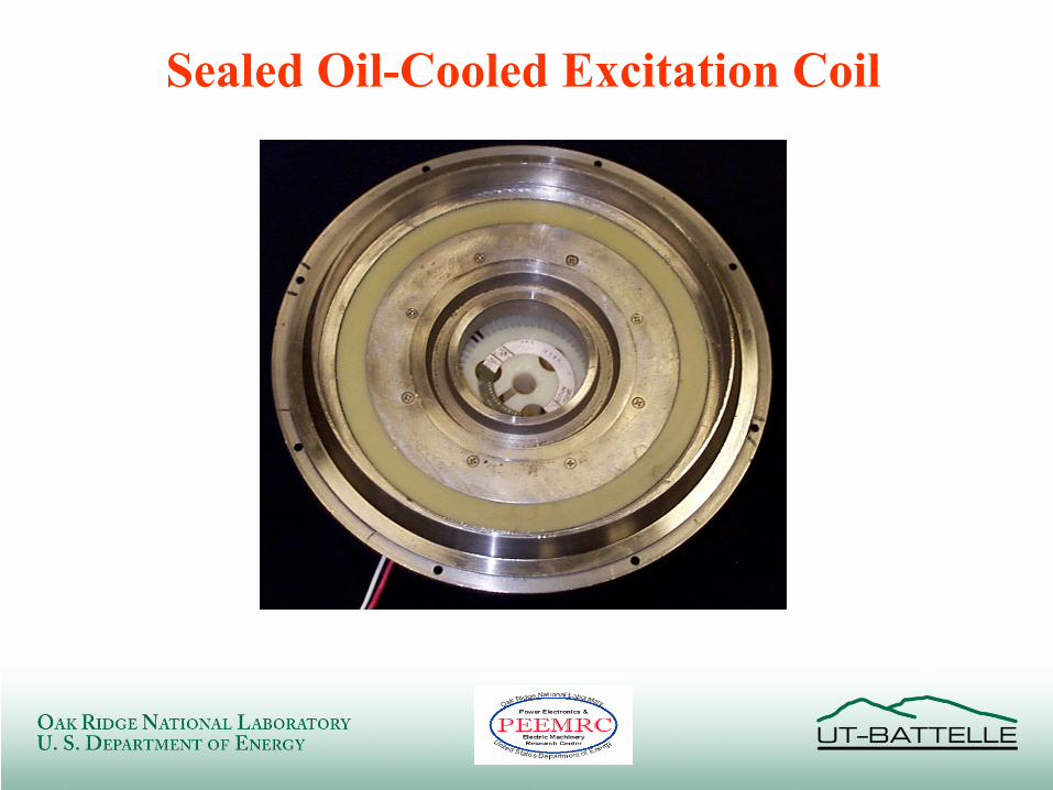
Sealed Oil-Cooled Excitation Coil
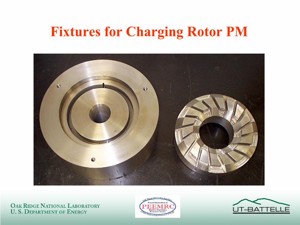
Fixtures for Charging Rotor PM
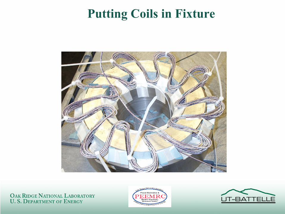
Putting Coils in Fixture

Injected PM Made of MQP-S