Fuel Cell Handbook- Hydrogen Power Electricity Electrical Electronic
JSL1
Future Energy Electronics Center
Power Electronic Technologies for Fuel Cell Power Systems
Dr. Jih-Sheng (Jason) LaiDirector, Future Energy Electronics Center
Virginia Polytechnic Institute and State UniversityBlacksburg, VA 24061-0111
TEL: 540-231-4741FAX: 540-231-3362Email: [email protected]
Presentation atSECA 6th Annual Workshop
Pacific Grove, CaliforniaApril 19, 2005
JSL2
Future Energy Electronics Center
Outline1. Basic Fuel Cell Power Systems2. Non-isolated DC-DC Converters3. Isolated DC-DC Converters4. DC-DC Converter Implementation Issues5. Basic DC-AC Inverters6. Fuel Cell and Converter Interactions 7. Fuel Cell Energy Management Issues8. Advanced V6 DC-DC Converter9. Fuel Cell Current Ripple Issues10. Recap

JSL3
Future Energy Electronics Center
1. Basic Fuel Cell Power Systems
MembraneElectrodeAssembly
(MEA)
MembraneElectrodeAssembly
(MEA)
MembraneElectrodeAssembly
(MEA)
MembraneElectrodeAssembly
(MEA)
1. Fuel Cell ControlFlow ratePressureHumidityTemperature
Fuel in
Core of fuel cell
2. Power ConversionsDC-DC for portableDC-AC for householdDC-variable frequency
AC for automotive
3. Energy storage
Electricityout
Power ElectronicsBOP
JSL4
Future Energy Electronics Center
Automotive Fuel Cell Power System1. Fuel cell control
2. Power conversions
3. Energy storage
JSL5
Future Energy Electronics Center
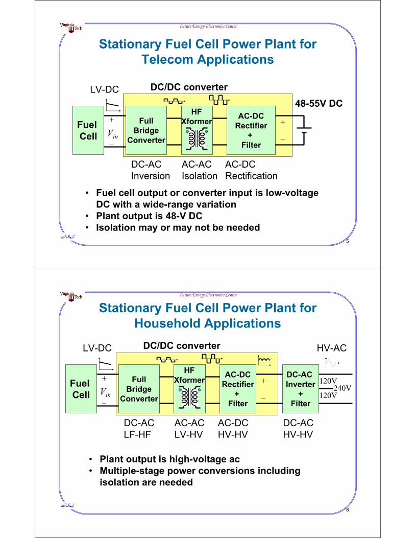
Stationary Fuel Cell Power Plant for Telecom Applications
• Fuel cell output or converter input is low-voltage DC with a wide-range variation
• Plant output is 48-V DC• Isolation may or may not be needed
DC-ACInversion
AC-ACIsolation
AC-DCRectification
FuelCell
AC-DCRectifier
+Filter
Vin
+
–
+
–
FullBridge
Converter
HFXformer
DC/DC converterLV-DC48-55V DC
JSL6
Future Energy Electronics Center
Stationary Fuel Cell Power Plant for Household Applications
• Plant output is high-voltage ac• Multiple-stage power conversions including
isolation are needed
DC-ACLF-HF
AC-ACLV-HV
AC-DCHV-HV
DC-ACHV-HV
DC-ACInverter
+Filter
FuelCell
AC-DCRectifier
+Filter
Vin
+
–
+
–
FullBridge
Converter
HFXformer
DC/DC converterLV-DC HV-AC
120V
120V240V

JSL7
Future Energy Electronics Center
Major Issues Associated with the Power Conditioning Systems
• Cost• Efficiency• Reliability• Isolation• Fuel cell ripple current• Transient response along with auxiliary energy
storage requirement• Communication with fuel cell controller• Electromagnetic interference (EMI) emission
JSL8
Future Energy Electronics Center
2. Basic Non-Isolated DC-DC Converters
• Buck Converter – Output voltage is always lower than input voltage
• Boost Converter – Output voltage is always higher than input voltage
• Buck-boost Converter – Output voltage can be either lower or higher than input voltage

JSL9
Future Energy Electronics Center
Basic Principle of Buck ConverterL
R+Vin
C+Vo
vgs D1
vgs
Vs
Vo
Gate on Gate off
DTs D’Ts
ino DVV
Average output voltage:
g
sd
where D is the duty ratio.Because D < 1, Vo is always less than Vin buckconverting
+Vs(t)
average Vs = Vo
Vs = Vin
Vs = 0
Ts: switching period = 1/fs (s)fs: switching frequency (Hz)
JSL10
Future Energy Electronics Center
A Buck Converter Example
L
+Vin
C+
Vo
vgs
Q1
D1g
sd
+vs(t)48V 24V22 F
40 H
• Input is 48 V, and output is 24 V• Duty cycle D = Vo/Vin = 0.5• Switching frequency = 100 kHz• Output power = 150 W• Inductor and capacitor are designed to limit the current
and voltage ripples
JSL11
Future Energy Electronics Center
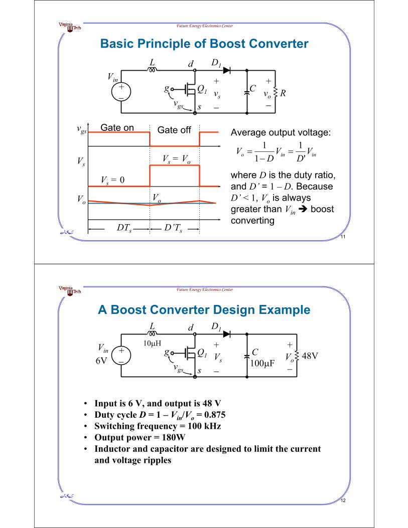
Basic Principle of Boost ConverterL
R+Vin
C+vo
vgs
Q1
D1
vgs
Vs
Vo
Gate on Gate off
DTs D’Ts
g
s
d
Vs = 0
Vs = Voinino V
DV
DV
'1
11
Average output voltage:
where D is the duty ratio, and D’ = 1 – D. BecauseD’ < 1, Vo is always greater than Vin boostconverting
vs
+
Vo
JSL12
Future Energy Electronics Center
A Boost Converter Design ExampleL
+Vin C+Vo
vgs
Q1
D1
g
s
d
Vs
+
6V 48V
• Input is 6 V, and output is 48 V• Duty cycle D = 1 – Vin/Vo = 0.875• Switching frequency = 100 kHz• Output power = 180W• Inductor and capacitor are designed to limit the current
and voltage ripples
10 H
100 F

JSL13
Future Energy Electronics Center
Circuit Diagram of Buck-boost converter
L R+
VinC
+v
vgs
Q1 D1
g
sd
inin VDDV
DDV
'1
+ +
The output voltage can be expressed as
JSL14
Future Energy Electronics Center
Synchronous Rectifier
D
G
S
oxide
S G
n+
D
np+
np+n
i i
• MOSFET can be used as a diode by shorting G-S • However, when running under diode mode, gating
between G-S would allow current to flow through S-D channel in reverse direction synchronous rectification

JSL15
Future Energy Electronics Center
Features of Synchronous Rectification
• MOSFET voltage drop is resistive and can be as low as possible, such as <0.1 V.
• The voltage drop is very crucial to the converter efficiency in a low voltage system. For example, a diode with a fixed voltage drop of 0.7 V represents 3.5% loss of a 20-V system.
• Synchronous rectification allows the voltage drop to be a function of MOSFET resistance and current and cuts the conduction loss substantially. For example, a MOSFET with 5 m running at 20 A condition, the voltage drop is 0.1 V, much less than diode voltage drop.
• Suitable for low-voltage systems.
JSL16
Future Energy Electronics Center
Circuit configuration of a Boost Converter with Synchronous Rectification
• D1 and D2 are body diode of Q1 and Q2.
• Q1 and Q2 switchcomplimentary
Q2
L
R+Vin
C+vo
Q1
D2
D1
vgs1 Q1 on Q1 off
DTs D’Ts
vgs2 Q2 off Q2 on
JSL17
Future Energy Electronics Center
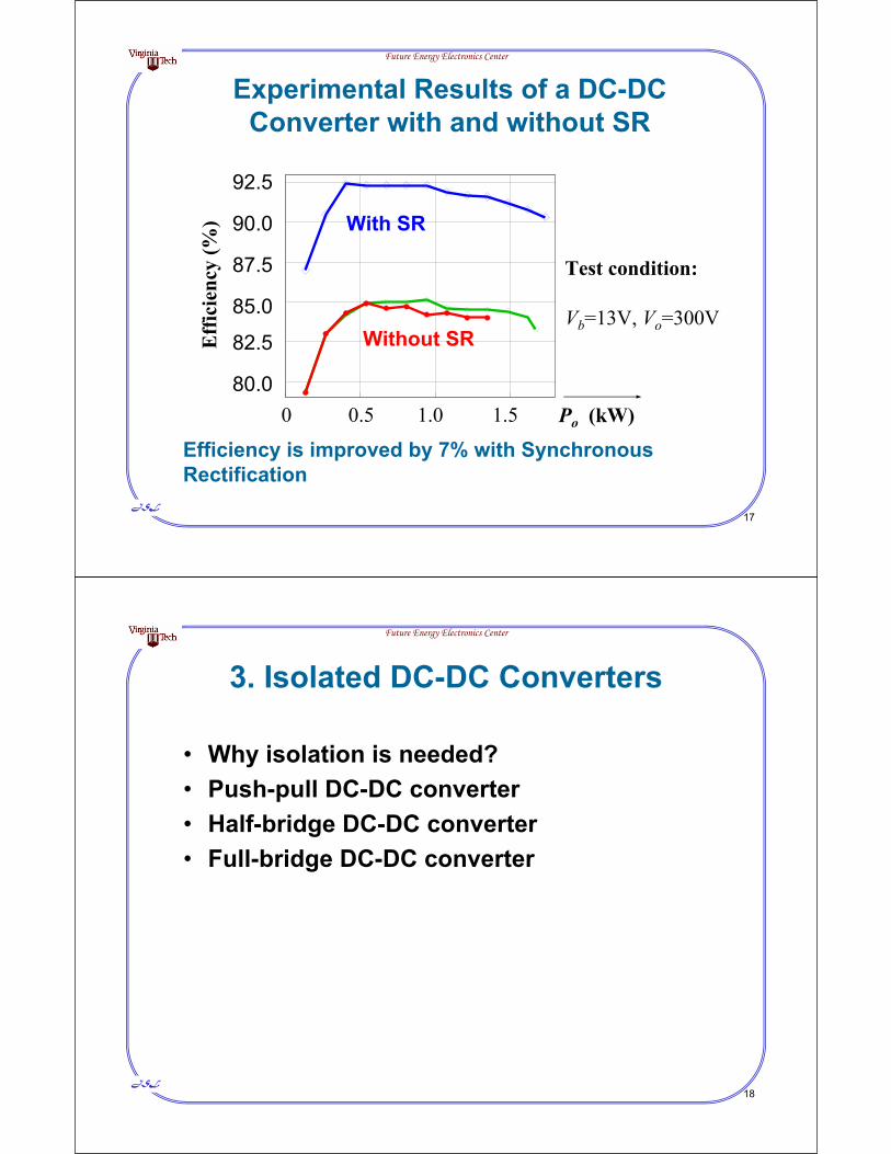
Experimental Results of a DC-DC Converter with and without SR
0 0.5 1.0 1.580.0
82.5
85.0
87.5
90.0
92.5
Po (kW)
With SR
Without SREffi
cien
cy (%
)
Test condition:
Vb=13V, Vo=300V
Efficiency is improved by 7% with Synchronous Rectification
JSL18
Future Energy Electronics Center
3. Isolated DC-DC Converters
• Why isolation is needed?• Push-pull DC-DC converter• Half-bridge DC-DC converter• Full-bridge DC-DC converter

JSL19
Future Energy Electronics Center
Isolation is Required for Most Systems
• High voltage conversion ratios– Isolation allows better device utilization
• Grounding requirement– Isolation avoids noise coupling
• Safety requirement– Isolation allows meeting safety standards
• Multiple outputs– Isolation transformer allows multiple
secondary windings
JSL20
Future Energy Electronics Center
Problems with Isolation
• Magnetic component design and cost are non-trivial
• Transformer saturation due to unbalance input
• Additional losses• Additional terminations

JSL21
Future Energy Electronics Center
Q1
Basic Operating Principle of a Half-Bridge Converter Circuit
VinCf
+
–
Q1
Q2
Half-bridge converter
C1
C2
t
Q1
Q2 Q2vab
dead-time, current circulating thruanti-paralleled diodes
t
t
D2 D1
Vin/20
Switches conduct alternately
vab
2inV
2inV
–+
vab = Vinvab = –Vin
1:n
b
a
JSL22
Future Energy Electronics Center
Half-Bridge DC/DC Converter
Low device countLow voltage deviceDevice sees twice currentUnbalance due to split capacitorsHigh leakage due to twice transformer turns ratio
L
C R vo
+
–
D5
D6
D7
D8
vd
i2
iL
Vin
+
–
1 : nM1
M2
b
C1
a
C2
i1
10V>500A
20V>250A 400V
5 kW

JSL23
Future Energy Electronics Center
Basic Operating Principle of a Push-Pull Converter
1:1:n
Q2 Q1Vin
+
–
C
Q1
t
Q1
Q2 Q2vab
dead-time, current circulating thruanti-paralleled diodes
t
t
D2 D1
2Vin
0
Switches conduct alternatelyvab = 2Vin
vab = –2Vina
b
Push-Pull converter
JSL24
Future Energy Electronics Center
L
C R vo
+
–
D5
D6
D7
D8
vd
i2
iL
Push-Pull DC/DC Converter
+ Simple non-isolated gate drives+ Suitable for low-voltage low-power applications– Device sees twice input voltage – need high voltage MOSFET
High conduction voltage drop, low efficiency– Center-tapped transformer
Difficult to make low-voltage high-current terminations Prone to volt-second unbalance (saturation)
1:1:n
M1 M2Vin
+
–
a
b
40V20V>250A
400V5 kW

JSL25
Future Energy Electronics Center
A Push-Pull Converter with Paralleled Devices
Load
Push-pulldc/dcconverter
DCsource
• Input – 28 to 35 V • Device voltage blocking level – 100 V • Efficiency – <85% even with 4 devices in parallel
JSL26
Future Energy Electronics Center
A Commercial Off-the-Shelf 1-kW Fuel Cell Power Plant Using Push-Pull Converter
Push-pullDC/DC
converter
DCinput
117V
DC/ACInverter
+
–
Fuel
Cel
l

JSL27
Future Energy Electronics Center
Basic Operating Principle of a Full-Bridge Converter Circuit
VinCf
+
–
Q1 Q3
Q2 Q4
a
b
Full-bridge converter
t
Q14 Q14
Q23 Q23vab
dead-time, current circulating thruanti-paralleled diodes
t
t
D23 D14
Vin0
Switches conduct alternately
vab–+
vab = Vinvab = –Vin
1:n
JSL28
Future Energy Electronics Center
Full-Bridge DC/DC Converter
Most popular circuit today for high-power applicationsSoft switching possibleReasonable device voltage ratings
High component count from the look High conduction losses
L
C R vo
+
–
D5
D6
D7
D8
vd
i2
iL
Vin
+
–
1 : nM1 M3
M2 M4
a
b
i1
20V>250A
20V>250A
400V5 kW
JSL29
Future Energy Electronics Center
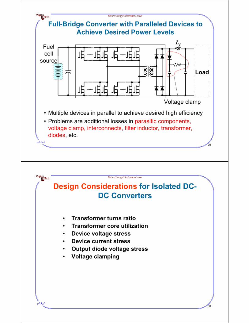
Full-Bridge Converter with Paralleled Devices to Achieve Desired Power Levels
Load
Fuelcell
source
• Multiple devices in parallel to achieve desired high efficiency • Problems are additional losses in parasitic components,
voltage clamp, interconnects, filter inductor, transformer, diodes, etc.
Lf
Voltage clamp
JSL30
Future Energy Electronics Center
Design Considerations for Isolated DC-DC Converters
• Transformer turns ratio• Transformer core utilization• Device voltage stress• Device current stress• Output diode voltage stress• Voltage clamping

JSL31
Future Energy Electronics Center
Pulse Width Modulation for Isolated DC-DC Converters
The average output voltage Vo = DnVin
Wheren = transformer turns ratio = n2/n1D = duty ratio = ton/T
andn1 = number of turns of primary windingn2 = number of turns of secondary winding
ton = switch turn-on timeT = switching period
JSL32
Future Energy Electronics Center
Transformer Core Utilization
Forward: <50% Flyback: <50%
iM
Half-bridge: 100%Push-pull: 100% Full-bridge: 100%
iM-pk
B
HNiM-pk
B
H
iMMagnetizing current
0 0
iM-pk
t t
Core is fully utilized
–NiM-pk
NiM-pk
Core is half utilized
JSL33
Future Energy Electronics Center
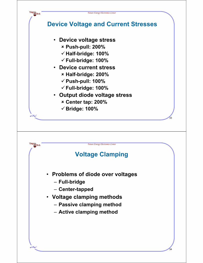
Device Voltage and Current Stresses
• Device voltage stressPush-pull: 200%Half-bridge: 100%Full-bridge: 100%
• Device current stressHalf-bridge: 200%Push-pull: 100%Full-bridge: 100%
• Output diode voltage stressCenter tap: 200%Bridge: 100%
JSL34
Future Energy Electronics Center
Voltage Clamping
• Problems of diode over voltages– Full-bridge– Center-tapped
• Voltage clamping methods – Passive clamping method– Active clamping method
JSL35
Future Energy Electronics Center
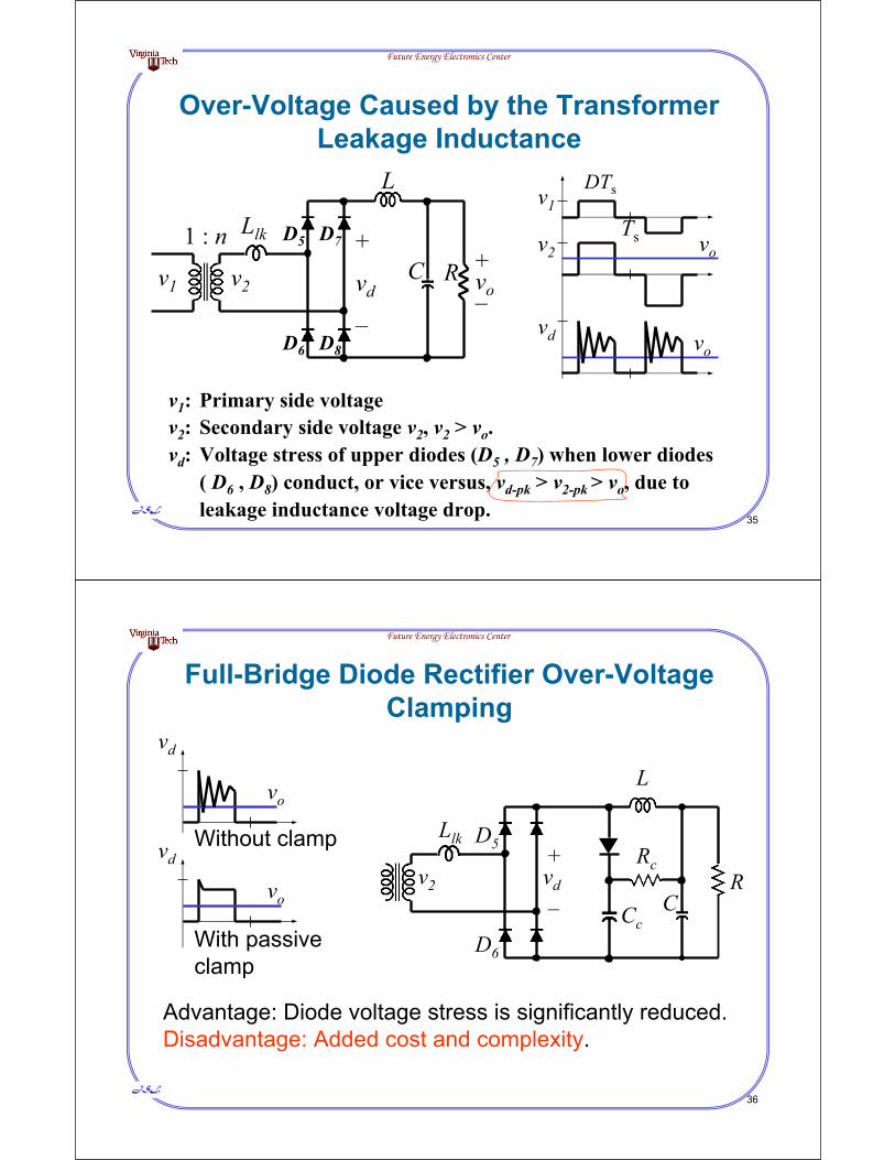
Over-Voltage Caused by the Transformer Leakage Inductance
L
C R vo+
–
1 : n Llk
DTs
v1 v2 vd
–
+
vo
v1
v2
vd
vo
v1: Primary side voltagev2: Secondary side voltage v2, v2 > vo.vd: Voltage stress of upper diodes (D5 , D7) when lower diodes
( D6 , D8) conduct, or vice versus, vd-pk > v2-pk > vo, due to leakage inductance voltage drop.
TsD5
D6
D7
D8
JSL36
Future Energy Electronics Center
Full-Bridge Diode Rectifier Over-Voltage Clamping
L
CR
Llk
v2
D5
D6
Cc
Rc
vo
vd
vo
vdWithout clamp
With passive clamp
vd
–
+
Advantage: Diode voltage stress is significantly reduced.Disadvantage: Added cost and complexity.

JSL37
Future Energy Electronics Center
Fuel Cell System Example for Topology Selection
Question: With 48 V fuel cell voltage and 400 V dc output, what topology is the best?
Answer: Intuitively, push-pull converter is the best because of least parts count. However, with device availability and cost consideration, full-bridge convertermay be a better choice.
Reason: For low-side power MOSFET, lower voltage is more cost effective. Similarly, for high-side diode, lower voltage is more cost effective.
JSL38
Future Energy Electronics Center
4. Implementation Issues in High Power DC/DC Converters
• Controller output duty cycles tend to be unbalanced due to internal chip layout, resulting transformer saturation.
• Voltage sensing problem:– Feedback voltage signal tends to be corrupted by noises– Hall sensor is expensive– Common mode and isolation are difficult to deal with
resistor dividers • Current sensing problems:
– Lossy with resistor sensing– Difficult to insert Hall sensor for device current
measurement

JSL39
Future Energy Electronics Center
Full-bridge Converter Design Example
• Specifications:– Input fuel cell voltage ranges from 36 V to 60 V – Output: 400 V, 10 kW
• Current– Output: 25 A – Input: 208 A
JSL40
Future Energy Electronics Center
Power Stage Design
Vin
L
Cf
+
–
C R vo
+
–
1 : nQ1 Q3
Q2 Q4
a
b
HF ac
Xformer
Component Design and Selection: • Power MOSFET• Rectifier diode • Transformer • Filter inductor• Filter capacitor
D5
D6
D7
D8
vd
i1 i2
iL
JSL41
Future Energy Electronics Center
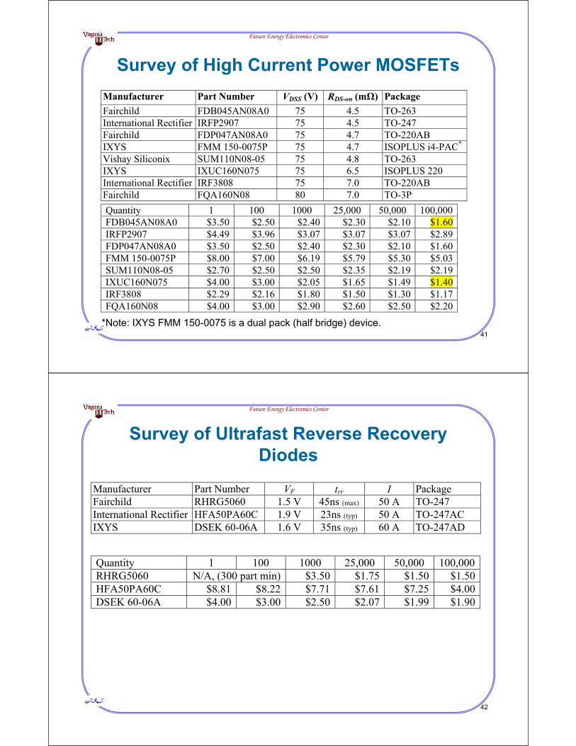
Survey of High Current Power MOSFETs
*Note: IXYS FMM 150-0075 is a dual pack (half bridge) device.
Manufacturer Part Number VDSS (V) RDS-on (m ) Package Fairchild FDB045AN08A0 75 4.5 TO-263 International Rectifier IRFP2907 75 4.5 TO-247 Fairchild FDP047AN08A0 75 4.7 TO-220AB IXYS FMM 150-0075P 75 4.7 ISOPLUS i4-PAC*
Vishay Siliconix SUM110N08-05 75 4.8 TO-263 IXYS IXUC160N075 75 6.5 ISOPLUS 220 International Rectifier IRF3808 75 7.0 TO-220AB Fairchild FQA160N08 80 7.0 TO-3P Quantity 1 100 1000 25,000 50,000 100,000FDB045AN08A0 $3.50 $2.50 $2.40 $2.30 $2.10 $1.60IRFP2907 $4.49 $3.96 $3.07 $3.07 $3.07 $2.89FDP047AN08A0 $3.50 $2.50 $2.40 $2.30 $2.10 $1.60FMM 150-0075P $8.00 $7.00 $6.19 $5.79 $5.30 $5.03SUM110N08-05 $2.70 $2.50 $2.50 $2.35 $2.19 $2.19IXUC160N075 $4.00 $3.00 $2.05 $1.65 $1.49 $1.40IRF3808 $2.29 $2.16 $1.80 $1.50 $1.30 $1.17FQA160N08 $4.00 $3.00 $2.90 $2.60 $2.50 $2.20
JSL42
Future Energy Electronics Center
Survey of Ultrafast Reverse Recovery Diodes
Quantity 1 100 1000 25,000 50,000 100,000RHRG5060 N/A, (300 part min) $3.50 $1.75 $1.50 $1.50HFA50PA60C $8.81 $8.22 $7.71 $7.61 $7.25 $4.00DSEK 60-06A $4.00 $3.00 $2.50 $2.07 $1.99 $1.90
Manufacturer Part Number VF trr I PackageFairchild RHRG5060 1.5 V 45ns (max) 50 A TO-247International Rectifier HFA50PA60C 1.9 V 23ns (typ) 50 A TO-247AC IXYS DSEK 60-06A 1.6 V 35ns (typ) 60 A TO-247AD

JSL43
Future Energy Electronics Center
Output Filter Capacitor Selection- Typically based on the output voltage ripple
• The output filter capacitor needs to handle 120 Hz, 22 A ripple current generated from the next stage inverter.
• Assume the voltage ripple is limited to 5%. The capacitance can be calculated as
mF2.205.0400608
228 Vf
IC
JSL44
Future Energy Electronics Center
Digital Computer Implementation for High Power DC/DC Converters
• Digital computer such as DSP has become a good option for high power DC/DC converter control implementation
• Feedback voltage signal can be converted to digital and through PWM feeding back to DSP to avoid noise corruption
• Even if commercial PWM or PSM chips are used, the control signal can be obtained from DSP through D/A conversion
• Communication with digital signals has become the essential part between the dc/dc converter and the fuel cell controller or other power converters

JSL45
Future Energy Electronics Center
Controller Design for a Typical Converter
21)(
sQsKsGp
sKKsG i
pc )(
Compensator Converter(plant)
Sensor
Reference Output
(A standard PI controller)
Gc(s)Gp(s)
s = j = 2 f
1j
f = frequency
JSL46
Future Energy Electronics Center
Digital Controller for a Typical Converter
DigitalControllerA/D
(sample)D/A
(hold)
Converter
plant
Sensor
ReferenceOutput
11
2)(
zzTKKzG s
ipc
+
–
Ts = switching frequency
112
zz
Ts
s
Gc(s)
JSL47
Future Energy Electronics Center
Voltage Loop Controller Block Diagram
Full BridgeConverter
Vin
L+
–
C R vo
+
–vd
iL
H
Gc(s) –
+
vref
Pulse-widthmodulator
d(t)vsensevc
H: Voltage scaling = 5.1/400 Gc(s): PI or PID Controller
Gp(s)
JSL48
Future Energy Electronics Center
Phase Margin Shifts due to Fuel Cell Input Voltage Variation: 42 to 60 V
0dB from initial designG
ain
(dB
)P
hase
(°)
22 /)/(1)(
oo
invd sQs
nVsG
a negative phase margin with higher gain or higher input voltage
0dB with higher gain or input voltage

JSL49
Future Energy Electronics Center
DC-DC Converter Control System Design is Challenging with the Fuel Cell Source
• A typical controller is designed with low input voltageand heavy load condition.
• When the load is reduced, the fuel cell voltage increases, and the original controller design may be inadequate due to input voltage variation.
• Increasing the input voltage is equivalent to increase the closed-loop gain and tends to worsen the phase margin, and the system can eventually become unstable.
JSL50
Future Energy Electronics Center
5. DC/AC Inverters
• Single-phase output – Half-bridge– Full-bridge
• Dual single-phase outputs – Dual half-bridge– Three-leg inverter
• Load Effect – Linear loads– Nonlinear loads

JSL51
Future Energy Electronics Center
Half-Bridge DC-AC Inverter with Split DC Buses
Q1
Q2
Vdc
L+
–
C ACLoad
Vdc1
Vdc2
vacvab
Maximum output peak voltage Vmax = Vdc/2• Simple dc-ac Inverter with minimum switch counts• Split dc buses should be very stiff and balance to avoid dc or
even harmonics at the ac output• Control is limited to the ordinary sinusoidal pulse width
modulation (SPWM)• Cost burden is in passive components
b
a
Vdc1 = Vdc2 = Vdc/2
c
vba vac
JSL52
Future Energy Electronics Center
Sinusoidal Pulse Width Modulation
vsin
vc : carrier wave
Gating signal
When vsin > vc, gate signal is high, and IGBT is turned on;Otherwise, gate signal is low and IGBT is turned off.
JSL53
Future Energy Electronics Center
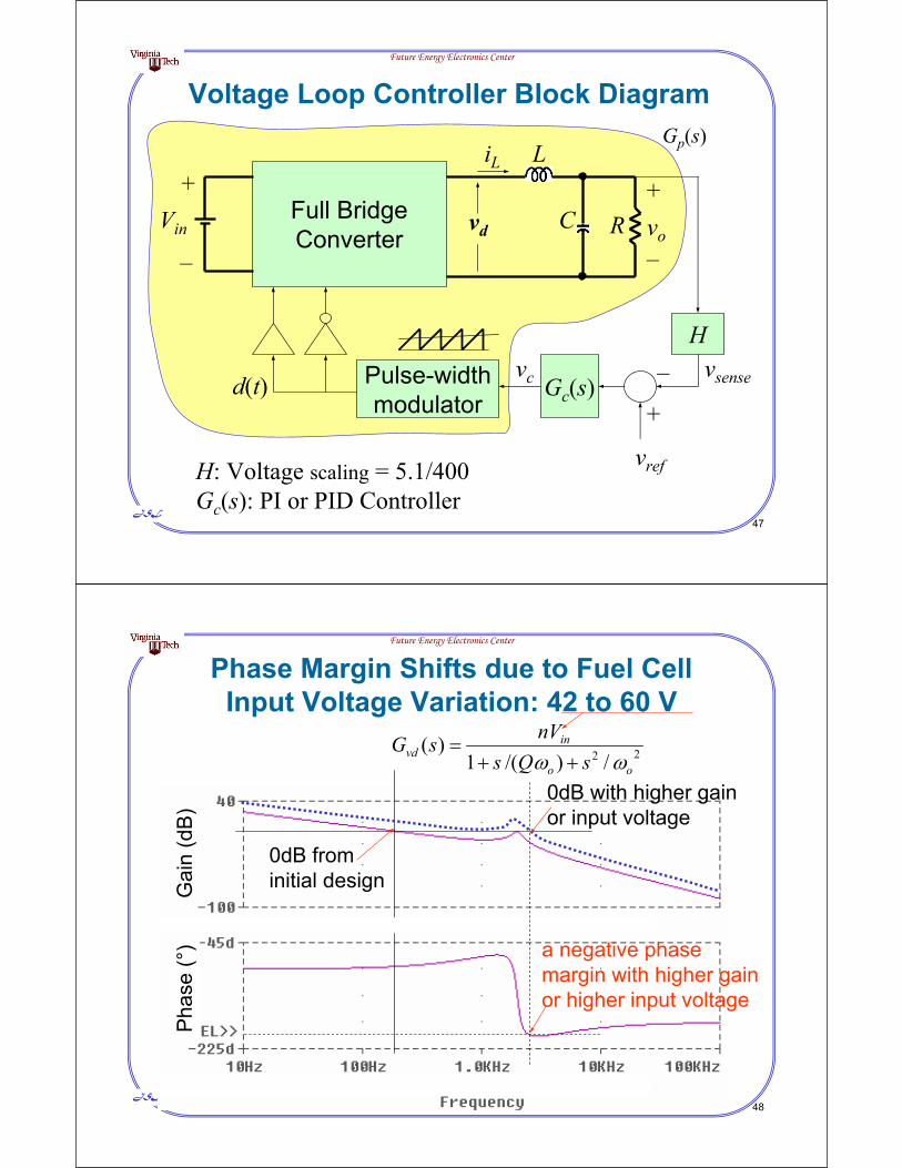
Single-Phase Full-Bridge DC-AC Inverter
Q1 Q3
Q2 Q4
Vdc
LCdc
+
–
C AC Load
Compared with Half-Bridge inverter, FB inverter features• Simple dc-ac Inverter with more switch counts, but
less bulky capacitors• Control is more flexible to have phase-shifted SPWM
for two individual legs – Dual Modulation Method. • Size of passive components may be reduced
JSL54
Future Energy Electronics Center
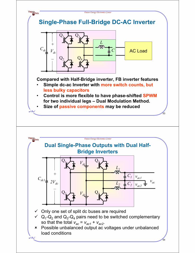
Dual Single-Phase Outputs with Dual Half-Bridge Inverters
Q1
Q2
2VdcCdc1
+
–
Vdc
Vdc
vac1
Q3
Q4
L1
C1
L2 C2 vac2
Only one set of split dc buses are requiredQ1-Q2 and Q3-Q4 pairs need to be switched complementary so that the total vac = vac1 + vac2.Possible unbalanced output ac voltages under unbalanced load conditions
vac

JSL55
Future Energy Electronics Center
Three-leg Inverter for Dual AC Outputs with Single DC Bus
Q1
Q2
VdcCdc
+
–
vac1
Q5
Q6
L1
C1
L3 C2 vac2
vac
Q3
Q4
• Similar to full-bridge inverter with more switch counts, but less bulky capacitors
• Outer legs do SPWM to produce vac output. Middle leg is controlled to equalize vac1 and vac2
• Control is more complicated to ensure output voltage balance• Size of passive components may be reduced
L2
JSL56
Future Energy Electronics Center
Using Low-Frequency Transformer for Low-Voltage AC Inverter Output
L
C48V
120V
120V
240V
Features:• Low-frequency transformer allows low-voltage DC to be
directly converted to AC• Output can be single or dual• Size is the major concern

JSL57
Future Energy Electronics Center
Inverter Output with Resistive Load
RVI
V = 4.1%
vac
Voltage and current are in phase
RvI ac
R
IR
R
JSL58
Future Energy Electronics Center
Dual Output Voltage and Current with Unbalanced and Reactive Loads
Voltage of Leg 1
Current of Leg 1
Voltage of Leg 2
Current of Leg 2
JSL59
Future Energy Electronics Center
-1.0
-0.50.0
0.5
1.0
0 90 180 270 360 450 540 630 720
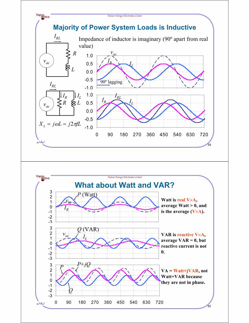
Majority of Power System Loads is Inductive
fLjLjX L 2
vac
IRL
R
L
Impedance of inductor is imaginary (90º apart from real value)
-1.0
-0.5
0.0
0.5
1.0
0 90 180 270 360 450 540 630 720
vac
IRR L
IL IRL
IR
IL
IRL
vac
IL
IR
90º lagging
JSL60
Future Energy Electronics Center
-3-2-10123
0 90 180 270 360 450 540 630 720
-3-2-10123
0 90 180 270 360 450 540 630 720
-3-2-10123
0 90 180 270 360 450 540 630 720
What about Watt and VAR?
P
Q
P+jQ
ILvac
Q (VAR)
IR
vac
P (Watt)
VAR is reactive V A,average VAR = 0, but reactive current is not 0.
Watt is real V A,average Watt > 0, and is the average (V A).
VA = Watt+jVAR, not Watt+VAR because they are not in phase.

JSL61
Future Energy Electronics Center
Implications of VAR
• Average VAR = 0 No real power output• VAR loads are typically inductive such as
motors, magnetic ballasts, relays, etc. • The current associated with VAR causes
additional heat losses in the wiring and the internal impedance of the source
• Inductive VAR can be compensated with capacitive VAR, but not without complexity
• Nonlinear loads also introduce VAR
JSL62
Future Energy Electronics Center
Majority of Electronic Loads is Nonlinear
SwitchModePowerSupply
DCLoad
1-phaserectifier
InverterDrive
ACMotor
3-phaserectifier
Used for:Computers,Printers, Fax, most ITEElectronic LightingCommunicationsFood Preparation
Used for:HVAC, Battery Charging, Food Preparation,Elevators
JSL63
Future Energy Electronics Center
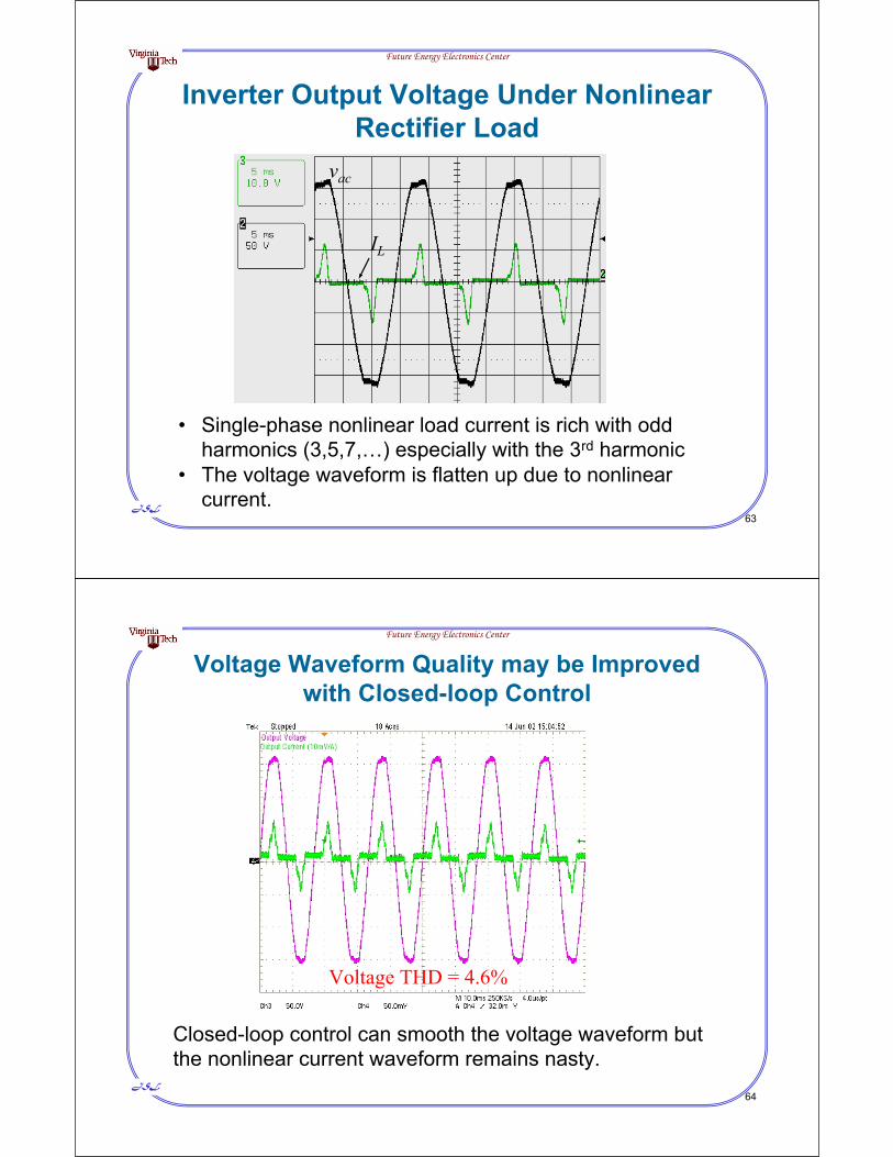
Inverter Output Voltage Under Nonlinear Rectifier Load
• Single-phase nonlinear load current is rich with odd harmonics (3,5,7,…) especially with the 3rd harmonic
• The voltage waveform is flatten up due to nonlinear current.
IL
vac
JSL64
Future Energy Electronics Center
Voltage Waveform Quality may be Improved with Closed-loop Control
Voltage THD = 4.6%
Closed-loop control can smooth the voltage waveform but the nonlinear current waveform remains nasty.

JSL65
Future Energy Electronics Center
6. Fuel Cell and Converter Interactions
• Static modeling• Dynamic modeling• Fuel cell dynamic response with and without
converters
JSL66
Future Energy Electronics Center
SOFC Voltage-Current Characteristic as a Function of Temperature
0.4
0.5
0.6
0.7
0.8
0.9
1
1.1
0 0.2 0.4 0.6 0.8 1 1.2 1.4 1.6 1.8
800 ºC
Current (A/cm2)
Vol
tage
(V)
750 ºC
700 ºC
Data source: DOE SECA Modeling team report at Pittsburgh Airport, 10/15/2002
PEMFC
SOFC

JSL67
Future Energy Electronics Center
Power Density of SOFC and PEMFC
0.0
0.2
0.4
0.6
0.8
1.0
0 0.2 0.4 0.6 0.8 1 1.2
800 ºC
Current (A/cm2)
Pow
er d
ensi
ty (W
/cm
2 )
750 ºC
PEMFC
SOFC
JSL68
Future Energy Electronics Center
PEM Fuel Cell Dynamic Characteristics
0102030405060
0 2 4 6 8 10 12t (sec)
0
500
1000
1500
2000
0 2 4 6 8 10 12t (sec)
vFC(V)
iFC(A)
pFC(W)Step load: 1.47kWParasitic power: 70W
voltage undershoot (2.5V)due to compressor delay
150W dip
27.2V
3kW power overshoot
43V
Nexa 1.2kW Unit

JSL69
Future Energy Electronics Center
Fuel Cell Modeling with Electrical Circuit
load
JSL70
Future Energy Electronics Center
Nexa1200 Polarization Curve
I_Ifc
0A 5A 10A 15A 20A 25A 30A 35A 40A 45A 50AV(fc)
0V
5V
10V
15V
20V
25V
30V
35V
40V
45V
50V
simulation resultsexperimental results
JSL71
Future Energy Electronics Center
Polarization Curves for Nexa PEM FC
I_Ifc
0A 10A 20A 30A 40A 50A 60AV(fc)
20V
25V
30V
35V
40V
45V
2
3
1
1. Fuel cell runs at 70-W parasitic load condition Compressor is running at low speed
2. Fuel cell is fully loaded at 1.4 kW Compressor is not immediately responding to load step, voltage dips
3. Compressor speeds up, fuel cell voltage picks up to or above nominal level
JSL72
Future Energy Electronics Center
Time Domain Response
0
10
20
30
40
50
60
0 2 4 6 8 10 12t (sec)
vFC
iFCvoltage undershoot due to compressor delay
1
2
3

JSL73
Future Energy Electronics Center
PEM Fuel Cell Dynamic Simulation Diagram
1st timeconstant
+X
+
+
2nd timeconstant
+
• High load current high voltage drop• Low output voltage low voltage drop
Multiplying ratio
parasiticload
Transientload
Voc
Fuelcell
High current branch
Low current branch
JSL74
Future Energy Electronics Center
Fuel Cell Stack Output Dynamic Simulation and Experimental Results
Fuel Cell Output Voltage (10V/div)
10 s/div
Fuel Cell Output Current (5A/div)
Fuel Cell Output Power (200W/div)
0s 50us 100us0
10
20
30
40
501
0W
0.2KW
0.4KW
0.6KW
0.8KW
1.0KW2
>>
Vfc
Pfc
Ifc
(b) simulation results
(a) experimental results
Vfc
Pfc
Ifc
JSL75
Future Energy Electronics Center
Fuel Cell Voltage Dynamic with Converter Load Transient
Input Voltage from Fuel Cell (5V/div)
100ms/div
SimulatedExperimental
Significantly slower time constant ( 50ms)due to 30 mF converter input capacitor and a long cable
JSL76
Future Energy Electronics Center
Fuel Cell Responds with a Paralleled 140F Ultra Capacitor Capacitor
Ifc
Vfc
Iulcap
Fuel Cell Voltage (20V/div)
Fuel Cell Current (20A/div)
Load Current (5A/div)
Ultra-Capacitor Current (20A/div)
50ms/divILoad
JSL77
Future Energy Electronics Center
Fuel Cell Responds with a Paralleled 10mF Electrolytic Capacitor
Ifc
Vfc
Icap
Fuel Cell Voltage (10V/div)
Fuel Cell Current (20A/div)
DC Link Current (25A/div)
Capacitor Current (5A/div)
20ms/div
Note: Fuel cell output voltage response is slowed down to 30ms. Capacitor takes over the transient current.
Idc=Icap+Ifc
JSL78
Future Energy Electronics Center
Findings of Fuel Cell Modeling and Converter Test Results
• Fuel cell stack shows very fast dynamic, nearly instantly without time constant
• Perception of slow fuel cell time constant is related to ancillary system not fuel cell stack
• Output voltage dynamic is dominated by the converter interface capacitor and cable inductor
• Output current dynamic is dominated by the load

JSL79
Future Energy Electronics Center
Issues to be Resolved in a Fuel Cell Power Conditioning System
• Energy management system options – Sizing of converters and auxiliary sources
• Advanced Bidirectional dc-dc converter technologies• Interleaved control and associated technologies• Digital control for high power dc/dc converters• Fuel cell voltage standardization• Fuel cell ripple current specifications• Fuel cell output voltage dynamic• Fuel cell and power conditioning interface and
communication protocol
JSL80
Future Energy Electronics Center
7. Fuel Cell Energy Management Issues
• Problems without Slow Fuel Cell Response and Auxiliary Energy Storage
• Options of Energy Storage Placement• Energy Management options with
Bidirectional DC/DC Converters

JSL81
Future Energy Electronics Center
Why Fuel Cells Need Auxiliary EnergySource or Energy Storage?
• For standalone power supplies: need energy storage for load transient
• For grid-connected power supplies: need auxiliary energy source for start-up
• For all systems: need auxiliary energy source to provide power for control signals
JSL82
Future Energy Electronics Center
Problems of a Fuel Cell System without Energy Storage
• Fuel cell does not have storage capability• Slow response, output voltage fluctuates
with loads• Source may not be continuously available • Size (or capacity) needs to be higher than the
peak load• When sized enough for the maximum load,
excess energy will be wasted
JSL83
Future Energy Electronics Center
A Slow and Weak Energy Source During Startup and Large Load Transient
With a slow and weak input source; it dips significantly during start up and large load step.
Vo= 320 V
Vin = 220 VVin (100 V/div)
iin (20 A/div)
Vo (100 V/div)
io (10 A/div)
JSL84
Future Energy Electronics Center
Converter Step Load Response with Stiff Voltage Source and Voltage Loop Control
Load Current (2A/div)
Input Current (20A/div)Output Voltage (50V/div)
20ms/div
With voltage control loop bandwidth designed at 20 Hz, settling time is about 40ms under load step
JSL85
Future Energy Electronics Center
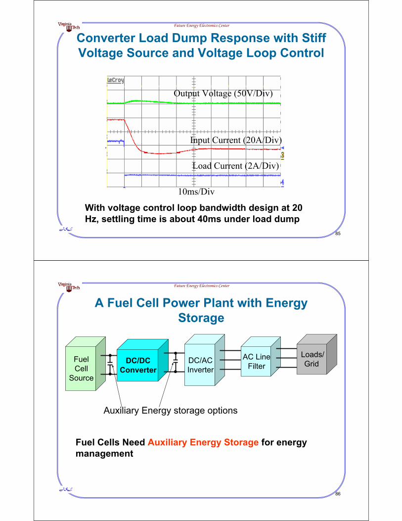
Converter Load Dump Response with Stiff Voltage Source and Voltage Loop Control
Load Current (2A/Div)
Output Voltage (50V/Div)
10ms/Div
Input Current (20A/Div)
With voltage control loop bandwidth design at 20 Hz, settling time is about 40ms under load dump
JSL86
Future Energy Electronics Center
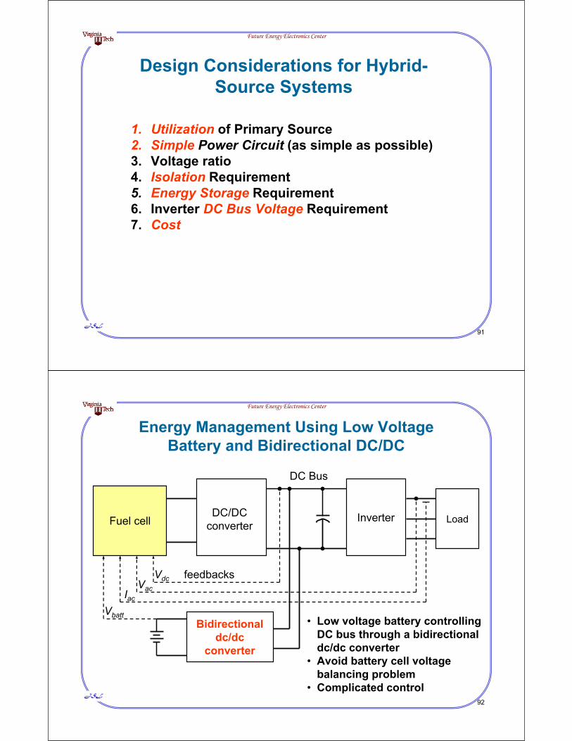
A Fuel Cell Power Plant with Energy Storage
FuelCell
Source
DC/DCConverter
DC/ACInverter
AC LineFilter
Loads/Grid
Auxiliary Energy storage options
Fuel Cells Need Auxiliary Energy Storage for energy management

JSL87
Future Energy Electronics Center
Low-Voltage Ultra-Capacitor Energy Storage Configuration
DC/DCconverter
48-72V
Ultra-capacitor
Fuel
Cel
l
120V
DC/ACInverter
Lf
JSL88
Future Energy Electronics Center
Use High-Voltage Battery as the Auxiliary Energy Storage
FuelCell
Source
DC/DCConverter
ACLoad
High voltage auxiliary energy storage battery
Capacitorfilter
120V
Photographof a 96V battery bank
fuse

JSL89
Future Energy Electronics Center
Potential Problems with Passive Energy Storage
• Low-side ultracap option:– Two voltage sources are paralleled – not a good
engineering practice – Time to reach equilibrium point is too long because
dynamic characteristics of both sources are different– Ultra capacitor helps transient current sharing, but
creates significant voltage and current ripples due to interaction between two voltage sources
– Dynamic current sharing problem• High-side battery option:
– Battery cell voltage balance problem – Battery state-of-charge management – Long-term battery life expectancy – Cost of battery is a concern
JSL90
Future Energy Electronics Center
Energy Management Options with Energy Storages and Power Electronics
• Optimum energy usage control • Start-up control• Load transient control • Charging and discharging (bidirectional) controls
for auxiliary energy storages
JSL91
Future Energy Electronics Center
Design Considerations for Hybrid-Source Systems
1. Utilization of Primary Source2. Simple Power Circuit (as simple as possible)3. Voltage ratio4. Isolation Requirement5. Energy Storage Requirement6. Inverter DC Bus Voltage Requirement7. Cost
JSL92
Future Energy Electronics Center
Energy Management Using Low Voltage Battery and Bidirectional DC/DC
Fuel cell LoadDC/DCconverter
Inverter
DC Bus
Vdc
Iac
feedbacks
Bidirectionaldc/dc
converter
Vac
Vbatt • Low voltage battery controlling DC bus through a bidirectional dc/dc converter
• Avoid battery cell voltage balancing problem
• Complicated control

JSL93
Future Energy Electronics Center
Dual-Source Energy Management Using a Unidirectional Boost Converter
AB
C
100kW Inverter
+
+
–
300 V
–
D2
S1
VdcAC
Output
L1
Low voltageFuel cell
High voltagebattery
• Battery voltage > Fuel cell voltage• Simple boost converter regulates the battery state of charge• DC bus voltage is constant
180–
240
V
Fuel
Cel
l
80kW converter
Total power electronics: 80-kW DC/DC + 100-kW DC/ACTotal energy sources: 20-kW battery + 80-kW fuel cell
JSL94
Future Energy Electronics Center
An Example of Dual Sources with a Bidirectional DC-DC Converter
AB
C
100kW Inverter
+
+
– 240–
380
V
180–
240
V
–
S1
S2
VdcAC
Output
Battery voltage < fuel cell voltage needs a boost converter to supply energy during transient load and a buck converter to charge the battery
Fuel cell voltage = dc bus voltage not regulated
L1
LowvoltageBattery
High voltageFuel cell
Fuel
Cel
l
20kW Converter
• Total power electronics: 20-kW DC/DC + 100-kW DC/AC• Total energy sources: 20-kW battery + 80-kW fuel cell

JSL95
Future Energy Electronics Center
Interleaved Bidirectional DC/DC Converter forFuel Cell Energy Management
Ld1
Ld2
S1u S2u
S1d S2d
VFC
Vbatt
Fuel
Cel
l 100 kWInverter
20kW converter
• Total power electronics: 20-kW DC/DC + 100-kW DC/AC• Total energy sources: 20-kW battery + 80-kW fuel cell
80kW
20kW
Interleaved operation for both boost and buck modes • smaller passive components; • less battery ripple current
JSL96
Future Energy Electronics Center
DC Bus Voltage During 800-W Load Step and Load Dump Under Boost Mode Operation
VdcVdc
Idc (1A/div)
(50V/div)(50V/div)
Idc (1A/div)
DC bus voltage fluctuates but returns to original setting after load transients
20ms/div 20ms/div
JSL97
Future Energy Electronics Center
Battery Voltage During 800-W Battery Charge Command Step under Buck Mode Operation
Vbatt
Idc (2A/div)
(20V/div)
(20A/div)ILd1
Vbatt
Idc (2A/div)
(20V/div)
(20A/div)ILd1
Battery voltage keeps constant during severe charging and discharging current conditions
JSL98
Future Energy Electronics Center
8. Advanced V6 Converter
• Single-Phase Half-Bridge Converter• Two-Phase Full-bridge Converter• Three-Phase Converter• V6 Converter• Test Results with V6 Converter• V6 Converter Prototype
JSL99
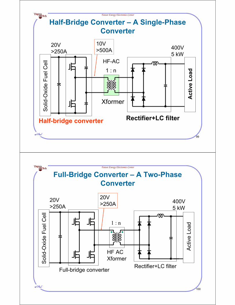
Future Energy Electronics Center
Half-Bridge Converter – A Single-Phase Converter
1 : nHF-AC
Half-bridge converter
Xformer
Rectifier+LC filter
Act
ive
Load
20V>250A
Sol
id-O
xide
Fue
l Cel
l400V5 kW
10V>500A
JSL100
Future Energy Electronics Center
Full-Bridge Converter – A Two-Phase Converter
1 : n
HF ACXformer
Rectifier+LC filter
Act
ive
Load
Sol
id-O
xide
Fue
l Cel
l
Full-bridge converter
20V>250A
400V5 kW
20V>250A

JSL101
Future Energy Electronics Center
Full-Bridge Converter with Paralleled Devices to Achieve Desired Power Levels
Load6x 6x
• With 6 devices in parallel, the two-leg converter can barely achieve 95% efficiency
• Problems are additional losses in parasitic components, voltage clamp, interconnects, filter inductor, transformer, diodes, etc.
Voltage clampSol
id-O
xide
Fue
l Cel
l20V250A
JSL102
Future Energy Electronics Center
Fuel Cell Voltage and Current with Full Bridge Converter Case
Time
0s 2ms 4ms 6ms 8ms 10msV(Vfc)
10V
20V
30V
-I(Vfc)20A
40A
60A
I(Cin)-50A
50A
100A
150A
SEL>>
I(Ld3) V(Iac)-15A
-5A
5A
15A
Fuel cell voltage
Fuel cell currentLoad step
Input capacitor current
AC load currentFilter inductor current
Load dump
330%
33%
JSL103
Future Energy Electronics Center
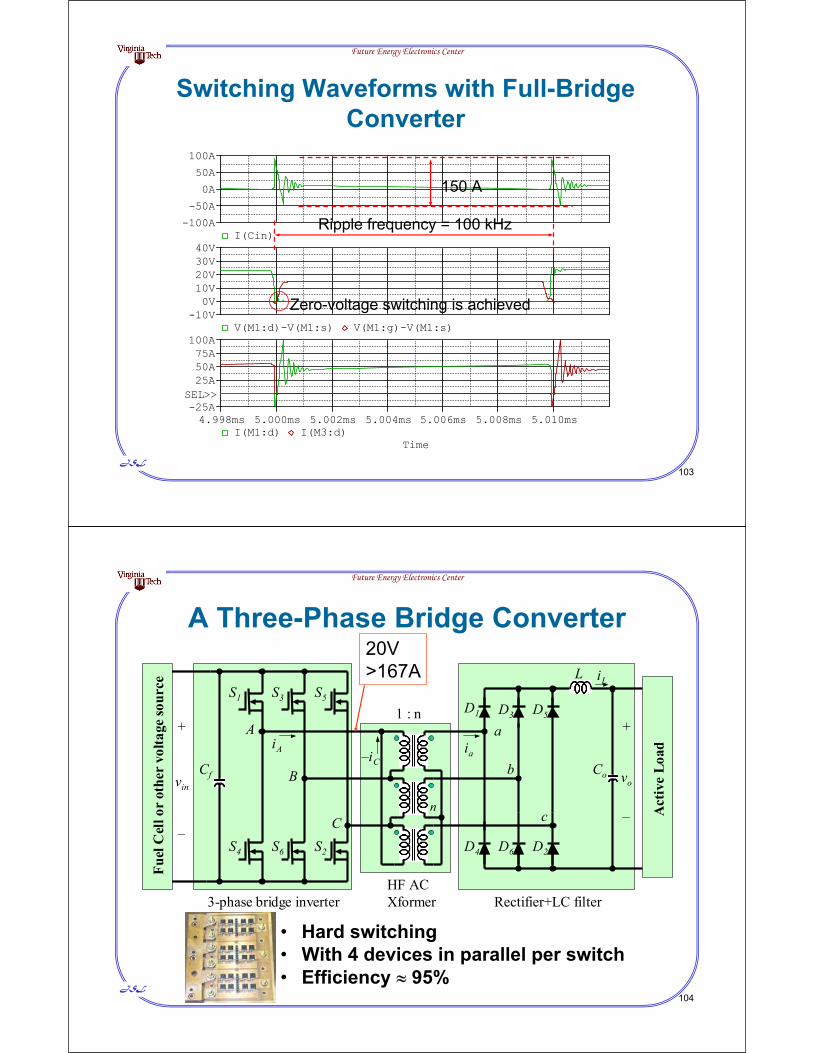
Switching Waveforms with Full-Bridge Converter
Time
4.998ms 5.000ms 5.002ms 5.004ms 5.006ms 5.008ms 5.010msI(M1:d) I(M3:d)
-25A
25A50A75A100A
SEL>>
V(M1:d)-V(M1:s) V(M1:g)-V(M1:s)-10V0V10V20V30V40V
I(Cin)-100A
-50A
0A
50A
100A
150 A
Ripple frequency = 100 kHz
Zero-voltage switching is achieved
JSL104
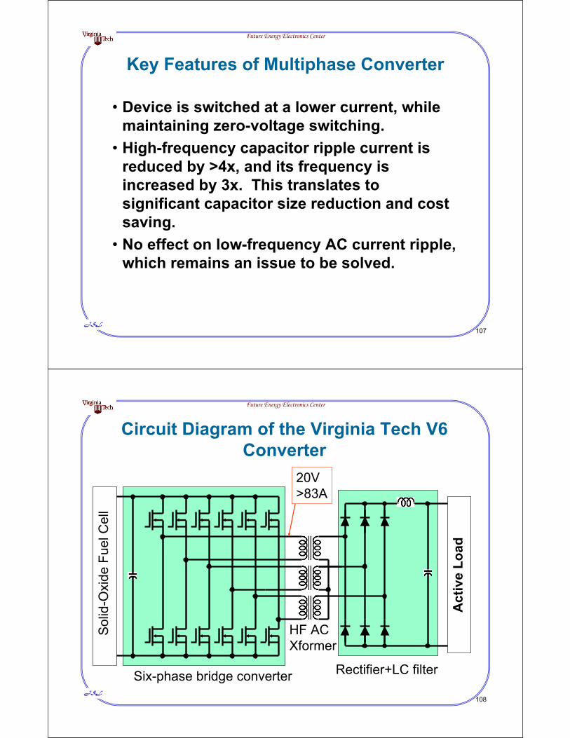
Future Energy Electronics Center
A Three-Phase Bridge Converter
vin
L
Cf
+
–
Co vo
+
–
1 : nS1 S5
S4 S2
a
c
HF ACXformer Rectifier+LC filter
D1
D4
D3
D6
iA ia
iL
Act
ive
Load
Fuel
Cel
l or o
ther
vol
tage
sour
ce
3-phase bridge inverter
S3
S6
b
D5
D2
A
B
Cn
–iC
• Hard switching • With 4 devices in parallel per switch• Efficiency 95%
20V>167A

JSL105
Future Energy Electronics Center
Fuel Cell Voltage and Current with 3-Phase Bridge Converter Case
Time
0s 5ms 10msV(Vfc)
10V
20V
30V
-I(Vfc)20A
60A
SEL>>
I(Cin)-50A
0A
50A
100A
150AI(Ld3) V(Iac)
-15A
-5A
5A
15A
Fuel cell voltage
Fuel cell currentLoad step
Input capacitor current
AC load currentFilter inductor current
A significant reduction in capacitor ripple current
33%
80%
No reduction in low-freq. fuel cell ripple current
Load dump
JSL106
Future Energy Electronics Center
Switching Waveforms with 3-Phase Bridge Converter
Time
4.998ms 5.000ms 5.002ms 5.004ms 5.006ms 5.008ms 5.010msI(M1:d) I(M4:d)
-25A0A
25A50A75A
100AV(M1:d)-V(M1:s) V(M1:g)-V(M1:s)
-10V0V
10V20V30V40V
I(Cin)-50A
0A
25A
50A
SEL>> 35 A
Ripple frequency = 300 kHz
Zero-voltage switching is achieved
JSL107
Future Energy Electronics Center
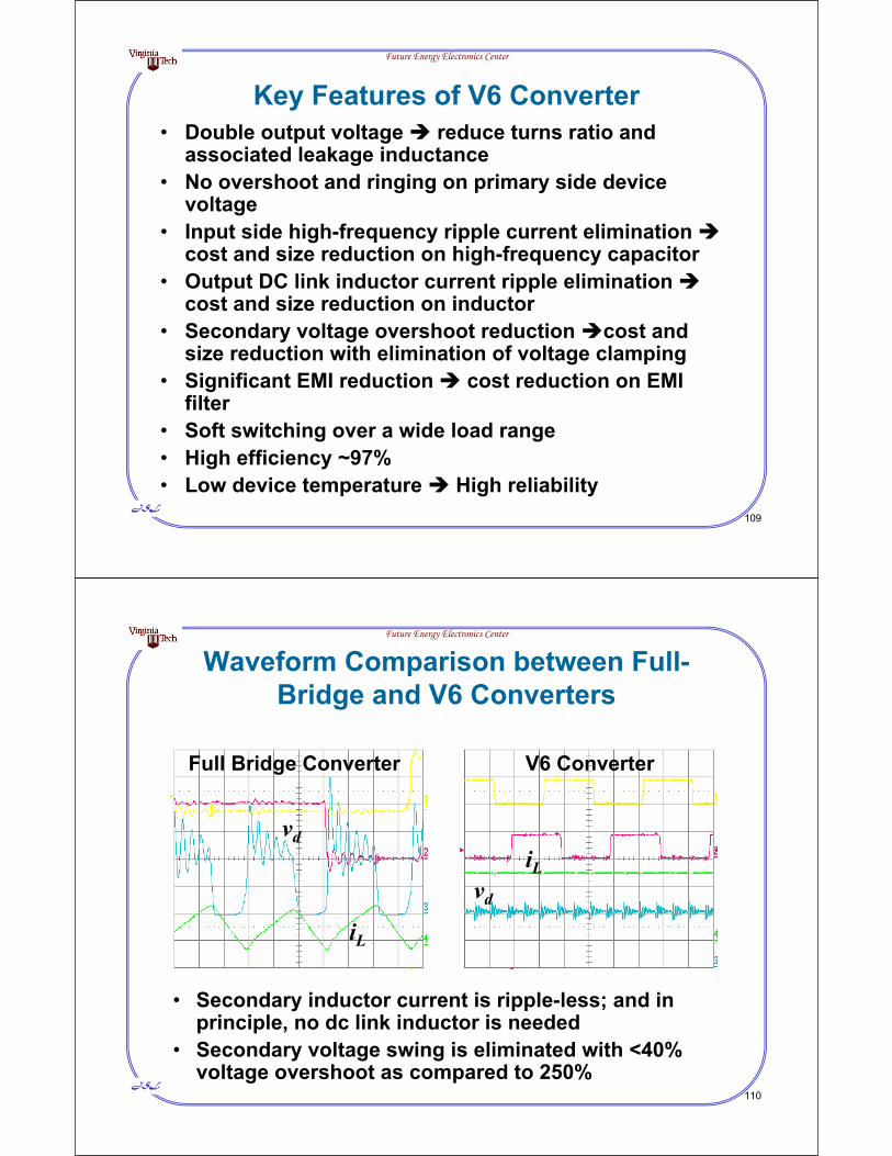
Key Features of Multiphase Converter
• Device is switched at a lower current, while maintaining zero-voltage switching.
• High-frequency capacitor ripple current is reduced by >4x, and its frequency is increased by 3x. This translates to significant capacitor size reduction and cost saving.
• No effect on low-frequency AC current ripple, which remains an issue to be solved.
JSL108
Future Energy Electronics Center
Circuit Diagram of the Virginia Tech V6 Converter
Sol
id-O
xide
Fue
l Cel
l
Act
ive
Load
Rectifier+LC filterSix-phase bridge converter
HF ACXformer
20V>83A
JSL109
Future Energy Electronics Center
Key Features of V6 Converter• Double output voltage reduce turns ratio and
associated leakage inductance• No overshoot and ringing on primary side device
voltage• Input side high-frequency ripple current elimination
cost and size reduction on high-frequency capacitor• Output DC link inductor current ripple elimination
cost and size reduction on inductor • Secondary voltage overshoot reduction cost and
size reduction with elimination of voltage clamping• Significant EMI reduction cost reduction on EMI
filter• Soft switching over a wide load range• High efficiency ~97% • Low device temperature High reliability
JSL110
Future Energy Electronics Center
Waveform Comparison between Full-Bridge and V6 Converters
Full Bridge Converter V6 Converter
iL
iL
vd
vd
• Secondary inductor current is ripple-less; and in principle, no dc link inductor is needed
• Secondary voltage swing is eliminated with <40% voltage overshoot as compared to 250%
JSL111
Future Energy Electronics Center
Significant DC link Inductor Size Reduction
With V6 converter, an effective 10x reduction in DC link filter inductor in terms of cost, size and weight
Single Phase500W60Hz
Single Phase5 kW50kHz
Three Phase5 kW50kHz
Single Phase500W60Hz
Single Phase5 kW50kHz
Three Phase5 kW50kHz
Single Phase500W60Hz
Single Phase5 kW50kHz
Three Phase5 kW50kHz
JSL112
Future Energy Electronics Center
Input and Output Voltages and Currents at 1kW Output Condition
Vin
VoVo
Iin
Vin
Iin
Io
Io
(a) Full bridge converter (b) V6 Converter
Significant improvement with V6 converterLess EMIBetter efficiency (97% versus 87% after calibration)
(97%)(87%)

JSL113
Future Energy Electronics Center
Where are the Losses?• Switch conduction • Diode conduction • Transformer• Output rectifier • Output filter inductor and capacitor• Input capacitor• Parasitics
– Copper traces– Interconnects
JSL114
Future Energy Electronics Center
Calorimetry for Accurate Loss Measurement
Calibration with resistor bank
fans

JSL115
Future Energy Electronics Center
Test the 160-Liter Calorimeter at 120-W Loss Condition
0102030405060708090
0 100 200 300 400 500 600Time (min)
Tem
pera
ture
(deg
C)
Average probe temperature
Temperature rise
>9 hours for each test points
JSL116
Future Energy Electronics Center
Temperature Rise Versus Power Loss
y = 0.4086x + 2.9771
1520253035404550556065
30 40 50 60 70 80 90 100 110 120 130Power Loss (W)
Tem
pera
ture
(deg
C)
TempRise
Linear (TempRise)

JSL117
Future Energy Electronics Center
Efficiency Measurement Results
80%82%84%86%88%90%92%94%96%98%
100%
0 1000 2000 3000 4000Output power (W)
Experimental data and trend line
• Measurement error: within 1%• Heat sink temperature rise:
<20°C at 2kW with natural convection
Effi
cien
cy
75%
80%
85%
90%
95%
100%
0 500 1000 1500 2000 2500Output Power (W)
Effic
ienc
yPhase-II V6-Converter Efficiency (calibrated)
Phase-I Efficiency Measured Results
JSL118
Future Energy Electronics Center
The Beta Version Prototype Converter
• Schematic Circuit Diagrams• V6 Cost Estimate • Summary of Beta Version Prototype

JSL119
Future Energy Electronics Center
Schematic Circuit Diagrams
Power boardGate drive board
Control boardDigital board
Interface board
JSL120
Future Energy Electronics Center
Photographs of V6-Converter Together with DC-AC Inverter Prototype
Front View Rear View
ConverterInverter

JSL121
Future Energy Electronics Center
Prototype and Production Cost Estimate for the 5-kW V6 DC-DC Converter
Quantity 100 1000 10000Material cost $475 $347 $227Tooling, Assembly & Testing $1,424 $347 $114Production Cost $1,899 $694 $341
Key Materials Parts Count Qty 1 Qty 10000Power Circuit 22 $571.00 $154.40 Devices 8 $201.00 $38.40 Capacitors 6 $84.00 $30.00 Transformers 3 $180.00 $45.00 Inductors 2 $24.00 $8.00 Sensors 2 $32.00 $8.00 Contactor 1 $50.00 $25.00Control Circuit 325 $113.70 $33.22 Resistors 164 $18.59 $2.71 Capacitors 110 $46.61 $17.41 Discretes 27 $8.00 $2.42 IC's 24 $40.50 $10.68Miscellaneous 55 $174.80 $52.44Total 402 $840.50 $227.05
JSL122
Future Energy Electronics Center
9. Fuel Cell Current Ripple Issues
Lf
Cf RA
BVdc
+
–
Sap
San Sbn
Sbp
Vo
+
–
60Hz
120Hz
• Current ripple propagates from AC load back to DC side• With rectification, ripple frequency is 120 Hz for 60 Hz
systems• Low-frequency ripple is difficult to be filtered unless
capacitor is large enough
AC filter LC
High-sidecap.
DC-DCconverter
120Hz
FuelCell

JSL123
Future Energy Electronics Center
AC Current Ripple Problems
• Inverter AC current ripple propagates back to fuel cell • Fuel cell requires a higher current handling capability
Cost penalty to fuel cell stack• Ripple current can cause hysteresis losses and
subsequently more fuel consumption Cost penalty to fuel consumption
• State-of-the-art solutions are adding more capacitors or adding an external active filters Size and cost penalty
• Virginia Tech solution is to use existing V6 converter with active ripple cancellation technique to eliminate the ripple No penalty
JSL124
Future Energy Electronics Center
Circuit Model for AC Current Ripple
N:1Iin
Vin Iload
RsLf
Vdc
+
–
Ip Is
iin/N
iload
N2RsLfip/N is
DC Model
AC Ripple ModelCin/N2
N2RCin
Cin
RCin
Cf
RCf
Cf
RCf
DC/DCConverterVin
Rs Lf
IloadCin
RCin
Cf
RCf

JSL125
Future Energy Electronics Center
Solutions to Ripple Currents
• Add more capacitors (ultra capacitor) on the low-side dc bus
• Add more capacitors on the high-side dc bus
• Add one more stage DC-DC converter • Add an active ripple cancellation circuit
– with a bidirectional DC-DC converter to stabilize the high-side dc bus voltage
– with a built-in control function in the DC-DC converter
JSL126
Future Energy Electronics Center
Benchmark DC/DC Converter Parameters for Ripple Study
• Input Voltage: 25V• Output Voltage: 200V• Input DC Capacitor: 6mF• Output DC Capacitor: 2200mF• Filter Inductor: 84mH• Inverter Modulation Index: 0.86• Inverter Load Resistor: 16.7

JSL127
Future Energy Electronics Center
Adding Hide-Side Energy Storages on DC Bus Helps Reduce Ripple Current
0.25k
-50
0.1k
0 50m10m 20m 30m 40m0.25k
-50
0.1k
0 50m10m 20m 30m 40mTime (s)
20% ripple current
10% ripple current
DC/DCConverter
DC bus energy buffer
4-cycle energy backup
8-cycle energy backup
ACLoad
120VFuelCell
JSL128
Future Energy Electronics Center
Simulation Results with LV-Side Capacitor Input Capacitor has Very Little Effect to Current
Ripple Reduction
t(s)0 0.01 0.02 0.03 0.04 0.05
0
1015
5
200
19080
40
0
20
25
(A)
(V)
(A)
(V)
HV DCCurrent
HV DCVoltage
LV DCVoltage
LV DCCurrent
t(s)0 0.01 0.02 0.03 0.04 0.05
0
1015
5
200
19080
40
0
20
25
(A)
(V)
(A)
(V)
Input Cap Reduced to 136 FInput Cap 6mF
JSL129
Future Energy Electronics Center
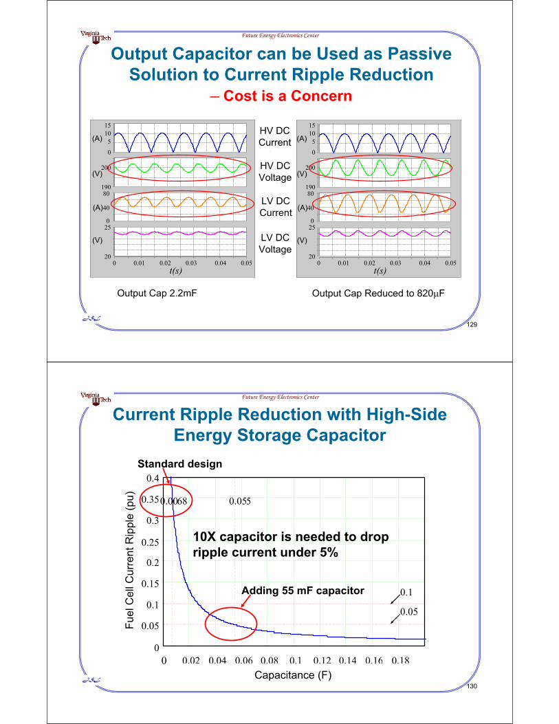
Output Capacitor can be Used as Passive Solution to Current Ripple Reduction
– Cost is a Concern
t(s)0 0.01 0.02 0.03 0.04 0.05
0
1015
5
200
19080
40
0
20
25
(A)
(V)
(A)
(V)
HV DCCurrent
HV DCVoltage
LV DCVoltage
LV DCCurrent
t(s)0 0.01 0.02 0.03 0.04 0.05
0
1015
5
200
19080
40
0
20
25
(A)
(V)
(A)
(V)
Output Cap Reduced to 820 FOutput Cap 2.2mF
JSL130
Future Energy Electronics Center
Current Ripple Reduction with High-Side Energy Storage Capacitor
1 10 4 0.02 0.04 0.06 0.08 0.1 0.12 0.14 0.16 0.180
0.05
0.1
0.15
0.2
0.25
0.3
0.35
0.4
0.05
0.1
0.0068 0.055
Capacitance (F)
Fuel
Cel
l Cur
rent
Rip
ple
(pu)
0
Standard design
Adding 55 mF capacitor
10X capacitor is needed to drop ripple current under 5%

JSL131
Future Energy Electronics Center
Features of High-Voltage DC Bus Energy Storage Capacitors
• Fuel cell voltage is low, typically from 36 to 60 V.• High voltage dc bus voltage is split into two 200 V.• For a single-phase dual ac outputs such as 120/240 V in US
residential systems, the transformer secondary and dc bus can be split in two halves. Each phase leg of the full-bridge along with the split-capacitors becomes a half-bridge inverter to supply 120 V ac output. Summing two 120 V outputs becomes 240 V.
• Multiple capacitors are paralleled for the high-voltage dc bus to store more energy and to provide more transient handling capability during dynamic load change conditions. Energy storage is proportional to CV2.
• Size and weight are dominated by passive components. With split DC buses, the volume of energy storage capacitors becomes an issue.
JSL132
Future Energy Electronics Center
Experimental Current Ripples without Adding Capacitors or Controls
Fuel cell voltage (20V/div)
Fuel cell current (10A/div)
AC Load Voltage (200V/div)AC Load Current (5A/div)
5ms/div
More than 35% ripple current at the input
35%

JSL133
Future Energy Electronics Center
Fuel Cell Ripple Current Problem is Severe During Load Transients
• For single-phase ac loads, 120 Hz (twice the fundamental frequency) current ripple can reflect back to fuel cell.
• During load transients such as turning on light bulbs or starting up motors, the transient initial current is typically more than 5 times the steady-state current, and the fuel cell ripple current exceeds more 100% or even 200% in some cases.
JSL134
Future Energy Electronics Center
Fuel Cell Responds to AC Load Steps (without Externally Added Capacitor)
Ifc
Vfc
iac
Fuel Cell Voltage (10V/div)
Fuel Cell Current (10A/div)
DC Link Current (25A/div)
AC Load Current (10A/div)20ms/div
Id-LV
Fuel cell sees severe current transient (spike) and current ripple in steady state (35%)
JSL135
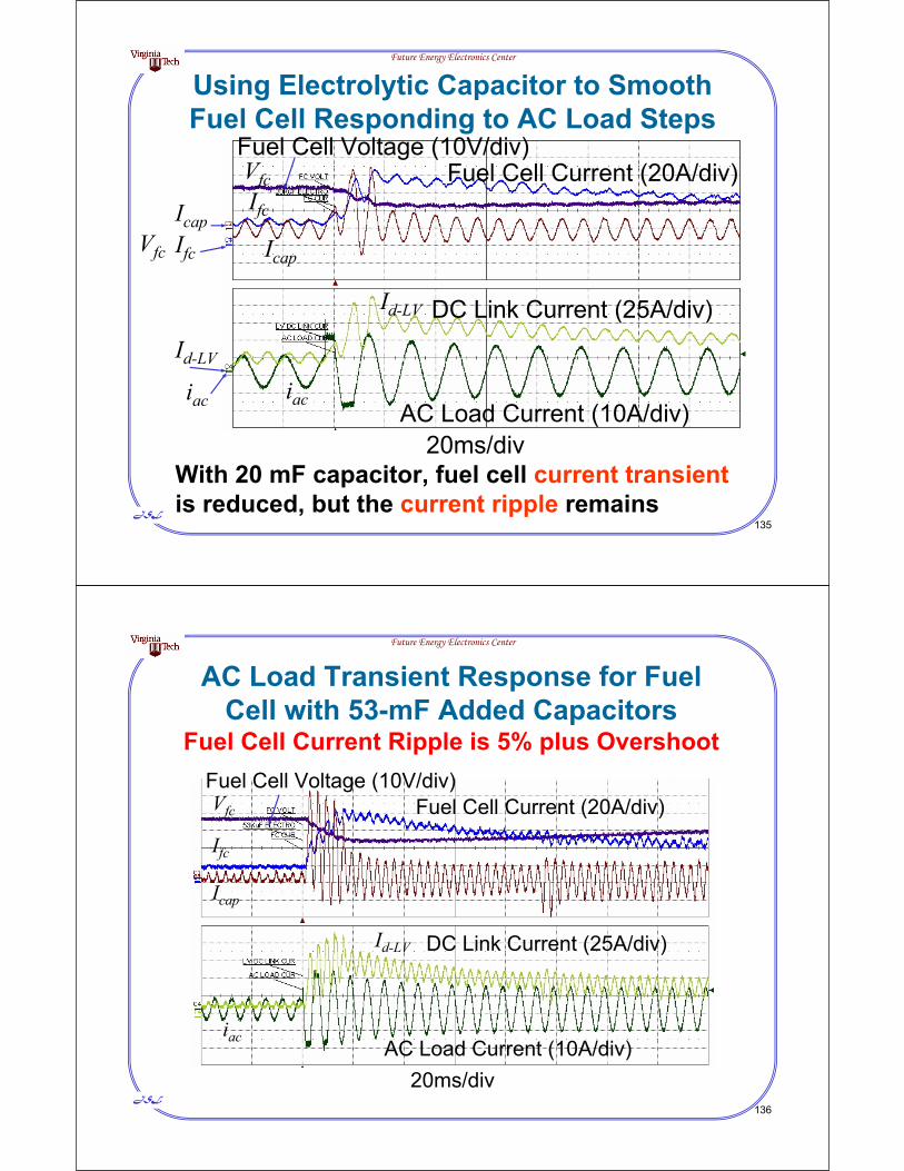
Future Energy Electronics Center
Using Electrolytic Capacitor to Smooth Fuel Cell Responding to AC Load Steps
Ifc
Vfc
iac
Fuel Cell Voltage (10V/div)Fuel Cell Current (20A/div)
DC Link Current (25A/div)
AC Load Current (10A/div)20ms/div
Id-LV
IcapIfc
iac
IcapVfc
Id-LV
With 20 mF capacitor, fuel cell current transient is reduced, but the current ripple remains
JSL136
Future Energy Electronics Center
AC Load Transient Response for Fuel Cell with 53-mF Added Capacitors
Fuel Cell Current Ripple is 5% plus Overshoot
Vfc
Fuel Cell Voltage (10V/div)Fuel Cell Current (20A/div)
DC Link Current (25A/div)
AC Load Current (10A/div)20ms/div
Ifc
iac
Icap
Id-LV
JSL137
Future Energy Electronics Center
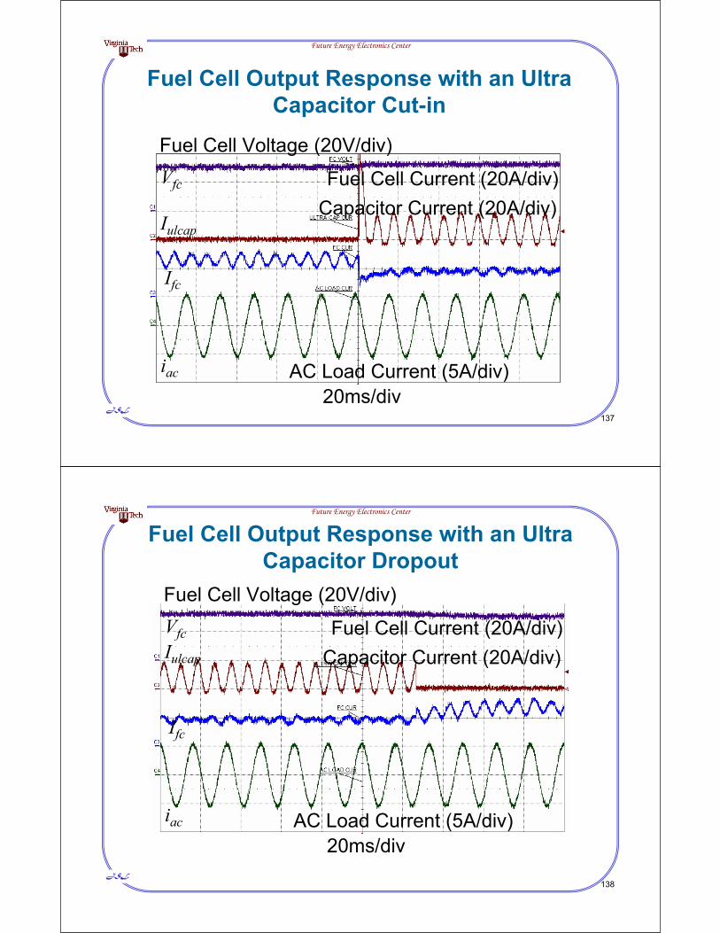
Fuel Cell Output Response with an Ultra Capacitor Cut-in
Vfc
Fuel Cell Voltage (20V/div)
Fuel Cell Current (20A/div)
AC Load Current (5A/div)20ms/div
Ifc
iac
IulcapCapacitor Current (20A/div)
JSL138
Future Energy Electronics Center
Fuel Cell Output Response with an Ultra Capacitor Dropout
Vfc
Fuel Cell Voltage (20V/div)
Fuel Cell Current (20A/div)
AC Load Current (5A/div)20ms/div
Ifc
iac
Iulcap Capacitor Current (20A/div)

JSL139
Future Energy Electronics Center
Experiment with Open-Loop and with only Voltage Loop Control
No improvement on current ripple reduction with voltage loop control
DC bus voltage (100V/div)
Fuel cell voltage (10V/div)
Fuel cell current (20A/div)
DC bus current (10A/div)
(a) Open loop (b) With voltage loop control
t (5ms/div)
JSL140
Future Energy Electronics Center
Solving Current Ripple with Added Current Loop inside the Voltage Loop
vref +–
Rv2Cv1
Cv2
Rv1
Hv
vsense
Vo
+RL
Gvc
+–
Vm
PWMd
Lf
Cf
VdiLf
+–
Rcf+–
Ri2Ci1
Hi
iref
Ri1
isense
Ci2
Gic Vd = dVin
Adding a current loop to regulate the output current

JSL141
Future Energy Electronics Center
Fuel Cell Current Ripple Reduction with the Proposed Active Control Technique
Fuel Cell Current Ripple is Reduced to 2%
Input Voltage
Input Current
Output Current
Output Voltage
<2%
JSL142
Future Energy Electronics Center
Summary of V6 DC-DC Converter with Active Ripple Cancellation
• High efficiency with a wide-range soft switching: 97%• Cost reduction by cutting down passive components
– Output inductor filter reduction with three-phase interleaved control: 6X
– Input high frequency capacitor reduction: 6X– Output capacitor reduction with active ripple reduction: 10X
• Reliability enhancement– No devices in parallel– Soft-start control to limit output voltage overshoot – Current loop control to limit fuel cell inrush currents
• Significance to SOFC design – Stack size reduction by efficient power conversion and ripple
reduction: 20%– Inrush current reduction for reliability enhancement
JSL143
Future Energy Electronics Center
10. Recap
1. Basic DC-DC converters and DC-AC inverters are introduced
2. Circuit topology selection can be misled by schematic diagram. Some important considerations are• Device voltage and current stresses• Number of paralleled devices • Parasitic components and losses
3. Advanced V6 DC-DC converter not only shows superior performance but also low production cost
4. Fuel cell current ripple issue can now be solved with advanced current control developed by Virginia Tech without adding cost penalty