Porous Doped Silicon Nanowires for Lithium Ion Battery Anode … · 2018-03-05 · Porous Doped...
6
Porous Doped Silicon Nanowires for Lithium Ion Battery Anode with Long Cycle Life Mingyuan Ge, †,§ Jiepeng Rong, †,§ Xin Fang, † and Chongwu Zhou* ,‡ † Department of Electrical Engineering and ‡ Department of Chemical Engineering and Materials Science, University of Southern California, Los Angeles, California 90089, United States * S Supporting Information ABSTRACT: Porous silicon nanowires have been well studied for various applications; however, there are only very limited reports on porous silicon nanowires used for energy storage. Here, we report both experimental and theoretical studies of porous doped silicon nanowires synthesized by direct etching of boron-doped silicon wafers. When using alginate as a binder, porous silicon nanowires exhibited superior electrochemical performance and long cycle life as anode material in a lithium ion battery. Even after 250 cycles, the capacity remains stable above 2000, 1600, and 1100 mAh/g at current rates of 2, 4, and 18 A/g, respectively, demonstrating high structure stability due to the high porosity and electron conductivity of the porous silicon nanowires. A mathematic model coupling the lithium ion diffusion and the strain induced by lithium intercalation was employed to study the effect of porosity and pore size on the structure stability. Simulation shows silicon with high porosity and large pore size help to stabilize the structure during charge/discharge cycles. KEYWORDS: Porous silicon nanowire anode, structure stability, alginate binder, high current rate T he ever increasing demand in energy storage has stimulated significant interest in lithium ion battery research. The lithium ion battery is one of the most promising systems which is efficient in delivering energy, light in weight, and environmentally benign. 1−5 Existing lithium ion batteries using graphite as the anode have already been widely used in mobile applications; however, it is still urgent and important to develop new battery systems with larger specific capacity and higher power density for applications in mobile devices, hybrid electric vehicles (HEVs), and plug-in hybrid electric vehicles (PHEVs). 6 For anode materials, silicon is known to have the highest theoretical specific capacity (4200 mAh/g). 7 Compar- ing with graphite (372 mAh/g), which is currently used, silicon is considered to be the anode material for the next generation lithium ion batteries. However, silicon is easy to pulverize and loses its capacity due to large volume change (around 300%) during repeated insertion and extraction of lithium ions. 8 In addition, silicon has low electron conductivity (when undoped) and low diffusivity for lithium ions. The above-mentioned drawbacks set hindrances for silicon to be used in high power density batteries. Decreasing the silicon dimensions to submicrometers or nanometers, to a large extent, solves the problems mentioned above. Extensive studies on silicon thin films, 9,10 silicon nanowires, 11−14 nanoparticles, 15,16 nano- tubes, 17−19 and porous structures 20−23 have shown very encouraging results when used as anode materials in lithium ion batteries. For half cells, which use silicon as the working electrode and lithium metal as the counter electrode, the battery voltage is determined by the chemical potential difference of lithium ions at the interface between electrolyte and silicon. The charge process finishes when the lithium-rich phase (Li 22 Si 5 at high temperature and Li 15 Si 4 at room temperature) 24 is formed at the silicon surface, and the discharge process ends when all the lithium ions are extracted from the very outer surface of silicon, regardless of whether the inner part of silicon has fully participated in the lithiation/delithiation process or not. The charge/discharge capacities are related to both the transfer of lithium ions between the electrolyte and silicon interface and the diffusion of lithium ions inside silicon. This explains why usually only a portion of the theoretical capacity can be reached, and the problem of reduced capacity gets exacerbated when the battery runs at a higher charge/discharge rate. Therefore, obtaining uniform lithium ion concentration in silicon at a fast charge/discharge rate remains a challenge to be addressed. In addition, at very high charge/discharge rates, low electron conductivity of intrinsic silicon would also compromise battery performance and result in reduced capacity. To enable silicon to work at high charge/discharge rates, it is therefore very important to have the following properties: a large surface area accessible to the electrolyte, a short diffusion length for lithium ions, a large space available to accommodate volume change, and a high electron conductivity. Here we report both the experimental and the theoretical study of porous doped silicon nanowires synthesized by direct etching of boron-doped silicon wafers. The obtained porous Received: January 17, 2012 Revised: April 2, 2012 Published: April 9, 2012 Letter pubs.acs.org/NanoLett © 2012 American Chemical Society 2318 dx.doi.org/10.1021/nl300206e | Nano Lett. 2012, 12, 2318−2323
Transcript of Porous Doped Silicon Nanowires for Lithium Ion Battery Anode … · 2018-03-05 · Porous Doped...
Porous Doped Silicon Nanowires for Lithium Ion Battery Anode withLong Cycle LifeMingyuan Ge,†,§ Jiepeng Rong,†,§ Xin Fang,† and Chongwu Zhou*,‡
†Department of Electrical Engineering and ‡Department of Chemical Engineering and Materials Science, University of SouthernCalifornia, Los Angeles, California 90089, United States
*S Supporting Information
ABSTRACT: Porous silicon nanowires have been well studied forvarious applications; however, there are only very limited reports onporous silicon nanowires used for energy storage. Here, we reportboth experimental and theoretical studies of porous doped siliconnanowires synthesized by direct etching of boron-doped siliconwafers. When using alginate as a binder, porous silicon nanowiresexhibited superior electrochemical performance and long cycle lifeas anode material in a lithium ion battery. Even after 250 cycles, thecapacity remains stable above 2000, 1600, and 1100 mAh/g at current rates of 2, 4, and 18 A/g, respectively, demonstrating highstructure stability due to the high porosity and electron conductivity of the porous silicon nanowires. A mathematic modelcoupling the lithium ion diffusion and the strain induced by lithium intercalation was employed to study the effect of porosity andpore size on the structure stability. Simulation shows silicon with high porosity and large pore size help to stabilize the structureduring charge/discharge cycles.
KEYWORDS: Porous silicon nanowire anode, structure stability, alginate binder, high current rate
The ever increasing demand in energy storage hasstimulated significant interest in lithium ion battery
research. The lithium ion battery is one of the most promisingsystems which is efficient in delivering energy, light in weight,and environmentally benign.1−5 Existing lithium ion batteriesusing graphite as the anode have already been widely used inmobile applications; however, it is still urgent and important todevelop new battery systems with larger specific capacity andhigher power density for applications in mobile devices, hybridelectric vehicles (HEVs), and plug-in hybrid electric vehicles(PHEVs).6 For anode materials, silicon is known to have thehighest theoretical specific capacity (4200 mAh/g).7 Compar-ing with graphite (372 mAh/g), which is currently used, siliconis considered to be the anode material for the next generationlithium ion batteries. However, silicon is easy to pulverize andloses its capacity due to large volume change (around 300%)during repeated insertion and extraction of lithium ions.8 Inaddition, silicon has low electron conductivity (when undoped)and low diffusivity for lithium ions. The above-mentioneddrawbacks set hindrances for silicon to be used in high powerdensity batteries. Decreasing the silicon dimensions tosubmicrometers or nanometers, to a large extent, solves theproblems mentioned above. Extensive studies on silicon thinfilms,9,10 silicon nanowires,11−14 nanoparticles,15,16 nano-tubes,17−19 and porous structures20−23 have shown veryencouraging results when used as anode materials in lithiumion batteries.For half cells, which use silicon as the working electrode and
lithium metal as the counter electrode, the battery voltage isdetermined by the chemical potential difference of lithium ions
at the interface between electrolyte and silicon. The chargeprocess finishes when the lithium-rich phase (Li22Si5 at hightemperature and Li15Si4 at room temperature)24 is formed atthe silicon surface, and the discharge process ends when all thelithium ions are extracted from the very outer surface of silicon,regardless of whether the inner part of silicon has fullyparticipated in the lithiation/delithiation process or not. Thecharge/discharge capacities are related to both the transfer oflithium ions between the electrolyte and silicon interface andthe diffusion of lithium ions inside silicon. This explains whyusually only a portion of the theoretical capacity can bereached, and the problem of reduced capacity gets exacerbatedwhen the battery runs at a higher charge/discharge rate.Therefore, obtaining uniform lithium ion concentration insilicon at a fast charge/discharge rate remains a challenge to beaddressed. In addition, at very high charge/discharge rates, lowelectron conductivity of intrinsic silicon would also compromisebattery performance and result in reduced capacity. To enablesilicon to work at high charge/discharge rates, it is thereforevery important to have the following properties: a large surfacearea accessible to the electrolyte, a short diffusion length forlithium ions, a large space available to accommodate volumechange, and a high electron conductivity.Here we report both the experimental and the theoretical
study of porous doped silicon nanowires synthesized by directetching of boron-doped silicon wafers. The obtained porous
Received: January 17, 2012Revised: April 2, 2012Published: April 9, 2012
Letter
pubs.acs.org/NanoLett
© 2012 American Chemical Society 2318 dx.doi.org/10.1021/nl300206e | Nano Lett. 2012, 12, 2318−2323

silicon nanowires have all of the above properties. In addition,we used a commercially available alginic acid sodium salt as thebinder (denoted alginate binder), which has a viscosity of 2000cP at 2 wt % but so far has not been fully explored for batterystudy. The porous silicon nanowires exhibit superior electro-chemical performance and long cycle life as an anode materialin lithium ion batteries when combined with the alginatebinder. Even after 250 cycles, the capacity remains stable above2000, 1600, and 1100 mAh/g at current rates of 2, 4, and 18 A/g, respectively. Our best battery has recorded 2000 cycles with acapacity remaining above 1000 mAh/g. Simulation has beencarried out to illustrate strain induced by lithium ion diffusion,as stated below.A mathematic model25,26 coupling the lithium ion diffusion
and the strain induced by lithium intercalation was employed tostudy the effects of porosity and pore size on the structurestability. Figure 1a schematically shows the porous structure,and calculation and analysis were carried out on one unit(Figure 1b) of the structure in Figure 1a. Insertion of lithiumwould generate stress in the silicon matrix, and the straininduced by stress not only deforms the structure (expansion)but also compromises the lithium diffusion. The pore sizeevolution after lithium ion intercalation to Li22Si5 and Li15Si4 atfixed pore-to-pore distance (l = 12 nm) was presented in Figure1c. It shows that the pore diameter after lithium intercalationdecreases with decreasing initial pore size. The maximum stress
around the pore increases as we decrease the initial pore size(Figure 1d), which would act as a source of fracture. In anothercase, we fix the porosity by means of fixing the ratio of initialpore radius (r) and the pore-to-pore distance (l). Figure 1eshows the correlation of pore sizes before and after lithiation,and there is almost no change in the maximum stress atdifferent pore sizes (Figure 1f). Generally speaking, decreasingr/l ratio to a lower value (low porosity) would increasemaximum stress, and a smaller initial pore results in highermaximum stress around the pore. Therefore, obtaining siliconwith high porosity and large pore size would help to stabilizethe structure during the charge/discharge process. In order toverify the assumption, we synthesized porous silicon nanowireswith large pores to check their electrochemical performance.Porous Si nanowires were prepared according to previous
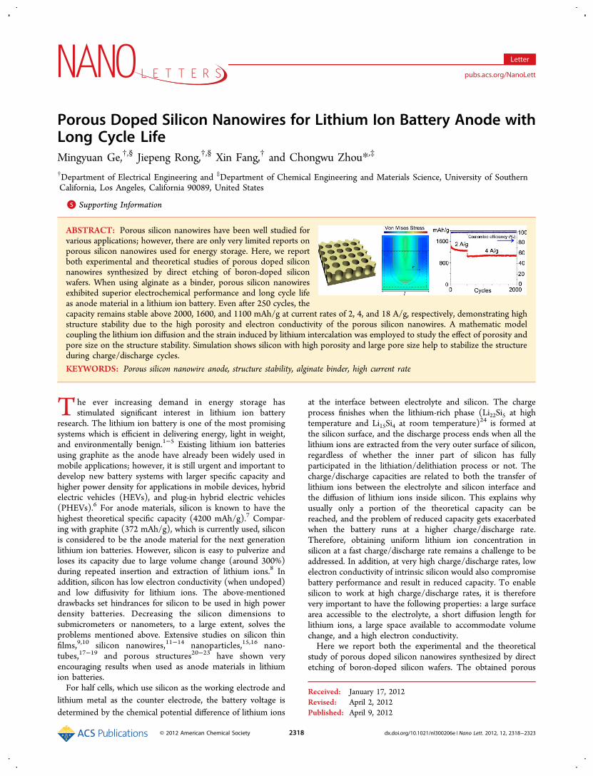
reports.27,28 Briefly, boron-doped Si wafers (resistivity <5mΩ·cm) were immersed in an etchant solution containing 5 Mhydrofluoric acid (HF) and 0.02 M silver nitrite (AgNO3) for 3h. Porous nanowires were washed by deionized water (DI-H2O), concentrated nitric acid (HNO3), and DI-H2O again,sequentially, and then collected by scratching the wafers using ablade. We note that doping is necessary for getting a porousstructure, and without doping, we can only get solid siliconnanowire. Figure 2 shows scanning electron microscopy (SEM)(Figure 2a) and transmission electron microscopy (TEM)(Figure 2b−d) images of porous Si nanowires. The nanowires
Figure 1. (a) Schematic diagram of a porous silicon structure. (b) One unit of the porous structure used for theoretical simulation and analysis. (c)Pore size before and after lithiation and (d) corresponding maximum stress at fixed pore-to-pore distance (l = 12 nm). (e) Pore size before and afterlithiation and (f) corresponding maximum stress vs initial pore size at fixed pore/edge ratio (r/l = 1/3).
Nano Letters Letter
dx.doi.org/10.1021/nl300206e | Nano Lett. 2012, 12, 2318−23232319
are highly porous at the surface, with pore diameter and wallthickness both around 8 nm (Figure 2b,c). The high-resolutionTEM (HRTEM) image in Figure 2d shows the nanowires arecrystalline with clear lattice fringes corresponding to a Si (111)lattice. The crystalline structure was also confirmed by the spotpattern in selected area electron diffraction (SAED) taken on asingle porous nanowire, as shown in Figure 2e. The pore sizecould be tailored by reacting with AgNO3 at differentconcentrations. Etchants containing 0.02 and 0.04 M AgNO3gave pores with mean diameters of 7.8 ± 0.1 and 10.5 ± 0.1 nm(Figure 2f), respectively, based on statistical analysis of theTEM images. The boron dopants provide defective sitesfacilitating the etching process which leaves holes on the siliconnanowire surface. The etching process was described as twosimultaneous electrochemical reactions:28
+ →+ −4Ag 4e 4Ag
+ → +− − −Si 6F [SiF ] 4e62
To test the electrochemical performance of porous siliconnanowires, two-electrode coin cells using porous siliconnanowires as the anode and lithium metal as the counterelectrode were fabricated. The Si mass loading is around 0.3mg/cm2, which is comparable to the amount previouslyreported for silicon nanowires.11 Figure 3a shows the voltageprofile in the charge (lithiation) and discharge (delithiation)
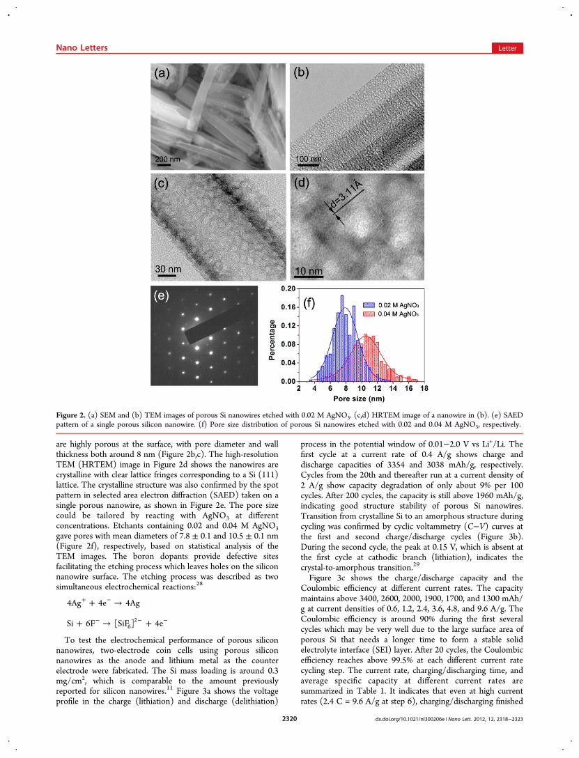
process in the potential window of 0.01−2.0 V vs Li+/Li. Thefirst cycle at a current rate of 0.4 A/g shows charge anddischarge capacities of 3354 and 3038 mAh/g, respectively.Cycles from the 20th and thereafter run at a current density of2 A/g show capacity degradation of only about 9% per 100cycles. After 200 cycles, the capacity is still above 1960 mAh/g,indicating good structure stability of porous Si nanowires.Transition from crystalline Si to an amorphous structure duringcycling was confirmed by cyclic voltammetry (C−V) curves atthe first and second charge/discharge cycles (Figure 3b).During the second cycle, the peak at 0.15 V, which is absent atthe first cycle at cathodic branch (lithiation), indicates thecrystal-to-amorphous transition.29
Figure 3c shows the charge/discharge capacity and theCoulombic efficiency at different current rates. The capacitymaintains above 3400, 2600, 2000, 1900, 1700, and 1300 mAh/g at current densities of 0.6, 1.2, 2.4, 3.6, 4.8, and 9.6 A/g. TheCoulombic efficiency is around 90% during the first severalcycles which may be very well due to the large surface area ofporous Si that needs a longer time to form a stable solidelectrolyte interface (SEI) layer. After 20 cycles, the Coulombicefficiency reaches above 99.5% at each different current ratecycling step. The current rate, charging/discharging time, andaverage specific capacity at different current rates aresummarized in Table 1. It indicates that even at high currentrates (2.4 C = 9.6 A/g at step 6), charging/discharging finished
Figure 2. (a) SEM and (b) TEM images of porous Si nanowires etched with 0.02 M AgNO3. (c,d) HRTEM image of a nanowire in (b). (e) SAEDpattern of a single porous silicon nanowire. (f) Pore size distribution of porous Si nanowires etched with 0.02 and 0.04 M AgNO3, respectively.
Nano Letters Letter
dx.doi.org/10.1021/nl300206e | Nano Lett. 2012, 12, 2318−23232320
within 10 min still gave capacity above 1300 mAh/g, equivalentto 38% of capacity using 0.15 C (step 1). Figure 3d shows along cycle performance at charging/discharging rate of 0.1 Cfor the first cycle and 0.5 C, 1 C, and 4.5 C for an additional250 cycles, which shows stable capacities around 2000, 1600,and 1100 mAh/g, respectively. Capacity degradation is almostnegligible in each case, demonstrating good stability of theporous silicon structure. The battery shown in the top panel ofFigure 3d has been retested with 0.5 C and then 1 C currentrate after one month. It shows that the capacity remains above1000 mAh/g after additional 2000 cycles (Figure 3e). Ourresult compares well with previously reported porous siliconstructures.20,21 As reported before, three-dimensional porous
silicon particles20 showed a capacity around 2500 mAh/g at acurrent rate of 0.5 C for 100 cycles, with Coulombic efficiency>98% at 0.5 C, while interconnected silicon hollow nano-spheres21 showed a capacity around 1400 mAh/g at a currentrate of 0.5 C for 700 cycles, with Coulombic efficiency >99.5%after 20 cycles. By comparison, we have reported the largestnumber of cycles (2000 cycles) with a capacity above 1000mAh/g. In addition, our preparation of porous siliconnanostructure does not require high-temperature annealing20
or chemical vapor deposition21 and therefore may offer apotential cost benefit.We note that a recent paper30 reported that silicon
nanoparticles (∼100 nm) can achieve good cyclability (100cycles) by using a special and possibly expensive alginate binder(viscosity >2000 cP at 1 wt %) synthesized in their own lab,and the authors attributed the improved cyclability to the highviscosity of their alginate binder. In contrast, here we used acommercially available alginate binder (Sigma Aldrich, cat. no.A2033) with lower viscosity (2000 cP at 2 wt %). We believethe significantly improved cyclability shown in Figure 3d,emainly stems from the use of a porous silicon structure, whilethe use of commercial alginate also helped to a certain degree ascompared to commonly used polyvinylidene fluoride (PVDF).Control experiments using commercial alginate binder on
Figure 3. Electrochemical performance of a battery using porous silicon nanowires as the anode and lithium metal as the current collector. (a)Charge/discharge profile within a voltage window of 0.01−2 V vs Li+/Li for the first cycle at a current rate of 0.4 A/g and the 50th, 100th, and 200thcycles at 2 A/g. (b) Cyclic voltammetry curves of porous silicon nanowire electrode for the first and second cycles using a voltage window 0.01−2 Vat rate of 0.1 mV/s. (c) Charge/discharge capacity and Coulombic efficiency of porous silicon nanowire electrode at current rates of 0.6, 1.2, 2.4, 3.6,4.8, and 9.6 A/g. (d) Charge/discharge capacity of a porous silicon nanowire electrode at current rates of 2, 4, and 18 A/g for 250 cycles. (e)Charge/discharge capacity of a porous silicon nanowire electrode at current rates of 2 A/g (0.5 C) and 4 A/g (1 C) with an additional 2000 cycles.
Table 1. Detailed Information of Battery PerformanceCorresponding to Figure 3c
stepnumber
numberof cycle
chargingtime
charging rate(1 C = 4 A/g)
average specificcapacity (mA h/g)
1 10 6 h 0.15 C >34002 20 2 h 0.30 C >26003 20 1 h 0.60 C >20004 20 40 min 0.90 C >19005 20 30 min 1.20 C >17006 20 10 min 2.40 C >1300
Nano Letters Letter
dx.doi.org/10.1021/nl300206e | Nano Lett. 2012, 12, 2318−23232321

silicon nanoparticles (Sigma Aldrich, around 100 nm) andusing PVDF on porous silicon nanowires can be found in theSupporting Information.To determine the morphology change of porous Si
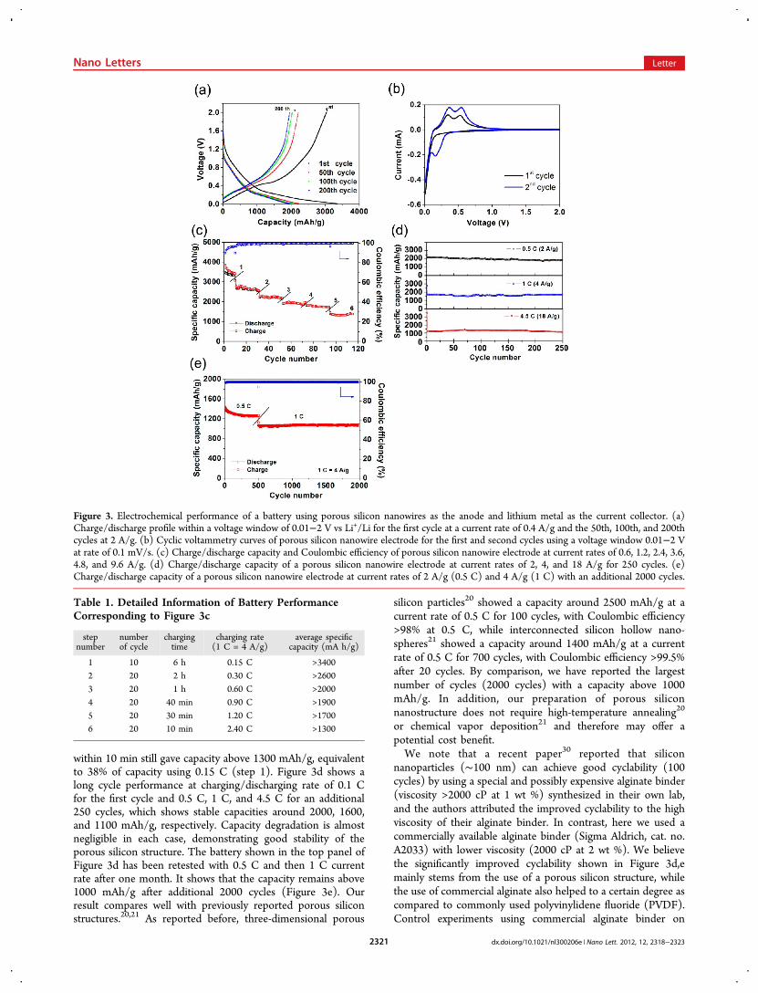
nanowires, several batteries after 10 cycles running at 0.1 C(0.4 A/g) were disassembled, and silicon anodes were washedwith acetonitrile and 0.5 M HNO3 to remove the SEI layer andthen dissolved in ethanol to make samples for TEMobservation. For clear comparison, Figure 4 shows the TEM
image of a porous Si nanowire before (Figure 4a) and aftercycling (Figure 4b,c). Figure 4b clearly shows that the nanowireremains highly porous, and the pore size does not changesignificantly after cycling (compared to Figure 4a). This agreeswell with theoretical analysis showing that porous silicon with alarge initial pore size and high porosity would not change itsstructure significantly after lithiation. Here the initial porediameter was around 8 nm, and the wall between adjacentpores had a thickness of about 6 nm (Figure 4a); after cycling,the pore diameter and the wall thickness are still around 7−8nm. The porous silicon nanowires are mostly amorphous(Figure 4c), with some dark dots less than 5 nm embedded inthe amorphous matrix. SAED in Figure 4d confirms that thedots are crystalline silicon. Similar observation of small portionof unlithiated silicon was reported before,17,20 and theunderlying mechanism is not fully understood and deservesfurther investigation. This provides evidence that lithiation anddelithiation in silicon is not homogeneous, therefore con-tributing to nonuniform stress distribution even at lowcharging/discharging rates. In some locations, accumulatedstress may be large enough to break silicon into fragments. Thisis especially true for nonporous structures, like siliconnanowires, which are not able to sustain its capacity afterlong cycling, since lithium ions can only intercalate into siliconfrom the very outer surface and generate a large concentrationgradient from surface to inner core, thus inducing large stress.In addition, low diffusivity of lithium ions in silicon generates alithium ion concentration gradient that also compromises thecapacity, as discussed with the simulation in Figure 1: the largerthe concentration gradient, the lower the charge/dischargecapacity. For porous silicon nanowires, the electrolyte goes
everywhere in the pores, and lithium intercalation happensinstantaneously wherever there is a contact between silicon andelectrolyte. Previous study shows that CVD grown siliconnanowire can also become porous after lithiation anddelithiation;31 however, there is still capacity degradation aftersome cycles for CVD silicon nanowires.11 As our simulation inFigure 1d shows, the stress in porous silicon after lithiationstrongly depends on the porosity, which is understandable. Wesuspect that when CVD grown silicon nanowires becomeporous after several cycles, the resulting porosity and locationof pores (surface of nanowires vs bulk of nanowires) can bedifferent from ours, which might lead to the observed differencein the cycling performance. Here, we also believe that borondoping increases electron conductivity in silicon, which mighthelp to reach a high capacity at high current rates, and thealginate, due to its high viscosity, could further improve thestructural stability during cycling. Further experiments arecurrently under way to produce and test porous siliconnanowires with different pore sizes and porosities.In conclusion, we have carried out both theoretical and
experimental studies on using porous doped silicon nanowiresfor lithium ion battery applications. Our simulation showsporous silicon having a large pore size and high porosity canmaintain its structure after lithium ion intercalation whilehaving low stress, which is beneficial for getting high capacityand long cycle retention. Porous silicon nanowires wereproduced by direct etching of boron-doped silicon wafers andexhibited superior electrochemical performance and long cyclelife as the anode material in lithium ion battery with alginateused as binder. The capacity remained stable above 2000, 1600,and 1100 mAh/g at current rates of 2, 4, and 18 A/g,respectively, even after 250 cycles. We believe the goodcyclability mainly stems from the use of a porous siliconstructure, while the use of a commercial alginate binder alsohelped to a certain degree as compared to commonly usedpolyvinylidene fluoride (PVDF). Our work demonstrates thegreat potential of porous silicon structures for energy storageapplications.
■ ASSOCIATED CONTENT
*S Supporting InformationAdditional information for methods used in simulation andfabrication of porous silicon nanowire anode. Controlexperimental results of using alginate binder on siliconnanoparticles and PVDF binder on porous silicon nanowires.This material is available free of charge via the Internet athttp://pubs.acs.org.
■ AUTHOR INFORMATION
Corresponding Author*[email protected]
Author Contributions§These authors contributed equally.
NotesThe authors declare no competing financial interest.
■ ACKNOWLEDGMENTS
We acknowledge the University of Southern California forfinancial support.
Figure 4. TEM images of silicon nanowires before (a) and after (b)lithiation after 10 cycles at a current rate of 0.4 A/g. (c) Enlarged TEMimage of (b) showing the amorphous silicon structure. (d) SAEDpattern showing black spots in (b) are crystalline silicon.
Nano Letters Letter
dx.doi.org/10.1021/nl300206e | Nano Lett. 2012, 12, 2318−23232322
■ REFERENCES(1) Li, H.; Wang, Z. X.; Chen, L. Q.; Huang, X. J. Adv. Mater. 2009,21 (45), 4593−4607.(2) Arico, A. S.; Bruce, P.; Scrosati, B.; Tarascon, J. M.; VanSchalkwijk, W. Nat. Mater. 2005, 4 (5), 366−377.(3) Choi, N. S.; Yao, Y.; Cui, Y.; Cho, J. J. Mater. Chem. 2011, 21(27), 9825−9840.(4) Kasavajjula, U.; Wang, C. S.; Appleby, A. J. J. Power Sources 2007,163 (2), 1003−1039.(5) Tarascon, J. M.; Armand, M. Nature 2001, 414 (6861), 359−367.(6) Scrosati, B. Nature 1995, 373 (6515), 557−558.(7) Nikolaev, V. P.; Morachevskii, A. G.; Demidov, A. I.; Bairachnyi,E. V. Russ. J. Appl. Chem. 1980, 53 (9), 1549−1551.(8) Boukamp, B. A.; Lesh, G. C.; Huggins, R. A. J. Electrochem. Soc.1981, 128 (4), 725−729.(9) Takamura, T.; Ohara, S.; Uehara, M.; Suzuki, J.; Sekine, K. J.Power Sources 2004, 129 (1), 96−100.(10) Yin, J. T.; Wada, M.; Yamamoto, K.; Kitano, Y.; Tanase, S.;Sakai, T. J. Electrochem. Soc. 2006, 153 (3), A472−A477.(11) Chan, C. K.; Peng, H. L.; Liu, G.; McIlwrath, K.; Zhang, X. F.;Huggins, R. A.; Cui, Y. Nat. Nanotechnol. 2008, 3 (1), 31−35.(12) Peng, K. Q.; Jie, J. S.; Zhang, W. J.; Lee, S. T. Appl. Phys. Lett.2008, 93 (3), 033105−033107.(13) Cui, L.-F.; Yang, Y.; Hsu, C.-M.; Cui, Y. Nano Lett. 2009, 9 (9),3370−3374.(14) Liu, X. H.; Zhang, L. Q.; Zhong, L.; Liu, Y.; Zheng, H.; Wang, J.W.; Cho, J.-H.; Dayeh, S. A.; Picraux, S. T.; Sullivan, J. P.; Mao, S. X.;Ye, Z. Z.; Huang, J. Y. Nano Lett. 2011, 11 (6), 2251−2258.(15) Dimov, N.; Kugino, S.; Yoshio, M. Electrochim. Acta 2003, 48(11), 1579−1587.(16) Kim, H.; Seo, M.; Park, M.-H.; Cho, J. Angew. Chem., Int. Ed.2010, 49 (12), 2146−2149.(17) Park, M. H.; Kim, M. G.; Joo, J.; Kim, K.; Kim, J.; Ahn, S.; Cui,Y.; Cho, J. Nano Lett. 2009, 9 (11), 3844−3847.(18) Song, T.; Xia, J.; Lee, J.-H.; Lee, D. H.; Kwon, M.-S.; Choi, J.-M.; Wu, J.; Doo, S. K.; Chang, H.; Il Park, W.; Zang, D. S.; Kim, H.;Huang, Y.; Hwang, K.-C.; Rogers, J. A.; Paik, U. Nano Lett. 2010, 10(5), 1710−1716.(19) Zhou, S.; Wang, D. W. ACS Nano 2010, 4 (11), 7014−7020.(20) Kim, H.; Han, B.; Choo, J.; Cho, J. Angew. Chem., Int. Ed. 2008,47 (52), 10151−10154.(21) Yao, Y.; McDowell, M. T.; Ryu, I.; Wu, H.; Liu, N.; Hu, L.; Nix,W. D.; Cui, Y. Nano Lett. 2011, 11 (7), 2949−2954.(22) Wang, X. L.; Han, W. Q. ACS Appl. Mater. Inter. 2010, 2 (12),3709−3713.(23) Sun, C. Y.; Qin, C.; Wang, C. G.; Su, Z. M.; Wang, S.; Wang, X.L.; Yang, G. S.; Shao, K. Z.; Lan, Y. Q.; Wang, E. B. Adv. Mater. 2011,23, (47), 5629.(24) Obrovac, M. N.; Christensen, L. Electrochem. Solid-State Lett.2004, 7 (5), A93−A96.(25) Zhang, X.; Shyy, W.; Sastry, A. M. J. Electrochem. Soc. 2007, 154(10), A910−A916.(26) Park, J.; Lu, W.; Sastry, A. M. J. Electrochem. Soc. 2011, 158 (2),A201−A206.(27) Qu, Y.; Zhou, H.; Duan, X. Nanoscale 2011, 3 (10), 4060−4068.(28) Hochbaum, A. I.; Gargas, D.; Hwang, Y. J.; Yang, P. Nano Lett.2009, 9 (10), 3550−3554.(29) Li, J.; Dahn, J. R. J. Electrochem. Soc. 2007, 154 (3), A156−A161.(30) Kovalenko, I.; Zdyrko, B.; Magasinski, A.; Hertzberg, B.;Milicev, Z.; Burtovyy, R.; Luzinov, I.; Yushin, G. Science 2011, 333(6052), 75−79.(31) Choi, J. W.; McDonough, J.; Jeong, S.; Yoo, J. S.; Chan, C. K.;Cui, Y. Nano Lett. 2010, 10, 1409−1413.
Nano Letters Letter
dx.doi.org/10.1021/nl300206e | Nano Lett. 2012, 12, 2318−23232323