Magnetotransport in Co-Doped ZnO Nanowires · Received December 18, 2008; Revised Manuscript...
6
Subscriber access provided by - Access paid by the | UC Berkeley Library Nano Letters is published by the American Chemical Society. 1155 Sixteenth Street N.W., Washington, DC 20036 Letter Magnetotransport in Co-Doped ZnO Nanowires Wenjie Liang, Benjamin D. Yuhas, and Peidong Yang Nano Lett., 2009, 9 (2), 892-896• DOI: 10.1021/nl8038184 • Publication Date (Web): 26 January 2009 Downloaded from http://pubs.acs.org on March 13, 2009 More About This Article Additional resources and features associated with this article are available within the HTML version: • Supporting Information • Access to high resolution figures • Links to articles and content related to this article • Copyright permission to reproduce figures and/or text from this article
Transcript of Magnetotransport in Co-Doped ZnO Nanowires · Received December 18, 2008; Revised Manuscript...
Subscriber access provided by - Access paid by the | UC Berkeley Library
Nano Letters is published by the American Chemical Society. 1155 SixteenthStreet N.W., Washington, DC 20036
Letter
Magnetotransport in Co-Doped ZnO NanowiresWenjie Liang, Benjamin D. Yuhas, and Peidong Yang
Nano Lett., 2009, 9 (2), 892-896• DOI: 10.1021/nl8038184 • Publication Date (Web): 26 January 2009
Downloaded from http://pubs.acs.org on March 13, 2009
More About This Article
Additional resources and features associated with this article are available within the HTML version:
• Supporting Information• Access to high resolution figures• Links to articles and content related to this article• Copyright permission to reproduce figures and/or text from this article
Magnetotransport in Co-Doped ZnONanowiresWenjie Liang, Benjamin D. Yuhas, and Peidong Yang*
Department of Chemistry, UniVersity of California, Berkeley, California 94720
Received December 18, 2008; Revised Manuscript Received January 14, 2009
ABSTRACT
Electrical and magnetotransport measurements were performed on individual Co-doped ZnO dilute magnetic semiconductor nanowires. Theelectron transport studies show that the electron mobility could be as high as 75 cm2/(V·s), and we observed positive magnetoresistivity (MR)at low magnetic field and negative MR at higher magnetic field. s-d exchange-induced spin splitting of the conduction band could accountfor positive MR while suppression of weak localization of impurity centers could account for the negative MR. Lowering the carrier concentrationin these nanowires through the application of a gate voltage tends to induce a larger magnitude MR as well as additional fine structure in theMR curves.
Spintronics has emerged as a promising field for futuresemiconductor devices.1,2 The ability to manipulate boththe spin and charge degrees of freedom is necessary to realizeadvanced functionality in these devices. Recently, dilutemagnetic semiconducting (DMS) materials have generatedextraordinary research interest due to their potential as idealmaterials for spintronic devices. In DMS materials, thecollective magnetic ordering has been shown theoretically3
and experimentally4,5 to be mediated by the semiconductorcharge carriers, as well as electron scattering at localizedmagnetic impurities and electron-electron interactions. Theferromagnetic ordering in these systems could then lead tospin-polarized charge transport.6-8 Electrostatic control ofmagnetization has been demonstrated in Mn-doped InAs andGaAs thin films;9 however, the Curie temperature (TC) ofthese materials remains far below room temperature. Forpractical applications, TC must be above 300 K. Transitionmetal (TM) doped wide band gap semiconductors, such asZnO or GaN, are theoretically predicted to have TC above300 K,3 so they could be potential material candidates forpractical spintronic devices. In the past, room temperatureferromagnetism has been experimentally demonstrated in Co-or Mn-doped ZnO10 thin films, although the origin of theobserved magnetic properties in TM-doped ZnO materialsis still quite controversial11 and further investigation of chargeand spin transport through these materials is needed. Inaddition, the majority of magnetotransport studies on DMSmaterials have been in either the bulk or thin film forms.There are far fewer reports of spin transport in lower-dimensional DMS materials, such as nanowires.
In this Letter, we report electron transport and magne-toresistance studies of Co-doped ZnO nanowires. Pure andTM-doped ZnO nanowires were synthesized with a solution
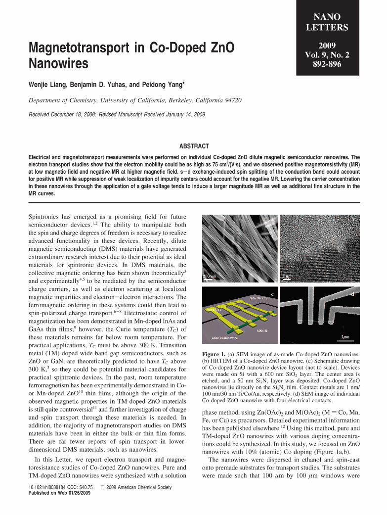
phase method, using Zn(OAc)2 and M(OAc)2 (M ) Co, Mn,Fe, or Cu) as precursors. Detailed experimental informationhas been published elsewhere.12 Using this method, pure andTM-doped ZnO nanowires with various doping concentra-tions could be synthesized. In this study, we focused on ZnOnanowires with 10% (atomic) Co doping (Figure 1a,b).
The nanowires were dispersed in ethanol and spin-castonto premade substrates for transport studies. The substrateswere made such that 100 µm by 100 µm windows were
Figure 1. (a) SEM image of as-made Co-doped ZnO nanowires.(b) HRTEM of a Co-doped ZnO nanowire. (c) Schematic drawingof Co-doped ZnO nanowire device layout (not to scale). Deviceswere made on Si with a 600 nm SiO2 layer. The center area isetched, and a 50 nm SixNy layer was deposited. Co-doped ZnOnanowires lie directly on the SixNy film. Contact metals are 1 nm/100 nm/30 nm Ti/Co/Au, respectively. (d) SEM image of individualCo-doped ZnO nanowire with four electrical contacts.
NANOLETTERS
2009Vol. 9, No. 2
892-896
10.1021/nl8038184 CCC: $40.75 2009 American Chemical SocietyPublished on Web 01/26/2009

opened on a 600 nm thick SiO2 covered Si chip. Then, 50nm of SixNy was grown on the surface so that the depositedZnO nanowires would lie directly on the Si surface with only50 nm SixNy as spacer (Figure 1c,d). The substrates wereprepared with alignment markers so standard e-beam lithog-raphy could be performed to define electrical contacts toindividual nanowires. 1 nm/100 nm/20 nm Ti/Co/Au weredeposited as electrode materials in an e-beam evaporator afterthe nanowire surface was cleaned in an O2 plasma cleanerfor 30 s at a power of 50 W.
Room temperature electron transport measurements wereperformed in a Faraday cage with a multifunctional DACcard (National Instrument 6052E) as voltage sources andsignal collecting unit. Low-temperature and magnetotransportmeasurements were performed in a superconducting quantuminterference device (SQUID) and a cryostat with a split coilsuperconducting magnet so that the sample could be rotatedwith respect to the magnetic field direction. A Keithley(model 236) source-measurement unit, a Stanford ResearchSystem lock-in amplifier (SR810), and a Digital Instrument
current preamplifer (DL-1211) were used for the low-temperature measurements.
Panels a and b of Figure 1 show scanning electronmicroscopy (SEM) and high-resolution transmission micros-copy (HRTEM) images of representative Co-doped ZnOnanowires we used for our studies. As-made Co-doped ZnOnanowires have a diameter of 35 ( 5 nm and length up to5 µm. HRTEM image (Figure 1b) shows that these Co-dopedZnO nanowires are single crystalline. Further careful ex-amination confirmed that these nanowires possess a uniformdoping profile with no detectable secondary phases or dopantconcentration gradients.13 This makes our Co-doped ZnOnanowires an ideal candidate for magnetotransport studiesin TM-doped ZnO materials. Collective magnetizationmeasurements, presented previously,13 indicate that thenanowires have a weak ferromagnetism that persists up toroom temperature, with a paramagnetic component dominat-ing at low temperature.
For our magnetotransport studies, we made two-probecurrent (I)-voltage (V) measurements and four-probe (Figure1, panels c and d) I-V measurements on individual 10%Co-doped ZnO nanowires. The majority of our devices showlinear I-V curves with two-probe and four-probe resistancesthat differ by less than 1%, which suggests that we haveOhmic contact to the nanowires and that contact resistance
Figure 2. Electron transport measurement of a single Co-dopedZnO nanowire. (a) I-V curves taken at different gate voltages, Vg.The most conductive I-V curve was from Vg ) 10. Each curvebelow is taken at different gate voltage with 0.5 V interval. Inset:Conductance vs Vg plot for the same device. (b) Temperature-dependent resistance of the device.
Figure 3. Magnetoresistance measurement at (a) different temper-atures and (b) different field orientations taken at 2.5 K and 29 Vgate voltage.
Nano Lett., Vol. 9, No. 2, 2009 893
is negligible. Figure 2a shows two-probe I-V curves takenwith different applied gate voltages, Vg (-10 to 10 V witha step size of 0.5 V). The conductance, G, increases withincreasing gate voltage, indicating n-type conduction. Theinset shows the nanowire conductance versus Vg. The deviceis turned on when positive gate voltage is applied and theconductance increases with Vg. The electron mobility iscalculated from the transconductance, dG/dVg, and from thegeometry of the nanowire.14 We estimate the electronmobility in our Co-doped ZnO nanowires to be on the orderof tens of cm2/(V·s), with the highest value to be 75 cm2/
(V·s). This number is comparable to the best-reportedmobilities of n-type ZnO materials. The carrier concentrationis on the order of (2-5) × 1018 cm-3. This suggests that theCo dopants do not drastically decrease the mobility due totheir similar ionic radii. In a previous publication,13 wereported that our doping process occurs with a high degreeof order retained in the nanowires; there are no widespreaddefects or dislocations in the ZnO lattice as a result of TMdopant incorporation. This high degree of order gave rise toa relatively weak ferromagnetic coupling, as predicted bytheory.14,15 We thus see that our ordered doping process,
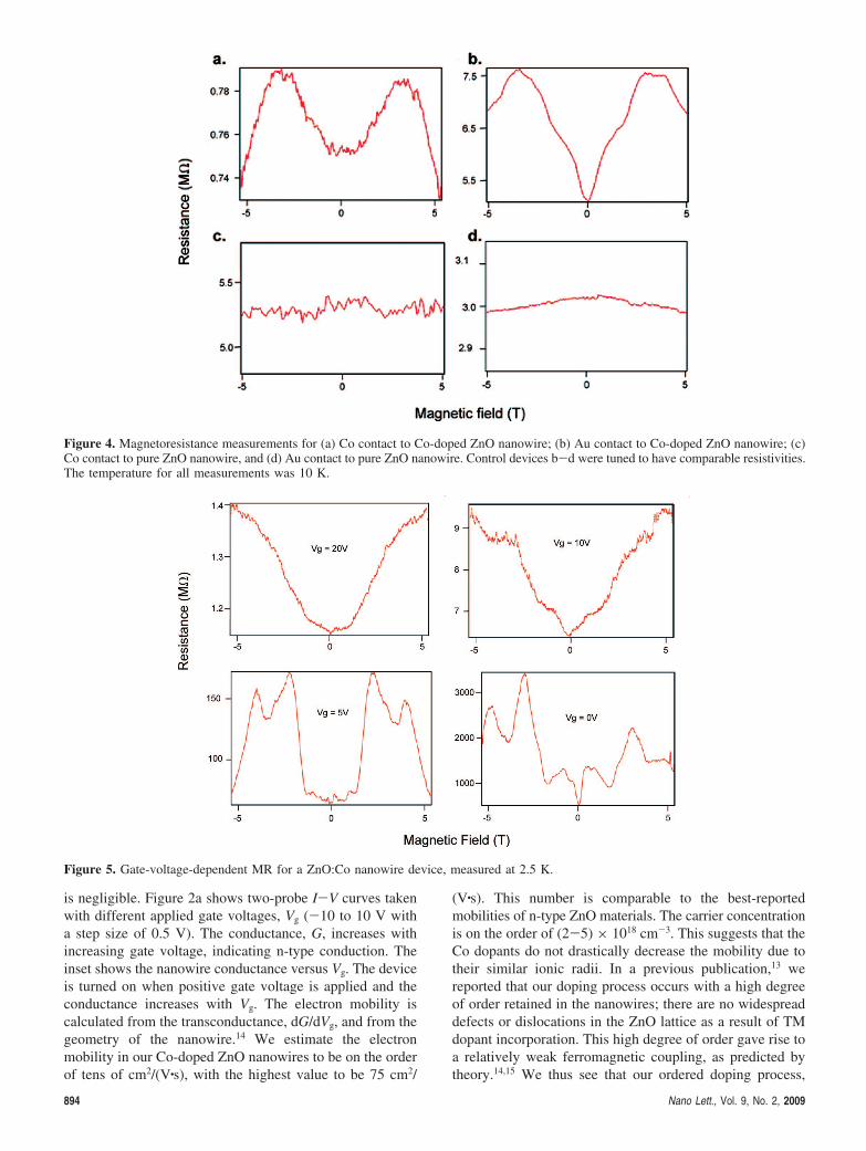
Figure 4. Magnetoresistance measurements for (a) Co contact to Co-doped ZnO nanowire; (b) Au contact to Co-doped ZnO nanowire; (c)Co contact to pure ZnO nanowire, and (d) Au contact to pure ZnO nanowire. Control devices b-d were tuned to have comparable resistivities.The temperature for all measurements was 10 K.
Figure 5. Gate-voltage-dependent MR for a ZnO:Co nanowire device, measured at 2.5 K.
894 Nano Lett., Vol. 9, No. 2, 2009
although yielding weaker ferromagnetism, endows ournanowires with well-defined intrinsic transport properties andthat both the observed electronic and magnetic behavior canbe explained by a common mechanism.
The resistance of the nanowires was measured at temper-ature between 5 and 300 K. The temperature-dependentresistance plot (Figure 2b) shows the resistance of a singlenanowire plotted in a logarithmic scale as a function ofreciprocal temperature 1/T. In the simplest modeling, log Rcan be written as
log R)Ea ⁄ kbT+ constant
where Ea is the activation energy that electrons need toovercome to hop into the conduction band of the ZnOnanowires and kB is the Boltzmann constant. Fitting our dataof doped ZnO nanowires, we found that Ea varies from 38to 45 meV.
Figure 3 represents one of our typical magnetotransportmeasurements. In Figure 3a, magnetoresistance (MR) wasrecorded as a function of magnetic field (B) at differenttemperatures. The axial direction of the nanowire was alignedwith the magnetic field. After the nanowire was slowlycooled down to 2.5 K, resistance was monitored using a lock-in amplifier while magnetic field was swept between -5 and5 T. Interestingly, the measured MR as a function ofmagnetic field is not monotonic. Positive MR was observedwith small B, and when B is further increased, a maximumMR was reached. A further increase in B results in decreasingMR. Negative MR could be observed at high values of B.The measured maximum positive MR (Rmax) is 5%, occurringat a turnover field of 3.3 T. At 5 T, MR drops by 5%compared to Rmax. This phenomenon of MR reversal wasrepeatedly observed in all other Co-doped ZnO nanowireswe tested, although the turnover field where the maximumMR was observed differs slightly from sample to sample.In some cases, we only observed a shoulder up to 5 T. Thehighest MR achieved was 24%. The temperature dependenceof the MR was also presented in Figure 3a. The magnitudeof the MR decreases as the temperature increases, withnoticeable MR vanishing above 40 K.
Figure 3b shows MR plots at 2.5 K as a function ofmagnetic field orientation relative to the c axis of thenanowire. When the field direction changed from parallel toc axis to perpendicular to it, the general observed MR versusfield curve shape remains the same, but the turnover fielddecreases from 3.3 to 2.1 T, and a greater negative MR wasobserved at high field (∼20% compared with Rmax). Thereduction of turnover field upon sample rotation, as well asthe larger negative MR at high field, was observed in multipledevices. These observations suggest that perpendicular fieldfavors negative MR. One plausible reason might be that thehard axial direction for magnetizations is along the nanowiredirection; this has been shown in numerous EPR and bulkmagnetization measurements.16 No significant MR hysteresiswas observed when the field sweeping direction was changed.
To confirm that the observed MR indeed arises from Codoping in the ZnO lattice, additional nanowire devices weretested: (1) Au-contacted Co-doped ZnO nanowires, (2) Co-contacted pure ZnO nanowires, and (3) Au-contacted pure
ZnO nanowires. The changing of MR from positive tonegative direction was also observed in Au-contacted Co-doped ZnO nanowires, but it is clearly absent in MR plotsof both Co-contacted pure ZnO nanowires and Au-contactedpure ZnO nanowires (Figure 4). Interestingly, we note thatour Au-contacted pure ZnO nanowires showed a smallnegative MR, the origin of which is still unclear at this point.Nevertheless, the above control experiments show that ourobserved MR behaviors in our Co-doped ZnO nanowires areintrinsic properties to the doped nanowires themselves.
In n-type ZnO, the conduction band is primarily comprisedof s electrons. The introduction of a transition metal impuritycan induce a spin-split conduction band due to s-d exchangeinteraction. Electron redistribution between the two subbandsin the presence of a magnetic field leads to positive MR dueto relaxation time changes for electrons at the Fermisurfaces.15 The electron spin-disorder scattering is alsofavorable for a low-temperature/low field positive MR.6,17
When the temperature is raised, the Fermi energy becomesmuch larger than the energy difference between the subbands,so the difference of the electron populations in the twosubbands would be negligible.18-20 Thus, the positive MRbecomes weaker as temperature increases. At higher mag-netic fields, the negative MR observed could be attributedto the suppression of weak localization of impurity centers.In higher magnetic fields, the alignment of the Co magneticmoment and more polarized spin current lead to non-negligible reduction of electron scattering and hence resis-tance, contributing to the turnover of the MR curves.18 Theobservation of positive and negative MR in our Co-dopedZnO nanowire device is the result of the competition betweenthese two physical processes. Similar behavior was alsopreviously observed in pulse laser deposition (PLD) preparedCo-doped thin films.6,20-22
Since the carrier concentration of the host semiconductorcan greatly influence DMS material magnetic properties, itis interesting to study the MR of the same nanowire atdifferent carrier concentrations. The carrier concentration cansimply be tuned by the application of a gate voltage. Figure5 shows the MR of a Co-doped ZnO nanowire while itsconductance was tuned by back gating. In general, themagnitude of the MR increases when the conductionelectrons are slowly depleted, i.e., as gate voltage decreases.The positive MR magnitude increased from 20% to 48% to120% to 300% while the gate voltage was lowered from 20V to 10 V to 5 V to 0 V. The increase of positive MR couldbe a result of more spin-polarized current at lower conductionelectron concentrations. As temperature was increased, MRpersists at higher temperature when gate voltage was tunedmore negatively. Curiously, at lower gate voltages, the MRcurve shapes become much more complex, with shouldersand multiple peaks as the applied field was modulated. Thesesubtle features could be related to fine details in the bandstructure and additional spin scattering processes at theimpurity centers, although further research is necessary toconfirm this hypothesis. Similar MR behavior was previouslyobserved in Co-doped ZnO thin films,20 and we believe that
Nano Lett., Vol. 9, No. 2, 2009 895
this is the first report of such anomalous MR in Co-dopedZnO nanowires.
To summarize, electrical and magnetotransport measure-ments were performed on individual Co-doped ZnO nano-wires. The electron transport studies show that the electronmobility could be as high as 75 cm2/(V·s), and we observedpositive MR at low magnetic field and negative MR at highermagnetic field. s-d exchange-induced spin splitting of theconduction band could account for positive MR whilesuppression of weak localization of impurity centers couldaccount for the negative MR. Lowering the carrier concen-tration in these NWs through the application of a gate voltagetends to induce a larger magnitude MR as well as additionalfine structure in the MR curves. Our results represent thefirst magnetotransport experiments for high-quality Co-dopedZnO nanowires, and through these and future efforts, we seekto attain a better understanding of the mechanism of magneticordering in DMS nanowires that will ultimately lead to theconstruction of practical spintronic devices.
Acknowledgment. We thank WIN for funding supportand Professor Frances Hellman for the use of their SQUID.We thank Dr. Rong Fan for SiNx substrate preparation. Wethank Dr. Ajey Jacob and Dmitri Nikonov for thoughtfuldiscussion.
References(1) Wolf, S. A.; Awschalom, D. D.; Buhrman, R. A.; Daughton, J. M.;
von Molnar, S.; Roukes, M. L.; Chitchelkanova, A. Y.; Treger, D. M.Science 2001, 294, 1488.
(2) Awschalon, D. D.; Flatte, M. E. Nat. Phys. 2007, 2, 153.
(3) Ditel, T.; Ohno, H.; Matsukura, F.; Clbert, J.; Ferrand, D. Science2000, 287, 1019.
(4) Ohno, Y.; Young, D. K.; Beschoten, B.; Matsukura, F.; Ohno, H.;Awschalom, D. D. Nature 1999, 402, 790.
(5) Tanaka, M.; Higo, Y. Phys. ReV. Lett. 2001, 87, 026602.(6) Xu, Q.; Hartmann, L.; Zhou, S.; Mcklich, A.; Helm, M.; Biehne, G.;
Hochmuth, H.; Lorenz, M.; Grundmann, M.; Schmidt, H. Phys. ReV.Lett. 2008, 101, 076601.
(7) Ruster, C.; Borzenko, T.; Gould, C.; Schmidt, G.; Molenkamp, L. W.;Liu, X.; Wojtowicz, T. J.; Furdyna, J. K.; Yu, Z. G.; Flatte, M. E.Phys. ReV. Lett. 2003, 91, 216602.
(8) Choi, H.; et al. AdV. Mater. 2005, 17, 1348.(9) Ohno, H.; Chiba, D.; Matsukura, F.; Omiya, T.; Abe, E.; Dietl, T.;
Ohno, Y.; Ohtani, K. Nature 2000, 408, 944.(10) Bouloudenine, M.; Viart, N.; Colis, S.; Kortus, J.; Dinia, A. Appl.
Phys. Lett. 2005, 87, 052501.(11) Coey, J. M. D.; Chambers, S. A. MRS Bull. 2008, 33, 1053.(12) Yuhas, B.; Zitoun, D. O.; Pauzauskie, P. J.; He, R.; Yang, P. Angew.
Chem., Int. Ed. 2006, 45, 420.(13) Yuhas, B.; Fakra, S.; Marcus, M. A.; Yang, P. Nano Lett. 2007, 7,
905.(14) Berciu, M.; Bhatt, R. N. Phys. ReV. Lett. 2001, 87, 107203.(15) Coey, J. M. D.; Venkatesan, M.; Fitzgerald, C. B. Nat. Mater. 2005,
4, 173.(16) Venkatesan, M.; Fitzgerald, C. B.; Lunney, J. G.; Coey, J. M. D. Phys.
ReV. Lett. 2004, 93, 177206.(17) Shapira, Y.; Kautz, R. L. Phys. ReV. B 1974, 10, 4781.(18) Lee, P. A.; Ramakrishnan, T. V. ReV. Mod. Phys. 1985, 57, 287.(19) Budhani, R. C.; Pant, P.; Rakshit, R. K.; Senapati, K.; Mandal, S.;
Pandey, N. K.; Kumar, J. J. Phys.: Condens. Matter 2005, 17, 75.(20) Xu, Q.; Hartmann, L.; Schmidt, H.; Hochmuth, H.; Lorenz, M.;
Schmidt-Grund, R.; Sturm, C.; Spemann, D.; Grundmann, M. Phys.ReV. B 2006, 73, 205342.
(21) Xu, Q.; et al. Thin Solid Films 2006, 515, 2549.(22) Dietl, T.; Andrearczyk, T.; Lipinska, A.; Kiecana, M.; Tay, M.; Wu,
Y. Phys. ReV. B 2007, 76, 155312.
NL8038184
896 Nano Lett., Vol. 9, No. 2, 2009