1 Introduction to Microcontroller Microcontroller Fundamentals & Programming.
Pira.cz P232 Microcontroller
FM Broadcast Radio Data System Encoder MCU
with two communication ports
DESCRIPTION
The P232 Microcontroller forms a fully digital Radio Data System encoder that has been developed especially for FM broadcasting. It implements physical and data-link layers and supports extended set of RDS services. The device provides two independent hardware serial communication ports and supports optional I2C slave peripherals such as EEPROM memory,
RTC or digital potentiometer.
FEATURES
Single supply 3.0 to 5.5 V Typical operating current: 12 mA @ 5.0 V Minimum external parts I
2C bus for external peripherals like EEPROM,
real time clock or digital potentiometer External TA and Program switch Two indication LED outputs Integrated support for HD44780 based LCD Industrial temperature range Clocked with low-cost 16 MHz crystal Both stereo and mono operation possible Fully integrated DSP pilot tone filter and PLL Parallel 8-bit D/A converter, 592 kHz sampling
rate (over-sampled) Only simple output filter required RDS/RBDS signal:
conforms to CENELEC EN 50067 / EN 62106 2 independent hardware serial communication
ports for RDS control and configuration Backward compatible with PIRA32 Firmware update capability Final product requires no factory adjustment RoHS compliant Packages available: 40-lead PDIP
44-lead TQFP
APPLICATIONS
FM broadcast RDS encoders with up to two
independent physical communication ports
Important Note:
This datasheet is not intended to be a complete P232 system designer’s reference source. For more information on the features, characteristics, control and use refer to these documents: “P232 RDS Encoder Technical Manual” (available online) “P232/PIRA32 Device Configuration” (available on request)
The manufacturer is not liable for any damages, including but not limited to, lost profits, lost savings, or other incidental or consequential damages arising out of the use of this product. No part of this datasheet may be reproduced or transmitted in any form or by any means, electronic or mechanical, including photocopying, recording or information storage and retrieval systems, for any purpose other than the purchaser's personal use. Information in this document is subject to change without notice.
Revision 2019-03-12

P232 Microcontroller
m232.pdf – page 2 © 2019 Pira.cz
TABLE OF CONTENTS
1 Pin Diagrams and Description ...................................................................................................................... 3 1.1 40-Pin PDIP ........................................................................................................................................... 3 1.2 44-Pin TQFP .......................................................................................................................................... 3 1.3 Pin descriptions ...................................................................................................................................... 4 1.4 Internal logical structure (simplified) ....................................................................................................... 6
2 Electrical Characteristics ............................................................................................................................... 7
3 External Devices Supported .......................................................................................................................... 8 3.1 External I
2C devices supported .............................................................................................................. 8
3.2 Support for external LCD display ........................................................................................................... 8
4 Connection Diagrams and Application Notes .............................................................................................. 9 4.1 Basic connection diagram ...................................................................................................................... 9 4.2 Design notes .........................................................................................................................................10
4.2.1 Power supply ......................................................................................................................................10 4.2.2 Hardware reset ...................................................................................................................................10 4.2.3 Crystal oscillator .................................................................................................................................10 4.2.4 MPX/Pilot input and pilot PLL .............................................................................................................10 4.2.5 RS-232 interface (Port 1, Port 2) ........................................................................................................11 4.2.6 Digital-to-Analog converter .................................................................................................................11 4.2.7 Output low-pass filter ..........................................................................................................................12
4.3 Typical applications (simplified block diagrams) ...................................................................................13 4.3.1 RDS Encoder with RS-232 and USB interface ...................................................................................13 4.3.2 RDS Encoder with RS-232 interface and independent control from embedded microcomputer .........13
4.4 Sample application circuits ....................................................................................................................14 4.4.1 Real time backup sample circuit .........................................................................................................14 4.4.2 Onboard Serial to USB adapter sample circuit ...................................................................................14 4.4.3 RDS level control circuit ......................................................................................................................15 4.4.4 Analog section sample circuit .............................................................................................................15 4.4.5 Part list ................................................................................................................................................16
5 Package Details .............................................................................................................................................17 5.1 40-Lead Plastic Dual In-Line (PDIP) 600 mil Body ................................................................................17 5.2 44-Lead Plastic Thin Quad Flatpack (TQFP) – 10x10x1 mm Body .......................................................18
P232 Microcontroller
© 2019 Pira.cz m232.pdf – page 3
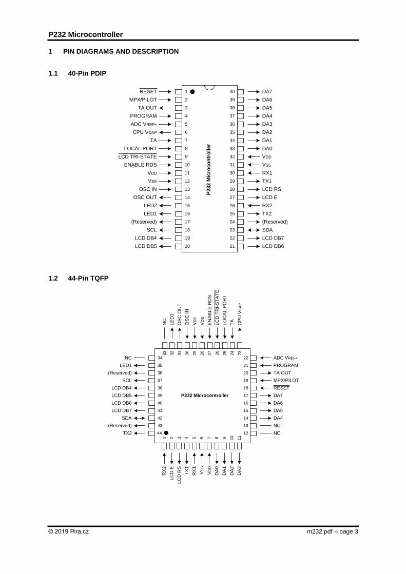
1 PIN DIAGRAMS AND DESCRIPTION
1.1 40-Pin PDIP
1.2 44-Pin TQFP
1
P2
32 M
icro
co
ntr
oll
er
2
3
4
5
6
7
8
9
10
35
34
33
32
31
40
39
38
37
36
PROGRAM
ADC VREF+
CPU VCAP
TA
LOCAL PORT
DA5
DA4
DA3
DA2
DA1
DA6
DA7
DA0
VDD
VSS
LCD TRI-STATE
ENABLE RDS
TA OUT
MPX/PILOT
RESET
OSC OUT
LED2
LED1
(Reserved)
SCL
LCD DB4
LCD DB5
OSC IN
VSS
VDD 11
12
13
14
15
16
17
18
19
20
LCD RS
LCD E
RX2
TX2
(Reserved)
TX1
RX1
SDA
LCD DB7
LCD DB6
25
24
23
22
21
30
29
28
27
26
NC
LED1
34
35
(Reserved)
SCL
36
37
LCD DB4
LCD DB5
38
39
LCD DB6
LCD DB7
40
41
SDA
(Reserved)
42
43
TX2 44
RX
2
LC
D E
2
LC
D R
S
TX
1
3 4
RX
1
VS
S
5 6
VD
D
DA
0
7 8
DA
1
DA
2
9 10
DA
311
22 ADC VREF+
MPX/PILOT
RESET
DA7
DA6
DA5
TA OUT
PROGRAM
DA4
NC
NC
16
15
14
13
12
21
20
19
18
17
33
NC
OS
C I
N
VS
S
VD
D
EN
AB
LE
RD
S
LC
D T
RI-
ST
AT
E
OS
C O
UT
LE
D2
LO
CA
L P
OR
T
TA
CP
U V
CA
P
27
26
25
24
23
32
31
30
29
28
1
P232 Microcontroller

P232 Microcontroller
m232.pdf – page 4 © 2019 Pira.cz
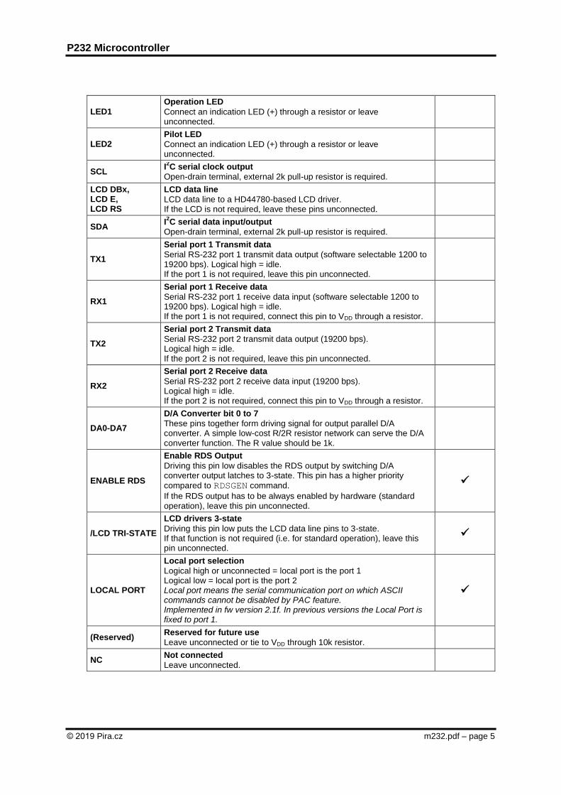
1.3 Pin descriptions
Pin name Description Internal
weak pull-up
/RESET
Device reset
Logical low on this pin holds the device in reset state. If the reset function is not required, connect this pin to VDD through 10k resistor.
MPX/PILOT
MPX or pilot tone analogue input for RDS sync.
MPX or pilot sample input for RDS sub-carrier synchronization in case of stereo transmission. Average DC component of the input signal should be (ADC VREF+ / 2). Peak value should not exceed VSS and ADC VREF+ boundaries. If the pilot sync. function is not required, connect this pin to VSS.
PROGRAM
Program select
Selects between two different RDS data sets (program 1 or program 2). If the program external switching function is not required, connect this pin to VDD through a resistor.
TA OUT TA output
RDS Traffic Announcement (TA) logical output from internal decoder. Can be left unconnected.
ADC VREF+
Positive voltage reference for internal A/D converter
Connect this pin to VDD through a 15Ω resistor. Decoupling this pin to VSS using a 10 μF capacitor is recommended. Direct connection of this pin to VDD is not recommended due to noise parameters. This pin must be connected also if the pilot sync. function is not required!
CPU VCAP
External filter capacitor connection
A low-ESR (< 5Ω) capacitor is required on this pin to stabilize internal voltage regulator output voltage. The capacitor must be connected to ground. The type can be ceramic or tantalum, a value of 10 μF.
TA
TA switch input
RDS Traffic Announcement (TA) flag control. If the TA external switching function is not required, connect this pin to VDD through a resistor.
VDD
Positive supply
Apply VDD power supply voltage to this pin. All VDD pins must be connected. Decoupling capacitor is required on every pair of VDD and VSS pins. A 100 nF 10-20V capacitor is recommended. Ceramic capacitors are recommended. The decoupling capacitors should be placed as close to the pins as possible. It is recommended to add a second ceramic type capacitor in parallel to the above described decoupling capacitor. The value of the second capacitor should be 1 nF.
VSS Ground reference
All VSS pins must be connected.
OSC IN Crystal oscillator input
Tie to 16 MHz crystal pin or an integrated crystal oscillator output.
OSC OUT
Crystal oscillator output
Tie to 16 MHz crystal pin. Leave unconnected if an integrated crystal oscillator is used for clocking the device via pin OSC IN. Can be used for clocking another device on the board.
P232 Microcontroller
© 2019 Pira.cz m232.pdf – page 5
LED1 Operation LED
Connect an indication LED (+) through a resistor or leave unconnected.
LED2 Pilot LED
Connect an indication LED (+) through a resistor or leave unconnected.
SCL I2C serial clock output
Open-drain terminal, external 2k pull-up resistor is required.
LCD DBx, LCD E, LCD RS
LCD data line
LCD data line to a HD44780-based LCD driver. If the LCD is not required, leave these pins unconnected.
SDA I2C serial data input/output
Open-drain terminal, external 2k pull-up resistor is required.
TX1
Serial port 1 Transmit data
Serial RS-232 port 1 transmit data output (software selectable 1200 to 19200 bps). Logical high = idle. If the port 1 is not required, leave this pin unconnected.
RX1
Serial port 1 Receive data
Serial RS-232 port 1 receive data input (software selectable 1200 to 19200 bps). Logical high = idle. If the port 1 is not required, connect this pin to VDD through a resistor.
TX2
Serial port 2 Transmit data
Serial RS-232 port 2 transmit data output (19200 bps). Logical high = idle. If the port 2 is not required, leave this pin unconnected.
RX2
Serial port 2 Receive data
Serial RS-232 port 2 receive data input (19200 bps). Logical high = idle. If the port 2 is not required, connect this pin to VDD through a resistor.
DA0-DA7
D/A Converter bit 0 to 7
These pins together form driving signal for output parallel D/A converter. A simple low-cost R/2R resistor network can serve the D/A converter function. The R value should be 1k.
ENABLE RDS
Enable RDS Output
Driving this pin low disables the RDS output by switching D/A converter output latches to 3-state. This pin has a higher priority
compared to RDSGEN command.
If the RDS output has to be always enabled by hardware (standard operation), leave this pin unconnected.
/LCD TRI-STATE
LCD drivers 3-state
Driving this pin low puts the LCD data line pins to 3-state. If that function is not required (i.e. for standard operation), leave this pin unconnected.
LOCAL PORT
Local port selection
Logical high or unconnected = local port is the port 1 Logical low = local port is the port 2 Local port means the serial communication port on which ASCII commands cannot be disabled by PAC feature. Implemented in fw version 2.1f. In previous versions the Local Port is fixed to port 1.
(Reserved) Reserved for future use
Leave unconnected or tie to VDD through 10k resistor.
NC Not connected
Leave unconnected.

P232 Microcontroller
m232.pdf – page 6 © 2019 Pira.cz
1.4 Internal logical structure (simplified)
A/DPilot
filterPLL
57 kHz
NCODSB-SC
modulator
Output
latches
Output
data
buffer
/48
RDS group
sequencer
Operational
memory
(RAM)
Internal
RTC
IIC
controller
LCD
controller
Command
interpreter
Port
controller
Port 1
buffers
Port 2
buffers
Power
supply
Reset
OSC
Internal
reference
RDS on/off
DSP Block
MPX/PILOT
TA
PROGRAM
DA0-DA7
VDD
VSS
CPU VCAP
ADC VREF+
RESET
OSC IN
OSC OUT
LED1
SCL
SDA
LCD
RX1
TX1
RX2
TX2
LED2
P232 MCU
P232 Microcontroller
© 2019 Pira.cz m232.pdf – page 7
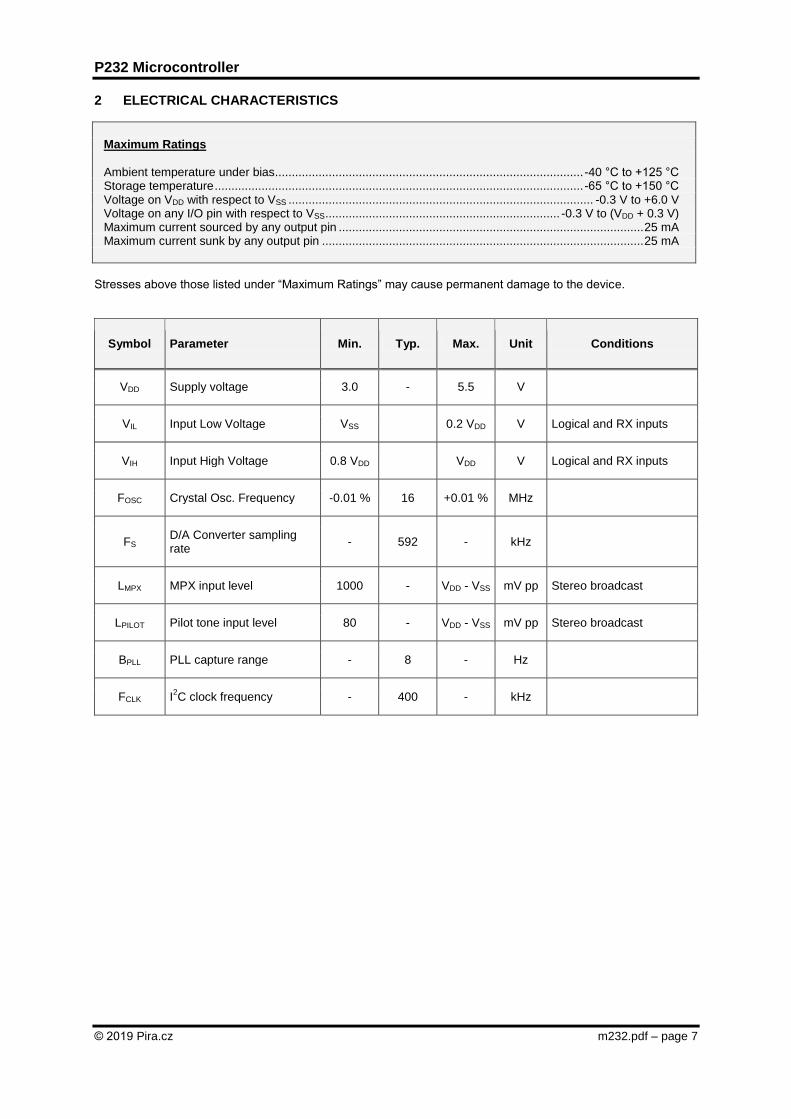
2 ELECTRICAL CHARACTERISTICS
Maximum Ratings
Ambient temperature under bias ............................................................................................ -40 °C to +125 °C Storage temperature .............................................................................................................. -65 °C to +150 °C Voltage on VDD with respect to VSS ........................................................................................... -0.3 V to +6.0 V Voltage on any I/O pin with respect to VSS ...................................................................... -0.3 V to (VDD + 0.3 V) Maximum current sourced by any output pin ........................................................................................... 25 mA Maximum current sunk by any output pin ................................................................................................ 25 mA
Stresses above those listed under “Maximum Ratings” may cause permanent damage to the device.
Symbol Parameter Min. Typ. Max. Unit Conditions
VDD Supply voltage 3.0 - 5.5 V
VIL Input Low Voltage VSS 0.2 VDD V Logical and RX inputs
VIH Input High Voltage 0.8 VDD VDD V Logical and RX inputs
FOSC Crystal Osc. Frequency -0.01 % 16 +0.01 % MHz
FS D/A Converter sampling rate
- 592 - kHz
LMPX MPX input level 1000 - VDD - VSS mV pp Stereo broadcast
LPILOT Pilot tone input level 80 - VDD - VSS mV pp Stereo broadcast
BPLL PLL capture range - 8 - Hz
FCLK I2C clock frequency - 400 - kHz
P232 Microcontroller
m232.pdf – page 8 © 2019 Pira.cz
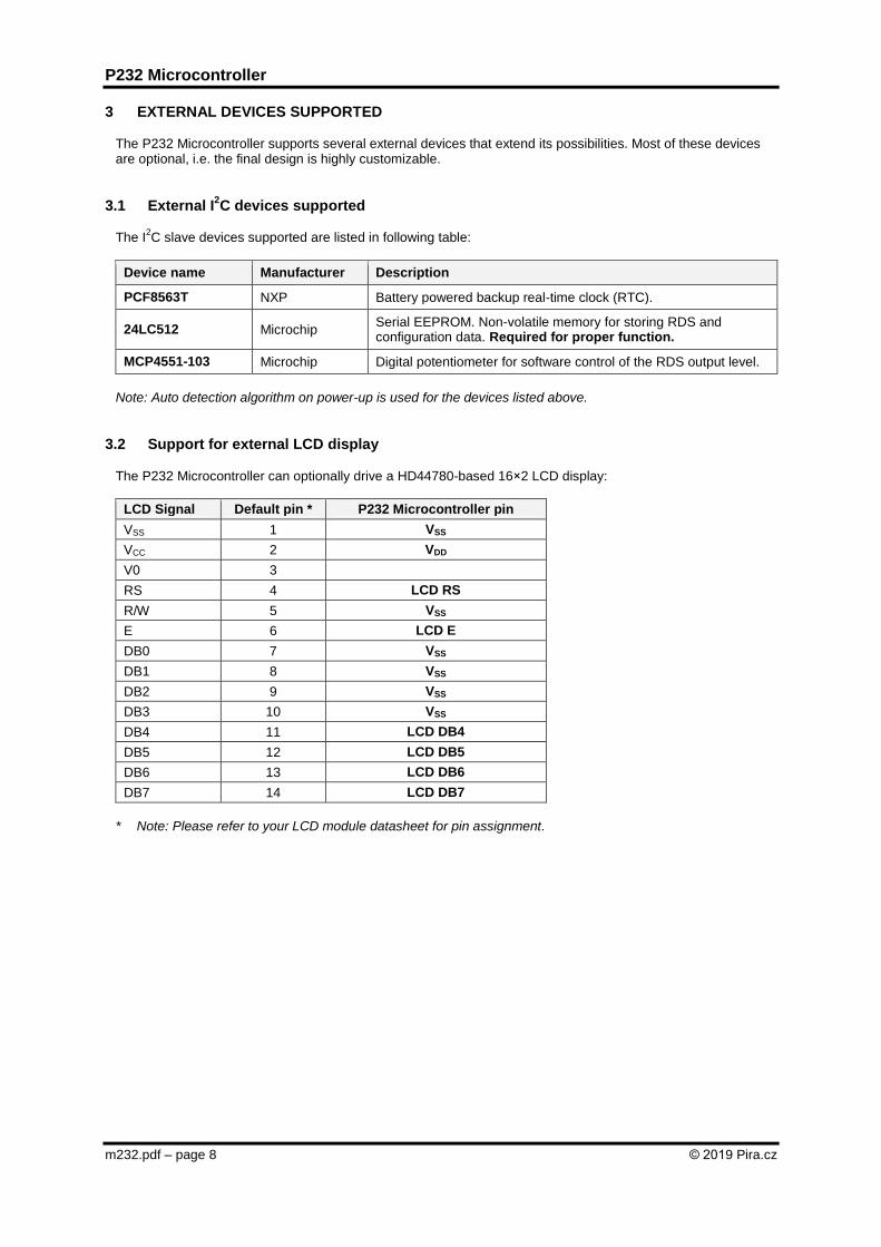
3 EXTERNAL DEVICES SUPPORTED
The P232 Microcontroller supports several external devices that extend its possibilities. Most of these devices are optional, i.e. the final design is highly customizable.
3.1 External I2C devices supported
The I
2C slave devices supported are listed in following table:
Device name Manufacturer Description
PCF8563T NXP Battery powered backup real-time clock (RTC).
24LC512 Microchip Serial EEPROM. Non-volatile memory for storing RDS and configuration data. Required for proper function.
MCP4551-103 Microchip Digital potentiometer for software control of the RDS output level.
Note: Auto detection algorithm on power-up is used for the devices listed above.
3.2 Support for external LCD display
The P232 Microcontroller can optionally drive a HD44780-based 16×2 LCD display:
LCD Signal Default pin * P232 Microcontroller pin
VSS 1 VSS
VCC 2 VDD
V0 3
RS 4 LCD RS
R/W 5 VSS
E 6 LCD E
DB0 7 VSS
DB1 8 VSS
DB2 9 VSS
DB3 10 VSS
DB4 11 LCD DB4
DB5 12 LCD DB5
DB6 13 LCD DB6
DB7 14 LCD DB7
* Note: Please refer to your LCD module datasheet for pin assignment.
P232 Microcontroller
© 2019 Pira.cz m232.pdf – page 9
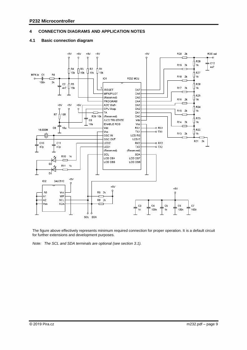
4 CONNECTION DIAGRAMS AND APPLICATION NOTES
4.1 Basic connection diagram
The figure above effectively represents minimum required connection for proper operation. It is a default circuit for further extensions and development purposes. Note: The SCL and SDA terminals are optional (see section 3.1).

P232 Microcontroller
m232.pdf – page 10 © 2019 Pira.cz
4.2 Design notes 4.2.1 Power supply
All power supply pins (VSS,VDD) must always be connected. The use of decoupling capacitors on every pair of power supply pins is required. Consider the following criteria when using decoupling capacitors:
Value and type of capacitor: A 0.1 F (100 nF), 10-20V capacitor is recommended. The capacitor should
be a low-ESR device, with a resonance frequency in the range of 200 MHz and higher. Ceramic capacitors are recommended.
Placement on the printed circuit board: The decoupling capacitors should be placed as close to the pins
as possible. It is recommended to place the capacitors on the same side of the board as the device. If space is constricted, the capacitor can be placed on another layer on the PCB using a via; however, ensure that the trace length from the pin to the capacitor is no greater than 0.25 inch (6 mm).
Handling high-frequency noise: Since the final equipment may experiencing high-frequency noise (upward
of tens of MHz), add a second ceramic type capacitor in parallel to the above described decoupling capacitor.
The value of the second capacitor can be in the range of 0.01 F to 0.001 F. Place this second capacitor next to each primary decoupling capacitor, closer to the Microcontroller.
Maximizing performance: On the board layout from the power supply circuit, run the power and return
traces to the decoupling capacitors first, and then to the device pins. This ensures that the decoupling capacitors are first in the power chain. Equally important is to keep the trace length between the capacitor and the power pins to a minimum, thereby reducing PCB trace inductance.
A low-ESR (< 5Ω) capacitor is required on the CPU VCAP pin to stabilize the internal voltage regulator voltage. The pin must not be connected to VDD and must use a capacitor of 10 μF connected to ground. The type can be
ceramic or tantalum. It is recommended that the trace length not exceed 0.25 inch (6 mm). 4.2.2 Hardware reset
The hardware reset is generated by holding the /RESET pin low. The device has a noise filter in the reset path which detects and ignores small pulses. A reset pulse is generated on-chip whenever VDD rises above a certain threshold. This allows the device to start in the initialized state when VDD is adequate for operation. To take advantage of this feature, tie the /RESET pin through a resistor (1k to 10k) to VDD. This will eliminate external RC components usually needed to create a reset delay. When the device starts normal operation (i.e., exits the reset condition), device operating parameters (voltage, temperature, etc.) must be met to ensure operation. If these conditions are not met, the device must be held in reset until the operating conditions are met. 4.2.3 Crystal oscillator
The oscillator circuit should be placed on the same side of the board as the device. Place the oscillator circuit close to the respective oscillator pins with no more than 0.5 inch (12 mm) between the circuit components and the pins. The load capacitors should be placed next to the oscillator itself, on the same side of the board. The load capacitor value depends on the crystal characteristics. Optimal value ensures the FOSC to lie in the tolerance range given in section Electrical characteristics. A good starting value is 47 pF for the load capacitors. 4.2.4 MPX/Pilot input and pilot PLL
The P232 Microcontroller includes an internal phase locked loop, which synchronises the RDS subcarrier with 19 kHz pilot tone in case of stereo broadcast. Parameters of the PLL are controlled by software. MPX signal or pilot tone is tied to the MPX/PILOT input pin. For the MPX signal, in order to keep the PLL performance, it is especially important not to exceed its signal level boundaries represented by power supply voltage. The pilot tone contained within the MPX signal must have at least the level equivalent to the parameter LPILOT minimum (see section Electrical characteristics). To meet these signal level requirements, if a wide range of input signal is expected on the MPX/PILOT pin, the signal should be pre-filtered using a simple 19 kHz bandpass filter. If there are spectrum components in the MPX signal above 60 kHz, these should be attenuated before feeding to the MPX/PILOT pin to prevent internal aliasing effect that can affect the PLL performance.

P232 Microcontroller
© 2019 Pira.cz m232.pdf – page 11
4.2.5 RS-232 interface (Port 1, Port 2)
The RS-232 interface is used on each port for the device configuration and data transfers. The RX and TX pin levels are compatible with TTL. For connection to external RS-232 equipment, an inverter and level converter is required (for example MAX232). For providing a USB connection, use a serial to USB converter IC (for example FT232). The serial data format is given in the RDS Encoder Technical manual (available online). The port characteristics are summarized in following table:
Port name I/O Pins Baudrate Initialization string * Readiness **
Port 1 RX1, TX1 Software configurable
1200 to 19200 bps Firmware version<CR><LF> 2500 ms
Port 2 RX2, TX2 Fixed at 19200 bps AT+i<CR><LF> 15 s
Notes: * The initialization string is a string send out of the device via TX pin on each power-up or reset. ** Time required after power-up or reset to get accepting incoming commands.
4.2.6 Digital-to-Analog converter
The P232 Microcontroller uses a parallel 8-bit D/A converter with over-sampling technique. Digital data provided on DA pins can be directly formed into final analogue RDS output signal using low-cost resistor network. Figure 4.2.6.1 shows accurate 8-bit DAC using R/2R resistor network. It’s a binary weighted DAC that creates each value with a repeating structure of 2 resistor values, R and R times two. This is an optimal DAC for this device. The resistor value tolerance must not exceed 2 %.
Figure 4.2.6.1 - 8-bit D/A converter R/2R network
P232 MCU
6
P232 Microcontroller
m232.pdf – page 12 © 2019 Pira.cz
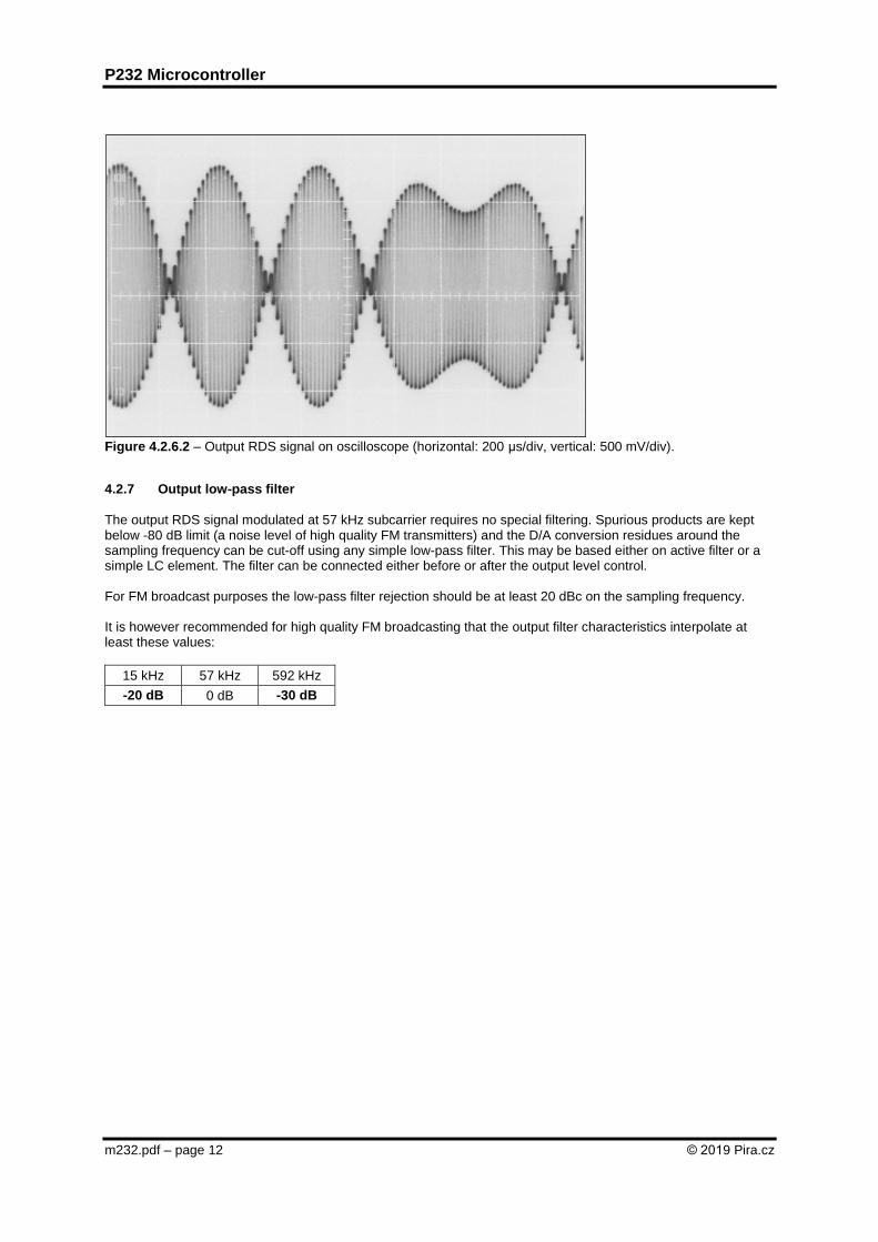
Figure 4.2.6.2 – Output RDS signal on oscilloscope (horizontal: 200 µs/div, vertical: 500 mV/div).
4.2.7 Output low-pass filter
The output RDS signal modulated at 57 kHz subcarrier requires no special filtering. Spurious products are kept below -80 dB limit (a noise level of high quality FM transmitters) and the D/A conversion residues around the sampling frequency can be cut-off using any simple low-pass filter. This may be based either on active filter or a simple LC element. The filter can be connected either before or after the output level control. For FM broadcast purposes the low-pass filter rejection should be at least 20 dBc on the sampling frequency. It is however recommended for high quality FM broadcasting that the output filter characteristics interpolate at least these values:
15 kHz 57 kHz 592 kHz
-20 dB 0 dB -30 dB

P232 Microcontroller
© 2019 Pira.cz m232.pdf – page 13
4.3 Typical applications (simplified block diagrams) 4.3.1 RDS Encoder with RS-232 and USB interface
4.3.2 RDS Encoder with RS-232 interface and independent control from embedded microcomputer
P232
Microcontroller
24LC512
(EEPROM)
PCF8563T
(RTC)
MCP4551
(Output level
control)
R/2R
low-cost
DAC
USB RS-232
LCD
MPX/Pilot
RDS
output
Port 2
Port 1
I2C
Level inverter
Serial to USB
adapter
P232
Microcontroller
Embedded
microcomputer
24LC512
(EEPROM)
PCF8563T
(RTC)
MCP4551
(Output level
control)
R/2R
low-cost
DAC
RS-232
LCD
MPX/Pilot
RDS
output
Port 2
Port 1
I2C
Level inverter
P232 Microcontroller
m232.pdf – page 14 © 2019 Pira.cz
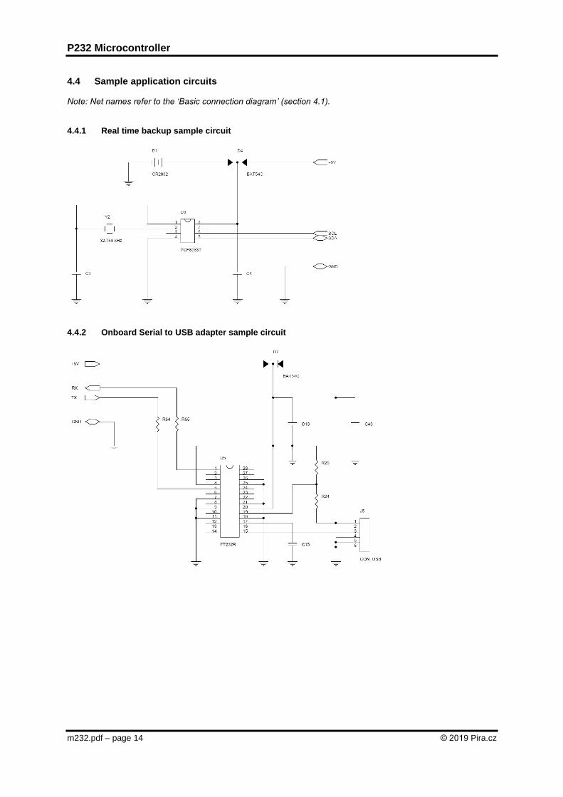
4.4 Sample application circuits Note: Net names refer to the ‘Basic connection diagram’ (section 4.1). 4.4.1 Real time backup sample circuit
4.4.2 Onboard Serial to USB adapter sample circuit

P232 Microcontroller
© 2019 Pira.cz m232.pdf – page 15
4.4.3 RDS level control circuit
4.4.4 Analog section sample circuit
Notes: J7 – Optional MPX or pilot tone input J3 – RDS or mixed output U6A section – Buffer providing low output impedance U6B section – 57kHz bandpass filter U7A section – MPX+RDS mixer U7B section – MPX/Pilot buffer and pre-filtering Output RDS level: software adjustable 0 to 4000 mVpp
P232 Microcontroller
m232.pdf – page 16 © 2019 Pira.cz
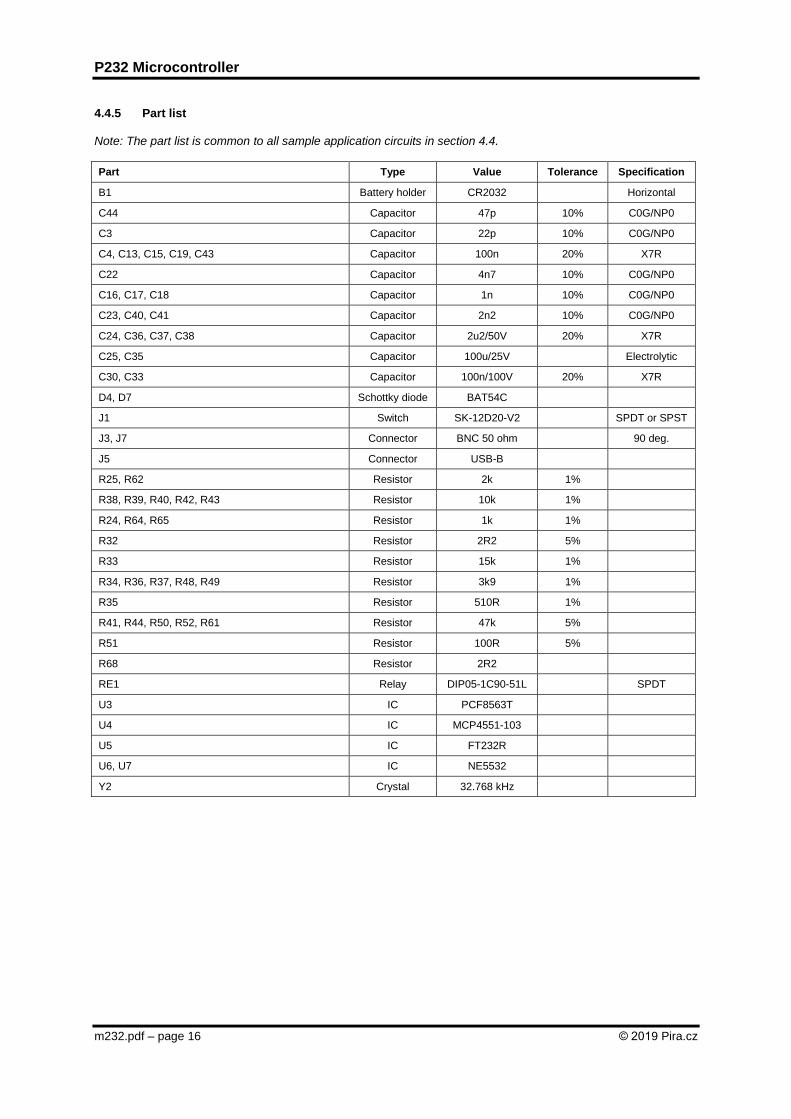
4.4.5 Part list
Note: The part list is common to all sample application circuits in section 4.4.
Part Type Value Tolerance Specification
B1 Battery holder CR2032 Horizontal
C44 Capacitor 47p 10% C0G/NP0
C3 Capacitor 22p 10% C0G/NP0
C4, C13, C15, C19, C43 Capacitor 100n 20% X7R
C22 Capacitor 4n7 10% C0G/NP0
C16, C17, C18 Capacitor 1n 10% C0G/NP0
C23, C40, C41 Capacitor 2n2 10% C0G/NP0
C24, C36, C37, C38 Capacitor 2u2/50V 20% X7R
C25, C35 Capacitor 100u/25V Electrolytic
C30, C33 Capacitor 100n/100V 20% X7R
D4, D7 Schottky diode BAT54C
J1 Switch SK-12D20-V2 SPDT or SPST
J3, J7 Connector BNC 50 ohm 90 deg.
J5 Connector USB-B
R25, R62 Resistor 2k 1%
R38, R39, R40, R42, R43 Resistor 10k 1%
R24, R64, R65 Resistor 1k 1%
R32 Resistor 2R2 5%
R33 Resistor 15k 1%
R34, R36, R37, R48, R49 Resistor 3k9 1%
R35 Resistor 510R 1%
R41, R44, R50, R52, R61 Resistor 47k 5%
R51 Resistor 100R 5%
R68 Resistor 2R2
RE1 Relay DIP05-1C90-51L SPDT
U3 IC PCF8563T
U4 IC MCP4551-103
U5 IC FT232R
U6, U7 IC NE5532
Y2 Crystal 32.768 kHz

P232 Microcontroller
© 2019 Pira.cz m232.pdf – page 17
5 PACKAGE DETAILS
5.1 40-Lead Plastic Dual In-Line (PDIP) 600 mil Body
Units INCHES
Dimension Limits MIN TYP MAX
Number of Pins N 40
Pitch e .100 BSC
Top to Seating Plane A - - .250
Molded Package Thickness A2 .125 - .195
Base to Seating Plane A1 .015 - -
Shoulder to Shoulder Width E .590 - .625
Molded Package Width E1 .485 - .580
Overall Length D 1.980 - 2.095
Tip to Seating Plane L .115 - .200
Lead Thickness c .008 - .015
Upper Lead Width b1 .030 - .070
Lower Lead Width b .014 - .023
Overall Row Spacing § eB - - .700
Notes:
1. Pin 1 visual index feature may vary, but must be located within the hatched area. 2. § Significant Characteristic. 3. Dimensions D and E1 do not include mold flash or protrusions. Mold flash or protrusions shall not
exceed .010” per side. BSC: Basic Dimension. Theoretically exact value shown without tolerances.
P232 Microcontroller
m232.pdf – page 18 © 2019 Pira.cz
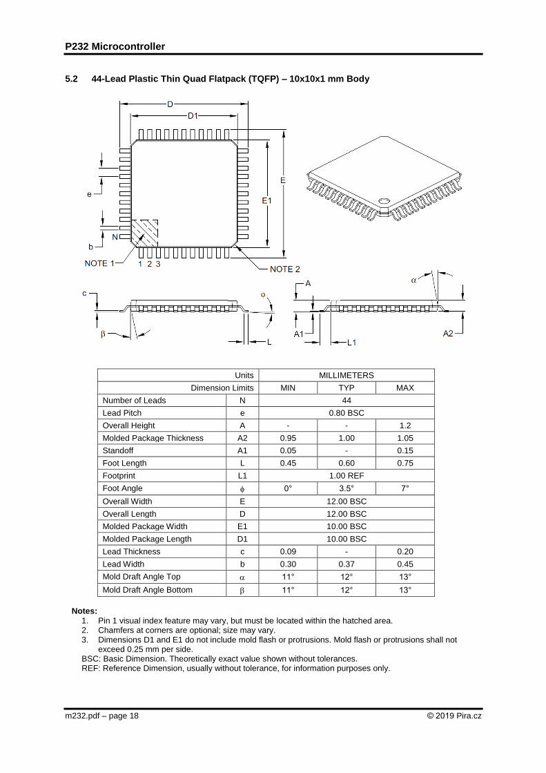
5.2 44-Lead Plastic Thin Quad Flatpack (TQFP) – 10x10x1 mm Body
Units MILLIMETERS
Dimension Limits MIN TYP MAX
Number of Leads N 44
Lead Pitch e 0.80 BSC
Overall Height A - - 1.2
Molded Package Thickness A2 0.95 1.00 1.05
Standoff A1 0.05 - 0.15
Foot Length L 0.45 0.60 0.75
Footprint L1 1.00 REF
Foot Angle 0° 3.5° 7°
Overall Width E 12.00 BSC
Overall Length D 12.00 BSC
Molded Package Width E1 10.00 BSC
Molded Package Length D1 10.00 BSC
Lead Thickness c 0.09 - 0.20
Lead Width b 0.30 0.37 0.45
Mold Draft Angle Top 11° 12° 13°
Mold Draft Angle Bottom 11° 12° 13°
Notes:
1. Pin 1 visual index feature may vary, but must be located within the hatched area. 2. Chamfers at corners are optional; size may vary. 3. Dimensions D1 and E1 do not include mold flash or protrusions. Mold flash or protrusions shall not
exceed 0.25 mm per side. BSC: Basic Dimension. Theoretically exact value shown without tolerances. REF: Reference Dimension, usually without tolerance, for information purposes only.