Pioneer DEH 2050MP
60
ORDER NO. PIONEER CORPORATION 4-1, Meguro 1-chome, Meguro-ku, Tokyo 153-8654, Japan PIONEER ELECTRONICS (USA) INC. P.O. Box 1760, Long Beach, CA 90801-1760, U.S.A. PIONEER EUROPE NV Haven 1087, Keetberglaan 1, 9120 Melsele, Belgium PIONEER ELECTRONICS ASIACENTRE PTE. LTD. 253 Alexandra Road, #04-01, Singapore 159936 PIONEER CORPORATION 2007 DEH-2050MP/XN/ES CRT4044 CD RECEIVER DEH-2050MP /XN/ES DEH-2050MPG /XN/ES DEH-2050MPG /XN/ES1 This service manual should be used together with the following manual(s): Model No. Order No. Mech.Module Remarks CX-3195 CRT3815 S10.5COMP2 CD Mech. Module : Circuit Descriptions, Mech. Descriptions, Disassembly For details, refer to "Important Check Points for Good Servicing". K-ZZU. OCT. 2007 Printed in Japan
-
Upload
pocho-pochito -
Category
Documents
-
view
716 -
download
54
Transcript of Pioneer DEH 2050MP

PIONEER CORPORATION 4-1, Meguro 1-chome,PIONEER ELECTRONICS (USA) INC. P.O. Box 1760, LonPIONEER EUROPE NV Haven 1087, Keetberglaan 1, 912PIONEER ELECTRONICS ASIACENTRE PTE. LTD. 253
PIONEER CORPORATION 2007
DEH-2050MP/XN/ES
Meguro-ku, Tokyo 153-8654, Japang Beach, CA 90801-1760, U.S.A.0 Melsele, BelgiumAlexandra Road, #04-01, Singapore 159936
ORDER NO.
CRT4044
CD RECEIVER
DEH-2050MP/XN/ES
DEH-2050MPG/XN/ES
DEH-2050MPG/XN/ES1
This service manual should be used together with the following manual(s):
Model No. Order No. Mech.Module Remarks
CX-3195 CRT3815 S10.5COMP2 CD Mech. Module : Circuit Descriptions, Mech. Descriptions, Disassembly
For details, refer to "Important Check Points for Good Servicing".
K-ZZU. OCT. 2007 Printed in Japan

C
D
F
A
B
E
1 2 3 4
SAFETY INFORMATION
- Safety Precautions for those who Service this Unit.
When checking or adjusting the emitting power of the laser diode exercise caution in order to get safe, reliable
results.
Caution:
1. During repair or tests, minimum distance of 13 cm from the focus lens must be kept.
2. During repair or tests, do not view laser beam for 10 seconds or longer.
CAUTIONDanger of explosion if battery is incorrectly replaced.Replaced only with the same or equivalent type recommended by the manufacture.Discord used batteries according to the manufacture's instructions.
This service manual is intended for qualified service technicians; it is not meant for the casual do-it-yourselfer.Qualified technicians have the necessary test equipment and tools, and have been trained to properly and safelyrepair complex products such as those covered by this manual.Improperly performed repairs can adversely affect the safety and reliability of the product and may void the warranty.If you are not qualified to perform the repair of this product properly and safely, you should not risk trying to do soand refer the repair to a qualified service technician.
DEH-2050MP/XN/ES21 2 3 4

C
D
F
A
B
E
5 6 7 8
[Important Check Points for Good Servicing]In this manual, procedures that must be performed during repairs are marked with the below symbol.Please be sure to confirm and follow these procedures.
1. Product safety
Please conform to product regulations (such as safety and radiation regulations), and maintain a safe servicing environment by following the safety instructions described in this manual.
1 Use specified parts for repair.
Use genuine parts. Be sure to use important parts for safety.
2 Do not perform modifications without proper instructions.
Please follow the specified safety methods when modification(addition/change of parts) is required due to interferences such as radio/TV interference and foreign noise.
3 Make sure the soldering of repaired locations is properly performed.
When you solder while repairing, please be sure that there are no cold solder and other debris.Soldering should be finished with the proper quantity. (Refer to the example)
4 Make sure the screws are tightly fastened.
Please be sure that all screws are fastened, and that there are no loose screws.
5 Make sure each connectors are correctly inserted.
Please be sure that all connectors are inserted, and that there are no imperfect insertion.
6 Make sure the wiring cables are set to their original state.
Please replace the wiring and cables to the original state after repairs.In addition, be sure that there are no pinched wires, etc.
7 Make sure screws and soldering scraps do not remain inside the product.
Please check that neither solder debris nor screws remain inside the product.
8 There should be no semi-broken wires, scratches, melting, etc. on the coating of the power cord.
Damaged power cords may lead to fire accidents, so please be sure that there are no damages.If you find a damaged power cord, please exchange it with a suitable one.
9 There should be no spark traces or similar marks on the power plug.
When spark traces or similar marks are found on the power supply plug, please check the connection and advise on secure connections and suitable usage. Please exchange the power cord if necessary.
a Safe environment should be secured during servicing.
When you perform repairs, please pay attention to static electricity, furniture, household articles, etc. in order to prevent injuries. Please pay attention to your surroundings and repair safely.
2. Adjustments
To keep the original performance of the products, optimum adjustments and confirmation of characteristics within specification.Adjustments should be performed in accordance with the procedures/instructions described in this manual.
4. Cleaning
For parts that require cleaning, such as optical pickups, tape deck heads, lenses and mirrors used in projection monitors, proper cleaning should be performed to restore their performances.
3. Lubricants, Glues, and Replacement parts
Use grease and adhesives that are equal to the specified substance. Make sure the proper amount is applied.
5. Shipping mode and Shipping screws
To protect products from damages or failures during transit, the shipping mode should be set or the shipping screws should be installed before shipment. Please be sure to follow this method especially if it is specified in this manual.
DEH-2050MP/XN/ES 35 6 7 8

C
D
F
A
B
E
1 2 3 4
CONTENTS SAFETY INFORMATION..................................................................................................................................... 21. SERVICE PRECAUTIONS ............................................................................................................................... 5
1.1 SERVICE PRECAUTIONS......................................................................................................................... 51.2 NOTES ON SOLDERING .......................................................................................................................... 5
2. SPECIFICATIONS ............................................................................................................................................ 62.1 SPECIFICATIONS...................................................................................................................................... 62.2 DISC/CONTENT FORMAT ........................................................................................................................ 62.3 PANEL FACILITIES.................................................................................................................................... 72.4 CONNECTION DIAGRAM ......................................................................................................................... 8
3. BASIC ITEMS FOR SERVICE.......................................................................................................................... 93.1 CHECK POINTS AFTER SERVICING....................................................................................................... 93.2 PCB LOCATIONS .................................................................................................................................... 103.3 JIGS LIST ................................................................................................................................................ 11
4. BLOCK DIAGRAM.......................................................................................................................................... 124.1 BLOCK DIAGRAM ................................................................................................................................... 12
5. DIAGNOSIS.................................................................................................................................................... 165.1 OPERATIONAL FLOW CHART ............................................................................................................... 165.2 ERROR CODE LIST ................................................................................................................................ 175.3 CONNECTOR FUNCTION DESCRIPTION............................................................................................. 18
6. SERVICE MODE ............................................................................................................................................ 196.1 CD TEST MODE...................................................................................................................................... 196.2 CHECKING THE GRATING AFTER CHANGING THE PICKUP UNIT.................................................... 21
7. DISASSEMBLY............................................................................................................................................... 238. EACH SETTING AND ADJUSTMENT ........................................................................................................... 26
8.1 PCL OUTPUT CONFIRMATION.............................................................................................................. 269. EXPLODED VIEWS AND PARTS LIST.......................................................................................................... 26
9.1 PACKING ................................................................................................................................................. 269.2 EXTERIOR............................................................................................................................................... 289.3 CD MECHANISM MODULE..................................................................................................................... 30
10. SCHEMATIC DIAGRAM ............................................................................................................................... 3210.1 OVERALL CONNECTION DIAGRAM(GUIDE PAGE)............................................................................ 3210.2 KEYBOARD UNIT.................................................................................................................................. 3810.3 CD MECHANISM MODULE(GUIDE PAGE) .......................................................................................... 4010.4 WAVEFORMS........................................................................................................................................ 46
11. PCB CONNECTION DIAGRAM ................................................................................................................... 4811.1 TUNER AMP UNIT................................................................................................................................. 4811.2 KEYBOARD UNIT.................................................................................................................................. 5211.3 CD CORE UNIT(S10.5COMP2)............................................................................................................. 54
12. ELECTRICAL PARTS LIST .......................................................................................................................... 56
DEH-2050MP/XN/ES41 2 3 4

C
D
F
A
B
E
5 6 7 8
1. SERVICE PRECAUTIONS1.1 SERVICE PRECAUTIONS
1.2 NOTES ON SOLDERING
- Service Precaution1. You should conform to the regulations governing the product (safety, radio and noise, and other regulations), and should keep the safety during servicing by following the safety instructions described in this manual.2. Before disassembling the unit, be sure to turn off the power. Unplugging and plugging the connectors during power-on mode may damage the ICs inside the unit.3. To protect the pickup unit from electrostatic discharge during servicing, take an appropriate treatment (shorting-solder) by referring to "the DISASSEMBLY".4. After replacing the pickup unit, be sure to check the grating.5. Be careful in handling ICs. Some ICs such as MOS type are so fragile that they can be damaged by electrostatic induction.
For environmental protection, lead-free solder is used on the printed circuit boards mounted in this unit. Be sure to use lead-free solder and a soldering iron that can meet specifications for use with lead-free solders for repairs accompanied by reworking of soldering.
Compared with conventional eutectic solders, lead-free solders have higher melting points, by approximately 40 C. Therefore, for lead-free soldering, the tip temperature of a soldering iron must be set to around 373 C in general, although the temperature depends on the heat capacity of the PC board on which reworking is required and the weight of the tip of the soldering iron.
Compared with eutectic solders, lead-free solders have higher bond strengths but slower wetting times and higher melting temperatures (hard to melt/easy to harden).
The following lead-free solders are available as service parts: Parts numbers of lead-free solder: GYP1006 1.0 in dia. GYP1007 0.6 in dia. GYP1008 0.3 in dia.
DEH-2050MP/XN/ES 55 6 7 8

C
D
F
A
B
E
1 2 3 4
2. SPECIFICATIONS2.1 SPECIFICATIONS
2.2 DISC/CONTENT FORMAT
Backup current...................................... 2 mA or less
DEH-2050MP/XN/ES61 2 3 4

C
D
F
A
B
E
5 6 7 8
2.3 PANEL FACILITIES
DEH-2050MP/XN/ES 75 6 7 8

C
D
F
A
B
E
1 2 3 4
2.4 CONNECTION DIAGRAM- Connection Diagram
DEH-2050MP/XN/ES81 2 3 4

C
D
F
A
B
E
5 6 7 8
3. BASIC ITEMS FOR SERVICE3.1 CHECK POINTS AFTER SERVICING
To keep the product quality after servicing, please confirm following check points.
No. Procedures Item to be confirmed1 Confirm whether the customer complain has been
solved.If the customer complain occurs with the specificmedia, use it for the operation check.
The customer complain must not be reappeared.Display, audio and operations must be normal.
2 CD Play back a CD.(Track search)
No malfunction on display, audio and operation.Display, audio and operations must be normal.
3 FM/AM tuner Check FM/AM tuner action.(Seek, Preset)Switch band to check both FM and AM.
Display, audio and operations must be normal.
4 Check whether no disc is inside the product. The media used for the operating check must beejected.
5 Appearance check No scratches or dirt on its appearance afterreceiving it for service.
See the table below for the items to be checked regarding video and audio:
Item to be checked regarding audioDistortionNoiseVolume too lowVolume too highVolume fluctuatingSound interrupted
DEH-2050MP/XN/ES 95 6 7 8

C
D
F
A
B
E
1 2 3 4
3.2 PCB LOCATIONS
A
B
C
Unit Number : YWM5234 Unit Name : Tuner Amp Unit Unit Number : (2050MP/XN/ES)Unit Name : Keyboard Unit Unit Number : (2050MPG/XN/ES)Unit Number : (2050MPG/XN/ES1)Unit Name : Keyboard Unit Unit Number : CWX3514 Unit Name : CD Core Unit(S10.5COMP2)
CD Core Unit(S10.5)
Keyboard Unit
Tuner Amp Unit
DEH-2050MP/XN/ES101 2 3 4
C
D
F
A
B
E
5 6 7 8
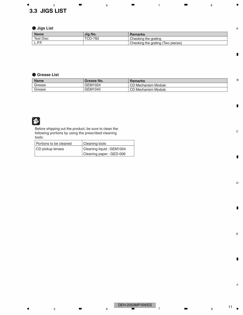
3.3 JIGS LIST
Before shipping out the product, be sure to clean the following portions by using the prescribed cleaning tools:
Portions to be cleaned Cleaning tools
CD pickup lenses Cleaning liquid : GEM1004Cleaning paper : GED-008
- Jigs List NameTest DiscL.P.F.
Jig No.TCD-782
RemarksChecking the gratingChecking the grating (Two pieces)
Name Jig No. Remarks
- Grease List NameGreaseGrease
Grease No.GEM1024GEM1045
RemarksCD Mechanism ModuleCD Mechanism Module
Name Grease No. Remarks
DEH-2050MP/XN/ES 115 6 7 8

C
D
F
A
B
E
IN1_L
IN2_L
1
ELECSOU
2
FF
-IN
A
B
EFA
EFB
ET
K
E1
O
E2
LOUT
IC 601(2PN5012
YSTEM MCOMPUT
1 2 3 4
4. BLOCK DIAGRAM4.1 BLOCK DIAGRAM
PICKUP UNIT(P10.5)(SERVICE) D
CD CORE UNIT(S10.5COMP2)C
BRST,BRXEN,BSRQ
CN701Q101
M
LASERDIODE
MONITORDIODE
S903DSCSNS
SPINDLEMOTOR
MCARRIAGEMOTOR
LOAD/
LD-
MD
15
5
HOLOGRAM UNIT
IC301BA5839FP IC201
PE5547A
RF-AMP, CD DECODER, MP3/WMA DECODER,
DIGITAL SERVO / DATA PROCESSOR
CDDRIVER
2VD
VD
13LOUT
9
CN101
16SOP
15SOM
18LCOP
17LCOM
21CLCONT
55LOUT
9CONT
TD,FD
AC,BD,F,E
SD,MD
S901HOME
S90412EJ
S9058EJ
LD+ 14
141LD
142PD
12EJ
CONT
CLCONT
HOME
8
9
43
41
VDD
1
VDD
BDATA,BSCK
Q102
39/PUEN
VDD
15
5
FOCUS ACT.TRACKING ACT.
FOP
TOP21 TOP
FOP
11 FOP14 TOP
21
14
8EJ7
DSCSNS6
VCC
16/RESET 8/RESET
88VREFREFO 133
REFOUT
33FOM FOM
12 FOM
44TOM TOM
13 TOM
22LOEJ LOEJ5
52
50
X201
XTAL
/XTAL16.93MHz
VDSENS11
VD
TUNL
CN4011
2
CN651
TUNER AMP UNIT
LOUT
ASYS+B
ANTENNA
IFA
IFB
CDRESET
3
B.UP
VDD
5
VD
Q991
14
7
SWVDD
SWD5V6
5
IC 911BA4918-V12
BSENS
TOP41
POWERO2
1
36
47
15
SWVDD4 1
15Q992
BRST,BRXEN,BSRQ,BDATA,BSCK
8RESET 16
FM/AM TUNER UNIT
AM
_AN
T
SL-
IN
RE
FA
RE
FB
LDE
T
SWVDD
DI
CK
CE
1
DO
CE
2
SLO
UT
SL
IF
IF
R
R
LD
DI
C
C
D
C
S
PDL3126
CD VD
CDL
3
REGULATOR IC
B.UP10
9VDD
SYS+B8
7
S
SYSPW
DREG85
SWVDD
Q601
PLL_VDD
DVDD3
REGC(M)55
9
57
DVDD294
DVDD4121
VD
ATTATT
TANK
ATT RF LFP
LFPVCO
CF
IC1MIX / IF / PLL
IC2EEPROM
1 2 3 4 5 6 7 8 9 10 12 13 14 15 16 17 18 19 2011A
NT
VC
C
SLI
N
IFO
UT
A
IFO
UT
B
DG
ND
RE
FIN
A
RE
FIN
B
LDE
T
VD
D DI
CK
CE
1
DO
CE
2
SLO
UT
RF
GN
D1
RF
GN
D2
RF
GN
D3
RF
GN
D4
DEH-2050MP/XN/ES121 2 3 4

C
D
F
A
B
E
TUNL
CDRESET
BSENS
TOP41
POWEROF
SWVDD
SL-
IFA
IFB
RE
RE
LDE
DI
CK
CE
DO
CE
SLO
PDL3
CDL
SYC
DREG
PLL_VDD
DVDD3
REGC(M)
DVDD2
DVDD4
5 6 7 8
IN1_L
IN2_L
1
IC 151PML014A
ELECTRONIC VOLUME/SOURCE SELECTOR
2
7Rear_L
B.UP
35
44MUTE
21
23
3
5
VCC
VCC
FL
FL
RL
RL
FL
FL
RL
RL
B.REMOTE
ACC
22
AMPIC 301
PAL007C
Q931
MUTE
CN831
VC
K, V
DT
, VS
T
Q201(1/2)
Q201(2/2)
B.UP
Q821
SYSTEM MICROCOMPUTER
ACC SENSE
3
9
11
12
10
1
2
CN901
9
10
11
4
13
14
12
SOURCE
DSENS
ILM+B
ROT1
ROT0
DPDT
KYDT
SRC33
34
ILMPW2
VCK111
VDT110
DPDT/SELF23
KEYDT/SELF24
CN351
RLIn12
DSENS
Q822
ASENS
6Front_L FLIn
14
XOUT
XIN
82
X60174.1MHz81
Q351
MUTE
20
6
25NC/BREM
ASENS
2RL
6
F
SL-62IN
IF_INA77
IF_INB78
FREF_A96FA
FREF_B97FB
LOCK99T
DI100
CK101
CE1021
DO103
VST1092
ADIN7136UT
L_OUT59
IC 601(2/2)PN5012B
STEM MICROOMPUTER
4STBY
B.UP
AUX-G6
AUX-L7
AUX-L4
AUX-G5IN4+_L
IN4-_L
ILMPW
MUTE
BU_X1
BU_X2
52
X6024.7186MHz51
SRC
DSENS
ILL+B
ROT1
ROT0
DPDT
KYDT
IC 1801PD6340A
LCD DRIVER/KEY CONTROLLER
KEY DATA
LCD1801
CN1801
KEYBOARD UNIT
10
11
18
20
DPDT
KYDT
B
13
12
D1803-D1810D1812-D1823D1825
3SWVDDSWD5V 3 SWVDD
SWVDD
4
X0
X1
22
X18015MHz23
KEY MATRIX
1056
VLCDVDD
9
14
VOLUME
S18311
2
SOURCE
S1830
6
7
CN1802
AUX G
AU
X L
AU
X G
AUX L
AUX IN21
IC 601(1/2)PN5013B
FL
RL
3
9
11
12
10
1
6
2
BACK UP
GND
ACC
B.REM
DEH-2050MP/XN/ES 135 6 7 8

C
D
F
A
B
E
1 2 3 4
No. Symbol I/O Explain1 ANT I Antenna Input Antenna input. 75 ohm. Surge absorber is necessary.
Series circuit including an inductor and a resistor is connected with RF ground for the countermeasure against the ham of power transmission line.
2 RFGND1 RF Ground Ground of R.F. block3 RFGND2 RF Ground Ground of R.F. block 4 RFGND3 RF Ground Ground of R.F. block5 RFGND4 RF Ground Ground of R.F. block6 VCC Power Supply Power supply for Analog block. D.C 8.4 V + 0.3 V
(performance isn't guaranteed besides 8.4 V)7 SLIN I Signal Level Input Input signa level from BE_IC8 IFOUTA
IFOUTBOO
IF Output IF signal output (F.E.output)9 IF Output IF signal output (F.E.output)
10 DGND Digital Ground Ground of Digital. block11 REFINA I
I
I
I
I
Reference Signal Input reference signal for PLL part with FE_IC 12 REFINB Reference Signal Input reference signal for PLL part with FE_IC 13 LDET Lock Detector PLL lock detecter output "High" active14 VDD
OPower Supply Power supply for Digital block. D.C 3.3 V + 0.2 V
15 DI Data In
16 CK CK
17 CE1 Chip Enable-1 Chip enable for FE_IC "High" active18 DO O Data Out Data output19 CE2 O Chip Enable-2
20 SLOUT O Signal Level Output Output of FM/AM signals level (D.C.)
- FM/AM Tuner Unit
Clock data input(not sending data in tuner reception operating in noise being output)
Data input (not sending data in tuner reception operating in noise being output)
Chip enable for EEPROM "Low" active. in power ON/OFF, please turn CE2 into "High" (= VDD).
ATTATT
TANK
ATT RF LFP
LFPVCO
CF
IC1MIX / IF / PLL
IC2EEPROM
1 2 3 4 5 6 7 8 9 10 12 13 14 15 16 17 18 19 2011
AN
T
VC
C
SLI
N
IFO
UT
A
IFO
UT
B
DG
ND
RF
INA
RF
INB
LDE
T
VD
D
DI
CK
CE
1
DO
CE
2
SLO
UT
RF
GN
D1
RF
GN
D2
RF
GN
D3
RF
GN
D4
DEH-2050MP/XN/ES141 2 3 4
C
D
F
A
B
E
5 6 7 8
- LCD(CAW1930)
SE
GM
EN
T
CO
MM
ON
DEH-2050MP/XN/ES 155 6 7 8

C
D
F
A
B
E
1 2 3 4
5. DIAGNOSIS5.1 OPERATIONAL FLOW CHART
SWVDD
VDDPin 8
Power ON
bsens = L
asens = L
bsensPin 36
asensPin 35
HPin 1
Source keys operative
Completes power-on operation.(After that, proceed to each source operation.)
SYSPW HPin 15
Starts communication with Grille microcomputer.
Source ON
300 ms
300 ms
In case of the above signal, the communication with Grille microcomputer may fail.If the time interval is not 300 msec, the oscillator may be defective.
DEH-2050MP/XN/ES161 2 3 4

C
D
F
A
B
E
5 6 7 8
5.2 ERROR CODE LIST- Error Messages
If a CD is not operative or stopped during operation due to an error, the error mode is turned on and cause(s) of the error is indicated with a corresponding number. This arrangement is intended at reducing nonsense calls from the users and also for facilitating trouble analysis and repair work in servicing.
(1) Basic Indication Method
1) When SERRORM is selected for the CSMOD (CD mode area for the system), error codes are written to DMIN (minutes display area) and DSEC (seconds display area). The same data is written to DMIN and DSEC. DTNO remains in blank as before.
2) Head unit display examples
Depending on display capability of LCD used, display will vary as shown below. xx contains the error number.
8-digit display 6-digit display 4-digit display
ERROR-xx ERR-xx E-xx
(2) Error Code List
Code Class Displayed error code Description of the code and potential cause(s)
10 Electricity Carriage Home NG CRG can't be moved to inner diameter.
SERVO LSI Com- CRG can't be moved from inner diameter.
munication Error → Failure on home switch or CRG move mechanism.
Communication error between microcomputer and SERVO LSI.
11 Electricity Focus Servo NG Focusing not available.
→ Stains on rear side of disc or excessive vibrations on REWRITABLE.
12 Electricity Spindle Lock NG Spindle not locked. Sub-code is strange (not readable).
Subcode NG → Failure on spindle, stains or damages on disc, or excessive vibrations.
A disc not containing CD-R data is found.
Turned over disc are found, though rarely.
CD signal error.
17 Electricity Setup NG AGC protection doesn't work. Focus can be easily lost.
→ Damages or stains on disc, or excessive vibrations on REWRITABLE.
30 Electricity Search Time Out Failed to reach target address.
→ CRG tracking error or damages on disc.
44 Electricity ALL Skip Skip setting for all track.
(CD-R/RW)
50 Mechanism CD On Mech Error Mechanical error during CD ON.
→ Defective loading motor, mechanical lock and mechanical sensor.
A0 System Power Supply NG Power (VD) is ground faulted.
→ Failure on SW transistor or power supply (failure on connector).
Remarks: Mechanical errors are not displayed (because a CD is turned off in these errors).
Unreadable TOC does not constitute an error. An intended operation continues in this case.
Upper digits of an error code are subdivided as shown below:
1x: Setup relevant errors, 3x: Search relevant errors, Ax: Other errors.
DEH-2050MP/XN/ES 175 6 7 8

C
D
F
A
B
E
1 2 3 4
5.3 CONNECTOR FUNCTION DESCRIPTION
Pin No.12345678
B. UPGNDACCNCNCB.REMNCTEL
Pin No.9
10111213141516
RL-FL-RL+FL+RR-FR-RR+FR+
ANTENNA REAR OUTPUT
1615
1413
1211
109
87
65
43
21
DEH-2050MP/XN/ES181 2 3 4

C
D
F
A
B
E
5 6 7 8
6. SERVICE MODE6.1 CD TEST MODE
1) Cautions on adjustments• In this product the single voltage (3.3 V) is used for the regulator. The reference voltage is the REFO1 (1.65 V) instead of the GND.If you should mistakenly short the REFO1 with the GND during adjustment, accurate voltage will not be obtained, and the servo’s misoperation will apply excessive shock to the pickup. To avoid such problems:a. Do not mix up the REFO1 with the GND when connecting the (-) probe of measuring instruments. Especially on an oscilloscope, avoid connecting the (-) probe for CH1 to the GND. b. In many cases, measuring instruments have the same potential as that for the (-) probe. Be sure to set the measuring instruments to the floating state.c. If you have mistakenly connected the REFO1 to the GND, turn off the regulator or the power immediately.
• Before mounting and removing filters or leads for adjustment, be sure to turn off the regulator.
• For stable circuit operation, keep the mechanism operating for about one minute or more after the regulator is turned on.
• In the test mode, any software protections will not work. Avoid applying any mechanical or electrical shock to the mechanism during adjustment.
• The RFI and RFO signals with a wide frequency range are easy to oscillate. When observing the signals, insert a resistor of 1k ohms in series.
• The load and eject operation is not guarantied with the mechanism upside down. If the mechanism is blocked due to mistaken eject operation, reset the product or turn off and on the ACC to restore it.
2) Test modeThis mode is used to adjust the CD mechanism module.• To enter the test mode.While pressing the 4 and 6 keys at the same time, reset.• To exit from the test mode.Turn off the ACC and back up.
Notes:a. During ejection, do not press any other keys than the EJECT key until the loaded disc is ejected.b. If you have pressed the (→) key or (←) key during focus search, turn off the power immediately to protect the actuator from damage caused by the lens stuck.c. For the TR jump modes except 100TR, the track jump operation will continue even if the key is released.d. For the CRG move and 100TR jump modes, the tracking loop will be closed at the same time when the key is released.e. When the power is turned off and on, the jump mode is reset to the single TR (91), the RF amp gain is set to 0 dB, and the auto-adjustment values are reset to the default settings.
DEH-2050MP/XN/ES 195 6 7 8

C
D
F
A
B
E
1 2 3 4
[Key]
Contents
Display
[4] + [6] + Reset or[4] + [6] + BU + ACC
Test Mode In
[CD] or [SOURCE]
Source On
TRK MIN SEC
[BAND]
Power On(T.Offset is adjusted)TRK MIN SEC00 00 00
[3]
Power On(T.Offset is not adjusted)
99 99 99
[2]
RF AMPGain switching
GG GG GG
*1[4]
SPINDLESpeed switching
SP SP SP
*9
[3]
Focus CloseS curve check
TRK MIN SEC91 91 91
[6]
Focus Mode switching
0X 0X 0X
*2
[1]
Tracking ServoClose
00 00 00or 99 99 99
[>]
CRG +
[2]
Self-adjustingswitching
TRK MIN SEC?? ?? ??
*3*8
[<]
CRG -*8
[BAND]
Power Off
TRK MIN SEC
[BAND]
Power Off
TRK MIN SEC
[BAND]
Power Off
TRK MIN SEC
[BAND]
Power Off
TRK MIN SEC
[1]T.Close & AGC
Applicable servomechanism
TRK MIN SEC?tr ?min ?sec
[6] [3]
RF AGC /RF AGC coefficient display
[>]
CRG +
8X 8X 8Xor 9X 9X 9X
[2]
T.Balance adjustment /T.BAL coefficient display
TRK MIN SEC?? ?? ??
[<]
CRG -T.CloseApplicable servomechanism
?? ?? ??
[1]
F,T,RF AGCF.Bias display switchingTRK MIN SEC
TRK MIN SEC
TRK MIN SEC
TRK MIN SEC?tr ?min ?sec
TRK MIN SEC
[3] [6]
CRG/TR jumpvalue switching
[>]
CRG/TR Jump +
[2]
Tracking Open
[<]
CRG/TR Jump -
?tr ?min ?sec
TRK MIN SEC
TRK MIN SEC
TRK MIN SEC?tr ?min ?sec
00 00 00or 99 99 99
TRK MIN SEC
TRK MIN SEC?tr ?min ?sec
8X 8X 8Xor 9X 9X 9X
8X 8X 8Xor 9X 9X 9X
00 00 00or 99 99 99
TRK MIN SEC?tr ?min ?sec?? ?? ??
*7 F,T AGC / F.BiasRF AGC
8X 8X 8Xor 9X 9X 9X
[2]
Tracking Open
*6
*5
*4 *4
Operation[Key] Test Mode
[BAND] Power On/Off[>] CRG + / TR Jump +
(Direction of the external surface)[<] CRG - / TR Jump -
(Direction of the internal surface)[1] T. CLS & AGC & Applicable servomechanism /
AGC,AGC display setting[2] RF Gain switching / Offset adjustment display /
T.Balance adjustment / T. Open[3] F. Close,S Curve / Rough Servo and RF AGC /
F,T,RF AGC[4] SPDL 1X/2X switching
As for the double speed(2x), audio output cannot besupported.
[5] Error Rate measurementON : ERR 30Counts StartBER display data[%]
[6] F. Mode switching / Tracking Close / CRG•TRJump Switching
*) • After the [Eject] key is pressed keys other than the [Eject] key should not be pressed, until disc ejection is complete.• When the key [2] or [3] is pressed during the Focus Search, the power supply should be immediately turned off (otherwise the lens
sticks to Wall, causing the actuator to be damaged).• In the case of TR jump other than to 100TR, the function shall continue to be processed even if the TR jump key is released. As for
the CRG Move and 100TR Jump, the mechanism shall be set to the Tracking Close mode when the key is released.• When the power is turned on/off the jump mode is reset to the Single TR (91) while the gain of the RFAMP is reset to 0 dB. At the
same time all the self-adjusting values shall return to the default setting.
*10
TRK MIN SEC
[5]
Gop ModeGop Mode switching
OL OL OL
- Flow Chart
*1) TYP → + 6 dB → + 12 dB TRK MIN SEC TRK06MIN06SEC06 TRK12MIN12SEC12
*2) Focus Close → S Curve check setting → F EQ measurement setting TRK00MIN00SEC00
TRK01MIN01SEC01 TRK02MIN02SEC02 (TRK99MIN99SEC99)
*3) F.Offset Display → RF.Offset → T.Offset Display → Switch to the order of the original display
*4) 1TR/4TR/10TR/32TR/100TR*5) Single → 4TR → 10TR → 32TR → 100TR → CRG Move 9x(8x):91(81) 92(82) 93(83) 94(84) 95(85) 96(86)
*6) Only at the time of CRG move, 100TR jump
*7) TRK/MIN/SEC → F.AGC → T.AGC Gain → F.Bias → RF AGC
*8) CRG motor voltage = 2 [V]
*9) TYP (1X) → 2X → 1X TRK MIN SEC
TRK22MIN22SEC22 TRK11MIN11SEC11*10) OFF(TYP) → FORCUS → TRACKING TRK MIN SEC
TRK70MIN70SEC70 TRK71MIN71SEC71
• As for the double speed (2x), audio output cannot be supported
DEH-2050MP/XN/ES201 2 3 4

C
D
F
A
B
E
5 6 7 8
6.2 CHECKING THE GRATING AFTER CHANGING THE PICKUP UNIT
CD CORE UNIT(S10.5COMP2)
Note :The grating angle of the PU unit cannot be adjusted after the PU unit is changed. The PU unit in the CD mechanism module is adjusted on the production line to match the CD mechanism module and is thus the best adjusted PU unit for the CD mechanism module. Changing the PU unit is thus best considered as a last resort. However, if the PU unit must be changed, the grating should be checked using the procedure below.
Purpose :To check that the grating is within an acceptable range when the PU unit is changed.
Symptoms of Mal-adjustment :If the grating is off by a large amount symptoms such as being unable to close tracking, being unable to perform track search operations, or taking a long time for track searching.
Method :
Measuring Equipment Measuring Points
Oscilloscope, Two L.P.F. E, F, REFO1
Disc TCD-782 Mode TEST MODE
Checking Procedure1. In test mode, load the disc and switch the 3 V regulator on.2. Using the → and ← buttons, move the PU unit to the innermost track.3. Press key 3 to close focus, the display should read "91". Press key 2 to implement the tracking balance adjustment the display should now read "81". Press key 3. The display will change, returning to "81" on the fourth press.4. As shown in the diagram above, monitor the LPF outputs using the oscilloscope and check that the phase difference is within 75 degrees. Refer to the photographs supplied to determine the phase angle.5. If the phase difference is determined to be greater than 75 degrees try changing the PU unit to see if there is any improvement. If, after trying this a number of times, the grating angle does not become less than 75 degrees then the mechanism should be judged to be at fault. NoteBecause of eccentricity in the disc and a slight misalignment of the clamping center the grating waveform may be seen to "wobble" ( the phase difference changes as the disc rotates). The angle specified above indicates the average angle.
HintReloading the disc changes the clamp position and may decrease the "wobble".
100 kohm
390 pF
100 kohm
390 pF
E
VREF
F
VREF
Xch Ych
L.P.F.
L.P.F.
Oscilloscope
FE
REFO1
DEH-2050MP/XN/ES 215 6 7 8

C
D
F
A
B
E
1 2 3 4
Grating waveform
45 degrees
0 degrees
75 degrees
60 degrees
30 degrees
90 degrees
Ech → Xch 20 mV/div, ACFch → Ych 20 mV/div, AC
DEH-2050MP/XN/ES221 2 3 4

C
D
F
A
B
E
5 6 7 8
7. DISASSEMBLY
- Removing the CD Mechanism Module (Fig.1)
1
Fig.1
- Removing the Case (not shown)
Grille Assy
- Removing the Grille Assy (Fig.1)
1. Remove the Case.
CD Mechanism Module
1
1
1
1
Fig.2
Tuner Amp Unit
- Removing the Tuner Amp Unit (Fig.2)
Remove the two screws.1
Remove the four screws.
Disconnect the connector and then remove theCD Mechanism Module.
2 Release the two latchs and then remove the Grille Assy.
2 2
22
3
3
4
Remove the two screws.2
Straighten the tabs at two locations indicated.
3
Remove the two screws and then remove the Tuner Amp Unit.
4
4
1
1
While the photograph shown is slightly different from this model in shape, the disassembly procedure is the same.
DEH-2050MP/XN/ES 235 6 7 8

C
D
F
A
B
E
1 2 3 4
A
A
B
B
Upper Frame
Lower Frame
B
B
B
B
a
Damper
Carriage Mechanism
Damper
Do not squeeze this area.
- How to hold the Mechanism Unit
- Removing the Upper and Lower Frames1. With a disc inserted and clamped in the
mechanism, remove the two Springs (A), the six Springs (B), and the four Screws.
2. Turn the Upper Frame using the part "a" as a pivot, and remove the Upper Frame.
3. While lifting the Carriage Mechanism, remove it from the three Dampers.
Caution: When assembling, be sure to apply some alcohol to the Dampers and assemble the mechanism in a clamped state.
1. Hold the Upper and Lower Frames.2. Do not hold the front portion of the Upper
Frame, because it is not very solid.
DEH-2050MP/XN/ES241 2 3 4

C
D
F
A
B
E
5 6 7 8
Screw
Shorting Solder
CD Core Unit
Solder
Chassis
Pickup Rack
Pickup
Poly Washer Change Arm
Pickup Lock Arm
Feed Screw
Planet Gear
Inner Holder
- How to remove the CD Core Unit1. Apply Shorting Solder to the flexible cable of
the Pickup, and disconnect it from the connector.
2. Unsolder the four leads, and loosen the Screw.
3. Remove the CD Core Unit.Caution: When assembling the CD Core Unit,
assemble it with the SW in a clamped state so as not to damage it.
- How to remove the Pickup Unit1. Make the system in the carriage mechanism mode, and have it clamped.2. Remove the CD Core Unit and remove the leads from the Inner Holder.3. Remove the Poly Washer, Change Arm, and Pickup Lock Arm.4. While releasing from the hook of the Inner Holder, lift the end of the Feed Screw.Caution: When assembling, move the Planet Gear to the load/eject position before setting the Feed Screw in the Inner
Holder.Assemble the sub unit side of the Pickup, taking the plate (Chassis) in-between. When treating the leads of the Load Carriage Motor Assy, do not make them loose over the Feed Screw.
DEH-2050MP/XN/ES 255 6 7 8

C
D
F
A
B
E
1 2 3 4
8. EACH SETTING AND ADJUSTMENT8.1 PCL OUTPUT CONFIRMATION
9. EXPLODED VIEWS AND PARTS LIST
9.1 PACKING
- PCL OutputIn the normal operation mode (with the detachable panel installed, the ACC switched ON, the standby mode cancelled), shift the TESTIN IC601(Pin 112) terminal to H. The clock signal is output from the SCET IC601(Pin 43) terminal. The frequency of the clock signal is 1 Hz. The clock signal should be 1 Hz ± 0.000 04 Hz. If the clock signal is out of the range, the X'tal (X601) should be replaced with new one.
NOTES : Parts marked by " * " are generally unavailable because they are not in our Master Spare Parts List. The > mark found on some component parts indicates the importance of the safety factor of the part. Therefore, when replacing, be sure to use parts of identical designation. Screw adjacent to mark on the product are used for disassembly. For the applying amount of lubricants or glue, follow the instructions in this manual. (In the case of no amount instructions,apply as you think it appropriate.)
""
17
16
1
18
13
12
15
14
2
10
116
8
754
9
20
19
DEH-2050MP/XN/ES261 2 3 4
C
D
F
A
B
E
5 6 7 8
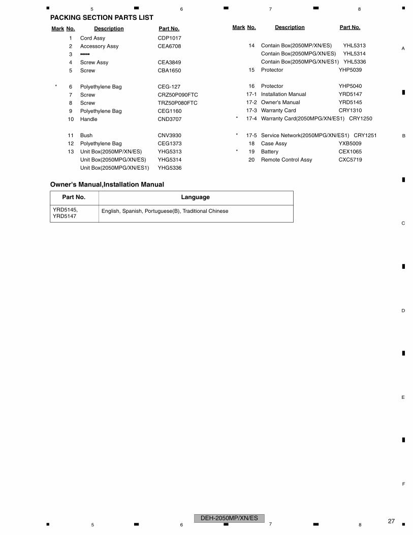
PACKING SECTION PARTS LIST
Owner's Manual,Installation Manual
Mark No. Description Part No.
1 Cord Assy CDP1017
2 Accessory Assy CEA6708
3 •••••
4 Screw Assy CEA3849
5 Screw CBA1650
* 6 Polyethylene Bag CEG-127
7 Screw CRZ50P090FTC
8 Screw TRZ50P080FTC
9 Polyethylene Bag CEG1160
10 Handle CND3707
11 Bush CNV3930
12 Polyethylene Bag CEG1373
13 Unit Box(2050MP/XN/ES) YHG5313
Unit Box(2050MPG/XN/ES) YHG5314
Unit Box(2050MPG/XN/ES1) YHG5336
14 Contain Box(2050MP/XN/ES) YHL5313
Contain Box(2050MPG/XN/ES) YHL5314
Contain Box(2050MPG/XN/ES1) YHL5336
15 Protector YHP5039
16 Protector YHP5040
17-1 Installation Manual YRD5147
17-2 Owner's Manual YRD5145
17-3 Warranty Card CRY1310
* 17-4 Warranty Card(2050MPG/XN/ES1) CRY1250
* 17-5 Service Network(2050MPG/XN/ES1) CRY1251
18 Case Assy YXB5009
* 19 Battery CEX1065
20 Remote Control Assy CXC5719
Mark No. Description Part No.
Part No. Language
YRD5145, YRD5147
English, Spanish, Portuguese(B), Traditional Chinese
DEH-2050MP/XN/ES 275 6 7 8

C
D
F
A
B
E
1 2 3 4
9.2 EXTERIOR
A
A
7
11
12
41
23 42
25 14
22
432218
20
29
24
21
28
40
17
15
1
1
1
1
404
26
27
39
37
33
34
10
35
8
9
3
2
38
32
36
31
30
A
5
16
13
66
67
B
44
45
55
56
57
46
49
51
6252
53 59
6563
6454
50
4858
60
61
48
47
DEH-2050MP/XN/ES281 2 3 4

C
D
F
A
B
E
5 6 7 8
EXTERIOR SECTION PARTS LIST
Mark No. Description Part No.
1 Screw BSZ26P060FTC
2 Screw BSZ26P100FTC
3 Screw BSZ26P180FTC
4 Cable CDE8336
5 Cord Assy CDP1017
6 •••••
7 Case CNB2793
8 Holder CND3598
9 Insulator CNN23255
10 Panel YNS5276
11 Tuner Amp Unit YWM5234
12 Screw BSZ26P060FTC
13 Screw BPZ26P080FTC
14 Screw BSZ26P160FTC
> 15 Fuse(10 A) YEK5001
16 Pin Jack(CN351) CKB1059
17 Plug(CN901) CKM1376
18 Connector(CN651) CKS3829
19 •••••
20 Connector(CN831) CKS5664
21 Antenna Jack(CN401) CKX1056
22 Holder CND3545
23 Holder CND3754
24 Holder CND3706
25 Heat Sink CNR1668
26 FM/AM Tuner Unit CWE2025
27 Holder CND3466
28 Terminal(CN402) VNF1084
29 Terminal(CN601) VNF1084
30 Button(DETACH) CAC4836
31 Spring CBH2367
32 Spring CBH2961
33 Spring CBH2962
34 Cover CNN1665
35 Panel CNS9206
36 Arm CNV9311
37 Arm CNV9312
38 Chassis Unit CXC7391
39 CD Mechanism Module(S10.5) CXK5763
40 Screw ISS26P055FTC
41 Transistor(Q991) 2SD2396
42 IC(IC301) PAL007C
43 IC(IC911) BA4918-V12
44 Grille Assy(2050MP/XN/ES) YXA5374
Grille Assy(2050MPG/XN/ES) YXA5367
Grille Assy(2050MPG/XN/ES1) YXA5367
45 Grille Unit(2050MP/XN/ES) YXA5334
Grille Unit(2050MPG/XN/ES) YXA5336
Grille Unit(2050MPG/XN/ES1) YXA5336
46 Knob Unit YXC5072
47 Spring YBL5010
48 Screw BPZ20P100FTC
49 Spring CBH2210
50 Button(Detach) YAC5217
51 Button(EJECT) YAC5218
52 Button(1 - 6) YAC5219
53 Button(AUDIO,EQ) YAC5220
54 Button(FUNC,BAND) YAC5221
55 Button(DISP,CLK) YAC5222
56 Button(UP,<) YAC5234
57 Button(DOWN,>) YAC5235
58 Cover YNS5248
59 LCD(LCD1801) CAW1930
60 Connector(CN1801) CKS5663
61 Jack(CN1802) YKN5001
62 Holder YNC5045
63 Lighting Conductor YNV5108
64 Rubber Contact YNV5109
65 Connector YNV5166
66 Remote Control Assy CXC5719
67 Cover CNS7068
Mark No. Description Part No.
DEH-2050MP/XN/ES 295 6 7 8

C
D
F
A
B
E
1 2 3 4
9.3 CD MECHANISM MODULE
DEH-2050MP/XN/ES301 2 3 4

C
D
F
A
B
E
5 6 7 8
CD MECHANISM MODULE SECTION PARTS LIST
Mark No. Description Part No.
1 CD Core Unit(S10.5COMP2) CWX3514
2 Connector(CN101) CKS4182
3 Connector(CN701) CKS4808
4 Screw BMZ20P025FTC
5 Screw BSZ20P040FTC
6 Screw(M2 x 3) CBA1511
7 Screw(M2 x 4) CBA1835
8 Washer CBF1038
9 •••••
10 Spring CBH2609
11 Spring CBH2612
12 Spring CBH2614
13 Spring CBH2616
14 Spring CBH2617
15 Spring CBH2620
16 Spring CBH2855
17 Spring CBH2937
18 Spring CBH2735
19 Spring CBH2854
20 Spring CBH2642
21 Spring CBH2856
22 Spring CBH2857
23 Spring CBH2860
24 Spring CBH2861
25 Spring CBL1686
26 Arm CND1909
27 Frame CND2582
28 Bracket CND2583
29 Arm CND2584
30 Lever CND2585
31 Arm CND2586
32 Bracket CND2587
33 Arm CND2588
34 Lever CND2589
35 Holder CNV7201
36 Gear CNV7207
37 Gear CNV7208
38 Gear CNV7209
39 Gear CNV7210
40 Gear CNV7211
41 Gear CNV7212
42 Rack CNV7214
43 Arm CNV7216
44 Roller CNV7218
45 Gear CNV7219
46 Guide CNV7361
47 Gear CNV7595
48 Guide CNV7799
49 Arm CNV7805
50 Rack CNV8342
51 Roller CNV8343
52 Holder CNV8344
53 Arm CNV8345
54 Guide CNV8347
55 Arm CNV8348
56 Arm CNV8349
57 Arm CNV8350
58 Clamper CNV8365
59 Arm CNV8386
60 Guide CNV8396
61 Arm CNV8413
62 Collar CNV8938
63 Motor Unit(M2) CXC4026
64 Arm Unit CXC4027
65 Chassis Unit CXC4028
66 Gear Unit CXC4029
67 Frame Unit CXC4031
68 Motor Unit(M1) CXC7134
69 Screw Unit CXC6359
70 Screw JFZ20P020FTC
71 Screw JGZ17P022FTC
72 Washer YE20FTC
73 Pickup Unit(P10.5)(Service) CXX1942
74 Screw IMS26P030FTC
Mark No. Description Part No.
DEH-2050MP/XN/ES 315 6 7 8

C
D
F
A
B
E
1 2 3 4
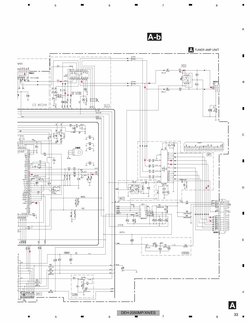
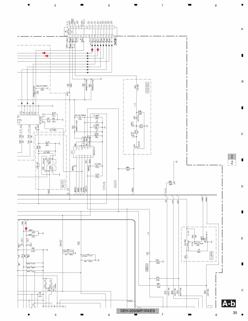
10. SCHEMATIC DIAGRAM10.1 OVERALL CONNECTION DIAGRAM(GUIDE PAGE)
A-a
A
A-a A-b
A-a A-b
A-bA-a
Large sizeSCH diagram
Guide page
Detailed page
Note: When ordering service parts, be sure to refer to " EXPLODED VIEWS AND PARTS LIST" or "ELECTRICAL PARTS LIST".
Decimal points for resistorand capacitor fixed valuesare expressed as :2.2 t 2R20.022 t R022
The > mark found on some component parts indicatesthe importance of the safety factor of the part.Therefore, when replacing, be sure to use parts ofidentical designation.
Symbol indicates a resistor.No differentiation is made between chip resistors anddiscrete resistors.
NOTE :
Symbol indicates a capacitor.No differentiation is made between chip capacitors anddiscrete capacitors.
BCN1801
C CN701
FM
/AM
TU
NE
R U
NIT
PDH131A
CD:+0.5dBs
DEH-2050MP/XN/ES321 2 3 4
C
D
F
A
B
E
N701
5 6 7 8
A-b
A
A TUNER AMP UNIT
>
B.UP
GND
B.REM
ACC
ANT
RL-
RL+
FL-
FL+
TEL
RR-
RR+
FR-
FR+1
2
3
4
5
6
7
8
9
10
11
12
13
14
15
16CEK1208>
10A
CD:+0.5dBs
FM:-14.33dBsAM: -25.5dBs
DEH-2050MP/XN/ES 335 6 7 8

C
D
F
A
B
E
1 2 3 4
A-a
A-b
A-b
AT
UN
ER
AM
P U
NIT
>
FM
:-14
.33d
Bs
AM
: -2
5.5d
Bs
DEH-2050MP/XN/ES341 2 3 4
C
D
F
A
B
E
5 6 7 8
A-a
A-b
A-b
B.U
P
GN
D
B.R
EM
AC
C
AN
T
RL-
RL+FL-
FL+
TE
L
RR
-
RR
+
FR
-
FR
+12345678910111213141516
CEK
1208
> 10A
DEH-2050MP/XN/ES 355 6 7 8

C
D
F
A
B
E
1 2 3 4
A-b
A-a
A-a
A-bC
CN
701
FM/AM TUNER UNIT
PD
H13
1A
CD
:+0.
5dB
s
DEH-2050MP/XN/ES361 2 3 4

C
D
F
A
B
E
5 6 7 8
A-a
A-b
A-b
A-a
Dec
imal
poi
nts
for
resi
stor
and
capa
cito
r fix
ed v
alue
sar
e ex
pres
sed
as :
2.2
t 2
R2
0.02
2t
R02
2
The
> m
ark
foun
d on
som
e co
mpo
nent
par
ts in
dica
tes
the
impo
rtan
ce o
f the
saf
ety
fact
or o
f the
par
t.T
here
fore
, whe
n re
plac
ing,
be
sure
to u
se p
arts
of
iden
tical
des
igna
tion.
Sym
bol i
ndic
ates
a r
esis
tor.
No
diffe
rent
iatio
n is
mad
e b
etw
een
chip
res
isto
rs a
nddi
scre
te r
esis
tors
.
NO
TE
: Sym
bol i
ndic
ates
a c
apac
itor.
No
diffe
rent
iatio
n is
mad
e b
etw
een
chip
cap
acito
rs a
nddi
scre
te c
apac
itors
.
BC
N18
01
DEH-2050MP/XN/ES 375 6 7 8

C
D
F
A
B
E
D1821
R1805
1807
1 2 3 4
10.2 KEYBOARD UNIT
B
1
GP1UX51RK
100
2R2
10 10K
D1803-
R1803-
R1806,R
DEH-2050MP/XN/ES381 2 3 4

C
D
F
A
B
E
D18
R18
R18
5 6 7 8
B
4700
P47
00P
47K
2R2K
2R2K
100
100
820
YS
D50
18
CL-195SR-CD(SUPER RED)
CL-195PG-CD(PURE GREEN)03-D1821
2050MP/XN/ES2050MPG/XN/ES2050MPG/XN/ES1
03-R1805 820 680
06,R1807 680 470
CLK
ACN831
B KEYBOARD UNIT
DEH-2050MP/XN/ES 395 6 7 8

C
D
F
A
B
E
1 2 3 4
10.3 CD MECHANISM MODULE(GUIDE PAGE)
C-a
C
M1 CXC7134SPINDLE MOTOR
M2 CXC4026LOADING/CARRIAGE MOTOR
PICKUP UNIT(P10.5)(SERVICE)
SWITCHES:CD CORE UNIT(S10.5COMP2) S901:HOME SWITCH..........ON-OFF S903:DSCSNS SWITCH......ON-OFF S904:12EJ SWITCH.............ON-OFF S905:8EJ SWITCH...............ON-OFF
The underlined indicates the switch position.
CD DRIVER
F
F
T
T
F
F
T
TF
F
T
T
F
F
T
T
F
T
S
C
C
S
S
C
3
2
1
9
0 48
7
$
5
@
#
%
DEH-2050MP/XN/ES401 2 3 4

C
D
F
A
B
E
5 6 7 8
C-b
C
C CD CORE UNIT(S10.5COMP2)
ACN651
FSIGNAL LINE
FOCUS SERVO LINE
TRACKING SERVO LINE
CARRIAGE SERVO LINE
SPINDLE SERVO LINE
T
C
S
!
6
&^
DEH-2050MP/XN/ES 415 6 7 8

C
D
F
A
B
E
1 2 3 4
C-a
C-b
C-b 1
CC
D C
OR
E U
NIT
(S10
.5C
OM
P2)
FS
IGN
AL
LIN
E
FO
CU
S S
ER
VO
LIN
E
TR
AC
KIN
G S
ER
VO
LIN
E
CA
RR
IAG
E S
ER
VO
LIN
E
SP
IND
LE S
ER
VO
LIN
E
T C S
!
DEH-2050MP/XN/ES421 2 3 4

C
D
F
A
B
E
5 6 7 8
C-a
C-b
C-b2 3
AC
N65
1
6
&^
DEH-2050MP/XN/ES 435 6 7 8

C
D
F
A
B
E
S
903:
DS
CS
NS
SW
ITC
H...
...O
N-O
FF
S
904:
12E
J S
WIT
CH
......
......
.ON
-OF
F
S90
5:8E
J S
WIT
CH
......
......
...O
N-O
FF
1 2 3 4
C-b
C-a
C-a
C-b 1
PIC
KU
P U
NIT
(P10
.5)(
SE
RV
ICE
)
SW
ITC
HE
S:
CD
CO
RE
UN
IT(S
10.5
CO
MP
2)
S90
1:H
OM
E S
WIT
CH
......
....O
N-O
FF
F F TT
FF T TFF T T
FF T T
@#
%
DEH-2050MP/XN/ES441 2 3 4

C
D
F
A
B
E
5 6 7 8
C-a
C-b
c-b
C-a
2 3
M1
CX
C71
34S
PIN
DLE
MO
TO
R
M2
CX
C40
26LO
AD
ING
/CA
RR
IAG
E M
OT
OR
SW
ITC
HE
S:
CD
CO
RE
UN
IT(S
10.5
CO
MP
2)
S90
1:H
OM
E S
WIT
CH
......
....O
N-O
FF
S
903:
DS
CS
NS
SW
ITC
H...
...O
N-O
FF
S
904:
12E
J S
WIT
CH
......
......
.ON
-OF
F
S90
5:8E
J S
WIT
CH
......
......
...O
N-O
FF
The
und
erlin
ed in
dica
tes
the
switc
h po
sitio
n.
CD
DR
IVE
R
FT
S C CS
S
C
3 2 1
9 04
87
$
5
DEH-2050MP/XN/ES 455 6 7 8

C
D
F
A
B
E
1 2 3 4
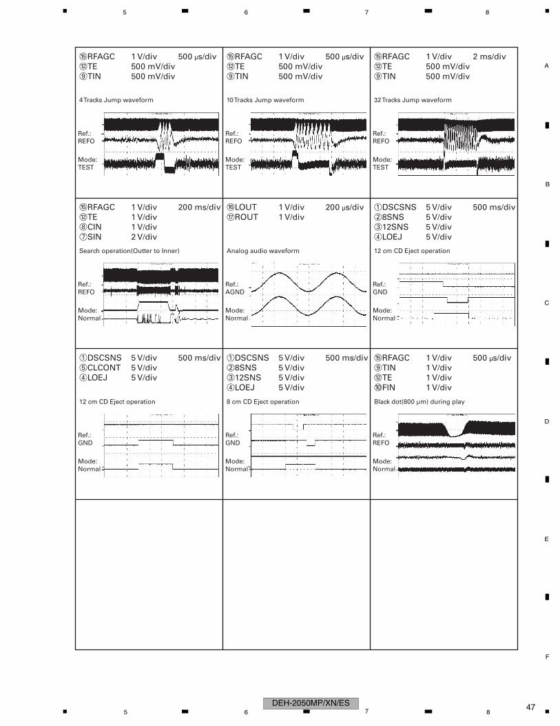
10.4 WAVEFORMS
- CD Core Unit Note : 1. The encircled numbers denote measuring points in the circuit diagram.2. Reference voltage REFO1(1.65 V)
500 ms/div5 V/div5 V/div5 V/div10 V/div
1DSCSNS5CLCONT4LOEJ6VD
5 V/div5 V/div5 V/div5 V/div
1DSCSNS28SNS312SNS4LOEJ
5 V/div5 V/div5 V/div5 V/div
500 ms/div1DSCSNS28SNS312SNS4LOEJ
500 mV/div500 mV/div
200 ms/div@TE#FE
200 mV/div2 V/div2 V/div
500 ms/div0FIN!RFOK(MONI_2)7SIN
1 V/div500 mV/div1 V/div
1 s/div
500 ms/div
7SIN8CIN9TIN
2 V/div500 mV/div
5 µs/div$MDX7SIN
2 V/div500 mV/div
200 ms/div$MDX7SIN
500 mV/div500 mV/div500 mV/div500 mV/div
20 ms/div#FE0FIN@TE9TIN
1 V/div500 mV/div500 mV/div
500 µs/div%RFAGC@TE9TIN
500 mV/div500 mV/div
2 ms/div@TE%RFAGC
500 mV/div500 mV/div
200 ms/div0FIN#FE
Source On setup operation12 cm CD-DA Source On setup operation
CD-DA Play operation Spindle waveform during play operation Spindle waveform during play operation(Wider)
Focus Search waveform Track Open waveform 1 Track Jump waveform
12 cm CD-DA setup operation after loading
12 cm CD Loading operation 12 cm CD Loading operation 8 cm CD Loading operation
Ref.:GND
Mode:Normal
Ref.:GND
Mode:Normal
Ref.:GND
Mode:Normal
Ref.:REFO
Mode:Normal
Ref.:REFO
Mode:Normal
Ref.:REFO
Mode:Normal
Ref.:REFO
Mode:TEST
Ref.:REFO
Mode:TEST
Ref.:REFO
Mode:TEST
Ref.:REFO
Mode:Normal
Ref.:REFO
Mode:Normal
Ref.:REFO
Mode:Normal
DEH-2050MP/XN/ES461 2 3 4
C
D
F
A
B
E
5 6 7 8
1 V/div500 mV/div500 mV/div
2 ms/div%RFAGC@TE9TIN
1 V/div500 mV/div500 mV/div
500 µs/div%RFAGC@TE9TIN
1 V/div500 mV/div500 mV/div
500 µs/div%RFAGC@TE9TIN
5 V/div5 V/div5 V/div5 V/div
500 ms/div1DSCSNS28SNS312SNS4LOEJ
1 V/div1 V/div
200 µs/div^LOUT&ROUT
1 V/div1 V/div1 V/div2 V/div
200 ms/div%RFAGC@TE8CIN7SIN
1 V/div1 V/div1 V/div1 V/div
500 µs/div%RFAGC9TIN@TE0FIN
5 V/div5 V/div5 V/div5 V/div
500 ms/div1DSCSNS28SNS312SNS4LOEJ
5 V/div5 V/div5 V/div
500 ms/div1DSCSNS5CLCONT4LOEJ
12 cm CD Eject operationAnalog audio waveform
12 cm CD Eject operation 8 cm CD Eject operation Black dot(800 µm) during play
Search operation(Outter to Inner)
4 Tracks Jump waveform 10 Tracks Jump waveform 32 Tracks Jump waveform
Ref.:REFO
Mode:TEST
Ref.:REFO
Mode:TEST
Ref.:REFO
Mode:TEST
Ref.:GND
Mode:Normal
Ref.:REFO
Mode:Normal
Ref.:GND
Mode:Normal
Ref.:REFO
Mode:Normal
Ref.:GND
Mode:Normal
Ref.:AGND
Mode:Normal
DEH-2050MP/XN/ES 475 6 7 8

C
D
F
A
B
E
1 2 3 4
11. PCB CONNECTION DIAGRAM11.1 TUNER AMP UNIT
A
A TUNER AMP UNIT
CapacitorConnector
P.C.Board Chip PartSIDE B
SIDE A
NOTE FOR PCB DIAGRAMS1.The parts mounted on this PCB include all necessary parts for several destination. For further information for respective destinations, be sure to check with the schematic dia- gram.2.Viewpoint of PCB diagrams
C CN701
B CN1801
CORD ASSY
DEH-2050MP/XN/ES481 2 3 4

C
D
F
A
B
E
ASSY
5 6 7 8
A
SIDE A
FRONT
FM
/AM
TU
NE
R U
NIT
ANTENNA
RCA OUTPUT
DEH-2050MP/XN/ES 495 6 7 8

C
D
F
A
B
E
1 2 3 4
A
A TUNER AMP UNIT
TESTIN
SCET
DEH-2050MP/XN/ES501 2 3 4

C
D
F
A
B
E
5 6 7 8
A
SIDE B
DEH-2050MP/XN/ES 515 6 7 8

C
D
F
A
B
E
1 2 3 4
11.2 KEYBOARD UNIT
B
SIDE AB KEYBOARD UNIT
CLK
DIS
P
FU
NC
SO
UR
CE
/VO
L
AU
DIO
EQ
12
34
56E
JEC
T
BA
ND
DEH-2050MP/XN/ES521 2 3 4

C
D
F
A
B
E
5 6 7 8
B
SIDE BB KEYBOARD UNIT
ACN831
DEH-2050MP/XN/ES 535 6 7 8

C
D
F
A
B
E
1 2 3 4
11.3 CD CORE UNIT(S10.5COMP2)
C
SIDE AC CD CORE UNIT(S10.5COMP2)
PICKUP UNIT(P10.5)(SERVICE)A CN651
M2LOADING
/CARRIAGEMOTOR
M1SPINDLEMOTOR
DEH-2050MP/XN/ES541 2 3 4

C
D
F
A
B
E
5 6 7 8
C
SIDE BC CD CORE UNIT(S10.5COMP2)
DEH-2050MP/XN/ES 555 6 7 8

C
D
F
A
B
E
1 2 3 4
12. ELECTRICAL PARTS LIST
NOTE: Parts whose parts numbers are omitted are subject to being not supplied. The part numbers shown below indicate chip components. Chip Resistor RS1/_S___J,RS1/__S___J Chip Capacitor (except for CQS.....) CKS....., CCS....., CSZS..... The > mark found on some component parts indicates the importance of the safety factor of the part. Therefore, when replacing, be sure to use parts of identical designation. Meaning of the figures and others in the parentheses in the parts list. Example) IC 301 is on the point (face A, 91 of x-axis, and 111 of y-axis) of the corresponding PC board. IC 301 (A, 91, 111) IC NJM2068V
Circuit Symbol and No. Part No.
Unit Number : YWM5234
Unit Name : Tuner Amp Unit
Unit Number : (2050MP/XN/ES)
Unit Name : Keyboard Unit
Unit Number : (2050MPG/XN/ES)
Unit Number : (2050MPG/XN/ES1)
Unit Name : Keyboard Unit
Unit Number : CWX3514
Unit Name : CD Core
Unit(S10.5COMP2)
AUnit Number : YWM5234Unit Name : Tuner Amp Unit
MISCELLANEOUS
IC 151 (B,124,101) IC PML014AIC 301 (A,95,133) IC PAL007CIC 601 (B,129,44) IC PN5013BIC 641 (B,161,30) IC PDH131AIC 911 (A,17,68) IC BA4918-V12Q 201 (B,130,130) Transistor RT3T22M
Q 351 (B,162,127) Transistor RT3N66MQ 601 (A,152,67) Transistor 2SD1858Q 821 (B,32,12) Transistor 2SA1036KQ 822 (B,23,11) Transistor RT1N141M-11Q 931 (B,59,97) Transistor 2SC2412K
Q 991 (A,8,115) Transistor 2SD2396Q 992 (B,14,106) Transistor RT3T22MD 301 (A,67,124) Diode MPG06G-6415G3D 302 (A,54,124) Diode MPG06G-6415G3D 832 (B,75,8) Diode FTZ6R8E
D 901 (A,49,110) Diode MPG06G-6415G3D 902 (A,49,107) Diode MPG06G-6415G3
D 911 (A,52,80) Diode MPG06G-6415G3D 912 (A,45,80) Diode MPG06G-6415G3D 931 (A,65,109) Diode HZS7L(A1)
D 991 (A,20,113) Diode HZS7L(C3)L 151 (A,138,106) Inductor LAU2R2KL 401 (A,150,82) Inductor LAU2R2KL 402 (A,146,98) Inductor LAU2R2KL 407 (B,166,66) Inductor CTF1473
L 601 (B,119,22) Inductor CTF1389L 602 (A,152,25) Inductor LAUR47KL 603 (A,113,79) Inductor LAU2R2KL 604 (A,122,70) Inductor LAUR47KL 605 (A,128,69) Inductor LAUR47K
L 606 (A,147,69) Inductor LAU1R0KL 607 (A,148,61) Inductor LAU1R0KL 608 (A,135,69) Inductor LAU1R5KL 609 (A,133,69) Inductor LAU1R5KL 610 (A,140,67) Inductor LAU1R2J
L 611 (B,137,82) Inductor CTF1379L 612 (B,135,82) Inductor CTF1379L 613 (B,145,61) Inductor CTF1379L 614 (B,123,67) Inductor CTF1379L 615 (B,153,73) Inductor CTF1379
L 616 (B,145,77) Inductor CTF1379L 617 (B,147,52) Inductor CTF1389L 801 (A,73,24) Inductor LAU2R2KL 901 (A,36,98) Choke Coil 600 µH CTH1280X 601 (A,142,62) Oscillator 74.100 MHz CSS1749
X 602 (A,115,58) Oscillator 4.7186 MHz CSS1727>FU351 (B,135,132) Fuse 3 A CEK1286AR401 (B,164,111) Surge Protector IMSA-6801-01Y901
(A,165,75) FM/AM Tuner Unit CWE2025
RESISTORS
R 151 (B,89,95) RAB4C102JR 156 (B,91,88) RS1/16S681JR 157 (B,94,88) RS1/16S681JR 162 (B,139,101) RS1/16S102JR 163 (B,106,106) RS1/16S102J
R 201 (B,125,130) RS1/16S103JR 202 (B,132,134) RS1/16S153J
Circuit Symbol and No. Part No.
DEH-2050MP/XN/ES561 2 3 4

C
D
F
A
B
E
5 6 7 8
R 203 (B,125,131) RS1/16S221JR 251 (B,104,106) RS1/16S223JR 252 (B,137,101) RS1/16S223J
R 301 (B,95,107) RS1/16S153JR 351 (B,166,131) RS1/16S223JR 352 (B,166,135) RS1/16S223JR 353 (B,147,118) RS1/16S821JR 354 (B,165,126) RS1/16S821J
R 404 (B,157,44) RS1/16S102JR 405 (B,161,54) RS1/16S102JR 406 (B,161,60) RS1/16S102JR 407 (B,161,62) RS1/16S102JR 408 (B,169,50) RAB4C104J
R 409 (B,161,47) RS1/16S391JR 410 (B,161,49) RS1/16S681JR 411 (B,161,51) RS1/16S681JR 412 (B,161,53) RS1/16S681JR 413 (B,161,56) RS1/16S472J
R 601 (B,125,28) RS1/16S473JR 603 (B,108,40) RS1/16S473JR 606 (B,109,70) RS1/16S473JR 608 (B,141,60) RS1/16S470JR 610 (B,123,64) RS1/16S203J
R 611 (B,139,71) RS1/16S182JR 612 (B,117,75) RS1/16S563JR 613 (B,142,52) RS1/16S302JR 615 (B,114,75) RS1/16S563JR 616 (B,159,40) RS1/16S104J
R 617 (B,137,32) RS1/16S473JR 618 (B,148,41) RS1/16S473JR 619 (B,149,39) RS1/16S104JR 638 (B,160,88) RS1/16S273JR 641 (B,153,37) RS1/16S103JR 642 (B,151,33) RS1/16S103J
R 643 (B,159,38) RS1/16S104JR 644 (B,99,67) RS1/16S0R0JR 645 (B,101,19) RS1/16S0R0JR 646 (B,160,16) RS1/16S0R0JR 648 (B,159,74) RS1/16S0R0JR 651 (B,34,30) RS1/16S104J
R 652 (B,34,35) RS1/16S102JR 653 (B,34,34) RS1/16S102JR 654 (B,34,32) RS1/16S221JR 656 (B,107,26) RS1/16S104JR 657 (B,107,28) RS1/16S104J
R 658 (B,34,37) RS1/16S104JR 659 (B,107,30) RS1/16S472JR 660 (B,107,32) RS1/16S472JR 661 (B,111,28) RS1/16S221JR 662 (B,111,30) RS1/16S221J
R 663 (B,111,32) RS1/16S221JR 664 (B,79,54) RS1/16S473JR 666 (B,168,30) RS1/16S103JR 671 (B,136,24) RS1/16S473JR 672 (B,110,46) RS1/16S104J
R 673 (B,137,27) RAB4C104JR 674 (B,132,27) RS1/16S104JR 675 (B,94,59) RS1/16S473JR 677 (B,122,22) RS1/16S104JR 803 (B,86,18) RS1/16S222J
Circuit Symbol and No. Part No.R 821 (B,27,13) RS1/16S562JR 822 (B,27,11) RS1/16S103JR 831 (B,36,12) RS1/16S1R0JR 832 (B,86,26) RS1/16S473JR 833 (A,81,23) RD1/4PU222J
R 834 (A,83,23) RD1/4PU222JR 835 (A,62,21) RD1/4PU222JR 837 (A,77,19) RD1/4PU103JR 839 (A,89,14) RD1/4PU222JR 840 (A,86,14) RD1/4PU222J
R 841 (B,75,27) RS1/16S104JR 855 (B,81,67) RS1/16S104JR 873 (B,140,24) RS1/16S103JR 874 (B,140,31) RS1/16S103JR 931 (B,106,40) RS1/16S104J
R 932 (B,62,100) RS1/16S223JR 933 (A,70,106) RD1/4PU102JR 934 (B,67,113) RS1/16S472JR 935 (B,62,115) RS1/16S473JR 991 (A,14,116) RD1/4PU271J
CAPACITORS
C 151 (B,109,101) CKSRYB224K10C 152 (B,133,95) CKSRYB224K10C 153 (B,109,104) CKSRYB105K10C 154 (B,133,98) CKSRYB105K10C 155 (A,126,113) CEJQ470M10
C 156 (B,134,101) CKSRYB105K10C 157 (B,109,106) CKSRYB105K10C 162 (B,134,103) CKSRYB105K10C 163 (B,109,108) CKSRYB105K10C 164 (A,120,113) CEJQ100M16
C 165 (B,123,112) CKSRYB104K16C 201 (A,129,134) CEJQ330M10C 253 (B,97,104) CKSRYB104K16C 301 (B,126,122) CKSQYB474K16C 302 (B,122,122) CKSQYB474K16
C 303 (B,124,122) CKSQYB474K16C 304 (B,120,122) CKSQYB474K16C 305 (B,126,126) CKSRYB474K10C 306 (B,122,126) CKSRYB474K10C 307 (B,124,126) CKSRYB474K10
C 308 (B,120,126) CKSRYB474K10C 309 (B,124,139) CKSQYB225K10C 310 (B,116,144) CKSQYB225K10C 312 (A,101,122) CEJQ100M16C 313 (B,101,141) CKSRYB104K16
C 353 (A,145,119) CEJQ2R2M50C 354 (A,143,112) CEJQ2R2M50C 359 (B,164,137) CCSQCH471J50C 402 (B,142,100) CKSRYB103K50C 404 (A,150,97) CEJQ101M10
C 405 (B,146,100) CKSRYB103K50C 406 (B,169,53) CCSRCH390J50C 409 (B,161,45) CCSRCH100D50C 601 (B,120,27) CKSRYB105K10C 602 (B,121,30) CKSRYB103K50
C 603 (B,123,28) CKSRYB103K50C 605 (B,108,74) CKSRYB104K16
Circuit Symbol and No. Part No.
DEH-2050MP/XN/ES 575 6 7 8

C
D
F
A
B
E
1 2 3 4
C 606 (B,105,56) CKSRYB103K50C 607 (B,118,55) CKSRYB103K50C 608 (B,95,80) CKSRYB103K50
C 609 (B,116,72) CKSRYB331K50C 610 (A,98,80) CEJQ101M6R3C 611 (B,116,70) CKSRYB331K50C 612 (B,120,58) CKSRYB103K50C 613 (A,104,58) CEAL101M6R3
C 614 (B,168,88) CKSRYB102K50C 615 (B,125,62) CKSRYB331K50C 616 (B,125,69) CKSRYB105K10C 617 (B,130,61) CKSRYB105K10C 618 (B,113,54) CCSRCH270J50
C 619 (B,144,71) CKSRYB103K50C 620 (B,144,57) CKSRYB105K10C 621 (B,152,70) CKSRYB103K50C 622 (B,142,54) CKSRYB104K16C 623 (B,134,66) CKSRYB102K50
C 624 (B,131,66) CKSRYB102K50C 625 (B,137,72) CCSRCH270J50C 626 (B,131,72) CCSRCH270J50C 627 (B,136,79) CCSRCH150J50C 628 (B,143,64) CKSRYB102K50
C 629 (B,136,60) CCSRCH4R0C50C 630 (B,144,69) CCSRCH8R0D50C 631 (B,108,72) CKSRYB223K50C 632 (B,130,23) CKSRYB104K16C 633 (B,147,31) CKSRYB104K16
C 634 (B,113,58) CCSRCH270J50C 635 (B,147,55) CKSRYB104K16C 637 (B,110,77) CKSRYB103K50C 640 (B,125,60) CKSRYB104K16C 642 (B,109,103) CKSRYB182K50
C 643 (B,133,99) CKSRYB182K50C 646 (B,116,22) CKSRYB103K50C 652 (B,49,31) CKSRYB103K50C 653 (B,114,33) CCSRCH220J50C 821 (B,36,10) CKSRYB104K16
C 825 (B,61,8) CCSRCH221J50C 826 (B,82,14) CCSRCH221J50C 827 (B,71,8) CCSRCH221J50C 828 (B,69,8) CCSRCH221J50C 829 (B,63,8) CCSRCH221J50
C 830 (B,65,8) CKSRYB104K16C 831 (B,67,8) CCSRCH221J50C 901 (A,52,114) 3 300 µF/16 V CCH1732C 911 (A,59,62) CEJQ100M16C 912 (A,48,66) CEAT102M16
C 913 (B,28,71) CKSRYB104K16C 914 (A,52,62) CEAT221M10C 915 (A,46,55) CEJQ100M16C 916 (A,58,55) 1 000 µF/6.3 V CCH1751(P35)C 917 (B,28,77) CKSRYB104K16
C 991 (B,11,108) CKSRYB473K25C 992 (A,12,97) CEJQ101M10
BUnit Number : (2050MP/XN/ES)Unit Name : Keyboard Unit
Circuit Symbol and No. Part No.
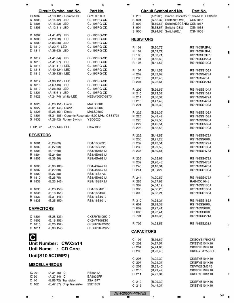
MISCELLANEOUS
IC 1801 (B,26,121) IC PD6340AIC 1802 (A,10,161) Remote IC GP1UX51RKD 1803 (A,14,42) LED CL-195SR-CDD 1805 (A,15,23) LED CL-195SR-CDD 1806 (A,12,11) LED CL-195SR-CD
D 1807 (A,41,42) LED CL-195SR-CDD 1808 (A,28,28) LED CL-195SR-CDD 1809 (A,35,20) LED CL-195SR-CDD 1810 (A,22,7) LED CL-195SR-CDD 1811 (A,36,63) LED CL-195SR-CD
D 1812 (A,41,84) LED CL-195SR-CDD 1813 (A,41,97) LED CL-195SR-CDD 1814 (A,41,111) LED CL-195SR-CDD 1815 (A,40,124) LED CL-195SR-CDD 1816 (A,39,138) LED CL-195SR-CD
D 1817 (A,38,151) LED CL-195SR-CDD 1818 (A,6,149) LED CL-195SR-CDD 1819 (A,28,55) LED CL-195SR-CDD 1821 (A,15,61) LED CL-195SR-CDD 1822 (A,24,74) White LED NESW505C-5273
D 1826 (B,26,151) Diode MALS068XD 1827 (B,31,148) Diode MALS068XD 1828 (B,28,151) Diode MALS068XX 1801 (B,31,106) Ceramic Resonator 5.00 MHz CSS1731S 1833 (A,28,42) Rotary Switch YSD5018
LCD1801 (A,15,149) LCD CAW1930
RESISTORS
R 1801 (B,29,89) RS1/16S222JR 1802 (B,27,93) RS1/16S222JR 1803 (B,19,68) RS1/4SA821JR 1804 (B,24,68) RS1/4SA821JR 1805 (B,36,96) RS1/4SA821J
R 1806 (B,36,100) RS1/4SA681JR 1807 (B,22,68) RS1/4SA681JR 1809 (B,27,50) RS1/16S473JR 1810 (B,26,75) RS1/4SA821JR 1833 (B,23,145) RS1/16S2R2J
R 1835 (B,23,150) RS1/16S101JR 1836 (B,18,154) RS1/16S103JR 1837 (B,31,146) RS1/16S101JR 1838 (B,25,150) RS1/16S101J
CAPACITORS
C 1801 (B,28,133) CKSRYB105K10C 1803 (B,18,152) CKSYF106Z10C 1810 (B,23,152) CKSRYB472K50C 1811 (B,30,152) CKSRYB472K50
BUnit Number : (2050MPG/XN/ES)Unit Number : (2050MPG/XN/ES1)Unit Name : Keyboard Unit
MISCELLANEOUS
IC 1801 (B,26,121) IC PD6340A
Circuit Symbol and No. Part No.
DEH-2050MP/XN/ES581 2 3 4
C
D
F
A
B
E
5 6 7 8
IC 1802 (A,10,161) Remote IC GP1UX51RKD 1803 (A,14,42) LED CL-195PG-CDD 1805 (A,15,23) LED CL-195PG-CDD 1806 (A,12,11) LED CL-195PG-CD
D 1807 (A,41,42) LED CL-195PG-CDD 1808 (A,28,28) LED CL-195PG-CDD 1809 (A,35,20) LED CL-195PG-CDD 1810 (A,22,7) LED CL-195PG-CDD 1811 (A,36,63) LED CL-195PG-CD
D 1812 (A,41,84) LED CL-195PG-CDD 1813 (A,41,97) LED CL-195PG-CDD 1814 (A,41,111) LED CL-195PG-CDD 1815 (A,40,124) LED CL-195PG-CDD 1816 (A,39,138) LED CL-195PG-CD
D 1817 (A,38,151) LED CL-195PG-CDD 1818 (A,6,149) LED CL-195PG-CDD 1819 (A,28,55) LED CL-195PG-CDD 1821 (A,15,61) LED CL-195PG-CDD 1822 (A,24,74) White LED NESW505C-5273
D 1826 (B,26,151) Diode MALS068XD 1827 (B,31,148) Diode MALS068XD 1828 (B,28,151) Diode MALS068XX 1801 (B,31,106) Ceramic Resonator 5.00 MHz CSS1731S 1833 (A,28,42) Rotary Switch YSD5020
LCD1801 (A,15,149) LCD CAW1930
RESISTORS
R 1801 (B,29,89) RS1/16S222JR 1802 (B,27,93) RS1/16S222JR 1803 (B,19,68) RS1/4SA681JR 1804 (B,24,68) RS1/4SA681JR 1805 (B,36,96) RS1/4SA681J
R 1806 (B,36,100) RS1/4SA471JR 1807 (B,22,68) RS1/4SA471JR 1809 (B,27,50) RS1/16S473JR 1810 (B,26,75) RS1/4SA821JR 1833 (B,23,145) RS1/16S2R2J
R 1835 (B,23,150) RS1/16S101JR 1836 (B,18,154) RS1/16S103JR 1837 (B,31,146) RS1/16S101JR 1838 (B,25,150) RS1/16S101J
CAPACITORS
C 1801 (B,28,133) CKSRYB105K10C 1803 (B,18,152) CKSYF106Z10C 1810 (B,23,152) CKSRYB472K50C 1811 (B,30,152) CKSRYB472K50
CUnit Number : CWX3514Unit Name : CD Core
Unit(S10.5COMP2)
MISCELLANEOUS
IC 201 (A,34,46) IC PE5547AIC 301 (A,27,14) IC BA5839FPQ 101 (B,56,72) Transistor 2SA1577Q 102 (B,47,57) Chip Transistor 2SB1689
Circuit Symbol and No. Part No.X 201 (A,23,35) Ceramic Resonator 16.934 MHz CSS1603S 901 (A,53,37) Switch(HOME) CSN1067S 903 (B,19,58) Switch(DSCSNS) CSN1067S 904 (B,38,67) Switch(12EJ) CSN1068S 905 (B,24,68) Switch(8EJ) CSN1068
RESISTORS
R 101 (B,60,73) RS1/10SR2R4JR 102 (B,59,71) RS1/10SR2R4JR 103 (B,60,71) RS1/10SR2R7JR 104 (B,52,69) RS1/16SS222JR 105 (B,41,57) RS1/16SS102J
R 107 (B,41,59) RS1/16SS105JR 202 (B,32,62) RS1/16SS473JR 203 (B,42,45) RS1/16S473JR 204 (A,25,61) RS1/16SS221J
R 206 (B,26,53) RS1/16SS104JR 210 (B,13,32) RS1/16SS102JR 214 (B,36,34) RS1/16SS472JR 216 (B,47,49) RS1/16SS472JR 221 (B,36,32) RS1/16SS103J
R 222 (B,35,32) RS1/16SS103JR 225 (A,49,49) RS1/16SS103JR 226 (A,49,50) RS1/16SS393JR 227 (B,45,51) RS1/16SS562JR 228 (B,42,53) RS1/16SS122J
R 229 (B,44,53) RS1/16SS472JR 230 (B,21,28) RS1/16SS0R0JR 232 (B,43,51) RS1/16SS122JR 233 (B,29,52) RS1/16SS103JR 234 (B,30,61) RS1/16SS473J
R 235 (A,25,63) RS1/16SS473JR 239 (B,26,48) RS1/16SS473JR 240 (B,10,31) RS1/16SS473JR 241 (B,9,32) RS1/16SS103J
R 244 (A,20,52) RS1/16SS473JR 255 (A,27,63) RAB4CQ104JR 307 (A,34,19) RS1/16SS183JR 308 (A,38,20) RS1/16SS183JR 309 (A,35,21) RS1/16SS183J
R 310 (A,38,21) RS1/16SS183JR 601 (B,28,38) RS1/16SS0R0JR 602 (B,27,41) RS1/16SS0R0JR 606 (B,23,41) RS1/16SS0R0JR 701 (B,16,35) RS1/16SS221J
R 702 (A,23,55) RS1/16SS221J
CAPACITORS
C 106 (B,56,69) CKSQYB475K6R3C 202 (A,27,57) CKSSYB104K10C 204 (A,24,63) CKSSYB103K16C 205 (B,23,43) CKSQYB475K6R3
C 206 (A,22,39) CKSSYB104K10C 207 (A,24,37) CKSRYB104K16C 209 (B,33,40) CEVW220M6R3C 210 (B,29,42) CKSSYB104K10C 211 (A,27,34) CKSSYB104K10
C 212 (B,29,32) CKSRYB104K16C 213 (A,44,37) CKSSYB104K10
Circuit Symbol and No. Part No.
DEH-2050MP/XN/ES 595 6 7 8

C
D
F
A
B
E
1 2 3 4
C 214 (A,28,33) CKSSYB104K10C 216 (A,50,51) CKSSYB332K50C 217 (A,46,51) CKSSYB104K10
C 218 (A,49,51) CKSSYB473K10C 219 (A,45,53) CKSSYB104K10C 220 (A,46,53) CKSSYB182K50C 221 (A,44,53) CKSSYB104K10C 222 (B,43,53) CCSSCH560J50
C 223 (B,45,53) CCSSCH4R0C50C 224 (A,43,55) CKSSYB104K10C 226 (A,40,58) CCSSCH680J50C 227 (A,40,60) CCSSCH470J50C 228 (A,39,62) CKSSYB103K16
C 229 (B,49,59) CKSSYB104K10C 236 (A,42,61) CKSSYB104K10C 239 (B,44,51) CCSSCH220J50C 240 (A,35,61) CKSSYB104K10C 250 (B,36,30) CKSSYB102K50
C 251 (B,33,29) CKSSYB102K50C 303 (A,35,19) CKSSYB472K25C 304 (A,34,21) CKSSYB223K16C 307 (B,25,9) CKSRYB104K16C 308 (B,10,27) CKSRYB105K10
C 703 (B,11,37) CCSSCH101J50C 704 (B,8,36) CKSSYB102K50C 711 (A,25,26) CKSSYB104K10
Miscellaneous Parts List
Pickup Unit(P10.5)(Service) CXX1942M 1 Motor Unit(SPINDLE) CXC7134M 2 Motor Unit(LOADING/CARRIAGE) CXC4026
Circuit Symbol and No. Part No.
DEH-2050MP/XN/ES601 2 3 4