Piezoelectric Nanogenerators Based on Zno Nanostructures (1)

Piezoelectric Transformer Characterizationand
Application of Electronic Ballast
Ray-Lee Lin
Dissertation submitted to the Faculty of the
Virginia Polytechnic Institute and State University
in partial fulfillment of the requirement for the degree of
Doctor of Philosophy
in
Electrical Engineering
Fred C. Lee, Chair
Dusan Borojevic
Dan Y. Chen
Guo-Quan Lu
Douglas J. Nelson
Jacobus D. Van Wyk
November 26, 2001
Blacksburg, Virginia
Keywords: inductor-less, ZVS, PFC, equivalent circuit, model
Copyright 2001, Ray-Lee Lin

Dedicated to Jia-Bin (Robin) Chen
A deceased former graduate student/research assistant
Piezoelectric Transformer Research Group
VPEC/CPES, Virginia Tech

Piezoelectric Transformer Characterizationand
Application of Electronic Ballast
by
Ray-Lee Lin
Fred C. Lee, Chair
Electrical and Computer Engineering
(ABSTRACT)
The characterization and modeling of piezoelectric transformers are studied and
developed for use in electronic ballasts. By replacing conventional L-C resonant tanks
with piezoelectric transformers, inductor-less piezoelectric transformer electronic ballasts
have been developed for use in fluorescent lamps.
The piezoelectric transformer is a combination of piezoelectric actuators as the
primary side and piezoelectric transducers as the secondary side, both of which work in
longitudinal or transverse vibration mode. These actuators and transducers are both made
of piezoelectric elements, which are composed of electrode plates and piezoelectric
ceramic materials. Instead of the magnetic field coupling between the primary and
secondary windings in a conventional magnetic core transformer, piezoelectric
transformers transfer electrical energy via electro-mechanical coupling that occurs
between the primary and secondary piezoelectric elements for isolation and step-up or
step-down voltage conversion. Currently, there are three major types of piezoelectric
transformers: Rosen, thickness vibration mode, and radial vibration mode, all three of
which are used in DC/DC converters or in electronic ballasts for fluorescent lamps.
Unlike the other two transformers, the characterization and modeling of the radial
vibration mode piezoelectric transformer have not been studied and developed prior to
this research work.
Based on the piezoelectric and wave equations, the physics-based equivalent circuit
model of radial vibration mode piezoelectric transformers is derived and verified through
characterization work.

Besides the major vibration mode, piezoelectric transformers have many spurious
vibration modes in other frequency ranges. An improved multi-branch equivalent circuit
is proposed, which more precisely characterizes radial vibration mode piezoelectric
transformers to include other spurious vibration modes in wide frequency ranges, as
compared with the characterizations achieved by prior circuits.
Since the equivalent circuit of piezoelectric transformers is identical to the
conventional L-C resonant tank used in electronic ballasts for fluorescent lamps,
piezoelectric transformers replace the conventional L-C resonant tank in order to reduce
the amount and cost of electronic components for the electronic ballasts. With the
inclusion of the radial vibration mode piezoelectric transformer, the design and
implementation of inductor-less piezoelectric transformer electronic ballast applications
have been completed.

Acknowledgments
I would like to express my sincerest appreciation to my faculty advisor, Dr. Fred C.
Lee, for his invaluable guidance, encouragement, and continued support during the
course of this research work. I will attribute much of my future achievements to the
knowledge and experience I gained from working at CPES.
I would like to thank Dr. Dan Y. Chen for his direction and encouragement while
serving as a co-supervisor of the piezoelectric transformer project and a member of my
advisory committee.
I am grateful to Dr. Dusan Borojevic, Dr. Guo-Quan Lu, Dr. Douglas Nelson, and
Dr. Daan van Wyk for their discussions and comments on this work and for serving as
members of my advisory committee.
I would like to present my heartfelt appreciation to my beloved wife, Lan-Chi, for
her endless love and support, and for taking care of Jinn-Pean, Jinn-Min and Jenny.
Thanks also extend to my parents, Mr. Yung-Long Lin and Mrs. Chen-Chin Lin, for their
encouraging me to pursue further education.
I would like to thank my project partner, Mr. Eric M. Baker, for his great help on the
piezoelectric transformer project team. I would also like to thank ballast team members,
Mr. Fengfeng Tao, Mr. Qun Zhao, and Mr. Yongxuan Hu, for their helpful discussion of
ballast technologies. Furthermore, I would like to thank to Dr. Pit-Leong Wong for his
valuable technical discussions of the derivation for physics-based equivalent circuit
models of piezoelectric transformers.
Special thanks to all VPEC/CPES faculty, staff, and students for their help during
my study. It was really enjoyable and rewarding to gain versatile knowledge and
experience from everyone at CPES/VPEC.
I would like to thank Mr. Masaaki Kuranuki of Panasonic in Japan for his discussion
of the characteristics and applications of Rosen piezoelectric transformers. I also would
like to thank Mr. R. Bishop, Mr. C. Boyd, and Dr. K. Mossi of FACE Electronics for
their discussions of the characteristics and applications of radial vibration mode

piezoelectric transformers. Also, the samples of Rosen, thickness vibration mode, and
radial vibration mode piezoelectric transformers from Matsushita Electric Industrial Co.,
Ltd., NEC, and FACE Electronics, respectively, are greatly appreciated.
Special thanks to Dr. Jinrong Qian of Maxim Integrated Products in Texas for his
valuable technical discussions of electronic ballasts and fluorescent lamps.
This work was sponsored by Matsushita Electric Industrial Co., Ltd., in Japan, the
Center for Innovation Technology in Virginia, and FACE Electronics in Norfolk,
Virginia. Also, this work made use of ERC Shared Facilities supported by the National
Science Foundation under Award Number EEC-9731677.

TABLE OF CONTENTS
CHAPTER 1 INTRODUCTION................................................................................... 1
1.1 BACKGROUND ........................................................................................................... 1
1.2 MOTIVATION.............................................................................................................. 9
1.3 OBJECTIVES OF RESEARCH AND METHOD OF APPROACH......................................... 10
1.4 DISSERTATION OUTLINE AND MAJOR RESULTS ....................................................... 11
CHAPTER 2 MODELING OF PIEZOELECTRIC TRANSFORMERS............... 13
2.1 INTRODUCTION........................................................................................................ 13
2.2 PHYSICS-BASED EQUIVALENT CIRCUIT MODEL OF A PIEZOELECTRIC ELEMENT ..... 15
2.2.1 Longitudinal Mode Piezoelectric Element ....................................................... 17
2.2.2 Transverse Mode Piezoelectric Element .......................................................... 19
2.3 PHYSICS-BASED EQUIVALENT CIRCUIT MODELS FOR PIEZOELECTRIC
TRANSFORMERS ...................................................................................................... 22
2.3.1 Rosen Piezoelectric Transformer ..................................................................... 23
2.3.2 Thickness Vibration Mode Piezoelectric Transformers ................................... 26
2.4 DERIVATION OF PHYSICS-BASED EQUIVALENT CIRCUIT MODEL FOR RADIAL
VIBRATION MODE PIEZOELECTRIC TRANSFORMERS ............................................... 29
2.4.1 Single-Layer Structure ..................................................................................... 31
2.4.2 Multi-Layer Structure....................................................................................... 40
2.5 SUMMARY ............................................................................................................... 44
CHAPTER 3 CHARACTERIZATION OF RADIAL VIBRATION MODE
PIEZOELECTRIC TRANSFORMER ............................................... 46
3.1 INTRODUCTION........................................................................................................ 46
3.2 MEASUREMENT OF EQUIVALENT CIRCUIT MODEL FOR PIEZOELECTRIC
TRANSFORMERS ...................................................................................................... 47
3.2.1 Y-Parameter Equivalent Circuit Model ........................................................... 47
3.2.2 Measurement Procedure .................................................................................. 48

3.3 MEASUREMENT OF RADIAL VIBRATION MODE PIEZOELECTRIC TRANSFORMER
SAMPLES ................................................................................................................. 51
3.3.1 Single-Layer Structure Samples ....................................................................... 51
3.3.2 Multi-Layer Structure Samples ........................................................................ 60
3.4 IMPROVED ACCURACY OF EQUIVALENT CIRCUIT MODEL ....................................... 63
3.4.1 Prior Model ...................................................................................................... 64
3.4.2 Improved Model ............................................................................................... 73
3.5 SUMMARY................................................................................................................ 86
CHAPTER 4 INDUCTOR-LESS PIEZOELECTRIC TRANSFORMER
ELECTRONIC BALLAST .................................................................. 87
4.1 INTRODUCTION ........................................................................................................ 87
4.2 VOLTAGE GAIN........................................................................................................ 91
4.3 ZVS CONDITION...................................................................................................... 94
4.3.1 Operational Principle of ZVS........................................................................... 94
4.3.2 Criteria for ZVS Condition............................................................................... 96
4.3.3 Minimizing Circulating Current for ZVS Condition ...................................... 105
4.4 MATCHED LOAD FOR OPTIMAL EFFICIENCY.......................................................... 109
4.5 INDUCTOR-LESS ELECTRONIC BALLAST ................................................................. 116
4.5.1 Implementation of Prototype Circuit.............................................................. 117
4.5.2 Experimental Results of Prototype Circuit..................................................... 122
4.6 INDUCTOR-LESS ELECTRONIC BALLAST INCORPORATING PFC FUNCTION ............ 126
4.6.1 Voltage Source Charge Pump Power Factor Correction Electronic Ballast 127
4.6.2 Design of Radial Vibration Mode Piezoelectric Transformer ....................... 132
4.6.3 Implementation and Experimental Results..................................................... 137
4.7 SUMMARY ............................................................................................................. 139
CHAPTER 5 CONCLUSION AND FUTURE WORK........................................... 141
REFERENCES.............................................................................................................. 146

APPENDIX DERIVATION OF PHYSICS-BASED EQUIVALENT CIRCUIT
MODEL FOR RADIAL VIBRATION MODE PIEZOELECTRIC
TRANSFORMER................................................................................ 151
VITA ............................................................................................................... 160

Nomenclature
Av Voltage gain
C Capacitor of equivalent circuit model
Cm Capacitor in the equivalent circuit model of the piezoelectric transformer
Cm1,Cm2 Capacitor inductor in the physics-based equivalent circuit of the
piezoelectric ceramic material
Cd1 Input capacitor of equivalent circuit model
Cd2 Output capacitor of equivalent circuit model
D Electric displacement
d Piezoelectric constant
E Electric field
fr Resonant frequency of piezoelectric transformer with output terminal
shorted
fs Switching frequency
L Inductor of equivalent circuit model
Lm Inductor in the equivalent circuit model of the piezoelectric transformer
Lm1, Lm2 Inductor in the physics-based equivalent circuit of the piezoelectric
ceramic material
N Turns ratio
N1, N2,..Nn Turns ratio of equivalent circuit for #n vibration mode
n1 Number of layers on the primary side
n2 Number of layers on the secondary side
NL Frequency constant in the planar direction
NT Frequency constant in the thickness direction
NP Frequency constant in the radial direction
P Polarization
Po Output power
Qm Mechanical quality factor
R Resistor of equivalent circuit model
Rm Resistor in the equivalent circuit model of the piezoelectric transformer

Rm1, Rm2 Resistor in the physics-based equivalent circuit of the piezoelectric
ceramics
RL Load resistor
r Radius
S Strain
T Stress
t Thickness
t1 Thickness of primary-side layer
t2 Thickness of secondary-side layer
Vin Input voltage
Vout Output voltage
SE Elastic compliance
W Width
Yin Input admittance
Zin Input impedance
Zo Output impedance
sE Elastic compliance at constant electric field
ψ Turns ratio of the physics-based equivalent circuit
εT Permittivity at constant stress
εo Permittivity of free space
l Length
1l Length of primary side of Rosen piezoelectric transformer
2l Length of secondary side of Rosen piezoelectric transformer
ρ Density
ω Angular frequency (2π f) in rad/sec
rω Resonant angular frequency (2π fr) in rad/sec
λ Wavelength
σ Poissons ratio

1
CHAPTER 1
INTRODUCTION
1.1 Background
Piezoelectric transformers, a combination of piezoelectric actuators and
piezoelectric transducers, are electrical energy transmission devices that contain no
conventional magnetic elements, and that function via the electro-mechanical coupling
between the adjacent piezoelectric actuators and transducers. Due to their special
characteristics, in the past few decades, piezoelectric transformers have been developed
and used widely in many applications, such as DC/DC converters and electronic ballasts
for fluorescent lamps. Both piezoelectric actuators and piezoelectric transducers are
made of piezoelectric elements. A piezoelectric element, shown in Figure 1.1, is
composed of two electrode plates and a piezoelectric ceramic material, such as barium
titanate-based ceramics. Generally speaking, piezoelectric elements can work in either
longitudinal mode or transverse mode with a corresponding resonant frequency. In the
longitudinal mode, the direction of the mechanical stress, T, is parallel to the electric or
polarization direction, P, with a corresponding resonant frequency, as shown in Figure
1.2. In the transverse mode, the direction of the mechanical stress, T, is perpendicular to
the electric or polarization direction, P, with a corresponding resonant frequency, as
shown in Figure 1.3. A piezoelectric element can work as either a piezoelectric actuator
or a piezoelectric transducer.
Instead of the magnetic field coupling that occurs between the primary and
secondary windings in a conventional magnetic core transformer, piezoelectric
transformers transfer electrical energy via electro-mechanical coupling between the
primary and secondary piezoelectric elements for step-up or step-down voltage
conversion. At present, there are three main piezoelectric transformer categories: Rosen
[A1, A2, A3], thickness vibration mode [A4] and radial vibration mode [A5], shown in
Figures 1.4, 1.5 and 1.6, respectively.

2
PiezoelectricCeramicMaterial
ElectrodePlate
Figure 1.1. Piezoelectric element. This device is composed of two electrode platesand a piezoelectric ceramic material, such as barium titanate-basedceramics.
TPV
TPVV
Figure 1.2. Longitudinal mode piezoelectric element. The direction of the operatingstress, T, is parallel to the polarization direction, P, with a correspondingresonant frequency.
TPV
TPVV
Figure 1.3. Transverse mode piezoelectric element. The direction of the operatingstress, T, is perpendicular to the polarization direction, P, with acorresponding resonant frequency.

3
PT TP
+Vin-
+Vout
-
P T P TPT TP
+Vin-
+Vout
-
PT TP
+Vin-
+Vout
-
P T P T
(P: Polarization, T: Stress)
Figure 1.4. Rosen piezoelectric transformer. This piezoelectric transformer is acombination of a transverse mode piezoelectric actuator (primary side)and a longitudinal mode piezoelectric transducer (secondary side).
T
T
P
P
Vout
Vin
T
T
P
P
Vout
Vin
(P: Polarization, T: Stress)
Figure 1.5. Thickness vibration piezoelectric transformer. This piezoelectrictransformer is a combination of a longitudinal mode piezoelectricactuator (primary side) and a longitudinal mode piezoelectric transducer(secondary side).
Ceramic Layer
Ceramic Layer
r
P
PT
T
T
Vin
VoutCeramic Layer
Ceramic Layer
r
P
PT
T
T
Vin
Vout
(P: Polarization, T: Stress)
Figure 1.6. Radial vibration mode piezoelectric transformer. This piezoelectrictransformer is a combination of a transverse mode piezoelectric actuator(primary side) and a transverse mode piezoelectric transducer (secondaryside).

4
Invented by Dr. Rosen in the 1950s, the Rosen piezoelectric transformer, shown in
Figure 1.4, is a combination of transverse mode piezoelectric actuators and longitudinal
mode piezoelectric transducers. The characterization and modeling of Rosen
piezoelectric transformers have been well studied and documented [A2, A3, A8].
Because of the inherent high voltage gain associated with the Rosen piezoelectric
transformers, they are often referred to as high-voltage piezoelectric transformers. One
application to which the Rosen piezoelectric transformer is well suited to drive high-
voltage lamps, such as the cold cathode fluorescent lamps used as the backlight source
for flat panel displays of notebook computers.
The thickness vibration mode piezoelectric transformer, developed by NEC of
Japan in the 1990s, is a combination of longitudinal mode piezoelectric actuators and
longitudinal mode piezoelectric transducers. Thickness vibration mode piezoelectric
transformers, shown in Figure 1.5, have been studied and detailed characteristics and
physics-based equivalent circuit models have been given [A8,A9]. The thickness
vibration mode piezoelectric transformer is also known as the low-voltage piezoelectric
transformer because of its inherent low voltage gain. Its present applications include
DC/DC converter and adapter applications.
The radial vibration mode piezoelectric transformer, developed by FACE
Electronics, USA in 1998, is a combination of piezoelectric actuators and transducers
that both operate in the transverse mode. Although the radial vibration mode
piezoelectric transformer, shown in Figure 1.6, has been invented and partially
developed, its detailed characterization and modeling were not complete before this
research work. This piezoelectric transformer can be utilized in such applications as
DC/DC converters, adapters, and electronic ballasts for linear/compact fluorescent
lamps [D8].
Because of their different vibration modes and mechanical structures, these three
main piezoelectric transformer categories have different mechanical and electrical
characteristics. These three transformers can be characterized by a single-branch

5
equivalent circuit model, shown in Figure 1.7, for the specific frequency bandwidths
around the corresponding mechanical resonant frequencies [A2-A3, A6, A8-A13]. The
mechanical dimensions and material parameters of piezoelectric transformers determine
the parameters of the single-branch equivalent circuit model. This model is identical to
a parallel-series resonant circuit, which has been widely applied to resonant converter,
inverter or electronic ballast circuits. Figure 1.8 shows a typical conventional electronic
ballast circuit with a complicated parallel-series resonant tank and a turn-off snubber
capacitor, Cd1, for the switches, S1 and S2.
Different mechanical structures associated with these three transformers result in
different equivalent circuit parameters; therefore, they are suited to different
applications.
1:NR CL
Cd2 VoutCd1Vout VoutVin
Figure 1.7. Equivalent circuit model for piezoelectric transformers. Components R,L and C are the equivalent mechanical components, analogous to electricalterms.
S1
S1
VDC
Cs1
Cs2Lamp
L C 1:N
Cd2
+
Vout _
LC Resonant Tank
Cd1
Figure 1.8. Typical conventional electronic ballast circuit. This ballast circuit has acomplicated L-C resonant tank circuit with a turn-off snubber capacitor,Cd1, for the switches, S1 and S2.

6
Many prior technologies [B1-B13] have tried to employ piezoelectric transformers
in order to develop converter, inverter or electronic ballast. Because of the input
capacitor of piezoelectric transformers, these previous topologies utilized one or more
additional magnetic devices, such as an inductor, in order to achieve zero-voltage-
switching (ZVS) condition. By using this prior approach, the specific characteristics of
the piezoelectric transformers were not fully utilized, necessitating the extra expenses of
additional magnetic devices. Ideally, piezoelectric transformers should be employed
without any additional magnetic devices for the effective cost reduction of electronic
components used in the electronic circuits.
Among the applications for piezoelectric transformers, the electronic ballast for
fluorescent lamps is one of the most interesting areas of research for the lighting
industry. Current estimates show that approximately 20% of the total electric energy
consumption in the United States is for lighting. The most popular light sources are
incandescent lamps and fluorescent lamps for residential and commercial uses.
Residential and commercial fluorescent lamps include linear fluorescent lamps and
compact fluorescent lamps (CFLs). The efficacy (the ratio of lumens or light flux to the
consumed electrical power) and lifetime of lamps are the major considerations for
choosing light sources, especially in industrial applications. High-efficacy lamps can
save electrical energy, and hence directly affect the quantity of natural resources used by
power plants. In particular, fossil fuel energy sources can affect levels of pollutants and
atmospheric contaminants (such as carbon dioxide), which contribute to what is known
as the greenhouse effect. Longer lamp life can conserve the natural resources for
manufacturing lamps as well as the maintenance expense of replacing lamps in
commercial use [D1, D2, D3].
With the continuing concern for efficient use of energy resources, the national
Energy Policy Act (EPACT) provides a further incentive to encourage individuals,
companies, organizations and institutions to purchase and use energy-efficient lighting
products. This comprehensive bill affects virtually every aspect of U.S. energy resource
allocation, including conservation, consumption, distribution and efficiency, and is

7
designed to dramatically cut the nations energy consumption through better
conservation and more competitive electricity-generation practices. This legislation
naturally has a major bearing on the lighting industry [D3].
Generally speaking, the efficacy of incandescent lamps is 17.5 lumen/watt.
However, the efficacy of fluorescent lamps ranges from 65 to 80 lumen/watt. It is quite
evident that fluorescent lamps are much more efficient than incandescent lamps.
Furthermore, the lifetime of incandescent lamps is 750 to 1,500 hours, while the lifetime
of fluorescent lamps is 20,000 hours [D4].
A simple example can illustrate the savings potential of fluorescent-based over
incandescent lighting. Based on 10 cents/kWh and a requirement of 1,400 continuous
lumens over 20,000 hours, a 20W fluorescent lamp can provide the required illumination
at a savings of $120 in utility cost alone. This does not include the costs for replacing
incandescent bulbs. The superiority of fluorescent lamps for saving energy and
resources is obvious.
Ballast circuits for driving fluorescent lamps can be categorized as either
magnetic or electronic. Because magnetic ballasts are bulky and emit an audible low-
frequency humming noise, they are as not appealing as electronic ballasts. Electronic
ballast circuit production is one of the highest volume of any electronic products in the
world. The market for electronic ballasts is large and can be expected to enjoy a healthy
rate of growth over the next several years. According to the valuable market survey
from the premier industry research organization, the Darnell Group, Inc., the global
market is expected to grow from about $7.5 billion in 1999 to $10.4 billion in 2004, a
compound growth rate of 6.7 percent [D3].
The conventional electronic ballast circuit employs a complicated resonant tank
circuit, as shown in Figure 1.8. This resonant tank circuit is composed of two capacitors
and two magnetic components. In order to reduce the cost of these four components,
most lighting companies worldwide have focused their efforts on finding cost-effective

8
component suppliers. Fortunately, the piezoelectric transformer is a potential
alternative. A piezoelectric transformer is a electro-mechanical device that can replace
the L-C resonant tanks of conventional electronic ballasts, thus providing a good method
for reducing the cost and increasing the attraction to residential and commercial users in
the worldwide lighting industry.
9
1.2 Motivation
Since the radial vibration mode piezoelectric transformer is more recently proposed
and developed than either the Rosen or the thickness vibration mode piezoelectric
transformer, its detailed characterization and modeling were not yet complete before this
research work.
In order to provide a good reference for the design and application of radial
vibration mode piezoelectric transformers, its physics-based equivalent circuit model for
major vibration mode needs to be derived and verified.
Besides the major vibration mode, other spurious vibration modes need to be
considered in order to design piezoelectric transformers so that they operate within a
suitable frequency range for those application circuits with wide operation frequency
ranges. Therefore, multi-branch equivalent circuit needs to be able to include these
other spurious vibration modes.
To efficiently reduce the cost of electronic components for electronic ballasts,
inductor-less piezoelectric transformer electronic ballast circuits for fluorescent lamps
need to be developed by fully utilizing the intrinsic characteristics of piezoelectric
transformers without requiring any additional magnetic devices, which is different from
prior demonstrations. Furthermore, an inductor-less piezoelectric transformer electronic
ballast circuit incorporating PFC function needs to be developed in order to meet input
current harmonic regulations, such as the IEC-61000.

10
1.3 Objectives of Research and Method of Approach
Based on the motivations mentioned in the previous section, the research of this
dissertation works toward the following goals:
(1) Derivation of the physics-based equivalent circuit model for the major radial
vibration mode of the newly invented radial vibration mode piezoelectric
transformers, based on the piezoelectric and wave equations.
(2) Characterization of the radial vibration mode piezoelectric transformers in order to
verify the derived physics-based equivalent circuit model for the major radial
vibration mode.
(3) Proposal of an improved multi-branch equivalent lumped-parameter circuit model
to more precisely describe the voltage gain characteristic of radial vibration mode
piezoelectric transformers, which can include other spurious vibration modes in
wide frequency ranges besides the major vibration mode frequency range.
(4) Proposal of a circuit design technology to fully utilize the characteristics of
piezoelectric transformers to design an electronic ballast circuit for driving linear
fluorescent lamps. Without the use of any additional magnetic devices, this
proposed electronic ballast circuit is still able to have its switches achieve ZVS in
order to have very low switching losses.
(5) Inclusion of PFC in the proposed inductor-less piezoelectric transformer electronic
ballast circuit in order to meet the IEC-61000 input current harmonic regulation.

11
1.4 Dissertation Outline and Major Results
This dissertation is composed of five chapters, an appendix and references. The
chapters are briefly described as follows.
Chapter 1 briefly reviews the development and application background of
piezoelectric transformers. Then, this chapter provides the objectives and an outline of
the research work in this dissertation.
Chapter 2 introduces the physics-based equivalent circuit model of piezoelectric
elements as well as reviews the physics-based equivalent circuit models of the Rosen
and the thickness vibration mode piezoelectric transformers. This chapter derives a
physics-based equivalent circuit model of radial vibration mode piezoelectric
transformers for major vibration mode in order to provide a good reference for the
design and application of this piezoelectric transformer. Like the other two piezoelectric
transformers, the derivation of this model is also based on the piezoelectric and wave
equations.
Chapter 3 characterizes the equivalent circuit model for the major vibration mode of
the radial vibration mode piezoelectric transformer in order to verify the physics-based
equivalent circuit model derived in Chapter 2. Furthermore, this chapter presents an
improved equivalent circuit model for more precisely describing the voltage gain
characteristic of the radial vibration mode piezoelectric transformers, which can include
other spurious vibration modes in wide frequency ranges. This improved model can
effectively include the impact of the spurious vibration frequencies adjacent to the major
radial vibration frequency for more accurate circuit prediction in prototype applications.
Based on the characteristics of the radial vibration mode piezoelectric transformer,
Chapter 4 presents a cost-effective inductor-less piezoelectric transformer electronics
ballast circuit. This circuit utilizes a radial vibration mode piezoelectric transformer that
replaces the L-C resonant tank and turn-off snubber capacitor of conventional electronic

12
ballasts to ignite and sustain a linear fluorescent lamp. This topology can lead to a
significant reduction in the number of components and total cost outlay in the
construction of electronic ballasts. This chapter also presents the design and
implementation of an inductor-less voltage source charge pump PFC (VS-CP-PFC)
electronic ballast in order to meet input current harmonic regulations, such as the IEC-
61000. This developed circuit also utilizes a radial vibration mode piezoelectric
transformer that replaces the L-C resonant tank and turn-off snubber capacitor of
conventional VS-CP-PFC electronic ballast and achieves PFC function. Finally, the
experimental results of a developed prototype circuit are shown in order to verify the
feasibility of the proposed technology.
Chapter 5 gives the conclusions of this dissertation, and proposes ideas for future
work.

13
CHAPTER 2
MODELING OF PIEZOELECTRIC TRANSFORMERS
2.1 Introduction
The piezoelectric transformer is a combination of a piezoelectric actuator on the
primary side and a piezoelectric transducer on the secondary side. Both the actuator and
transducer are made of piezoelectric elements, and are composed of electrode plates and
piezoelectric materials, such as barium titanate-based ceramics. With a corresponding
resonant frequency, a piezoelectric element can work in either longitudinal vibration
mode or transverse vibration mode to function as an actuator or a transducer.
Piezoelectric transformers can be categorized as one of three major types: Rosen
[A1, A2, A3], thickness vibration mode [A4] or radial vibration mode [A5]. Because of
their different vibration modes and mechanical structures, these three types of
piezoelectric transformers have different mechanical and electrical characteristics.
Based on the piezoelectric and wave equations, the physics-based equivalent circuit
models of Rosen and thickness vibration mode piezoelectric transformers for their major
vibration modes have been studied in prior works [A2, A3, A6, A7, A8, A9]. However,
this kind of model for the major vibration mode of the newly invented radial vibration
mode piezoelectric transformers had not yet been derived at the time of this work. With
the good reference provided by physics-based equivalent circuit models, piezoelectric
transformers can be actually designed rather than being manufactured by trial and error.
Through use of the models, performance can actually be optimized because circuit
networks can be analyzed and designed before implementation. In other words, the
physics-based equivalent circuit model is a very important tool for the design and

14
analysis of piezoelectric transformers, and is also very useful for application circuit
design.
This chapter first introduces the operational principles and physics-based equivalent
circuit model of piezoelectric elements. After briefly reviewing the operational
principles and existing physics-based equivalent circuit models for Rosen and thickness
vibration mode piezoelectric transformers, this chapter will present the derivation of this
type of model for the major vibration mode of the newly invented radial vibration mode
piezoelectric transformers. Like the other two piezoelectric transformers, this derivation
is also based on the piezoelectric and wave equations.

15
2.2 Physics-based Equivalent Circuit Model of a Piezoelectric Element
Piezoelectric transformers are composed of piezoelectric actuators on the primary
side and piezoelectric transducers on the secondary side. These actuators and
transducers are made of piezoelectric elements, as shown in Figure 2.1, which are
composed of electrode plates and piezoelectric ceramic materials, such as barium
titanate-based ceramics. Piezoelectric elements can work in longitudinal mode or
transverse mode with a corresponding resonant frequency.
PiezoelectricCeramicMaterial
ElectrodePlate
3
2
15
46
Figure 2.1. Piezoelectric element.
The behavior of piezoelectric elements can be described using the linear
piezoelectric equation [A2, A6, A8], shown in Equations (2.1) and (2.2). Equation (2.1)
describes that the mechanical strain, S, results from the applied mechanical stress, T, and
the electric field, E, on a piezoelectric element. Without applying the mechanical stress,
T, an applied electric field, E, on a piezoelectric element, results in the mechanical
strain, S, in the piezoelectric element, which functions as an actuator. Equation (2.2)
describes that the induced electric displacement results from the applied mechanical
stress and applied electric field in a piezoelectric element. Without applying the electric
field, E, an applied mechanical stress, T, on a piezoelectric element results in an electric
displacement induced on the electric plates of the piezoelectric element, which functions
as a transducer.

16
Piezoelectric Equations
• Piezoelectric Actuator:
Et
dTsS E ⋅+⋅= (2.1)
• Piezoelectric Transducer:
EεTdD T ⋅+⋅= (2.2)
where
S is mechanical strain,
T is mechanical stress,
E is electric field,
D is electric displacement,
d is piezoelectric constant,
sE is elastic compliance at constant electric field, and
εT is permittivity at constant stress.
Since the electrode plates of the piezoelectric element are perpendicular to the
direction of axis 3, the electric field, E, and electric placement, D, are in the direction of
axis 3. Therefore, the non-zero components of the electric field, E, and electric
placement, D, are E3 and D3, respectively. Hence, the electric field, E, and electric
placement, D, in Equations (2.1) and (2.2) can be re-written as the follows:
=
3D00
D and
=
3E00
E . (2.3)
When the piezoelectric element operates in a different operation mode, such as
longitudinal or transverse mode, with a corresponding operating frequency, the
mechanical strain, S, and the mechanical stress, T, can occur in the direction of axes 1,
2, 3, 4, 5 or 6 [A2, A6, A8].

17
2.2.1 Longitudinal Mode Piezoelectric Element
When a piezoelectric element works in longitudinal mode, as shown in Figure 2.2,
with its corresponding operating frequency related to the wavelength in the direction of
operating stress, T, the direction of the operating stress, T, is parallel to the polarization
direction, P. The polarization direction, P, is the same as that of the electrical field, E,
and the electrical displacement, D, in Equations (2.1) and (2.2). Therefore, the non-zero
components of the mechanical stress, T, and the mechanical strain, S, in Equations (2.1)
and (2.2) are T3 and S3, respectively. T3 and S3 are in parallel with the electric
displacement component, D3, and the electrical field component, E3, in the direction of
the axis 3. Hence, the mechanical stress, T, and mechanical stress, S, in Equations (2.1)
and (2.2) can be re-written as follows [A2, A6, A8]:
=
3T00
T and
=
3S00
S (2.4)
where T3 is the component of mechanical stress in the direction of axis 3,
D3 is the component of electric displacement in the direction of axis 3, and
E3 is the component of electric field in the direction of the 3-axis.
3
2
15
46TPV
(P: Polarization, T: Stress)
Figure 2.2. Longitudinal mode piezoelectric element.

18
Therefore, based on Equations (2.3) and (2.4), Equations (2.1) and (2.2) can be
simplified into Equations (2.5) and (2.6) for the piezoelectric element operating in
longitudinal mode as an actuator or a transducer, respectively [A2, A6, A8].
Piezoelectric Element in Longitudinal Mode
• Piezoelectric Actuator
⋅
+
⋅
=
3E00
33d0031d0031d00
3T00
3S00
E33SE
13SE13S
E13SE
11SE12S
E13SE
12SE11S
(2.5)
• Piezoelectric Transducer
⋅
+
⋅
=
3E00
T3300
0T220
00T11
3T00
33d31d31d000000
3D00
ε
ε
ε
(2.6)

19
2.2.2 Transverse Mode Piezoelectric Element
When a piezoelectric element works in transverse mode, as shown in Figure 2.3,
with its corresponding operating frequency related to the wavelength in the direction of
the operating stress, T, the direction of the operating stress, T, is perpendicular to the
polarization direction, P. The polarization direction, P, is the same as that of the
electrical field, E, and the electrical displacement, D, in Equations (2.1) and (2.2).
Therefore, the non-zero components of the mechanical stress, T, and the mechanical
strain, S, in Equations (2.1) and (2.2) are T1 and S1, respectively. T1 and S1 are
perpendicular to the electric displacement component, D3, and electrical field
component, E3, in the direction of axis 3. Hence, the mechanical stress, T, and the
mechanical stress, S, in Equations (2.1) and (2.2) can be re-written as follows [A2, A6,
A8]:
=
00T
T1
and
=
00S
S1
(2.7)
where T1 is the component of mechanical stress in the direction of axis 1,
D3 is the component of electric displacement in the direction of axis 3,
E3 is the component of electric field in the direction of axis 3.
TP
3
2
15
46V
(P: Polarization, T: Stress)
Figure 2.3. Transverse mode piezoelectric element.

20
Therefore, based on Equations (2.3) and (2.4), Equations (2.1) and (2.2) can be
simplified into Equations (2.8) and (2.9) for the piezoelectric element operating in
transverse mode as an actuator or a transducer, respectively [A2, A6, A8].
Piezoelectric Element in Transverse Mode
• Piezoelectric Actuator
⋅
+
⋅
=
3E00
33d0031d0031d00
00T
00S 11
E33SE
13SE13S
E13SE
11SE12S
E13SE
12SE11S
(2.8)
• Piezoelectric Transducer
⋅
+
⋅
=
3E00
T3300
0T220
00T11
001T
33d31d31d000000
3D00
ε
ε
ε
(2.9)

21
Based on the piezoelectric and wave equations, the physics-based equivalent circuit
model for piezoelectric elements can be derived, as shown in Figure 2.4 [A2, A6, A8],
where
V is the applied or induced voltage on the electrode plates,
Cdm is the capacitance between the electrode plates,
Lm is the equivalent mechanical mass analogy to electric inductor,
Cm is the equivalent mechanical compliance analogy to electric capacitor,
Rm is the equivalent mechanical resistance analogy to electric resistor,
Em is the equivalent mechanical force analogy to electric field,
ψ is the equivalent mechanical force factor analogy to turns ratio.
These equivalent parameters in the physics-based equivalent circuit model are
dependent on the dimensions, piezoelectric material coefficients and operation mode of
the piezoelectric element. The physics-based equivalent circuit model can be derived
based on this physics-based equivalent circuit model [A2, A6, A8].
PiezoelectricCeramicMaterial
ElectrodePlate
3
2
15
46V
Piezoelectric Element
Rm1 Lm1 Cm1
+
Vin_
d1C
1ψ:1
V Em
Rm Lm Cm
Cdm
ψ:1
Figure 2.4. Physics-based equivalent circuit for piezoelectric element.

22
2.3 Physics-Based Equivalent Circuit Models for Piezoelectric Transformers
Since the piezoelectric transformer is the combination of two piezoelectric elements
as the actuator and transducer, the physics-based equivalent circuit model of a
piezoelectric transformer can be derived by connecting two physics-based equivalent
circuit models of piezoelectric elements, as shown in Figure 2.5.
Rm1 Lm1 Cm1 Lm2Cm2
+
Vin_
d1C
1ψ:1 Rm2 1:2ψ
d2C
Cd2
+Vout
_
Rm Lm Cm+
Vin_
d1C
1ψ:1 1:2ψ
Vout
Piezoelectric Actuator Piezoelectric Transducer
PiezoelectricCeramicMaterial
ElectrodePlate
Vin PiezoelectricCeramicMaterial
ElectrodePlate
Vout
Cdm1
Cdm1
Cdm2
Cdm2
EmEm
Physics-based Equivalent Circuit
Cd2
1:N+
Vin_
+Vout
_Cd1
R L C
Final Format of Physics-Based Equivalent Circuit
Figure 2.5. Derivation process of physics-based equivalent circuit model forpiezoelectric transformers.

23
2.3.1 Rosen Piezoelectric Transformer
The Rosen piezoelectric transformer, shown in Figure 2.6, is the combination of
two piezoelectric elements: a transverse mode piezoelectric actuator on the primary side
and a longitudinal mode piezoelectric transducer on the secondary side. When an input
voltage, Vin, is applied to the primary side, i.e., the transverse mode piezoelectric
actuator, the material becomes polarized in the direction parallel to that of the material
thickness. The greatest vibration strain occurs in the planar direction perpendicular to
the polarization direction. The planar vibration of the transverse mode piezoelectric
actuator transmits to the longitudinal mode piezoelectric transducer. With the
transmitting vibration from the primary side, the longitudinal mode piezoelectric
transducer induces an electric charge on the electrode plates of the piezoelectric
transducer to generate the output voltage, Vout. The vibration direction of the secondary
side is parallel to the direction of the induced polarization, P.
PT TP
+Vin-
+Vout
-
w
t
ll
Transverse Mode Longitudinal ModePiezoelectric Actuator + Piezoelectric Transducer
(P: Polarization, T: Stress)
Figure 2.6. Rosen piezoelectric transformer.

24
Based on Equations (2.5) and (2.9), the parameters, R, L, C, N, Cd1 and Cd2, of the
equivalent circuit model for the Rosen piezoelectric transformer, shown in Figure 2.7,
were derived and verified [A2, A3, A6, A8].
Cd2
1:N+
Vin_
+Vout
_Cd1
R L C
Figure 2.7. Physics-based equivalent circuit model of Rosen piezoelectrictransformers.
Besides being dependent on piezoelectric material coefficients, the parameters of
the physics-based equivalent circuit model are also dependent on the dimensions of the
Rosen piezoelectric transformers, as shown in the following Equations (2.10) to (2.15)
[A2, A3, A6, A8]:
tw
d1C
l⋅∝ (2.10)
l
twd2C ⋅∝ (2.11)
wt
R ∝ (2.12)
l⋅∝wt
L (2.13)
l⋅∝tw
C (2.14)
tN
l∝ (2.15)
In practical applications, the Rosen piezoelectric transformer can be made with a
multi-layer structure in order to have a higher turns ratio, as shown in Figure 2.8.

25
PT TP
+Vin-
+Vout
-
w
t
ll
t1t1t1t1t1
( t1nt ⋅= )Figure 2.8. Multi-layer Rosen piezoelectric transformer.
Based on the equivalent circuit model of the single-layer Rosen piezoelectric
transformer, the equivalent circuit model of the multi-layer Rosen piezoelectric
transformer can be obtained. Like those of the single-layer transformer, the parameters
of the physics-based equivalent circuit model are also dependent on the dimensions and
piezoelectric material coefficients of Rosen piezoelectric transformers, as shown in the
following Equations (2.16) to (2.21):
2nt
wd1C ⋅⋅∝ l (2.16)
l
twd2C ⋅∝ (2.17)
2n
1wtR ⋅∝ (2.18)
2n
1wtL ⋅⋅∝ l (2.19)
2ntw
C ⋅⋅∝ l (2.20)
nt
N ⋅∝ l (2.21)
where n is the layer number.

26
2.3.2 Thickness Vibration Mode Piezoelectric Transformers
The thickness vibration mode piezoelectric transformer, shown in Figure 2.9, is the
combination of two piezoelectric elements: a longitudinal mode piezoelectric actuator
and a longitudinal mode piezoelectric transducer. With the applied voltage, Vin, on the
primary side, i.e., the piezoelectric actuator, the material becomes polarized in the
direction parallel to that of the material thickness. The greatest vibration strain occurs in
the thickness direction parallel to the polarization direction. The thickness vibration of
the primary side, the piezoelectric actuator, transmits to the secondary side, the
piezoelectric transducer. With the transmitting vibration from the primary side, the
piezoelectric transducer induces an electric charge on the electrode plates of the
piezoelectric transducer in order to generate the output voltage, Vout. The vibration
direction of the secondary side, the transverse mode piezoelectric transducer, is also
parallel to the direction of the induced polarization. The thickness vibration mode
piezoelectric transformer is also known as a low-voltage piezoelectric transformer
because of its inherent low voltage gain. Its present applications include use in
converters and adapters.
T
T
P
PVin
Vout
t2
t1
l
wLongitudinal Mode
Piezoelectric Transducer+
Longitudinal ModePiezoelectric Actuator
(P: Polarization, T: Stress)
Figure 2.9. Thickness vibration mode piezoelectric transformer.

27
Based on Equations (2.5) and (2.6), the parameters, R, L, C, N, Cd1 and Cd2, of the
equivalent circuit model, as shown in Figure 2.10, for the major vibration mode of the
thickness vibration mode piezoelectric transformer were derived and verified [A6, A8,
A9].
Cd2
1:N+
Vin_
+Vout
_Cd1
R L C
Figure 2.10. Equivalent circuit model of a thickness vibration mode piezoelectrictransformer.
The parameters of the physics-based equivalent circuit model are dependent on the
dimensions and piezoelectric material coefficients of thickness vibration mode
piezoelectric transformers, as shown in the following Equations (2.22) to (2.27):
1t
wd1
C⋅
∝l
(2.22)
2tw
d2C ⋅∝ l (2.23)
w
21tR⋅
∝l
(2.24)
w
21tt2)(t1
L⋅
⋅+∝
l(2.25)
21t
Wt2)(t1C ⋅⋅+∝ l (2.26)
2t1tN ∝ (2.27)

28
Besides the single-layer structure, the thickness vibration mode piezoelectric
transformers can be made in a multi-layer structure, as shown in Figure 2.11 [A9].
Equations (2.28) to (2.33) are the parameters of the equivalent circuit model for multi-
layer thickness vibration mode piezoelectric transformers [A9].
T
T
P
PVin
Vout
t2
t1
l
w
t2
t1
11 tnt ⋅=
22 tnt ⋅=
Figure 2.11. Multi-layer structure of thickness vibration mode piezoelectrictransformer [A9].
1n
tw
d1C ⋅
⋅∝
l(2.28)
2n
tw
d2C ⋅
⋅∝
l(2.29)
w
21tR⋅
∝l
(2.30)
w
21
tt2)(t1L
⋅
⋅+∝
l(2.31)
21t
Wt2)(t1C ⋅⋅+∝ l (2.32)
1n
2n
N ∝ (2.33)

29
2.4 Derivation of Physics-Based Equivalent Circuit Model for Radial VibrationMode Piezoelectric Transformers
The radial vibration mode piezoelectric transformer [A5], shown in Figure 2.12, is
the combination of a transverse mode piezoelectric actuator and a transverse mode
piezoelectric transducer. With the applied voltage, Vin, on the primary side, i.e., the
piezoelectric actuator, the material becomes polarized in the direction parallel to that of
the material thickness. In this case, the greatest vibration strain occurs in the planar
direction perpendicular to the polarization direction. The planar vibration of the
piezoelectric actuator transmits to the piezoelectric transducer. The vibration transmits
from the primary side, inducing an electric charge on the electrode plates of the
piezoelectric transducer in order to generate the output voltage, Vout. The vibration
direction of the transverse mode piezoelectric transducer is perpendicular to the direction
of the induced polarization.
T
T
P
PVin
Vout
Transverse ModePiezoelectric Transducer
+Transverse Mode
Piezoelectric Actuator
(P: Polarization, T: Stress)
Figure 2.12. Radial vibration mode piezoelectric transformer [A5]. Thispiezoelectric transformer is a combination of a transverse modepiezoelectric actuator (primary side) and a transverse modepiezoelectric transducer (secondary side).

30
For the square-shaped radial vibration mode piezoelectric transformer, as shown in
Figure 2.12, the distances from the center to the edges of the electrode plates are not the
same. Therefore, its wavelengths of planar vibration are not the same, which causes
additional vibration frequencies. In order to eliminate the vibration frequencies other
than the fundamental vibration frequency, radial vibration mode piezoelectric
transformers are made in a round shape in practical applications [D8], as shown in
Figure 2.13. The round radial vibration mode piezoelectric transformer has the same
distance, r, from its center to the edges of the electrode plates. Therefore, the
fundamental vibration wavelength, λ, of the round radial vibration mode piezoelectric
transformer is
r2 ⋅=λ , (2.34)
where r is the radius of the round-shaped radial vibration mode piezoelectric
transformer.
This radial vibration mode piezoelectric transformer can be utilized in ballasts,
adapters and converters.
Ceramic Layer
Ceramic Layer
rt2
t1
Vout
Vin
Transverse ModePiezoelectric Transducer
+Transverse Mode
Piezoelectric Actuator
Figure 2.13. Round-shaped radial vibration mode piezoelectric transformer, wherer is the radius, t1 is the thickness of the primary side, and t2 is the thicknessof the secondary side. Because the distances, r, from the center to theedge of the electrode plates are the same, there are fewer vibrationfrequencies other than the fundamental frequency. These additionalfrequencies are problematic in the square-shaped radial vibration modepiezoelectric transformer.

31
This section will derive the equivalent circuit models for radial vibration mode
piezoelectric transformers, including single-layer and multi-layer structures, based on
the following assumptions:
(1) There are no mechanical losses within the interfaces of the piezoelectric
ceramic layers (piezoelectric ceramic-to-glue, glue-to-copper);
(2) The piezoelectric actuator and piezoelectric transducer vibrate identically to
each other with no losses; and
(3) Vibration modes other than radial vibration mode, such as thickness vibration
mode and shear vibration mode, are not considered.
2.4.1 Single-Layer Structure
As stated in previous chapters, piezoelectric transformers are a combination
piezoelectric actuators and piezoelectric transducers. The behaviors of the piezoelectric
actuators and transducers can be described by the following linear piezoelectric
equations:
Piezoelectric Equations:
EdTsS E ⋅+⋅= (2.35)
EεTdD T ⋅+⋅= (2.36)
where
S is the mechanical strain,
T is the mechanical stress,
E is the electric field,
D is the electric displacement,
d is the piezoelectric constant,
sE is the elastic compliance at constant electric field, and
εT is the permittivity at constant mechanical stress.

32
Equation (2.35) shows the behavior of piezoelectric actuators. The strain, S, of the
piezoelectric actuator can be generated by either an applied electric field, E, on the
electrode plates, or by an applied stress, T, on the piezoelectric actuator. Equation
(2.36) shows the behavior of piezoelectric transducers. The electric displacement, D, of
piezoelectric transducers can be generated on the electrode plates by either the applied
electric field, E, or the applied stress, T.
Since the piezoelectric elements of radial vibration mode piezoelectric transformers
work in transverse mode with a corresponding operating frequency, the mechanical
stress, T1, is the only mechanical stress component. Therefore, Equations (2.35) and
(2.36) can be simplified as shown in Equations (2.37) and (2.38), respectively:
Piezoelectric Actuator in Transverse Mode
⋅
+
⋅
=
3E00
t33d31d31d000000
00T
E33SE
13SE13S
E11SE
22SE12S
E31SE
21SE11S
00S 11
(2.37)
Piezoelectric Transducer in Transverse Mode
⋅
+
⋅
=
3E00
T3300
0T220
00T11
001T
33d31d31d000000
3D00
ε
ε
ε
(2.38)
The simplified linear piezoelectric equations, (2.37) and (2.38), are in the Cartesian-
coordinate system. However, the radial vibration mode piezoelectric transformer is
made in a round shape, with its major vibration mode in the radial direction. Therefore,
Equations (2.37) and (2.38) need to be converted into the cylindrical-coordinate system
with the following transformation equations from (2.39) to (2.42). Equations (2.43) and
(2.44) are the simplified linear piezoelectric equations in the cylindrical-coordinate
system after coordinate transformation. The detailed derivation process is shown in the
Appendix.

33
Mechanical Strain
⋅
−
=
zSθSrS
100
02
1
2
1
02
1
2
1
3S2S1S
(2.39)
Mechanical Stress
⋅
−
=
zTθTrT
100
02
1
2
1
02
1
2
1
3T2T1T
(2.40)
Electric Field
⋅
−
=
zEθErE
100
02
1
2
1
02
1
2
1
3E2E1E
(2.41)
Electric Displacement
⋅
−
=
zDθDrD
100
02
1
2
1
02
1
2
1
3D2D1D
(2.42)
Piezoelectric Actuator in Transverse Mode
E11S)1(
zTE13S2zE31d2rS
rT⋅−
⋅⋅−⋅⋅−=
σ(2.43)
Piezoelectric Transducer in Transverse Mode
zET33zT33rT31d2 ⋅+⋅+⋅⋅= εdzD (2.44)

34
Since the radial vibration mode piezoelectric transformer is a combination of
piezoelectric actuators and transducers, the single-layer radial vibration mode
piezoelectric transformer sample can be separated into two piezoelectric elements, as
shown in Figure 2.14.
Vin
VoutCeramic Layer
Ceramic Layer
rt2
t1
t2 TP Voutt1TPVin
(P: Polarization, T: Stress)
Transverse Mode Transverse ModePiezoelectric Actuator Piezoelectric Transducer
Figure 2.14. Radial vibration mode piezoelectric transformer.
One piezoelectric element works as an actuator, and the other works as a transducer.
Referring to the derivation procedures of prior works [A2, A3, A8], the physics-based
equivalent circuit, shown in Figure 2.15, of a round-shaped piezoelectric element can be
derived from Equations (2.43) and (2.44). The parameters of the physics-based
equivalent circuit for the transverse mode piezoelectric element are shown in Equations
(2.45) to (2.49), which are dependent on the dimensions and the material coefficients of
the piezoelectric element.
σ)(1E11S
ρ2
mQ4tr2π
mR−⋅
⋅⋅
⋅⋅⋅
= (2.45)

35
2ρt2rπ
mL ⋅⋅⋅= (2.46)
t3π
E11S σ)(14
mC
⋅
⋅−⋅= (2.47)
E11Sσ)(1
31d22
⋅−
⋅⋅⋅⋅=
rπψ (2.48)
]T33ε
E11Sσ)(1
231d
[1T33εt
2rπdmC
⋅⋅−−
⋅= (2.49)
t1TPVin
(a)
Rm1 Lm1 Cm1
+
Vin_
d1C
1ψ:1
V Em
Rm Lm Cm
Cdm
ψ:1
(b)
Figure 2.15. Physics-based equivalent circuit of transverse mode piezoelectricelement. (a) transverse mode piezoelectric element. (b) physics-basedequivalent circuit.

36
With the combination of the piezoelectric actuator and the piezoelectric transducer,
their physics-based equivalent circuits can be linked so that they become a whole
physics-based equivalent circuit of the radial vibration mode piezoelectric transformer,
as shown in Figure 2.16.
t2 TP Voutt1TPVin
Rm1 Lm1 Cm1 Lm2Cm2
+
Vin_
d1C
1ψ:1 Rm2 1:2ψ
d2C
Cd2
+Vout
_
Rm Lm Cm+
Vin_
d1C
1ψ:1 1:2ψ
Vout
Transverse ModePiezoelectric Actuator
Transverse ModePiezoelectric Transducer
Cdm1
Cdm2Em Em
Figure 2.16. Derivation process of physics-based equivalent circuit for radialvibration mode piezoelectric transformers.

37
The parameters of the completed physics-based equivalent circuit for a single-layer
radial vibration mode piezoelectric transformer, shown in Figure 2.16, can be derived, as
shown in Equations (2.50) to (2.55), from Equations (2.45) to (2.49).
]T33ε
E11Sσ)(1
231d
[1T33ε
1t
2rπdm1Cd1C
⋅⋅−−
⋅== (2.50)
]T33ε
E11Sσ)(1
231d
[1T33ε
2t
2rπdm2Cd2C
⋅⋅−−
⋅== (2.51)
)1(E11S
31drπ222ψ1ψ σ−⋅⋅⋅⋅⋅== (2.52)
σ)-(1E11S
ρ2σ)-(1Qm4
)2t1(tr2π
m2Rm1RmR⋅
⋅⋅
⋅⋅
+⋅⋅=+= (2.53)
2
ρ)2t1(t2rπ
m2Lm1LmL⋅+⋅⋅
=+= (2.54)
)2t1(t3π
)1(E11S4
m2Cm1Cm2Cm1C
mC+⋅
−⋅⋅=
+
⋅=
σ(2.55)

38
The physics-based equivalent circuit, shown in Figure 2.16, can be converted into
the final format of the physics-based equivalent circuit model, as shown in Figure 2.17,
according to the following conversion Equations (2.56) to (2.59).
2ψ
1ψ
N = (2.56)
21ψ
mRR = (2.57)
21ψ
mLL = (2.58)
21ψmCC ⋅= (2.59)
Vin
VoutCeramic Layer
Ceramic Layer
rt2
t1
(a)
Cd2
1:1+
Vin_
+Vout
_Cd1
R L C
(b)
Figure 2.17. Physics-based equivalent circuit model for single-layer radialvibration mode piezoelectric transformers. (a) single-layer radialvibration mode piezoelectric transformer. (b) physics-based equivalentcircuit model.

39
Therefore, the parameters of the physics-based equivalent circuit for single-layer
radial vibration mode piezoelectric transformers can be obtained as shown in the
following equations, from (2.60) to (2.65). These parameters are dependent on the
dimension and piezoelectric material coefficients of the radial vibration mode
piezoelectric transformers.
1
2ψ
1ψ
N == (2.60)
1t
])1(E
11ST33ε
231d
[1T33ε
2rπ
d1Cσ−⋅⋅
−⋅⋅⋅
= (2.61)
2t
])1(E
11ST33ε
231d
[1T33ε
2rπ
d2Cσ−⋅⋅
−⋅⋅⋅
= (2.62)
231dQm32
3σ)(13E
11Sρ2
r
)2t1(tR
⋅⋅
−⋅⋅⋅⋅
+= (2.63)
231dπ16
2σ)(12E
11Sρ)2t1(tL
⋅⋅
−⋅⋅⋅+= (2.64)
σ)(1E11Sπ
231d
)2t1(t
2r32C−⋅⋅
⋅+⋅= (2.65)

40
2.4.2 Multi-Layer Structure
Besides the single-layer structure, shown in Figure 2.17, the radial vibration mode
piezoelectric transformer can also be made with a multi-layer structure in order to have
electrical and mechanical characteristics different from those of the single-layer
structure. Figure 2.18 shows the cross-section of a multi-layer radial vibration mode
piezoelectric transformer sample, CK2. This sample has two layers on the primary side
and one layer on the secondary side.
D
t1t2
t3
+Vout
_Vin t1
t2
t3
Figure 2.18. Cross-section of a multi-layer radial vibration mode piezoelectrictransformer sample, CK2.
Based on the derivation principle of the physics-based equivalent circuit model
for single-layer piezoelectric transformers given in prior works [A2, A3, A8], the
physics-based equivalent circuit model for multi-layer piezoelectric transformers can be
derived and obtained, as shown in Figure 2.19.
+
Vin_
)1
ndm1
(C ⋅
)1
n1ψ(:1 ⋅ 1:)
2n
2(ψ ⋅
)ndm2
(C2
⋅
+
Vout_
)1
nm1
(L ⋅ )2
nm2
(L ⋅
)1
nm1
(R ⋅ )2
nm2
(R ⋅
1nm1
C
2nm2
C
Figure 2.19. Physics-based equivalent circuit model of a multi-layer radialvibration mode piezoelectric transformer.
The parameters of the physics-based equivalent circuit model for multi-layer
piezoelectric transformers can be calculated as shown in the following equations, from
(2.66) to (2.74).

41
Resistors
σ)(1E11
S
ρ2
mQ4
1tr2π
m1R
−⋅
⋅⋅
⋅
⋅⋅= (2.66)
σ)(1E11
S
ρ2
mQ4
2tr2π
m2R
−⋅
⋅⋅
⋅
⋅⋅= (2.67)
Inductors
2
ρ1t2rπ
m1L⋅⋅⋅
= (2.68)
2
ρ2t2rπ
m2L⋅⋅⋅
= (2.69)
Capacitors
1t3π
E11S σ)(14
m1C⋅
⋅−⋅= (2.70)
2t3π
E11S σ)(14
m2C⋅
⋅−⋅= (2.71)
Input and Output Capacitors
]T33ε
E11Sσ)(1
231d
[1T33ε
1t
2rπdm1C
⋅⋅−−
⋅= (2.72)
]T33ε
E11Sσ)(1
231d
[1T33ε
2t
2rπdm2C
⋅⋅−−
⋅= (2.73)
Turns Ratio
)1(E11S
31drπ222ψ1ψ σ−⋅⋅⋅⋅⋅== (2.74)

42
Based on the conversion equations, Equations (2.75) to (2.79), the final format of
the physics-based equivalent circuit model of multi-layer piezoelectric transformers can
be derived and simplified, as shown in Figure 2.20, from the physics-based equivalent
circuit model of multi-layer radial vibration mode piezoelectric transformers, as shown
in Figure 2.19.
Inductor
2)1n(ψ
)m2L2n1mL1(nL
⋅
⋅+⋅= (2.75)
Resistor
2)1n(ψ
)m2R2n1mR1(nR
⋅
⋅+⋅= (2.76)
Capacitor
1Nm2C2Nm1Cm2Cm1C2)1n(ψC
⋅+⋅
⋅⋅⋅= (2.77)
Input Capacitor
dm1C1nd1C ⋅= (2.78)
Output Capacitor
dm2C2nd2C ⋅= (2.79)
Cd2
1:N+
Vin_
+Vout
_Cd1
R L C
Figure 2.20. Physics-based equivalent circuit model for multi-layer radialvibration mode piezoelectric transformers.

43
The parameters of the physics-based equivalent circuit for multi-layer radial
vibration mode piezoelectric transformers can be calculated as shown in the following
equations, from (2.80) to (2.85).
Parameters of Physics-Based Equivalent Circuit Model
1t
)1(E11St
33ε
231d
133ε2rπ1n
d1C
T
−⋅⋅−⋅⋅⋅⋅
=σ
(2.80)
2t
)1(E11St
33ε
231d
133ε2rπ2n
d2C
T
−⋅⋅−⋅⋅⋅⋅
=σ
(2.81)
r21n
)2t2n1t1(n
231dQm32
3)1(3E
11Sρ2R
⋅
⋅+⋅⋅
⋅⋅
−⋅⋅⋅=
σ(2.82)
2)31d1(nπ16
)2t2n1t1(n2σ)(12E
11SρL
⋅⋅⋅
⋅+⋅⋅−⋅⋅= (2.83)
)1()2t2n1t1(nE11Sπ
2)1n31(d2r23C
σ−⋅⋅+⋅⋅⋅
⋅⋅⋅= (2.84)
2n
1n
N = (2.85)

44
2.5 Summary
This chapter has introduced the operational principles of piezoelectric elements and
the three major piezoelectric transformers: Rosen, thickness vibration mode and radial
vibration mode. After reviewing the existing equivalent circuit models of Rosen and
thickness vibration mode piezoelectric transformers, this chapter also derived the
physics-based equivalent circuit model for the major vibration mode of the newly
invented radial vibration mode piezoelectric transformer.
The piezoelectric transformer is a combination of piezoelectric actuators on the
primary side and piezoelectric transducers on the secondary side. Both the actuator and
the transducer are made of piezoelectric elements, which are composed of electrode
plates and piezoelectric materials, such as barium titanate-based ceramics. With a
corresponding resonant frequency, piezoelectric elements can work either in longitudinal
vibration mode or in transverse vibration mode. In the longitudinal mode, the direction
of the mechanical stress is parallel to the electric or polarization direction at a
corresponding resonant frequency. In the transverse mode, the direction of the
mechanical stress is perpendicular to the electric or polarization direction at a
corresponding resonant frequency.
The Rosen piezoelectric transformer has a transverse mode piezoelectric actuator on
the primary side and a longitudinal mode piezoelectric transducer on the secondary side.
The thickness vibration piezoelectric transformer has a longitudinal mode piezoelectric
actuator on the primary side and a longitudinal mode piezoelectric transducer on the
secondary side. The radial vibration mode piezoelectric transformer has a transverse
mode piezoelectric actuator on the primary side and a transverse mode piezoelectric
transducer on the secondary side. The applications of piezoelectric transformers include
use in DC/DC converters and in electronic ballasts for fluorescent lamps.

45
Based on the piezoelectric and wave equations, the physics-based equivalent circuit
model of the radial vibration mode piezoelectric transformer was derived in this chapter.
The physics-based equivalent circuit model, comprising of an L-C resonant tank
network, can provide a good reference for the design and application of piezoelectric
transformers. In the next chapter, the derived physics-based equivalent circuit model for
radial vibration mode piezoelectric transformers will be verified using a characterized
equivalent circuit model.

46
CHAPTER 3
CHARACTERIZATION OF RADIAL VIBRATION MODE
PIEZOELECTRIC TRANSFORMER
3.1 Introduction
The Y-parameter equivalent circuit model has been widely used to characterize the
equivalent circuit model for Rosen and thickness vibration mode piezoelectric
transformers for physics-based model verification and application of the circuit design
[A8]. This chapter will use the Y-parameter equivalent of the circuit model to
characterize samples of the radial vibration mode piezoelectric transformer in order to
verify the physics-based equivalent circuit for the major vibration mode of radial
vibration mode piezoelectric transformers, which was derived in Chapter 2.
Besides the major vibration mode, there are many spurious vibration modes that
exist in the piezoelectric transformers. These spurious vibration modes need to be
considered in some application circuits that operate in wide frequency rages. Prior work
[A8] proposed a multi-branch equivalent circuit to describe other spurious vibration
modes adjacent to the major vibration mode. This chapter will show that this prior
circuit model cannot very accurately describe the voltage gain characteristic for the
radial vibration mode piezoelectric transformers; therefore, an improved multi-branch
equivalent circuit model will be proposed in order to much more precisely match the
measured voltage gain. This improved model is useful for detailed circuit analysis and
design of application prototypes when considering spurious vibration mode effects in
wider frequency ranges.

47
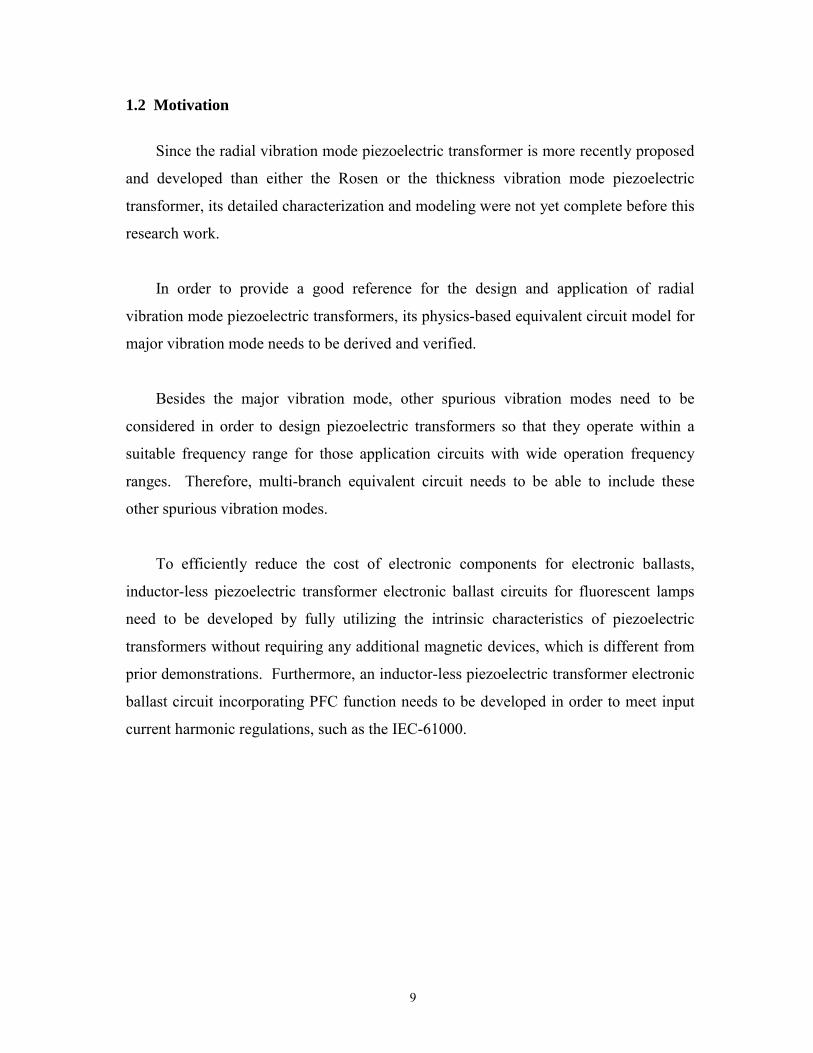
3.2 Measurement of Equivalent Circuit Model for Piezoelectric Transformers
The parameters of the physics-based equivalent circuit for piezoelectric
transformers, shown in Figure 3.1, can be verified by using an HP-4194 impedance
analyzer [A8].
Cd2
1:N+
Vin_
+Vout
_Cd1
R L C
Figure 3.1. Physics-based equivalent circuit model for piezoelectric transformers.
3.2.1 Y-Parameter Equivalent Circuit Model
The HP-4194A impedance analyzer provides a Y-parameter equivalent circuit
model, which is an admittance equivalent circuit, as shown in Figure 3.2. With the input
or output terminal shorted, the physics-based equivalent circuit is identical to the Y-
parameter equivalent circuit model shown in Figure 3.2. This Y-parameter equivalent
circuit model has been used to measure and characterize the equivalent circuit model of
piezoelectric transformers [A8].
R
L
Ca
Cb
Figure 3.2. Y-parameter equivalent circuit model provided by the HP-4194Aimpedance analyzer. This Y-parameter equivalent circuit model is anadmittance equivalent circuit and can be utilized to measure andcharacterize the equivalent circuit model of piezoelectric transformers[A8].

48
3.2.2 Measurement Procedure
Based on the Y-parameter equivalent circuit model provided by the HP-4194A
impedance analyzer, the parameters of the equivalent circuit model for piezoelectric
transformers around the resonant frequency range can be measured and characterized as
described in the following outline [A8, A9],
Step 1. By shorting the output terminal, Vout, of the piezoelectric transformer, input
admittance, Yin, can be measured by the HP4194A impedance analyzer. This
analyzer can then model this input admittance using the Y-parameter equivalent
circuit. The Y-parameter equivalent circuit includes four parameters, R1, L1,
Ca1 and Cb1, as shown in Figure 3.3A. The Y-parameter equivalent circuit is
identical to the equivalent circuit model of the piezoelectric transformer, but
with one terminal shorted. The four parameters of the equivalent circuit model
for piezoelectric transformers can be obtained as follows:
Cd1=Cb1 (3.1)
R=R1 (3.2)
L=L2 (3.3)
C=Ca1 (3.4)
Step 2. By shorting the output terminal, Vin, of the piezoelectric transformer, the output
admittance, Yout, can be measured by the HP-4194A impedance analyzer. The
analyzer can then model the output admittance, Yout, using the Y-parameter
equivalent circuit. This Y-parameter equivalent circuit includes four
parameters, R2, L2, Ca2 and Cb2, as shown in Figure 3.3B. Two parameters of
the equivalent circuit model, Cd2 and N, can be obtained as follows:
Cd2=Cb2 (3.5)
1L2L
N = (3.6)

49
HP4194A
ImpedanceAnalyzer
PiezoelectricTransformer
+Vin
+Vout
Yin
(a)
Cd2
1:N+
Vin_
+Vout
_Cd1
R L C
Yin Equivalent Circuit Model of Piezoelectric Transformer
(b)
R1
L1
Ca1
Cb1
Cd1=Cb1
R = R1
L = L1
C = Ca1Yin
(c)
Figure 3.3A. Step 1 of measurement procedure for equivalent circuit model ofpiezoelectric transformers. (a) setup for measuring input admittance,Yin. (b) equivalent circuit model with output terminal shorted. (c) Y-parameter equivalent circuit model provided by the HP-4194Aimpedance analyzer. With output terminal, Vout, shorted, theparameters, R, L, C and Cd1, can be measured and characterized usingthe Y-parameter equivalent circuit provided by the HP-4194Aimpedance analyzer.

50
HP4194A
ImpedanceAnalyzer
PiezoelectricTransformer
+Vout
+Vin
Yout(a)
Cd2
1:N+
Vin_
+Vout
_Cd1
R L C
YoutEquivalent Circuit Model of Piezoelectric Transformer
(b)
Cd2=Cb2
1L2L
N=
R2
L2
Ca2
Cb2
Yout
(c)
Figure 3.3B. Step 2 of measurement procedure for equivalent circuit model ofpiezoelectric transformers. (a) setup for measuring output admittance,Yout. (b) equivalent circuit model with input terminal shorted. (c) Y-parameter equivalent circuit model provided by HP-4194A impedanceanalyzer. With the output terminal, Vin, shorted, the parameters, N andCd2, can be measured and characterized using the Y-parameterequivalent circuit model provided by the HP-4194A impedanceanalyzer.

51
3.3 Measurement of Radial Vibration Mode Piezoelectric Transformer Samples
This section will use the characterization procedure described in the previous
section to measure the parameters of the equivalent circuits for the single-layer sample,
AS, and the multi-layer samples, CK2, CZ2, and CE1. These measured results will be
compared with the parameters of the derived physics-based equivalent circuit model for
radial vibration mode piezoelectric transformers.
3.3.1 Single-Layer Structure Samples
In order to verify the equivalent circuit model for the single-layer radial vibration
mode piezoelectric transformer discussed in the previous chapter, ten identical samples,
AS-1 to AS-10, were characterized, following the procedure outlined in Section 3.2.
The dimensions of these nine samples are identical, as follows:
Diameter, D= 825mil= 0.825 inch = 21mm;
Thickness of primary side, t1= 30mil= 0.030 inch = 0.76mm; and
Thickness of secondary side, t2= 90mil= 0.090 inch = 2.28mm.
Vin
VoutCeramic Layer
Ceramic Layer
rt2
t1
(r=412.5mil, t1=30mil, t2=90mil)
Figure 3.4. Single-layer radial vibration mode piezoelectric transformer sample,AS.
The coefficients of the piezoelectric material, APC 841 [D7], used for samples AS-1
to AS-10, are shown in Table 3.1. Figures 3.5, 3.6, 3.7, 3.8, 3.9 and 3.10 show the
comparisons of the measured results and the calculated results for respective parameters,
Cd1, Cd2, R, L, C and N, of the equivalent circuit model for the ten identical single-layer
radial vibration mode samples. Figure 3.11 shows the comparison of the modeled and

52
measured results for the resonant frequency, fo. The differences between the measured
and calculated results may result from the following factors:
(1) Tolerance of the piezoelectric ceramic coefficients,
(2) Tolerance of the dimensions,
(3) Additional mechanical losses due to the existence of the glue and copper layer.
Table 3.1. Coefficients of piezoelectric ceramic material, APC 841 [D7].
Coefficient Value
Density ρ=7.6 (g/cc)
Poissons Ratio σ=-0.32
Relative Dielectric Constant ε33T=1350εo
Mechanical Quality Factor Qm=1400
k31=0.33Coupling Coefficient
k33=0.68
d31=-109⋅10-12 (m/V)Piezoelectric Coefficient
d33=275⋅10-12 (m/V)
Y11E=7.6⋅1010 (N/m2)Youngs Modulus
Y33E=6.3⋅1010 (N/m2)
S11E=11.7⋅10-12 (m2/N)Elastic Compliance
S33E=17.3⋅10-12 (m2/N)
Shear Frequency Constant NL=1700 (m/s)
Thickness Frequency Constant NT=2005 (m/s)
Radial Frequency Constant Np=2055 (m/s)
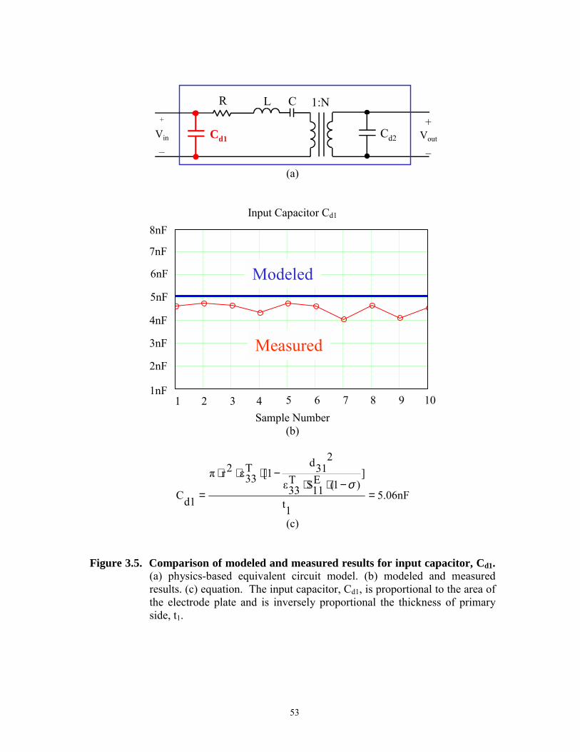
53
Cd2
1:N+
Vin_
+Vout
_Cd1
R L C
(a)
Input Capacitor Cd1
Measured
Modeled
8nF
7nF
4nF
3nF
6nF
5nF
2nF
1nF1 2 3 4 5 6 7 8 9 10
Sample Number(b)
5.06nF1t
])1(E
11ST33ε
231d
[1T33ε
2rπ
d1C =−⋅⋅
−⋅⋅⋅
=σ
(c)
Figure 3.5. Comparison of modeled and measured results for input capacitor, Cd1.(a) physics-based equivalent circuit model. (b) modeled and measuredresults. (c) equation. The input capacitor, Cd1, is proportional to the area ofthe electrode plate and is inversely proportional the thickness of primaryside, t1.

54
Cd2
1:N+
Vin_
+Vout
_Cd1
R L C
(a)
Output Capacitor Cd2
Measured
Modeled
2nF
1nF
1.5nF
1 2 3 4 5 6 7 8 9 10Sample Number
(b)
1.69nFt
]σ)(1E
11ST33ε
231d
[1T33ε
2rπ
d2C
2
=−⋅⋅
−⋅⋅⋅
=
(c)
Figure 3.6. Comparison of modeled and measured results for output capacitor,Cd2. (a) physics-based equivalent circuit model. (b) modeled andmeasured results. (c) equation. The physics-based component of theoutput capacitor, Cd2, is proportional to the area of the electrode plate andis inversely proportional the thickness of secondary side, t2.

55
Cd2
1:N+
Vin_
+Vout
_Cd1
R L C
Physics-based equivalent circuit model(a)
Resistor R
Measured
Modeled
15
10
5
01 2 3 4 5 6 7 8 9 10
Sample Number
(b)
Ω=⋅⋅
−⋅⋅⋅⋅
+= 04.4
231
dQm32
3σ)(13E
11Sρ2
r
)2
t1
(tR
(c)
Figure 3.7. Comparison of modeled and measured results for resistors, R. (a)physics-based equivalent circuit model. (b) modeled and measured results.(c) equation. The physics-based component of the resistor, R, isproportional to the total thickness, (t1+t2), and is inversely proportional toradius, r.

56
Cd2
1:N+
Vin_
+Vout
_Cd1
R L C
(a)
Inductor L
Measured
Modeled
12mH11mH
10mH
6mH
9mH
8mH
7mH
5mH1 2 3 4 5 6 7 8 9 10
Sample Number
(b)
9.1mH2
31dπ16
2σ)(12E
11Sρ
)2
t1
(tL =⋅⋅
−⋅⋅⋅+=
(c)
Figure 3.8. Comparison of modeled and modeled results for inductors, L. (a)physics-based equivalent circuit model. (b) modeled and measured results.(c) equation. The physics-based component of the inductor, L, isproportional to the total thickness, (t1+t2).

57
Cd2
1:N+
Vin_
+Vout
_Cd1
R L C
(a)
Capacitor C
Measured
Modeled
500pF
100pF
400pF
300pF
200pF
1 2 3 4 5 6 7 8 9 10Sample Number
(b)
284.4nFσ)(1E
11Sπ
231d
)2t1(t
2r32C =
−⋅⋅⋅
+
⋅=
(c)
Figure 3.9. Comparison of modeled and measured results for capacitor, C. (a)physics-based equivalent circuit model. (b) modeled and measured results.(c) equation. The physics-based component of capacitor, C, isproportional to the square of radius, r, and is inversely proportional to thetotal thickness, (t1+t2).

58
Cd2
1:N+
Vin_
+Vout
_Cd1
R L C
(a)
Turns Ratio N
1 2 3 4 5 6 7 8 9 100
0.5
1
1.5
2
Measured
Modeled
Sample Number
(b)
N=1(c)
Figure 3.10. Comparison of modeled and measured results for turns ratio, N. (a)physics-based equivalent circuit model. (b) calculated and measuredresults. (c) equation.

59
Cd2
1:N+
Vin_
+Vout
_Cd1
R L C
(a)
Resonant Frequency fo
50kHz
150kHz
100kHz
1 2 3 4 5 6 7 8 9 10
Measured
Modeled
Sample Number
(b)
kHz9.89CL2π
1fo =⋅
=
(c)
Figure 3.11. Comparison of modeled and measured results for resonant frequency,fo. (a) physics-based equivalent circuit model. (b) modeled and measuredresonant frequency, fo. (c) equation.

60
3.3.2 Multi-Layer Structure Samples
In order to verify the equivalent circuit model for the multi-layer radial vibration
mode piezoelectric transformer derived in the previous chapter, three different multi-
layer radial vibration mode piezoelectric transformer samples, CK2, CZ2 and CE1, will
be characterized, following the procedure outlined in Section 3.2. Figure 3.12 shows the
cross-sections of the multi-layer radial vibration mode piezoelectric transformer samples
CK2, CZ1 and CE1.
D
t1t2t3
+Vout
_Vin t1
t2
t3
(a)
V i n
V o u t
t 1
t 2
t 3
t 4
t 5
(b)
Vin
Vout
t1
t2
t3
t4
t5
(c)
Figure 3.12. Cross-sections of multi-layer radial vibration mode piezoelectrictransformer samples. (a) sample CK2 (t1=t2=t3=80mils, D=1180mils,n1=2, n2=1). (b) sample CZ2 (t1=t2=t3=t4= t5= 20mils, D=1180mils, n1=4,n2=1). (c) sample CE1 (t1=t2=t3=t4=t5=80mils, D=1180mils, n1=4, n2=1).

61
Table 3.2 shows the dimensions of the samples. Table 3.3 shows the coefficients
of the piezoelectric ceramic material, PKI-802 [D9], used for the samples. Table 3.4
shows the modeled parameters, R, L, C, N, Cd1 and Cd2, of the physics-based equivalent
circuit models for these three samples, compared with the measured results of the
characterized equivalent circuits. Referring to Table 3.4, the modeled resistor value, R,
is much smaller than the measured result because the actual resistor value includes not
only the piezoelectric vibration losses, but also the mechanical interface losses. The
calculated turns ratio values of samples CK 2 and CZ2 very closely match their
measured turns ratio values. However, the measured turns ratio of CE1 is 4.97, which is
larger than the modeled value, 4, even though the diameter and layer number of sample
CE1 are the same as those of CZ2 but with different layer thickness. This deviation can
be caused by the interaction between radial vibration and thickness vibration modes in
the five-layer sample CE1 when the mechanical vibration wavelengths of radial mode
and thickness mode are very close. As stated in Section 2.4, the physics-based
equivalent circuit model of radial vibration mode piezoelectric transformers was derived
under the assumption of radial vibration mode only and without considering other
vibration modes. Therefore, the derived physics-based equivalent circuit model agrees
with the corresponding measured results when the total thickness is much less than the
radius.
Table 3.2. Dimensions of multi-layer radial vibration mode piezoelectrictransformer samples, CK2, CZ2, and CE1.
Primary Side Secondary Side
Sample Diameter(mil)
LayerNumber
Layer Thickness(mil)
LayerNumber
Layer Thickness(mil)
CK2 1,180 2 t1 =t2 =80 1 t3 =80CZ2 1,180 4 t1 =t2 =t3 =t4 = 20 1 t5= 20CE1 1,180 4 t1 =t2 =t3 =t4 = 80 1 t5= 80
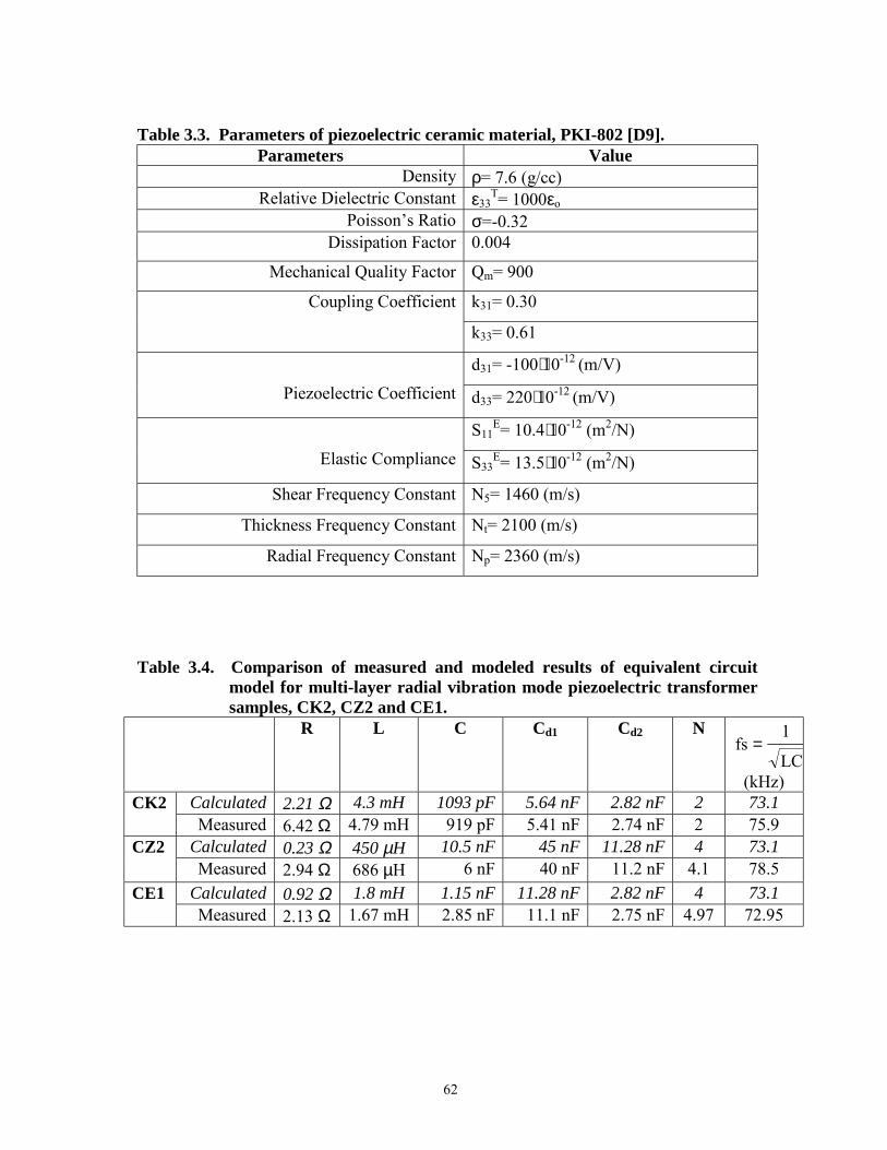
62
Table 3.3. Parameters of piezoelectric ceramic material, PKI-802 [D9].Parameters Value
Density ρ= 7.6 (g/cc)Relative Dielectric Constant ε33
T= 1000εoPoissons Ratio σ=-0.32
Dissipation Factor 0.004
Mechanical Quality Factor Qm= 900
k31= 0.30Coupling Coefficient
k33= 0.61
d31= -100⋅10-12 (m/V)
Piezoelectric Coefficient d33= 220⋅10-12 (m/V)
S11E= 10.4⋅10-12 (m2/N)
Elastic Compliance S33E= 13.5⋅10-12 (m2/N)
Shear Frequency Constant N5= 1460 (m/s)
Thickness Frequency Constant Nt= 2100 (m/s)
Radial Frequency Constant Np= 2360 (m/s)
Table 3.4. Comparison of measured and modeled results of equivalent circuitmodel for multi-layer radial vibration mode piezoelectric transformersamples, CK2, CZ2 and CE1.
R L C Cd1 Cd2 N
LC
1fs =
(kHz)Calculated 2.21 Ω 4.3 mH 1093 pF 5.64 nF 2.82 nF 2 73.1CK2Measured 6.42 Ω 4.79 mH 919 pF 5.41 nF 2.74 nF 2 75.9
Calculated 0.23 Ω 450 µH 10.5 nF 45 nF 11.28 nF 4 73.1CZ2Measured 2.94 Ω 686 µH 6 nF 40 nF 11.2 nF 4.1 78.5
Calculated 0.92 Ω 1.8 mH 1.15 nF 11.28 nF 2.82 nF 4 73.1CE1Measured 2.13 Ω 1.67 mH 2.85 nF 11.1 nF 2.75 nF 4.97 72.95

63
3.4 Improved Accuracy of Equivalent Circuit Model
Besides the major vibration mode, there are many other spurious vibration modes in
piezoelectric transformers. Figure 3.13 shows the voltage gain comparison of the
measured result and the single-branch model, as discussed in Section 3.3.2, for the radial
vibration mode piezoelectric transformer sample CK2 with RL=600Ω. This comparison
shows that the single-branch model can only match the major vibration mode within a
specific frequency range of 60kHz to 90kHz. Above 90 kHz and below 60kHz, the
modeled voltage gain curve deviates from that of the measured voltage gain. Obviously,
this single-branch model may lead to the wrong voltage gain result in actual circuit
designs. In order to model the true voltage gain of piezoelectric transformers for wider
frequency ranges, it is necessary to have a more precise equivalent circuit model for
circuit design.
Voltage gains with RL=600Ω
4 4 4 4 4 4 4 4 4 5 5 5 5 5 5 5 5 580
70
60
50
40
30
20
10
0
10
20
50kHz 100kHz 150kHz 190kHz10kHz
Single-branch Model
Measured
dBinVoutV
Frequency
Figure 3.13. Voltage gains of measured result and single-branch equivalent circuitmodel. The single-branch model, discussed in Section 3.2.2, can onlymatch the major vibration mode within a specific frequency range.

64
3.4.1 Prior Model
In order to describe the vibration mode at the major resonant frequency as well as
other spurious vibration modes for piezoelectric transformers, prior work [A8]
developed a multi-branch equivalent circuit model, as shown in Figure 3.14. This model
has more R-L-C branches to describe other spurious vibration modes.
With the output terminal, Vout, shorted, the input admittance, Yin, of sample CK2
can be measured, as shown in Figure 3.15. Referring to Figure 3.15, there are four
spurious vibration modes, fr1, fr2, fr3 and fr4, in addition to the major radial vibration
mode, fr, within the frequency range of 10kHz to 200kHz. With the frequency ranges
corresponding to different vibration modes, as shown in Figure 3.16, each vibration
mode can be characterized by a different Y-parameter equivalent circuit model, as
shown in Table 3.5. Spurious vibration modes, fr1 and fr3, can result from spurious
radial vibrations. Spurious vibration modes, fr2 and fr4, can result from spurious
thickness vibrations. Table 3.5 shows that each vibration mode is represented by one
corresponding R-L-C network branch with a different turns ratio. However, the multi-
branch equivalent circuit based on the prior approach [A8], as shown in Figure 3.17,
only uses the turns ratio of the major radial vibration mode while ignoring the other
turns ratios of the spurious vibration modes. The parameters of this prior equivalent
circuit model for sample CK2 are listed in Table 3.6.
Although the multi-branch equivalent circuit model based on the prior approach
matches the measured input admittance curve Yin, as shown in Figure 3.18, there is quite
a deviation in the respective voltage gain curves, as shown in Figure 3.19. It is apparent
that the prior multi-branch equivalent circuit model needs some modification in order to
more precisely match the measured voltage gain curve of radial vibration mode
piezoelectric transformers. Toward this goal, the next section will propose an improved
multi-branch equivalent circuit model.

65
Cd2
1:N+
Vin_
Cd1
R L C
R1 L1 C1
R2 L2 C2
R4 L4 C4
R3 L3 C3
RL
CL2π
10
LRfr
⋅==
1C1L2π
10
LR1fr
⋅==
3C3L2π
10
LR3fr
⋅==
2C2L2π
10
LR2
fr⋅
==4C4L2π
10
LR4fr
⋅==
Figure 3.14. Multi-branch equivalent circuit model for piezoelectric transformers[A8]. This model describes the major resonant vibration mode at themajor resonant frequency, fr, and other spurious resonant vibration modesat other spurious resonant frequencies, fr1, fr2, fr3 and fr4.

66
HP4194A
ImpedanceAnalyzer
Radial Vibration ModePiezoelectricTransformer
+Vin
+Vout
Yin
(a)
10kHz 50kHz 100kHz 150kHz 200kHz
0.15
0.10
0.05
fr
fr1 fr2 fr3fr4
Frequency
(b)
Figure 3.15. Measured input admittance of radial vibration mode piezoelectrictransformer sample CK2. (a) measurement setup. (b) magnitude ofinput admittance Yin (mho). Within the frequency range from 10kHz to200kHz, there are four spurious vibration frequencies, fr1, fr2, fr3 andfr4, in addition to the major radial vibration mode resonant frequency, fr.
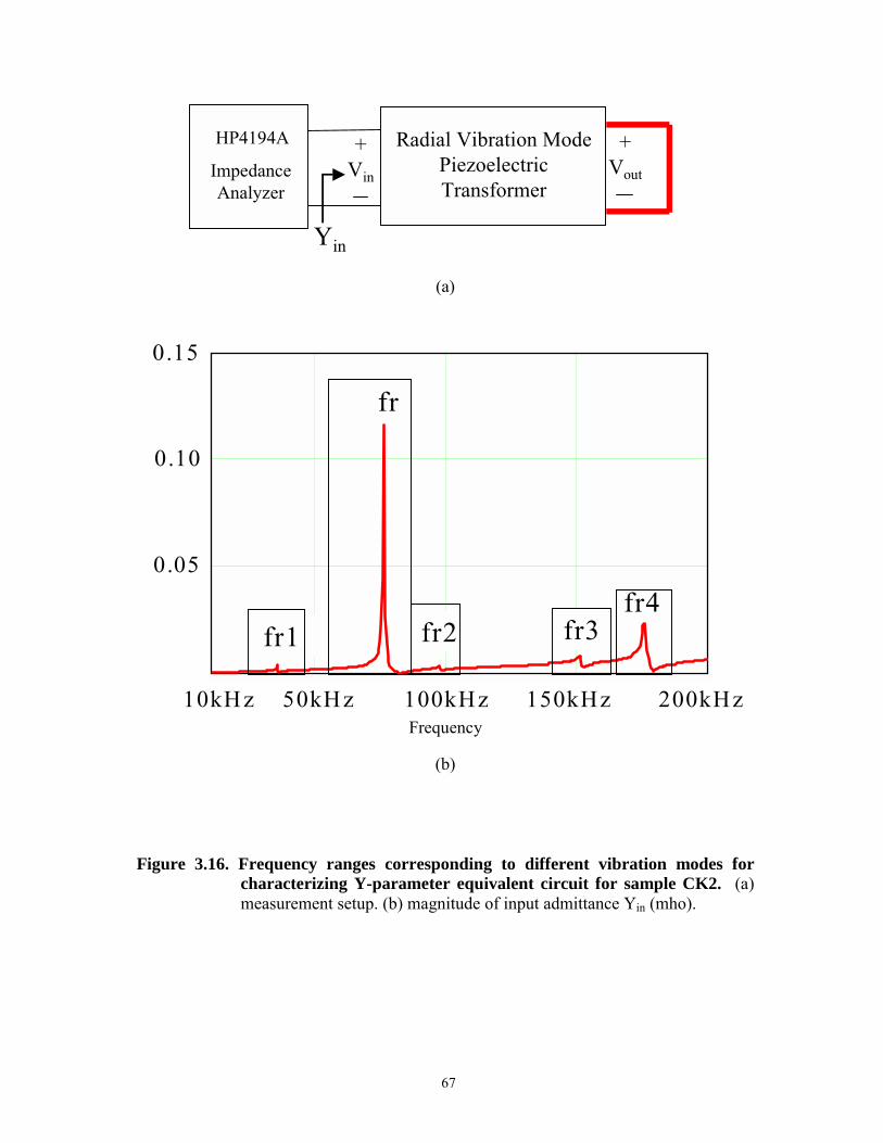
67
HP4194A
ImpedanceAnalyzer
Radial Vibration ModePiezoelectricTransformer
+Vin
+Vout
Yin
(a)
10kHz 50kHz 100kHz 150kHz 200kHz
0.15
0.10
0.05
fr
fr1 fr2 fr3fr4
Frequency
(b)
Figure 3.16. Frequency ranges corresponding to different vibration modes forcharacterizing Y-parameter equivalent circuit for sample CK2. (a)measurement setup. (b) magnitude of input admittance Yin (mho).

68
Table 3.5. Measured parameters of Y-parameter equivalent circuits forradial vibration mode piezoelectric transformer sample CK2.
(10kHz to 200kHz) Y-Parameter Equivalent CircuitsResonant Frequency Input Admittance
Yin
OutputAdmittance
Yout
TurnsRatio
R1s = 6.42Ω R2s = 29.84Ω
L1s = 4.79mH L2s = 20.75mH
C1s = 918.71pF C2s = 211.44pF78.7kHzr2
pN
kHz87.751sC1sL
1fr
=⋅
≈
=⋅
=
(Major Radial Vibration Mode) Cb1s = 5.41nF Cb2s = 2.74nF2
1sL
2sL
N
=
=
R1s1 = 103.93Ω R2s1 = 112.31Ω
L1s1 = 112.36mH L2s1 = 126.21mH39.4kHz
r4pN
kHz9.531s1C1s1L
1fr1
=⋅
≈
=⋅
=
(Spurious Radial Vibration Mode) C1s1= 181.215pF C2s1 = 161.296pF
04.11s1
L2s1
LN1
=
=
R1s2 = 368.23Ω R2s2 = 365.9Ω
L1s2 = 52.32mH L2s2 = 66.07mH
86.1kHzt12
tN
kHz5.791s2C1s2L
1fr2
=⋅
≈
=⋅
=
(Spurious Thickness Vibration Mode) C1s2 = 50.92pF C2s2 = 40.27pF
1.11s2
L2s2
LN2
=
=
R1s3 = 184.76Ω R2s3 = 218.2Ω
L1s3 = 20.3536mH L2s3 = 23.16mH
157.5kHzrpN
kHz3.5111s3C1s3L
1fr3
=≈
=⋅
=
(Spurious Radial Vibration Mode)C1s3= 54.3587pF C2s3 = 47.73pF
06.11s3
L2s3
LN3
=
=
R1s4= 42.75Ω R2s4 = 264.67Ω
L1s4= 4.81mH L21s4 = 27.97mH
172.2kHzt6tN
kHz8.7511s4C1s4L
1fr4
=⋅
≈
=⋅
=
(Spurious Thickness Vibration Mode)C1s4= 170.25pF C2s4 = 28.34pF
4.21s4
L2s4
LN4
=
=
Note: r is the radius of sample CK2,t is the layer thickness of sample CK2,Np is the radial frequency constant of the piezoelectric material, andNt is the thickness frequency constant of the piezoelectric material.

69
Table 3.6. Characterized parameters of prior multi-branch equivalent circuitmodel for radial vibration mode piezoelectric transformer sample CK2.Resonant Frequency Parameter Characterized Value
Cd1 5.41nFR 6.42ΩL 4.79mHC 918.71pFN 278.7kHz
r2pN
kHz87.751sC1sL
1fr
=⋅
≈
=⋅
=
(Major Radial Vibration Mode) Cd2 2.74nFR1 103.93Ω
L1 112.36mH
39.4kHzr4pN
kHz9.531s1C1s1L
1fr1
=⋅
≈
=⋅
=
(Spurious Radial Vibration Mode) C1 181.2pF
R2 368.23Ω
L2 52.32mH86.1kHz
t12tN
kHz5.791s2C1s2L
1fr2
=⋅
≈
=⋅
=
(Spurious Thickness Vibration Mode) C2 50.92pF
R3 184.76Ω
L3 20.3536mH157.5kHz
rpN
kHz3.5111s3C1s3L
1fr3
=≈
=⋅
=
(Spurious Radial Vibration Mode) C3 54.3587pFR4 42.75ΩL4 4.81mH
172.2kHzt6tN
kHz8.7511s4C1s4L
1fr4
=⋅
≈
=⋅
=
(Spurious Thickness Vibration Mode)
C4 170.25pF
Note: r is the radius of sample CK2,t is the layer thickness of sample CK2,Np is the radial frequency constant of the piezoelectric material, andNt is the thickness frequency constant of the piezoelectric material.

70
R1 L1 C1
104Ω 112mH 181pF
R4 L4 C4
42Ω 4.8mH 170pF
L2 C2R2
368Ω 52mH 50pF
R3 L3 C3
184Ω 20mH 54pF
1:2
Cd1Cd2
+Vin-
+Vout
-RL
6.42Ω 4.79mH 918pF
5.4nF2.84nF 600Ω
Figure 3.17. Multi-branch equivalent circuit model for the radial vibration modepiezoelectric transformer sample, CK2, based on prior approach [A8].This multi-branch equivalent circuit is composed of five R-L-C branches.Each vibration mode is represented by one corresponding R-L-C branch.

71
R1 L1 C1
104Ω 112mH 181pF
R4 L4 C4
42Ω 4.8mH 170pF
L2 C2R2
368Ω 52mH 50pF
R3 L3 C3
184Ω 20mH 54pF
1:2
Cd1Cd2
+Vin-
6.42Ω 4.79mH 918pF
5.4nF2.84nF
Outputshorted
(a)
10kHz 50kHz 100kHz 150kHz 200kHz
0.15
0.10
0.05
MeasuredModelfr
fr1 fr2 fr3fr4
(b)
Figure 3.18. Comparison of measured and prior model input admittance curvesfor sample CK2. (a) multi-branch equivalent circuit model based onprior approach [A8]. (b) magnitude of input admittance (mho). The priormulti-branch equivalent circuit model can very closely match themeasured input admittance curve, Yin.

72
R1 L1 C1
104Ω 112mH 181pF
R4 L4 C4
42Ω 4.8mH 170pF
L2 C2R2
368Ω 52mH 50pF
R3 L3 C3
184Ω 20mH 54pF
1:2
Cd1Cd2
+Vin-
+Vout
-RL
6.42Ω 4.79mH 918pF
5.4nF2.84nF 600Ω
(a)
Voltage gains with RL=600Ω
50kHz 100kHz 150kHz 190kHz10kHz80
70
60
50
40
30
20
10
0
10
20
MeasuredModel
dB
inVoutV
(b)
Figure 3.19. Comparison of measured voltage gain and modeled result for radialvibration mode piezoelectric transformer sample CK2 with RL=600ΩΩΩΩ.(a) prior multi-branch Equivalent circuit model [A8]. (b) measured andmodeled results of voltage gains. The modeled voltage gain is based on aprior multi-branch equivalent circuit model [A8]. However, there is quitea deviation in the respective voltage gain curve.

73
3.4.2 Improved Model
Although the prior multi-branch equivalent circuit model based on the prior
approach [A8] can very closely match the measured input admittance curve, Yin, there is
still quite a deviation in the respective voltage gain curves, as found in the last section.
Since different vibration modes have different voltage gains and phases, as shown in
Figure 3.20, the prior model cannot simply utilize one common ideal transformer to
describe all the vibration modes within a specific frequency range. Figures 3.21 to 3.25
show the voltage gains and phases of different vibration modes, fr, fr1, fr2, fr3 and fr4,
according to the parameters of the characterized Y-parameter equivalent circuits shown
in Table 3.5. These figures show that the polarities of turns ratios, N, N1, N2, N3, and
N4, for each single equivalent circuit network can affect the deviation of the phase
curve. Figure 3.26 shows the voltage gain and phase curves of the multi-branch
equivalent circuit of vibration modes, fr and fr2, with the correct polarities for their turns
ratio, N and N2. Figure 3.27 shows the voltage gain and phase curves of the multi-
branch equivalent circuit of vibration modes, fr, fr1, and fr2, with the correct polarities
for their turns ratios, N and N2.
In order to more precisely describe the measured voltage gain, the prior multi-
branch equivalent circuit model can be improved by accounting for the phase and branch
gain ratio characteristics of all of the vibration modes, as shown in Figure 3.28. The
parameters of the improved model for sample CK2 are shown in Table 3.7. This
improved model can match the measured voltage gain curve much more accurately than
the prior multi-branch equivalent circuit model, as shown in Figures 3.29 and 3.30. The
improved circuit model uses more detailed networks to describe the voltage gains and
phases of various spurious vibration modes for radial vibration mode piezoelectric
transformers.

74
D
t1t2t3
+Vout
_Vin t1
t2
t3
RL
(t1= t2= t3 = 80mils, D= 1180mils)n1= 2, n2= 1
(a)
80
70
60
50
40
30
20
10
0
10
20
50kHz 100kHz 150kHz 190kHz10kHz
dB
inVoutV
(b)
1080102096090084078072066060054048042036030024018012060
060
120180
50kHz 100kHz 150kHz 190kHz10kHz
Degree
inVoutV
(c)
Figure 3.20. Measured voltage gain and phase of sample CK2. (a) sample CK2 withRL=600Ω. (b) voltage gain (dB). (c) phase (Degree).

75
Cd1 Cd2
1:N
+Vin-
R L C
+Vout
-RL
6.42Ω 4.79mH 918pF
5.4nF2.84nF 600Ω
(a)
50kHz 100kHz 150kHz 190kHz10kHz80
70
60
50
40
30
20
10
0
10
20
MeasuredModel
dB
inVoutV
(b)
1080102096090084078072066060054048042036030024018012060
060
120180
0
0
50kHz 100kHz 150kHz 190kHz10kHz
MeasuredModel
Degree
inVoutV
(c)
1080102096090084078072066060054048042036030024018012060
060
120180
0
0
50kHz 100kHz 150kHz 190kHz10kHz
MeasuredModel
Degree
inVoutV
(d)
Figure 3.21. Voltage gain and phase of major vibration mode, fr. (a) equivalentcircuit of major vibration mode, fr. (b) voltage gain (N= +2 or 2). (c)phase (N= -2). (d) phase (N= +2).

76
Cd1 Cd2
1:N1
+Vin-
R1 L1 C1
+Vout
-RL
104Ω 112mH 181pF
5.4nF2.84nF 600Ω
(a)
80
70
60
50
40
30
20
10
0
10
20
MeasuredModel
dB
inVoutV
(b)
1080102096090084078072066060054048042036030024018012060
060
120180
0
0
2
50kHz 100kHz 150kHz 190kHz10kHz
MeasuredModel
Degree
inVoutV
(c)
1080102096090084078072066060054048042036030024018012060
060
120180
0
0
50kHz 100kHz 150kHz 190kHz10kHz
MeasuredModel
Degree
inVoutV
(d)
Figure 3.22. Voltage gain and phase of spurious vibration mode, fr1. (a) equivalentcircuit of spurious vibration mode, fr1. (b) voltage gain (N1= +1.04 or 1.04). (c) phase (N1= +1.04). (d) phase (N1= -1.04).

77
Cd1 Cd2
1:N2
+Vin-
R2 L2 C2
+Vout
-RL
368Ω 52mH 50pF
5.4nF2.84nF 600Ω
(a)
80
70
60
50
40
30
20
10
0
10
200
0
)
50kHz 100kHz 150kHz 190kHz10kHz
MeasuredModel
dB
inVoutV
(b)
1080102096090084078072066060054048042036030024018012060
060
120180
0
0
50kHz 100kHz 150kHz 190kHz10kHz
MeasuredModel
Degree
inVoutV
(c)
1080102096090084078072066060054048042036030024018012060
060
120180
0
0
2
50kHz 100kHz 150kHz 190kHz10kHz
MeasuredModel
Degree
inVoutV
(d)
Figure 3.23. Voltage gain and phase of spurious vibration mode, fr2. (a) equivalentcircuit of spurious vibration mode, fr2. (b) voltage gain (N2= +1.1 or 1.1). (c) phase (N2= +1.1). (d) phase (N2= -1.1) .
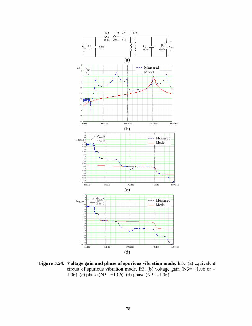
78
Cd1 Cd2
1:N3
+Vin-
R3 L3 C3
+Vout
-RL
184Ω 20mH 54pF
5.4nF2.84nF 600Ω
(a)
80
70
60
50
40
30
20
10
0
10
20
50kHz 100kHz 150kHz 190kHz10kHz
MeasuredModel
dB
inVoutV
(b)
1080102096090084078072066060054048042036030024018012060
060
120180
0
0
50kHz 100kHz 150kHz 190kHz10kHz
MeasuredModel
Degree
inVoutV
(c)
1080102096090084078072066060054048042036030024018012060
060
120180
0
50kHz 100kHz 150kHz 190kHz10kHz
MeasuredModel
Degree
inVoutV
(d)
Figure 3.24. Voltage gain and phase of spurious vibration mode, fr3. (a) equivalentcircuit of spurious vibration mode, fr3. (b) voltage gain (N3= +1.06 or 1.06). (c) phase (N3= +1.06). (d) phase (N3= -1.06).

79
Cd1 Cd2
1:N4
+Vin-
R4 L4 C4
+Vout
-RL
42Ω 4.8mH 170pF
5.4nF2.84nF 600Ω
(a)
80
70
60
50
40
30
20
10
0
10
20
50kHz 100kHz 150kHz 190kHz10kHz
MeasuredModel
dB
inVoutV
(b)
4 4 4 4 4 4 4 4 4 5 5 5 5 5 5 5 5 51080102096090084078072066060054048042036030024018012060
060
120180
0
0
2
50kHz 100kHz 150kHz 190kHz10kHz
MeasuredModel
Degree
inVoutV
(c)
1080102096090084078072066060054048042036030024018012060
060
120180
50kHz 100kHz 150kHz 190kHz10kHz
MeasuredModel
Degree
inVoutV
(d)
Figure 3.25. Voltage gain and phase of spurious vibration mode, fr4. (a) equivalentcircuit of spurious vibration mode, fr4. (b) voltage gain (N4= +2.4 or 2.4). (c) phase (N4= -2.4) (d) phase (N4= +2.4).

80
Cd1 Cd2
1:2
+Vin-
+Vout
-RL
6.42Ω 4.79mH 918pF
5.4nF2.84nF 600Ω
1:1.1R2 L2 C2
368Ω 52mH 50pF
R L C
(a)
80
70
60
50
40
30
20
10
0
10
200
0
)
50kHz 100kHz 150kHz 190kHz10kHz
MeasuredModel
dB
inVoutV
(b)
4 4 4 4 4 4 4 4 4 5 5 5 5 5 5 5 5 51080102096090084078072066060054048042036030024018012060
060
120180
0
0
50kHz 100kHz 150kHz 190kHz10kHz
MeasuredModel
Degree
inVoutV
(c)
Figure 3.26. Voltage gain and phase of multi-branch equivalent circuit of vibrationmodes, fr and fr2. (a) multi-branch equivalent circuit of vibration modes,fr and fr2. (b) voltage Gain (N= -2 and N2= 1.1). (c) phase (N= -2 andN2= 1.1).
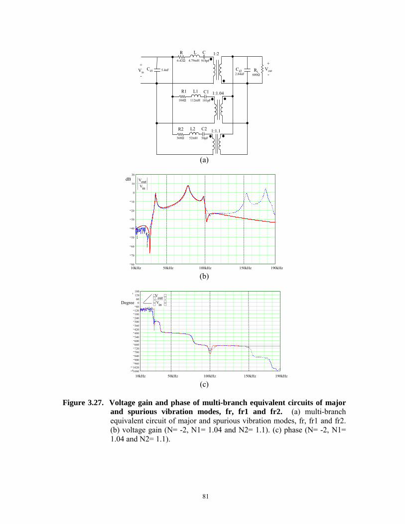
81
Cd1 Cd2
1:2
+Vin-
+Vout
-RL
6.42Ω 4.79mH 918pF
5.4nF2.84nF 600Ω
L2 C2 1:1.1R2
368Ω 52mH 50pF
1:1.04R1 L1 C1
104Ω 112mH 181pF
LR C
(a)
80
70
60
50
40
30
20
10
0
10
20
50kHz 100kHz 150kHz 190kHz10kHz
dB
inVoutV
(b)
1080102096090084078072066060054048042036030024018012060
060
120180
0
0
2
50kHz 100kHz 150kHz 190kHz10kHz
Degree
inVoutV
(c)
Figure 3.27. Voltage gain and phase of multi-branch equivalent circuits of majorand spurious vibration modes, fr, fr1 and fr2. (a) multi-branchequivalent circuit of major and spurious vibration modes, fr, fr1 and fr2.(b) voltage gain (N= -2, N1= 1.04 and N2= 1.1). (c) phase (N= -2, N1=1.04 and N2= 1.1).

82
D
t1t2t3
+Vout
_Vin t1
t2
t3
RL
(t1= t2= t3 = 80mils, D= 1180mils, n1= 2, n2= 1)(a)
Cd1 Cd2
1:2
+Vin-
+Vout
-RL
6.42Ω 4.79mH 918pF
5.4nF2.84nF 600Ω
L2 C2 1:1.1R2
368Ω 52mH 50pF
1:1.04R1 L1 C1
104Ω 112mH 181pF
1:1.06R3 L3 C3
184Ω 20mH 54pF
1:2.4R4 L4 C4
42Ω 4.8mH 170pF
(b)
Figure 3.28. Improved multi-branch equivalent circuit model for radial vibrationmode piezoelectric transformer sample CK2. (a) sample CK2 withRL=600Ω. (b) improved equivalent circuit model.
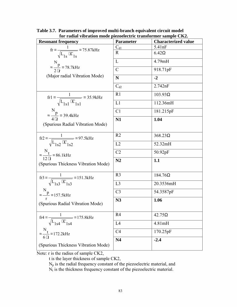
83
Table 3.7. Parameters of improved multi-branch equivalent circuit modelfor radial vibration mode piezoelectric transformer sample CK2.
Resonant frequency Parameter Characterized valueCd1 5.41nFR 6.42Ω
L 4.79mH
C 918.71pF
N -2
78.7kHzr2
pN
kHz87.751sC1sL
1fr
=⋅
≈
=⋅
=
(Major radial Vibration Mode)
Cd2 2.742nF
R1 103.93Ω
L1 112.36mH
C1 181.215pF39.4kHz
r4pN
kHz9.531s1C1s1L
1fr1
=⋅
≈
=⋅
=
(Spurious Radial Vibration Mode)N1 1.04
R2 368.23Ω
L2 52.32mH
C2 50.92pF86.1kHz
t12tN
kHz5.791s2C1s2L
1fr2
=⋅
≈
=⋅
=
(Spurious Thickness Vibration Mode)N2 1.1
R3 184.76Ω
L3 20.3536mH
C3 54.3587pF157.5kHz
rpN
kHz3.5111s3C1s3L
1fr3
=≈
=⋅
=
(Spurious Radial Vibration Mode)N3 1.06
R4 42.75Ω
L4 4.81mH
C4 170.25pF172.2kHzt6tN
kHz8.7511s4C1s4L
1fr4
=⋅
≈
=⋅
=
(Spurious Thickness Vibration Mode)N4 -2.4
Note: r is the radius of sample CK2,t is the layer thickness of sample CK2,Np is the radial frequency constant of the piezoelectric material, andNt is the thickness frequency constant of the piezoelectric material.

84
Cd1 Cd2
1:2
+Vin-
+Vout
-RL
6.42Ω 4.79mH 918pF
5.4nF2.84nF 600Ω
L2 C2 1:1.1R2
368Ω 52mH 50pF
1:1.04R1 L1 C1
104Ω 112mH 181pF
1:1.06R3 L3 C3
184Ω 20mH 54pF
1:2.4R4 L4 C4
42Ω 4.8mH 170pF
(a)
4 4 4 4 4 4 4 4 4 5 5 5 5 5 5 5 5 580
70
60
50
40
30
20
10
0
10
20
50kHz 100kHz 150kHz 190kHz10kHz
MeasuredProposed Model
dB
inVoutV
(b)
Figure 3.29. Comparison of voltage gains between the measured result and theimproved multi-branch equivalent circuit model for radial vibrationmode piezoelectric transformer sample, CK2. (a) improved multi-branch equivalent circuit model. (b) voltage gain curves of the measuredresult and the improved model. The improved model more accuratelymatches the measured voltage gain curve than the prior model.

85
Cd1 Cd2
1:2
+Vin-
+Vout
-RL
6.42Ω 4.79mH 918pF
5.4nF2.84nF 600Ω
L2 C2 1:1.1R2
368Ω 52mH 50pF
1:1.04R1 L1 C1
104Ω 112mH 181pF
1:1.06R3 L3 C3
184Ω 20mH 54pF
1:2.4R4 L4 C4
42Ω 4.8mH 170pF
(a)
1080102096090084078072066060054048042036030024018012060
060
120180
0
0
2
50kHz 100kHz 150kHz 190kHz10kHz
Degree
inVoutV
MeasuredProposed Model
(b)
Figure 3.30. Comparison of phase between measured result and improved multi-branch equivalent circuit model for radial vibration Modepiezoelectric transformer sample CK2. (a) improved multi-branchequivalent circuit model. (b) voltage phase curves of measured result andimproved model. This improved model matches the measured phasecurve with acceptable deviation.
86
3.5 Summary
By utilizing the Y-parameter equivalent circuit model provided by the HP4194A
impedance analyzer, this chapter has characterized the samples of radial vibration mode
piezoelectric transformer in order to verify the physics-based equivalent circuit model
derived in Chapter 2 for the major vibration mode. The comparison results showed that
the physics-based equivalent circuit model is in good agreement with the corresponding
measured results of the piezoelectric transformer samples when the total thickness is
much less than the radius.
Besides the major vibration mode, piezoelectric transformers have many spurious
vibration modes in other frequency ranges. These vibration modes can be characterized
with a multi-branch equivalent circuit model, composed of several single L-C resonant
tanks, for the design and simulation of application circuits operating in wide frequency
ranges rather than the major vibration mode. In order to more precisely characterize
radial vibration mode piezoelectric transformers, this chapter has proposed an improved
multi-branch equivalent circuit model to replace the prior circuit model. Although the
prior circuit model can very precisely characterize the input admittance, it cannot
characterize the voltage gain within an acceptable deviation. The improved multi-branch
equivalent circuit model uses more detailed networks to describe the gain ratios and
polarities of different spurious vibration modes for radial vibration mode piezoelectric
transformers. Therefore, the proposed improved multi-branch equivalent circuit model
can characterize the input admittance and voltage gain of radial vibration mode
piezoelectric transformer much more precisely than the prior model. The comparison of
the measured and modeled results showed that the improved model matches the
measured phase curve much better than the prior multi-branch equivalent circuit model
for radial vibration mode piezoelectric transformers.

87
CHAPTER 4
INDUCTOR-LESS PIEZOELECTRIC TRANSFORMER
ELECTRONIC BALLAST
4.1 Introduction
Because of high efficacy and long life, fluorescent lamps are becoming more
popular than incandescent lamps for residential and commercial uses. Ballast circuits
for driving fluorescent lamps can be categorized as either magnetic or electronic. Since
magnetic ballasts are bulky and emit an audible low-frequency humming noise,
electronic ballasts are more appealing and are produced in greater numbers than almost
any other electronic product of their type. However, the price of electronic ballasts is
still not low enough to attract all residential and commercial users. In order to lower the
price, most lighting companies worldwide have focused their efforts on finding cost-
effective component suppliers. Fortunately, piezoelectric transformers provide a good
alternative.
Figure 4.1 shows one typical electronic ballast circuit that uses an L-C resonant
tank to generate high voltage for igniting and sustaining a linear fluorescent lamp. This
L-C resonant tank is composed of resonant inductor L, DC-blocking capacitor C, a
voltage step-up transformer, and high-voltage resonant capacitor Cd2. Input capacitor
Cd1 works as an additional turn-off snubber capacitor for half-bridge switches S1 and S2.
The cost of these five passive components constitutes the major cost of the conventional
electronic ballast. However, the L-C resonant tank of the conventional electronic ballast
shown in Figure 4.1 is almost identical to the equivalent circuit of the piezoelectric
transformer shown in Figure 4.2, except for the addition of the resistor, R, in the latter.

88
Generally speaking, this resistance R is negligible as compared with the equivalent turn-
on resistance of fluorescent lamps.
S1
S1
VDC
Cs1
Cs2Lamp
L C 1:N
Cd2
+
Vout _
LC Resonant Tank
Cd1
Figure 4.1. Typical conventional electronic ballast circuit. This circuit employs atypical L-C resonant tank circuit and an additional turn-off snubbercapacitor Cd1 for half-bridge switches, S1 and S2.
1:NR CL
Cd2 VoutCd1Vout VoutVin
Figure 4.2. Equivalent circuit model of piezoelectric transformers. Components R,L and C are the equivalent physics-based components analogous toelectrical terms. Compared with the equivalent turn-on resistance offluorescent lamps, the resistance, R, in the equivalent circuit model can beignored.

89
Many prior technologies [B1-B13] tried to utilize piezoelectric transformers to
develop converter, inverter or electronic ballasts. Because of input capacitor Cd1, these
previous topologies required additional magnetic device(s), such as an inductor, in order
to enable their switches to work in ZVS condition. By using this prior approach, the
specific characteristics of the piezoelectric transformers were not fully utilized, and thus
extra expenses were incurred for the additional magnetic device(s). For example, Figure
4.3 shows a conventional piezoelectric transformer DC/DC converter utilizing a
thickness vibration mode piezoelectric transformer [A9]. Because the input capacitor
Cd1 is equal to 2.6nF, this converter must use additional inductors, Lr and Ls, to have its
switches, S1 and S2, working in ZVS condition. Since the equivalent circuit of
piezoelectric transformers has an inductor, this inductor may be utilized to have the half-
bridge switches operate in ZVS condition in order to save the additional inductor, Ls.
Furthermore, the input capacitor, Cd1, may be utilized as a turn-off snubber capacitor for
the half-bridge switches, S1 and S2. Therefore, this chapter will propose ZVS criteria to
evaluate the equivalent circuit models of piezoelectric transformers for the required ZVS
condition.
Based on the proposed ZVS criteria, this chapter will first present the design and
implementation of a cost-effective inductor-less piezoelectric transformer electronic
ballast employing a radial vibration mode piezoelectric transformer to drive a 4-foot 40-
watt linear fluorescent lamp at VDC=280V.
Vout
S1
S2
VDCR L C
1:N
Cd1 Cd2
Equivalent Circuit ofThickness Vibration ModePiezoelectric Transformer
LsLr
Lo
Co
RLLp
2.6nF 1.23uH
1.7uH9uH
2.96 23uH318pF
1:0.5
9.5nF 1.8
Figure 4.3. Conventional piezoelectric transformer DC/DC converter employing athickness vibration mode piezoelectric transformer [A9].

90
This experimental lamp and its equivalent on-resistance of 600Ω requires an
ignition voltage greater than 280Vrms and a sustain voltage greater than 109Vrms. The
radial vibration mode piezoelectric transformer serves as a piezoelectric transformer
resonant tank that replaces the conventional passive L-C resonant tank. With its
inherent piezoelectric resonant characteristics, the radial vibration mode piezoelectric
transformer is able to both ignite and provide sustaining voltage to a linear fluorescent
lamp. The experimental results of this inductor-less piezoelectric transformer electronic
ballast circuit will be provided.
Incorporating the proposed ZVS criteria and the derived physics-based equivalent
circuit model of radial vibration mode piezoelectric transformers, a suitable radial
vibration mode piezoelectric transformer sample will be selected in order to implement
inductor-less voltage source charge pump power factor correction (VS-CP-PFC)
electronic ballast. The experimental results of this PFC inductor-less piezoelectric
transformer electronic ballast circuit will be provided.

91
4.2 Voltage Gain
Since an electronic ballast should be able to provide sufficient output voltages, Vout,
to ignite and sustain a fluorescent lamp, as shown in Figure 4.4, piezoelectric
transformers must have sufficient voltage gain available for electronic ballast
applications. If the DC voltage, VDC, is 280V, then the fundamental component of the
input voltage, Vin, applied to the piezoelectric transformer is 108Vrms. For a 4-foot 40-
watt linear fluorescent lamp, its ignition voltage needs to be greater than 280Vrms and
its sustain voltage needs to be greater than 109Vrms. Therefore, for the employed
piezoelectric transformer sample to drive this linear fluorescent lamp, the required
voltage gain to ignite the lamp needs to be greater than 2.6 and the required voltage gain
to sustain lamp needs to be greater than 1.0.
A single-layer radial vibration mode piezoelectric transformer sample AF1 was first
considered for this application. However, Figure 4.5 shows that sample AF1 does not
have enough voltage gain with Rlamp=600Ω to sustain the lamp, even though it has
enough voltage gain to ignite the lamp. The loaded quality factor QL of the L-C resonant
tank at the corner frequency can be calculated as QL=0.026 according to the following
equation [D10]:
2Nd2CCd2CC
L1
NLampR
LQ
⋅+
⋅⋅⋅= (4.1)
In order to have higher QL value and voltage gain with Rlamp=600Ω, another sample
CK2 with QL=0.062 can be considered, as shown in Figure 4.6, to have enough output
voltage, Vout, to ignite and sustain the lamp.
Lamp280VDC
1:NR CL
Cd2Vin VoutCd1
S1
S2
DC
iL
D1
D1
Iin
D2
(600Ω)
Figure 4.4. Electronic ballast.

92
r
Ceramic Layer
Ceramic Layer
rt2
t1
P
PT
T
T
Vin
Vout
(r=385 mils, t1=t2=103 mils)(a)
1:NR CL
Cd2Vin VoutCd1
S1
S2
VDC
5.4nF 2.7nF0.9nF
1:24.79mH6.42Ω
Rlamp1.15nF 1.18nF
51.7 30mH
60pF
1:1
(b)
1
2
3
4
5
6
115kHz 120kHz 125kHz
Rlamp=600Ω
2.6
1.0
0
Voltage Gain =
inVoutV
Rlamp=1MΩ
(c)
Figure 4.5. Voltage gains of piezoelectric transformer sample, AF1, loaded withRL=1MΩΩΩΩ and 600ΩΩΩΩ. (a) single-layer radial vibration mode piezoelectrictransformer sample AF-1 (r=385 mils, t1=t2=103 mils). (b) half-bridgedriver with equivalent circuit model of sample AF1. (c) voltage gain.

93
Vin
D
PZT
PZT
PZT
Voutttt
(a)
1:NR CL
Cd2Vin VoutCd1
S1
S2
VDC
5.4nF 2.7nF0.9nF
1:24.79mH6.42Ω
Rlamp
(b)
Rlamp=600Ω
75kHz0
1
2
3
4
5
6
7
8
9
10
80kHz 85kHz
2.6
1.0
6.28.4inVoutV
≥=
Voltage Gain =
inVoutV
Rlamp=1MΩ
81kHz
11.1inV
outV≥=
(c) Voltage Gain
Figure 4.6. Voltage gains of piezoelectric transformer sample CK2 loaded withRL=1MΩΩΩΩ and 600ΩΩΩΩ. (a) single-layer radial vibration mode piezoelectrictransformer sample CK2 (D=1,180 mils, t=80 mils). (b) half-bridge driverwith equivalent circuit model of sample CK2. (c) voltage gain.

94
4.3 ZVS Condition
4.3.1 Operational Principle of ZVS
In the half-bridge amplifier driving an L-C resonant tank, shown in Figure 4.8, the
input capacitor, Cd1, works as a turn-off snubber for the half-bridge switches, S1 and S2,
to reduce the turn-off switching losses. This input capacitor, Cd1, can be the parasitic
capacitors of the half-bridge switches. In order to have minimal turn-on switching
losses, the half-bridge switches need to be turned on at zero voltage. After the half-
bridge switches, S1 and S2, turn off, the instantaneous inductor current, iL, must be
sufficiently large to charge/discharge the input capacitor, Cd1, during the dead time, in
order to reduce to zero the voltage across the half-bridge switches, S1 and S2.
1:NR CL
Cd2Vin VoutCd1 RL
S1
S2
VDC
Zin
iL
D1
D1
Iin
D2
Figure 4.8. Half-bridge amplifier to drive an L-C resonant tank using turn-offsnubber capacitor, Cd1.
Figure 4.9 shows the detailed switching timing diagram of the half-bridge amplifier
for ZVS condition. After the bottom switch, S2, is turned off at t0, the input capacitor,
Cd1, is charged by the inductor, L, during the period from to to t1. When the voltage, Vin,
across Cd1 reaches the DC bus voltage, the diode, D1, starts to conduct at t1 and the
voltage across the upper switch, S1, becomes zero. The time periods, to-t2 and t3-t5, are
the dead time between the switching of the half-bridge switches, S1 and S2, when the
inductor charges/discharges the input capacitor, Cd1.

95
1:NR CL
Cd2Vin VoutCd1 RL
S1
S2
VDC
Zin
iL
D1
D1
Iin
D2
(a)
0.001015 0.00102 0.001025 0.00103 0.00103515
10
5
0
5
10
15
20
IL
Iin
Vin
0.001015 0.00102 0.001025 0.00103 0.001035200
0
200
400
0.001015 0.00102 0.001025 0.00103 0.0010351
0
1
0.001015 0.00102 0.001025 0.00103 0.0010351
0
1
S1
S2S2
S1
time
to t1 t2 t3 t4 t5
0.001015 0.00102 0.001025 0.00103 0.00103515
10
5
0
5
10
15
20
IL
Iin
Vin
0.001015 0.00102 0.001025 0.00103 0.001035200
0
200
400
0.001015 0.00102 0.001025 0.00103 0.0010351
0
1
0.001015 0.00102 0.001025 0.00103 0.0010351
0
1
S1
S2S2
S1
0.001015 0.00102 0.001025 0.00103 0.00103515
10
5
0
5
10
15
20
IL
Iin
Vin
0.001015 0.00102 0.001025 0.00103 0.001035200
0
200
400
0.001015 0.00102 0.001025 0.00103 0.0010351
0
1
0.001015 0.00102 0.001025 0.00103 0.0010351
0
1
S1
S2S2
S1
time
to t1 t2 t3 t4 t5
Vin
Iin
iL
(b)Figure 4.9. Switching timing diagram of half-bridge amplifier for ZVS condition.
(a) half-bridge amplifier. (b) operational waveforems. The time periods, to-t2 and t3-t5, are the dead times between the switching of the half-bridgeswitches, S1 and S2, for the inductor to charge/discharge the inputcapacitor, Cd1.

96
4.3.2 Criteria for ZVS Condition
In order for the half-bridge switches, S1 and S2, to operate ZVS condition with
minimal turn-on switching losses, the inductor current must be sufficiently large to
charge or discharge the input capacitor, Cd1, within the dead time. Therefore, the
charged/discharged input capacitor voltage and the dead time between the switching of
the half-bridge switches, S1 and S2, are two important criteria for determining ZVS
condition. These two key criteria will be discussed in the following two required
conditions.
Condition 1: Threshold Voltage of Input Capacitor to Achieve ZVS Condition
When the inductor, L, charges the input capacitor, Cd1, as shown in Figure 4.10, the
electric charge of the input capacitor, Cd1, charged/discharged by the inductor, L, can be
expressed as
dtL
idVd1CdQ ⋅=⋅= (4.2)
where dv is the voltage difference of the input capacitor, Cd1, after beingcharged/discharged by the inductor,
iL is the magnitude of the instantaneous inductor current when the half-bridgeswitches are turned off, and
dt is the inductor charge/discharge time duration.
To achieve ZVS condition, the voltage difference of the input capacitor, Cd1, must
be greater than or equal to the DC bus voltage; that is,
DCV
d1C
Q
pkd1,CV ≥= (4.3)
Referring to Figure 4.10 and excluding the input capacitor Cd1, Zin(f) is the input
impedance of the L-C resonant tank and can be expressed as the following:
Zin(fs)=Rin(fs)+jXin(fs) (4.4)
where fs is the switching frequency of the half-bridge switches, S1 and S2.

97
1:NR CL
Cd2Vin VoutCd1 RL
S1
S2
VDC
Zin
iL
D1
D1
Iin
D2
(a)
Vcd1,pk VDC
Vcd1
θ(fs)
iL
S2 on S1 onS1,S2off
t
(b)
Figure 4.10. Phase relationship between inductor current, iL, and input capacitorvoltage, VCd1. (a) half-bridge amplifier. (b) waveforms of inductorcurrent and input capacitor voltage.

98
( ) ⋅⋅⋅⋅+⋅
+=2
LRd2Cfsπ212N
LRR(fs)
inR (4.5)
( )( )
⋅⋅⋅⋅+⋅⋅⋅⋅⋅
⋅⋅⋅⋅−
⋅⋅⋅⋅⋅⋅=
2LRd2Cfsπ21d2C2Nfπ2
2LRd2Cfsπ2
Cfsπ2
1-Lfsπ2(fs)
inX (4.6)
The phase difference between the input voltage, VCd1, and the inductor current, iL,can be expressed as:
−=
(fs)in
R
(fs)in
X1tanθ(fs) (4.7)
Therefore,
( )( )2(fs)
inX2(fs)
inR
(fs)in
Rfsθcos
+= (4.8)
( )( )2(fs)
inX2(fs)
inR
(fs)in
Xfsθsin
+= (4.9)
By integrating Equation (4.2), then
0
V Cd1 pk,
VC d1⌠⌡
d0
θ f( )2 π⋅ f⋅
ti L t( )⌠⌡
d(4.10)
Since the piezoelectric transformer works as a band-pass filter, the input voltage,
Vin, can be simplified and expressed as the fundamental component, as shown in
Equation (4.11).
t)fssin(2πfstrπ
fs)trsin(ππ2
DCV(t)inV ⋅⋅⋅⋅⋅⋅⋅⋅⋅= (4.11)
then
θ(fs))tfssin(2πfstrπ
fs)trsin(ππ2
(fs)inZDCV-
(fs)inZ
(t)inV-(t)Li +⋅⋅⋅
⋅⋅⋅⋅⋅⋅== (4.12)

99
From Equations (4.10) and (4.11), the peak input capacitor voltage, VCd1,pk, can be
derived as shown in the following:
VCd1 pk fs( )
Vdc−Z in fs( )
2
π⋅
sin π tr⋅ fs⋅( )π tr⋅ fs⋅( )⋅
C d1 0
θ fs( )
2 π⋅ fs⋅tsin 2 π⋅ fs⋅ t⋅ θ fs( )+( )
⌠⌡
d⋅,
(4.13)
After integration, Equation (4.13) can be derived as shown in Equation (4.14):
( )( ) ( )( )[ ]fsθcosfsθ2cosfsπ2d1C
fstrπfs)trsin(π
π2
(fs)inZ
VDC
(fs)pkCd1,V −⋅⋅⋅⋅⋅
⋅⋅⋅⋅⋅⋅
= (4.14)
Then,
( )( ) ( )( ) ( )( )
−−⋅
⋅⋅⋅
⋅⋅⋅⋅⋅⋅
= fsθcos2fsθsin2fsθcosfsπ2d1C
fstrπfs)trsin(π
π2
(fs)inZ
VDC
(fs)pkCd1,V (4.15)
Therefore,
( ) 2(fs)inX2(fs)inR2(fs)inX2(fs)inR
2(fs)inX2(fs)inR(f)inR2(fs)inX2(fs)inR
fs2πd1Cfstrπ
fs)trsin(ππ2
DCV(fs)pkcd1,V
+⋅+
+⋅−−⋅
⋅⋅⋅⋅
⋅⋅⋅⋅
= (4.16)
To achieve ZVS condition, the peak input capacitor voltage, VCd1,pk, needs to be
greater than or equal to the DC bus voltage, which means
DCV(fs)pkCd1,V ≥ (4.17)
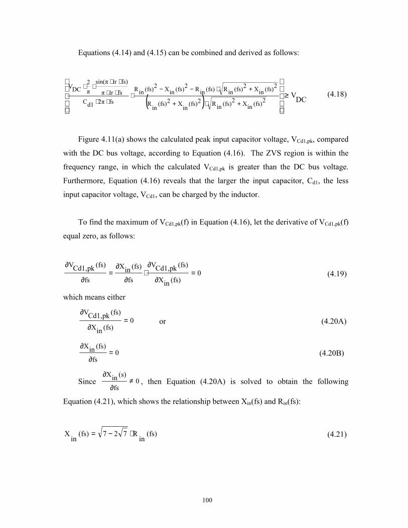
100
Equations (4.14) and (4.15) can be combined and derived as follows:
( ) DCV2(fs)inX2(fs)inR2(fs)inX2(fs)inR
2(fs)inX2(fs)inR(fs)inR2(fs)inX2(fs)inR
fs2πd1Cfstrπ
fs)trsin(ππ2
DCV≥
+⋅+
+⋅−−⋅
⋅⋅⋅⋅
⋅⋅⋅⋅
(4.18)
Figure 4.11(a) shows the calculated peak input capacitor voltage, VCd1,pk, compared
with the DC bus voltage, according to Equation (4.16). The ZVS region is within the
frequency range, in which the calculated VCd1,pk is greater than the DC bus voltage.
Furthermore, Equation (4.16) reveals that the larger the input capacitor, Cd1, the less
input capacitor voltage, VCd1, can be charged by the inductor.
To find the maximum of VCd1,pk(f) in Equation (4.16), let the derivative of VCd1,pk(f)
equal zero, as follows:
0(fs)inX
(fs)pkCd1,V
fs
(fs)inX
fs
(fs)pkCd1,V=
∂
∂⋅
∂
∂=
∂
∂(4.19)
which means either
0(fs)inX
(fs)pkCd1,V=
∂
∂or (4.20A)
0fs
(fs)inX=
∂
∂ (4.20B)
Since 0fs
(s)inX≠
∂
∂, then Equation (4.20A) is solved to obtain the following
Equation (4.21), which shows the relationship between Xin(fs) and Rin(fs):
(fs)in
R727(fs)in
X ⋅−= (4.21)

101
According to Equation (4.7), the phase θ(f) between the input voltage, Vin, and the
inductor current, iL, can be calculated, as shown in the following Equation (4.22), when
the maximal peak input capacitor voltage, VCd1,pk, is reached:
( ) o52.587271tan(fs)inR
(fs)inX1tanθ(fs) =−−=−=
(4.22)
Figure 4.11(b) shows that the maximum input capacitor voltage, Vcd1,pk,max, is
attained at the phase of the input impedance, Zin, which is equal to 52.58o. According to
Equations (4.16) and (4.22), the maximal peak charged/discharged voltage on the input
capacitor, Cd1, is expressed as shown in the following:
(fs)inRtr2fs3πd1C
fs)trsin(πDCV53.0
(fs)inR0.53
fsπ2d1Cfstrπ
fs)trsin(ππ2
DCVmax(fs)pkcd1,V
⋅⋅⋅⋅
⋅⋅⋅⋅=⋅
⋅⋅⋅⋅⋅⋅⋅⋅⋅
= (4.23)
where ( )
⋅⋅⋅⋅+⋅
+=2
LR2dCfsπ212NLR
R(fs)inR
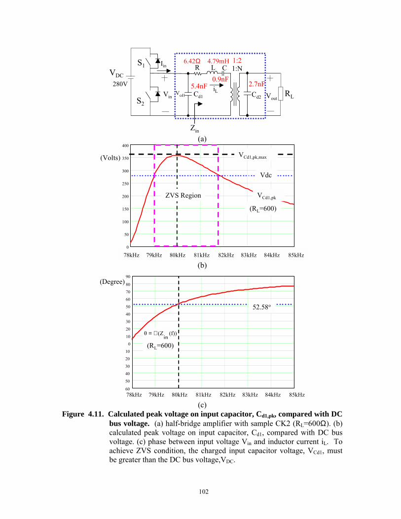
102
1:NR CL
Cd2Vin VoutCd1 RL
S1
S2
VDC
5.4nF 2.7nF0.9nF
1:24.79mH6.42Ω
280V
Iin
iLVcd1
Zin
(a)
0
50
100
150
200
250
300
350
400
Vdc
VCd1,pk
78kHz 79kHz 80kHz 81kHz 82kHz 83kHz 84kHz 85kHz
(Volts) VCd1,pk,max
(RL=600)
ZVS Region
(b)
60
50
40
30
20
10
0
10
20
30
40
50
60
70
80
90
78kHz 79kHz 80kHz 81kHz 82kHz 83kHz 84kHz 85kHz
(f))in
(Zθ ∠=
(Degree)
52.58o
(RL=600)
(c)Figure 4.11. Calculated peak voltage on input capacitor, Cd1,pk, compared with DC
bus voltage. (a) half-bridge amplifier with sample CK2 (RL=600Ω). (b)calculated peak voltage on input capacitor, Cd1, compared with DC busvoltage. (c) phase between input voltage Vin and inductor current iL. Toachieve ZVS condition, the charged input capacitor voltage, VCd1, mustbe greater than the DC bus voltage,VDC.

103
Condition 2: Minimizing Dead Time for ZVS Condition
In order to provide sufficient time for the inductor to charge/discharge the input
capacitor, Cd1, the dead time between the switching of the half-bridge switches, S1 and
S2, should be greater than one quarter of the resonant period for the serial resonating
loop among Cd1, L, C, Cd2 and RL. With a given load, RL, this serial resonant frequency,
fserial, of the serial resonating loop among Cd1, L, C, Cd2 and RL can be solved using
Equation (4.24), as shown in Equation (4.25):
⋅⋅+⋅⋅
⋅⋅++⋅=⋅
]2)LRd2Cr(ω1[d2C2N
2)LRd2Cr(ω
d1C1
C1
rω
1L
rω (4.24)
where serialf2πrω ⋅=
then
LRd2CNeqCL4π
]keqC2LRd2C2
LR2d2C2N2NeqCL[eqCL2
serialf⋅⋅⋅⋅⋅
+⋅⋅+⋅⋅+⋅⋅−⋅⋅⋅=
(4.25)
where2
LR
d2C2N2
eqCL22
LR2
d2C4N
eqCL24N2
eqC2Lk ⋅⋅⋅⋅⋅−⋅⋅⋅⋅⋅+⋅⋅=
2eq
C4L
R2d2
C2Neq
C4L
R3d2
C24L
R4d2
C4N ⋅⋅+⋅⋅⋅⋅+⋅⋅+
d1CCd1CC
eqC+
⋅= (4.26)
Therefore, the dead time for achieving ZVS condition can be calculated as the follows:
serial
serialtimedead f4
14
Tt
⋅=≥−
]keqC2LRd2C2
LR2d2C2N2NeqCL[eqCL2
LRd2CNeqCLπ
+⋅⋅+⋅⋅+⋅⋅−⋅⋅⋅
⋅⋅⋅⋅⋅= (4.27)

104
where
2L
Rd2
C2N2eq
CL22L
R2d2
C4Neq
CL24N2eq
C2Lk ⋅⋅⋅⋅⋅−⋅⋅⋅⋅⋅+⋅⋅=
d1CCd1CC
eqC+
⋅=

105
4.3.3 Minimizing Circulating Current for ZVS Condition
Figure 4.12 shows the waveforms of the input voltage and inductor current of the L-
C resonant tank driven by a half-bridge amplifier. This inductor current, iL, is dependent
on the switching frequency, fs, and the load resistance, RL. The amplitude of the
inductor current, iLpk, will be derived as follows in order to calculate the current stress on
the half-bridge switches, S1 and S2.
Since the piezoelectric transformer works as a band-pass filter, the magnitude of the
input voltage, Vin, applied to the input terminal of the L-C resonant tank at switching
frequency, fs, can be simplified and expressed as the fundamental component, shown in
the following:
π2
frtπ
f)rtsin(πDCV
sfffund,inV ⋅⋅⋅
⋅⋅⋅=
=(4.28)
where VDC is the DC bus voltage,
tr is the rising time of input voltage, Vin, and
fs is the switching frequency.
Therefore, the amplitude of the inductor current, iLpk, at switching frequency, fs, can
be expressed as shown in the following:
sffinZ
1π2
frtπ
f)rtsin(πDCV
sffinZ
sfflfundamentain,V
sffLpki
=
⋅⋅⋅⋅
⋅⋅⋅=
=
==
=
(4.29)
where sffinZ
= is the magnitude of the input impedance excluding the input
capacitor, Cd1.

106
If 51
Tstftr r
s ≈=⋅ , then the amplitude of the inductor current, iLpk, at switching
frequency, fs, can be plotted as shown in Figure 4.13.

107
1:NR CL
Cd2Vin VoutCd1 RL
S1
S2
VDC
Zin
iL
D1
D1
Iin
D2
(a)
Vin
iL
Li∆
tr
T
0iLpk
Time(b)
Figure 4.12. Input voltage waveform and inductor current waveforms of L-Cresonant tank. (a) half-bridge amplifier. (b) waveforms of inductorcurrent and input voltage.

108
1:NR CL
Cd2Vin VoutCd1 RL
S1
S2
VDC
5.4nF 2.7nF0.9nF
1:24.79mH6.42Ω
280V
Iin
iLVcd1
Zin
(a)
1
0.5
0
0.5
1
1.5
22
78kHz 79kHz 80kHz 81kHz 82kHz 83kHz 84kHz 85kHz
(Amp) )600L
(RpkLi Ω=
fs=81kHz
(b)
0
50
100
150
200
250
300
350
400
VDC
VCd1,pk(RL=600Ω)(Volt)
78kHz 79kHz 80kHz 81kHz 82kHz 83kHz 84kHz 85kHz
ZVS Region
(c)Figure 4.13. Amplitude of inductor current, iLpk, and peak input capacitor voltage,
VCd1,pk. (a) half-bridge amplifier with sample CK2. (b) amplitude ofinductor current. (c) magnitude of peak input capacitor voltage.

109
4.4 Matched Load for Optimal Efficiency
Besides the voltage gain and ZVS condition discussed in Sections 4.2 and 4.3, the
efficiency achieved while utilizing a radial vibration mode piezoelectric transformer for
electronic ballast applications remains to be evaluated in this section.
Since the loads of fluorescent lamps become resistive after ignition, fluorescent
lamps can simply be modeled resistive. In order to calculate the efficiency of
piezoelectric transformers, two dielectric loss components, Rcd1 and Rcd2, for the input
capacitor, Cd1, and the output capacitor, Cd2, respectively, need to be included in the
equivalent circuit of a piezoelectric transformer with the resistive load, RL, [A8] as
shown in Figure 4.14.
Cd1 Cd2
1:N+
Vin-
R L C
+Vout
-RLRcd2Rcd1
Zin
Figure 4.14. Piezoelectric transformer equivalent circuit model with dielectric losscomponents, Rcd1 and Rcd2.
These two dielectric loss components, Rcd1 and Rcd2, be calculated using the following
Equations (4.30) and (4.31) [A8]:
tanδd1
Cfsπ2
1cd1
R⋅⋅⋅⋅
= (4.30)
tanδd2
Cfsπ2
1cd2
R⋅⋅⋅⋅
= (4.31)
where δtan is the dielectric tangent of the piezoelectric material, and
fs is the switching frequency of the half-bridge switches.

110
Referring to Figure 4.15, the piezoelectric transformer model can be converted to a
series format, as shown in Figure 4.15(c) in order to conveniently calculate the
efficiency. With the resistive load, RL, the input power, output power and efficiency can
be derived as shown in Equations (4.32A), (4.32B) and (4.32C), respectively:
+++
++⋅=+⋅=
2)2
X1
(X2)2
R(R
2RR
cd1R
12in
V)in
Z1
cd1R
1(2
inVReinP
(4.32A)
2R1
2
)2X1j(X)2R(R2jX2R2
inVPout ⋅+++
+⋅= (4.32B)
==in
PoutP
Eff2R
1
)2R(Rcd1
R2)2X1(X)2
2X2
2(R
)2
2X2
2(Rcd1R⋅
+⋅++++
+⋅ (4.32C)
where
Csω
1L
sω1X
⋅−⋅= (4.33)
2q1
2q2Nd2Csω
1-2X
+⋅
⋅⋅= (4.34)
)2q(12N
1
cd2RLRcd2RLR
2R
+⋅⋅
+
⋅= (4.35)
cd2RLRcd2RLR
d2Csq+
⋅⋅⋅= ω (4.36)
fsπ2sω ⋅⋅=
fs is the switching frequency of the half-bridge switches.

111
To find the maximal efficiency in Equation (4.32C) with a given load RL, assume
its derivative, corresponding to X1, is equal to zero, as follows:
01X
Efffs1X
Efffs
=∂∂⋅
∂
∂=
∂∂ (4.37)
which means,
01X
Eff=
∂∂ , or (4.38A)
0fs1X=
∂
∂ (4.38B)
Since 0fs1X≠
∂
∂, then solve Equation (4.38A) to obtain
X1= -X2 (4.39)
Equation (4.39) means that
2q1
2q2Nd2Csω
1Csω
1Lsω +
⋅⋅⋅
=⋅
−⋅ (4.40)
where cd2
RLRcd2
RLRd2C
sωq
+
⋅⋅⋅=
Equation (4.40) shows that the maximal efficiency is achieved at the resonant
frequency with a specific resistive load, RL. This resonant frequency, fr, can be
calculated by the following:
eqRd2CNCL4π
]kC2eqRd2C2
eqR2d2C2N2NCL[CL2
fr⋅⋅⋅⋅⋅
+⋅⋅+⋅⋅+⋅⋅−⋅⋅⋅= (4.41)
where2
eqR
d2C2N2CL22
eqR2
d2C4NCL24N2C2Lk ⋅⋅⋅⋅⋅−⋅⋅⋅⋅⋅+⋅⋅=
2C4eq
R2d2
C2NC4eq
R3d2
C24eq
R4d2
C4N ⋅⋅+⋅⋅⋅⋅+⋅⋅+

112
Cd2CLRCd2RLR
eqR+
⋅= (4.42)
If Rcd2>>RL, then Req ≅ RL. According to Equations (4.30) and (4.31), the Rcd1 and
Rcd2 of sample CK2 at 81kHz are 91kΩ and 182kΩ, respectively, both of which are
much greater than RL=600Ω.
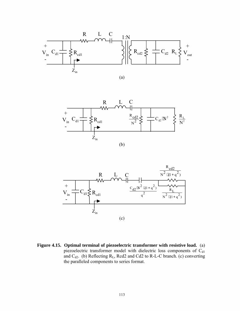
113
Cd1 Cd2
1:N+
Vin-
R L C
+Vout
-RLRcd2Rcd1
Zin
(a)
Cd1
+Vin-
R L C
Rcd1
Zin
2Ncd2R
2L
NR2
d2 NC ⋅
(b)
Cd1
+Vin-
R L C
Rcd1 )2q(12NLR
+⋅
)2q1(2Ncd2R
+⋅
2q
)2q(12Nd2C +⋅⋅
Zin
(c)
Figure 4.15. Optimal terminal of piezoelectric transformer with resistive load. (a)piezoelectric transformer model with dielectric loss components of Cd1and Cd2. (b) Reflecting RL, Rcd2 and Cd2 to R-L-C branch. (c) convertingthe paralleled components to series format.

114
In Figure 4.14, if the values of dielectric loss components, Rcd1 and Rcd2, are much
greater than R and RL, respectively, then these two dielectric loss components can be
ignored and removed from the equivalent circuit, as shown in Figure 4.16. Prior work
[A8] derived that the peak efficiency is attained when the load resistance equals the
matched load resistance, RL,max, at its corresponding resonant frequency, fr, for the
piezoelectric transformer model without the dielectric loss components, Rcd1 and Rcd2.
This matched load resistance, RL,max, can be calculated as follows:
d2matchL, Cfrπ2
1R⋅⋅⋅
= (4.43)
where fr is the corresponding resonant frequency with a given load RL.
According to the parameters of CK2, shown in Table 4.1, the curves of
efficiency vs. load resistance at the corresponding resonant frequencies can be plotted as
shown in Figure 4.17 for the piezoelectric transformer models with and without the
dielectric loss components, Rcd1 and Rcd2. Figure 4.17 shows that the peak efficiency
values of both models are achieved around the matched load resistance, RL,match
(=733Ω), at the corresponding resonant frequency.
Table 4.1. Measured parameters of equivalent circuit model for multi-layer radialvibration mode piezoelectric transformer sample CK2 (t1=t2=t3=80mils,D= 1180mils, n1=2, n2=1).
R L C Cd1 Cd2 N
LC
1fs =
Measured 6.42 Ω 4.79 mH 918.71 pF 5.41 nF 2.74 nF 2 75.86 kHz
Cd1 Cd2
1:N+
Vin-
R L C
+Vout
-RL
Zin
Figure 4.16. Piezoelectric transformer model without dielectric loss components.

115
Cd1 Cd2
1:N+
Vin-
R L C
+Vout
-RLRcd2Rcd1
Zin
(a)
Cd1 Cd2
1:N+
Vin-
R L C
+Vout
-RL
Zin
(b)
100 200 300 400 500 600 700 800 900 1000 11001200 1300 14001500 1600 17001800 1900 2000.7
0.75
0.8
0.85
0.9
0.95
1
100 500 1KΩ 1.5KΩ 2KΩ
733Ωd2Cfrπ2
1L,matchR =
⋅⋅⋅=
w/o Rcd1 and Rcd2
w/ Rcd1 and Rcd2
(c)
Figure 4.17. Efficiency vs. load resistance at corresponding resonant frequency forpiezoelectric transformer sample CK2. (a) equivalent circuit modelwith dielectric loss components, Rcd1 and R Cd2. (b) equivalent circuitmodel without dielectric loss components, RCd1 and RCd2. (c) efficiency vs.load resistance at corresponding resonant frequency. When RL is equal toRL,match, the efficiency is maximal.

116
4.5 Inductor-less Electronic Ballast
Based on the ZVS criteria, proposed in Section 4.3, this section presents a cost-
effective inductor-less piezoelectric transformer electronic ballast utilizing a radial
vibration mode piezoelectric transformer to drive a 4-foot 40-watt linear fluorescent
lamp at VDC=280V. At steady state, the equivalent on-resistance of this lamp is equal to
600Ω. According to the calculated efficiency curves, shown in Figure 4.18, the
efficiency with RL=600Ω at the corresponding resonant frequency is still very high and
is close to the efficiency peak. The radial vibration mode piezoelectric transformer
serves as a piezoelectric transformer resonant tank that replaces the conventional passive
L-C resonant tank. With its inherent piezoelectric resonant characteristics, the radial
vibration mode piezoelectric transformer is able to both ignite and provide sustaining
voltage to a linear fluorescent lamp. The operational principles, implementation and
experimental results of the proposed inductor-less piezoelectric transformer electronic
ballast circuit will be presented in this section.
100 200 300 400 500 600 700 800 900 1000 11001200 1300 14001500 1600 17001800 1900 2000.7
0.75
0.8
0.85
0.9
0.95
1
100 500 1KΩ 1.5KΩ 2KΩ
Ω600LR =
w/o Rcd1 and Rcd2
w/ Rcd1 and Rcd2
Figure 4.18. Efficiency vs. load resistance at corresponding resonant frequency forpiezoelectric transformer sample CK2.

117
4.5.1 Implementation of Prototype Circuit
According to the evaluation of voltage gain, ZVS condition and efficiency
discussed in Sections 4.2, 4.3 and 4.4, the radial vibration mode piezoelectric
transformer sample CK2 can be used for the electronic ballast to drive a 4-foot 40-watt
linear fluorescent lamp at VDC=280. Figure 4.19 shows both the voltage gain and the
peak input capacitor voltage, VCd1,pk, vs. frequency. Figure 4.20 shows both the
amplitude of the inductor current, iLpk, and the peak input capacitor voltage, Vcd1,pk, vs.
frequency. When the switching frequency is at 81kHz with VDC=280V, the
charged/discharged input capacitor voltage, VCd1, is greater than the DC bus voltage,
VDC, which means a ZVS condition can be achieved for the half-bridge switches, S1 and
S2. With RL=600Ω, the voltage gain is around 1(0dB), which is able to sustain the linear
fluorescent lamp.
Figure 4.21 shows the PSpice simulation results of the prototype circuit employing
the radial vibration mode piezoelectric transformer sample CK2. These results validate
the ZVS condition at switching frequency fs=81kHz. The schematic of the prototype
circuit for the proposed inductor-less piezoelectric transformer electronic ballast is
shown in Figure 4.22. This prototype circuit utilizes a voltage-controlled frequency
oscillator (VCO), CD4046, to generate a constant-frequency pulse signal to the gate
driver, L6384, which drives the half-bridge amplifier. The half-bridge switches, S1 and
S2, directly drives the radial vibration mode piezoelectric transformer (PT) without
requiring any magnetic device. This prototype circuit also has a voltage doubler for
universal-line applications. Figure 4.23 shows the completed prototype circuit for the
proposed inductor-less piezoelectric transformer electronic ballast.

118
1:NR CL
Cd2Vin VoutCd1 RL
S1
S2
VDC
5.4nF 2.7nF0.9nF
1:2
Piezoelectric Transformer
4.79mH6.42Ω
280V
(a)
0
50
100
150
200
250
300
350
400
VDC
VCd1,pk(RL=600)(Volt)
78kHz 79kHz 80kHz 81kHz 82kHz 83kHz 84kHz 85kHz
ZVS Region
(b)
0
1
2
3
78kHz 79kHz 80kHz 81kHz 82kHz 83kHz 84kHz 85kHz
Voltage Gain=
inV
outV
(RL=600)
11.1
inV
outV
>=
fs=81kHz
(c)
Figure 4.19. Peak input capacitor voltage, VCd1,pk, and voltage gain. (a) electronicballast with piezoelectric transformer sample CK2. (b) magnitude of peakinput capacitor voltage. (c) voltage gain. When the switching frequency isat 81kHz, the charged voltage, VCd1, on the input capacitor, Cd1, is greaterthan the DC bus voltage, which means the ZVS condition can be achievedfor the half-bridge switches, S1 and S2.

119
1:NR CL
Cd2Vin VoutCd1 RL
S1
S2
VDC
5.4nF 2.7nF0.9nF
1:2
Piezoelectric Transformer
4.79mH6.42Ω
280V
(a)
0
50
100
150
200
250
300
350
400
VDC
VCd1,pk(RL=600Ω)(Volt)
78kHz 79kHz 80kHz 81kHz 82kHz 83kHz 84kHz 85kHz
ZVS Region
(b)
1
0.5
0
0.5
1
78kHz 79kHz 80kHz 81kHz 82kHz 83kHz 84kHz 85kHz
(Amp) )600L
(RpkLi Ω=
fs=81kHz
(c)
Figure 4.20. Peak input capacitor voltage, VCd1,pk, and amplitude of inductorcurrent, iLpk. (a) electronic ballast with piezoelectric transformersample CK2. (b) magnitude of the peak input capacitor voltage. (c)amplitude of inductor current.

120
1:NR CL
Cd2Vin VoutCd1 RL
S1
S2
VDC
5.4nF 2.7nF0.9nF
1:2
Piezoelectric Transformer
4.79mH6.42Ω
280V
Iin
iL
(a)
iL
Iin
Vin
time
time
time0.001015 0.00102 0.001025 0.00103 0.001035200
0
200
400
0.001015 0.00102 0.001025 0.00103 0.0010351
0
1
0.001015 0.00102 0.001025 0.00103 0.0010351
0
1
time
(b)
Figure 4.21. PSpice simulation results of inductor-less piezoelectric transformerballast prototype circuit utilizing a radial vibration piezoelectrictransformer sample, CK2. (a) electronic ballast with piezoelectrictransformer sample CK2 (RL=600Ω). (b) simulated waveforms.

121
S1
S2 PTsw
L6384CD40462 Vcc
1 IN
3DT
87
6
5
4GND
LVG
OUT
HVGVBoot15
16
1112
R2
ZenerVDD
9 VCOin
VCOout
8Vss
6
7
VAC
CT
R1RDT
Load
S1
S2 PTsw
L6384CD40462 Vcc
1 IN
3DT
87
6
5
4GND
LVG
OUT
HVGVBoot15
16
1112
R2
ZenerVDD
9 VCOin
VCOout
8Vss
6
7
VAC
CT
R1RDT
Load
Figure 4.22. Detailed schematic of prototype circuit for proposed inductor-lesspiezoelectric transformer electronic ballast.
VoutVin
LinearFluorescent
Lamp (32W)S1
S2
Radial Vibration Mode Piezoelectric Transformer
VDC
VAC
Iin
(a)
(b)
Figure 4.23. Photo of completed prototype circuit for inductor-less piezoelectrictransformer ballast. (a) circuit block diagram. (b) photo of inductor-less piezoelectric transformer ballast. Without any magnetic device, theprototype circuit employs a radial vibration mode piezoelectrictransformer sample CK2 as a piezoelectric transformer resonant tank toignite and sustain a four-foot linear fluorescent lamp.
122
4.5.2 Experimental Results of Prototype Circuit
Without requiring any magnetic device, the prototype circuit utilizes a radial
vibration mode piezoelectric transformer as a piezoelectric transformer resonant tank to
ignite and sustain a linear fluorescent lamp. In Figure 4.24, this prototype circuit is
shown driving a 4-foot 40-watt linear fluorescent lamp, with output power of 32 watts,
without requiring any magnetic device. The efficiency of the whole prototype circuit
was around 90%, including control circuit, half-bridge, and the radial vibration mode
piezoelectric transformer. The experimental waveforms for the input voltage and
current of the on-board radial vibration mode piezoelectric transformer are shown in
Figure 4.25. The relationship shows the half-bridge switches, S1 and S2, working in a
ZVS condition. Figure 4.26 shows the input and output voltage waveforms. The input
voltage waveform of the radial vibration mode piezoelectric transformer shows no
voltage spikes and is characterized by slowly rising and falling slopes in order to create
less dv/dt on the half-bridge switches, S1 and S2. The parasitic input capacitor, Cd1, of
the radial vibration mode piezoelectric transformer performs as a turn-off snubber for
the half-bridge switches and yields this preferred switching characteristic.

123
VoutVin
LinearFluorescent
Lamp (32W)S1
S2
Radial Vibration Mode Piezoelectric Transformer
VDC
VAC
Iin
(a)
(b)
Figure 4.24. Photo of inductor-less piezoelectric transformer ballast driving a linearfluorescent lamp. (a) circuit block diagram. (b) after strike-on. Thisprototype circuit is driving a 4-foot 40-watt linear fluorescent lamp withoutrequiring any magnetic device. The output power was 32 watts.

124
VoutVin
LinearFluorescent
Lamp (32W)S1
S2
Radial Vibration Mode Piezoelectric Transformer
VDC
VAC
Iin
(a)
Iin(0.5A/Div)
Vin(100V/Div)
(b)
Figure 4.25. Experimental results of inductor-less piezoelectric transformer ballastprototype circuit. (a) circuit block diagram. (b) input voltage waveform(upper) and input current waveform (bottom). The input current andvoltage waveforms of the radial vibration mode piezoelectric transformershow the switches, S1 and S2, operate in a ZVS condition.

125
VoutVin
LinearFluorescent
Lamp (32W)S1
S2
Radial Vibration Mode Piezoelectric Transformer
VDC
VAC
Iin
(a)
Vin(100V/Div)
Vout(100V/Div)
(b)
Figure 4.26. Input voltage waveform and output voltage waveform of prototypecircuit utilizing a radial vibration mode piezoelectric transformersample, CK2. (a) circuit block diagram. (b) input voltage waveform(upper) and output voltage waveform (bottom).
126
4.6 Inductor-less Electronic Ballast Incorporating PFC Function
Presently, there are many input power factor regulations concerning lighting
products. The purpose of these regulations is to increase the operational efficiency of
power generators for electric power plants, and hence directly reduce the quantity of
natural resources used by electric power plants. In particular, fossil fuel energy sources
can affect pollutants and atmospheric contaminants, such as carbon dioxide, which
contribute to what is known as the greenhouse effect.
In order to meet power factor regulations, such as the IEC-61000, many charge
pump power factor correction (PFC) schemes have been well developed and studied for
use with electronic ballasts. These PFC schemes can be categorized into three major
types: voltage source, current source, and voltage source plus current source [C1-C11].
However, all these have been implemented with conventional magnetic devices.
This section will present the design and implementation of an inductor-less PFC
piezoelectric transformer ballast utilizing a radial vibration mode piezoelectric
transformer. Considering its simplicity and performance, this chapter will focus on
voltage source charge pump power factor correction (VS-CP-PFC) electronic ballast.
This chapter will design and develop an inductor-less VS-CP-PFC electronic ballast
utilizing a radial vibration mode piezoelectric transformer to drive a 40W white-light
linear fluorescent lamp, with an equivalent on-resistance equal to 350Ω, at VAC= 120V
and output power at 39W. The radial vibration mode piezoelectric transformer sample,
CK2, will first be evaluated for the application of the proposed inductor-less VS-CP-
PFC electronic ballast. Based on the ZVS criteria described in Section 4.3 and the
physics-based equivalent circuit model, derived in Chapter 2, a suitable radial vibration
mode piezoelectric transformer sample will be selected for the prototype circuit.

127
4.6.1 Voltage Source Charge Pump Power Factor Correction Electronic Ballast
By adding two diodes, Dx and Dy, and charge pump capacitor, Cp, to the electronic
ballast, as shown in Figure 4.27, the PFC function can be achieved by the VS-CP-PFC
electronic ballast [C9, C10]. The charge pump capacitor, Cp, is in series with a high-
frequency voltage source to pump energy from the AC line and discharge its stored
energy to the bulk capacitor, CB, in order to reach unity input power factor [C1]. The
minimal value of the charge pump capacitor, Cp, can be calculated by the following
equation [C1]:
2inVfsη
Pout2Cp⋅⋅
⋅= (4.44)
where Pout is the output power,
η is the efficiency,
fs is the switching frequency of the half-bridge switches, and
inV is the magnitude of the input AC voltage.
By replacing the L-C resonant tank, shown in Figure 4.28, with a piezoelectric
transformer, the inductor-less VS-CP-PFC piezoelectric transformer electronic ballast is
proposed, as shown in Figure 4.28.
This section will design and develop an inductor-less VS-CP-PFC electronic ballast
employing a radial vibration mode piezoelectric transformer to drive a 40W white-light
linear fluorescent lamp, with equivalent on-resistance equal to 350Ω, at VAC=120V and
output power at 39W.
According to Equation (4.37), the value of the charge pump capacitor, Cp, needs to
be greater than 33.4nF while the half-bridge switches operates at fs=81kHz. However,
the additional charge pump capacitor, Cp, paralleled with the input capacitor, Cd1, can
cause the half-bridge switches to lose ZVS condition because the inductor must then
charge/discharge the additional capacitor, Cp. Figure 4.29 shows that, if the additional

128
charge pump capacitor, Cp (=33.4nF) is paralleled with the input capacitor, Cd1, then the
charged/discharged voltage is below the required DC bus voltage, VDC=170V, which
leads to the loss of ZVS condition for the half-bridge switches, S1 and S2. Therefore, the
radial vibration mode piezoelectric transformer sample, CK2, cannot be used for the
proposed inductor-less VS-CP-PFC electronic ballast.
In order to assure that the half-bridge switches achieve ZVS condition, the next
section will utilize the physics-based equivalent circuit model of the radial vibration
mode piezoelectric transformer, developed in Chapter 2, to select a suitable radial
vibration mode piezoelectric transformer sample for implementation of the inductor-less
VS-CP-PFC electronic ballast.

129
VoutVin
S1
S2
VDCVAC
Iin R L C 1:N
Cd1Cd2
CB
(a)
Vout
S1
S2
VDCVACR L C 1:N
Cd1 Cd2
Cp
Dx Dy
Vin
CB
(b)
Figure 4.27. Voltage source charge pump power factor correction (VS-CP-PFC)electronic ballast [C9, C10]. (a) conventional electronic ballast. (b)VS-CP-PFC electronic ballast. With twoadditional diodes, Dx and Dy,and charge pump capacitor, Cp, the inductor-less electronic ballast can bemodified to have power factor correction function.

130
Vout
S1
S2
VDCVAC
Cp
Dx Dy
VinPiezoelectricTransformer
(a)
Vout
S1
S2
VDCVACR L C 1:N
Cd1 Cd2
Cp
Dx Dy
Vin
Piezoelectric TransformerEquivalent Circuit
(b)
Figure 4.28. Inductor-less voltage source charge pump power factor correct (VS-CP-PFC) piezoelectric transformer electronic ballast. (a) VS-CP-PFCballast utilizing a piezoelectric transformer. (b) VS-CP-PFC electronicballast with an equivalent circuit of piezoelectric transformer. This circuitincorporates the concept of conventional VS-CP-PFC electronic ballast toimplement inductor-less piezoelectric transformer electronic ballastfunction with power factor correction.

131
Vout
S1
S2
VDCVACR L C 1:N
Cd1Cd2
Cp
Dx Dy
Vin
Radial Vibration ModePiezoelectric Transformer
Sample, CK2
5.4nF 2.7nF
6.4Ω 4.79mH 0.9nF170VDC
(a)
0
50
100
150
200
250
300
(Volt)
78kHz78.5kHz 79kHz 80kHz78.5kHz 79.5kHz
VDC=170V
Cd1
Cd1+CP
(b)
Figure 4.29. Charged/discharged voltage, Vin, of input capacitor, Cd1, paralleledwith additional charge pump capacitor, Cp=33.4nF. (a) inductor-lessVS-CP-PFC electronic ballast with radial vibration mode piezoelectrictransformer sample CK2. (b) peak input capacitor voltage. Withadditional charge pump capacitor, Cp, paralleled with the input capacitor,Cd1, the charged/discharged voltage is far below the required DC busvoltage, VDC=170V, which leads to the loss of ZVS condition for thehalf-bridge switches, S1 and S2.

132
4.6.2 Design of Radial Vibration Mode Piezoelectric Transformer
According to the criteria for achieving ZVS condition, which was detailed in the
previous chapter, the peak input capacitor voltage, VCd1,pk, needs to be greater than or
equal to the DC bus voltage, VDC, before the turn-on of the half-bridge switch, S1/S2, as
shown in Figure 4.30. However, with the additional charge-pump capacitor Cp, the
actual input capacitor of the piezoelectric transformer becomes Cd1+Cp. Equation (4.23)
expresses the maximal peak input capacitor voltage, VCd1,pk, and can be rewritten to
include the additional charge-pump capacitor, Cp, as follows:
)Cpd1C((fs)inR1
rt2fs3π
fs)trsin(π0.53DCV
max(fs)pkCd1,V+⋅
⋅⋅⋅
⋅⋅⋅⋅= (4.45)
where tr is rising time of the charged voltage of input capacitor, Cd1,
fs is the switching frequency of the half-bridge switches S1 and S2, and
( ) ⋅⋅⋅⋅+⋅
+=2
LRd2Cfsπ212N
LRR(fs)inR (4.46)
Vout
S1
S2
VDCVACR L C 1:N
Cd1 Cd2
Cp
Dx Dy
Vin
Piezoelectric TransformerEquivalent Circuit
iL
Zin(f)=Rin(f)+jXin(f)
Figure 4.30. Half-bridge amplifier with equivalent circuit of piezoelectrictransformer.

133
Referring to Chapter 2, the resistor, R, and the input capacitor, Cd1, of the physics-
based equivalent circuit model for the radial vibration mode piezoelectric transformer
can be expressed as:
r21n
)2t2n1t1(n
231dQm32
3)1(3E
11Sρ2R
⋅
⋅+⋅⋅
⋅⋅
−⋅⋅⋅=
σ(4.47)
1t
E11
St33ε
231d
1t33ε
2rπ1n
d1C
⋅−⋅⋅⋅⋅
= (4.48)
When d2
L Cfπ21R⋅⋅⋅
≈ for maximal efficiency, then
2N2
LRR(f)
inR
⋅+≈ (4.49)
Therefore, Equation (4.45) can be approximated as
)2N
RLR(2)Cp
d1(Cr
t2fs3π
fs)trsin(πDC
V53.0
max(fs)
pkCd1,V
1
+⋅⋅+⋅
⋅⋅
⋅⋅⋅⋅≈ (4.50)
where 2
n1
nN = ,
n1 is the layer number of the primary side, and
n2 is the layer number of the secondary side.
Combining Equations (4.47), (4.48) and (4.50), the maximal voltage of the input
capacitor, Cd1, and can be rewritten as follows:
+
⋅
⋅+⋅⋅
⋅⋅
−⋅⋅⋅⋅⋅+
⋅−⋅⋅⋅⋅
⋅
⋅⋅
⋅⋅⋅⋅≈
2N
RL
r2
1n
)2
t2
n1
t1
(n
231
dQm32
3)1(3
E11
Sρ22Cp
1t
)E11
St33ε
231
d1(t
33ε2rπ
1n
1
rt
2f
3π
f)trsin(πDC
V53.0
max(fs)
pkCd1,V
σ
(4.51)

134
Referring to Equation (4.51), there are many possible ways to increase the maximal peak
input capacitor voltage, VCd1,pk, all of which are associated with the additional charge-
pump capacitor. Examples of these methods include:
(1) increasing 2
n1
nN =
(2) decreasing the radius, r,
(3) increasing the layer thickness, t1, of theprimary side, and
(4) decreasing the layer thickness, t2, of the secondary side.
With the same dimensions and piezoelectric ceramic material as were used in the
previous radial vibration mode piezoelectric transformer sample, CK2, a new sample,
CE1, can be obtained by adding two more layers on the primary side. Therefore,
Sample CE1 has four layers on the primary side and one layer on the secondary side,
with the same diameter and layer thickness as sample CK2, i.e. t1=t2=80mils and
diameter=1180mils. Table 4.2 shows the measured parameters of the equivalent circuit
model for five-layer radial vibration mode piezoelectric transformer samples, CK2 and
CE1. The measured turns ratio, N, of sample CE1 is 4.97, which is much higher than
that of sample CK1, in which N=2.
Table 4.2. Measured parameters of equivalent circuit model for five-layer radialvibration mode piezoelectric transformer samples, CK2 and CE1.
R L C Cd1 Cd2 N
LC
1fs =
CK2 6.42 Ω 4.79 mH 918.71 pF 5.41 nF 2.74 nF 2 75.86 kHz
CE1 2.13Ω 1.67mH 2.85nF 11.1nF 2.75nF 4.97 72.95kHz

135
Figure 4.31 shows the new five-layer radial vibration mode piezoelectric
transformer sample, CE1, has higher peak input capacitor voltage, VCd1,pk, than the
required DC bus voltage, VDC=170V, with an additional charge pump capacitor, Cp,
which leads to ZVS conditions for the half-bridge switches, S1 and S2.

136
Vout
S1
S2
VDCVACR L C 1:N
Cd1 Cd2
Cp
Dx Dy
Vin
Piezoelectric TransformerEquivalent Circuit
iL
Zin(f)=Rin(f)+jXin(f)
(a)
0
100
200
300
400
500
600
700
800
73.5kHz 74kHz 74.5kHz 75kHz
Cd1
Cd1+Cp
VDC=170V
VCd1,pk
ZVS Region
Volt
(b)
2
3
4
5
6
7
73.5kHz 74kHz 74.5kHz 75kHz
iL,pkZVS
Region
Amp
(c)
Figure 4.31. Charged/discharged voltage, Vin, on input capacitor Cd1 paralleledwith additional charge pump capacitor, Cp=33.4nF. (a) VS-CP-PFCelectronic ballast employing a radial vibration mode piezoelectrictransformer sample CE1. (b) peak input capacitor voltage. (c) amplitudeof inductor current.

137
4.6.3 Implementation and Experimental Results
Figure 4.32 shows the schematic of the developed inductor-less VS-CP-PFC
piezoelectric transformer electronic ballast utilizing the five-layer radial vibration mode
piezoelectric transformer sample, CE1. Figure 4.33 shows the experimental results of
the inductor-less VS-CP-PFC electronic ballast circuit with Vin=120Vrms, including
input current waveform, input voltage waveform, and input current harmonics. The
measured current harmonics are below the required boundary. The measured power
factor is 0.995 and the THD is 8.597%. However, the efficiency is only 72% due to the
large circulating current flowing through the half-bridge switches and diodes, and thus
reducing the efficiency of the circuit.
C p
S1
S2
D x D y
C B
vin va
Lam
p
ia
iin
voEMIFilter
Figure 4.32. Schematic of inductor-less VS-CP-PFC piezoelectric transformerballast utilizing five-layer radial vibration mode piezoelectrictransformer sample, CE1, (Vin=120VAC, Pout=38.8W, Cp=33.4nF). This five-layer sample has four layers at the primary side and one layeron the secondary side. The equivalent resistance of the lamp is 350Ω .

138
(a)
Input Current Harmonics
Required:
M easured:
Input Current Harmoincs35%
10%
20%
30%
25%
15%
5%
2 3 5 7 9 11 13 15(b)
Figure 4.33. Experimental results of VS-CP-PFC piezoelectric transformerelectronic ballast. (a) input voltage waveform (upper) and inputcurrent waveform (bottom). (b) measured and required input currentharmonics. The measured input current harmonics is far below therequirement, IEC61000.

139
4.7 Summary
This chapter has proposed ZVS criteria to evaluate the equivalent circuit of
piezoelectric transformers for ZVS condition in the electronic ballast application. The
purpose of ZVS criteria is to analyze the charged/discharged voltage across the input
capacitor of the piezoelectric transformer, as compared with the DC bus voltage. Based
on the proposed ZVS criteria, this chapter has presented inductor-less piezoelectric
transformer electronic ballast circuit utilizing suitable radial vibration mode
piezoelectric transformer samples without requiring any magnetic devices.
The developed inductor-less ballast prototype was used to drive a 4-foot 40-watt
linear fluorescent lamp with an output power of 32 watts. Since the switches of the
proposed circuit work in a ZVS condition, their turn-on switching losses can be
significantly reduced. In addition, the input capacitor of the radial vibration mode
piezoelectric transformer can be a useful turn-off snubber for the half-bridge switches in
order to reduce the turn-off voltage spike and to reduce the turn-off losses for the half-
bridge switches of the proposed circuit. Through these innovative circuit techniques, the
efficiency of the total proposed circuit can achieve a commendable level of around 90%.
Furthermore, the low-profile design of the radial vibration mode piezoelectric
transformer can minimize the total circuit packaging size of smaller lamp fixtures,
translating into possible cost reduction as well.
Incorporating the proposed ZVS criteria and the derived physics-based equivalent
circuit model of the radial vibration mode piezoelectric transformer, which was
presented in Chapter 2, a suitable five-layer radial vibration mode piezoelectric
transformer sample CE1 was selected for the implementation of an inductor-less VS-CP-
PFC piezoelectric transformer electronic ballast. The measured current harmonics of a
prototype using the 5-layer radial vibration mode piezoelectric transformer sample are
less than the maximum specified by the IEC61000. The measured power factor is 0.995
and the THD is 8.597%. However, the efficiency of this PFC prototype circuit is only

140
72% due to the large circulating current flowing through the half-bridge switches and
diodes, which subsequently reduces the efficiency of the entire circuit.

141
CHAPTER 5
CONCLUSION AND FUTURE WORK
Replacing conventional L-C resonant tanks with piezoelectric transformers reduces
the component count and cost of DC/DC converters and electronic ballasts for
fluorescent lamps. Furthermore, the low-profile design of piezoelectric transformers
minimizes the total packaging size for the application circuit, possibly translating into
additional cost reduction as well.
This dissertation has presented the characterization of the piezoelectric transformer
and has described its use in electronic ballasts for fluorescent lamps. The
characterization and model of the radial vibration mode piezoelectric transformer have
also been revealed.
The piezoelectric transformer, an electromechanical device, is a combination of
piezoelectric actuators on the primary side and piezoelectric transducers on the
secondary side. Both the actuator and transducer are made of piezoelectric elements,
which are composed of electrode plates and piezoelectric materials, such as barium
titanate-based ceramics. A piezoelectric element can work either in longitudinal
vibration mode or in transverse vibration mode at a corresponding resonant frequency.
In the longitudinal mode, the direction of the mechanical stress is parallel to the electric
or polarization direction at a corresponding resonant frequency. In the transverse mode,
the direction of the mechanical stress is perpendicular to the electric or polarization
direction at a corresponding resonant frequency.
Piezoelectric transformers can be categorized into three major types: Rosen,
thickness vibration mode and radial vibration mode. The Rosen transformer is a
combination of a transverse mode piezoelectric actuator on the primary side and a

142
longitudinal mode piezoelectric transducer on the secondary side. The thickness
vibration piezoelectric transformer is a combination of a longitudinal mode piezoelectric
actuator on the primary side and a longitudinal mode piezoelectric transducer on the
secondary side. The radial vibration mode transformer is a combination of a transverse
mode piezoelectric actuator on the primary side and a transverse mode piezoelectric
transducer on the secondary side. The applications for piezoelectric transformers
include use in DC/DC converters and in electronic ballasts for fluorescent lamps.
Based on the piezoelectric and wave equations, the physics-based equivalent circuit
model for the major vibration mode of piezoelectric transformers can be derived. The
physics-based equivalent circuit model, which is composed of a network of L-C
resonant tanks, can provide a good reference for the design and application of these
transformers. Therefore, a physics-based equivalent circuit model was derived for the
newly invented radial vibration mode piezoelectric transformer for the major radial
vibration mode.
The Y-parameter equivalent circuit model, provided by an HP4194A impedance
analyzer, can be used to characterize the parameters of the equivalent circuit of
piezoelectric transformers. Samples of radial vibration mode piezoelectric transformers
were characterized to verify the derived physics-based equivalent circuit model. The
comparison results showed that the circuit model is in good agreement with the
corresponding measured results of the piezoelectric transformer samples when the total
thickness is much less than the radius. Since this circuit model was derived for the
major radial vibration mode, other spurious vibration modes, such as thickness vibration
mode, were not considered. However, when the total thickness becomes equal to the
radius, the resonant frequency of the thickness vibration mode approaches that of the
major radial vibration mode, which causes the parameter deviation between the derived
physics-based equivalent circuit model and the characterized equivalent circuit of radial
vibration mode piezoelectric transformers.
143
Besides the major vibration mode, piezoelectric transformers have many spurious
vibration modes in other frequency ranges. These vibration modes can be characterized
with a multi-branch equivalent circuit model, composed of several single L-C resonant
tanks, for the design and simulation of application circuits operating in wide frequency
ranges rather than the major vibration mode. The prior multi-branch equivalent circuit
model can very precisely characterize the input admittance, but cannot characterize the
voltage gain with an acceptable deviation for the radial vibration mode piezoelectric
transformer. This improved multi-branch equivalent circuit model uses more detailed
networks to describe the voltage gain and phase for the different spurious vibration
modes of the radial vibration mode piezoelectric transformer. Therefore, compared to
the prior multi-branch equivalent circuit model, the proposed model can much more
accurately characterize the input admittance and voltage gain of the radial vibration
mode piezoelectric transformer.
In order to evaluate the equivalent circuit of piezoelectric transformers for
achieving ZVS condition, two ZVS criteria were presented to analyze the
charged/discharged voltage across the input capacitor of piezoelectric transformers.
Based on these two ZVS criteria, a suitable radial vibration mode piezoelectric
transformer sample can be evaluated and chosen for the implementation of inductor-less
piezoelectric transformer electronic ballast circuit. Associating the proposed ZVS
criteria and the derived physics-based equivalent circuit model of a radial vibration
mode piezoelectric transformer, a suitable radial vibration mode piezoelectric
transformer sample can be selected for the application of an inductor-less VS-CP-PFC
piezoelectric transformer electronic ballast. Furthermore, the proposed ZVS criteria also
can be used to evaluate and choose the suitable turn-off snubber capacitor for a general
half-bridge inverter driving an L-C resonant tank.
The developed prototype of the inductor-less piezoelectric transformer was used to
drive a four-foot 40-watt linear fluorescent lamp with an output power of 32 watts.
Since the switches of the proposed circuit work in ZVS condition, their turn-on
switching losses can be significantly reduced. In addition, the input capacitor of a radial

144
vibration mode piezoelectric transformer can be a useful turn-off snubber in order for the
half-bridge switches to lower the turn-off voltage spike and to reduce the turn-off losses
for the half-bridge switches of the proposed circuit. Through these innovative circuit
techniques, the efficiency of the total proposed circuit can achieve a commendable level
of around 90%.
By associating the proposed ZVS criteria and the derived physics-based equivalent
circuit model of radial vibration mode piezoelectric transformer, a suitable five-layer
radial vibration mode piezoelectric transformer sample, CE1, was selected for the
implementation of an inductor-less VS-CP-PFC piezoelectric transformer electronic
ballast. The measured current harmonics of a prototype using a 5-layer radial vibration
mode piezoelectric transformer sample are less than the IEC-61000 requirement,. The
measured power factor is 0.995 and the THD is 8.597%. However, the efficiency of this
PFC prototype circuit is only 72% due to the large circulating current flowing through
the half-bridge switches and the corresponding reduced efficiency of the circuit.
Recommended Future Work
The follows are some recommendations for future research work with the radial
vibration mode piezoelectric transformers.
• Advanced physics-based equivalent circuit:
To include the interaction effects of spurious vibration modes, such as thickness
vibration mode, for the physics-based equivalent circuit model of the radial vibration
mode piezoelectric transformer.
• More PFC applications:
To incorporate other existing PFC schemes by utilizing the radial vibration mode
piezoelectric transformers for electronic ballasts.
• Packaging:
To integrate radial vibration mode piezoelectric transformers with other electronic
components on PCB board.

145
• Thermal analysis:
To investigate the thermal model and the power dissipation capability of radial
vibration mode piezoelectric transformers.

146
REFERENCES
A. Piezoelectric Transformers
[A1] C. A. Rosen, US Patent No. 2,974,296, March 1961.
[A2] C. A. Rosen, Analysis and Design of Ceramic Transformer and Filter Elements,
Ph.D. Dissertation, Electrical Engineering Dept., Syracuse University, Aug. 1956.
[A3] C. A. Rosen, Ceramic Transformers and Filters, Proceedings of Electronic
Comp. Symp., 1956, pp. 205-211.
[A4] Y. Sasaki, K. Uehara and T. Inoue, “Piezoelectric Ceramic Transformer Being
Driven with Thickness Extensional Vibration, US Patent No. 5,241,236, Aug. 31,
1993.
[A5] R. P. Bishop, Multi-Layer Piezoelectric Transformer, US Patent No. 5,834,882,
Nov. 10, 1998.
[A6] S. W. Tehon, Piezoelectric and Magnetostrictive Transducers, Ph.D. Dissertation,
University of Illinois, Urbana, Illinois, 1958.
[A7] H. W. Katz, Solid State Magnetic and Dielectric Devices, John Wiley & Sons,
New York, 1959.
[A8] C. Y. Lin, Design and Analysis of Piezoelectric Transformer Converters, Ph.D.
Dissertation, Virginia Tech, July 1997.
[A9] T. Zaitsu, Power Conversion Using Piezoelectric Transformer, Ph.D. Dissertation,
Kyushu University, Fukuoka, Japan, Aug. 1997.
[A10] T. Ikeda, Fundamentals of Piezoelectricity, Oxford University Press, 1990.
[A11] IEEE Standard on Piezoelectricity, IEEE, 1978.

147
B. Piezoelectric Transformer Converters and Inverters
[B1] T. Zaitsu, T. Inoue, O. Ohnishi and A. Iwamoto, 2-MHz Power Converter with
Piezoelectric Ceramic Transformer, Proceedings of IEEE INTELEC92, pp. 430-
437.
[B2] T. Zaitsu, T. Inoue, O. Ohnishi and Y. Sasaki, 2-MHz Power Converter with
Piezoelectric Ceramic Transformer, IEICE Trans. Electron., Vol. E77-C, No. 2,
Feb. 1994, pp. 280-286.
[B3] O. Ohnishi, Y. Sasaki, T. Zaitsu, H. Kishie and T. Inoue, Piezoelectric Ceramic
Transformer for Power Supply Operating in Thickness Extensional Vibration
Mode, IEICE Trans. Fundamentals, Vol. E77-A, No. 12, Dec. 1994, pp. 2098-
2105.
[B4] T. Zaitsu, T. Ninomiya and M. Shoyama, Piezoelectric Transformer Converter
with PWM Control, IEICE Trans. Communication, Vol. E80-B, No. 7, July
1997, pp. 1035-1043.
[B5] T. Zaitsu, O. Ohnishi, T. Inoue, M. Shoyama, T. Ninomiya, Fred C. Lee and G.
Hua, Piezoelectric Transformer Operating in Thickness Extensional Vibration
and Its Application to Switching Converter, Proceedings of IEEE PESC94, pp.
585-589.
[B6] T. Zaitsu, Y. Fuda, Y. Okabe, T. Ninomiya, S. Hamamura and M. Katsuno, New
Piezoelectric Transformer Converter for AC-Adapter, Proceedings of IEEE
APEC97, pp. 568-572.
[B7] M. Shoyama, K. Horikoshi, T. Ninomiya, T. Zaitsu and Y. Sasaki, Operation
Analysis of the Push-Pull Piezoelectric Inverter, Proceedings of IEEE APEC97,
pp. 573-578.
[B8] M. Shoyama, K. Horikoshi, T. Ninomiya, T. Zaitsu and Y. Sasaki, Steady-State
Characteristics of the Push-Pull Piezoelectric Inverter, Proceedings of IEEE
PESC97, pp. 715-721.
[B9] T. Zaitsu, T. Shigehisa, T. Inoue, M. Shoyama and T. Ninomiya, Piezoelectric
Transformer Converter with Frequency Control, Proceedings of IEEE
INTELEC95, pp. 175-180.

148
[B10] T. Zaitsu, T. Shigehisa, M. Shoyama and T. Ninomiya, Piezoelectric
Transformer Converter with PWM Converter, Proceedings of IEEE APEC96,
pp. 279-283.
[B11] T. Zaitsu, T. Ninomiya, M. Shoyama and H. Tanaka, PWM-Controlled Current-
Mode Resonant Converter Using an Active-Clamp Technique, Proceedings of
IEEE PESC96, pp. 89-93.
[B12] H. Kakedhashi, T. Hidaka, T.Ninomiya, M. Shoyama, H. Ogasawara and Y. Ohta,
Electronic Ballast Using Piezoelectric Transformers for Fluorescent Lamps,
Proceedings of IEEE PESC98, pp. 29-35.
[B13] R. Bishop and C. Boyd, DC-AC Converter Circuit Using Resonating Multi-layer
Piezoelectric Transformer, US Patent No. 6,052,300, April 18, 2000.
[B14] R. L. Lin, F. C. Lee, E. M. Baker and D. Y. Chen, Inductor-Less Piezoelectric
Transformer Ballast Circuit, Proceedings of 16th Annual Research Symposium,
Virginia Tech, March 27, 2000, p. 40.
[B15] Ray L. Lin, Eric Baker, Jia Wei, Dan Chen and Fred C. Lee, Transoner
Characterization, Final Report, ELC-99-007, prepared for the Center for
Innovative Technology, Virginia, Jan. 31, 2000.
[B16] R. L. Lin, F. C. Lee, E. M. Baker and D. Y. Chen, Inductor-Less Piezoelectric
Transformer Ballast Circuit. Proceedings of Power Electronics Seminar at
Virginia Tech, September 19-21, 2000, pp. 309-314.
C. Power Factor Correction Ballast
[C1] Jinrong Qian, Advanced Single-Stage Power Factor Correction Techniques,
Ph.D. Dissertation, Virginia Tech, Sept. 1997.
[C2] M. H. Kheraluwala, R. L. Steigerwald and R. Gurumoorthy, A Fast Response
High Power Factor Converter with a Single Power Stage, IEEE PESC91, pp.
769-779.
[C3] M. Maechara, Inverter Device for Stable, High Power Factor Input Supply, US
Patent No. 5,274,540.

149
[C4] W. Chen, F. C. Lee and T. Yamauchi, Reduction of Voltage Stress in Charge
Pump Electronic Ballast, IEEE PESC96, pp. 887-893.
[C5] W. Chen, F. C. Lee and T. Yamauchi, An Improved Charge Pump Electronic
Ballast with Low THD and Low Crest Factor, IEEE APEC96, pp. 622-627.
[C6] J. Qian, F. C. Lee and T. Yamauchi, Analysis, Design and Experiments of a High
Power Factor Electronic Ballast, Proceedings of IEEE APEC97, pp.1023-1029,
1997.
[C7] J. Qian and F. C. Lee, Charge Pump High Power Factor Dimming Electronic
Ballast, Proceedings of IEEE PESC97, pp. 73-78.
[C8] J. Qian, F. C. Lee and T. Yamauchi, Current Source Charge Pump Power Factor
Correction Electronic Ballast, IEEE PESC97, pp. 67-72.
[C9] S. El-Hamamsy, M. Kheraluwala and D. Kachmarik, Multi-Resonant Boost High
Power Factor Circuit US Patent No. 5,488,269, Jan. 30, 1996.
[C10] S. El-Hamamsy, M. Kheraluwala and D. Kachmarik, Multi-Resonant Boost High
Power Factor Electronic Ballast for Compact Fluorescent Lamps, Proceedings
of IEEE PESC97, pp. 60-65.
[C11] Fengfeng Tao, Jinrong Qian and Fred C. Lee, A Comparative Study of a Family
of Charge Pump Power Factor Correction Electronic Ballasts, Proceedings of
APEC99, pp. 739745.
D. Miscellaneous
[D1] National Committee on Power Electronics, Report on Power Electronics and
Global competitiveness, ERI, 1992.
[D2] M. D. Levine, J. G. Koomey, L. Price, H. Geller and S. Nadel, Electricity End-
User Efficiency: Experience with Technologies, Market and Policies Through the
World, Energy, Vol. 20, No. 1, Jan. 1995, pp. 37-61.
[D3] Darnell Group Global Electronic Ballast Markets,
http://www.darnell.com/services/02-ballasts.stm.
[D4] Marc Schiler, Simplified Design of Building Lighting, John Wiley & Sons, Inc.,
New York, 1992.

150
[D5] MC14046B Data Sheet, Motorola Inc., 1997.
[D6] L6384 Data Sheet, STMicroelectronics, Dec. 1999.
[D7] APC 841-Lead Zirconate Titanate, http://www.americanpiezo.com, APC
International Ltd.
[D8] http://www.transoner.com.
[D9] PKI-802 Lead Zirconate Titanate,”
http://www.piezo-kinetics.com/navytype3.htm, Piezo Kinetics, Inc.
[D10] M. Kazimierczuk and D. Czarkowski, Resonant Power Converters, John Wiley &
Sons, Inc., 1995.

151
APPENDIX
Derivation of Physics-Based Equivalent Circuit Modelfor
Radial Vibration Mode Piezoelectric Transformer
The radial vibration mode piezoelectric transformer, as shown in Figure A.1, is
composed of two single-layer piezoelectric elements: a single-layer piezoelectric
actuator and a single-layer piezoelectric transducer both of which operate in transverse
mode. The behaviors of the actuator and transducer can be described as shown in the
following linear piezoelectric Equations (A1) and (A2).
Vin
VoutCeramic Layer
Ceramic Layer
rt2
t1
Figure A.1. Single-layer radial vibration mode piezoelectric transformer. Thisradial vibration mode piezoelectric transformer is composed of twosingle-layer piezoelectric elements: a single-layer piezoelectric actuatorand a single-layer piezoelectric transducer, both of which operate intransverse mode.
Piezoelectric Equations
Piezoelectric Actuator
⋅+⋅=
3E2E1E
33d23d13d32d22d12d31d21d11d
3T2T1T
E33SE
32SE31S
E23SE
22SE21S
E13SE
12SE11S
3S2S1S
and (A1)
Piezoelectric Transducer
⋅+⋅=
3E2E1E
T33
00
0T220
00T11
3T2T1T
33d32d31d23d22d21d13d12d11d
3D2D1D
ε
ε
ε
(A2)

152
where
S is mechanical strain,
T is mechanical stress,
E is electric field,
D is electric displacement,
d is piezoelectric constant,
sE is elastic compliance at constant electric field, and
εT is permittivity at constant stress.
Since both of the piezoelectric actuator and the piezoelectric transducer operate in
transverse mode, the piezoelectric transformer Equations (A1) and (A2), can be
simplified as shown Equations (A3) and (A4).
Piezoelectric Actuator in Transverse Mode
⋅+⋅=
3E00
33d31d0031d00
001T
E33SE
13SE13S
E13SE
11SE12S
E13SE
12SE11S
001S
00(A3)
Piezoelectric Transducer in Transverse Mode
⋅
+
⋅
=
3E00
T3300
0T220
00T11
001T
33d31d31d000000
3D00
ε
ε
ε
(A4)
The simplified linear piezoelectric Equations (A3) and (A4), are in the Cartesian-
coordinate system. However, the radial vibration mode piezoelectric transformer is
round, with its major vibration mode in the radial direction. Therefore, Equations (A3)
and (A4) need to be converted into the cylindrical-coordinate system with the following
transformation Equations (A5) to (A8). Following the derivation process, as shown in
Equations (A9) to (A12), the linear piezoelectric equation for the radial vibration mode
piezoelectric actuator can be simplified as shown in Equation (A13). Following the
derivation process, as shown in Equations (A14) to (A15), the linear piezoelectric

153
equation for the radial vibration mode piezoelectric transducer can be simplified as
shown in Equation (A16).
Transformation of Coordinates from Cartesian Coordinate System to CylindricalCoordinate System
Mechanical Strain
⋅
−
=
zSθSrS
100
02
1
2
1
02
1
2
1
3S2S1S
(A5)
Mechanical Stress
⋅
−
=
zTθTrT
100
02
1
2
1
02
1
2
1
3T2T1T
(A6)
Electric Field
⋅
−
=
zEθErE
100
02
1
2
1
02
1
2
1
3E2E1E
(A7)
Electric Displacement
⋅
−
=
zDθDrD
100
02
1
2
1
02
1
2
1
3D2D1D
(A8)

154
Radial Vibration Mode Piezoelectric Actuator
+⋅⋅=
zTθTrT
100
02
1
2
1
02
1-
2
1
E33SESES
ESESES
E13SE
12SE11S
100
02
1
2
1-
02
1
2
1
zSθSrS
1313
131112
⋅⋅
zEθErE
100
02
1
2
1
02
1-
2
1
33d0031d0031d00
100
02
1
2
1-
02
1
2
1
(A9)
Then,
⋅+⋅+⋅⋅
⋅−
⋅⋅+⋅⋅+⋅+
=
zE33dzTE33srTE
13s2θT)E
12sE11(s
zE31d2zTE13s2rT)E
12sE11(s
zSθSrS
(A10)
zE31d2zTE13s2rT)E
12sE11(srS ⋅⋅+⋅⋅+⋅+=⇒ (A11)
z31zE13r
E11 Ed2Ts2T)1(s ⋅⋅+⋅⋅+⋅−⋅= σ (A12)
where σ is the elastic compliance, and 11
21
ss
−=σ .
E11S
zTE13S2zE31d2rS
rT)1( ⋅−
⋅⋅−⋅⋅−=⇒
σ(A13)

155
Radial Vibration Mode Piezoelectric Transducer
+⋅⋅=
zTθTrT
100
02
1
2
1
02
1-
2
1
33d31d31d100
02
1
2
1-
02
1
2
1
zDθDrD
000000
⋅⋅
zEθErE
100
02
1
2
1
02
1-
2
1
T3300
0T220
00T11
100
02
1
2
1-
02
1
2
1
ε
ε
ε
(A14)
Then,
⋅+⋅+⋅⋅
+⋅+−⋅
−⋅−+⋅
=
zET33εzT33d31drT2
)T22ε
T11(ε
2θE
)T22ε
T11(ε
2rE
)T22ε
T11(ε
2θE
)T22ε
T11(ε
2rE
zDθDrD
(A15)
zET33εzT33drT31d2zD ⋅+⋅+⋅⋅=⇒ (A16)

156
Based on the simplified piezoelectric Equations (A13) and (A16), the current, I,
flowing through the electrode plates of the radial pizoelectric element, shown in Figure
A2, can be derived as shown in the following Equations (A17) to (A26).
tTPV
I
Figure A2. Transverse mode piezoelectric element.
rdrr ⋅⋅∫ ∫ ⋅=⋅== π0 2zDdt
ddSD
dt
dQ
dt
dI (A17)
rdrr
dt
d⋅⋅++⋅∫⋅⋅= )zET
33zT33drT31d0
2(2 επ (A18)
rdrdr
dt
d⋅⋅++
⋅−
⋅⋅−⋅⋅⋅⋅∫⋅⋅= ]zET
33zT33d)E11S)1(
zTE13S2zE312-rS
(31d0
2[2 εσ
π (A19)
rdrdr
dtd
⋅⋅⋅+⋅+⋅−
⋅⋅⋅−⋅⋅∫ ⋅⋅⋅= ]zET
332zT33d2)E11S)1(
zTE13S31d2zE2
312-31drS(
022[ ε
σπ (A20)
rdrdr
dtd
⋅⋅⋅+⋅+⋅−
⋅⋅⋅−
⋅−
⋅⋅−
⋅−
⋅⋅∫⋅= ]zET
332zT33d2E11S)1(
zTE13S31d2
E11S)1(
zE2312
E11S)1(
31drS22
0[ ε
σσσπ (A21)
+⋅⋅∫⋅−
⋅−⋅⋅∫ +⋅⋅⋅
⋅−
⋅⋅= rdr
r
dt
drrdr
dt
dzT)
0 E11S)1(
E13S31d
33(d20 31drSE
11S)1(
22
σπ
σ
π
zE)]T33
E11S
2311(T
332
22[
)1(⋅
⋅−⋅⋅⋅
⋅− εεπω
σ
drj (A22)
+⋅⋅∫⋅
−⋅⋅+⋅⋅⋅⋅⋅
=⋅−⋅−
rdrr
dt
drrdt
dzT)
0 E11S
E13S31d
33(d2)2
2S(E
11S
31d22
)1()1( σσπ
π
zE)]T33
E11S
2311(T
332[
)1(⋅
⋅−⋅⋅⋅⋅
⋅− εεπω
σ
drj (A23)

157
+⋅⋅∫⋅−
⋅−⋅⋅+⋅⋅
⋅−
⋅⋅⋅⋅= rdrzT)
r
0 E11Sσ)(1
E13S31d
33(d2dt
dπ
ru
dt
dE
11Sσ)(1
31drπ22
tV
)]T33ε
E11Sσ)(1
231d
(1T33ε
2r[πjω ⋅⋅⋅−
−⋅⋅ (A24)
t
V)]T
33E
11Sσ)(1
2311(T
332[E
11Sσ)(1
31d22⋅
⋅⋅−−⋅⋅+⋅
⋅−
⋅⋅⋅⋅=
εεπω
π drjv
r(A25)
VdmC ⋅⋅+⋅= ωψ jv (A26)
where
E11Sσ)(1
31d22
⋅−
⋅⋅⋅⋅=
rπψ (A27)
)T33
E11Sσ)(1
2311(T
33t
2rπdmC
εε
⋅⋅−−
⋅=
d(A28)
Based on the simplified piezoelectric Equations (A13) and (A16), the mechanical
vibration force, Fr, of the radial pizoelectric element can be derived as shown in the
following Equations (A29) to (A36).
tr2πrTArTrF ⋅⋅⋅=⋅= (A29)
Then,
tr2πE11Sσ)(1
zTE13S2zE31d2rS
rF ⋅⋅⋅⋅−
⋅⋅−⋅⋅−= (A30)
)zE31d2rS(E11Sσ)(1
trπ2⋅⋅−⋅
⋅−
⋅⋅⋅= (A31)
]zEE11Sσ)(1
31d2E
11Sσ)(1
1[trπ2 ⋅
⋅−
⋅−
∂
∂⋅
⋅−⋅⋅⋅⋅=
rru
(A32)
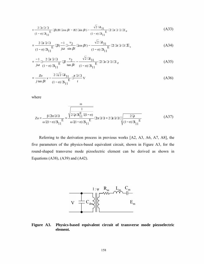
158
zEtrπ2E11Sσ)(1
31d2)sin2cos1(E
11Sσ)(1
trπ2⋅⋅⋅⋅⋅
⋅−
⋅−⋅−⋅⋅
⋅−
⋅⋅⋅= ll βββ BB (A33)
zEtrπ2E11Sσ)(1
31d2)cos
sin21
(E11Sσ)(1
trπ2⋅⋅⋅⋅⋅
⋅−
⋅−⋅⋅
−⋅
⋅−
⋅⋅⋅= l
lβ
βωβ
v
j(A34)
zEtrπ2E11Sσ)(1
31d2
tan2
E11Sσ)(1
trπ21⋅⋅⋅⋅⋅
⋅−
⋅−⋅
⋅−
⋅⋅⋅⋅
−=
lββ
ω
v
j(A35)
Vtrπ
E11Sσ)(1
31d22
tan tv
j
Zo ⋅⋅⋅
⋅−
⋅⋅−=
lβ(A36)
where
E11Sσ)(1
ρ2trπ2tr2πE11Sσ)(1ω
σ)(1E11Sρ2
1ω
E11Sσ)(1ω
tr2πβZo⋅−
⋅⋅⋅⋅⋅=⋅⋅⋅
⋅−⋅
−⋅⋅⋅≈
⋅−⋅
⋅⋅⋅= (A37)
Referring to the derivation process in previous works [A2, A3, A6, A7, A8], the
five parameters of the physics-based equivalent circuit, shown in Figure A3, for the
round-shaped transverse mode pizoelectric element can be derived as shown in
Equations (A38), (A39) and (A42).
Rm1 Lm1 Cm1
+
Vin_
d1C
1ψ:1
V Em
Rm Lm Cm
Cdm
ψ:1
Figure A3. Physics-based equivalent circuit of transverse mode piezoelectricelement.

159
σ)(1E11S
ρ2
mQ4tr2π
mQ8oZπ
mR−⋅
⋅⋅
⋅⋅⋅
=⋅
⋅= (A38)
2ρt2rπ
of1
σ)(1E11S
ρ28
trπ
oω8oZπ
mL⋅⋅⋅
=⋅−⋅
⋅⋅
⋅⋅=
⋅
⋅= (A39)
where
oo fπ2 ⋅⋅=ω (A40)
)1(E11Sρ2
1r2
1of
σ−⋅⋅⋅⋅
⋅= (A41)
t3π
E11S σ)(14
mL2oω
1m
C⋅
⋅−⋅=
⋅= (A42)
From Equations (A27) and (A28), the turns ratio and input capacitor are as follows:
E11Sσ)(1
31d22
⋅−
⋅⋅⋅⋅=
rπψ and (A43)
]T33ε
E11Sσ)(1
231d
[1T33εt
2rπdmC
⋅⋅−−
⋅= (A44)

160
VITA
The author was born in Taipei, Taiwan, in 1963. He received his B.S. and M.S.
degrees, both in electrical engineering, from Tatung University (formerly Tatung
Institute of Technology), Taipei, Taiwan, in 1986 and 1988, respectively.
From October 1988 to October 1994, he was employed by the Chung-Shan Institute
of Science and Technology, Department of Defense, Taiwan, as a research and
development specialist working to design and develop servo actuator control systems,
including servo motor control systems and servo hydraulic control systems.
In January 1995, he enrolled as a doctoral student in the Bradley Department of
Electrical and Computer Engineering at Virginia Polytechnic Institute and State
University, and became a member of the Virginia Power Electronics Center and the
Center for Power Electronics Systems.
In May 2000, he was employed by GE Lighting, Cleveland, Ohio, as an electronics
design engineer working to design and develop cost-effective high-performance
electronic ballasts for HID and fluorescent lamps.
He is a licensed Professional Engineer in the Commonwealth of Virginia. He is a
member of the Power Electronics Society and the Industry Electronics Society, IEEE.
His main research interests include power converters, power factor correction, soft-
switching technique, motor drives, motor design, piezoelectric transformer applications,
and electronic ballast.
The author can be contacted at: [email protected]