PI3PCIE2612-A - Diodes Incorporated SEL I SEL controls the mux through a flow-through latch. 3.6V...
18
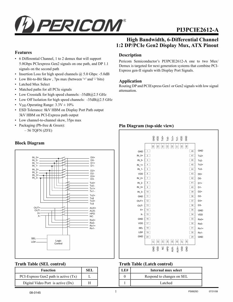
1 PS8925D 07/31/08 08-0145 Features • 6 Differential Channel, 1 to 2 demux that will support 5.0Gbps PCIexpress Gen2 signals on one path, and DP 1.1 signals on the second path • Insertion Loss for high speed channels @ 5.0 Gbps: -5.0dB • Low Bit-to-Bit Skew , 7ps max (between '+' and '-' bits) • Latched Mux Select • Matched paths for all PCIe signals • Low Crosstalk for high speed channels: [email protected] GHz • Low Off Isolation for high speed channels: [email protected] GHz • V DD Operating Range: 3.3V ± 10% • ESD Tolerance: 8kV HBM on Display Port Path output 3kV HBM on PCI-Express path output • Low channel-to-channel skew, 35ps max • Packaging (Pb-free & Green): – 56 TQFN (ZFE) Description Pericom Semiconductor’s PI3PCIE2612-A one to two Mux/ Demux is targeted for next generation systems that combine PCI- Express gen-II signals with Display Port Signals. Application Routing DP and PCIExpress Gen1 or Gen2 signals with low signal attenuation. Block Diagram Pin Diagram (top-side view) PI3PCIE2612-A High Bandwidth, 6-Differential Channel 1:2 DP/PCIe Gen2 Display Mux, ATX Pinout Truth Table (SEL control) Function SEL PCI-Express Gen2 path is active (Tx) L Digital Video Port is active (Dx) H Truth Table (Latch control) LE# Internal mux select 0 Respond to changes on SEL 1 Latched IN_0+ IN_0 IN_1+ IN_1 IN_2+ IN_2- IN_3+ IN_3- OUT+ OUT - X+ X- D0+ D0- D1+ D1- Tx0+ Tx0- Tx1+ Tx1 - D2+ D2- D3+ D3- Tx2+ Tx2 - Tx3+ Tx3 - LE# - - Logic Control SEL AUX+ AUX- HPD NC Rx0+ Rx0- Rx1+ Rx1-
Transcript of PI3PCIE2612-A - Diodes Incorporated SEL I SEL controls the mux through a flow-through latch. 3.6V...
1 PS8925D 07/31/0808-0145
Features• 6 Differential Channel, 1 to 2 demux that will support 5.0Gbps PCIexpress Gen2 signals on one path, and DP 1.1 signals on the second path• Insertion Loss for high speed channels @ 5.0 Gbps: -5.0dB• Low Bit-to-Bit Skew , 7ps max (between '+' and '-' bits)• Latched Mux Select• Matched paths for all PCIe signals• Low Crosstalk for high speed channels: [email protected] GHz• Low Off Isolation for high speed channels: [email protected] GHz• VDD Operating Range: 3.3V ± 10% • ESD Tolerance: 8kV HBM on Display Port Path output 3kV HBM on PCI-Express path output• Low channel-to-channel skew, 35ps max• Packaging (Pb-free & Green): – 56 TQFN (ZFE)
DescriptionPericom Semiconductor’s PI3PCIE2612-A one to two Mux/Demux is targeted for next generation systems that combine PCI-Express gen-II signals with Display Port Signals. Application Routing DP and PCIExpress Gen1 or Gen2 signals with low signal attenuation.
Block Diagram
Pin Diagram (top-side view)
PI3PCIE2612-AHigh Bandwidth, 6-Differential Channel
1:2 DP/PCIe Gen2 Display Mux, ATX Pinout
Truth Table (SEL control)Function SEL
PCI-Express Gen2 path is active (Tx) L
Digital Video Port is active (Dx) H
Truth Table (Latch control)LE# Internal mux select
0 Respond to changes on SEL
1 Latched
IN_0+IN_0IN_1+IN_1IN_2+IN_2-IN_3+IN_3-
OUT+OUT -
X+X-
D0+D0-D1+D1-
Tx0+Tx0-Tx1+Tx1 -
D2+D2-D3+D3-
Tx2+Tx2-Tx3+Tx3-
LE#
-
-
LogicControl
SEL
AUX+AUX-HPDNCRx0+Rx0-Rx1+Rx1-

2 PS8925D 07/31/08
PI3PCIE2612-AHigh Bandwidth, 6-Differential Channel
1:2 DP/PCIe Gen2 Display Mux, ATX Pinout
08-0145
Application Example
GMCHDP/TMDS/PCIe genII
x4
HPD / PEG RXPEG
Aux / PEG RX
x12 Tx
x14 Rx
PEG RX
PEG RX
x2
x2
x16 PEG Connector
DP Path willsupport 2.7 Gbps
Path willsupport Gbps
PCIe5
DP/PCIe2.0 (1:2) MuxPI3PCIE2612-A
Dx
HPD
AUX
Rx Rx Tx
IN
Pin DescriptionPin Number Pin Name Type Description26 AUX+ O Differential input from HDMI/DP connector. AUX+ makes a dif-
ferential pair with AUX-. AUX+ is passed through to the OUT+ pin when SEL = 1.
25 AUX- O Differential input from HDMI/DP connector. AUX- makes a dif-ferential pair with AUX+. AUX- is passed through to the OUT- pin when SEL = 1.
43, 42 D0+, D0- O Analog “pass through” output#1 corresponding to IN_0+ and IN_0-, when SEL = 1.
41, 40 D1+, D1- O Analog “pass through” output#1 corresponding to IN_1+ and IN_1-, when SEL = 1.
39, 38 D2+, D2- O Analog “pass through” output#1 corresponding to IN_2+ and IN_2-, when SEL = 1.
37, 36 D3+, D3- O Analog “pass through” output#1 corresponding to IN_3+ and IN_3-, when SEL = 1.

3 PS8925D 07/31/08
PI3PCIE2612-AHigh Bandwidth, 6-Differential Channel
1:2 DP/PCIe Gen2 Display Mux, ATX Pinout
08-0145
Pin Number Pin Name Type Description1, 11, 16, 20, 21, 28, 29, 35, 48, 49, 56
GND Power - Ground.
24 HPD I The HPD signal comes from the HDMI or DP connector. This is a low frequency, 0V to 5V (HDMI) or 3.6V (DP) input signal at the connector. The HPD input at the mux is 3.6V max, so HDMI HPD must be shifted down from 5V before it is passed to the mux.
2 IN_0+ I Differential input from GMCH PCIE outputs. IN_0+ makes a differential pair with IN_0-.
3 IN_0- I Differential input from GMCH PCIE outputs. IN_0- makes a dif-ferential pair with IN_0+.
4 IN_1+ I Differential input from GMCH PCIE outputs. IN_1+ makes a differential pair with IN_1-.
5 IN_1- I Differential input from GMCH PCIE outputs. IN_1- makes a dif-ferential pair with IN_1+.
7 IN_2+ I Differential input from GMCH PCIE outputs. IN_2+ makes a differential pair with IN_2-.
8 IN_2- I Differential input from GMCH PCIE outputs. IN_2- makes a dif-ferential pair with IN_2+.
9 IN_3+ I Differential input from GMCH PCIE outputs. IN_3+ makes a differential pair with IN_3-.
10 IN_3- I Differential input from GMCH PCIE outputs. IN_3- makes a dif-ferential pair with IN_3+.
19 LE# I The latch gate is controlled by LE. 3.6V tolerant, low-voltage, single-ended input.
23 NC Do Not Connect
12 OUT+ O Pass-through output from AUX+ input when SEL = 1. Pass-through output from Rx0+ input when SEL = 0.
13 OUT- O Pass-through output from AUX- input when SEL = 1. Pass-through output from Rx0- input when SEL = 0.
33 Rx0+ I/O Differential input from PCIE connector or device. Rx0+ makes a differential pair with Rx0-. Rx0+ is passed through to the OUT+ pin when SEL = 0.
32 Rx0- I/O Differential input from PCIE connector or device. Rx0- makes a differential pair with Rx0+. Rx0- is passed through to the OUT- pin when SEL = 0.
31 Rx1+ I Differential input from PCIE connector or device. Rx1+ makes a differential pair with Rx1-. Rx1+ is passed through to the X+ pin when SEL = 0.
(Continued)

4 PS8925D 07/31/08
PI3PCIE2612-AHigh Bandwidth, 6-Differential Channel
1:2 DP/PCIe Gen2 Display Mux, ATX Pinout
08-0145
Pin Number Pin Name Type Description30 Rx1- I Differential input from PCIE connector or device. Rx1- makes a
differential pair with Rx1+. Rx1- is passed through to the X- pin on a path that matches the Rx1+ to X+ path.
18 SEL I SEL controls the mux through a flow-through latch. 3.6V toller-ant low-voltage single-ended outputSEL = 0 for PCIE Mode SEL = 1 for DP Mode
54, 53 Tx0+,Tx0- O Analog “pass through” output#2 corresponding to IN_0+ and IN_0-, when SEL = 0.
52, 51 Tx1+, Tx1- O Analog “pass through” output#2 corresponding to IN_1+ and IN_1-, when SEL = 0.
47, 46 Tx2+, Tx2- O Analog “pass through” output#2 corresponding to IN_2+ and IN_2-, when SEL = 0.
45, 44 Tx3+, Tx3- O Analog “pass through” output#2 corresponding to IN_3+ and IN_3-, when SEL = 0.
6, 17, 22, 27, 34, 50, 55
VDD Power 3.3V DC Supply, 3.3V +/- 10%
14 X+ I/O HPD: Low frequency, 0V to 5V/3.3V (nominal) input signal at the connector. This signal comes from the HDMI/DP connector. X+: Analog “pass through” output corresponding to Rx1+.
15 X- I X- is an analog “pass-through” output corresponding to the Rx1- input. The path from Rx1- to X- must be matched with the path from Rx1+ to X+. X+ and X- form a differential pair when the pass-through mux mode is selected.

5 PS8925D 07/31/08
PI3PCIE2612-AHigh Bandwidth, 6-Differential Channel
1:2 DP/PCIe Gen2 Display Mux, ATX Pinout
08-0145
Recommended Operating ConditionsSymbol Parameter Conditions Min Typ Max Units
VDD 3.3V Power Supply 3.0 3.3 3.6 V
IDD Total current from VDD 3.3V supply
0 2.5 mA
TCASE Case temperature range for operation within spec.
-40 85 Celcius
Electrical Characteristics
Storage Temperature ....................................................–65°C to +150°CSupply Voltage to Ground Potential ................................–0.5V to +4.6VDC Input Voltage .............................................................. –0.5V to VDDDC Output Current .......................................................................120mAPower Dissipation ........................................................................... 0.5W
Note: Stresses greater than those listed under MAXIMUM RATINGS may cause permanent damage to the device. This is a stress rating only and functional operation of the device at these or any other conditions above those indicated in the operational sections of this specification is not implied. Expo-sure to absolute maximum rating conditions for extended periods may affect reliability.
Maximum Ratings(Above which useful life may be impaired. For user guidelines, not tested.)
DC Electrical Characteristics (TA = –40°C to +85°C, VDD = 3.3V ± 10%)Parameter Description Test Conditions Min Typ(1) Max Units
VIH-EN(2) Input high level 2.0 3.6 V
VIL-EN(2) Input Low Level 0 0.8 V
IIN_EN(2) Input Leakage Current Measured with input at VIH-EN max and VIL-EN min
–10 10 uA
RON On Resistance VDD = Min., VIN = 1.3V, IIN = 40mA 10 Ohm
CON On Channel Capacitance VIN = 0, VDD = 3.3V 3.0 pFNote:1. Typical values are at VDD = 3.3V, TA = 25°C ambient and maximum loading.2. For SEL and LE# inputs

6 PS8925D 07/31/08
PI3PCIE2612-AHigh Bandwidth, 6-Differential Channel
1:2 DP/PCIe Gen2 Display Mux, ATX Pinout
08-0145
Switching Characteristics (TA= -40º to +85ºC, VDD = 3.3V±10%)Parameter Description Test Conditions Min. Typ. Max. Units
tPZH, tPZLLine Enable Time - SEL to DX±, TXY±, RXY±, AUX±, HPD
See "Test Circuit for Electrical Chatacteristics"
0.5 12.0 ns
tPHZ, tPLZLine Disable Time - SEL to DX±, TXY±, RXY±, AUX±, HPD
See "Test Circuit for Electrical Chatacteristics"
0.5 12.0 ns
tb-b Bit-to-bit skew within the same differential pair
See "Test Circuit for Electrical Chatacteristics"
7 ps
tch-ch Channel-to-channel skew See "Test Circuit for Electrical Chatacteristics"
35 ps
Dynamic Electrical Characteristics for IN_x+/-, Rxy+/-, and Txy+/-Parameter Description Test Conditions Min. Typ.(1) Max. Units
DDIL Differential Insertion Loss
f=1.2GHzf=2.5GHzf=5.0GHzf=7.5GHz
-1.5-2.0-5.0-9.0
dBDDILOFF Differential Off Isolation f= 0 to 3.0GHz
f= 5.0GHz-23.0-20.0
DDRL Differential Return Lossf= 0 to 2.8GHzf= 2.8 to 5.0GHzf= 5.0 to 7.5GHz
-14.0-8.0-4.0
DDNEXT Near End Crosstalkf= 0 to 2.5GHzf= 2.5 to 5.0GHzf= 5.0 to 7.5GHz
-32.0-26.0-20.0
Dynamic Electrical Characteristics for Dx+/-Parameter Description Test Conditions Min. Typ.(1) Max. Units
DDILDP Display Port Differential Insertion Loss f= 0 to 1.35GHzf= 1.35 to 2.7GHz
-1.5-4.5
dBDDRLDP Display Port Differential Return Loss f= 0 to 2.7GHz -14
DDNEXT-DP
Display Port Near End Crosstalk f= 0 to 2.7GHz -32.0

7 PS8925D 07/31/08
PI3PCIE2612-AHigh Bandwidth, 6-Differential Channel
1:2 DP/PCIe Gen2 Display Mux, ATX Pinout
08-0145
Differential Insertion Loss
Differential Return Loss

8 PS8925D 07/31/08
PI3PCIE2612-AHigh Bandwidth, 6-Differential Channel
1:2 DP/PCIe Gen2 Display Mux, ATX Pinout
08-0145
Off Isolation
Crosstalk

9 PS8925D 07/31/08
PI3PCIE2612-AHigh Bandwidth, 6-Differential Channel
1:2 DP/PCIe Gen2 Display Mux, ATX Pinout
08-0145
Tx Eye Diagram, 5.0 Gbps
Dx Eye Diagram, 2.7 Gbps

10 PS8925D 07/31/08
PI3PCIE2612-AHigh Bandwidth, 6-Differential Channel
1:2 DP/PCIe Gen2 Display Mux, ATX Pinout
08-0145
Test Circuit
Test Circuit
Test Circuit

11 PS8925D 07/31/08
PI3PCIE2612-AHigh Bandwidth, 6-Differential Channel
1:2 DP/PCIe Gen2 Display Mux, ATX Pinout
08-0145
Switch PositionsTest SwitchtPLZ, tPZL 2 x VDD
tPHZ, tPZH GNDProp Delay Open
Switching Waveforms
Voltage Waveforms Enable and Disable Times
tPLZ
VDD/2 VDD/2
VDD
VOH
0V
VOL
VDD/2
VDD/2
tPHZ
tPZL
tPZH
Output 1
Output 2
VOL
VOH
SEL
VOL + 0.15V
VOH – 0.15V
RT4pFCL
VDD
VIN VOUT
200-ohm
200-ohm
2 x VDD
Pulse Generator
D.U.T
Test Circuit for Electrical Characteristics(1-5)
Notes:1. CL = Load capacitance: includes jig and probe capacitance. 2. RT = Termination resistance: should be equal to ZOUT of the Pulse Generator3. Output 1 is for an output with internal conditions such that the output is low except when disabled by the output control.
output 2 is for an output with internal conditions such that the output is high except when disabled by the output control.4. All input impulses are supplied by generators having the following characteristics: PRR ≤ MHz, ZO = 50Ω, tR ≤ 2.5ns, tF ≤ 2.5ns.5. The outputs are measured one at a time with one transition per measurement.

12 PS8925D 07/31/08
PI3PCIE2612-AHigh Bandwidth, 6-Differential Channel
1:2 DP/PCIe Gen2 Display Mux, ATX Pinout
08-0145
Applications InformationDifferential Input Characteristics for IN_x+/- and Rxx+/- signals.Symbol Parameter Min Nom Max Units CommentsTbit Unit Interval 199.94 200.00 200.06 Ps Defined by Gen2 spec.VRX-Diffp-p Differential Input Peak
to Peak Voltage0.175 1.200 V VRX-DIFFp-p = 2*|VRX-
D+ - VRX-D-|. Applies to IN_D and RX_IN signals.
TRX-EYE Minimum Eye Width at IN_D input pair.
TBD Tbit
VCM-AC-pp AC Peak Common-Mode Input Voltage
100 mV VCM-AC-pp =|VRX-D+ + VRX-D-| / 2 – VRX-CM-DC.VRX-CM-DC =DC(avg) of |VRX-D++ VRX-D-| / 2VCM-AC-pp includes all frequencies above 30kHz.
ZRX-DIFF-DC DC Differential Input Impedance
80 100 120 W Rx DC Differential Mode impedance.
ZRX-DC DC Input Impedance 40 50 60 W Required IN_D+ as well as IN_D- DC impedance (50 W +/- 20% tolerance). Includes mux resistance.
VRX-Bias Rx input termination voltage
0 2.0 V Intended to limit power-up stress on PCIE output buffers.
DDIL Differential Insertion Loss
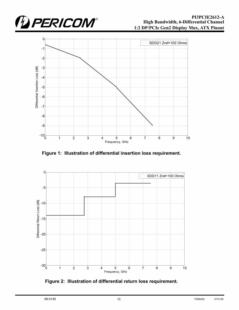
≥-[0.6*(f)+0.5] dB up to 2.5 GHz (for example, ≥-2 dB at f = 2.5 GHz);≥-[1.2*(f-2.5)+2] dB for 2.5 GHz < f ≤ 5 GHz (for exam-ple, ≥-5 dB at f = 5 GHz);≥-[1.6*(f-5)+5] dB for 5 GHz < f ≤ 7.5 GHz (for example, ≥-9 dB at f = 7.5 GHz);
dB
DDRL Differential Return Loss
≤ -14 dB up to 2.8 GHz; ≤ -8 dB up to 5 GHz; ≤ -4 dB up to 7.5 GHz.
dB
DDNEXT Near End Crosstalk -32 dB max up to 2.5 GHz; -26 dB max up to 5.0 GHz; -20 dB max up to 7.5 GHz;
dB
DDIL when switch is off
Differential Insertion Loss when switch is off
≤ -20 dB up to 3 GHz; dB
13 PS8925D 07/31/08
PI3PCIE2612-AHigh Bandwidth, 6-Differential Channel
1:2 DP/PCIe Gen2 Display Mux, ATX Pinout
08-0145
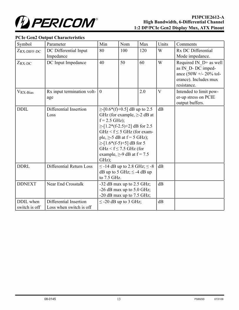
PCIe Gen2 Output CharacteristicsSymbol Parameter Min Nom Max Units CommentsZRX-DIFF-DC DC Differential Input
Impedance80 100 120 W Rx DC Differential
Mode impedance.ZRX-DC DC Input Impedance 40 50 60 W Required IN_D+ as well
as IN_D- DC imped-ance (50W +/- 20% tol-erance). Includes mux resistance.
VRX-Bias Rx input termination volt-age
0 2.0 V Intended to limit pow-er-up stress on PCIE output buffers.
DDIL Differential Insertion Loss
≥-[0.6*(f)+0.5] dB up to 2.5 GHz (for example, ≥-2 dB at f = 2.5 GHz);≥-[1.2*(f-2.5)+2] dB for 2.5 GHz < f ≤ 5 GHz (for exam-ple, ≥-5 dB at f = 5 GHz);≥-[1.6*(f-5)+5] dB for 5 GHz < f ≤ 7.5 GHz (for example, ≥-9 dB at f = 7.5 GHz);
dB
DDRL Differential Return Loss ≤ -14 dB up to 2.8 GHz; ≤ -8 dB up to 5 GHz; ≤ -4 dB up to 7.5 GHz.
dB
DDNEXT Near End Crosstalk -32 dB max up to 2.5 GHz; -26 dB max up to 5.0 GHz; -20 dB max up to 7.5 GHz;
dB
DDIL when switch is off
Differential Insertion Loss when switch is off
≤ -20 dB up to 3 GHz; dB

14 PS8925D 07/31/08
PI3PCIE2612-AHigh Bandwidth, 6-Differential Channel
1:2 DP/PCIe Gen2 Display Mux, ATX Pinout
08-0145
Display Port Output CharacteristicsSymbol Parameter Min Nom Max Units CommentsTbit Unit Interval 333 ps Normal Tbit at 2.7Gb/
s=370ps. 333ps=370ps-10%
VRX-Diffp-p Differential Input Peak to Peak Voltage
0.340 1.38 V VRX-DIFFp-p = 2*|VRX-D+ - VRX-D-|. Applies to IN_D and RX_IN signals.
TJIT Jitter added to high-speed signals
7.4 ps Jitter budget for high-speed signals as they pass through the display mux.7.4ps = 0.02 Tbit at 2.7Gb/s
DDIL Differential Insertion Loss
≥-[0.75*(f)+0.5] dB up to 1.35 GHz;≥-[2.2*(f-1.35)+1.5] dB for 1.35 GHz < f ≤ 2.7 GHz
dB For example, ≥-1.5 dB at f = 1.35 GHzFor example, ≥-4.5 dB at f = 2.7 GHz
DDRL Differential Return Loss ≤ -14 dB up to 2.7 GHz dBDDNEXT Near End Crosstalk -32 dB max up to 2.7 GHz dB
HPD Input CharacteristicsSymbol Parameter Min Nom Max Units CommentsVIH-HPD Input high level 3.6 V Low-speed input chang-
es state on cable plug/unplug.
VIL-HPD HPD Input Low Level 0 VIIN_HPD HPD input leakage cur-
rent|10| uA Measured with HPD
at VIH-HPD max and VIL-HPD min
THPD HPD_IN to HPD propa-gation delay.
200 ns Time from HPD_IN changing state to HPD changing state. Includes HPD rise/fall time.
TRF-HPD HPD rise/fall time. 1 20 ns Time required to transi-tion from VOH-HPD to VOL-HPD or fromVOL-HPD to VOH-HPD.
Termination ResistorsSymbol Parameter Min Nom Max Units CommentsRDDC DDC Termination Resis-
tors1.3K 1.5k 2.2k W Applies to both 3.3V
and 5V pull up resistors.

15 PS8925D 07/31/08
PI3PCIE2612-AHigh Bandwidth, 6-Differential Channel
1:2 DP/PCIe Gen2 Display Mux, ATX Pinout
08-0145
Signal Integrity Requirements and Test Procedures for 5.0 Gb/sParameter Procedure RequirementsDifferential Insertion Loss (DDIL)
EIA 364-101The EIA standard shall be used with the following considerations:1. The measured differential S parameter shall be referenced to a 100 ohms differential impedance.2. The test fixture shall meet the test fixture requirement defined in Section 1.12.3. The test fixture effect shall be removed from the measured S parameters. Refer to Note 1.
≥-[0.6*(f)+0.5] dB up to 2.5 GHz (for example, ≥-2 dB at f = 2.5 GHz);≥-[1.2*(f-2.5)+2] dB for 2.5 GHz < f ≤ 5 GHz (for example, ≥-5 dB at f = 5 GHz);≥-[1.6*(f-5)+5] dB for 5 GHz < f ≤ 7.5 GHz (for example, ≥-9 dB at f = 7.5 GHz);Refer to Figure 1.
Differential Return Loss (DDRL)
EIA 364-108The EIA standard shall be used with the following considerations:1. The measured differential S parameter shall be referenced to a 100 ohms differential impedance.2. The test fixture shall meet the test fixture requirement in Section 1.12.3. The test fixture effect shall be removed. Refer to Note 1.
≤ -14 dB up to 2.8 GHz; ≤ -8 dB up to 5 GHz; ≤ -4 dB up to 7.5 GHz.Refer to Figure 2.
Intra-pair Skew Intra-pair skew must be achieved by design; measurement not required.
5 ps max
Differential Near End Crosstalk (DDNEXT)
EIA 364-90The EIA standard must be used with the following considerations:1. The crosstalk requirement is with respect to all the adjacent dif-ferential pairs
-32 dB max up to 2.5 GHz;-26 dB max up to 5.0 GHz;-20 dB max up to 7.5 GHz;See Figure 3.
Differential Insertion Loss (DDIL) when switch is turned off
EIA 364-101 ≤ -20 dB up to 3 GHz;
Notes:1. The specified S parameters requirements are for switch component only, not including the test fixture effect. While the TRL calibration method is recommended, other calibration methods are allowed.
Switch Signal Integrity Requirements and Test Procedures for 5.0 Gb/s
Signal integrity requirements for 5.0 Gb/s applications of the switch are specified. Also included are the requirements of the test fixture for switch S-parameter measurements.
Signal Integrity Requirements
The procedures outlined in ANSI Electronics Industry Alliance (EIA) standards documents shall be followed:
• EIA 364-101 – Attenuation Test Procedure for Electrical Connectors, Sockets, Cable Assemblies or Interconnection Systems • EIA 364-90 – Crosstalk Ratio Test Procedure for Electrical Connectors, Sockets, Cable Assemblies or Interconnection Systems • EIA 364-108- Impedance, Reflection Coefficient, Return Loss, and VSWR Measured in the Time and Frequency Do-main Test Procedure for Electrical Connectors, Sockets, Cable Assemblies or Interconnection Systems
16 PS8925D 07/31/08
PI3PCIE2612-AHigh Bandwidth, 6-Differential Channel
1:2 DP/PCIe Gen2 Display Mux, ATX Pinout
08-0145
0 1 2 3 4 5 6 7 8 9 10-10
-9
-8
-7
-6
-5
-4
-3
-2
-1
0
Frequency, GHz
Diff
eren
tial I
nser
tion
Loss
[dB
]
SDD21 Zref=100 Ohms
Figure 1: Illustration of differential insertion loss requirement.
0 1 2 3 4 5 6 7 8 9 10-30
-25
-20
-15
-10
-5
0
Frequency, GHz
Diff
eren
tial R
etur
n Lo
ss [d
B]
SDD11 Zref=100 Ohms
Figure 2: Illustration of differential return loss requirement.
17 PS8925D 07/31/08
PI3PCIE2612-AHigh Bandwidth, 6-Differential Channel
1:2 DP/PCIe Gen2 Display Mux, ATX Pinout
08-0145
0 1 2 3 4
-10
5 6 7 8-45
-40
-35
-30
-25
-20
SDD21 Zref=85 Ohms
-15
Frequency, GHz
Diff
eren
tial N
ear E
nd C
ross
talk
, dB
Figure 3: Illustration of different ial near end crosstalk requirement.
Switch Test Fixture Requirements
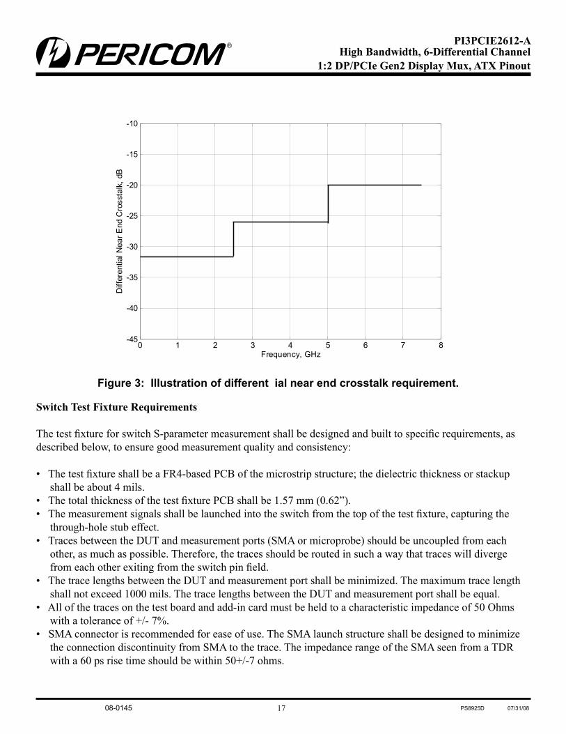
The test fixture for switch S-parameter measurement shall be designed and built to specific requirements, as described below, to ensure good measurement quality and consistency:
• The test fixture shall be a FR4-based PCB of the microstrip structure; the dielectric thickness or stackup shall be about 4 mils. • The total thickness of the test fixture PCB shall be 1.57 mm (0.62”). • The measurement signals shall be launched into the switch from the top of the test fixture, capturing the through-hole stub effect. • Traces between the DUT and measurement ports (SMA or microprobe) should be uncoupled from each other, as much as possible. Therefore, the traces should be routed in such a way that traces will diverge from each other exiting from the switch pin field. • The trace lengths between the DUT and measurement port shall be minimized. The maximum trace length shall not exceed 1000 mils. The trace lengths between the DUT and measurement port shall be equal. • All of the traces on the test board and add-in card must be held to a characteristic impedance of 50 Ohms with a tolerance of +/- 7%. • SMA connector is recommended for ease of use. The SMA launch structure shall be designed to minimize the connection discontinuity from SMA to the trace. The impedance range of the SMA seen from a TDR with a 60 ps rise time should be within 50+/-7 ohms.
18 PS8925D 07/31/08
PI3PCIE2612-AHigh Bandwidth, 6-Differential Channel
1:2 DP/PCIe Gen2 Display Mux, ATX Pinout
08-0145
Ordering InformationOrdering Code Package Code Package Description
PI3PCIE2612-AZFE ZF Pb-free & Green, 56-contact TQFN
Notes:• Thermal characteristics can be found on the company web site at www.pericom.com/packaging/ • "E" denotes Pb-free and Green• Adding an "X" at the end of the ordering code denotes tape and reel packaging
Packaging Mechanical: 56-Contact TQFN (ZFE)
1
DESCRIPTION: 56-contact, Thin Fine Pitch Quad Flat No-lead (TQFN)PACKAGE CODE: ZF56
DOCUMENT CONTROL #: PD-2024 REVISION: C
DATE: 05/15/08
08-0208
Pericom Semiconductor Corporation • 1-800-435-2336 • www.pericom.com

](https://static.fdocuments.in/doc/165x107/577c82771a28abe054b0e1ed/fisiology-homeostasis-sel-compatibility-mode1.jpg)