PHYSICAL REVIEW ACCELERATORS AND BEAMS 24, 082002 (2021)
11
Electrodeposition of copper applied to the manufacture of seamless superconducting rf cavities L. Lain Amador , * P. Chiggiato, L. M. A. Ferreira , E. Garcia-Tabares , T. Koettig, M. S. Meyer, A. T. Perez-Fontenla , K. Puthran , G. Rosaz , and M. Taborelli CERN, 1211 Geneva 23, Switzerland (Received 6 May 2021; accepted 26 July 2021; published 16 August 2021) Niobium thin film coated copper superconducting radio frequency elliptical cavities have demonstrated for many years their strong potential as an alternative to bulk niobium cavities. The thin film lower performance at high rf field is often attributed to the defects observed in the elaborated Nb layer, sometimes originated from defects inherited from the substrate itself. The currently used methods of manufacturing the copper elliptical substrates include several steps of electron-beam welding in order to join the half cells and the cutoffs which can contribute to defects and porosities. Seamless methods are nowadays developed in order to avoid welding steps and to decrease the global manufacturing cost of the cavities. We propose in this study an innovative alternative route in which the cavity is formed by electrodeposition of copper on a sacrificial aluminum mandrel. The strength of the process relies on the total absence of welding joints. Two different electroforming techniques using either direct current or pulsed plating have been investigated. The electroformed copper exhibited similar mechanical robustness, cryogenic properties and purity as the oxygen-free copper. In addition, the fabrication process was validated on test mandrels which mimic the geometry of 1.3 GHz cavities. DOI: 10.1103/PhysRevAccelBeams.24.082002 I. INTRODUCTION Radio frequency cavities are resonant devices used in particle accelerators to accelerate charged particle beams. Although cavities can be built of normal conducting materials, the use of superconducting ones increases the portion of the rf energy that accelerates the beam, reducing losses by heat dissipation on the cavity wall. Very good performance is obtained from massive niobium cavities which have a very low surface resistance [1]. However, the high cost of niobium triggered the research of less expensive and more efficient cavity fabrication methods as, for example, through the use of thin films [2,3]. At CERN, Nb coating on copper technology was developed and was successfully used for the production of cavities for the Large Electron Positron Collider (LEP) and was chosen again for the quarter wave resonators (QWR) fabrication of the HIE-ISOLDE beam facility [4]. The bottleneck of Nb thin films is the strong increase of surface resistance as a function of the rf field amplitude which makes the technology adapted only to low-accelerating gradient applications. Calatroni et al. [5,6] suggested that the film defects, which are sometimes observed in the deposited Nb layer, could explain the limits of the rf performance. Those are sometimes originated from defects inherited from the copper substrate itself. This was observed with the HIE- ISOLDE QWR coated cavities, where a systematic loss of performance observed on the electron-beam welded cavities revealed the importance of using seamless sub- strates [7]. Moreover, Palmieri et al. introduced a thermal boundary model which explained the decrease of rf performance based on the quality of the thermal contact at the Nb/Cu interface [8]. Superconducting radio frequency (SRF) copper elliptical cavity substrates are normally manufactured via sheet metal working and welding. The process consists in the forming of the two separated half cells by using either a spinning or electro-hydroforming process. Both are then joined together and to the cutoffs by electron-beam welding (see Fig. 1 for nomenclature). In this approach, porosities can potentially form along the junction line. On top of that, the welding seams are localized in crucial regions such as the iris and equator, which are very critical for rf performance because they are respectively exposed to high electric and magnetic field [9]. Manufacturing of seamless cavities has been approached by different methods over the past decades [10]. Hydroforming was first explored at Cornell University [11] and at CERN [12]. Here the cavity is produced by * [email protected] Published by the American Physical Society under the terms of the Creative Commons Attribution 4.0 International license. Further distribution of this work must maintain attribution to the author(s) and the published article’s title, journal citation, and DOI. PHYSICAL REVIEW ACCELERATORS AND BEAMS 24, 082002 (2021) 2469-9888=21=24(8)=082002(11) 082002-1 Published by the American Physical Society
Transcript of PHYSICAL REVIEW ACCELERATORS AND BEAMS 24, 082002 (2021)

Electrodeposition of copper applied to the manufactureof seamless superconducting rf cavities
L. Lain Amador ,* P. Chiggiato, L. M. A. Ferreira , E. Garcia-Tabares , T. Koettig,M. S. Meyer, A. T. Perez-Fontenla , K. Puthran , G. Rosaz , and M. Taborelli
CERN, 1211 Geneva 23, Switzerland
(Received 6 May 2021; accepted 26 July 2021; published 16 August 2021)
Niobium thin film coated copper superconducting radio frequency elliptical cavities have demonstratedfor many years their strong potential as an alternative to bulk niobium cavities. The thin film lowerperformance at high rf field is often attributed to the defects observed in the elaborated Nb layer, sometimesoriginated from defects inherited from the substrate itself. The currently used methods of manufacturing thecopper elliptical substrates include several steps of electron-beam welding in order to join the half cells andthe cutoffs which can contribute to defects and porosities. Seamless methods are nowadays developed inorder to avoid welding steps and to decrease the global manufacturing cost of the cavities. We propose inthis study an innovative alternative route in which the cavity is formed by electrodeposition of copper on asacrificial aluminum mandrel. The strength of the process relies on the total absence of welding joints.Two different electroforming techniques using either direct current or pulsed plating have beeninvestigated. The electroformed copper exhibited similar mechanical robustness, cryogenic propertiesand purity as the oxygen-free copper. In addition, the fabrication process was validated on test mandrelswhich mimic the geometry of 1.3 GHz cavities.
DOI: 10.1103/PhysRevAccelBeams.24.082002
I. INTRODUCTION
Radio frequency cavities are resonant devices used inparticle accelerators to accelerate charged particle beams.Although cavities can be built of normal conductingmaterials, the use of superconducting ones increases theportion of the rf energy that accelerates the beam, reducinglosses by heat dissipation on the cavity wall. Very goodperformance is obtained from massive niobium cavitieswhich have a very low surface resistance [1]. However,the high cost of niobium triggered the research of lessexpensive and more efficient cavity fabrication methods as,for example, through the use of thin films [2,3]. At CERN,Nb coating on copper technology was developed and wassuccessfully used for the production of cavities for theLarge Electron Positron Collider (LEP) and was chosenagain for the quarter wave resonators (QWR) fabricationof the HIE-ISOLDE beam facility [4]. The bottleneck ofNb thin films is the strong increase of surface resistanceas a function of the rf field amplitude which makes thetechnology adapted only to low-accelerating gradient
applications. Calatroni et al. [5,6] suggested that the filmdefects, which are sometimes observed in the deposited Nblayer, could explain the limits of the rf performance. Thoseare sometimes originated from defects inherited from thecopper substrate itself. This was observed with the HIE-ISOLDE QWR coated cavities, where a systematic loss ofperformance observed on the electron-beam weldedcavities revealed the importance of using seamless sub-strates [7]. Moreover, Palmieri et al. introduced a thermalboundary model which explained the decrease of rfperformance based on the quality of the thermal contactat the Nb/Cu interface [8].Superconducting radio frequency (SRF) copper elliptical
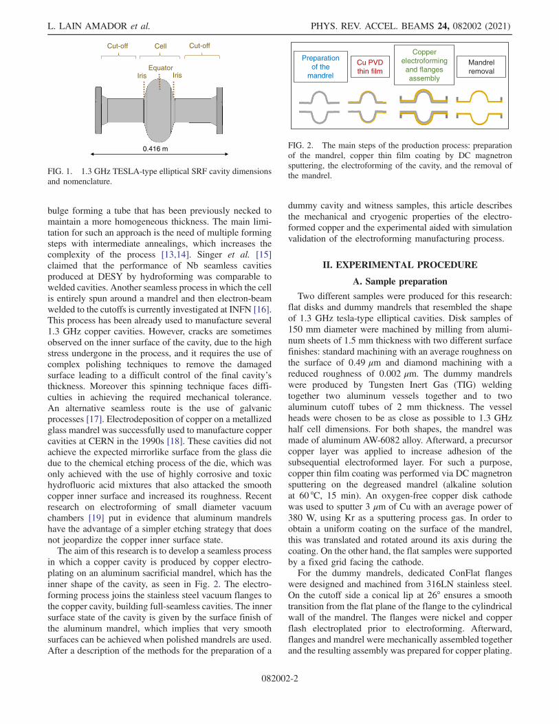
cavity substrates are normally manufactured via sheet metalworking and welding. The process consists in the formingof the two separated half cells by using either a spinningor electro-hydroforming process. Both are then joinedtogether and to the cutoffs by electron-beam welding(see Fig. 1 for nomenclature). In this approach, porositiescan potentially form along the junction line. On top of that,the welding seams are localized in crucial regions suchas the iris and equator, which are very critical for rfperformance because they are respectively exposed to highelectric and magnetic field [9].Manufacturing of seamless cavities has been approached
by different methods over the past decades [10].Hydroforming was first explored at Cornell University[11] and at CERN [12]. Here the cavity is produced by
Published by the American Physical Society under the terms ofthe Creative Commons Attribution 4.0 International license.Further distribution of this work must maintain attribution tothe author(s) and the published article’s title, journal citation,and DOI.
PHYSICAL REVIEW ACCELERATORS AND BEAMS 24, 082002 (2021)
2469-9888=21=24(8)=082002(11) 082002-1 Published by the American Physical Society
bulge forming a tube that has been previously necked tomaintain a more homogeneous thickness. The main limi-tation for such an approach is the need of multiple formingsteps with intermediate annealings, which increases thecomplexity of the process [13,14]. Singer et al. [15]claimed that the performance of Nb seamless cavitiesproduced at DESY by hydroforming was comparable towelded cavities. Another seamless process in which the cellis entirely spun around a mandrel and then electron-beamwelded to the cutoffs is currently investigated at INFN [16].This process has been already used to manufacture several1.3 GHz copper cavities. However, cracks are sometimesobserved on the inner surface of the cavity, due to the highstress undergone in the process, and it requires the use ofcomplex polishing techniques to remove the damagedsurface leading to a difficult control of the final cavity’sthickness. Moreover this spinning technique faces diffi-culties in achieving the required mechanical tolerance.An alternative seamless route is the use of galvanicprocesses [17]. Electrodeposition of copper on a metallizedglass mandrel was successfully used to manufacture coppercavities at CERN in the 1990s [18]. These cavities did notachieve the expected mirrorlike surface from the glass diedue to the chemical etching process of the die, which wasonly achieved with the use of highly corrosive and toxichydrofluoric acid mixtures that also attacked the smoothcopper inner surface and increased its roughness. Recentresearch on electroforming of small diameter vacuumchambers [19] put in evidence that aluminum mandrelshave the advantage of a simpler etching strategy that doesnot jeopardize the copper inner surface state.The aim of this research is to develop a seamless process
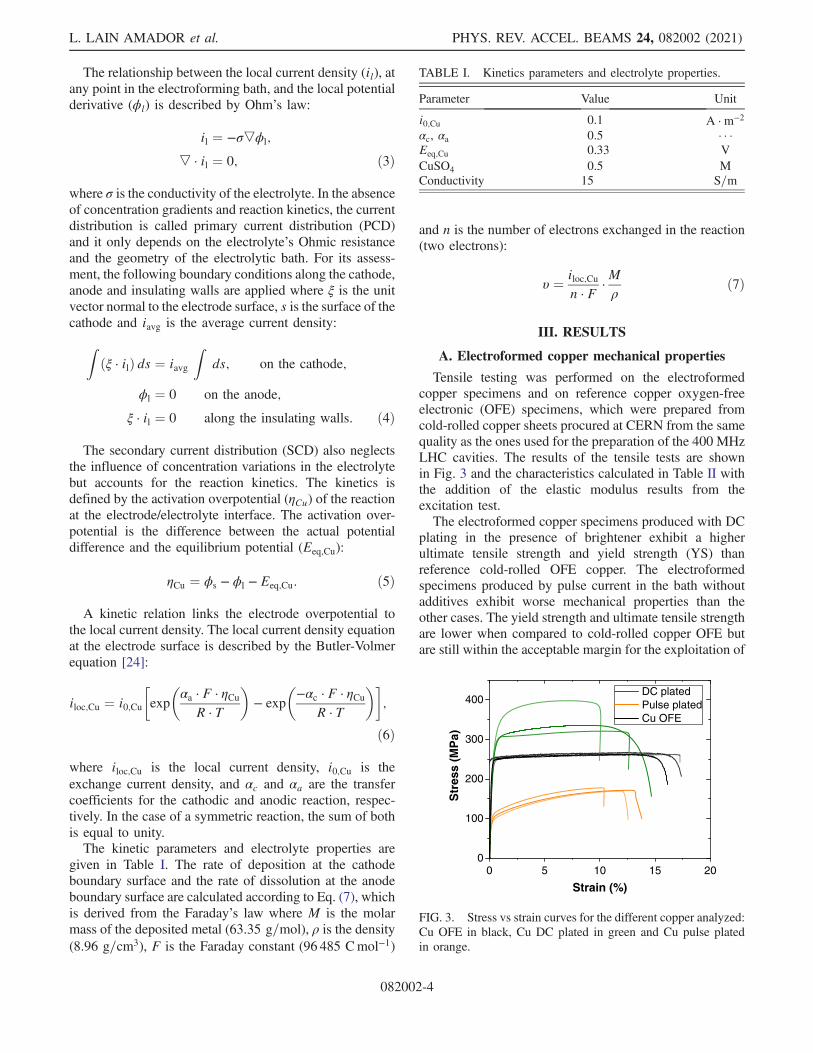
in which a copper cavity is produced by copper electro-plating on an aluminum sacrificial mandrel, which has theinner shape of the cavity, as seen in Fig. 2. The electro-forming process joins the stainless steel vacuum flanges tothe copper cavity, building full-seamless cavities. The innersurface state of the cavity is given by the surface finish ofthe aluminum mandrel, which implies that very smoothsurfaces can be achieved when polished mandrels are used.After a description of the methods for the preparation of a
dummy cavity and witness samples, this article describesthe mechanical and cryogenic properties of the electro-formed copper and the experimental aided with simulationvalidation of the electroforming manufacturing process.
II. EXPERIMENTAL PROCEDURE
A. Sample preparation
Two different samples were produced for this research:flat disks and dummy mandrels that resembled the shapeof 1.3 GHz tesla-type elliptical cavities. Disk samples of150 mm diameter were machined by milling from alumi-num sheets of 1.5 mm thickness with two different surfacefinishes: standard machining with an average roughness onthe surface of 0.49 μm and diamond machining with areduced roughness of 0.002 μm. The dummy mandrelswere produced by Tungsten Inert Gas (TIG) weldingtogether two aluminum vessels together and to twoaluminum cutoff tubes of 2 mm thickness. The vesselheads were chosen to be as close as possible to 1.3 GHzhalf cell dimensions. For both shapes, the mandrel wasmade of aluminum AW-6082 alloy. Afterward, a precursorcopper layer was applied to increase adhesion of thesubsequential electroformed layer. For such a purpose,copper thin film coating was performed via DC magnetronsputtering on the degreased mandrel (alkaline solutionat 60 °C, 15 min). An oxygen-free copper disk cathodewas used to sputter 3 μm of Cu with an average power of380 W, using Kr as a sputtering process gas. In order toobtain a uniform coating on the surface of the mandrel,this was translated and rotated around its axis during thecoating. On the other hand, the flat samples were supportedby a fixed grid facing the cathode.For the dummy mandrels, dedicated ConFlat flanges
were designed and machined from 316LN stainless steel.On the cutoff side a conical lip at 26° ensures a smoothtransition from the flat plane of the flange to the cylindricalwall of the mandrel. The flanges were nickel and copperflash electroplated prior to electroforming. Afterward,flanges and mandrel were mechanically assembled togetherand the resulting assembly was prepared for copper plating.
Preparation of the
mandrel
Copper electroforming
and flanges assembly
Mandrel removal
Cu PVD thin film
FIG. 2. The main steps of the production process: preparationof the mandrel, copper thin film coating by DC magnetronsputtering, the electroforming of the cavity, and the removal ofthe mandrel.
CellCut-off Cut-off
Iris IrisEquator
0.416 m
FIG. 1. 1.3 GHz TESLA-type elliptical SRF cavity dimensionsand nomenclature.
L. LAIN AMADOR et al. PHYS. REV. ACCEL. BEAMS 24, 082002 (2021)
082002-2

The flat disk samples were held on a specific support,which protected the rear side of the aluminum plate.The samples were copper plated in an acidic copper
sulfate bath (Cu 38 g=l, H2SO4 100 ml=l) using twodifferent plating procedures: pulse plating on the mentionedbath without additives or direct current plating adding acommercial complex brightener to increase smoothness.The applied average current density for both processes was160 A · m−2. The pulse plating was performed in pulses of7 ms on-time and 8 ms off-time.Finally, the electroformed disk/assembly underwent
chemical etching on NaOH 200 g=l to remove the alumi-num mandrel. After complete removal of the mandrel,acidic ammonium persulfate rinsing (150 g=l) was per-formed to remove surface impurities, which were part ofthe aluminum alloy and are not removed by the NaOHsolution [20]. At the end of the process, the samples wererinsed with deionized water followed with ethanol andfinally dried. After this step, the copper coating was visibleon the inner surface of the disk or test cavity.
B. Sample characterization methods
Standard tensile specimens and rectangular samples“L” (20 mm × 60 mm), “M” (10 mm × 20 mm) and “S”(2 mm × 110 mm) were extracted from the 2 mm thickelectroformed disks by electroerosion cutting. Mechanicaltests were performed on the specimens with an ultimatetensile strength (UTS) electromechanical testing machineequipped with a 200 kN load cell. The Young’s moduluswas calculated by the impulse excitation technique on therectangular samples “L” following ASTM-E1876 [21]. Themicrostructure of the electroformed copper was observedon a LEICA Q600 optical microscope after the samplesof dimension “M” were polished and chemically etched(5 g of FeCl3, 50 ml of HCl and 100 ml of H2O). Thesurface roughness was measured on the surface of samples“M” with a surface optical profiler VEECO-NT 3300.The residual resistivity ratio (RRR) and thermal con-
ductivity were measured on “S” samples, which wereetched with ammonium persulfate (50 μm removal) andpassivated in chromic acid to remove the oxide layerproduced during the cutting [22].RRR was determined by measuring the samples in a
four-wire configuration with an electrical current of 5 A.The respective voltage drop was determined at the samplelength of 110 mm. The samples themselves were thermal-ized on a Cu platform surrounded by a thermal shield all ininsulation vacuum of p < 10−6 mbar. The samples wereconduction cooled via Kapton tape electrical insulatorswith the cooling provided by a helium phase separator,which was kept at 4.2 K helium saturation conditions. Thecryostat setup allowed the measurement of the electricalresistance of the samples at room temperature and at 4.2 Kwithout altering the four-wire electrical contacts on thesamples. Given the fact that the thermal screen minimized
heat loads to the sample environment and all incomingcabling was thermally anchored at the thermal screen andthe phase separator stages, the estimated measurement errorfor the sample temperature was dT4.2 K ¼ �0.08 K and thedT293 K � 0.6 K. The relative accuracy of the RRR valuewas then estimated to be ΔRRR=RRR ¼ �5%.Thermal conductivity measurements were performed
using a steady-state method [23] in the temperature rangebetween 3.5 and 40 K. An electric heater, mounted on thefree end of the sample, generated a heating power, _Q that inturn caused a temperature gradient ΔT along the activelength L of the sample; this ΔT was measured as therecorded temperature difference between two temperaturesensors mounted on the sample separated by characteristicor active length L. The thermal conductivity λ was obtainedfrom Fourier’s law of heat conduction between the appliedheat flux and recorded temperature difference [Eq. (1)]:
λ ¼_QL
AΔT; ð1Þ
where A is the cross-section area of the sample. Theexperimental platform was thermally linked to the secondstage of a pulse tube cryocooler via a copper rod. It reached2.9 K at no load and could provide up to 1W cooling powerat 4.2 K. Insulation vacuum in the order of 10−5 mbar wasreached before the system is cooled down. The measure-ment error calculation considered the precision of thecurrent sources, temperature measurements and uncertain-ties in sample dimensions. The absolute error for temper-ature measurement in the low temperature range (4.5 K)was ΔT ¼ �8 mK, whereas in the high temperature range(40 K) was ΔT ¼ �75 mK. The relative error for thethermal conductivity data was �1%.Copper impurity content of “L” samples was measured by
glow discharge mass spectrometry (GDMS) and interstitialgas analysis (IGA) in EAG laboratories (Tournefeuille,France). For the electroformed dummy cavities, the thick-ness of the electroplated layer was measured with anOlympus Magma-Mike 8600 thickness gauge.
C. Simulation methods
The electroforming process was modeled withCOMSOL Multiphysics using the electrodeposition pri-mary and secondary current distribution physics module.The boundary displacements resulting from the platedthickness at the cathode and the anodic dissolutionwere included in the simulation thanks to a movingmesh. The electron transfer reactions that take place onthe anode and the cathode are the following, assuming a100% yield:
Anode∶ CuðsÞ → Cu2þ þ 2e−
Cathode∶ Cu2þ þ 2e− → CuðsÞ: ð2Þ
ELECTRODEPOSITION OF COPPER APPLIED … PHYS. REV. ACCEL. BEAMS 24, 082002 (2021)
082002-3
The relationship between the local current density (il), atany point in the electroforming bath, and the local potentialderivative (ϕl) is described by Ohm’s law:
il ¼ −σ▽ϕl;
▽ · il ¼ 0; ð3Þ
where σ is the conductivity of the electrolyte. In the absenceof concentration gradients and reaction kinetics, the currentdistribution is called primary current distribution (PCD)and it only depends on the electrolyte’s Ohmic resistanceand the geometry of the electrolytic bath. For its assess-ment, the following boundary conditions along the cathode,anode and insulating walls are applied where ξ is the unitvector normal to the electrode surface, s is the surface of thecathode and iavg is the average current density:
Zðξ · ilÞ ds ¼ iavg
Zds; on the cathode;
ϕl ¼ 0 on the anode;
ξ · il ¼ 0 along the insulating walls: ð4Þ
The secondary current distribution (SCD) also neglectsthe influence of concentration variations in the electrolytebut accounts for the reaction kinetics. The kinetics isdefined by the activation overpotential (ηCu) of the reactionat the electrode/electrolyte interface. The activation over-potential is the difference between the actual potentialdifference and the equilibrium potential (Eeq;Cu):
ηCu ¼ ϕs − ϕl − Eeq;Cu: ð5Þ
A kinetic relation links the electrode overpotential tothe local current density. The local current density equationat the electrode surface is described by the Butler-Volmerequation [24]:
iloc;Cu ¼ i0;Cu
�exp
�αa · F · ηCu
R · T
�− exp
�−αc · F · ηCu
R · T
��;
ð6Þ
where iloc;Cu is the local current density, i0;Cu is theexchange current density, and αc and αa are the transfercoefficients for the cathodic and anodic reaction, respec-tively. In the case of a symmetric reaction, the sum of bothis equal to unity.The kinetic parameters and electrolyte properties are
given in Table I. The rate of deposition at the cathodeboundary surface and the rate of dissolution at the anodeboundary surface are calculated according to Eq. (7), whichis derived from the Faraday’s law where M is the molarmass of the deposited metal (63.35 g=mol), ρ is the density(8.96 g=cm3), F is the Faraday constant (96 485 Cmol−1)
and n is the number of electrons exchanged in the reaction(two electrons):
υ ¼ iloc;Cun · F
·Mρ
ð7Þ
III. RESULTS
A. Electroformed copper mechanical properties
Tensile testing was performed on the electroformedcopper specimens and on reference copper oxygen-freeelectronic (OFE) specimens, which were prepared fromcold-rolled copper sheets procured at CERN from the samequality as the ones used for the preparation of the 400 MHzLHC cavities. The results of the tensile tests are shownin Fig. 3 and the characteristics calculated in Table II withthe addition of the elastic modulus results from theexcitation test.The electroformed copper specimens produced with DC
plating in the presence of brightener exhibit a higherultimate tensile strength and yield strength (YS) thanreference cold-rolled OFE copper. The electroformedspecimens produced by pulse current in the bath withoutadditives exhibit worse mechanical properties than theother cases. The yield strength and ultimate tensile strengthare lower when compared to cold-rolled copper OFE butare still within the acceptable margin for the exploitation of
TABLE I. Kinetics parameters and electrolyte properties.
Parameter Value Unit
i0;Cu 0.1 A · m−2
αc, αa 0.5 � � �Eeq;Cu 0.33 VCuSO4 0.5 MConductivity 15 S=m
0 5 10 15 200
100
200
300
400
Str
ess
(MP
a)
Strain (%)
DC platedPulse platedCu OFE
FIG. 3. Stress vs strain curves for the different copper analyzed:Cu OFE in black, Cu DC plated in green and Cu pulse platedin orange.
L. LAIN AMADOR et al. PHYS. REV. ACCEL. BEAMS 24, 082002 (2021)
082002-4
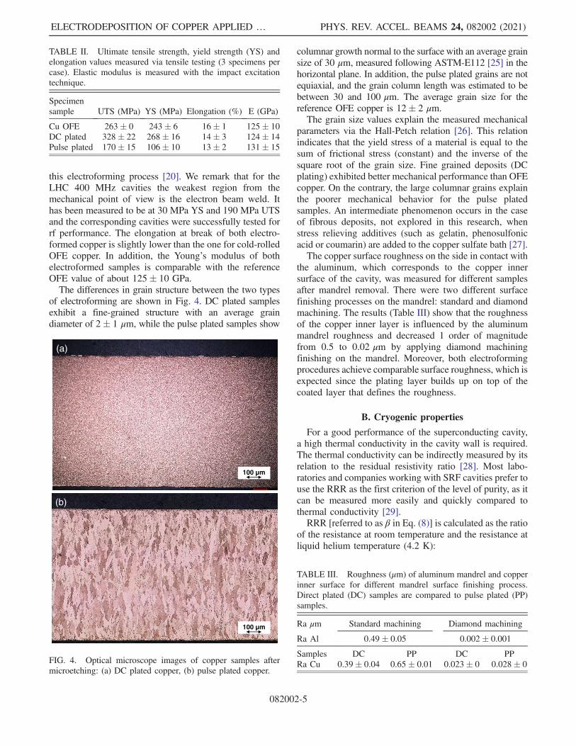
this electroforming process [20]. We remark that for theLHC 400 MHz cavities the weakest region from themechanical point of view is the electron beam weld. Ithas been measured to be at 30 MPa YS and 190 MPa UTSand the corresponding cavities were successfully tested forrf performance. The elongation at break of both electro-formed copper is slightly lower than the one for cold-rolledOFE copper. In addition, the Young’s modulus of bothelectroformed samples is comparable with the referenceOFE value of about 125� 10 GPa.The differences in grain structure between the two types
of electroforming are shown in Fig. 4. DC plated samplesexhibit a fine-grained structure with an average graindiameter of 2� 1 μm, while the pulse plated samples show
columnar growth normal to the surface with an average grainsize of 30 μm, measured following ASTM-E112 [25] in thehorizontal plane. In addition, the pulse plated grains are notequiaxial, and the grain column length was estimated to bebetween 30 and 100 μm. The average grain size for thereference OFE copper is 12� 2 μm.The grain size values explain the measured mechanical
parameters via the Hall-Petch relation [26]. This relationindicates that the yield stress of a material is equal to thesum of frictional stress (constant) and the inverse of thesquare root of the grain size. Fine grained deposits (DCplating) exhibited better mechanical performance than OFEcopper. On the contrary, the large columnar grains explainthe poorer mechanical behavior for the pulse platedsamples. An intermediate phenomenon occurs in the caseof fibrous deposits, not explored in this research, whenstress relieving additives (such as gelatin, phenosulfonicacid or coumarin) are added to the copper sulfate bath [27].The copper surface roughness on the side in contact with
the aluminum, which corresponds to the copper innersurface of the cavity, was measured for different samplesafter mandrel removal. There were two different surfacefinishing processes on the mandrel: standard and diamondmachining. The results (Table III) show that the roughnessof the copper inner layer is influenced by the aluminummandrel roughness and decreased 1 order of magnitudefrom 0.5 to 0.02 μm by applying diamond machiningfinishing on the mandrel. Moreover, both electroformingprocedures achieve comparable surface roughness, which isexpected since the plating layer builds up on top of thecoated layer that defines the roughness.
B. Cryogenic properties
For a good performance of the superconducting cavity,a high thermal conductivity in the cavity wall is required.The thermal conductivity can be indirectly measured by itsrelation to the residual resistivity ratio [28]. Most labo-ratories and companies working with SRF cavities prefer touse the RRR as the first criterion of the level of purity, as itcan be measured more easily and quickly compared tothermal conductivity [29].RRR [referred to as β in Eq. (8)] is calculated as the ratio
of the resistance at room temperature and the resistance atliquid helium temperature (4.2 K):
TABLE II. Ultimate tensile strength, yield strength (YS) andelongation values measured via tensile testing (3 specimens percase). Elastic modulus is measured with the impact excitationtechnique.
Specimensample UTS (MPa) YS (MPa) Elongation (%) E (GPa)
Cu OFE 263� 0 243� 6 16� 1 125� 10DC plated 328� 22 268� 16 14� 3 124� 14Pulse plated 170� 15 106� 10 13� 2 131� 15
100 µm
100 µm
(a)
(b)
FIG. 4. Optical microscope images of copper samples aftermicroetching: (a) DC plated copper, (b) pulse plated copper.
TABLE III. Roughness (μm) of aluminum mandrel and copperinner surface for different mandrel surface finishing process.Direct plated (DC) samples are compared to pulse plated (PP)samples.
Ra μm Standard machining Diamond machining
Ra Al 0.49� 0.05 0.002� 0.001
Samples DC PP DC PPRa Cu 0.39� 0.04 0.65� 0.01 0.023� 0 0.028� 0
ELECTRODEPOSITION OF COPPER APPLIED … PHYS. REV. ACCEL. BEAMS 24, 082002 (2021)
082002-5

β ¼ R298
R4.2: ð8Þ
The RRR results for the electroformed copper are shownin Fig. 5 and are compared to the copper OFE specification(RRR ¼ 50) [30]. The DC electroformed copper for as-deposited layers exhibits a lower RRR than the copper OFEspecification. Several heating steps improved the ratio up to115 after 400 °C treatment for 2 hours. In the case of pulseplated copper, the RRR value exceeds the specificationwith an average around 700 for as-deposited layers, whichis improved to 1600 after thermal annealing at 400 °C for2 hours. For both electroformed copper, the RRR increasedafter annealing which favors the removal of interstitialimpurities in the material. In the work of Kim et al. [31] andFickett [32], the RRR of OFE copper also increases withheat treatment upon a maximum of 300 at 500 °C.Due to the very high RRR values reported. which are
close to the sensitivity limit of our four-probes system,we decided to perform thermal conductivity measurementsin order to cross-check the values. In Fig. 6, the thermalconductivity value for the two electroformed coppermethods is assessed and compared with theoretical values
of conductivity for different RRR values [33]. The sampleswere measured just after deposition without thermaltreatment. The values are in agreement with the previousmeasured RRR, with higher values (RRR of 300–800) forpulse plated copper and lower values (RRR of 40) for theDC electroformed copper. The value expected for OFEcopper at 4.2 K is 400 Wm−1 K−1 (RRR ¼ 50), which isslightly higher than the value measured for the DC platedcopper. Pulse plated copper improves the thermal conduc-tivity by a factor of 5.The differences in thermal conductivity and RRR can be
explained by the level of impurities and lattice defects in thematerial [29,34]. The copper purity was qualified by meansof IGA and GDMS and compared with reference valuesof copper OFE [30]. The results are shown in Table IV.The differences on impurity-level between the DC plated
(a)
(b)
FIG. 5. Residual resistivity ratio (RRR) values for (a) DC platedcopper and (b) pulse plated copper at room temperature and afterseveral annealing steps. Cu OFE specification is added as areference from [30].
10 100100
1000
10000
RRR 30
RRR 100
RRR 300
I(W
/(m
K))
T (K)
DC plated (1)DC plated (2)Pulse plated (1)Pulse plated (2)
RRR 1000
FIG. 6. Dependence of Cu thermal conductivity on temperaturefor different RRR extracted from Ref. [33]. Experimental valuesfor the DC plated (green) and pulse plated samples (orange) areadded to the plot.
TABLE IV. Chemical composition of electroformed coppercompared to OFE copper (* indicates maximum values acceptedextracted from the standard OFE specification [30]).
Impurity(ppm wt.) Cu OFE* DC plated
Pulseplated
Labtechnique
Ag 25 3.2 0.1 GDMSAs 5 0 0 GDMSCl � � � 10 2.3 GDMSFe 10 0 0 GDMSPb 5 0 0 GDMSS 15 16 0.2 GDMSNi 10 0 0 GDMSTe 2 0 0 GDMSC 1 11 2 IGAO 5 6.2 2.8 IGAH � � � 0.4 0.1 IGA
L. LAIN AMADOR et al. PHYS. REV. ACCEL. BEAMS 24, 082002 (2021)
082002-6
and pulse plated copper are evidenced. Pulse plated coppercontains very low amount of impurities. Liu et al. [35]reported that the use of a complex brightener duringdeposition is known to incorporate impurities into thedeposit. This is in agreement with the presence of higherquantities of Cl, S, C, H and O on the DC plated copper.The oxygen content on this copper is higher than theOFE-Cu specification limit of 5 ppm and explains thepoorer RRR value. Previous studies [20] found that H2,oxygen and CO2 are released from the DC plated copperduring heating in vacuum. This agrees with the RRRincrease with annealing temperature shown in Fig. 5.However, the increment remains below what is reportedby Kim et al. [31] on OFE copper (RRR of 250 after 400 °Cheat treatment) because other impurities like Cl and S arestill strongly bonded to the copper lattice [36]. The DCplated samples were subjected again to GDMS analysisafter 400 °C annealing treatment and the quantities of Cland S remained similar (9 and 14 ppm wt. respectively) tothose measured after deposition (Table IV). The pulseplated copper exhibits purer composition than the OFEcopper, with a lower content of Ag, S and O. This couldexplain the high RRR values obtained and is an indicationof the good quality of this copper for rf application.The DC plated substrate might eventually be annealed to
400 °C to increase the RRR. The mechanical properties ofthe annealed electroformed copper were not assessed yetwith standard tensile testing, but were studied by meansof Vickers microhardness HV 0.1 (Table V). The micro-hardness of the DC plated copper decreased from 117� 3to 80� 1 (HV 0.1, 10 s) after 400 °C (2 hours) heattreatment, showing a similar trend as OFE copper, where adecrease from 83� 2 to 52� 1 (HV 0.1, 10 s) is observed.The hardness values for the DC plated copper after 400 °Cannealing are similar to those for OFE at room temperature.Therefore for the DC plated copper, the mechanicalproperties are expected to decrease and still remain strong.In addition the pulse plated copper, already exhibitingcoarse grains after deposition, only suffers a slight decreasein hardness after annealing. The results after 400 °Cannealing are very similar to those measured on theannealed OFE copper. In addition, the average grain areawas analyzed by electron backscatter diffraction (EBSD)after polishing the copper samples. The grain area ispreferred to the grain diameter due to the nonequiaxialgrains which are present on the pulse plated copper. Theresults, Table VI, show grain growth as a consequence of
recrystallization for the DC plated copper (5 times moregrain area) after 400 °C, 2 hours heat treatment. For thepulse plated copper, the grain growth is minimal. Thistrend is in agreement with the measured change in micro-hardness (Table V).
C. Cavity electroforming assessment
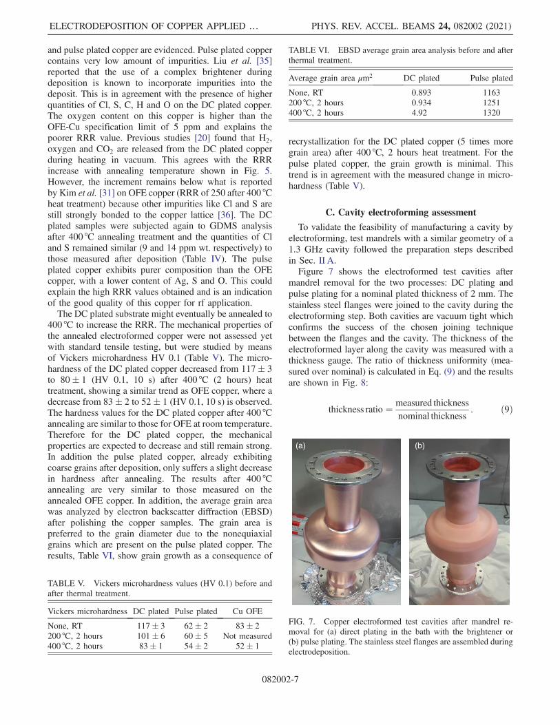
To validate the feasibility of manufacturing a cavity byelectroforming, test mandrels with a similar geometry of a1.3 GHz cavity followed the preparation steps describedin Sec. II A.Figure 7 shows the electroformed test cavities after
mandrel removal for the two processes: DC plating andpulse plating for a nominal plated thickness of 2 mm. Thestainless steel flanges were joined to the cavity during theelectroforming step. Both cavities are vacuum tight whichconfirms the success of the chosen joining techniquebetween the flanges and the cavity. The thickness of theelectroformed layer along the cavity was measured with athickness gauge. The ratio of thickness uniformity (mea-sured over nominal) is calculated in Eq. (9) and the resultsare shown in Fig. 8:
thickness ratio ¼ measured thicknessnominal thickness
: ð9Þ
TABLE V. Vickers microhardness values (HV 0.1) before andafter thermal treatment.
Vickers microhardness DC plated Pulse plated Cu OFE
None, RT 117� 3 62� 2 83� 2200 °C, 2 hours 101� 6 60� 5 Not measured400 °C, 2 hours 83� 1 54� 2 52� 1
TABLE VI. EBSD average grain area analysis before and afterthermal treatment.
Average grain area μm2 DC plated Pulse plated
None, RT 0.893 1163200 °C, 2 hours 0.934 1251400 °C, 2 hours 4.92 1320
(a) (b)
FIG. 7. Copper electroformed test cavities after mandrel re-moval for (a) direct plating in the bath with the brightener or(b) pulse plating. The stainless steel flanges are assembled duringelectrodeposition.
ELECTRODEPOSITION OF COPPER APPLIED … PHYS. REV. ACCEL. BEAMS 24, 082002 (2021)
082002-7
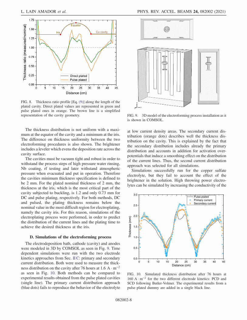
The thickness distribution is not uniform with a maxi-mum at the equator of the cavity and a minimum at the iris.The difference on thickness uniformity between the twoelectroforming procedures is also shown. The brightenerincludes a leveler which evens the deposition rate across thecavity surface.The cavities must be vacuum tight and robust in order to
withstand the process steps of high pressure water rinsing,Nb coating, rf testing and later withstand atmosphericpressure when evacuated and put in operation. Thereforethe cavities minimum thickness specification is defined tobe 2 mm. For the plated nominal thickness of 2 mm, thethickness at the iris, which is the most critical part of thecavity subjected to buckling, is 1.2 and only 0.73 mm forDC and pulse plating, respectively. For both methods, DCand pulsed, the plating thickness remains below thenominal value in the most difficult region for electroplating,namely the cavity iris. For this reason, simulations of theelectroplating process were performed, in order to predictthe distribution of the current lines and the plating time toachieve the desired thickness at the iris.
D. Simulations of the electroforming process
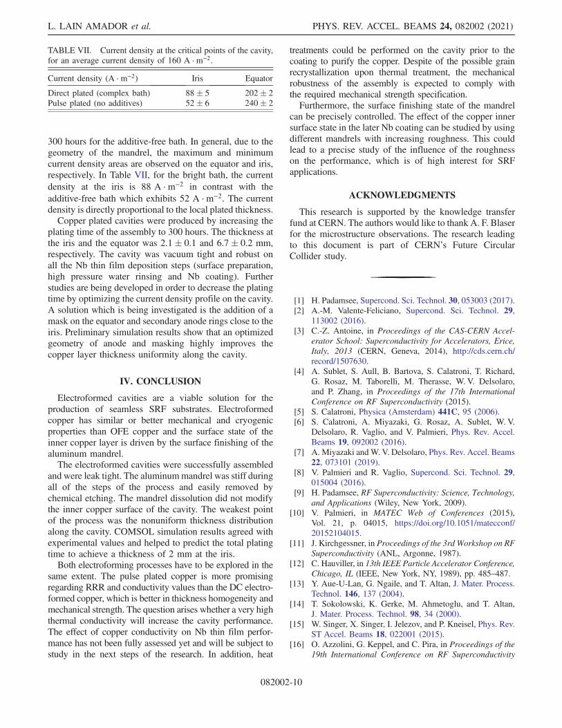
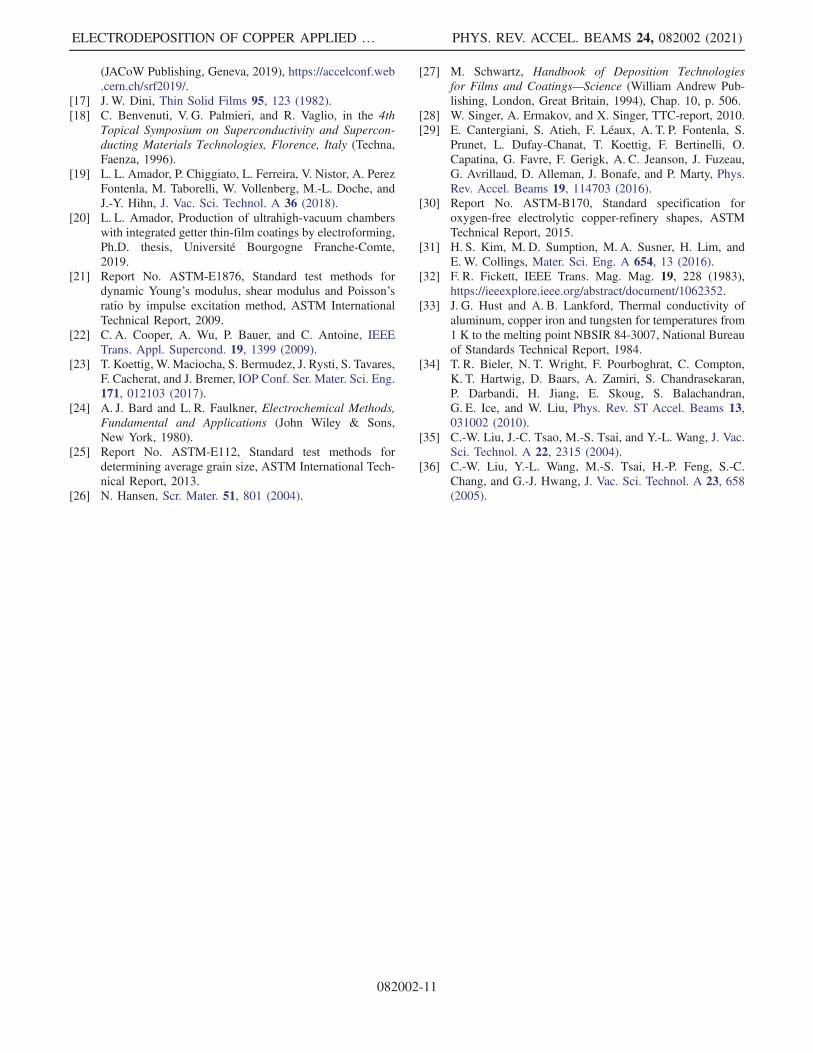
The electrodeposition bath, cathode (cavity) and anodeswere modeled in 3D by COMSOL as seen in Fig. 9. Timedependent simulations were run with the two electrodekinetics approaches from Sec. II C: primary and secondarycurrent distribution. Both were used to measure the thick-ness distribution on the cavity after 76 hours at 1.6 A · m−2
as seen in Fig. 10. Both methods can be compared toexperimental results obtained from the pulse plated cavities(single line). The primary current distribution approach(blue dots) fails to reproduce the behavior of the electrolyte
at low current density areas. The secondary current dis-tribution (orange dots) describes well the thickness dis-tribution on the cavity. This is explained by the fact thatthe secondary distribution includes already the primarydistribution and accounts in addition for activation over-potentials that induce a smoothing effect on the distributionof the current lines. Thus, the second current distributionapproach was selected for all simulations.Simulations successfully run for the copper sulfate
electrolyte, but they fail to account the effect of thebrightener in the solution. High throwing power electro-lytes can be simulated by increasing the conductivity of the
Cu cavity
Equator
Iris
FIG. 8. Thickness ratio profile [Eq. (9)] along the length of theplated cavity. Direct plated values are represented in green andpulse plated ones in orange. The brown line is a simplifiedrepresentation of the cavity geometry. FIG. 9. 3D model of the electroforming process installation as it
is shown in COMSOL.
0 5 10 15 20 25 30 35 40 450.0
0.5
1.0
1.5
2.0
2.5
3.0
Thi
ckne
ss(m
m)
Distance (cm)
Pulse platedPrimary currentSecondary current
FIG. 10. Simulated thickness distribution after 76 hours at160 A · m−2 for the two different electrode kinetics: PCD andSCD following Butler-Volmer. The experimental results from apulse plated dummy are added in a single black line.
L. LAIN AMADOR et al. PHYS. REV. ACCEL. BEAMS 24, 082002 (2021)
082002-8

bath. This effect can be observed in Fig. 11(a). Althoughin reality the brightener does not alter the electrolyteconductivity, which remains around 15 S=m, the increasein throwing power is assumed to act similarly. Thus, theartificial increase in conductivity which mimics theobserved increase in throwing power of the brighteneris investigated and compared with experimental values.Several simulations confirmed that a conductivity of80 S=m increases the throwing power, in similar fashionas the additive. In Fig. 11(b), the experimental values fromthe dummy cavities (Fig. 8) are then compared with thesimulated ones (for each electrolyte) with an averagedifference of around 8%.
After the successful validation of the model, simulationswere used to calculate the electroplating time to obtain aminimum thickness of 2 mm in the iris of the cavity, foreach bath. In this case, the model was simplified to a 2Dgeometry, which is valid for cylindrical symmetry geom-etries. The current density and thickness profile of thecavity were obtained as seen in Fig. 12. On the figure, thegeometry of the plated cavity represents the final shape ofthe object. On (a), the bath conductivity is set to 80 (S/m) tosimulate the bath with the brightener and on (b) to 15 (S/m)to simulate the bath without additives. The minimum time,which provides a thickness of 2 mm on the iris of the cavity,is 180 hours for the bright bath whereas it increases to
(a) (b)
FIG. 11. (a) COMSOL simulated thickness distribution along the cavity for different electrolyte conductivity values after 65 hoursplating at 160 A · m−2. (b) Comparison between the experimental thickness profile and the simulated one for the different electrolyteconductivities and different plating time.
Time=300 hoursTime=180 hours
mm
4
3
2
1
0
A/m2
250
200
150
100
50
0
mm
4
3
2
1
0
A/m2
250
200
150
100
50
0
80S/m
(a) (b)
15S/m
FIG. 12. COMSOL simulated deposited thickness (mm) along the cavity and electrolyte current lines distribution (A · m−2).(a) Solution from the bath with the brightener after 180 hours. (b) Solution from the bath without additives after 300 hours. In both casesthe average current density is 160 A · m−2.
ELECTRODEPOSITION OF COPPER APPLIED … PHYS. REV. ACCEL. BEAMS 24, 082002 (2021)
082002-9
300 hours for the additive-free bath. In general, due to thegeometry of the mandrel, the maximum and minimumcurrent density areas are observed on the equator and iris,respectively. In Table VII, for the bright bath, the currentdensity at the iris is 88 A · m−2 in contrast with theadditive-free bath which exhibits 52 A · m−2. The currentdensity is directly proportional to the local plated thickness.Copper plated cavities were produced by increasing the
plating time of the assembly to 300 hours. The thickness atthe iris and the equator was 2.1� 0.1 and 6.7� 0.2 mm,respectively. The cavity was vacuum tight and robust onall the Nb thin film deposition steps (surface preparation,high pressure water rinsing and Nb coating). Furtherstudies are being developed in order to decrease the platingtime by optimizing the current density profile on the cavity.A solution which is being investigated is the addition of amask on the equator and secondary anode rings close to theiris. Preliminary simulation results show that an optimizedgeometry of anode and masking highly improves thecopper layer thickness uniformity along the cavity.
IV. CONCLUSION
Electroformed cavities are a viable solution for theproduction of seamless SRF substrates. Electroformedcopper has similar or better mechanical and cryogenicproperties than OFE copper and the surface state of theinner copper layer is driven by the surface finishing of thealuminum mandrel.The electroformed cavities were successfully assembled
and were leak tight. The aluminummandrel was stiff duringall of the steps of the process and easily removed bychemical etching. The mandrel dissolution did not modifythe inner copper surface of the cavity. The weakest pointof the process was the nonuniform thickness distributionalong the cavity. COMSOL simulation results agreed withexperimental values and helped to predict the total platingtime to achieve a thickness of 2 mm at the iris.Both electroforming processes have to be explored in the
same extent. The pulse plated copper is more promisingregarding RRR and conductivity values than the DC electro-formed copper, which is better in thickness homogeneity andmechanical strength. The question arises whether a very highthermal conductivity will increase the cavity performance.The effect of copper conductivity on Nb thin film perfor-mance has not been fully assessed yet and will be subject tostudy in the next steps of the research. In addition, heat
treatments could be performed on the cavity prior to thecoating to purify the copper. Despite of the possible grainrecrystallization upon thermal treatment, the mechanicalrobustness of the assembly is expected to comply withthe required mechanical strength specification.Furthermore, the surface finishing state of the mandrel
can be precisely controlled. The effect of the copper innersurface state in the later Nb coating can be studied by usingdifferent mandrels with increasing roughness. This couldlead to a precise study of the influence of the roughnesson the performance, which is of high interest for SRFapplications.
ACKNOWLEDGMENTS
This research is supported by the knowledge transferfund at CERN. The authors would like to thank A. F. Blaserfor the microstructure observations. The research leadingto this document is part of CERN’s Future CircularCollider study.
[1] H. Padamsee, Supercond. Sci. Technol. 30, 053003 (2017).[2] A.-M. Valente-Feliciano, Supercond. Sci. Technol. 29,
113002 (2016).[3] C.-Z. Antoine, in Proceedings of the CAS-CERN Accel-
erator School: Superconductivity for Accelerators, Erice,Italy, 2013 (CERN, Geneva, 2014), http://cds.cern.ch/record/1507630.
[4] A. Sublet, S. Aull, B. Bartova, S. Calatroni, T. Richard,G. Rosaz, M. Taborelli, M. Therasse, W. V. Delsolaro,and P. Zhang, in Proceedings of the 17th InternationalConference on RF Superconductivity (2015).
[5] S. Calatroni, Physica (Amsterdam) 441C, 95 (2006).[6] S. Calatroni, A. Miyazaki, G. Rosaz, A. Sublet, W. V.
Delsolaro, R. Vaglio, and V. Palmieri, Phys. Rev. Accel.Beams 19, 092002 (2016).
[7] A. Miyazaki and W. V. Delsolaro, Phys. Rev. Accel. Beams22, 073101 (2019).
[8] V. Palmieri and R. Vaglio, Supercond. Sci. Technol. 29,015004 (2016).
[9] H. Padamsee, RF Superconductivity: Science, Technology,and Applications (Wiley, New York, 2009).
[10] V. Palmieri, in MATEC Web of Conferences (2015),Vol. 21, p. 04015, https://doi.org/10.1051/matecconf/20152104015.
[11] J. Kirchgessner, in Proceedings of the 3rd Workshop on RFSuperconductivity (ANL, Argonne, 1987).
[12] C. Hauviller, in 13th IEEE Particle Accelerator Conference,Chicago, IL (IEEE, New York, NY, 1989), pp. 485–487.
[13] Y. Aue-U-Lan, G. Ngaile, and T. Altan, J. Mater. Process.Technol. 146, 137 (2004).
[14] T. Sokolowski, K. Gerke, M. Ahmetoglu, and T. Altan,J. Mater. Process. Technol. 98, 34 (2000).
[15] W. Singer, X. Singer, I. Jelezov, and P. Kneisel, Phys. Rev.ST Accel. Beams 18, 022001 (2015).
[16] O. Azzolini, G. Keppel, and C. Pira, in Proceedings of the19th International Conference on RF Superconductivity
TABLE VII. Current density at the critical points of the cavity,for an average current density of 160 A · m−2.
Current density (A · m−2) Iris Equator
Direct plated (complex bath) 88� 5 202� 2Pulse plated (no additives) 52� 6 240� 2
L. LAIN AMADOR et al. PHYS. REV. ACCEL. BEAMS 24, 082002 (2021)
082002-10
(JACoW Publishing, Geneva, 2019), https://accelconf.web.cern.ch/srf2019/.
[17] J. W. Dini, Thin Solid Films 95, 123 (1982).[18] C. Benvenuti, V. G. Palmieri, and R. Vaglio, in the 4th
Topical Symposium on Superconductivity and Supercon-ducting Materials Technologies, Florence, Italy (Techna,Faenza, 1996).
[19] L. L. Amador, P. Chiggiato, L. Ferreira, V. Nistor, A. PerezFontenla, M. Taborelli, W. Vollenberg, M.-L. Doche, andJ.-Y. Hihn, J. Vac. Sci. Technol. A 36 (2018).
[20] L. L. Amador, Production of ultrahigh-vacuum chamberswith integrated getter thin-film coatings by electroforming,Ph.D. thesis, Universite Bourgogne Franche-Comte,2019.
[21] Report No. ASTM-E1876, Standard test methods fordynamic Young’s modulus, shear modulus and Poisson’sratio by impulse excitation method, ASTM InternationalTechnical Report, 2009.
[22] C. A. Cooper, A. Wu, P. Bauer, and C. Antoine, IEEETrans. Appl. Supercond. 19, 1399 (2009).
[23] T. Koettig, W. Maciocha, S. Bermudez, J. Rysti, S. Tavares,F. Cacherat, and J. Bremer, IOP Conf. Ser. Mater. Sci. Eng.171, 012103 (2017).
[24] A. J. Bard and L. R. Faulkner, Electrochemical Methods,Fundamental and Applications (John Wiley & Sons,New York, 1980).
[25] Report No. ASTM-E112, Standard test methods fordetermining average grain size, ASTM International Tech-nical Report, 2013.
[26] N. Hansen, Scr. Mater. 51, 801 (2004).
[27] M. Schwartz, Handbook of Deposition Technologiesfor Films and Coatings—Science (William Andrew Pub-lishing, London, Great Britain, 1994), Chap. 10, p. 506.
[28] W. Singer, A. Ermakov, and X. Singer, TTC-report, 2010.[29] E. Cantergiani, S. Atieh, F. Leaux, A. T. P. Fontenla, S.
Prunet, L. Dufay-Chanat, T. Koettig, F. Bertinelli, O.Capatina, G. Favre, F. Gerigk, A. C. Jeanson, J. Fuzeau,G. Avrillaud, D. Alleman, J. Bonafe, and P. Marty, Phys.Rev. Accel. Beams 19, 114703 (2016).
[30] Report No. ASTM-B170, Standard specification foroxygen-free electrolytic copper-refinery shapes, ASTMTechnical Report, 2015.
[31] H. S. Kim, M. D. Sumption, M. A. Susner, H. Lim, andE. W. Collings, Mater. Sci. Eng. A 654, 13 (2016).
[32] F. R. Fickett, IEEE Trans. Mag. Mag. 19, 228 (1983),https://ieeexplore.ieee.org/abstract/document/1062352.
[33] J. G. Hust and A. B. Lankford, Thermal conductivity ofaluminum, copper iron and tungsten for temperatures from1 K to the melting point NBSIR 84-3007, National Bureauof Standards Technical Report, 1984.
[34] T. R. Bieler, N. T. Wright, F. Pourboghrat, C. Compton,K. T. Hartwig, D. Baars, A. Zamiri, S. Chandrasekaran,P. Darbandi, H. Jiang, E. Skoug, S. Balachandran,G. E. Ice, and W. Liu, Phys. Rev. ST Accel. Beams 13,031002 (2010).
[35] C.-W. Liu, J.-C. Tsao, M.-S. Tsai, and Y.-L. Wang, J. Vac.Sci. Technol. A 22, 2315 (2004).
[36] C.-W. Liu, Y.-L. Wang, M.-S. Tsai, H.-P. Feng, S.-C.Chang, and G.-J. Hwang, J. Vac. Sci. Technol. A 23, 658(2005).
ELECTRODEPOSITION OF COPPER APPLIED … PHYS. REV. ACCEL. BEAMS 24, 082002 (2021)
082002-11