PHYS 534 Vengallatore Week 2.ppt - McGill Physicspeter/534A/Vengallatore-week2.pdf · 2 p+ implant...
29
1 PHYS 534 (Fall 2008) Process Integration 1 Srikar Vengallatore, McGill University OUTLINE •Examples of PROCESS FLOW SEQUENCES >Semiconductor diode Semiconductor diode >Surface-Micromachined Beam •Critical Issues in Process Integration 2
Transcript of PHYS 534 Vengallatore Week 2.ppt - McGill Physicspeter/534A/Vengallatore-week2.pdf · 2 p+ implant...
1
PHYS 534 (Fall 2008)
Process Integration
1Srikar Vengallatore, McGill University
OUTLINE
•Examples of PROCESS FLOW SEQUENCES
>Semiconductor diodeSemiconductor diode
>Surface-Micromachined Beam
•Critical Issues in Process Integration
2
2
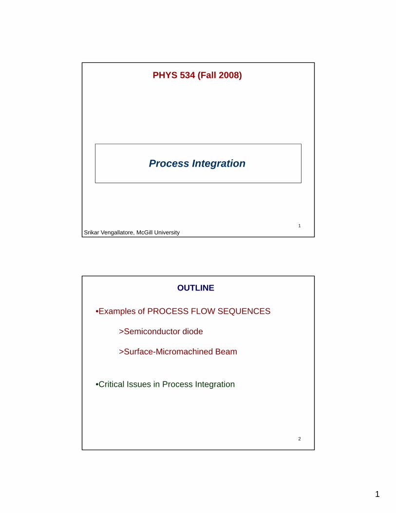
Process Integration
Efficient and cost-effective sequencing of unit processes
to manufacture and package microscale structures and
devices to meet specified performance and reliability targets
3
Process Flow for a Diode
SiO22
Aln+ implant layerp+ implant layer
p-type Si substrate
4[Senturia]

3
SiO2
Aln+ implant layerp+ implant layer
p-type Si substrate
Implant n+
p yp
Metallization
5
Implant p+
Detailed Process Flow for a Diode
Starting Material: (100)-oriented, single-crystal silicon, double-side polished; p-type (1015 /cm3 boron)
Front Side
Reverse Side
6
Step 1 Clean Standard RCA cleans with HF dip
(Back-side)

4
Cleaning is an Art
RCA Cleans are standard.
Step 1: Sulfuric acid and Hydrogen peroxide (7:3)(Removes all organic coatings)
Step 2: Water: Hydrogen peroxide: Ammonium hydroxide (5:1:1)(Removes all organic residues)
Step 3: Water: HCl: Hydrogen peroxide (6:1:1)(Removes all ionic contaminants)
( g g )
7•RCA: Radio Corporation of America
•Need RCA Cleans before every high-temperature step(oxidation, diffusion, or CVD)
Dip in Hydrofluoric Acid (HF) after RCA Cleans
•Silicon has a very strong tendency to oxidize
•When Si is exposed to oxygen, a thin SiO2 layer is formed2This oxide is referred to as Native Oxide
•If the native oxide must be removed, then dip the siliconwafer in HF for a few minutes
St 1
8
“RCA Cleans + HF Dip”Step 1:

5
Step 2 Oxidation
Grow 0.1 μm SiO2 on both surfaces
Choice: wet or dry?
p-Si substrate
SiO2
9
Step 3 Protect front
Spin photoresist on front side and prebakeProtect front surface from contamination during implantation
Step 4 Ion implantImplant boron. Target: 1019/cm3 after all thermal annealing
Back surface
10

6
Si substrate
SiO2
Step 5 Strip photoresist from front surface
Front surface
2
p+ implant layer
11
Step 6 Photolithography
Spin cast resist, prebake, expose top surface using Mask 1. Develop, post-bake.
Mask 1 (implant)
Process parameters: Characteristics of mask aligner
12
Type of photoresist (positive vs. negative)
Exposure time
Development time

7
Structure after photolithographic patterning:
Si substrate
SiO2
p+ implant layer
Photoresist
13
Step 7 Implantation
Ion implant phosphorous. Target = 1019/cm3 after all thermal treatments
SiO2
p+ implant layerPhotoresist
n+ implant layer
14
n+ implant layer

8
SiO2
p+ implant layerPhotoresistn+ implant layer
After Step 7:
n implant layer
Step 8 Remove photoresist from front surface (acetone dip, followed by oxygen plasma)
15
Note: Front surface implanted region cannot be identified using visual inspection !
Step 9 Clean RCA Cleans without HF dip
Step 10 Drive-in Thermal treatment to achieve desired implant profile
Junction depth
Design Specifications: Junction depth = 1 μmSurface concentration = 1019 /cm3
16
>Sophisticated process modeling tools are availableto estimate process parameters
9
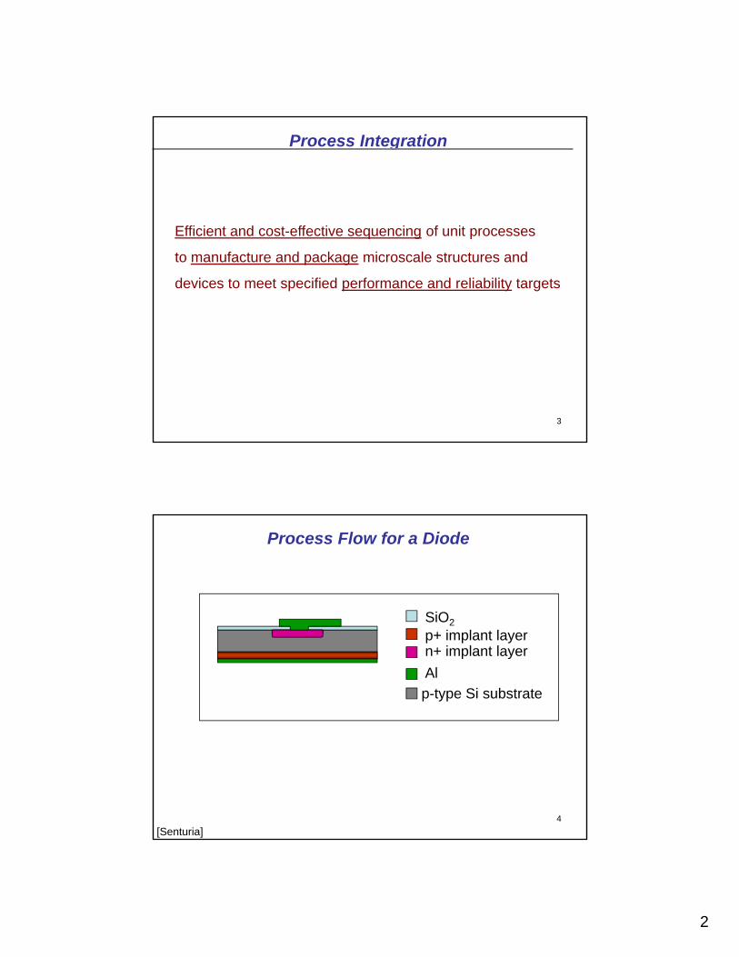
Step 11 Photolithography using Mask 2
Mask 1 (implant) Mask 2 (via)
SiO2
p+ implant layer
Photoresist
17
Photoresistn+ implant layer
Process parameters: ALIGNMENTtype of photoresistExposure & development conditions
Step 12 Etch oxide with buffered HF to open contacts in SiO2
(N t SiO b k f i f ll d i thi )
Step 13: Remove photoresist (acetone + oxygen plasma)
(Note: SiO2 on back-surface is fully removed in this process)
18
10
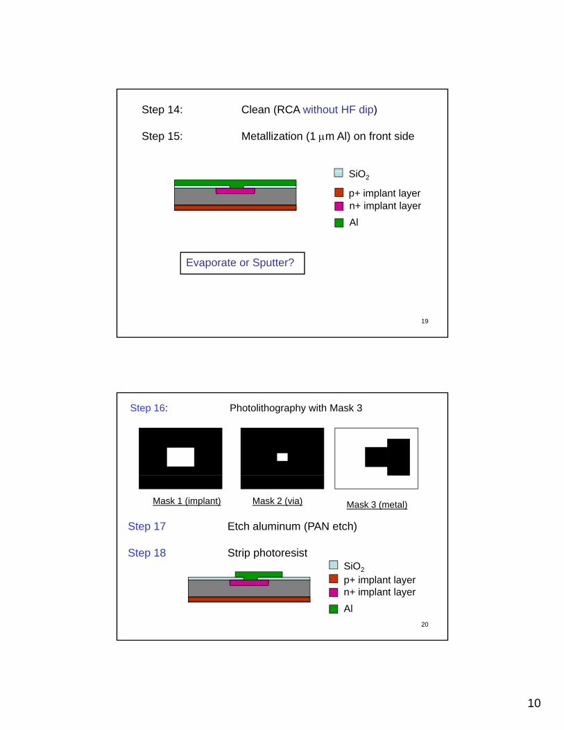
Step 14: Clean (RCA without HF dip)
Step 15: Metallization (1 μm Al) on front side
SiOSiO2
p+ implant layer
Aln+ implant layer
19
Evaporate or Sputter?
Step 16: Photolithography with Mask 3
Mask 1 (implant) Mask 2 (via) Mask 3 (metal)
Step 17 Etch aluminum (PAN etch)
Step 18 Strip photoresist
20
SiO2
Aln+ implant layerp+ implant layer
p p p

11
Step 19 Blanket metal deposition on back surface
SiO2
n+ implant layerp+ implant layer
Aln+ implant layer
21
But, what about PACKAGING?
Step 20: Die saw (separate individual chips)
W f
6-inch 1 mm
Chi
Die-saw
22
Wafer Chip

12
Step 21: Attach bottom metal to ceramic packageWire bond to front surface Al pad.
23(CMC)
Metallization
ChipAluminumBond pad
24(www.unitekeapro.com; www.semlab.com)
13
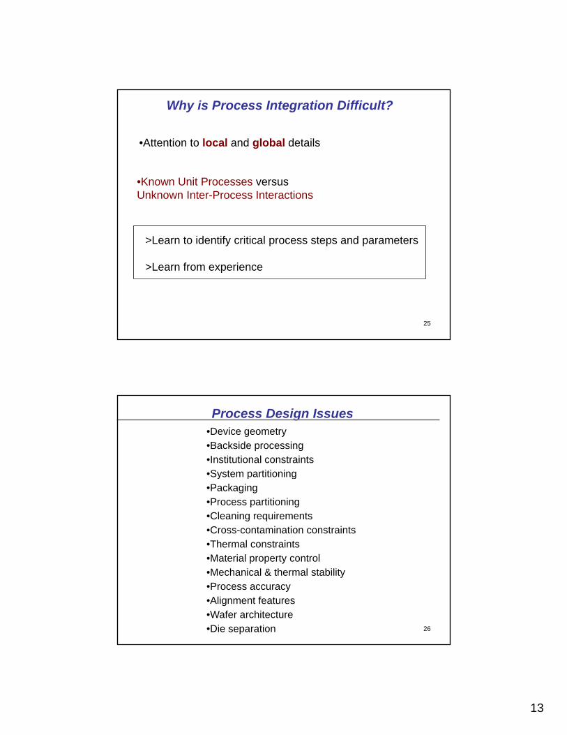
Why is Process Integration Difficult?
•Attention to local and global details
•Known Unit Processes versus Unknown Inter-Process Interactions
>Learn to identify critical process steps and parameters
25
>Learn from experience
Process Design Issues•Device geometry•Backside processing•Institutional constraints•System partitioningy p g•Packaging•Process partitioning•Cleaning requirements•Cross-contamination constraints•Thermal constraints•Material property control
26
p p y•Mechanical & thermal stability•Process accuracy•Alignment features•Wafer architecture•Die separation
14
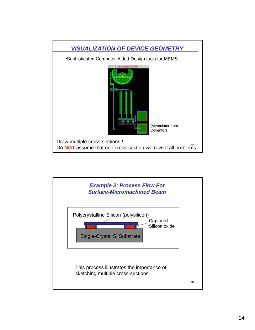
VISUALIZATION OF DEVICE GEOMETRY•Sophisticated Computer-Aided-Design tools for MEMS
27
(Memulator fromCoventor)
Draw multiple cross-sections !Do NOT assume that one cross-section will reveal all problems
Example 2: Process Flow For Surface-Micromachined Beam
Polycrystalline Silicon (polysilicon)CapturedSilicon oxide
Polycrystalline Silicon (polysilicon)
Single-Crystal Si Substrate
28
This process illustrates the importance of sketching multiple cross-sections
15
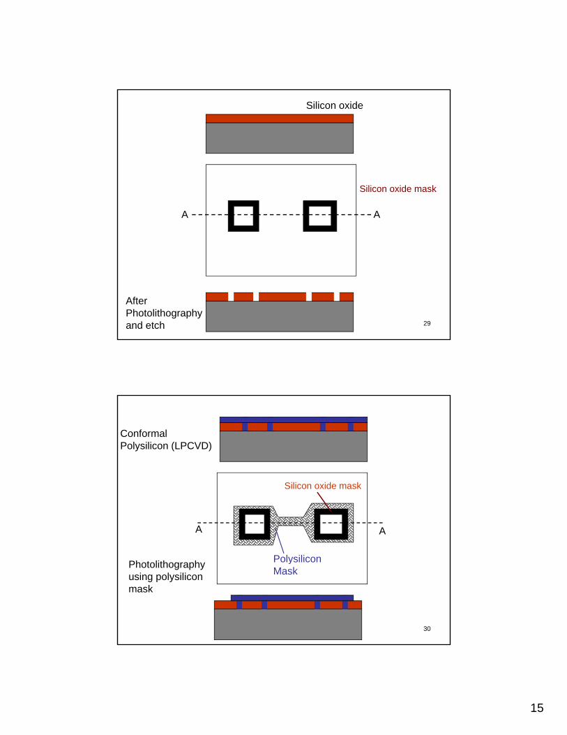
Silicon oxide
Silicon oxide mask
A A
29
AfterPhotolithographyand etch
ConformalPolysilicon (LPCVD)
Polysilicon
Silicon oxide mask
A A
Ph t lith h
30
PolysiliconMaskPhotolithography
using polysilicon mask

16
Release etch
31
Silicon oxide mask
A A
B
Polysiliconmask
A A
B
32Cross-section A-A Cross-section B-B

17
Packaging Microelectronic Devices
•Goals:-Protect chip from environment-Provide electrical connectivity-Provide heat flow path(Modern ICs dissipate enormous power)
•Standard Approach:
-Dice up wafer using die-saw
-Use standard ceramic/plastic packages (commercially available)
33
Use standard ceramic/plastic packages (commercially available)
-Consideration of packaging-induced stresses can be important
•Need multiple interconnections -Fluidic-Electrical-Optical
Packaging MEMS
•Interaction with environment can be critical (ex: pressure sensors)
•Costly! (35% Silicon chip; 45% package; 20% calibration & test)
Disposable blood
34(Motorola)
pressure sensors

18
Au wire bonds
10
35
Polysilicon beams
10 μm
Currently being commercialized: www.polychromix.com
Die Separation
•Die-sawing is a violent operation (wet & dirty)
•Excellent for microelectronics (no-moving parts)
36
Excellent for microelectronics (no moving parts)
•Die-saw can cause micromechanical structures to fracture
•One solution: encapsulate moving parts during die-saw
19
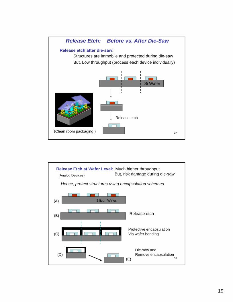
Release Etch: Before vs. After Die-Saw
Release etch after die-saw:Structures are immobile and protected during die-sawBut, Low throughput (process each device individually)
Si Wafer
37
Release etch
(Clean room packaging!)
Release Etch at Wafer Level: Much higher throughputBut, risk damage during die-saw
Hence, protect structures using encapsulation schemes
(Analog Devices)
Silicon Wafer
Release etch
Protective encapsulation
(A)
(B)
38
pVia wafer bonding
Die-saw and Remove encapsulation
(C)
(D)(E)
20
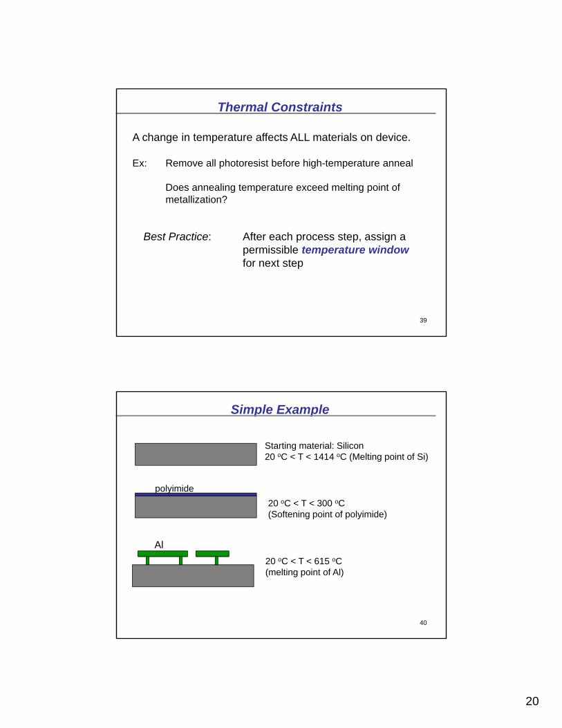
Thermal Constraints
A change in temperature affects ALL materials on device.
Ex: Remove all photoresist before high-temperature anneal
Does annealing temperature exceed melting point of metallization?
Best Practice: After each process step, assign apermissible temperature window
39
p pfor next step
Simple Example
Starting material: Silicon20 oC < T < 1414 oC (Melting point of Si)
polyimide20 oC < T < 300 oC (Softening point of polyimide)
Al
40
20 oC < T < 615 oC (melting point of Al)
21
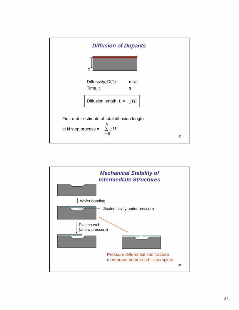
Diffusion of Dopants
x
Diffusivity, D(T) m2/sTime, t s
Diffusion length, L = tD
41
First order estimate of total diffusion length
in N step process = ∑=
N
ntD
0
Mechanical Stability of Intermediate Structures
Wafer bondingWafer bonding
Sealed cavity under pressure
Plasma etch (at low pressure)
42
Pressure differential can fracture membrane before etch is complete

22
Process Accuracy
Variation across wafer (ex: thickness of evaporated metals;DRIE etch rates))
Variation from wafer to wafer (Stress in LPCVD films)
Random variations in process parameters(ex: temperature of tube furnaces; local humidity)
Alignment errors in photolithography
43
Alignment errors in photolithography(especially important in anisotropic wet bulk micromachining)
Depiction of Thin Film Deposition
wH
Perfectly conformal
Non-conformal
h
Perfectly conformal
44
Cuspformation
23
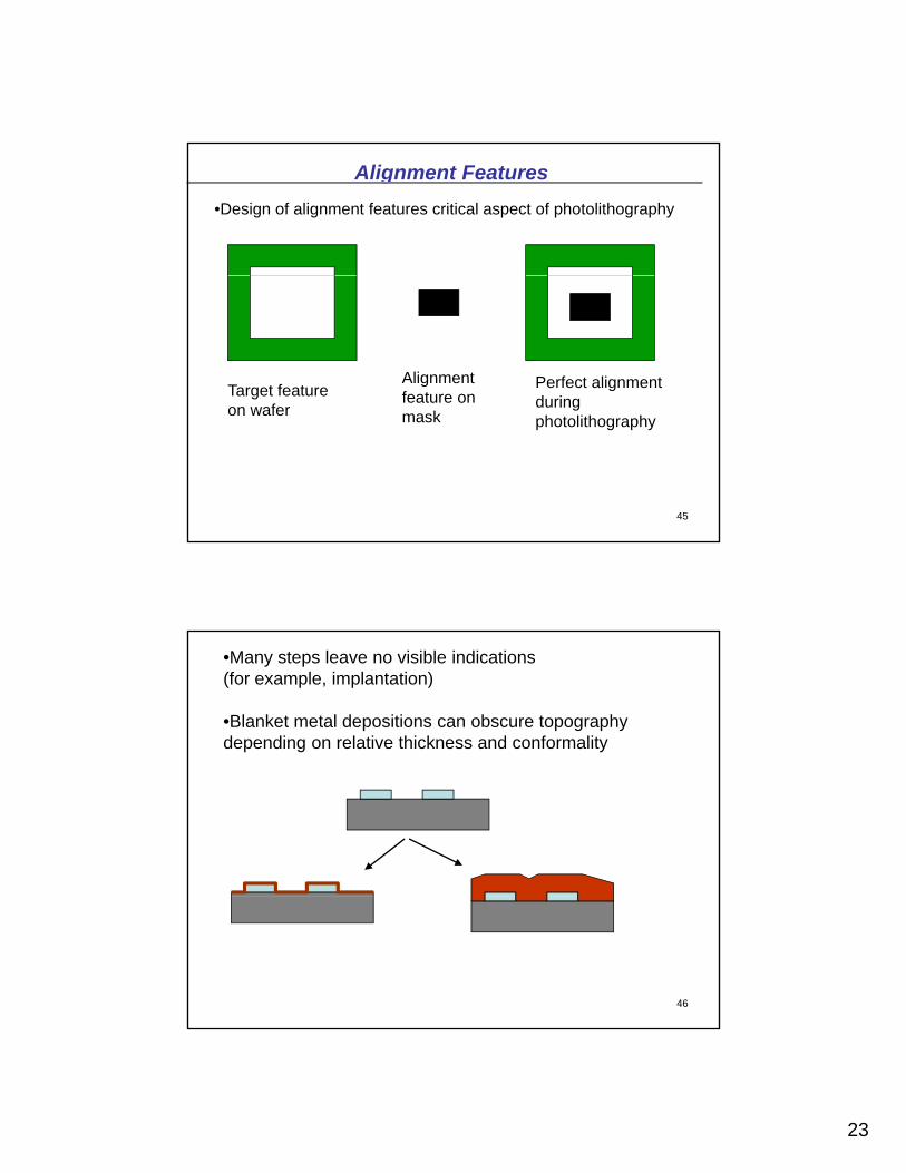
Alignment Features•Design of alignment features critical aspect of photolithography
Target featureon wafer
Alignment feature on
Perfect alignment during
45
on wafer maskg
photolithography
•Many steps leave no visible indications(for example, implantation)
•Blanket metal depositions can obscure topography depending on relative thickness and conformality
46

24
Wafer Architecture •Not all locations on wafer are equivalent
Deep Reactive Ion Etching
Middle of wafer 3 cm away (2.6 %)
42.3 μm 43.4 μm
47
Material Property Control
Residual StressesAffected by temperature;
Strength
Adhesion
Phase stability
ected by te pe atu e;
Local and global details.
48
•Very few predictive models
•Need measurements early in process design!
25
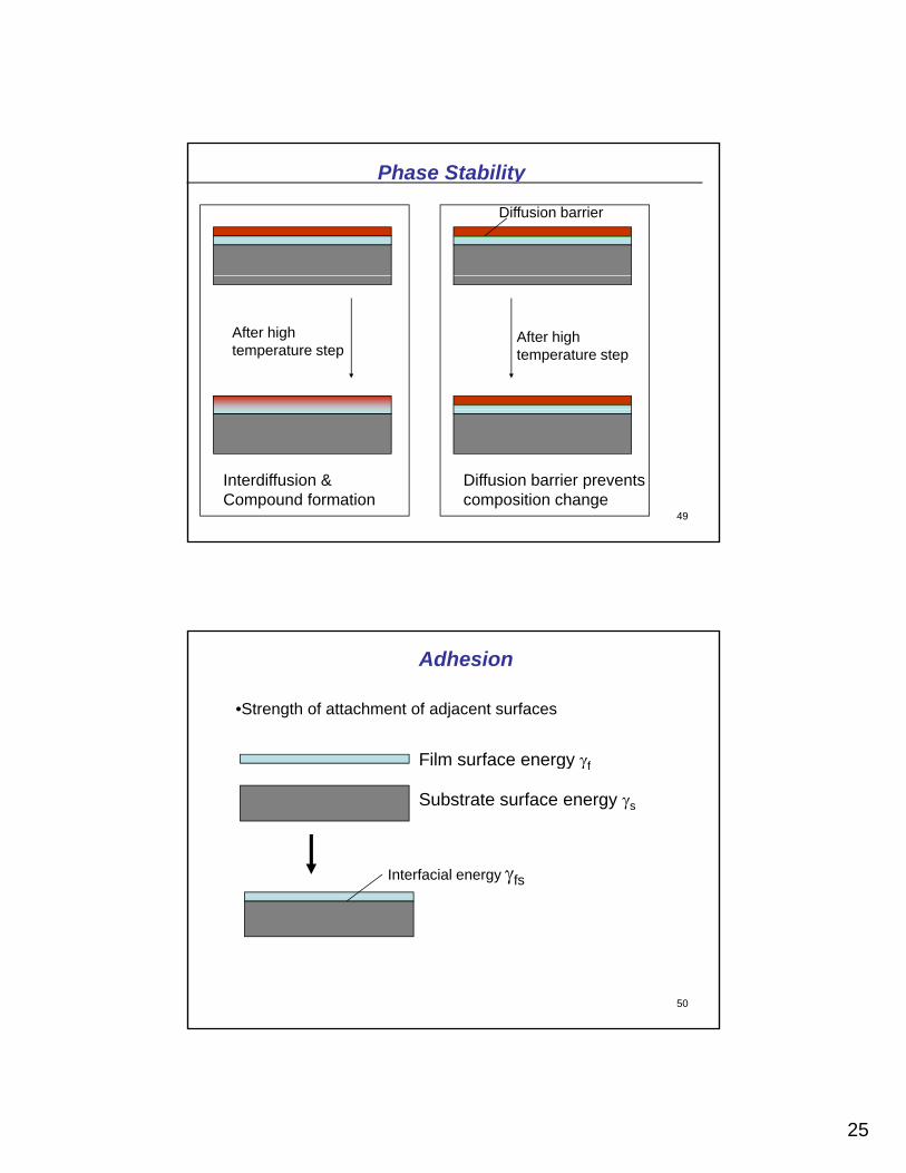
Phase Stability
Diffusion barrier
After high temperature step
After high temperature step
49
Interdiffusion &Compound formation
Diffusion barrier preventscomposition change
Adhesion
•Strength of attachment of adjacent surfaces
Film surface energy γfFilm surface energy γf
Interfacial energy γfs
Substrate surface energy γs
50
26
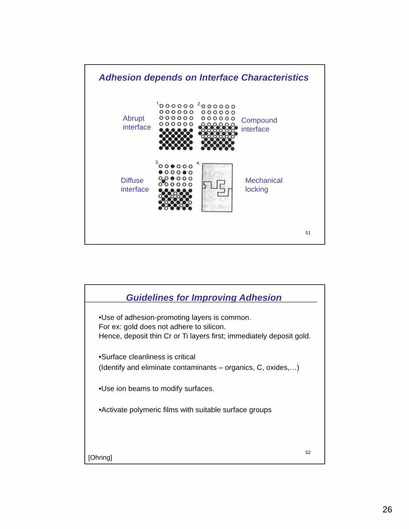
Adhesion depends on Interface Characteristics
Abrupti t f
Compoundinterface interface
Diffuse Mechanical
51
interface locking
Guidelines for Improving Adhesion
•Use of adhesion-promoting layers is common.For ex: gold does not adhere to silicon.Hence, deposit thin Cr or Ti layers first; immediately deposit gold.
•Surface cleanliness is critical(Identify and eliminate contaminants – organics, C, oxides,…)
•Use ion beams to modify surfaces.
52
•Activate polymeric films with suitable surface groups
[Ohring]

27
STRESS CONTROL STRATEGIES
•Explore bulk-micromachining options using stress-free wafers and direct wafer bonding
•Identify sources of stresses (external; thermal; intrinsic)>Thermal stresses: material properties (α); ΔΤ
>Intrinsic stresses: Process selection
53
•If intrinsic stresses cannot be reduced, try stress balancing
STRESS BALANCED STRUCTURES
SUBSTRATE
Compressive layer (σ1, h1)
Tensile layer (σ2, h2)
Condition for zero net stress: 02211 =+ hh σσ
If films are comparable in thickness and stiffness to substrate,then need to negate bending moments as well
54
then need to negate bending moments as well
SUBSTRATE
28
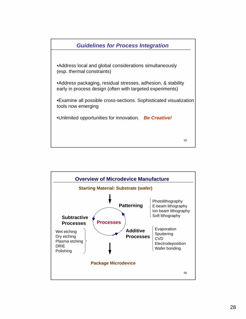
Guidelines for Process Integration
•Address local and global considerations simultaneously(esp. thermal constraints)
•Address packaging, residual stresses, adhesion, & stabilityearly in process design (often with targeted experiments)
•Examine all possible cross-sections. Sophisticated visualizationtools now emerging
55
•Unlimited opportunities for innovation. Be Creative!
Patterning
Starting Material: Substrate (wafer)
Overview of Microdevice Manufacture
PhotolithographyE-beam lithography
Processes
g
Additive Processes
SubtractiveProcesses
EvaporationSputteringCVDElectrodeposition
g p yIon beam lithographySoft lithography
Wet etchingDry etchingPlasma etching
56
Package Microdevice
ElectrodepositionWafer bondingDRIE
Polishing
29
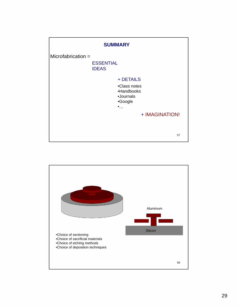
SUMMARY
Microfabrication =ESSENTIALIDEAS
+ DETAILS•Class notes•Handbooks•Journals•Google•
57
+ IMAGINATION!…
Silicon
Aluminum
•Choice of sectioning
58
•Choice of sectioning•Choice of sacrificial materials•Choice of etching methods•Choice of deposition techniques