
AZ - microchemicals.com450CPS).pdf · Through-Silicon-Via (TSV) Advantages to Use a Negative...
23
The information contained herein is, as far as we are aware, true and accurate. However, no representations or warranties, either express or implied, whether of merchantable quality, fitness for any particular purpose or of any other nature are hereby made in respect of the information contained in this presentation or the product or products which are the subject of it. In providing this material, no license or other rights, whether express or implied, are given with respect to any existing or pending patent, patent application, trademarks, or other intellectual property right. AZ ® 15nXT (450 CPS) Photoresist Negative Acting Thick Resist for Cu RDL, TSV, and other plating & etch applications Lithographic and Plating Performance Comparison at 10 μm FT on Cu wafers January 2009
Transcript of AZ - microchemicals.com450CPS).pdf · Through-Silicon-Via (TSV) Advantages to Use a Negative...
The information contained herein is, as far as we are aware, true and accurate. However, no representations or warranties, either express or implied, whether of merchantable quality, fitness for any particular purpose or of any other nature are hereby made in respect of the information contained in this presentation or the product or products which are the subject of it. In providing this material, no license or other rights, whether express or implied, are given with respect to any existing or pending patent, patent application, trademarks, or other intellectual property right.
AZ® 15nXT (450 CPS) Photoresist
Negative Acting Thick Resist for Cu RDL, TSV, and other plating & etch applications
Lithographic and Plating Performance Comparison at 10 µm FT on Cu wafers
January 2009
AZ, the AZ logo, BARLi, Aquatar, nLOF, Kwik Strip, Klebosol, and Spinfil are registered trademarks and AX, DX, HERB, HiR, MiR, NCD, PLP, Signiflow, SWG, and TARP are trademarks of AZ Electronic Materials.
2
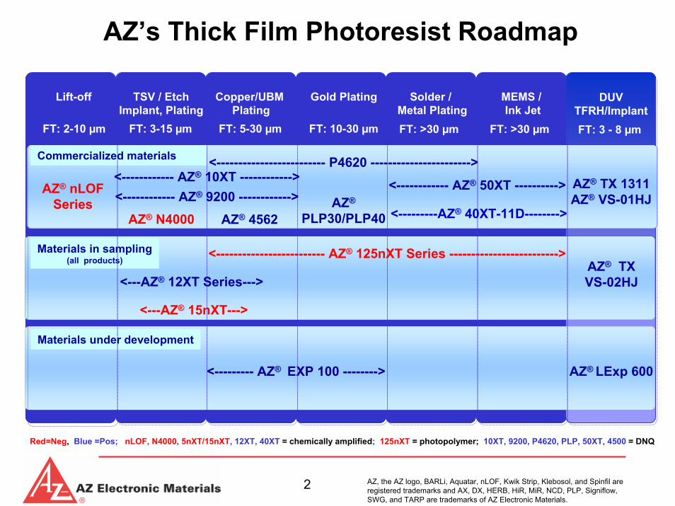
MEMS /Ink Jet
FT: >30 µm
Lift-off TSV / EtchImplant, Plating
Copper/UBMPlating
Gold Plating Solder /Metal Plating
FT: 2-10 µm FT: 3-15 µm FT: 5-30 µm FT: 10-30 µm FT: >30 µm
DUVTFRH/ImplantFT: 3 - 8 µm
AZ’s Thick Film Photoresist Roadmap
<<------------------ AZAZ® EXP 100 EXP 100 ---------------->>
Materials under development
AZ® LExp 600
<---AZ® 12XT Series--->
<------------------------- AZ® 125nXT Series ------------------------->Materials in sampling(all products)
Commercialized materials
AZ® nLOFSeries
<------------------------- P4620 ----------------------->
AZ® N4000
AZ® TX 1311AZ® VS-01HJ<------------ AZ® 9200 ------------> AZ®
PLP30/PLP40
<------------ AZ® 50XT ---------->
<---AZ® 15nXT--->
<---------AZ® 40XT-11D-------->
<------------ AZ® 10XT ------------>
AZ® TXVS-02HJ
AZ® 4562
Red=Neg, Blue =Pos; nLOF, N4000, 5nXT/15nXT, 12XT, 40XT = chemically amplified; 125nXT = photopolymer; 10XT, 9200, P4620, PLP, 50XT, 4500 = DNQ
AZ, the AZ logo, BARLi, Aquatar, nLOF, Kwik Strip, Klebosol, and Spinfil are registered trademarks and AX, DX, HERB, HiR, MiR, NCD, PLP, Signiflow, SWG, and TARP are trademarks of AZ Electronic Materials.
3
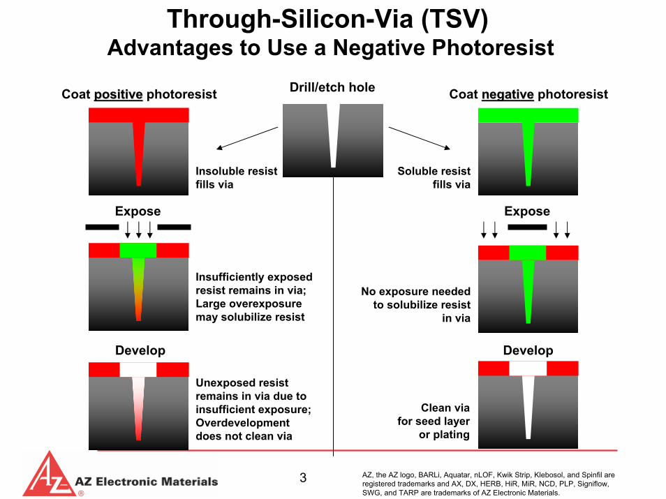
Through-Silicon-Via (TSV)Advantages to Use a Negative Photoresist
Coat positivepositive photoresist
Expose
Develop
Coat negativenegative photoresist
Expose
Develop
Unexposed resist remains in via due to insufficient exposure;Overdevelopmentdoes not clean via
Insufficiently exposedresist remains in via;Large overexposuremay solubilize resist
No exposure neededto solubilize resist
in via
Insoluble resistfills via
Soluble resistfills via
Clean viafor seed layer
or plating
Drill/etch hole
AZ, the AZ logo, BARLi, Aquatar, nLOF, Kwik Strip, Klebosol, and Spinfil are registered trademarks and AX, DX, HERB, HiR, MiR, NCD, PLP, Signiflow, SWG, and TARP are trademarks of AZ Electronic Materials.
4
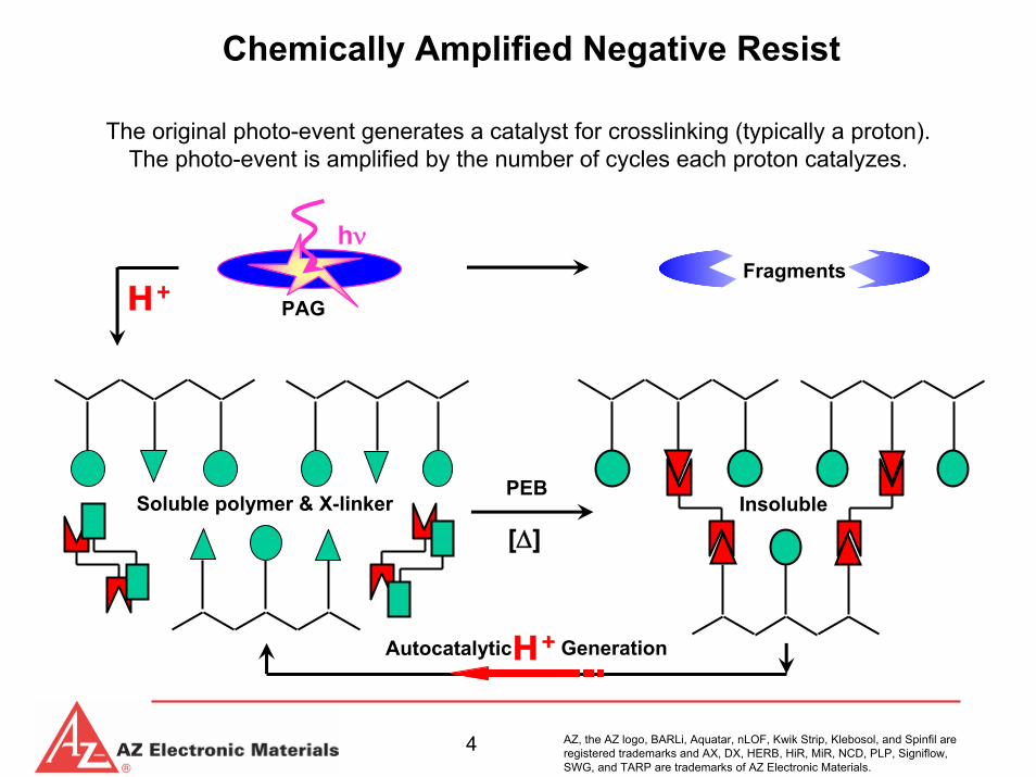
Chemically Amplified Negative Resist
The original photo-event generates a catalyst for crosslinking (typically a proton). The photo-event is amplified by the number of cycles each proton catalyzes.
Fragmentshν
H+
H+Autocatalytic Generation
PAG
Soluble polymer & X-linker InsolublePEB
[Δ]
AZ, the AZ logo, BARLi, Aquatar, nLOF, Kwik Strip, Klebosol, and Spinfil are registered trademarks and AX, DX, HERB, HiR, MiR, NCD, PLP, Signiflow, SWG, and TARP are trademarks of AZ Electronic Materials.
5
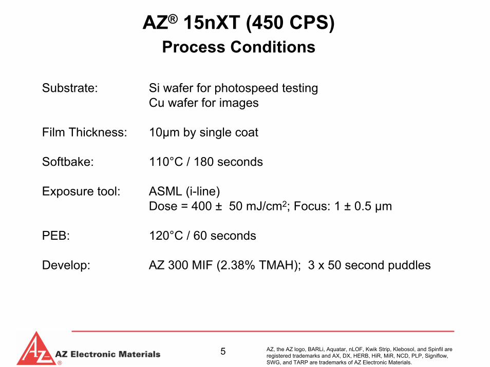
AZ® 15nXT (450 CPS)Process Conditions
Substrate: Si wafer for photospeed testingCu wafer for images
Film Thickness: 10µm by single coat
Softbake: 110°C / 180 seconds
Exposure tool: ASML (i-line)Dose = 400 ± 50 mJ/cm2; Focus: 1 ± 0.5 µm
PEB: 120°C / 60 seconds
Develop: AZ 300 MIF (2.38% TMAH); 3 x 50 second puddles
AZ, the AZ logo, BARLi, Aquatar, nLOF, Kwik Strip, Klebosol, and Spinfil are registered trademarks and AX, DX, HERB, HiR, MiR, NCD, PLP, Signiflow, SWG, and TARP are trademarks of AZ Electronic Materials.
6
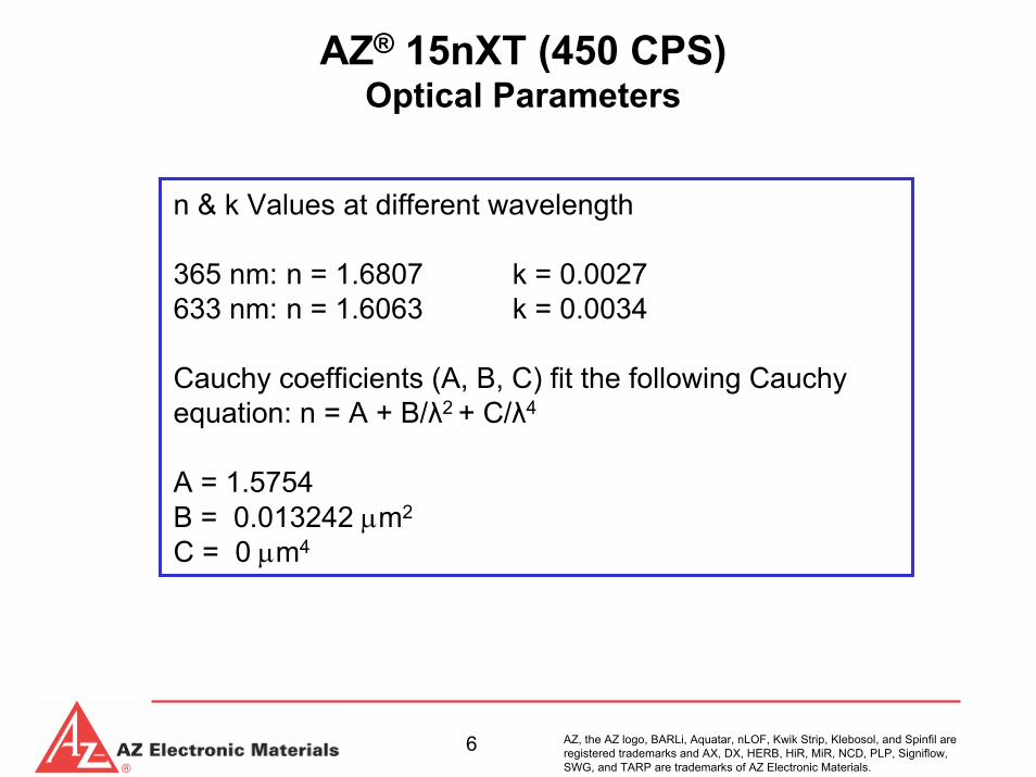
AZ® 15nXT (450 CPS) Optical Parameters
n & k Values at different wavelength
365 nm: n = 1.6807 k = 0.0027633 nm: n = 1.6063 k = 0.0034
Cauchy coefficients (A, B, C) fit the following Cauchy equation: n = A + B/λ2 + C/λ4
A = 1.5754B = 0.013242 μm2
C = 0 μm4
AZ, the AZ logo, BARLi, Aquatar, nLOF, Kwik Strip, Klebosol, and Spinfil are registered trademarks and AX, DX, HERB, HiR, MiR, NCD, PLP, Signiflow, SWG, and TARP are trademarks of AZ Electronic Materials.
7
4
6
8
10
12
14
16
18
20
22
24
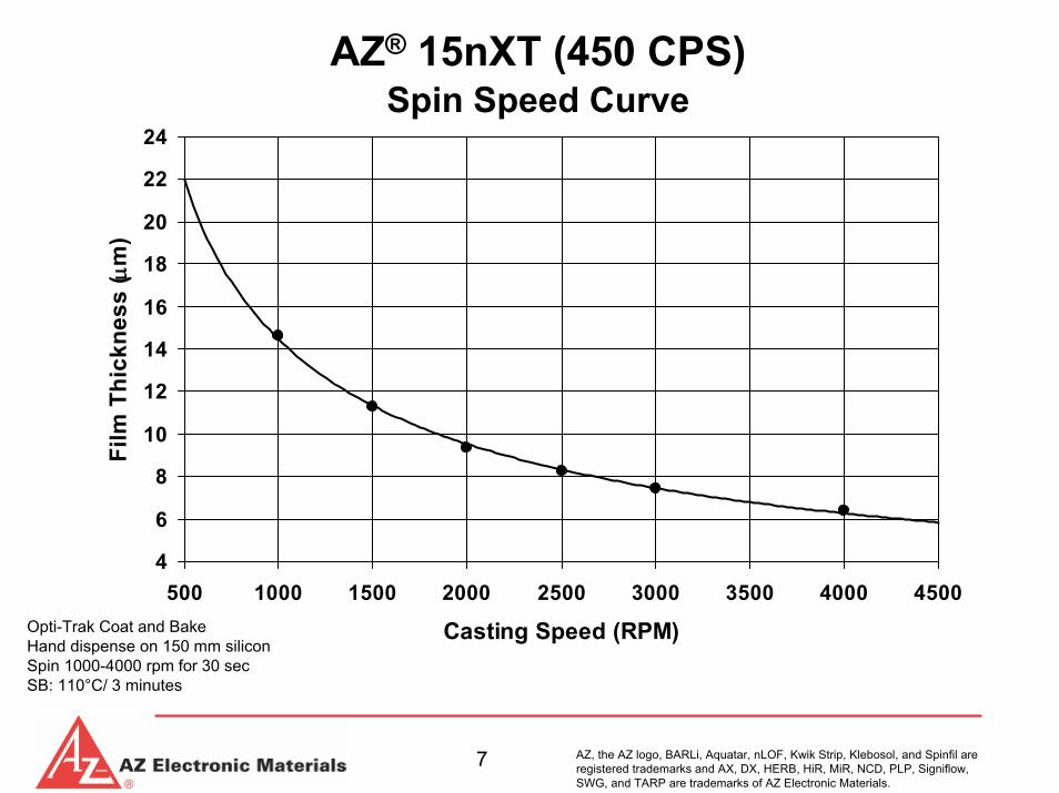
500 1000 1500 2000 2500 3000 3500 4000 4500
Casting Speed (RPM)
Film
Thi
ckne
ss ( μ
m)
Opti-Trak Coat and BakeHand dispense on 150 mm siliconSpin 1000-4000 rpm for 30 secSB: 110°C/ 3 minutes
AZ® 15nXT (450 CPS)Spin Speed Curve
AZ, the AZ logo, BARLi, Aquatar, nLOF, Kwik Strip, Klebosol, and Spinfil are registered trademarks and AX, DX, HERB, HiR, MiR, NCD, PLP, Signiflow, SWG, and TARP are trademarks of AZ Electronic Materials.
8
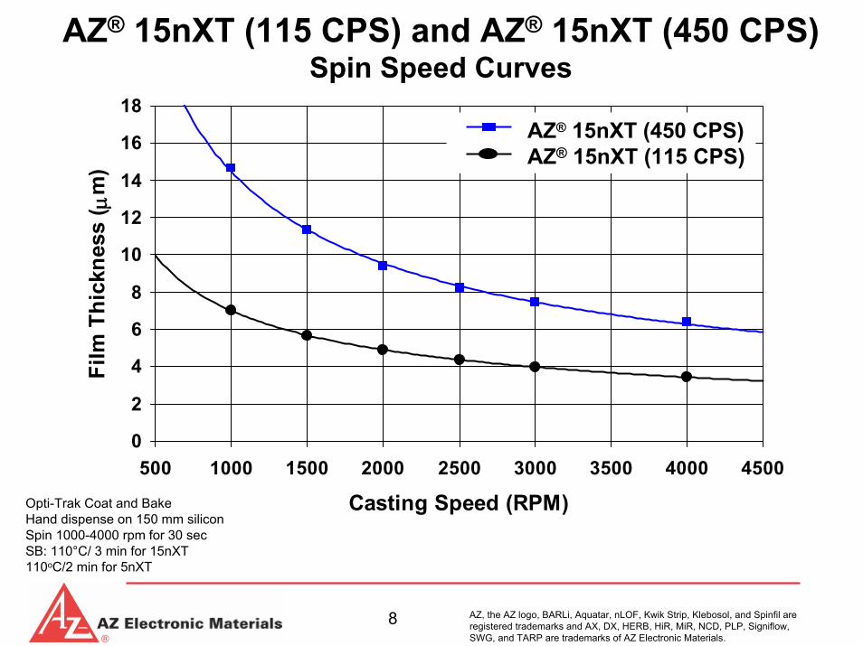
AZ® 15nXT (115 CPS) and AZ® 15nXT (450 CPS)Spin Speed Curves
Opti-Trak Coat and BakeHand dispense on 150 mm siliconSpin 1000-4000 rpm for 30 secSB: 110°C/ 3 min for 15nXT 110oC/2 min for 5nXT
0
2
4
6
8
10
12
14
16
18
500 1000 1500 2000 2500 3000 3500 4000 4500
Casting Speed (RPM)
Film
Thi
ckne
ss ( μ
m)
AZ® 15nXT (450 CPS)AZ® 15nXT (115 CPS)
AZ, the AZ logo, BARLi, Aquatar, nLOF, Kwik Strip, Klebosol, and Spinfil are registered trademarks and AX, DX, HERB, HiR, MiR, NCD, PLP, Signiflow, SWG, and TARP are trademarks of AZ Electronic Materials.
9
0.0 μm
0.5 μm
1.0 μm
1.5 μm
2.0 μm
2.5 μm
10µm 5µmAZ® 15nXT (450 CPS)Depth of Focus
AZ, the AZ logo, BARLi, Aquatar, nLOF, Kwik Strip, Klebosol, and Spinfil are registered trademarks and AX, DX, HERB, HiR, MiR, NCD, PLP, Signiflow, SWG, and TARP are trademarks of AZ Electronic Materials.
10
3.6 µm
10 µm 4.5 µm5 µm
4 µm3.4 µm
400 mJ/cm2, F = 1 µm
AZ® 15nXT (450 CPS)Linearity, Resolution
AZ, the AZ logo, BARLi, Aquatar, nLOF, Kwik Strip, Klebosol, and Spinfil are registered trademarks and AX, DX, HERB, HiR, MiR, NCD, PLP, Signiflow, SWG, and TARP are trademarks of AZ Electronic Materials.
11
300 mJ/cm2 350 mJ/cm2
400 mJ/cm2
450 mJ/cm2500 mJ/cm2550 mJ/cm2
250 mJ/cm2
Film Thickness: 10μmOpti Track Coat and BakeSB: 110°C/3 minutesASML i-Line Stepper, F= +1.0μmOpti Track PEB/DevelopPEB: 120°C/ 60 SecondsAZ 300 MIF/ 3x50sec Spray/Puddle @23°C
AZ® 15nXT (450 CPS) - Exposure LatitudeFT = 10 μm, Focus = 1.0 μm, 5.0 μm L/S on Cu Wafers
AZ, the AZ logo, BARLi, Aquatar, nLOF, Kwik Strip, Klebosol, and Spinfil are registered trademarks and AX, DX, HERB, HiR, MiR, NCD, PLP, Signiflow, SWG, and TARP are trademarks of AZ Electronic Materials.
12
4
4.5
5
5.5
6
150 175 200 225 250 275 300 325 350 375 400 425 450 475 500Exposure Dose (mJ/cm2)
Mea
sure
d Li
ne W
idth
(µm
)
AZ® 15nXT (450 CPS) - Exposure LatitudeFT = 10 μm, Focus = 1.0 μm, 5.0 μm L/S on Cu Wafers
Film Thickness: 10μmOpti Track Coat and BakeSB: 110°C/3 minutesASML i-Line Stepper, F= +1.0μmOpti Track PEB/DevelopPEB: 120°C/ 60 SecondsAZ 300 MIF/ 3x50sec Spray/Puddle @23°C
AZ, the AZ logo, BARLi, Aquatar, nLOF, Kwik Strip, Klebosol, and Spinfil are registered trademarks and AX, DX, HERB, HiR, MiR, NCD, PLP, Signiflow, SWG, and TARP are trademarks of AZ Electronic Materials.
13
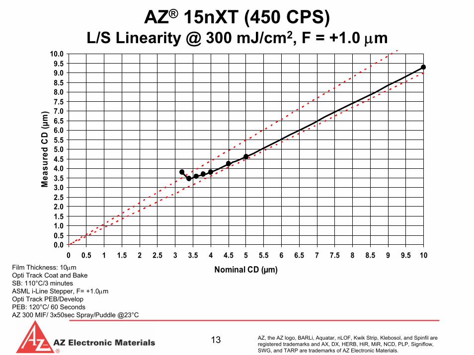
AZ® 15nXT (450 CPS)L/S Linearity @ 300 mJ/cm2, F = +1.0 μm
0.00.51.01.52.02.53.03.54.04.55.05.56.06.57.07.58.08.59.09.5
10.0
0 0.5 1 1.5 2 2.5 3 3.5 4 4.5 5 5.5 6 6.5 7 7.5 8 8.5 9 9.5 10
Nominal CD (µm)
Mea
sure
d C
D (µ
m)
Film Thickness: 10μmOpti Track Coat and BakeSB: 110°C/3 minutesASML i-Line Stepper, F= +1.0μmOpti Track PEB/DevelopPEB: 120°C/ 60 SecondsAZ 300 MIF/ 3x50sec Spray/Puddle @23°C
AZ, the AZ logo, BARLi, Aquatar, nLOF, Kwik Strip, Klebosol, and Spinfil are registered trademarks and AX, DX, HERB, HiR, MiR, NCD, PLP, Signiflow, SWG, and TARP are trademarks of AZ Electronic Materials.
14
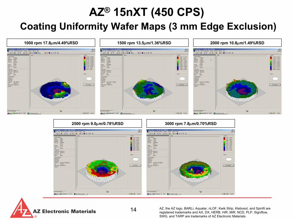
AZ® 15nXT (450 CPS)Coating Uniformity Wafer Maps (3 mm Edge Exclusion)
1000 rpm 17.8μm/4.49%RSD 1500 rpm 13.5μm/1.36%RSD 2000 rpm 10.8μm/1.49%RSD
2500 rpm 9.0μm/0.78%RSD 3000 rpm 7.8μm/0.70%RSD
AZ, the AZ logo, BARLi, Aquatar, nLOF, Kwik Strip, Klebosol, and Spinfil are registered trademarks and AX, DX, HERB, HiR, MiR, NCD, PLP, Signiflow, SWG, and TARP are trademarks of AZ Electronic Materials.
15
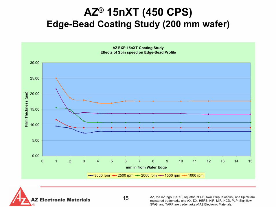
AZ® 15nXT (450 CPS)Edge-Bead Coating Study (200 mm wafer)
AZ EXP 15nXT Coating StudyEffects of Spin speed on Edge-Bead Profile
0.00
5.00
10.00
15.00
20.00
25.00
30.00
0 1 2 3 4 5 6 7 8 9 10 11 12 13 14 15
mm in from Wafer Edge
Film
Thi
ckne
ss (µ
m)
3000 rpm 2500 rpm 2000 rpm 1500 rpm 1000 rpm
AZ, the AZ logo, BARLi, Aquatar, nLOF, Kwik Strip, Klebosol, and Spinfil are registered trademarks and AX, DX, HERB, HiR, MiR, NCD, PLP, Signiflow, SWG, and TARP are trademarks of AZ Electronic Materials.
16
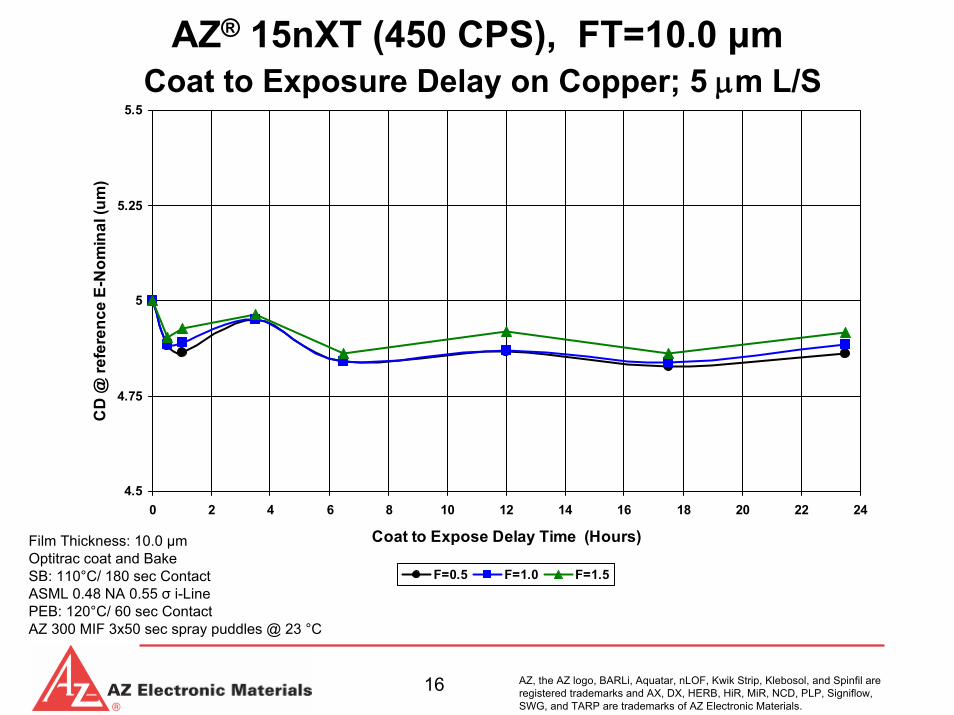
AZ® 15nXT (450 CPS), FT=10.0 μm Coat to Exposure Delay on Copper; 5 μm L/S
4.5
4.75
5
5.25
5.5
0 2 4 6 8 10 12 14 16 18 20 22 24
Coat to Expose Delay Time (Hours)
CD
@ re
fere
nce
E-N
omin
al (u
m)
F=0.5 F=1.0 F=1.5
Film Thickness: 10.0 µmOptitrac coat and BakeSB: 110°C/ 180 sec ContactASML 0.48 NA 0.55 σ i-LinePEB: 120°C/ 60 sec ContactAZ 300 MIF 3x50 sec spray puddles @ 23 °C

AZ, the AZ logo, BARLi, Aquatar, nLOF, Kwik Strip, Klebosol, and Spinfil are registered trademarks and AX, DX, HERB, HiR, MiR, NCD, PLP, Signiflow, SWG, and TARP are trademarks of AZ Electronic Materials.
17
Film Thickness: 10.0 µmOptitrac coat and BakeSB: 110°C/ 180 sec ContactASML 0.48 NA 0.55 σ i-LinePEB: 120°C/ 60 sec ContactAZ 300 MIF 3x50 sec spray puddles @ 23 °C
AZ® 15nXT (450 CPS) , F = +1.0 µm, FT=10.0 μm Coat to Exposure Delay on Copper (hr:mm); 5 μm L/S
4.0
4.3
4.5
4.8
5.0
5.3
5.5
5.8
6.0
150 200 250 300 350 400 450 500 550
Dose (mJ/cm2)
Mea
sure
d C
D ( μ
m) 23:35 Hrs
17:25 Hrs12:00 Hrs6:30 Hrs3:35 Hrs1:00 Hrs0:30 hrs0:01 Hrs
AZ, the AZ logo, BARLi, Aquatar, nLOF, Kwik Strip, Klebosol, and Spinfil are registered trademarks and AX, DX, HERB, HiR, MiR, NCD, PLP, Signiflow, SWG, and TARP are trademarks of AZ Electronic Materials.
18
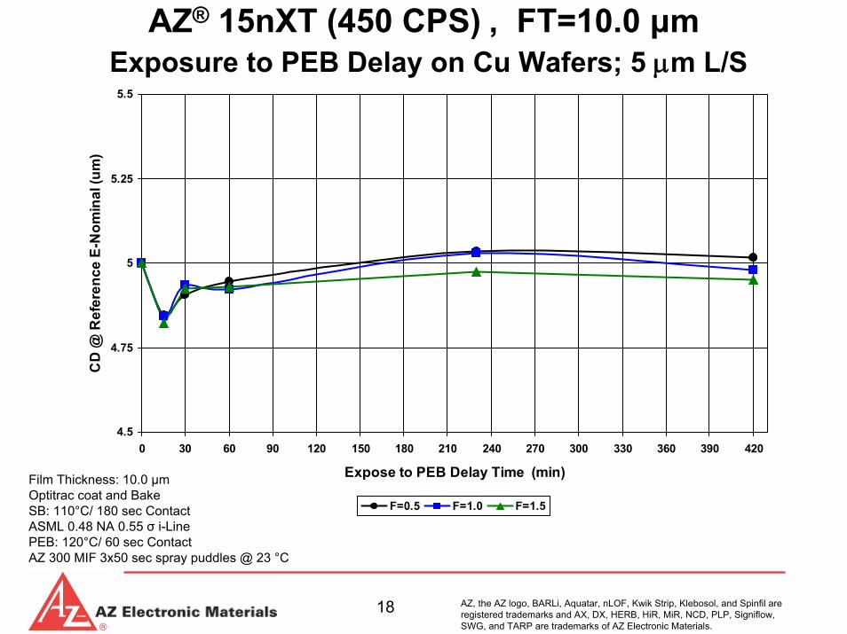
AZ® 15nXT (450 CPS) , FT=10.0 μm Exposure to PEB Delay on Cu Wafers; 5 μm L/S
4.5
4.75
5
5.25
5.5
0 30 60 90 120 150 180 210 240 270 300 330 360 390 420
Expose to PEB Delay Time (min)
CD
@ R
efer
ence
E-N
omin
al (u
m)
F=0.5 F=1.0 F=1.5
Film Thickness: 10.0 µmOptitrac coat and BakeSB: 110°C/ 180 sec ContactASML 0.48 NA 0.55 σ i-LinePEB: 120°C/ 60 sec ContactAZ 300 MIF 3x50 sec spray puddles @ 23 °C
AZ, the AZ logo, BARLi, Aquatar, nLOF, Kwik Strip, Klebosol, and Spinfil are registered trademarks and AX, DX, HERB, HiR, MiR, NCD, PLP, Signiflow, SWG, and TARP are trademarks of AZ Electronic Materials.
19
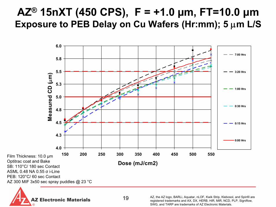
Film Thickness: 10.0 µmOptitrac coat and BakeSB: 110°C/ 180 sec ContactASML 0.48 NA 0.55 σ i-LinePEB: 120°C/ 60 sec ContactAZ 300 MIF 3x50 sec spray puddles @ 23 °C
AZ® 15nXT (450 CPS), F = +1.0 µm, FT=10.0 μmExposure to PEB Delay on Cu Wafers (Hr:mm); 5 μm L/S
4.0
4.3
4.5
4.8
5.0
5.3
5.5
5.8
6.0
150 200 250 300 350 400 450 500 550
Dose (mJ/cm2)
Mea
sure
d C
D ( μ
m)
7:00 Hrs
3:20 Hrs
1:00 Hrs
0:30 Hrs
0:15 Hrs
0:00 Hrs
AZ, the AZ logo, BARLi, Aquatar, nLOF, Kwik Strip, Klebosol, and Spinfil are registered trademarks and AX, DX, HERB, HiR, MiR, NCD, PLP, Signiflow, SWG, and TARP are trademarks of AZ Electronic Materials.
20
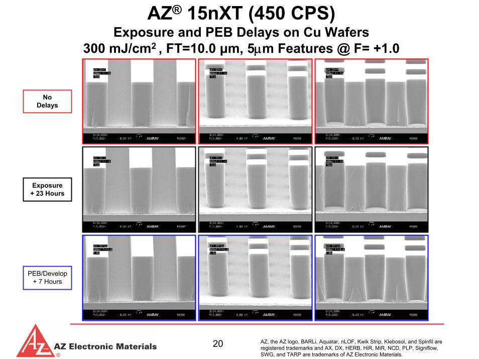
AZ® 15nXT (450 CPS)Exposure and PEB Delays on Cu Wafers
300 mJ/cm2 , FT=10.0 μm, 5μm Features @ F= +1.0
NoDelays
Exposure+ 23 Hours
PEB/Develop+ 7 Hours
AZ, the AZ logo, BARLi, Aquatar, nLOF, Kwik Strip, Klebosol, and Spinfil are registered trademarks and AX, DX, HERB, HiR, MiR, NCD, PLP, Signiflow, SWG, and TARP are trademarks of AZ Electronic Materials.
21
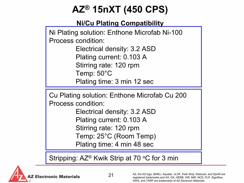
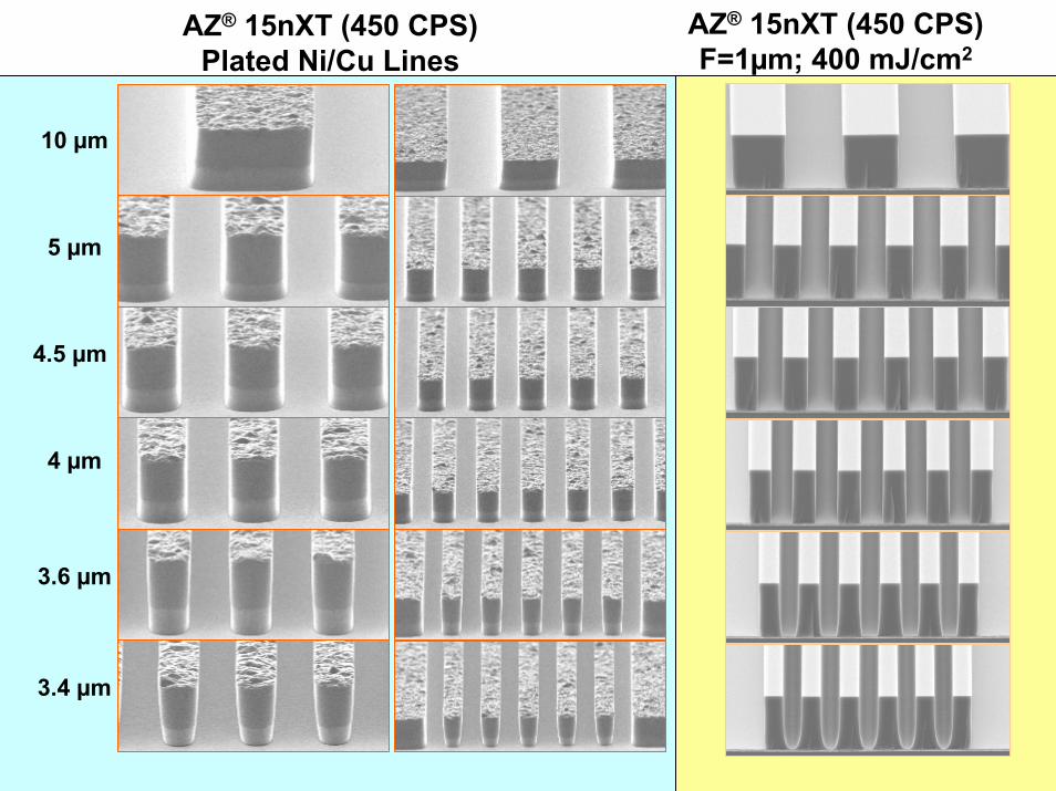
Ni Plating solution: Enthone Microfab Ni-100Process condition:
Electrical density: 3.2 ASDPlating current: 0.103 A Stirring rate: 120 rpmTemp: 50°CPlating time: 3 min 12 sec
AZ® 15nXT (450 CPS)Ni/Cu Plating Compatibility
Cu Plating solution: Enthone Microfab Cu 200Process condition:
Electrical density: 3.2 ASDPlating current: 0.103 A Stirring rate: 120 rpmTemp: 25°C (Room Temp)Plating time: 4 min 48 sec
Stripping: AZ® Kwik Strip at 70 oC for 3 min
AZ, the AZ logo, BARLi, Aquatar, nLOF, Kwik Strip, Klebosol, and Spinfil are registered trademarks and AX, DX, HERB, HiR, MiR, NCD, PLP, Signiflow, SWG, and TARP are trademarks of AZ Electronic Materials.
22
AZ® 15nXT (450 CPS)F=1µm; 400 mJ/cm2
3.6 µm
10 µm
4.5 µm
5 µm
4 µm
3.4 µm
AZ® 15nXT (450 CPS) Plated Ni/Cu Lines
AZ, the AZ logo, BARLi, Aquatar, nLOF, Kwik Strip, Klebosol, and Spinfil are registered trademarks and AX, DX, HERB, HiR, MiR, NCD, PLP, Signiflow, SWG, and TARP are trademarks of AZ Electronic Materials.
23
AZ® 15nXT (450 CPS)Summary
Compatible on Cu type substrates and other metals.Very good lithographic throughput; very competitive photospeed and develop time.Excellent adhesion, no underplating.Vertical sidewall profiles.Wide compatibility to plating solutions, including Cu, Ni, and Au.Easily strips after plating; stripped completely in AZ Kwik Strip at 70°C for 3 min.Very good stability and shelf lifeThinner version available for lower FT range; 15nXT (115 CPS).


![Negative-tone Cycloolefin Photoresist for 193 nm Lithographyntur.lib.ntu.edu.tw/bitstream/246246/148174/1/33.pdfCOOH]. EA: C, 71.65; H, 7.71 (caic. C, 71.07; H, 7.89). Thermal decomposition](https://static.fdocuments.in/doc/165x107/5fb4e94e2f9e462cdc023c07/negative-tone-cycloolefin-photoresist-for-193-nm-cooh-ea-c-7165-h-771-caic.jpg)
