PHOTONIC CRYSTALS & METAMATERIAL FILTERS BASED ON …jpier.org/PIER/pier113/11.10122501.pdf ·...
16
Progress In Electromagnetics Research, Vol. 113, 179–194, 2011 PHOTONIC CRYSTALS & METAMATERIAL FILTERS BASED ON 2D ARRAYS OF SILICON NANOPILLARS H. Butt, Q. Dai, and T. D. Wilkinson † Centre of Molecular Materials for Photonics & Electronics Department of Engineering, University of Cambridge 9 J. J. Thomson Avenue, Cambridge CB3 0FA, United Kingdom G. A. J. Amaratunga Electronics, Power and Energy Conversion Group Department of Engineering, University of Cambridge 9 J. J. Thomson Avenue, Cambridge CB3 0FA, United Kingdom Abstract—Highly dense two-dimensional periodic arrays of nano- scaled silicon pillars present interesting photonic band gaps and the capacity to act as photonic crystals which can mould, manipulate and guide light. We demonstrate finite element modelling of silicon pillars based photonic crystals and their effective use in applications like waveguides, optical power dividers, multiplexers and switches. The optical wave propagation through these structures was thoroughly simulated and analysed, confirming their high efficiency. The band gaps studied through the plane wave expansion method are also presented. Later the fabrication of highly periodic two-dimensional arrays of silicon pillars through the process of etching is also explained. The arrays with pillar radius of 50 nm and lattice constant of 400 nm were successfully utilised as photonic crystal waveguides and their measured results are reported. Moreover, the silicon nanopillars sputtered with noble metals can also display artificial optical properties and act as metamaterials due to the mutual plasmonic coupling effects. We report the theoretical results for the silicon nanopillars based metamaterial high-pass filter. Received 25 December 2010, Accepted 14 January 2011, Scheduled 2 February 2011 Corresponding author: Haider Butt ([email protected]). † Haider Butt and Qing Dia contributed equally to this manuscript.
Transcript of PHOTONIC CRYSTALS & METAMATERIAL FILTERS BASED ON …jpier.org/PIER/pier113/11.10122501.pdf ·...

Progress In Electromagnetics Research, Vol. 113, 179–194, 2011
PHOTONIC CRYSTALS & METAMATERIAL FILTERSBASED ON 2D ARRAYS OF SILICON NANOPILLARS
H. Butt, Q. Dai, and T. D. Wilkinson †
Centre of Molecular Materials for Photonics & ElectronicsDepartment of Engineering, University of Cambridge9 J. J. Thomson Avenue, Cambridge CB3 0FA, United Kingdom
G. A. J. Amaratunga
Electronics, Power and Energy Conversion GroupDepartment of Engineering, University of Cambridge9 J. J. Thomson Avenue, Cambridge CB3 0FA, United Kingdom
Abstract—Highly dense two-dimensional periodic arrays of nano-scaled silicon pillars present interesting photonic band gaps and thecapacity to act as photonic crystals which can mould, manipulateand guide light. We demonstrate finite element modelling of siliconpillars based photonic crystals and their effective use in applicationslike waveguides, optical power dividers, multiplexers and switches.The optical wave propagation through these structures was thoroughlysimulated and analysed, confirming their high efficiency. The bandgaps studied through the plane wave expansion method are alsopresented. Later the fabrication of highly periodic two-dimensionalarrays of silicon pillars through the process of etching is also explained.The arrays with pillar radius of 50 nm and lattice constant of 400 nmwere successfully utilised as photonic crystal waveguides and theirmeasured results are reported. Moreover, the silicon nanopillarssputtered with noble metals can also display artificial optical propertiesand act as metamaterials due to the mutual plasmonic coupling effects.We report the theoretical results for the silicon nanopillars basedmetamaterial high-pass filter.
Received 25 December 2010, Accepted 14 January 2011, Scheduled 2 February 2011Corresponding author: Haider Butt ([email protected]).
† Haider Butt and Qing Dia contributed equally to this manuscript.

180 Butt et al.
1. INTRODUCTION
Photonic crystals (PCs) are interesting materials which presentperiodicity in their dielectric constant. Bragg scattering occurswhen the periodicity of the dielectric constant is comparable to thewavelength of the incident electromagnetic waves. This introducesband gaps, which means the electromagnetic waves falling in thesebands are not able to propagate through the PCs. If these band gapsfall in the optical frequency range they are called photonic band gaps.The band gaps displayed by the PC allow them to effectively influencethe light propagation and pave way towards their utilization in variousphotonic devices [1].
A myriad of research has been conducted on photonic crystalmaterials and many high refractive index materials have been usedfor their construction. Silicon (Si), due to its high refractive index andlow losses, is one of the extensively used materials of the fabricationof photonic crystals. Recent developments in nanofabrication methodsallow us to construct nano-scaled two dimensional arrays of siliconpillars or holes and utilize them as periodic refractive index mediafor photonic crystals. Numerous studies on the photonic band gapsdisplayed by 2D arrays of Si pillars have been conducted [2]. The bandgaps allow their effective use as waveguides [3, 4], optical switches [5],beam splitters [6], wavelength multiplexers [7], filters, modulators andmicro cavities.
Using recent nanofabrication techniques high density 2D arraysof silicon pillars can be fabricated. The arrays with nano-scaledlattice constants a display band gaps well in the range of opticalspectrum. We present the modeling and characterization of 2Dphotonic crystals consisting of Si pillars arrays of radius r = 50 nmand lattice constants a = 400 nm. The band gaps studies wereconducted and potential applications presented. Our wave propagationsimulation results show the effective use of these photonic crystals inapplications like waveguides, optical power dividers, photonic switchesand multiplexers. The fabrication and measured results for a Sinanopillars based optical multiplexer are reported.
Likewise, highly dense periodic arrays of Si nanopillars can alsobe utilized for producing metamaterials. Metamaterials are artificialmaterials which display material properties not existing in nature.These are composed of sub-wavelength structures fashioned togetherto exhibit the required values of permittivity and permeability in thedesired frequency range. Metamaterials propose myriad interestingapplications such as filtering in the terahertz range achieved by usingtwo-dimensional periodic arrays of metallic cylinders [8]. It has been

Progress In Electromagnetics Research, Vol. 113, 2011 181
reported that periodic arrays of thin metal wire structures act asmetamaterials and display a cutoff filtering response in the frequencydomains depending on the array geometry [9]. These structuresdemonstrate plasma frequencies which are much lower than in themetal structures and can be utilized for filtering in microwave andterahertz frequency domains [10]. We propose that such metamaterialscan be realized by using the metal coated two-dimensional periodicarrays of Si pillars, as metallic nano-wire structures.
The periodic arrays of Si nanopillars, fabricated through theprocess of etching, present the advantages of being very uniformand defect free, even when fabricated with high material density(having lattice constants of order several hundred nanometers). Thesecharacteristics allow them to be effectively used as metamaterialcutoff filters which can operate in the optical domain (unlike theones previously reported for terahertz frequencies [9]) due to thenanoscale lattice constants. The metallic character required for thisapplication can be achieved by sputtering the arrays with noblemetals. Through theoretical calculations we show the operation of analuminum sputtered Si pillars array, acting as a metamaterial photonichigh-pass filter.
2. MODELING OF SILICON BASED PHOTONICCRYSTALS
2.1. Finite Element Method Simulation
To study the band gap properties of the Si based photonic crystalsa finite element simulation method (FEM) was utilized. FEM is aneffective computational method for simulating devices consisting ofvery complex geometries, such as those with nano-scale dimensions.The finite elements used to solve the computational domain canefficiently be concentrated around nanoscale pillars for accuratesimulation results. COMSOL Multiphysics [11] is a finite elementanalysis based software package for modeling of numerous physics andengineering problems. We utilized the RF Waves application mode ofCOMSOL to model the propagation of optical/terahertz waves throughthe arrays of silicon pillars. Figure 1 shows the geometry of the modelestablished for a 2D square lattice of Si pillars, with a lattice constanta of 400 nm and the pillar radius of 50 nm.
The model represents the bisection of a 2D lattice of infinitevertical rods (Si pillars) in the x-y plane. The medium surroundingthe pillars was set to free space by setting the dielectric constant to1. The dielectric constant for the pillars was set to ε = 13 + 0.02i [2].The propagating light was incident on the 2D array from the left of

182 Butt et al.
(d) (e)
(a) (b) (c)
Figure 1. (a) Model geometry of a 2D array of Si pillars, witha = 400 nm and r = 50nm. (b) The transmission intensity of incidentlight across the lattice, plotted against wavelength. (c) Cross-sectionplot of the same. Simulated wave propagation results show two bandgaps. Electric field propagation though the lattice of modes havingwavelengths of (c) 900 nm and (d) 1500 nm.
the model. The simulations were carried out for the polarization ofthe incident waves parallel to the axis of the silicon pillars (TransverseElectric (TE) mode). After establishing the shown model geometry asthe computational domain the results were computed for wavelengthsvarying from 400 to 2000 nm, by using COMSOL’s inbuilt ParametricSPOOLES solver.
2.2. Band Gaps and Wave Propagation Results
The modeled transmission results are shown in Figure 1(b). Thetransmission intensity for each wave was plotted across the length ofthe model cell. The 2D plot of transmission spectra across the celldemonstrates that the lattice presented two band gap regions whereno wave propagation took place. The two band gaps ranged from 470to 710 nm and 830 to 1280 nm. The figure also shows the simulatedelectric field results for waves with 900 nm and 1500 nm wavelengths.The 900 nm wave is not able to propagate through the lattice due toits belonging to the band gap, unlike the 1500 nm wave which travelsthrough.
The wider band gap of the two is associated with the Braggcondition λ/2 ∼ a, where λ represents the wavelength in the photoniccrystal. According to the photonic crystal theory [12], the centrefrequency of the band gap is approximately given by the v ≈ c/(2neff a),

Progress In Electromagnetics Research, Vol. 113, 2011 183
where neff =√
(εeff ) is the effective refractive index at low frequencies,εeff = (1 − f) + f∗εr is the averaged dielectric permittivity andf is the filling factor of the dielectric (cross-section area of the Sinanopillars/the area of the unit cell). For our lattice f ≈ 0.05 andthe value for the centre frequency determined from the formula aboveis equal to 1µm, which matched the simulated results (Figure 1(c)).For the frequency modes with wavelengths bigger than 1.3µm, thephotonic crystal presented a transmission band. The results were ingood agreement with the band gaps studies conducted for the arraysof Si pillar using the Plane Wave Expansion (PWE) method.
An array of Si pillars with the same geometry (a = 400 nm andr = 50 nm) and material properties was modeled using PWE method tocalculate the band gaps displayed by the arrays towards the TE-modewaves incident from every direction. The calculated band diagramis shown in Figure 2. In the diagram normalized frequency (on thevertical scale) has been plotted against the incident directions intothe lattice (G, X and M as shown in the inset of Figure 2(a)). Thenormalized frequency ωa/2πc, where ω is the angular frequency and cthe velocity of light in vacuum, simplifies to a/λ suggesting that thewavelength can be calculated by dividing the lattice constant a withthe normalized frequency. The calculations showed that the arraysdisplay two band gaps from 805 to 950 nm (ωa/2πc = 0.497–0.421)and from 572.6 to 572.8 nm (0.6985–0.6983). The localization of thetwo band gaps is consistent with the FEM simulations results however
(a) (b)
Figure 2. The band diagram for the 2D array of Si pillars, with a =400 nm and r = 50 nm. The inset shows the direction of propagation ofwaves. The band gap map for 2D arrays of Si nanopillars with varyingradius and a lattice constant of 400 nm.

184 Butt et al.
the frequency ranges are different. This is because the FEM simulationwas performed for only one propagation direction (X) into the lattice,whereas PWE method results present the comprehensive band gapsdisplayed by the lattice towards the light incident from all possibledirections (G, X and M).
The photonic band gaps were also calculated for a range ofvalues for the nanopillar radius r, while a keeping constant value ofa = 400 nm. A photonic band gap map shown in Figure 2(b) displaysthe possible band gaps areas, where no TE radiation can propagatethrough the crystal. By following the band gap map the array geometrycan be engineered to suit the needs of the optical applications. Thewidest gap is observed for r ≈ 75 nm and a normalized center frequency0.38. A greater number of photonic band gaps can be achieved byincreasing the material density of the Si pillars arrays. However,we chose a pillar radius of 50 nm to suit our device applications andcapacity of the nanofabrication e-beam technology.
The results were vital as they show that the Si pillars arrays ofthese dimensions display TE mode band gaps in the optical rangeand can be utilized for wave guiding and related applications. Withinthe band gaps no waves are allowed to propagate through the lattice.However, by incorporating defects in the lattice, certain wavelengthsbelonging to the band gaps can propagate strictly within the defects.The defects can be in the form of line defects to achieve photonic crystalwaveguides or point defects producing optical cavities.
2.3. Photonic Crystal Waveguides
By removing a row of Si pillars from the modeled geometry a line defectwas introduced in the lattice as shown in Figure 3. The width of thedefect was 2a = 800 nm. The wave guiding effects through this defectwere studied in detail by simulating the wave propagation throughit. The results presented in Figures 3(b)–(d) demonstrate that variousfrequency modes which were previously forbidden within the band gapscan now propagate through the defect. The waves do not travel out ofthe defect into the lattice because their frequency lies within the bandgap and decay away from the defect. The waves with wavelengthsof 550 nm and 950 nm are shown to be guided within the line defect.The result is of interest here as this wave guiding phenomenon can befurther utilized for optical switching and wavelength multiplexing atmicron-scale.
As the propagation of frequencies belonging to the band gaps isconfined within the line defects, line defects with sharp turns canbe designed to establish photonic waveguide with sharp turns. Todemonstrate this we introduced an L-shaped line defect in the Si

Progress In Electromagnetics Research, Vol. 113, 2011 185
(a)
(b)
(c)
(d)
Figure 3. (a) Model geometry of a 2D lattice array of Si pillars with aline defect of width 800 nm (b) The transmission intensity of incidentlight across the defect, plotted against their wavelength. Simulatedelectric field intensities of (c) 550 nm and (d) 950 nm waves propagatingthrough the line defect.
pillars lattice and simulated the wave propagation through it. Asshown in Figure 4, the frequencies within the band gap do not enterthe lattice, except within the line defect and propagate effectivelythrough it despite the sharp turn of 90◦. The transmission spectraobtained from two different parts of the lattice are shown in the figure.The spectra obtained from the end of the line 90◦ turn waveguideshows (Figure 4(c)) the efficient transmission of the frequency modesbelonging to the band gaps. However, the spectrum from other partof the lattice (Figure 4(d)) suggest that only the modes belonging tothe transmission bands propagate through the lattice.
2.4. Optical Divider and Switches
Having established the photonic crystal waveguides, a variety of passiveapplications like optical dividers, switches, multiplexers, and ringresonators can be demonstrated by appropriately designing the linedefects [13]. In Figure 5(a), we present an efficient optical divider,which divides the propagating optical power equally between the two

186 Butt et al.
(a) (b)
(c) (d)
Figure 4. (a) Modeled geometry of a 90 degrees bend photoniccrystals waveguide based on arrays of Si pillars. (b) Simulated electricfield intensity of a 940 nm wave propagating through that sharp turnwaveguide.
(a) (b)
Figure 5. (a) Simulated 950 nm wave propagating through an opticalpower divider based on 2D array of Si pillars. (b) The calculatedtransmission spectrum obtained from the ends of the optical powerdivider. The modes within the band gaps are efficiently transmitted.
Progress In Electromagnetics Research, Vol. 113, 2011 187
branching line defects. The two branching line defects have the samewidths; hence, light of 900 nm wavelength can travel through equally.The divider consists of two branching line defects, of widths 850 nm,which transmit the frequency modes belonging to both the band gaps,as observed from the transmission spectrum in Figure 5(b).
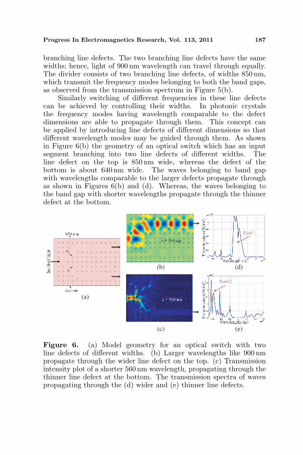
Similarly switching of different frequencies in these line defectscan be achieved by controlling their widths. In photonic crystalsthe frequency modes having wavelength comparable to the defectdimensions are able to propagate through them. This concept canbe applied by introducing line defects of different dimensions so thatdifferent wavelength modes may be guided through them. As shownin Figure 6(b) the geometry of an optical switch which has an inputsegment branching into two line defects of different widths. Theline defect on the top is 850 nm wide, whereas the defect of thebottom is about 640 nm wide. The waves belonging to band gapwith wavelengths comparable to the larger defects propagate throughas shown in Figures 6(b) and (d). Whereas, the waves belonging tothe band gap with shorter wavelengths propagate through the thinnerdefect at the bottom.
(a)
(b)
(c)
(d)
(e)
Figure 6. (a) Model geometry for an optical switch with twoline defects of different widths. (b) Larger wavelengths like 900 nmpropagate through the wider line defect on the top. (c) Transmissionintensity plot of a shorter 560 nm wavelength, propagating through thethinner line defect at the bottom. The transmission spectra of wavespropagating through the (d) wider and (e) thinner line defects.

188 Butt et al.
Figure 7. Simulated electric field intensity of a 950 nm wavepropagating through an optical multiplexer.
2.5. Wavelength Multiplexing
We also demonstrate the application of wavelength multiplexingutilizing the sharp curved photonic crystal waveguides. The frequencymodes within the band gaps can be multiplexed together by branchingline defects in 2D arrays of Si pillars, as shown in Figure 7. Differentfrequency modes can be multiplexed into the common channel throughthe branching line defects. In this fashion numerous efficientlyoperating optical applications can be integrated together at micron-scale using photonic crystals.
3. FABRICATION AND CHARACTERISATION
3.1. Fabrication
The fabrication of 2D arrays of silicon pillars was established by firstusing e-beam lithography to make the dot array pattern (50 nm radius,400 nm lattice constant) on the Si substrate. The pattern was thensputtered with a metal mask (Tungsten). The process of deep reactiveetching (DRIE) was performed for etching the substrate. The array wasthen exposed to the following gases for a second each, in a successionlasting for 5 minutes: C4F8 for protective layering, O2 for removingthe C4F8 residues and SF6 for etching. The final etched substrate wasviewed under the scanning electron microscope and well aligned andpatterned Si pillars were observed as shown in Figure 8.
The Si pillars lattice was pattered with 800 nm wide line defectsproducing waveguides with 90◦ turns. An array of such waveguides

Progress In Electromagnetics Research, Vol. 113, 2011 189
(a) (b)
Figure 8. SEM image of an array of Si pillars with 800 nm wide linedefects. Defects are shaped to produce an array of 90◦ turn waveguidesacting as a multiplexer.
was patterned with their ends opening into a common line defect.The device in this arrangement can be utilized as a photonic crystalmultiplexer for multiplexing the frequency modes within the band gaps.
3.2. Optical Characterisation Results
The optical characterisation of patterned arrays of Si pillars was carriedout. An Ocean Optics 2000 spectrometer was utilized to capture thereflected light from the arrays for the spectral range of almost 450 nmto 1100 nm, with resolution 0.3 nm. Light from a white light sourceused at an incidence angle of around 60◦. The openings of the 90◦waveguides were aligned to the incident light beam. The absorptionspectra were measured for polarizations of light parallel (TE-transverseelectric) and perpendicular (TM-transverse magnetic) to the Si pillars.The light perpendicular to the Si pillars will not be guided throughthe line defects and was mostly reflected, whereas, the incident lightpolarized parallel to the pillars was guided within the line defects, dueto the band gaps and dips were observed in the reflection spectrum.
Measured reflection spectra for both polarizations of light arepresented in Figure 9. In the TM-mode, some strong dips wereobserved in spectrum corresponding to diffracted light. Waves werenot guided through the line defects as the Si pillars do not present aTM-mode photonic band gap. Similar dips were also observed in theTE-mode along with an extra region of increased absorption around730 to 800 nm which corresponds to the frequency modes that areguided through the waveguides. In our simulations, the TE polarizedlight was assumed to be incident at an angle of 90◦ to the Si pillars.However, in experiments an incident angle of near 60◦ was used due towhich the lattice constant offered by the arrays to the incident light

190 Butt et al.
changes and the band gaps shift to smaller wavelengths.
Figure 9. Normalized absorption spectra (TM and TE mode) for anarray of sharp turn waveguides based on Si pillar photonic crystals.The light at an incidence angle of 600 was shined on the photoniccrystal waveguides.
4. METAMATERIAL HIGH PASS FILTERS
The highly dense periodic arrays of thin Si pillars can also beutilized as metamaterials by sputtering them with noble metals. Inthis arrangement the arrays display an artificial dielectric function(different from their own) towards the incident light, due to a lowereffective plasma frequency of order several hundred terahertz. Pendryet al. [8] demonstrated that the electromagnetic response of a metallicarray composed of thin metallic wires, excited by an electric fieldparallel to the wires (TE-mode) is similar to that of a low-densityplasma of very heavy charged particles, with a plasma frequency ωp:
ω2p =
2πc20
a2 ln(a/r)(1)
where c0 is the velocity of light in vacuum, a is the lattice constant ofthe 2D wire array, r is the radius of the wires. This concept can beused for lowering the plasma frequency displayed by the metal coated Sipillar arrays achieving negative dielectric constants for metamaterials.The lowering of the plasma frequency is due to the increase in theeffective electronic mass within the metallic wires due to the inducedcurrent and corresponding magnetic field around them. According to

Progress In Electromagnetics Research, Vol. 113, 2011 191
Eq. (1), the effective plasma frequency strongly depends on the nano-pillar radius and lattice constant. Their values can discretely be chosento engineer Si pillar arrays of a desired plasma frequency. The resultantfrequency dependent permittivity can be calculated using the Drudemodel for metals described as
ε(ω) = 1− ω2p
ω2(2)
The effective permittivity ε(ω) is negative for frequencies less than ωp,therefore no wave propagation will take place inside the metamaterial.Electromagnetic waves propagation only occurs above ωp, due to whichthe structure acts as a nanophotonic high-pass filter [14]. Here wepropose that the structure was realized using metal coated squarelattice array of Si pillars having radius of 50 nm and lattice constant of400 nm. Theoretical calculations of the plasma frequency and reflectioncoefficient of such a nano-scale brush-like array were conducted. For asquare lattice of nano-pillar radius 50 nm and lattice constant 400 nm,the plasma frequency fp = ωp/2π of 207.5 THz with correspondingplasma wavelength of λp = 1.44µm were calculated using Eq. (1).
FEM modeling of an array of Si pillars (with a = 400 nm andr = 50 nm) coated with Aluminum was carried out to confirm thetheoretical results. The geometry of the model was similar to theone previously used however the boundary condition for the Si pillarswas set to the perfect electric conductor for the purpose of modelingmetallic wire arrays. The material properties of the nano-pillars wereset to those of Aluminum in the model. The transmission spectra forboth TE and TM polarization of light were computed using the model,as shown in Figure 10.
(a) (b) (c)
Figure 10. (a) Model geometry of a 2D array of Al pillars, witha = 400 nm and r = 50 nm. The calculated transmission spectra forlight polarized (b) parallel and (c) perpendicular to the pillars.

192 Butt et al.
It can be observed, the TE-mode spectrum of the metallicphotonic crystal presents almost the same alternation of transmissionbands and band gaps (near 300 and 600 nm). Till the wavelength of1µm the TE-mode spectrum is quite similar to the one displayed by theSi nanopillars, previously shown in Figure 1. However, in the regionof larger wavelengths the spectrum exhibits a fundamentally differentaspect. Starting from approximately 1µm, a strong attenuation offeredby the lattice, associated with the plasmon-like photonic band, can beobserved. The cutoff wavelength of approximately 1µm numericallycalculated from the FEM simulation model is close to the valueestimated on the basis of the approximate formula given in Eq. (1)(∼ 1.44µm). The simulation results agree with the metamaterialtheory and after the cut-off frequency no propagation takes placethrough the lattice. The Al pillars array act as a plasmonic high passfilter, towards the incident waves parallel to the pillars. No such cut-offfiltering effect is seen in the TM-mode spectrum (light perpendicularto the pillars), as shown in Figure 10(c). In the TE-mode spectrum(Figure 10(b)) a transmission band is observed just before the cut-offregion, whose centre wavelength (∼ 800 nm) corresponds to λ/2 ∼ a.This is reversed as compared to the spectrum of Si nanopillars inFigure 1, where the same relation corresponded to the wider bandgap of the two. In this transmission window, the metallic pillars basedphotonic crystal behave like a group of Fabry-Perot cavities coupledto one another along the propagation direction [12], leading to thecorresponding transmission peaks.
Through theoretical results we demonstrate that the sputteredperiodic arrays of Si pillars can act as subwavelength wire structuresrequired to establish metamaterials. The fabrication of such arrays
(a) (b) (c)
Figure 11. (a) (b) SEM images of 2D periodic arrays of Si nanopillars(with a = 400 nm and r = 50 nm), which after metal sputtering can actas subwavelength structures in metamaterial filters. (c) The magnifiedimages of the same. The marker represents 400 nm.

Progress In Electromagnetics Research, Vol. 113, 2011 193
was carried out and some SEM images array are shown in Figure 11.Their optical characterization as metamaterial high-pass filter willbe reported later. Accordance to Eq. (1), by decreasing the latticeconstants of these arrays, their plasmon cut-off frequencies can bebrought right in the middle of the optical regime to achieve negativedielectric constant.
5. CONCLUSION
In conclusion, we have presented some interesting applications ofphotonic crystals based on 2D arrays of silicon pillars. The simulatedband gap results were presented for the Si pillars lattice, with a latticeconstant of 400 nm and pillar radius of 50 nm. Finite element modelingwas utilised to demonstrate the efficient performance of photoniccrystals based sharp turn waveguides, optical power dividers, opticalswitches and multiplexers. The fabrication and optical characterisationof Si pillars based photonic crystal waveguides was performed andgood agreement between the two was achieved. We also demonstratedthrough simulation results that metal sputtered Si pillar arrayscan act as subwavelength metallic structures required to establishmetamaterial high-pass filters which display cut-off frequencies in theoptical regime.
REFERENCES
1. Joannopoulos, J. D., S. G. Johnson, R. D. Meade, and J. N. Winn,Photonic Crystals: Molding the Flow of Light, 2nd edition,Princeton University Press, 2008.
2. Poborchii, V. V., T. Tada, and T. Kanayama, “Photonic-band-gapproperties of twodimensional lattices of Si nanopillars,” Journal ofApplied Physics, Vol. 91, 3299–3305, 2002.
3. De Dood, M. J. A., E. Snoeks, A. Moroz, and A. Polman, “Designand optimization of 2D photonic crystal waveguides based onsilicon,” Optical and Quantum Electronics, Vol. 34, 145–159, 2002.
4. Zijlstra, T., E. van der Drift, M. J. A. de Dood, E. Snoeks,and A. Polman, “Fabrication of two-dimensional photonic crystalwaveguides for 1.5µm in silicon by deep anisotropic dry etching,”43rd International Conference on Electron, Ion, and PhotonBeam Technology and Nanofabrication, 2734–2739, Marco Island,Florida, USA, 1999.
5. Sharkawy, A., S. Shi, D. Prather, and R. Soref, “Electro-

194 Butt et al.
optical switching using coupled photonic crystal waveguides,” Opt.Express, Vol. 10, 1048–1059, 2002.
6. Ao, X., L. Liu, L. Wosinski, and S. He, “Polarization beam splitterbased on a twodimensional photonic crystal of pillar type,” AppliedPhysics Letters, Vol. 89, 171115-3, 2006.
7. Sharkawy, A., S. Shi, and D. W. Prather, “Multichannelwavelength division multiplexing with photonic crystals,” Appl.Opt., Vol. 40, 2247–2252, 2001.
8. Pendry, J. B., A. J. Holden, W. J. Stewart, and I. Youngs,“Extremely low frequency plasmons in metallic mesostructures,”Physical Review Letters, Vol. 76, 4773, 1996.
9. Wu, D., N. Fang, C. Sun, X. Zhang, W. J. Padilla, D. N. Basov,D. R. Smith, and S. Schultz, “Terahertz plasmonic high passfilter,” Applied Physics Letters, Vol. 83, 201–203, 2003.
10. Gay-Balmaz, P., C. Maccio, and O. J. F. Martin, “Microwirearrays with plasmonic response at microwave frequencies,” AppliedPhysics Letters, Vol. 81, 2896–2898, 2002.
11. COMSOL, COMSOL Multiphysics User’s Guide & COM-SOL Multiphysics Modeling Guide, 3.3a edition, 2007,http://www.comsol.com.
12. Lourtioz, J. M. and D. Pagnoux, Photonic Crystals: TowardsNanoscale Photonic Devices, Springer, Berlin, 2008.
13. Djavid, M., A. Ghaffari, F. Monifi, and M. S. Abrishamian,“Photonic crystal power dividers using L-shaped bend based onring resonators,” J. Opt. Soc. Am. B, Vol. 25, 1231–1235, 2008.
14. Butt, H., Q. Dai, P. Farah, T. Butler, T. D. Wilkinson,J. J. Baumberg, and G. A. J. Amaratunga, “Metamaterial highpass filter based on periodic wire arrays of multiwalled carbonnanotubes,” Applied Physics Letters, Vol. 97, 163102-3, 2010.