![Spectrum of Applications · [2] These resists are available off the shelf from . Checkerboard arrangement of test patterns fab-ricated in positive-tone resist AZ® 5214 on 4 inch](https://static.fdocuments.in/doc/165x107/5f450499dd680110797088e6/spectrum-of-applications-2-these-resists-are-available-off-the-shelf-from-checkerboard.jpg)
Photomask Making - personal.utdallas.edurar011300/LithographyProcess/Photomask... · process does...
24
Title: Photomask Making Page 1 of 24 Author: Roger Robbins 3/6/2007 Document Number: SP-07-001 The University of Texas at Dallas Photomask Making Roger Robbins 3/6/2007 The University of Texas at Dallas Erik Jonsson School of Engineering
Transcript of Photomask Making - personal.utdallas.edurar011300/LithographyProcess/Photomask... · process does...

Title: Photomask Making Page 1 of 24 Author: Roger Robbins 3/6/2007 Document Number: SP-07-001 The University of Texas at Dallas
Photomask Making Roger Robbins 3/6/2007
The University of Texas at Dallas Erik Jonsson School of Engineering

Title: Photomask Making Page 2 of 24 Author: Roger Robbins 3/6/2007 Document Number: SP-07-001 The University of Texas at Dallas
Photomask Making Roger Robbins 3/6/2007
Table of Contents Photomask Making .......................................................................................................... 2
Table of Contents ........................................................................................................ 2 Photomask Making .......................................................................................................... 3
Purpose ....................................................................................................................... 3 Introduction .................................................................................................................. 3 Mask “Color” ................................................................................................................ 3 Process Description ..................................................................................................... 4
Step 1: Plasma Cleaning .......................................................................................... 4 Step 2: HMDS Application ........................................................................................ 5 Step 3: Resist Application ........................................................................................ 6 Step 4: Pre-Bake ...................................................................................................... 8 Step 5: Lithographic Patterning ................................................................................ 8 Step 6: Post Bake .................................................................................................. 10 Step 7: Develop...................................................................................................... 10 Step 8: Plasma De-scum ........................................................................................ 11 Step 9: Cr Etch ....................................................................................................... 12 Step 10: Resist Removal and Mask Clean ............................................................. 12 Step 11: Final Inspection ........................................................................................ 14 Conclusion ............................................................................................................. 14
Appendix A .................................................................................................................... 15 Appendix B .................................................................................................................... 18

Title: Photomask Making Page 3 of 24 Author: Roger Robbins 3/6/2007 Document Number: SP-07-001 The University of Texas at Dallas
Photomask Making Roger Robbins 3/6/2007
Purpose
This paper describes a starting process for making photomasks with the tools in the UTD Cleanroom. Special needs may dictate variations in this process flow.
Introduction
Photomasks are generally Chrome coated glass lithographic templates designed to optically transfer patterns to wafers or other substrates in order to fabricate planar type devices of all types. Basically the pattern information is created in a drawing package and stored in a database, reformatted and transferred to a lithography tool – laser writer or e-beam writer in our case – then printed in a layer of photoresist coated onto the photomask plate. The imaged pattern is next developed to form a template over the opaque Chrome and then the Chrome is etched away where the resist is clear. After the etch process is complete, the remaining photoresist is removed, the plate cleaned, and then stored for later use in an optical printer. This paper will describe in detail all the fundamental process steps required to fabricate a photomask in the UTD Cleanroom Labs.
Figure 1. Example of standard photomasks: “Clear field” on left, “dark field” on right
Mask “Color”
First, there are some key details to discuss that determine what “color” photomask you will need to make, (Figure 1). Normally, we use “positive” photoresist to make masks. This means that wherever light exposes the photoresist, the developer will wash away the photoresist. This exposed area, then, will expose the Chrome and allow it to be washed away in the acid etch solution, leaving holes in the Chrome through

Title: Photomask Making Page 4 of 24 Author: Roger Robbins 3/6/2007 Document Number: SP-07-001 The University of Texas at Dallas
which light will pass to expose the substrate during the pattern transfer process – (Dark Field mask color).
Following that logic, if the substrate also has positive photoresist, the mask will allow exposure to the substrate in the same pattern as the clear regions on the mask. The development of the substrate resist will produce exposed areas in the same location as the clear areas on the mask. This will allow an etch process to transfer the clear area pattern to an underlying film by etching away the underlying film in the clear area.
This may seem simple to the casual observer, but there is a complication when you consider the common “lift-off” process which will change the “color” of the pattern on the substrate. In the lift-off process, the patterned substrate is first developed and then a film is deposited on top of the patterned resist. The next step strips the resist under the deposited film. This will leave a pattern of deposited film in the areas where the positive photoresist was exposed and leave bare the areas under the unexposed resist that were washed away, taking the deposited film away with the wash.
Then to further complicate a complicated logic, there is negative photoresist which stays put when exposed and washes away in unexposed areas. This negative process does the opposite thing to the above positive resist. The resists can be used either on the mask or the substrate in any order. Thus you must keep exact logical understanding and control of your process in order to make what you want.
Process Description
The following process description will assume that we start with a bare, blank photomask and describe all the steps to fabricate a complete mask. There may be sections that are optional or unnecessary due to the particular situation you have, such as a pre-coated mask that does not need to be coated with photoresist.
Step 1: Plasma Cleaning
Both new and recycled bare photomasks may have a thin invisible layer of organic contamination on the Cr surface. This organic layer will sometimes cause adhesion problems between the Cr and the photoresist later in the process. It also may interfere with the Cr etch process after photomask imaging. However it is easy to remove the contamination with a short, but aggressive Oxygen plasma treatment before starting the photomask process. The current process designed and tested for this purpose is shown in Table 1. It uses the March Asher1 tool, (Figure 2), but fortunately it can be used in any other month of the year as well.
Table I March Asher Cleaning*
Step Parameter Value
1 Vacuum Pressure 230 mTorr
2 Gas O2
3 Gas Flow 31 sccm
4 Time 600 sec
1 Roger Robbins, “March Asher Operation,”
http://www.utdallas.edu/~rar011300/public_html/MarchAsher/MarchAsherOperation.pdf, (7/31/2006)

Title: Photomask Making Page 5 of 24 Author: Roger Robbins 3/6/2007 Document Number: SP-07-001 The University of Texas at Dallas
*Set the photomask Cr side up on the powered electrode plate for RIE conditions.
Figure 2. March Plasma Asher tool: RF power supply at left, Control section in center, and access door to RF plasma chamber on right.
Step 2: HMDS Application
In order to enhance the adhesion of the photoresist to the Cr, we bake the mask in a special oven that applies a molecular monolayer of Hexamethyldisilizane (HMDS), to the surface2. This molecule chemically bonds to the Cr and then bonds to the photoresist so that the photoresist will not allow developers or etch solutions to lift the edges of resist patterns away from the mask. This step is pretty much mandatory for coating a mask prior to exposure. This is a simple process. Basically you open the oven door, insert your mask (riding on a quartz boat), close the door and push the start button. During the oven process, the mask is brought to temperature (120 C), and pressure is automatically cycled between 10 mTorr and 1200 mTorr several times to drive off moisture from the surface of the substrate. The oven fills with HMDS vapor for 5 minutes. This is the application step in which HMDS chemically attaches one end of its molecule to the substrate. The atmosphere in the oven is then cleared of vapor by introducing N2 into the oven and pumping it out again over several cycles. After about 27 minutes, the oven buzzes rather loudly indicating it is done. Reset the buzzer, open the oven door and remove your mask using the forked lifting tool – the mask is hotter than boiling water (120 C). Let it cool. Cooling is important because the temperature uniformity of the mask determines the film thickness uniformity during the spin coating of the resist. To quickly achieve temperature uniformity, set the mask on a cool metal surface like the special ½ in thick Cr plated Stainless steel table normally used to level SU8 photoresist. It will take about 3 – 5 minutes to cool to room temperature.
2 Daggett, Joe, Villareal, Sam, and Robbins, Roger, “UT Dallas IC Fabrication Laboratory HMDS
Process Setup,” http://www.utdallas.edu/research/cleanroom/documents/HMDS_Process.pdf, (2/21/2003).

Title: Photomask Making Page 6 of 24 Author: Roger Robbins 3/6/2007 Document Number: SP-07-001 The University of Texas at Dallas
Figure 3. HMDS Oven showing logbook, mask, quartz holder with extractable handle and open door. The start button is the black button in the upper center of the control box. The red button is the reset and buzzer silencer.
Step 3: Resist Application
After the blank photomask is prepared, the next step is to apply the photoresist. This is done on the CEE spinner3 manually, (Figure 4). We use two photoresists for photomasks in our lab: S1813, and AZ1518. (See Appendix A and B for resist spec sheets). Normally, the AZ1518 is pre-applied by the photomask vendor, and we don’t have to worry about applying that resist. But if we are coating a blank one, we normally use the S1813 or a new, faster resist AZ TFP650.
3 Robbins, Roger “CEE Spin Coater/Hotplate Operation,”
http://www.utdallas.edu/research/cleanroom/documents/CEEcoater.pdf, (10/7/2004).

Title: Photomask Making Page 7 of 24 Author: Roger Robbins 3/6/2007 Document Number: SP-07-001 The University of Texas at Dallas
Figure 4. Manual application of S1813 photoresist to a blank photomask in the CEE spinner. You must be trained on this tool before using. The design of the CEE spinner requires that you learn how to program the spin cycle. This is described in detail in reference #3, but verbal instruction with demonstration is required. The parameters of a nominal coating program are listed in Table 2. These parameters are regularly changed by users, so you must first check the installed values and put in your own values before coating.
Table 2 CEE Spinner Parameters for Mask Photoresist Coating
Step Parameter Value
1 Dispense 0
2 Spin Speed #1 500 rpm
3 Acceleration 500 rpm/sec
4 Spin Time Duration #1 2 sec
5 Spin Speed #2 4000 rpm
6 Acceleration 4000 rpm/sec
7 Spin Time Duration #2 60 sec
The resist is dispensed from a plastic pipette by sucking up just the right amount of liquid photoresist and dispensing it onto the center of the wafer and then closing the lid and starting the CEE spin cycle. For a 5 inch square photomask, the amount of photoresist is about 2 ml. The first spin cycle quickly spreads the resist without throwing it off the mask, and the second spin cycle stretches the resist film into a highly uniform thin film at the desired thickness based on a spin-speed curve from the manufacturer. For a photomask, you would typically want about 6,000 – 10,000Ǻ of thickness.

Title: Photomask Making Page 8 of 24 Author: Roger Robbins 3/6/2007 Document Number: SP-07-001 The University of Texas at Dallas
Step 4: Pre-Bake
After the resist is coated it still contains a considerable amount of solvent that needs to be driven out via a moderately high temperature bake. This is usually done on the integral CEE spinner hotplate shown in Figure 5. This step is called “pre-bake” because it happens before exposure.
Figure 5. CEE spinner hotplate with mask baking under exhaust lid. The CEE spinner has a special programmable hotplate with an integral hinged lid with fume exhaust capabilities. This lid captures the solvent vapors emanating from the hot photoresist, and ports them away from your nose so you won’t come down with central nervous system problems. Table 3 lists the baking parameters for S1813. Temperature and time are important here and vary with the photoresist type.
Table 3 Bake Parameters for S1813 Photoresist
Step Parameter Value
1 Temperature 115 C
2 Bake Time 90 sec
Step 5: Lithographic Patterning
Lithography is a complex process and will not be described here in detail. In the UTD clean room there is one method for making photomasks – the Heidelberg

Title: Photomask Making Page 9 of 24 Author: Roger Robbins 3/6/2007 Document Number: SP-07-001 The University of Texas at Dallas
Instruments “DWL-66” laser mask writer. The principle steps involved in making a mask are listed below.
Create a device design.
Lay out the mask geometries using a drawing package such as AutoCad.
Convert the drawing data into a form familiar to the DWL-66 computer (.cif), using a special conversion software and special separate computer. Note: You should write a label on each mask you make to avoid using the wrong mask during your device fabrication.
Send the converted data to the DWL-66 computer.
Reserve time on the DWL-66 laser writer
Sign the Logbook
Load the resist coated photomask blank onto the laser writer stage.
Set up the layout on the DWL-66 computer.
Setup the job on the DWL-66 computer.
Focus the DWL-66.
Find the center of the photomask blank.
Start the Job.
Wait a long, long time before the mask is complete (many hours).
Remove the mask from the DWL-66.
Basically, the exposure step modifies the chemistry of the photoresist so that the exposed portion either dissolves in the developer and washes away - (Positive resist), or solidifies and remains on the mask while all the unexposed resist washes away in the developer - (Negative resist). The two photo resists listed in this document are positive resists which wash away after exposure.
There are a lot of pitfalls involved with the stream of actions listed above – you must follow them exactly – deviations may cause computer confusion crashes. The lithography step will require extensive training and practice along with recurrent help – ask if you are uncertain. Use the available instruction sheets for detailed guidance so you won’t forget anything. Let us assume here that the lithography exposure goes well. Figure 6 shows the illustrious DWL-66 mask writer.
Figure 6. DWL-66 Laser Mask Writer

Title: Photomask Making Page 10 of 24 Author: Roger Robbins 3/6/2007 Document Number: SP-07-001 The University of Texas at Dallas
Step 6: Post Bake
Some resists require a short bake after exposure to “activate” the exposure. The two photomask resists, S1813 and AZ1518 do not, so we just skip right by this step in this document.
Step 7: Develop
After exposure, the resist needs development to show the pattern. Each photoresist has its own developer and we have automatic programs set up in the CPK spin developer tools to develop your mask or wafer, (Figure 7). For optical resists, the developer chemical is basically a solution of Tetra Methyl Ammonium Hydroxide (TMAH). The rinse cycle utilizes de-ionized water.
Figure 7. Photo of the CPK Spin Develop/Etch tool. The process fluids are forced through the spray nozzles via pressurized source tanks (black tanks with green bolt handles in lower drawers). Note the “POLOS” controller panel at the top left of the overhead panel – this is where the tool is programmed and where process progress is displayed. Also note that if a light goes on above one of the switches at the top right, the fluid is low in that particular pressure canister. It will complete the current process even if the light goes on during process. The steps involved in developing the mask in the CPK acid/base developer tool are as follows:
Sign the LOGBOOK
Insure that the machine is on – press the green start button on the overhead panel if needed.
When the display asks for help, follow the directions on screen and press the “other” button – (the blank pad between the “MODE” and “UP arrow”).
If required, exchange the substrate holder for the appropriate sized mask holder. This involves turning off the “VACUUM” on the controller panel and lifting the chuck off the spindle, then replacing it with the appropriate mask holder. Note that the fit between holder and spindle is tight and requires that the two posts on the spindle fit into the receiver holes on the
Title: Photomask Making Page 11 of 24 Author: Roger Robbins 3/6/2007 Document Number: SP-07-001 The University of Texas at Dallas
bottom of the chuck assembly. Place the chuck over the spindle and slide it around until the two posts slip into the receiver holes and the chuck base seats against the o-ring in the spindle.
Turn on the vacuum by pressing the “VAC” button on the overhead panel controller. Check to see that the chuck is properly seated and will not wobble excessively during the rotation.
Place the mask securely inside the corner posts on the substrate holder.
Close the lid.
Select the proper program number from the list of programs posted just under the controller on the overhead panel. Enter this program number by pressing the “PROGRAM” button, entering the appropriate number, (2 for S1813), then pressing the “ENTER” button.
To start the develop program, press the I/O button at the lower left of the overhead display.
The develop program has a multitude of steps and comes to a complete stop several times to “puddle-develop” in order to save developer fluid.
Allow the program to complete and then press “VAC” to open the lid and remove your developed mask. NOTE: These lids are notorious for dripping fluid droplets on perfectly good masks – be very gentle in lifting the lid.
Close the lid and remove your mask.
Step 8: Plasma De-scum
After development, have a look at your pattern under a microscope. Look at it for a long time to check the pattern and quality of develop. Look for things like scalloped resist edges, lifted resist, pinholes, under or over development, particles, and other things that look like they could damage the image. If a severe fault is found, do not go on to the next step. Stop and recycle the mask. The resist can be stripped off and new resist applied at this point, saving cost and material. If the inspection goes well, you need to prepare for the Cr etch. The first thing to do here is to insure that all of the pattern will etch in the etch time allowed. This can be helped if you do a very light O2 “de-scum” etch in the March Asher. The “de-scum” etch parameters are listed in Table 4.
Table 4 March Etcher “Descum” Parameters
Parameter Value
1 Gas O2
2 Flow of gas 31
3 RF Power 50 Watts
4 Etch Time 10 sec
The effect of this light etch is to clean out the bottom of the developed features in the resist. This insures that there are no areas covered with a very thin film of resist left by the developer. If all is clean, the etch process will be uniform and complete all at once.

Title: Photomask Making Page 12 of 24 Author: Roger Robbins 3/6/2007 Document Number: SP-07-001 The University of Texas at Dallas
Step 9: Cr Etch
After the short plasma “de-scum,” it is time to do the Cr etch. This etch can be accomplished on the CPK developer/etcher that developed the mask in the first place. Just select the Cr etch program and set the mask firmly into the corner post nests. The actual operation is very similar to the CPK develop program in Step 7, and the steps are outlined below.
Sign the LOGBOOK
Insure that the machine is on – press the green start button on the overhead panel if necessary.
When the display asks for help, follow the directions on screen and press the “other” button – (the blank pad between the “MODE” and “UP arrow”).
If required, exchange the substrate holder for the appropriate sized mask holder. This involves turning off the “VACUUM” on the controller panel and lifting the chuck off the spindle, then replacing it with the appropriate mask holder. Note that the fit between holder and spindle is tight and requires that the two posts on the spindle fit into the receiver holes on the bottom of the chuck assembly. Place the chuck over the spindle and slide it around until the two posts slip into the receiver holes and the chuck base seats against the o-ring in the spindle.
Turn on the vacuum by pressing the “VAC” button on the overhead panel controller. Check to see that the chuck is properly seated and will not wobble excessively during the rotation.
Place the mask securely inside the corner posts on the substrate holder.
Close the lid.
Select the proper program number from the list of programs posted just under the controller on the overhead panel. Enter this program number by pressing the “PROGRAM” button, entering the appropriate number, (4 for Cr Etch), and hitting the “ENTER” button.
To start the etch program, press the I/O button at the lower left of the overhead display.
The etch program has a multitude of steps and comes to a complete stop several times to “Puddle” develop in order to save etch fluid.
Allow the program to complete and then press “VAC” to open the lid and remove your etched mask. NOTE: These lids are notorious for dripping droplets on perfectly good masks, so be very gentle in lifting the lid.
Close the lid.
Step 10: Resist Removal and Mask Clean
After inspecting the etched pattern under a microscope, it is time to remove the photoresist from the mask. This is done to avoid polymer-to-polymer contact at the contact print step between the old resist on the mask and the new coat of resist on a wafer. Polymer contact generates high friction and the resist on the wafer could be torn by sliding the wafer around during alignment. This resist removal can usually be done in the solvent CPK spinner. This tool is very similar to the CPK Chrome etch spinner – identical control and user interface, so

Title: Photomask Making Page 13 of 24 Author: Roger Robbins 3/6/2007 Document Number: SP-07-001 The University of Texas at Dallas
the instructions are almost identical to the previous section – simply select the Acetone Strip program and run your mask. This process uses puddles of Acetone to dissolve the photoresist remaining on the photomask and then spins it off and finally rinses the mask with Isopropyl Alcohol. To assure that the photoresist film is chemically removed, you can also send the mask through the March Asher using the same procedure as described in Step 1: “Plasma Cleaning.”
Mask Cleaning
As a final cleanup to remove remnants from the CPK process, particularly from the back side, you can clean the mask in the UltraTech Mask Washer. Use program “0” for a simple high pressure DI water wash of both sides. This tool is pictured in Figure 8 with its control panel. Note that the big rotor has to be balanced before starting the wash. When you load your mask onto the spin wheel, another mask of the exact mass as yours has to be loaded opposite to yours or the resulting momentum vibration during the spin cycle will cause the tool to stop to protect itself and your mask from disaster. Make sure the balancing mask is the same mass as your mask – compare the thickness! The Door to the chamber opens by sliding downwards after you release the latch with the black button at the lower left of the control panel (below and left of the “Big Red emergency OFF” button).
To select the program to run, press “Go To Program,” then “0,” and then “Enter” to access the water-only wash program “0.” This will load the “0” program and indicate it by placing a “0” in the “Prog” box in the upper right of the keypad area. To start the program, press the “Off/On Start” button in the upper left of the instruction keypad.
Figure 8. UltraTech Mask Washer.

Title: Photomask Making Page 14 of 24 Author: Roger Robbins 3/6/2007 Document Number: SP-07-001 The University of Texas at Dallas
Step 11: Final Inspection
The last step should be a thorough inspection of the etched pattern. It is better to find errors and poor quality at this stage than after a bad pattern that can potentially ruin a multi-level substrate.
Conclusion
This document has briefly illustrated the Masking making lithography trail through the UTD Clean Room Labs. Once the mask is made, a new trail is followed to transfer the mask pattern to a substrate to build a device. That trail is multivariate and depends on the device being fabricated. Usually, instruction for that portion of the trail is obtained from your research group or directly from literature. Cleanroom staff can help with additional advice if necessary. Take care and be SAFE!

Title: Photomask Making Page 15 of 24 Author: Roger Robbins 3/6/2007 Document Number: SP-07-001 The University of Texas at Dallas
Appendix A S1813 Photoresist Spec Sheet
Rather than clutter up this document with an appendix of many pages, please find the data on the web. The spec sheet for S1813 photoresist can be found on the web at the following address: http://cmi.epfl.ch/materials/Data_S1800.pdf Well, I suppose I should include the spin speed curves and the dose characteristic since I had to include the data sheet for the other resist.

Title: Photomask Making Page 16 of 24 Author: Roger Robbins 3/6/2007 Document Number: SP-07-001 The University of Texas at Dallas

Title: Photomask Making Page 17 of 24 Author: Roger Robbins 3/6/2007 Document Number: SP-07-001 The University of Texas at Dallas

Title: Photomask Making Page 18 of 24 Author: Roger Robbins 3/6/2007 Document Number: SP-07-001 The University of Texas at Dallas
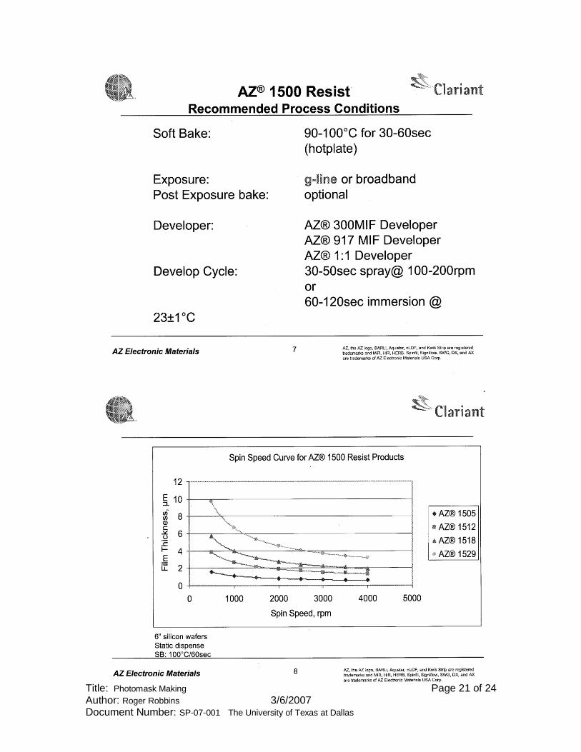
Appendix B AZ1518 Photoresist Spec Sheet
It seems that the manufacturer of AZ1518 does not post its data sheets on the internet. Consequently, I will clutter up this document with a copied version of their data sheet.

Title: Photomask Making Page 19 of 24 Author: Roger Robbins 3/6/2007 Document Number: SP-07-001 The University of Texas at Dallas

Title: Photomask Making Page 20 of 24 Author: Roger Robbins 3/6/2007 Document Number: SP-07-001 The University of Texas at Dallas
Title: Photomask Making Page 21 of 24 Author: Roger Robbins 3/6/2007 Document Number: SP-07-001 The University of Texas at Dallas

Title: Photomask Making Page 22 of 24 Author: Roger Robbins 3/6/2007 Document Number: SP-07-001 The University of Texas at Dallas

Title: Photomask Making Page 23 of 24 Author: Roger Robbins 3/6/2007 Document Number: SP-07-001 The University of Texas at Dallas

Title: Photomask Making Page 24 of 24 Author: Roger Robbins 3/6/2007 Document Number: SP-07-001 The University of Texas at Dallas