Immersion Lithography: Photomask and Wafer-Level Materials · 2016-12-27 · ANRV380-MR39-05 ARI 27...
36
Immersion Lithography: Photomask and Wafer-Level Materials Roger H. French and Hoang V. Tran DuPont Co. Central Research, E400-5207 Experimental Station, Wilmington, DE 19880-0400; email: [email protected] Annu. Rev. Mater. Res. 2009. 39:93–126 First published online as a Review in Advance on March 3, 2009 The Annual Review of Materials Research is online at matsci.annualreviews.org This article’s doi: 10.1146/annurev-matsci-082908-145350 Copyright c 2009 by Annual Reviews. All rights reserved 1531-7331/09/0804-0093$20.00 Key Words photoresist, pellicle, high-index fluid, phase shift, double patterning Abstract Optical immersion lithography utilizes liquids with refractive indices >1 (the index of air) below the last lens element to enhance numerical aper- ture and resolution, enabling sub-40-nm feature patterning. This shift from conventional dry optical lithography introduces numerous challenges re- quiring innovations in materials at all imaging stack levels. In this article, we highlight the recent materials advances in photomasks, immersion fluids, topcoats, and photoresists. Some of the challenges encountered include the fluids’ and photomask materials’ UV durability, the high-index liquids’ com- patibility with topcoats and photoresists, and overall immersion imaging and defectivity performance. In addition, we include a section on novel materi- als and methods for double-patterning lithography—a technique that may further extend immersion technology by effectively doubling a less dense pattern’s line density. 93 Annu. Rev. Mater. Res. 2009.39:93-126. Downloaded from arjournals.annualreviews.org by Dr. Roger French on 07/14/09. For personal use only.
Transcript of Immersion Lithography: Photomask and Wafer-Level Materials · 2016-12-27 · ANRV380-MR39-05 ARI 27...

ANRV380-MR39-05 ARI 27 May 2009 14:25
Immersion Lithography:Photomask andWafer-Level MaterialsRoger H. French and Hoang V. TranDuPont Co. Central Research, E400-5207 Experimental Station, Wilmington, DE 19880-0400;email: [email protected]
Annu. Rev. Mater. Res. 2009. 39:93–126
First published online as a Review in Advance onMarch 3, 2009
The Annual Review of Materials Research is online atmatsci.annualreviews.org
This article’s doi:10.1146/annurev-matsci-082908-145350
Copyright c© 2009 by Annual Reviews.All rights reserved
1531-7331/09/0804-0093$20.00
Key Words
photoresist, pellicle, high-index fluid, phase shift, double patterning
AbstractOptical immersion lithography utilizes liquids with refractive indices >1(the index of air) below the last lens element to enhance numerical aper-ture and resolution, enabling sub-40-nm feature patterning. This shift fromconventional dry optical lithography introduces numerous challenges re-quiring innovations in materials at all imaging stack levels. In this article,we highlight the recent materials advances in photomasks, immersion fluids,topcoats, and photoresists. Some of the challenges encountered include thefluids’ and photomask materials’ UV durability, the high-index liquids’ com-patibility with topcoats and photoresists, and overall immersion imaging anddefectivity performance. In addition, we include a section on novel materi-als and methods for double-patterning lithography—a technique that mayfurther extend immersion technology by effectively doubling a less densepattern’s line density.
93
Ann
u. R
ev. M
ater
. Res
. 200
9.39
:93-
126.
Dow
nloa
ded
from
arj
ourn
als.
annu
alre
view
s.or
gby
Dr.
Rog
er F
renc
h on
07/
14/0
9. F
or p
erso
nal u
se o
nly.

ANRV380-MR39-05 ARI 27 May 2009 14:25
Photoresist:light-sensitive polymerformulations used todefine structuralfeatures in integrated-circuit processing
Deep UV light(DUV): normallyreferring to the248-nm peak intensityof the KrF excimerlaser
1. INTRODUCTION
In semiconductor fabrication optical lithography, the main materials development has traditionallybeen polymeric photoresists, which changed substantially each time the lithographic wavelengthdecreased: from 436 nm (G-line) to 365 nm (I-line) to 248 nm [deep UV light (DUV)] to thecurrent 193 nm. For example, the shift to DUV (KrF excimer laser) coincided with the intro-duction of chemically amplified resists. Currently, the transition to 193 nm (ArF excimer laser),along with a failed transition to 157 nm (F2 excimer laser), has expanded greatly the number andtype of materials needed above and below the projection lens in lithographic scanners (Figure 1).These new materials include both photomask materials (Figure 2) as well as new types of wafer-level materials, such as immersion fluids (Figure 3). These new materials—photomasks, pellicles,
Projectionlens
Photomask
Illuminator
Alignment andimaging stages
Figure 1ASML TwinScan XT:1950i scanner showing the illuminator, the reticle (photomask) and reticle handler, theprojection lens, and the wafer stages. The illuminator, which prepares the ArF excimer laser light, is on theright. The photomask on the left side, above the large cylindrical projection lens, and the dual-wafer stagesbelow the projection lens are shown, with the left wafer stage undergoing alignment procedures. Meanwhile,the right wafer stage, under the last lens element of the projection lens, is exposing the fields of the waferunder water immersion conditions. The numerical aperture of this water immersion stepper is 1.35, and theproductivity is >140 wafers per hour imaged. Image reprinted courtesy of ASML Inc., Veldhoven, TheNetherlands.
94 French · Tran
Ann
u. R
ev. M
ater
. Res
. 200
9.39
:93-
126.
Dow
nloa
ded
from
arj
ourn
als.
annu
alre
view
s.or
gby
Dr.
Rog
er F
renc
h on
07/
14/0
9. F
or p
erso
nal u
se o
nly.

ANRV380-MR39-05 ARI 27 May 2009 14:25
Figure 2Two photomasks with pellicles. The upper mask is a conventional binary-intensity mask, with the maskpattern and the pellicle on the lower surface of the 6 × 6 inch ultrahigh-purity fused silica photomasksubstrate. The lower mask is a negative-tone phase shift mask, and the mask pattern and the pellicle are onthe upper surface of the substrate. Photograph reprinted courtesy of Toppan Photomasks Inc., Round Rock,Texas.
Scanner (or stepper):the processing toolused in the mainlithographic imagingstep in advancedintegrated-circuitprocessing
photoresists, bottom antireflection coatings (BARCs), and topcoats—coupled with the introduc-tion of immersion lithography, have enabled much larger optical scanner numerical aperture (NA)lenses (up to 1.35 NA with water as the immersion fluid), enabling 45-nm half-pitch feature print-ing using 193-nm light. Before the 1993 lithographic materials review published in this journal’spredecessor (1), the focus was on photoresists and advances in chemically amplified resists. Today,immersion lithography’s development has led to the introduction of immersion fluids, topcoats,and novel photoresist components to manage fluid-resist interactions and to reduce any possiblelens contamination. Immersion lithography materials have become a broad, diverse, and complexfamily developed to help the industry’s advance to 32-nm half-pitch feature sizes. At the same
www.annualreviews.org • Immersion Lithography 95
Ann
u. R
ev. M
ater
. Res
. 200
9.39
:93-
126.
Dow
nloa
ded
from
arj
ourn
als.
annu
alre
view
s.or
gby
Dr.
Rog
er F
renc
h on
07/
14/0
9. F
or p
erso
nal u
se o
nly.

ANRV380-MR39-05 ARI 27 May 2009 14:25
nglass
nfluid
ntopcoat
nresistθ
resist
Figure 3Immersion lithography imaging stack showing the projection lens optics, including the last lens elementcontacting the immersion fluid, and a topcoat layer on top of the photoresist layer. Adapted from Reference34, with permission from SPIE.
Photomask:lithographicphotomasks aretypically transparentfused silica blankscovered with a patterndefined with a chromemetal absorbing film
Pellicle: a thintransparent filmstretched over a framethat is glued over oneside of the photomaskto serve as a dustprotector
Bottomantireflection coating(BARC): an inorganicor organic thin filmused between thephotoresist and thesemiconductor wafer,used to control thereflectance of lightfrom the wafer back upinto the photoresistlayer
Topcoat: a polymercoating used above thephotoresist to reduceinteractions between aphotoresist and animmersion fluid
time, the possible uses of second-generation immersion fluids, double or triple patterning, andnovel resist processes indicate that the need for new and optimized materials will not be reducedin the future.
1.1. Microfabrication
Microfabrication—first developed for integrated circuit processing—has relied on photolithogra-phy as a critical pattern transfer process. From the first transistor in 1947 and the first integratedcircuit (IC) or semiconductor device in 1959, the basic microfabrication process steps have beendeposition, etch, implant, and patterning (2). Patterning has included photolithography in eithercontact or proximity modes (where the photomask and the IC have the same 1:1 feature size ratio)as well as the now dominant projection mode (where there is a 4:1 or 5:1 optical reduction ofthe mask features to the IC feature sizes). Rayleigh’s equations (3) provide a simple relationshipbetween the stepper/scanner optical parameters—such as the lithographic wavelength (λ), the lensnumerical aperture [NA = sin(θ) where θ is the half cone angle of focus], the imaging medium’srefractive index (1 for air and higher for immersion fluids)—and the feature size (FS) and depthof focus (DOF) that can be achieved. These equations also include a process latitude factor (k),where k1 corresponds to the FS equation (Equation 1) and k2 the DOF equation (Equation 2),and where we define the scanner’s NA as NASystem = NADry nImaging medium, where n is the index ofrefraction of the immersion fluid determined at the lithographic wavelength λ (4). k depends onthe overall process capability, and thereby includes the beneficial imaging contributions of phaseshift masks, photoresists with improved imaging, and development characteristics along with step-per settings, such as dipole or quadrapole illuminations, which are beyond the simple NA and λ
characteristics of the scanner. Microfabrication’s progression down this Moore’s law (5–7) featuresize path for complementary metal oxide semiconductor (CMOS) devices has been enabled bytechnological advances in optics, usable lithographic wavelengths, and most recently, immersionfluids to allow projection lens NAs above 1. We summarize this lithography evolution in Table 1,where we include half pitch feature sizes and the corresponding Rayleigh’s equation parameters,
96 French · Tran
Ann
u. R
ev. M
ater
. Res
. 200
9.39
:93-
126.
Dow
nloa
ded
from
arj
ourn
als.
annu
alre
view
s.or
gby
Dr.
Rog
er F
renc
h on
07/
14/0
9. F
or p
erso
nal u
se o
nly.

ANRV380-MR39-05 ARI 27 May 2009 14:25
Integrated circuit(IC): also referred toinformally as acomputer chip
Depth of focus(DOF): a definingparameter in aphotoresist’s imagingperformance; thedepth range of thewafer over which thefeature sizes are withinspecification. Typicallydefined as the waferplane height variationthat leads to a+/−10% variation ofthe critical dimension(CD), or width, of thelithographicallyprinted feature
Moore’s law: anempirical relationshipfirst stated by Intelcofounder GordonMoore in 1965, i.e.,the number oftransistors in anintegrated circuitdoubles (atapproximatelyconstant cost) everytwo years
Extreme UV light(EUV): theplasma-generated13.5-nm radiationbeing studied foradvancedintegrated-circuitphotolithographicapplications
with the associated lithography tool characteristics and lithography materials choices. This canserve as a roadmap to the materials science discussed in this review. During this lithographyevolution, microfabrication and optical lithography have also expanded beyond semiconductorICs to include flat-panel displays, microelectronic machines and devices, photovoltaic solar cells,and other applications, further driving the motivation to improve optical lithography’s capabilities.In addition, as IC feature sizes have decreased, physical limits on materials and processes have ledto new materials and device architectures, such as the IC interconnect conversion from aluminumto dual damascene copper metallization, the transition from silica interconnect dielectrics andgate dielectrics, and new gate architectures [such as the strained gate or 3-D gate geometriesof FinFET devices (8)]. Both microfabrication’s widening applications and the incorporation ofnew materials, process technologies, and architectures into IC fabrication demonstrate the broadplatform that microfabrication represents for materials research, as well as the large technologybase it provides to the semiconductor, display, and photovoltaic industries.
FS = k1λ/NA, 1.
DOF ≈ k2λ/NA2, 2.
1.2. Nanofabrication and Soft Lithography
During photolithographic patterning’s ongoing development for microfabrication, there havebeen parallel efforts on novel new technologies to displace photolithography. For example, X-rayproximity lithography, ion beam and e-beam projection, and e-beam direct-write lithography haveall been the focus of large and substantial research and development efforts. However, other thanthe critical role that e-beam direct-write has played in photomask patterning for optical lithog-raphy, none of these technologies has succeeded in displacing optical projection lithography (9).E-beam direct-write has been pursued in both single e-beam and massively parallel multibeammodes—the latter to improve the technology’s pattern transfer rate and to compete with pro-jection optical lithography’s productivity. Instead of hard X-ray proximity lithography, there hasbeen substantial research in the past 15 years on soft X-ray projection lithography [now calledextreme UV (EUV) lithography] using 13.5-nm light and multilayer reflective mirror optics; thistechnology is now considered a next-generation lithography to replace optical projection lithog-raphy. For more on EUV lithography materials issues, see the article in this volume by Sewell &Mulkens (10).
There has been much recent work on soft lithography: imprint lithography whereby eitherstamping with an elastomeric patterned mask, or hard mask contacting either photo or thermallypolymerizable materials, allows direct pattern transfer (11). This nanoimprint technology, dis-cussed in an article in this volume by Willson and coauthors (12), can make very fine featuresizes. There is also recent work on dip pen lithography, or scanning probe lithography, which(like e-beam direct write) utilizes an atomic force microscope tip to directly write the patterneither with a single probe or with a probe array (13). In addition, there is much research on bothself-assembly of small molecules and oligomers, as well as templated growth. Templated growthinvolves the exploitation of small structural features (which may be introduced by patterning) toconstruct complex functional materials or devices that use materials growth on the template. Rossprovides an example in discussing patterned magnetic media (14).
1.3. The Ongoing Evolution of Photolithography
Projection optical lithography (or photolithography) has continued meeting semiconductor de-vice makers’ patterning needs since the industry’s inception, with photolithographic advances
www.annualreviews.org • Immersion Lithography 97
Ann
u. R
ev. M
ater
. Res
. 200
9.39
:93-
126.
Dow
nloa
ded
from
arj
ourn
als.
annu
alre
view
s.or
gby
Dr.
Rog
er F
renc
h on
07/
14/0
9. F
or p
erso
nal u
se o
nly.

ANRV380-MR39-05 ARI 27 May 2009 14:25
Photoacid generator(PAG): a photoresistformulationcomponent thatgenerates a proton onexposure to light at thelithographicwavelength
providing a large part of the feature size/density improvements that contribute to Moore’s lawadvances (15). The main drivers of these advances have been the shifts to shorter lithographywavelengths, improvements in stepper or scanner illuminators and projection lens optics, andphotoresist improvements. The movement over the years to shorter lithography wavelengths hasprogressed from the mercury emission lines of G-line (436 nm) all the way to 193 nm (ArF ex-cimer) and most recently and unsuccessfully, 157 nm (F2 excimer). In 1976, G-line light was usedwith contact or proximity lithography (with a mask aligner still found to this day) and diazonaph-thoquinone/novolak resists to produce 5–6-μm feature sizes (16). By 1987, the state of the art hadapproached 1-μm feature sizes using I-line wavelengths, as well as projection lithography witha 4 × reduction between the mask and the pattern produced in the photoresist (17). The nextstep was to enter the submicrometer lithography regime, which was considered a great opticalprojection lithography challenge and was not certain to be achieved. Submicrometer lithogra-phy was enabled by introducing 248 nm as the lithographic wavelength—initially from mercurylines and then from KrF excimer lasers—coupled with the development of chemically amplifiedphotoresists based on polyhydroxystyrene (PHOST). In these photoresists, a photoacid genera-tor (PAG) (excited by the 248-nm light) would photocatalytically decompose the positive pho-toresist, leading to a large number of deprotection events from a single absorbed photon. Thisadvance dramatically improved 248-nm lithography’s sensitivity and also led to unprecedentedphotolithographic pattern formation control such that by 1993 feature sizes of 0.5 μm wereproduced in commercial ICs. Subwavelength lithography was enabled not only by improved pho-toresist processes, but also by the introduction of phase shift photomasks, which took advantageof phase of the light: Instead of intensity based on photoresist exposure [as with a traditional
98 French · Tran
Ann
u. R
ev. M
ater
. Res
. 200
9.39
:93-
126.
Dow
nloa
ded
from
arj
ourn
als.
annu
alre
view
s.or
gby
Dr.
Rog
er F
renc
h on
07/
14/0
9. F
or p
erso
nal u
se o
nly.

ANRV380-MR39-05 ARI 27 May 2009 14:25
binary-intensity mask (BIM)], adding phase contrast to the latent image formation enhancesthe ability to produce subwavelength features. Attenuating phase shift masks (APSMs) are dis-cussed below; for I-line lithography, they enabled 250-nm feature printing using 365-nm light in1994.
Since the last Annual Review of Materials Research (and predecessor journal) articles on lithog-raphy (1, 16–18), there have been advances in our quantitative understanding of the physics andchemistry of photoresist imaging and etching, giving new insights into the polymer interfaces(18) that result from photolithography. For example, the study of both line edge roughness (LER)or line width roughness (19) has become critical; LER can now account for a major portion ofline width variation. The line roughness fundamentals obtained from the imaging process’ pho-tochemistry have been extensively examined by new experimental methods characterizing thereaction-diffusion front (20) in chemically amplified resists using infrared spectroscopy (21) andX-ray absorption fine structure (22). These new approaches have also played an important role inimmersion lithography by elucidating the role of the size of the PAGs in imaging (23). In addition,the photoresists’ robustness under etch conditions and the resulting surface roughness levels havebecome a focus of study (24). These experimental advances have also been coupled with a moredetailed understanding of the photoimaging process, resulting in improved quantitative metricsfor comparing photoresists’ performance (25).
It appears that 193-nm photolithography could be the last optical lithography generation,extended by immersion lithography versus making another wavelength change (26). Researchon 193-nm optical lithography began in the early 1990s and immediately had challenges:PHOST resists were too optically absorbing to 193-nm light; moreover, SiO2 glass exhibiteddensification under 193-nm irradiation, producing damaging aberrations in the projection optics.
www.annualreviews.org • Immersion Lithography 99
Ann
u. R
ev. M
ater
. Res
. 200
9.39
:93-
126.
Dow
nloa
ded
from
arj
ourn
als.
annu
alre
view
s.or
gby
Dr.
Rog
er F
renc
h on
07/
14/0
9. F
or p
erso
nal u
se o
nly.

ANRV380-MR39-05 ARI 27 May 2009 14:25
These problems were addressed by new photoresist compositions, with the methacrylate resistsbeing most commonly used today for 193-nm resists, and by tighter control of the glass composi-tion and stoichiometry, thus removing the densification-induced optical aberrations. With theseimprovements, 193-nm lithography was introduced in commercial production in the early 2000sand is now the dominant photolithography for leading-edge production.
Once the research and development pipeline for 193-nm lithography was under way, 157 nmfrom F2 excimer lasers was proposed in 1997 as the next lithography wavelength, with research anddevelopment starting in earnest in 1999 (27). For 157-nm lithography, the number of challengeswas even larger: SiO2 glass, photoresist polymers, and pellicle polymers are not transparent at157 nm (pellicles are used as in situ dust covers on photomask reticles). Therefore, a suite of newmaterials, with CaF2 the designated lens material and fluorine-doped SiO2 the glass for photomasksubstrates, and much work were needed to develop photoresist and pellicle polymers. Considerableprogress in materials research was achieved on 157-nm photolithography. However, in the end,157-nm lithography failed in 2003 owing to an inability to produce CaF2 of the required opticalquality (acceptable levels of stray light and flare arising from scattering in the material) for aprojection lens.
In 2002, immersion lithography (28) was proposed. For the first time in optical lithogra-phy’s history, the transition was not from wavelength to wavelength. Instead, the transition in-volved changing the imaging medium between the lens and the photoresist-coated wafer, from air(193-nm refractive index = 1) to a liquid such as water (193-nm refractive index = 1.436). Withthe imaging being done under water, the effective wavelength of a 193-nm ArF excimer laser isreduced to 193.4/1.436 = 134.7 nm. Thus, the imaging wavelength in essence shrinks while stillusing an established light source. This advance avoids extensive CaF2 crystal use for the projectionlens because the reduction lens remains in air, and only below the last lens element is imagingdone in the immersion fluid. The optical lithography roadmap now appears to have its terminallithography wavelength, 193.4 nm (29, 30).
1.4. Development and Performance of Immersion Imaging
Immersion lithography has led to radical changes in optical scanner design such that the immer-sion fluid can be contained between the projection lens’ last element and the photoresist-coatedsilicon wafer while still allowing a high process throughput (greater than 120 wafers h−1). Thescanner manufacturers [ASML (31), Nikon (32, 33), and Canon] have all chosen water as thefirst-generation immersion fluid and have evaluated many different approaches to immersionlithography’s technical challenges. For example, different immersion fluid containment methodswere considered; such methods included a fluid bath in which the wafer would reside, a shower-head in which the fluid would continuously flow from the showerhead onto the wafer, and beremoved from the wafer by the showerhead assembly, and another approach in which the fluidwould be deposited on the wafer by a showerhead but would flow over the wafer edges to a drain.The final solution seems to be the showerhead, or immersion hood, in which the fluid is depositedand removed by the showerhead, and the fluid is flowing continuously, with the water temperaturemaintained to very high precision to minimize any imaging artifacts arising from water’s refrac-tive index change with temperature (i.e., dn/dT ). Another critical aspect, necessary to control thenumber of immersion-specific defects per wafer, is to carefully control the showerhead movementover the wafer’s edge. Another important consideration centers on the track: the wafer processingsystem directly attached to the photolithographic scanner, which is used to coat the imaging stack[consisting of a bottom antireflection coating (BARC), the photoresist layer, and sometimes atopcoat] and to perform any necessary postapplication thermal bake steps. The track then supplies
100 French · Tran
Ann
u. R
ev. M
ater
. Res
. 200
9.39
:93-
126.
Dow
nloa
ded
from
arj
ourn
als.
annu
alre
view
s.or
gby
Dr.
Rog
er F
renc
h on
07/
14/0
9. F
or p
erso
nal u
se o
nly.

ANRV380-MR39-05 ARI 27 May 2009 14:25
Tetramethyl-ammoniumhydroxide (TMAH):in the integrated-circuit industry, the0.26 molar aqueoussolution normally usedto develop thelight-exposedphotoresist
the wafers into the scanner at a rate of more than 120 wafers h−1 and receives the exposed wafersback for postexposure bake, development in tetramethylammonium hydroxide (TMAH), and spindrying. Typically, photoresist is removed from a small rim around the wafer’s edge, using an edgebead remover in the original photoresist coating process, because the wafer’s high speed and fastacceleration relative to the stationary showerhead can lead to particulate delamination from thewafers edge, generating immersion defects on the final imaged wafer.
Ongoing immersion lithography materials research and development have included developingnext-generation immersion fluids (34) [building on earlier work on immersion fluids for use in157-nm lithography (35)] that have higher refractive indices so as to replace water immersionfluids and thus further increase the scanner’s NA.
1.5. The Next Generation of Lithography?
The next-generation lithography, if successfully brought into commercial-scale IC fabrication,appears to be either EUV lithography, imprint lithography, or massively parallel e-beam directwrite (36). But it is certain that 193-nm lithography will be extended as far, and for as long, as it iscommercially viable. This ongoing extension will make use of as many optical enhancements (phaseshift, polarization) and variations such as double (and perhaps triple) patterning, thus providingan ongoing set of research and development challenges for materials scientists.
2. PHOTOMASK MATERIALS
With the advent of subwavelength lithography, the imaging properties of the photomask (i.e., theobject in the scanner that is imaged into the photoresist) (37, 38) have attained critical importance,such that full 3-D imaging codes are used, and the opaque chrome film used in BIMs has changedto become both thinner and more opaque. In addition, the introduction of resolution enhancementtechniques (130) such as phase shift masks and optical proximity corrections (39, 40) has brokenthe simple and long-standing idea that the mask (object) is a replica of the desired circuit layout(image). Instead, one must now consider the full scanner imaging, including the properties ofboth the object and the image stack. This results in a complex optimization that is tied to thedesired circuit pattern (such as contact layer, gate, interconnect), the particular scanner used, theparticular photomask and type (BIM, APSM, alternating PSM, etc.), and wafer-level imagingstack (41, 42). Lithography has now become computationally intensive, with iterative refinementsneeded to achieve accurate fidelity and yield in the fab. These requirements lead to detailed thin-film optimization for both binary (43, 44) and phase shift (45, 46) masks, consideration of theeffects of the pellicle and mask flatness (48) on the lithographic imaging, and optical proximitycorrections (47) of the lines in the circuit layout to print the desired features. In the 1970s and1980s, before these advances, imaging was considered simple. Now, mask and wafer-level materialsdevelopment must be closely coupled to lithographic image modeling to achieve the desired effectswhile minimizing undesirable artifacts.
2.1. Attenuating Phase Shift Photomasks
APSMs have been widely accepted in lithography for providing phase contrast imaging withoutthe extra process steps (e.g., trim masks) needed for strong phase-shifting approaches such as alter-nating phase shift masks. We have developed APSMs for I-line, DUV, and 193-nm lithography.The I-line masks met with commercial acceptance, while thin films based on molybdenum andsilicon (MoSi) (49) have become the dominant materials used at DUV and 193-nm wavelengths.
www.annualreviews.org • Immersion Lithography 101
Ann
u. R
ev. M
ater
. Res
. 200
9.39
:93-
126.
Dow
nloa
ded
from
arj
ourn
als.
annu
alre
view
s.or
gby
Dr.
Rog
er F
renc
h on
07/
14/0
9. F
or p
erso
nal u
se o
nly.
ANRV380-MR39-05 ARI 27 May 2009 14:25
In these photomasks, the thin film attenuates the light to 6% or 9% (50) of the mask’s illuminat-ing intensity and also phase shifts this light by 180◦ relative to the light transmitted through theopenings (the mask’s lines) in the thin film. This attenuated phase-shifted light then destructivelyinterferes with the light transmitted by the lines, thereby reducing the lithographically printedline width.
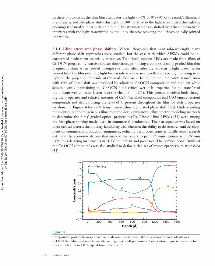
2.1.1. I-line attenuated phase shifters. When lithography first went subwavelength, manydifferent phase shift approaches were studied, but the ease with which APSMs could be in-corporated made them especially attractive. Traditional opaque BIMs are made from films ofCr-OCN prepared by reactive sputter deposition, producing a compositionally graded film thatis optically shiny when viewed through the fused silica substrate but that is light brown whenviewed from the film side. The light brown side serves as an antireflection coating, reducing straylight on the projection lens side of the mask. For use at I-line, the required 6–9% transmissionwith 180◦ of phase shift was produced by adjusting Cr-OCN composition and gradient whilesimultaneously maintaining the Cr-OCN film’s critical wet etch properties for the transfer ofthe e-beam written mask layout into the chrome film (51). This process involves both chang-ing the properties and relative amounts of CrN (metallic) compounds and CrO (antireflection)compounds and also adjusting the level of C present throughout the film for etch properties(as shown in Figure 4 for a 6% transmission I-line attenuated phase shift film). Understandingthese optically inhomogeneous films required developing novel ellipsometric modeling methodsto determine the films’ graded optical properties (52). These I-line APSMs (53) were amongthe first phase-shifting masks used in commercial production. Their acceptance was based onthree critical factors: the industry familiarity with chrome; the ability to do research and develop-ment on commercial production equipment, reducing the process transfer hurdle from research(54); and the economic drivers that enabled customers to print 250-nm features with 365-nmlight, thus delaying investments in DUV equipment and processes. The compositional family ofthe Cr-OCN compounds was also studied to define a rich set of process/property relationships(55).
Depth (Å)
Conc
entr
atio
n
C
N
O
Cr
Si
Surface
0–0.1
0.0
0.1
0.2
0.3
0.4
0.5
0.6
0.7
200 400 600 800 1000 1200 1400 1600
Figure 4Composition profiles from sputtered neutrals mass spectroscopy showing composition gradients in aCrOCN thin film used as an I-line attenuating phase shift photomask. Composition is given on an absolutebasis, which sums to 1.0. Adapted from Reference 55.
102 French · Tran
Ann
u. R
ev. M
ater
. Res
. 200
9.39
:93-
126.
Dow
nloa
ded
from
arj
ourn
als.
annu
alre
view
s.or
gby
Dr.
Rog
er F
renc
h on
07/
14/0
9. F
or p
erso
nal u
se o
nly.

ANRV380-MR39-05 ARI 27 May 2009 14:25
2.1.2. Deep UV light and 193-nm attenuated phase shifters. APSMs for 248-nm and 193-nmlithography could not be fabricated using Cr-OCN films owing to Cr’s high optical absorbance.Therefore, a materials screening study was undertaken (56), determining what two componentmaterials to use in what type of microstructure to produce the tunable optical material needed.Other researchers settled on compositionally graded films of MoSi (more accurately, compounds ofMo and Si with O, N, and C). We developed multilayer films of AlN with TiN (optical superlattices)produced by sequential multilayer ion beam deposition, in which the bilayer thickness was kept toless than λ/20 (i.e., less than 10 nm). These films were thus optically homogeneous and behavedoptically as uniform films, even though the AlN and TiN amounts in each bilayer were the variablesused to produce optical tunability (57). This material family produced APSMs with transmissionsfrom 6% to 20% with a 180◦ phase shift for both 248 and 193 nm (58). We also developedanother APSM family consisting of organic/inorganic hybrids of Teflon® AF with organosiloxanecompounds. In this case, the organosiloxane phase was used to tune the optical constants asneeded for the phase shifter design (59). These technologies were developed and evaluated by theindustry but did not reach commercialization. Materials design of new APSMs continues as anactive research field, as demonstrated by the research of Lai and colleagues (60, 61).
2.2. Polymers for Photomask Pellicles
Pellicles are thin polymer membranes supported on aluminum frames and mounted on a pho-tomask’s patterned film side—typically 6 mm above the masking film (Figure 2). They assure thatany dust particles falling onto the photomask are out of the object plane of the objective lens andtherefore are not present in the image formed in the photoresist layer by the photomask.
2.2.1. Cytop and Teflon AF. In G-line or I-line lithography, the pellicle membranes are initiallyfabricated from high-molecular-weight nitrocellulose polymers; the membrane is prepared by spincoating from a polymer solution onto a glass plate. The aluminum frame is then adhesively attachedto the polymer membrane, followed by membrane release from the glass plate, trimming of themembrane edges at the frame, and optical inspection of the pellicle for any defects. The pelliclethickness is chosen so that the membrane’s interference fringes give a maximum transmission.With the advent of DUV lithography, nitrocellulose was no longer sufficiently transparent, soamorphous fluoropolymers such as Teflon AF (62) or Cytop (from Asahi Glass Company, Tokyo),which have optical absorption edges at much shorter wavelength (Figure 5), were developed. Thethickness of the pellicle membrane can be optimized to give its peak interference transmissions atmultiple wavelengths; for example, a thickness on the order of 0.8 μm can be used for I-line andDUV lithography.
2.2.2. Novel fluoropolymers. As can be seen in Figure 5, the commercial amorphous fluo-ropolymers have appreciable absorbance at 157 nm. Films of Teflon AF 1600 and CytopTM thatare 1 μm thick have 157-nm transparency of no more than 38% and 2%, respectively, mak-ing them unsuitable for use as 157-nm pellicle materials. At the same time, a pellicle’s use is anessential requirement to enable defect free lithographic printing in a production environment.For example, EUV lithography is being pursued as a next-generation lithography, and the lack ofEUV pellicle technology is a major challenge. For 157-nm lithography, researchers developed fluo-ropolymers (63) that had optical absorption edges at much shorter wavelengths than did Teflon AF1600 or Cytop (Figure 6). Polymers such as –[(CH2CHF)xC(CF3)2CH2]y– or –(CH2CF2)x[2,2-bis(trifluoromethyl)-4,5-difluoro-1,3-dioxole]y–, with chains that alternate fluorocarbon segmentswith either oxygen or hydrocarbon segments, frequently show >98% transparency at 157 nm
www.annualreviews.org • Immersion Lithography 103
Ann
u. R
ev. M
ater
. Res
. 200
9.39
:93-
126.
Dow
nloa
ded
from
arj
ourn
als.
annu
alre
view
s.or
gby
Dr.
Rog
er F
renc
h on
07/
14/0
9. F
or p
erso
nal u
se o
nly.

ANRV380-MR39-05 ARI 27 May 2009 14:25
0150 160 170 180 190
Wavelength (nm)
Abs
orba
nce
per c
m b
ase
10 (c
m–1
)
200 210 220
1000
2000
3000
4000
5000
6000
7000
AF2400Urbach edge position = 176 nmUrbach edge width = 2.8 nm
AF1601Urbach edge position = 199 nmUrbach edge width = 5.5 nm
19
3.4
nm
AF1300Urbach edge position = 205 nmUrbach edge width = 5.9 nm
Figure 5Optical absorption edge [fits to the optical absorbance-cm−1 (base 10)] of three grades of Teflon® AF withtheir corresponding Urbach edge fits (dashed lines) showing the absorption edge position and width. Solidlines denote measured data. Adapted from Reference 62, with permission from SPIE.
(if these polymers are amorphous). These polymers are made from monomers such as vinylidenefluoride (VF2) and hexafluoroisobutylene, which themselves exhibit good structural alternationof CH2 and CF2. In addition, ether linkages can force alternation, and fluorocarbon segmentsshorter than six carbons and hydrocarbon segments shorter than two carbons (or shorter thanthree carbons if the segments are partially fluorinated), also promote 157-nm transparency. Evenwith these design principles, it is advantageous to avoid small rings such as cyclobutanes. Theseresults suggest a steric component to transparency besides the importance of alternation.
Pellicles must have long lifetimes under lithographic wavelength irradiation, given the timeand expense of repellicalization: sub–class 1 clean room, patterned mask cleaning, and new pelli-cle frame attachment. These steps may introduce new defects or even damage the patterned film.Therefore, a typical pellicle lifetime requirement corresponds to a 7.5 kJ cm−2 dose at the litho-graphic wavelength. Compared with Teflon AF 1600 and Cytop, which exhibit a pellicle lifetimeat 157 nm that is measured in millijoules, the novel fluoropolymers developed for use as 157-nmpellicles had lifetimes below 10 J cm−2.
Upon irradiation, these polymers undergo photochemical darkening, with none demonstratingthe kilojoule radiation durability lifetimes required for commercial viability. These lifetimes arelikely because the requirements are such that every bond absorbs >10 photons, each havingan energy roughly twice common bond energies. We (64) have studied intrinsic (composition,molecular weight) and extrinsic (trace metals, impurities, environmental contaminants, oxygen,water) contributions to optical absorption and photochemical darkening in these polymers. Studiesin model molecules illustrate the dynamics of photochemical darkening and show that appreciablelifetimes can be achieved in fluorocarbons. To a first approximation, the polymers that have lower157-nm optical absorbance also tend to show the longest lifetimes. These results imply thatquantum yield, or the extent to which the polymer structure can harmlessly dissipate energy, can
104 French · Tran
Ann
u. R
ev. M
ater
. Res
. 200
9.39
:93-
126.
Dow
nloa
ded
from
arj
ourn
als.
annu
alre
view
s.or
gby
Dr.
Rog
er F
renc
h on
07/
14/0
9. F
or p
erso
nal u
se o
nly.

ANRV380-MR39-05 ARI 27 May 2009 14:25
0.00
0.04
0.08
0.12
0.16
0.20
0.24
0.28
140 150 160 170 180 190 200
Abs
orba
nce
per m
icro
n ba
se 1
0 (μ
m–1
)
Wavelength (nm)
15
7 n
m
VF
2:H
FP
(7
9:2
1)
VF
2:C
TF
E (
55
:45
)
VF
2:P
MV
E (
56
:44
)
VF
2:P
PV
E (
56
:44
)
VF
2:P
DD
(6
0:4
0)
VF
2:P
MD
(4
6:5
4)
Figure 6Absorption edges of experimental TAFx fluoropolymers. Optical absorption edge of vinylidene fluoridecopolymers, with their monomer ratios in parentheses, showing low absorbance at 157 nm. The opticalabsorbance spectra [in units of 1 per micrometer (base 10) versus wavelength] show the effects oftransmission measurement saturation, as evidenced by a plateau at higher absorbance values and shorterwavelengths (owing to the low transmission of the samples at these wavelengths). This figure, andinformation on more copolymers, can be found in Reference 63, with permission from Elsevier.
be important as well (65). In parallel with developing polymeric pellicles, fused silica glass pellicleswere developed and showed promising optical performance.
3. MATERIALS IN THE LITHOGRAPHIC IMAGING STACK
The immersion lithography materials required on the image side (i.e., below the projection lens)also span a wide variety of materials and classes. These materials include the immersion fluids,topcoats (used to separate the fluid from the imaging photoresist film), the photoresist layer, andan antireflection layer underneath. We discuss these in order below.
3.1. Immersion Fluids
Immersion fluids yield enhanced imaging performance in the same way that water or oil immersiontechniques improve an optical microscope’s resolution. When imaging is performed in a fluid thathas a refractive index of >1 (1 is the value for air), the light’s wavelength is effectively reducedby the fluid’s index. The fluids must be optically transparent (i.e., have a low optical absorbanceat the lithography wavelength) and must have a high refractive index. The first immersion fluidsstudied were to be used to extend 157-nm lithography, but it is immersion lithography at 193 nmusing water that has been successfully commercialized.
Water-based immersion lithography using 193-nm ArF illumination provides optical solu-tions as far as the 45-nm node (with a k1 of 0.31) but is not able to achieve the 38-nm or 32-nm
www.annualreviews.org • Immersion Lithography 105
Ann
u. R
ev. M
ater
. Res
. 200
9.39
:93-
126.
Dow
nloa
ded
from
arj
ourn
als.
annu
alre
view
s.or
gby
Dr.
Rog
er F
renc
h on
07/
14/0
9. F
or p
erso
nal u
se o
nly.

ANRV380-MR39-05 ARI 27 May 2009 14:25
nodes as currently defined. Achieving these lithographic nodes will require new, higher-refractive-index fluids to replace the water used in first-generation immersion systems. Therefore, therehas been extensive research to develop second-generation (1.44 ≤ n193 nm ≤ 1.65) and third-generation (1.65 ≤ n193 nm ≤ 1.8) 193-nm immersion fluids. We have developed a number of suchsecond-generation high-index fluids for immersion lithography at 193 nm, with low optical ab-sorbance and refractive indices up to 1.664. To understand different fluid classes’ behavior andperformance, we use spectral index measurements to characterize the index dispersion, coupledwith Urbach (66) absorption edge analysis and Lorentz oscillator modeling (34).
Compared with water (a ubiquitous liquid of relatively low cost and high ease of disposal), asecond- or third-generation high-index immersion fluid will require methods for recycle, so itscosts can be spread over a larger number of wafers imaged. Therefore, we also discuss below thefluids’ radiation durability and at-stepper recycle technology performance to permit these fluids’reuse.
3.1.1. Fluids at 157 nm. Studies of model small molecule fluids’ photochemistry that were thefocus of 157-nm pellicle radiation durability studies led to the development of 157-nm immersionfluid research. Various fluid classes were identified with low optical absorbance at 157 nm and withreasonable photochemical durability. These small-molecule fluids were therefore the initial candi-dates for 157-nm immersion fluids. We pursued broader-based studies on more than 50 candidate157-nm immersion fluids to identify fluid classes appropriate for 157-nm imaging (67). Thesefluids’ optical absorbances have both intrinsic and extrinsic contributions, so purification methodssuch as degasification, distillation, and supercritical fluid fractionation were investigated to deter-mine residual contaminants’ impact on absorbance. In most cases, the absorbance was dominatedby dissolved oxygen and water in the fluid. Once these contaminant levels are reduced, the mosttransparent perfluoroether (PFE) measured was perfluoro-1,2-bis(2-methoxyethoxy)ethylene gly-col (perfluorotriglyme), which has a 157-nm optical absorbance of 0.52 cm−1; the most trans-parent perfluoroalkane (PFA) measured was perfluorohexane at 1.1 cm−1; the most transparenthydrofluoroether (HFE) was 1-(1H-tetrafluoro)ethoxy-2-(1-trifluoromethyl)tetrafluoroethoxy-2-trifluoromethyl-1,1,2-trifluoroethane at 2.6 cm−1; and the lowest projected absorption coef-ficient for a hydrofluoroalkane (HFA) was decafluoro-2H,3H-pentane at <2 cm−1. Our chemicalanalysis showed that some impurities still remained in these materials, and so further reductions inabsorption are possible. Even so, our current absorption values should allow lens-to-wafer work-ing distances (assuming 95% transmission) of 428 nm, 203 nm, 83 nm, and 111 mm, respectively,for the four fluid classes. The identification of these four fluid classes (PFEs, PFAs, HFEs, andHFAs) for potential use as 157-nm immersion fluids—each with their own ranges of viscosity,vapor pressure, refractive index, dn/dT, synthetic routes, and cost—should allow for flexibility inperforming trade-off analyses for various 157-nm immersion lithography engineering designs andcost-of-ownership estimates.
Because 157-nm “dry” lithography did not commercialize, the research in 157-nm immersionfluids stopped at this stage. From the following discussion of 193-nm immersion fluids, it isapparent that this research was only an initial step in defining an appropriately transparent fluidfor 157-nm lithography. These fluids’ indices, their radiation durabilities, their photochemicalstabilities in use, and methods for recycle would all have required additional research.
3.1.2. Fluids at 193 nm. The largest NA for a water-based immersion scanner is the NA = 1.35of the ASML XT:1950i shown in Figure 1; this projection lens has a dry NA ∼ 0.93. Researchon second-generation immersion fluids—whose 193-nm indices of 1.65 would enable scannerswith NAs on the order of 1.55—requires identifying not just a high-index fluid with low 193-nm
106 French · Tran
Ann
u. R
ev. M
ater
. Res
. 200
9.39
:93-
126.
Dow
nloa
ded
from
arj
ourn
als.
annu
alre
view
s.or
gby
Dr.
Rog
er F
renc
h on
07/
14/0
9. F
or p
erso
nal u
se o
nly.
ANRV380-MR39-05 ARI 27 May 2009 14:25
optical absorbance, but also a fluid with high radiation durability and technology for fluid recycleand reuse at the stepper to meet the industry’s fluid-cost-of-ownership goal of $1–2 per wafer levelimaged. We discuss these aspects of immersion fluid research here.
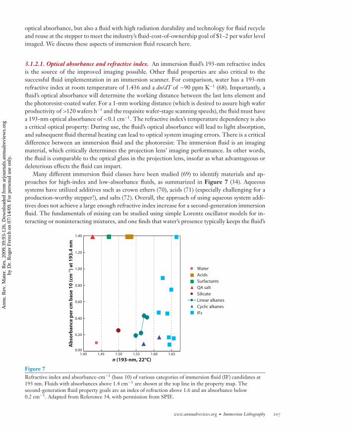
3.1.2.1. Optical absorbance and refractive index. An immersion fluid’s 193-nm refractive indexis the source of the improved imaging possible. Other fluid properties are also critical to thesuccessful fluid implementation in an immersion scanner. For comparison, water has a 193-nmrefractive index at room temperature of 1.436 and a dn/dT of −90 ppm K−1 (68). Importantly, afluid’s optical absorbance will determine the working distance between the last lens element andthe photoresist-coated wafer. For a 1-mm working distance (which is desired to assure high waferproductivity of >120 wafers h−1 and the requisite wafer-stage scanning speeds), the fluid must havea 193-nm optical absorbance of <0.1 cm−1. The refractive index’s temperature dependency is alsoa critical optical property: During use, the fluid’s optical absorbance will lead to light absorption,and subsequent fluid thermal heating can lead to optical system imaging errors. There is a criticaldifference between an immersion fluid and the photoresist: The immersion fluid is an imagingmaterial, which critically determines the projection lens’ imaging performance. In other words,the fluid is comparable to the optical glass in the projection lens, insofar as what advantageous ordeleterious effects the fluid can impart.
Many different immersion fluid classes have been studied (69) to identify materials and ap-proaches for high-index and low-absorbance fluids, as summarized in Figure 7 (34). Aqueoussystems have utilized additives such as crown ethers (70), acids (71) (especially challenging for aproduction-worthy stepper!), and salts (72). Overall, the approach of using aqueous system addi-tives does not achieve a large enough refractive index increase for a second-generation immersionfluid. The fundamentals of mixing can be studied using simple Lorentz oscillator models for in-teracting or noninteracting mixtures, and one finds that water’s presence typically keeps the fluid’s
0.001.40 1.45 1.50 1.55 1.60 1.65
0.20
0.40
0.60
0.80
1.00
1.20
1.40
n (193-nm, 22°C)
Abs
orba
nce
per c
m b
ase
10 (c
m–1
) at 1
93.4
nm
Water
Acids
Surfactants
QA salt
Silicate
Linear alkanes
Cyclic alkanes
IFs
Figure 7Refractive index and absorbance-cm−1 (base 10) of various categories of immersion fluid (IF) candidates at193 nm. Fluids with absorbances above 1.4 cm−1 are shown at the top line in the property map. Thesecond-generation fluid property goals are an index of refraction above 1.6 and an absorbance below0.2 cm−1. Adapted from Reference 34, with permission from SPIE.
www.annualreviews.org • Immersion Lithography 107
Ann
u. R
ev. M
ater
. Res
. 200
9.39
:93-
126.
Dow
nloa
ded
from
arj
ourn
als.
annu
alre
view
s.or
gby
Dr.
Rog
er F
renc
h on
07/
14/0
9. F
or p
erso
nal u
se o
nly.

ANRV380-MR39-05 ARI 27 May 2009 14:25
2
4
6
8
10
12
14
16
18
Wavelength (nm)
Abs
orba
nce
per c
m b
ase
10 (c
m–1
)
165 170 175 180 185 190 195 200
Wavelength (nm)
Figure 8Optical absorbance-cm−1 (base 10) for various alkane immersion fluid candidates. Figure courtesy ofCostner et al. (76). Adapted from Reference 34, with permission from SPIE.
193-nm index below approximately 1.58 (34). Organic fluids, such as the linear and cyclic alkanes,can achieve both the necessary high 193-nm index and the low 193-nm optical absorbance (73)and have been the focus of much study (74–77). Linear alkanes versus cyclic alkanes exhibit a lowerrefractive index for a comparable number of carbon atoms in the former, leading to a focus on thelatter class. Costner et al. (76) show the trends in the optical absorption edge position for bothlinear and cyclic alkanes (Figure 8); as the number of carbon rings increases, the optical absorptionedge shifts to longer wavelengths. There has also been work on nanoparticle approaches to third-generation fluids (78), and progress has been reported from fluids using high-index nanoparticlessuch as HfO2.
One of the best second-generation immersion fluid candidates is IF132, which has opticalabsorbance at 193 nm ∼ 0.03 cm−1 (comparable to water’s absorbance) and a 193-nm refractiveindex of 1.644. We also identified other fluids such as IF169 with an index of 1.656 and others withindices approaching 1.68 at 193 nm. It is instructive to compare the indices of water and IF132(Figure 9): IF132 has an index at 589.3 nm (the sodium d-line wavelength) of 1.484, which ishigher than water’s index at this wavelength. If we define the index dispersion �n as the differencein the index from 193 nm to 589 nm, then the dispersion of IF132 is 0.160, whereas water exhibitsa dispersion of only 0.103. So in some ways, water is a rather low-index fluid, with relatively lowdispersion when compared with second-generation immersion fluids. Another major difference
108 French · Tran
Ann
u. R
ev. M
ater
. Res
. 200
9.39
:93-
126.
Dow
nloa
ded
from
arj
ourn
als.
annu
alre
view
s.or
gby
Dr.
Rog
er F
renc
h on
07/
14/0
9. F
or p
erso
nal u
se o
nly.

ANRV380-MR39-05 ARI 27 May 2009 14:25
190
1.70
1.65
1.60
1.55
1.50
1.45
1.40
1.35
240 290 340 390
Wavelength (nm)In
dex
of re
frac
tion
, n440 490 540 590
IF132: IF132: n(193-nm) = 1.6439(193-nm) = 1.6439
n(d-line) = 1.3320(d-line) = 1.3320 Water: ΔWater: Δn = 0.1046 = 0.1046
IF132: ΔIF132: Δn = 0.1661 = 0.1661n(d-line) = 1.4778(d-line) = 1.4778
Water: Water: n(193-nm) = 1.4366(193-nm) = 1.4366
IF132: n(193-nm) = 1.6439
n(d-line) = 1.3320 Water: Δn = 0.1046
IF132: Δn = 0.1661n(d-line) = 1.4778
Water: n(193-nm) = 1.4366
Figure 9Spectral index of refraction versus wavelength of IF132 compared with water. Note IF132’s increased n(d-line), dispersion �n, and n (193 nm). Adapted from Reference 34, with permission from SPIE.
in the optical properties of water versus second-generation fluids is in the index temperaturedependency. Here, water has an anomalously low dn/dT of −93 × 10−6 K−1, whereas IF132has dn/dT = −550 × 10−6 K−1—an increase of more than 5 × (79). This fluid temperaturedependency leads directly to a more accurate temperature control requirement in an immersionscanner using a second-generation fluid. It was also essential to study any other sources of variabilityin the fluids’ optical properties. We therefore determined the variations of index, and �n/�λ ofIF132 and IF169, for different batches of fluid (within a 6-mo period), before-and-after irradiation(at 193.4 nm), before-and-after air exposure, and before-and-after resist exposure (image printingtest). We found these changes to be not critical for system design.
3.1.2.2. Radiation durability and recycling. Following the development of viable second-generation immersion fluids such as IF132, it became essential to examine other property/processrequirements relevant to commercial use, such as fluid radiation durability, last lens element con-tamination and cleaning, and (as discussed in the next section) resist interactions and profile effects.These studies show that both fluid handling issues as well as active fluid recycling must be wellunderstood and carefully managed to maintain optimum fluid properties.
The radiation durability of second-generation immersion fluids, and their increased cost com-pared with the cost of water, requires that the fluids be recycled. A desirable approach is fluid recycleat the stepper, actively removing any photochemical degradation products during use—a processwe call active recycle. The recycling methods’ efficacy directly impacts the cost of ownership ofhigh-index immersion lithography. It is therefore essential to develop a detailed understanding ofradiation durability: how realistic exposure conditions (in a high-index immersion scanner) willimpact both the immersion fluid and the scanner’s last lens element. We have therefore developeddetailed input and output metrics for both the fluids and the windows used in radiation durabilitytests, so these results can be cross-correlated to standard stepper conditions (80). Under suchconditions, a typical fluid would be exposed to 6 J cm−2 in 1 week, and the last lens element wouldsee a 60 kJ cm−2 dose per day. These magnitude differences are related to the fact that the fluid iscirculating and the full fluid volume is not continuously irradiated, whereas the last lens elementis continuously irradiated.
Using a fluid circulation system (Figure 10), we performed laboratory-scale experiments,in which the fluid was recirculated under 193-nm laser irradiation conditions mimicking thefluid’s exposure in the standard stepper. Thus, the active-recycle system’s efficiency in remov-ing photodegradation products from the fluid could be determined in situ. We performed op-tical absorbance measurements on the laser irradiation cell, which determines the induced cell
www.annualreviews.org • Immersion Lithography 109
Ann
u. R
ev. M
ater
. Res
. 200
9.39
:93-
126.
Dow
nloa
ded
from
arj
ourn
als.
annu
alre
view
s.or
gby
Dr.
Rog
er F
renc
h on
07/
14/0
9. F
or p
erso
nal u
se o
nly.

ANRV380-MR39-05 ARI 27 May 2009 14:25
Fluidcylinder
N2
Active recyclepackage
Spectrometer cell
Pump
Vent
N2
Laser exposure cell
Figure 10Schematic of the fluid circulation system. Figure adapted from Reference 80, with permission from SPIE.
absorbance, and on a second fluid absorbance spectroscopy cell, which determines the inducedfluid absorbance. With these two results, we independently measured the fluid-induced absorbancerate and the window-induced absorbance rate to determine the rates of fluid and window darkeningin use.
From a series of experiments, we determined the fluid’s induced absorbance rate was0.079 cm J−1 for IF132 without active recycle. The induced absorbance rate for other second-generation immersion fluids can be 50× to 100× higher than this IF132 result. Then, using twodifferent active-recycle versions (versions 3 and 4), we found that the fluid’s induced absorbancerate was decreased by a factor of 3× and 9× (Figure 11), leading to an increase in the fluid’susable life in the standard stepper to nine days.
In addition to the work on fluid recycling, there has been active fluid dynamics research on thefluid’s flow over the wafer, under the projection lens. This research is useful both for issues such
0
0.1
0.2
0.3
0.4
0.5
0 1 2 3 4 5 6 7 8 9 10
Fluid dose (J cm–2)
IF132 (no ARP)
IF132 (version 3 ARP)
IF132 (version 4 ARP)
No ARP
With ARP
3X
9X
Indu
ced
fluid
(abs
orba
nce
cm–1
)
Figure 11Induced fluid absorbance versus fluid dose for IF132, studied with no active-recycle package (ARP) and withtwo different versions that reduce the fluid’s photochemical darkening rate by factors of 3× and 9× . Theseare averages of five experiments for each case.
110 French · Tran
Ann
u. R
ev. M
ater
. Res
. 200
9.39
:93-
126.
Dow
nloa
ded
from
arj
ourn
als.
annu
alre
view
s.or
gby
Dr.
Rog
er F
renc
h on
07/
14/0
9. F
or p
erso
nal u
se o
nly.

ANRV380-MR39-05 ARI 27 May 2009 14:25
as vibration control (81) and also for the possible introduction of fluid-flow-induced bubbles (orbubble entrapment from wafer topography), which can lead to imaging defects (82).
3.1.3. Immersion fluid–resist interactions. Using water or another higher-index-matchingliquid between the last lens element and the photoresist introduces new issues not previouslyencountered in conventional dry lithography. Much of the early work identified the key issuesrelated to imaging under water immersion (83), and later, the same issues were addressed for thehigher-index organic liquids (84). Of particular concern is the extent of resist components’ extrac-tion from the resist film into the immersion liquid. Components in the resist formulation suchas PAGs and their photogenerated acids, dissolution modifiers, and bases may all leach from thefilm. The amount of leaching is of course a function of the resist film’s component concentration,the rate of the components’ diffusion into the liquid, the solubility of the components, and thetime of fluid/resist contact. Leaching has two effects. First, the resist’s imaging properties, such assensitivity, are changed, and performance is usually degraded. Second, leached components, es-pecially PAGs, may undergo further photochemistry and adsorb onto the system optics (85, 86), atopic of particular concern to the stepper manufacturers—which has led to their setting maximumtolerable PAG limits on the order of 1.0–5.0 × 10⁻¹² mol (cm2-s)−1. The PAG amount detectedin water for some commercially available resists has either come very close to or exceeded thislimit (87–90). This result has prompted further work on designing immersion topcoats or top-coatless resists (vide infra) to slow or prevent leaching. It has also led to work to prerinse the resistsurface with water [because most of the PAG leaching occurs in the first few seconds of contact(91)], which has been reported to remove more than 90% of the PAG at the water-resist interface.With second-generation immersion fluids, very little PAG leaching has been detected, reportedlyapproximately two orders of magnitude lower than the recommended limit (see Figure 12).
Another key immersion imaging issue is the effect of fluid penetration into the resist film.Subsurface immersion liquid may modify the kinetics of the acid-catalyzed deprotection reaction(especially if water carries with it species that can quench photoacid). It can also act as a polymerfilm plasticizer (especially true for organic liquids diffusing into organic resist polymers), changingthe film’s mechanical properties and diffusion-related properties. With water as the immersionfluid, quartz crystal microbalance and optical reflectance techniques have shown that 200-nm
a TARF-Pi6-001 resist
0.00
1.00
2.00
3.00
4.00
5.00
6.00
7.00
8.00
9.00
10.00
Water IF132 IF169 Blank Water IF132 IF169 Blank
Det
ecte
d PA
G (1
0–10 m
ol m
L–1)
Det
ecte
d PA
G (1
0–10 m
ol m
L–1)Test 1
Test 2
b Water immersion CH resist
0.00
1.00
2.00
3.00
4.00
5.00
6.00
7.00
8.00
9.00
10.00
Test 1
Test 2
Figure 12Amount of photoacid generator (PAG) leached in 6 min from two water-specific immersion resists into IF132 and IF169. No PAG wasdetected in the high-index liquids.
www.annualreviews.org • Immersion Lithography 111
Ann
u. R
ev. M
ater
. Res
. 200
9.39
:93-
126.
Dow
nloa
ded
from
arj
ourn
als.
annu
alre
view
s.or
gby
Dr.
Rog
er F
renc
h on
07/
14/0
9. F
or p
erso
nal u
se o
nly.

ANRV380-MR39-05 ARI 27 May 2009 14:25
films may swell up to 5 nm in thickness (83). There is also some evidence that second-generationimmersion fluids cause up to 2 nm in initial swelling, and up to 10 nm of dissolution, of somecommercial resists (84). Despite these observations, there seem to be only subtle effects on sub-45-nm line and space interference imaging of some commercially available resists with both waterand second-generation immersion fluids (vide infra).
Both resist component extraction into the immersion fluid, and fluid permeation into theresist, may cause unwanted defects in the final resist image, and much work has been done toquantify and reduce the new defect types seen under immersion imaging (92–94). These defecttypes may be classified into five general categories: process-induced defects, watermark defects,defects arising from bubbles in the fluid, drying stain defects, and particle-borne defects. Defectsrelated to processing may originate from fluid-carrying particles from the wafer edge, especiallyif the topcoat, resist, or BARC peels at the edge, and the fluid is scanned beyond this edge point.Steps to rinse and clean the bevel have shown marked improvement in defect counts. Fluidsthat permeate into the resist film can generate watermark defects, which include swelling oflines and T-topping. Bubbles (which may originate from gaseous by-products from the resist orentrapment of bubbles from fast scanning at the advancing edge of the fluid-resist interface) may bea source of undeveloped resist regions. Resist component leaching into the fluid, in conjunctionwith fluid droplet evaporation, may lead to drying stain defects. Drying stain defects are alsopossible if the fluid is not pure, with evaporation leading to surface residues. Finally, fluid orenvironmental particles can cause printed defects if present during exposure. Optimization inboth processing and immersion-related materials is necessary to improve defect performance.These improvements have resulted in defect densities below 0.06 cm−2 for water immersion.For high-index immersion, preliminary defect studies have concentrated on both the high-indexfluids, cleanliness and fluid-misted droplets’ interaction with several commercially available dryand water immersion photoresists (95). Misted defect counts of a high-index fluid, designatedIF132, have shown acceptable numbers for further optimization. Experiments in which the resistis soaked with the fluid before and after exposure show that the printed 90-nm lines do not varysignificantly in lateral line dimension, with only a slight resist thickness loss.
3.2. Immersion Topcoats and Photoresists
Although some topcoats and photoresists for dry lithography can be used, optimal imaging per-formance is only obtained when these materials are specifically optimized for immersion imaging.In this section, research on novel topcoats, topcoatless photoresists, and high-index photoresistsfor third-generation immersion lithography are discussed.
3.2.1. Topcoats and topcoatless photoresists. Fears of lens contamination, increased defects,and resist performance degradation with water immersion lithography prompted much researchactivity on novel topcoats and the so-called topcoatless photoresists. Topcoats are designed toreduce both water permeation into the photoresist as well as resist component leaching (espe-cially PAG) and also to increase water’s receding contact angle at fast scan speeds (to reducewater droplet formation that may lead to imaging defects). More hydrophobic topcoats providethe increased receding contact angle to allow higher scanning velocities before droplet formationoccurs (82). Topcoats showing more than 100◦ receding contact angles will enable speeds up to900 mm s−1. Ideally, the topcoat would dissolve in the same aqueous base developer (TMAH)used in the resist development step, but some topcoat versions were designed for nonaqueoussolvent development, which adds an extra processing step. Many topcoats incorporate fluorine-containing functional groups for their increased hydrophobicity, as well as the same compound
112 French · Tran
Ann
u. R
ev. M
ater
. Res
. 200
9.39
:93-
126.
Dow
nloa
ded
from
arj
ourn
als.
annu
alre
view
s.or
gby
Dr.
Rog
er F
renc
h on
07/
14/0
9. F
or p
erso
nal u
se o
nly.

ANRV380-MR39-05 ARI 27 May 2009 14:25
types used effectively for absorbance reduction in 157-nm technology (88, 96–101). These fluo-ropolymers have also been used in water immersion resist materials—either as additives to current193-nm materials or as block copolymers (102–104). These systems are designed so that a topcoatis not necessary, but instead incorporate the topcoat’s hydrophobic properties directly into thephotoresist, eliminating an extra topcoat spinning step. These topcoatless resists depend on theself-segregation of low-surface-energy fluoro-components to the air interface during spinning andbaking, providing the needed hydrophobicity for water immersion imaging. A novel method tomake the block copolymers relies on RAFT polymerization to make the first block composed of193-nm photoresist monomers, followed by a second block composed of a fluorinated monomer.Blends of this block copolymer (even at very small fractions) with a standard nonfluorinatedmethacrylate terpolymer show high receding contact angles. One variant to this system, whichmay further reduce the defect levels, involves modifying the fluorinated block to be developersoluble—which would also help with developer wettability.
3.2.2. High-index photoresists for third-generation immersion. Current 193-nm photore-sists have refractive indices of approximately 1.7, which would be the limiting index in the op-tical path if a higher-refractive-index fluid (∼1.8) and LuAG (lutetium aluminum garnet, with a193 nm index of 2.14, as the last lens element) were used. Thus, there has been some research effortto predict, screen, and synthesize materials possessing both a target refractive index of 1.9 andthe required absorbance below 3 μm−1 (105, 106). Quantitative structure property relationship(QSPR) modeling was developed from a database of hundreds of organic compounds to predictrefractive indices at 589 nm (107). This information, along with knowledge of the refractive indexdispersion, was used to show that molecules with high molecular weight, high heat of formation,high sulfur contents, and low fluorine and hydrogen contents increase refractive index at 193 nm.Other researchers have taken this information to design and synthesize imageable resist polymerscontaining thioacetal, thioester, and sulfone groups, with absorbance edges near 193 nm [for bothhigh refractive index and low absorption (108)]. One particular copolymer, incorporating both anadamantyl methacrylate as well as a methacrylate having both a thioester and sulfone functionality,has a refractive index above 1.8 and an absorbance below 1.4 μm−1 and was successfully imagedto produce 110-nm lines and spaces.
4. IMMERSION LITHOGRAPHY IMAGING PERFORMANCE AT 193 NM
4.1. Comparative Water and Second-Generation Fluid Imaging
In this section, we highlight work done to compare water-based and high-index fluid-based imag-ing. Because no water immersion tools were available early in immersion development, researchersrelied on soaking experiments to provide a sense of the imaging capability of the most current193-nm dry resists, using production-worthy dry 193-nm tools. The resist films were soaked withwater before and after exposure and then processed normally (88, 109). The same experimentswere performed using high-index fluids, and the 90-nm resist profiles were compared (using scat-terometry metrology) for each fluid on three commercially available resists: a dry line-space resist,a water immersion line-space resist, and a water immersion contact hole resist (Figure 13). Eachfluid had its own subtle effects on each resist. For example, water tended to provide thicker andwider resist profiles on the dry resist (presumably owing to resist component extraction such asPAG), but the same effect was lessened on a water immersion–dedicated resist. The high-indexfluid IF132 was observed to thin the resist profiles after postexposure soak. Although the resistprofiles were affected by direct fluid contact, researchers concluded that the improvements made
www.annualreviews.org • Immersion Lithography 113
Ann
u. R
ev. M
ater
. Res
. 200
9.39
:93-
126.
Dow
nloa
ded
from
arj
ourn
als.
annu
alre
view
s.or
gby
Dr.
Rog
er F
renc
h on
07/
14/0
9. F
or p
erso
nal u
se o
nly.

ANRV380-MR39-05 ARI 27 May 2009 14:25
a PAR-817
–15
–10
–5
0
5
10
15
Water
Pre
Water
Post
IF132
Pre
IF132
Post
IF169
Pre
IF169
Post
Del
ta to
dry
exp
osur
e(n
m, d
egre
es)
–15
–10
–5
0
5
10
15
Del
ta to
dry
exp
osur
e(n
m, d
egre
es)
–15
–10
–5
0
5
10
15
Del
ta to
dry
exp
osur
e(n
m, d
egre
es)
b TArF-Pi6-001
Water
Pre
Water
Post
IF132
Pre
IF132
Post
IF169
Pre
IF169
Post
c Water Immersion CH Resist
Water
Pre
Water
Post
IF132
Pre
IF132
Post
IF169
Pre
IF169
Post
Middle CD
Resist thickness
Sidewall angle
Figure 13Delta between scatterometry parameters for a dry reference wafer and wafers soaked preexposure (pre) or postexposure (post).
in the most current water immersion–dedicated resists also had a positive effect on the high-indexfluids’ imaging.
4.2. Interference Imaging
Interference imaging printers have long been available but now have a new use: a rapid, cost effec-tive way to develop immersion lithography, particularly at extremely high resolutions. Althoughinterference printers will never replace classical lens-based lithography systems for semiconduc-tor device production, they do offer a means to develop resist and fluid technology at relativelylow cost. Their simple image-forming format (shown in Figure 14 for dual-beam interferenceimaging) offers easy access to the basic physics of advanced imaging. Issues such as polarization ofthe image-forming light rays, fluid-resist interaction during exposure, topcoat film performance,and resist LER at extremely high resolutions can all be readily studied.
Interference printing of several commercial resists that are fully submersed in either water ora high-index fluid during exposure has been demonstrated, providing resolutions beyond currentlens-based system capabilities (95, 109–111). In early development, lines with dimensions as low
114 French · Tran
Ann
u. R
ev. M
ater
. Res
. 200
9.39
:93-
126.
Dow
nloa
ded
from
arj
ourn
als.
annu
alre
view
s.or
gby
Dr.
Rog
er F
renc
h on
07/
14/0
9. F
or p
erso
nal u
se o
nly.

ANRV380-MR39-05 ARI 27 May 2009 14:25
Beam splitterBeam splitterBeam splitter
Line and space exposures
Figure 14Two-beam interferometric imager. Sin(θ) and hence resolution are set by adjusting the positions and anglesof the mirrors. Adapted from Reference 34, with permission from SPIE.
as 32 nm were printed using a dry, commercially available resist submersed in IF132 in a two-beaminterferometer (112). In later experiments, 36-nm half-pitch lines were printed to directly comparewater immersion imaging and high-index immersion imaging (because water immersion allowsonly printing of half pitches down to 34 nm on the basis of current processing optimizations withNA of 1.35). Figure 15 shows the top-down and cross-sectional scanning electron micrographs(SEMs) of the lines obtained for one dry (PAR-817) and two water immersion–dedicated resistsusing water and two high-index fluids. The improvements made for the water immersion resistswere evident in the imaging: Clean 36-nm lines and spaces were obtained under water as wellas under the two high-index fluids. Lines with dimensions as small as 29 nm were even obtainedwith the two immersion-dedicated resists using IF132 as the immersion fluid (Figure 16). Theseimaging tests demonstrate the great strides made in resist performance and the compatibility ofcommercially available resists with both water and high-index fluids; with further process andmaterial optimizations, line dimensions to 32 nm can be printed with the higher-index fluids.
5. DOUBLE-PATTERNING METHODS
Strategies to further increase resolution by optical means alone may have been exhausted becausedecreasing the wavelength beyond 193 nm leads to EUV lithography, a nonoptical method thathas several major unresolved problems. Also, increasing the NA to 1.55 with high-index fluidswill allow patterning down to only 32-nm half pitch, even at the most aggressive k factors. Themost likely alternative would be some form of double patterning, in one variation of which thedesired patterns are split between two masks, such that more facile feature printing is done attwice the pitch. The second mask would be aligned so that the second feature set is printedbetween the first set, providing final features with target dimensions at the desired half pitch.This takes advantage of the fact that one can image smaller features more easily if the pitch is
www.annualreviews.org • Immersion Lithography 115
Ann
u. R
ev. M
ater
. Res
. 200
9.39
:93-
126.
Dow
nloa
ded
from
arj
ourn
als.
annu
alre
view
s.or
gby
Dr.
Rog
er F
renc
h on
07/
14/0
9. F
or p
erso
nal u
se o
nly.
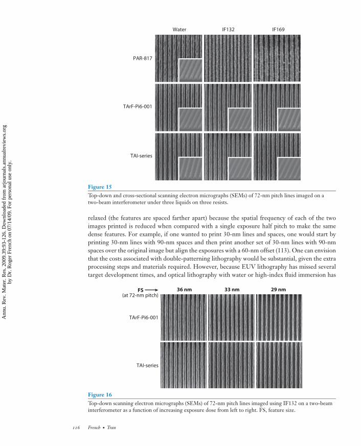
ANRV380-MR39-05 ARI 27 May 2009 14:25
Water IF132 IF169
PAR-817
TArF-Pi6-001
TAI-series
Figure 15Top-down and cross-sectional scanning electron micrographs (SEMs) of 72-nm pitch lines imaged on atwo-beam interferometer under three liquids on three resists.
relaxed (the features are spaced farther apart) because the spatial frequency of each of the twoimages printed is reduced when compared with a single exposure half pitch to make the samedense features. For example, if one wanted to print 30-nm lines and spaces, one would start byprinting 30-nm lines with 90-nm spaces and then print another set of 30-nm lines with 90-nmspaces over the original image but align the exposures with a 60-nm offset (113). One can envisionthat the costs associated with double-patterning lithography would be substantial, given the extraprocessing steps and materials required. However, because EUV lithography has missed severaltarget development times, and optical lithography with water or high-index fluid immersion has
36 nm 33 nm 29 nm
TArF-Pi6-001
TAI-series
FS(at 72-nm pitch)
Figure 16Top-down scanning electron micrographs (SEMs) of 72-nm pitch lines imaged using IF132 on a two-beaminterferometer as a function of increasing exposure dose from left to right. FS, feature size.
116 French · Tran
Ann
u. R
ev. M
ater
. Res
. 200
9.39
:93-
126.
Dow
nloa
ded
from
arj
ourn
als.
annu
alre
view
s.or
gby
Dr.
Rog
er F
renc
h on
07/
14/0
9. F
or p
erso
nal u
se o
nly.
ANRV380-MR39-05 ARI 27 May 2009 14:25
Doubleexposure
Resist coat
First exposure
Second exposure
Development
Doubledevelopment
Exposure
First development
Second development
Freezing
First resist coat
First exposure
Freezing
Second resist coat
Second exposure
Second development
Sidewall
Resist coat
Exposure
Development
Etching
Sidewall form
Deposition
CMP
Etching
Resist coat
Exposure
Development
Etching
Resist coat
Exposure
Development
Etching
Resist coat
Exposure
Development
Etching
Resist coat
Exposure
Development
Etching
Double line Double trench
Resist coat
First development
Figure 17Approaches for double-patterning lithography. Approaches increase in complexity of processing steps from left to right: The leastcomplex (but most material-demanding) approach is at the left, and the most complex process (but least material-demanding) approachis at the right. CMP, chemical mechanical planarization or chemical mechanical polishing. Figure from Tarutani-san, Fujifilm. Adaptedfrom Semiconductor International Webcast on Preparing for High-Volume Immersion Lithography (121).
shown much potential, applying some double-patterning method to immersion lithography wouldprovide a means to further resolution improvements to keep pace with integrated circuits’ leading-edge feature size requirements.
Several industrial laboratories and academic institutions are developing their own approachesfor accomplishing this double-patterning task. Figure 17 schematically shows a few such ap-proaches (114). The last two columns depict the double-patterning method described above, inwhich two exposure steps, two development steps, and two etching steps are required for pitchdoubling. This method’s costs have prompted researchers to scout other alternatives that couldeliminate some of the extra processing steps. The most challenging approach is a double-exposuremethod shown in the first column of Figure 17. In this method, the two mask patterns are exposedconsecutively into the same material, providing better overlay accuracy (because the wafer is notremoved from the scanner chuck). This requires a material that can behave in an optically nonlin-ear manner, and to date no such material exists, although some conceptual and simulation workhas been reported (115–118). The material must “forget” subthreshold exposure doses in the first
www.annualreviews.org • Immersion Lithography 117
Ann
u. R
ev. M
ater
. Res
. 200
9.39
:93-
126.
Dow
nloa
ded
from
arj
ourn
als.
annu
alre
view
s.or
gby
Dr.
Rog
er F
renc
h on
07/
14/0
9. F
or p
erso
nal u
se o
nly.

ANRV380-MR39-05 ARI 27 May 2009 14:25
exposure pass before the second one; otherwise, the two individual mask images are not resolved.Many current photosensitive materials possess this memory effect: Subthreshold exposure in thefirst pass reduces the dose required for chemical change in the second one. First-order phasetransitions, in contrast, show no memory effect because the same energy amount is required toheat a material to the melt transition the second time after it has been cooled from the first heat—the transition is reversible. Several material approaches to obtain a nonlinear response to exposurehave been proposed. One of the more interesting concepts is the photoreversible topcoat, or whatis termed the contrast enhancement layer (CEL). The CEL is a thin layer of opaque material ontop of a conventional photoresist that is rapidly photobleached when illuminated at 193 nm inthe first exposure pass and then regains its opacity after illumination before the second pass. Ineffect, this topcoat would act as a reversible contact mask, allowing light to penetrate in regionswhere aerial image intensities are higher than the threshold and preventing light penetration inregions where the aerial image intensities are lower. Photochromic molecules are good candidatesfor this purpose and, depending on their chemistry, can undergo reversion by relaxation, thermal,or optical means. For example, spiropyrans and spirooxazines are colorless in the leuco form butbecome colored after irradiation, reverting back to the leuco form with heat. Other moleculeslike the diarylethenes can revert back to the original form via visible light. Work is under wayto identify photochromic systems that are effective at 193 nm, because most known systems areactive at wavelengths greater than 300 nm. This may not be an easy task because some of theother desired CEL properties may be difficult to achieve. Such desirable properties include fastfilm bleaching with a transmission optical density of 2.0 to a stable saturated optical density of0.2, using approximately 30 mJ cm−2 of 193-nm radiation; fast reversion once illumination isstopped; spin coatability over current photoresists; and the capacity for development in a standardphotoresist developer.
Two other approaches for double patterning are termed double development (or dual-tonedevelopment) and resist freezing. In double development, a hybrid resist (which is essentially amixture of a positive-tone resist and a negative-tone resist) that exhibits two solubility transitionsat the optimal exposure dose is used (119–121). As the initially insoluble hybrid resist is exposed,it reaches a threshold dose at which it becomes soluble in TMAH developer (a positive-tonecharacteristic). At higher-exposure doses, the resist reaches another threshold point at which itbecomes insoluble in solvent (a negative-tone characteristic). One must therefore match the twothreshold points to formulate a resist that provides pitch doubling from the sinusoidal aerialimage. The hybrid resist would transform at intensities higher than the threshold in a positive-tone development step and would transform at intensities lower than the threshold in a negative-tone development step (Figure 18) (122). The resist is insoluble at intensities between the twothresholds. Double development may be a promising method to achieve pitch doubling (and canbe done with only one exposure) but would most likely be useful only for uniformly periodicstructures, so this approach will not find general use (for logic devices in particular).
Resist freezing (123–125) requires two coating and two development steps, and the wafer mustleave the exposure chuck to undergo a freezing process, which may involve coating the freezingmaterial over the first developed image—with a subsequent bake to freeze the image (cross-linkingchemistry) that renders it insoluble in an aqueous base developer. The freezing material is removed,and the second resist coat, exposure, and development steps are performed to obtain the desireddouble pattern. Each industrial company has its own method to accomplish the freezing or cross-linking step. In one example, photoresists that contain the lactone functionality are modified byvapor-deposited diamines as a cross-linker (123).
A final alternative uses a self-aligned double-patterning (SADP) technique, or sidewallspacer technique, to achieve pitch doubling (126–129). In this process, shown schematically in
118 French · Tran
Ann
u. R
ev. M
ater
. Res
. 200
9.39
:93-
126.
Dow
nloa
ded
from
arj
ourn
als.
annu
alre
view
s.or
gby
Dr.
Rog
er F
renc
h on
07/
14/0
9. F
or p
erso
nal u
se o
nly.

ANRV380-MR39-05 ARI 27 May 2009 14:25
EP
EN
Lateral position, x
Dos
e
Figure 18Pitch doubling from a hybrid resist, in which both positive-tone (EP) and negative-tone (EN)thresholds areused. White areas are soluble in developer, whereas light brown areas are insoluble. Adapted fromSemiconductor International Webcast on Preparing for High-Volume Immersion Lithography.
Exposure/development
PR
Template Template
PR
Trim to a 1:3ratio Etch template
Form spacers Strip template Etch device andstrip hardmask
Figure 19Generic process flow for positive-tone spacer mask patterning. Adapted from Reference 126, withpermission from Chris Bencher.
Figure 19, the first optical exposure pattern is etched into a sacrificial layer. Another material(e.g., silicon nitride) is then deposited conformally onto this spacer’s sides to a thickness thatdefines the final pattern. In positive-tone spacer processes, the first sacrificial layer is removed,and the pattern formed by the deposited material is etched into the final hardmask or substrate.Excellent-quality lines down to 22-nm half pitch have been obtained. Although this process in-volves only a single resist application, it does add a number of process steps, contributing to theapproach’s complexity. As with the double-development approach, this technique may not findgeneral use because it is applicable only to uniformly periodic structures.
6. CONCLUSION, NEEDS, AND CHALLENGES
This review of immersion lithography materials research defines both the critical applicationrequirements and the nature and properties of the materials that have been developed and com-mercialized into today’s production immersion lithography. It also discusses the many differentmaterials, approaches, and technologies that have been the subject of considerable research and de-velopment but that were not successfully commercialized. In addition, we show how the advancesin materials science developed; even the “failed” technology research efforts, have been criticalto the successful technological developments that followed them. For example, one overarching
www.annualreviews.org • Immersion Lithography 119
Ann
u. R
ev. M
ater
. Res
. 200
9.39
:93-
126.
Dow
nloa
ded
from
arj
ourn
als.
annu
alre
view
s.or
gby
Dr.
Rog
er F
renc
h on
07/
14/0
9. F
or p
erso
nal u
se o
nly.

ANRV380-MR39-05 ARI 27 May 2009 14:25
theme is the development of an in-depth understanding of the intrinsic and extrinsic contributionsto both the optical absorbance and the refractive index (or, more generally, the complex index ofrefraction) of inorganic, polymeric, and molecular materials in the UV and vacuum UV spec-tral regions. This deep scientific basis of understanding underlies all efforts at addressing futuretechnological needs through the successful development and commercialization of optimized ma-terials and technology.
SUMMARY POINTS
1. Given the complexity of introducing a new lithographic wavelength, the integrated-circuit (IC) industry is seeking to extend its current leading-edge 193-nm lithography,using a number of material and optical enhancements.
2. Immersion lithography—first with water, and potentially later with higher-refractive-index fluids—has been a key technology in extending 193-nm lithography.
3. Lithography at 193 nm has been enabled and extended by advanced phase-shifting pho-tomasks and by the pellicles used to protect them from surface contamination duringuse.
4. Immersion lithographic technology has placed new demands on photoresists, and suchdemands may increase in the future with the adoption of the various double-patterningoptions.
5. Double-patterning technologies are emerging but are not yet mature because the opti-mum options in terms of both materials and processes are still in development.
FUTURE ISSUES
1. Immersion lithography could be significantly extended by fluids with refractive indices>1.8, combined with high transparency at 193 nm and good photochemical durability.
2. The need for a separate topcoat could be eliminated by development of photoresistscompatible with immersion fluids.
3. Future IC technologies will require photoresists with refractive indices of at least 1.9,and acceptable absorbance levels.
4. Optimized polymers will facilitate nanoimprint applications.
5. Double-patterning applications require advanced photoresists and other polymers (in-cluding photoactive ones).
DISCLOSURE STATEMENT
The authors are not aware of any biases that might be perceived as affecting the objectivity of thisreview.
ACKNOWLEDGMENTS
The authors would like to acknowledge Franklin Kalk and Craig West of Toppan PhotomasksInc., Jan Mulkens and Harry Sewell of ASML Inc., and Eric Lin of the National Institute ofStandards and Technology (NIST) for helpful discussions, and Michael Mocella of DuPont and
120 French · Tran
Ann
u. R
ev. M
ater
. Res
. 200
9.39
:93-
126.
Dow
nloa
ded
from
arj
ourn
als.
annu
alre
view
s.or
gby
Dr.
Rog
er F
renc
h on
07/
14/0
9. F
or p
erso
nal u
se o
nly.

ANRV380-MR39-05 ARI 27 May 2009 14:25
Barbara French for editing the manuscript. Some portions of the work presented here were sup-ported with funding from International Sematech and the National Science Foundation.
LITERATURE CITED
1. Reichmanis E, Novembre AE. 1993. Lithographic resist materials chemistry. Annu. Rev. Mater. Sci.23:11–43
2. Deal BE, Crossley PA. 1981. Microstructure fabrication in electronic devices. Annu. Rev. Mater. Sci.11:321–51
3. Rayleigh RS. 1896. On the theory of optical omages, with special reference to the microscopy. London,Edinburge, Dublin Philos. Mag. J. Sci. 42(255, Pt. XV):167–95. Reprinted in Ref. 130, p. 51
4. Lin BJ. 2002. The k3 coefficient in nonparaxial λ/NA scaling equations for resolution, depth of focusand immersion lithography. J. Microlithogr. Microfabr. Microsyst. 1:7–12
5. Moore GE. 1965. Cramming more components onto integrated circuits. Electronics 38(8):114–17.Reprinted in Ref. 130, p. 175
6. Moore GE. 1975. Progress in digital integrated electronics. Int. Electron Devices Meet. 1975 Tech.Digest, pp. 11–13. Reprinted in Ref. 130, p. 179
7. Moore GE. 1995. Lithography and the future of Moore’s Law. Optical/Laser Microlithogr. VIII,ed. TA Brunner, Proc. SPIE Vol. 2440, pp. 2–17. Reprinted in Ref. 130, p. 182
8. Solomon PM. 2000. Device innovation and material challenges at the limits of CMOS technology. Annu.Rev. Mater. Sci. 30:681–97
9. Howard RE, Skocpol WJ, Jackel LD. 1986. Nanostructures. Annu. Rev. Mater. Sci. 16:441–6610. Sewell H, Mulkens M. 2009. Materials for lithography. Annu. Rev. Mater. Res. 39. In press11. Xia Y, Whitesides GM. 1998. Soft lithography. Annu. Rev. Mater. Sci. 28:153–8412. Costner EA, Lin MW, Jen W-L, Willson CG. 2009. Nanoimprint lithography materials development
for semiconductor device fabrication. Annu. Rev. Mater. Res. 39. In press13. Gate BD, Xu Q, Love JC, Wolfe BD, Whitesides GM. 2004. Unconventional nanofabrication.
Annu. Rev. Mater. Res. 34:339–7214. Ross CA. 2001. Patterned magnetic recording media. Annu. Rev. Mater. Res. 31:203–3515. Dammel RR. 2002. Photoresists for microlithography, or the Red Queen’s race. J. Microlithogr. Microfabr.
Microsyst. 1:270–7516. Thompson LF, Kerwin RE. 1976. Polymer resist systems for photo- and electron lithography. Annu.
Rev. Mater. Sci. 6:267–30117. Reichmanis E, Thompson LF. 1987. Polymer materials for microlithography. Annu. Rev. Mater. Sci.
17:235–7118. Russell TP. 1991. Characterization of polymer interfaces. Annu. Rev. Mater. Sci. 21:249–6819. Pawloski AR, Acheta A, Levinson HJ, Michaelson TB, Jamieson A, et al. 2006. Line edge roughness and
intrinsic bias for two methacrylate polymer resist systems. J. Microlithogr. Microfabr. Microsyst. 5:02300120. Lin EK, Soles CL, Goldfarb DL, Trinque BC, Burns SD, et al. 2002. Direct measurement of the reaction
front in chemically amplified photoresists. Science 297:372–7521. Kang S, Vogt BD, Wu WL, Prabhu VM, VanderHart DL, et al. 2007. Characterization of composi-
tional heterogeneity in chemically amplified photoresist polymer thin films with infrared spectroscopy.Macromolecules 40:1497–503
22. Lenhart JL, Jones RL, Lin EK, Soles CL, Wu WL, et al. 2002. Probing surface and bulk chemistry infilms using near edge X-ray absorption fine structure. J. Vac. Sci. Technol. B 20:2920–26
23. Vogt BD, Kang S, Prabju VM, Lin EK, Satija SK, et al. 2006. Measurements of the reaction-diffusionfront of model chemically amplified photoresists with varying photoacid size. Macromolecules 39:8311–17
24. Hohle C, Heckmann N, Sebald M, Markert M, Stepanenko N, et al. 2005. Surface roughness investi-gation of 157- and 193-nm polymer platforms using different etch conditions. J. Microlithogr. Microfabr.Microsyst. 4:043009
25. Steenwinckel DV, Gronheid R, Roey FV, Willems P, Lammers JH. 2008. Novel method for character-izing resist performance. J. Microlithogr. Microfabr. Microsyst. 7:023002
www.annualreviews.org • Immersion Lithography 121
Ann
u. R
ev. M
ater
. Res
. 200
9.39
:93-
126.
Dow
nloa
ded
from
arj
ourn
als.
annu
alre
view
s.or
gby
Dr.
Rog
er F
renc
h on
07/
14/0
9. F
or p
erso
nal u
se o
nly.

ANRV380-MR39-05 ARI 27 May 2009 14:25
26. Brunner TA. 2003. Why optical lithography will live forever. J. Vac. Sci. Technol. B 21:2632–3727. Trybula WJ. 2005. Status of 157-nm optical lithography. J. Microlithogr. Microfabr. Microsyst. 4:011100728. Rothschild M, Bloomstein TM, Kunz RR, Liberman V, Switkes M, Palmacci ST. 2004. Liquid immersion
lithography: why, how and when? J. Vac. Sci. Technol. B 22:2877–8129. Zell Th. 2006. Present and future of 193 nm lithography. Microelectron. Eng. 83:624–3330. Lin BJ. 2004. Immersion lithography and its impact on semiconductor manufacturing. J. Microlithogr.
Microfabr. Microsyst. 3:377–9531. Mulkens J, Flagello D, Streefkerk B, Graeupner P. 2004. Benefits and limitations of immersion lithog-
raphy. J. Microlithogr. Microfabr. Microsyst. 3:104–1432. Owa S, Nagasaka H. 2004. Advantage and feasibility of immersion lithography. J. Microlithogr. Microfabr.
Microsyst. 3:97–10333. McCallum M, Kameyama M, Owa S. 2006. Practical development and implementation of 193 nm
immersion lithography. Microelectron. Eng. 83:640–4234. French RH, Sewell H, Yang MK, Peng S, McCafferty D, et al. 2005. Imaging of 32-nm 1:1 lines and
spaces using 193-nm immersion interference lithography with second-generation immersion fluids toachieve a numerical aperture of 1.5 and a k1 of 0.25. J. Microlithogr. Microfabr. Microsyst. 4:031103
35. Bloomstein TM, Fedynyshyn TH, Pottebaum I, Marchant MF, Deneault SJ, Rothschild M. 2006.Immersion patterning down to 27 nm half pitch. J. Vac. Sci. Technol. B 24:2789–97
36. Lin BJ. 2006. The ending of optical lithography and the prospects of its successors. Microelectron. Eng.83:604–13
37. Wojcik GL, Mould J, Ferguson RA, Martino RM, Low KK. 1994. Some image modeling issues forI-line, 5× phase-shifting masks. Proc. SPIE 2197:455–65
38. Schellenberg FM, Adam K. Matteo J. Hesseling L. 2005. Electromagnetic phenomena in advancedphotomasks. J. Vac. Sci. Technol. B 23:3106–15
39. Chien P, Chen M. 1987. Proximity effects in submicron optical lithography. In Optical MicrolithographyVI, ed. HL Stover, Proc. SPIE Vol. 772, pp. 35–40. Reprinted in Ref. 130, p. 260
40. Lin BJ, Moruzzi AM, Rosenbluth AE. 1990. Lithographic process having improved image quality. US.Patent No. 4,902,899. Reprinted in Ref. 130, p. 296
41. Hikichi R, Ishii H, Migita H, Kakehi N, Shimizu M, et al. 2008. Photomask technology for 32 nm nodeand beyond. Proc. SPIE 7028:702805
42. Kojima Y, Shirasaki M, Chiba K, Tanaka T, Inazuki Y, et al. 2007. Alternating phase-shift mask andbinary mask for 45-nm node and beyond: the impact on the mask error control. Proc. SPIE 6607:66070C
43. Philipsen V, Bisschop PD, Mesuda K. 2008. Mask transmission resonance in bi-layer masks. Proc. SPIE7028:702815
44. Hashimoto M, Iwashita H, Kominato A, Shishido H, Ushida M, Mitsui H. 2008. The ultimate chromeabsorber in photomask-making. Proc. SPIE 7028:702804
45. Takagi M, Mizoguchi T, Kojima Y, Saga T, Haraguchi T, et al. 2007. Improvement of CD variationcontrol for attenuated phase-shift mask. Proc. SPIE 6607:66070B
46. Erdmann A, Fuhner T, Evanschitzky P. 2008. Optimization of mask absorber stacks and illuminationsettings for contact hole imaging. Proc. SPIE 7028:70283L
47. Zavyalova L, Songa H, Lucas K, Zhanga Q, Shiely J. 2008. Modeling mask pellicle effects for OPC/RET.Proc. SPIE 7028:70283B
48. Racette K, Watts A, Barrett M, Nolan R, Sasaki Y, et al. 2007. Proc. SPIE 6607:66071V49. Konishi T, Kojima Y, Takahashi H, Tanabe M, Haraguchi T, et al. 2008. MoSi absorber photomask for
32 nm node. Proc. SPIE 7028:70280350. Montgomery PK, Litt LC, Conley W, Lucas K, Van Wingerden, Wiaux V. 2004. Comparison of 9%
and 6% transmission attenuated phase shift mask for the 65 nm device node. J. Microlithogr. Microfabr.Microsyst. 3:276–83
51. Kalk FD, French RH, Alpay HU, Hughes G. 1994. Attenuated phase shifting photomasks fabricatedfrom Cr-based embedded shifter blanks. SPIE 2254:64–70
52. Johs B, French RH, Kalk FD, McGahan WA, Woollam JA. 1994. Optical analysis of complex multilayerstructures using multiple data types. SPIE 2253:1098–106
122 French · Tran
Ann
u. R
ev. M
ater
. Res
. 200
9.39
:93-
126.
Dow
nloa
ded
from
arj
ourn
als.
annu
alre
view
s.or
gby
Dr.
Rog
er F
renc
h on
07/
14/0
9. F
or p
erso
nal u
se o
nly.

ANRV380-MR39-05 ARI 27 May 2009 14:25
53. Alpay U, French RH, Kalk F. 1995. Photomask blanks comprising transmissive embedded phase shifter.U.S. Patent No. 5,415,953
54. Kalk FD, French RH, Alpay HU, Hughes G. 1994. Chromium-based attenuated embedded shifterpreproduction. SPIE 2322:299–304
55. Smith JR, French RH, Duscher G, Bonnell DA. 2001. Consequence of composition/property variationsat multiple length scales to macroscopic properties of CrOCN thin films. J. Am. Ceram. Soc. 84:2873–81
56. Carcia PF, French RH, Sharp K, Meth JS, Smith BW. 1996. Materials screening for attenuating em-bedded phase-shift photoblanks for DUV and 193 nm photolithography. SPIE 2884:255–63
57. Carcia PF, French RH, Reilly MH, Lemon MF, Jones DJ. 1997. Optical superlattices—a strategy fordesigning phase-shift masks for photolithography at 248 nm and 193 nm: application to AlN/CrN.Appl. Phys. Lett. 70:2371–73
58. Carcia PF, French RH, Reynolds G, Hughes G, Torardi CC, et al. 1999. Optical superlattices as phase-shift masks for microlithography. SPIE 3790:23–35
59. French RH, Sharp KG. 2000. Attenuating phase shift photomasks. U.S. Patent No. 6,096,46060. Lai F. 2004. Optimized HT-AttPSM blanks using Al2O3/TiO2 multilayer films for the 65 nm technology
node. J. Vac. Sci. Technol. B 22:3097–10161. Lai F, Juang CY, Ko F. 2007. The optical properties of monolayer amorphous Al2O3–TiO2 composite
films used as HT-APSM blanks for ArF immersion lithography. Microelectron. Eng. 84:716–2062. Yang MK, French RH, Tokarsky EW. 2008. Optical properties of Teflon® AF amorphous fluoropoly-
mers. J. Micro/Nanolithogr. MEMS MOEMS 7:03301063. French RH, Wheland RC, Qiu W, Lemon MF, Zhang E, et al. 2003. Novel hydrofluorocarbon polymers
for use as pellicles in 157 nm semiconductor photolithography. J. Fluorine Chem. 122:63–8064. French RH, Wheland RC, Qiu W, Lemon MF, Zhang E, et al. 2002. 157 nm pellicles: polymer design
for transparency and lifetime. SPIE 4691:1644–5365. Lee K, Jockusch S, Turro NJ, French RH, Wheland RC, et al. 2004. 157 nm pellicles for photolithog-
raphy: mechanistic investigation of the deep UV photolysis of fluorocarbons. SPIE 5377:1598–60566. Urbach F. 1953. The long-wavelength edge of photographic sensitivity and of the electronic absorption
of solids. Phys. Rev. 92:132467. Kunz RR, Switkes M, Sinta R, Curtin JE, French RH, et al. 2004. Transparent fluids for 157 nm
immersion lithography. J. Microlithogr. Microfabr. Microsyst. 3:73–8368. Burnett JH, Kaplan SG. 2004. Measurement of the refractive index and thermo-optic coefficient of water
near 193 nm. J. Microlithogr. Microfabr. Microsyst. 3:68–7269. Kaplan SG, Burnett JH. 2006. Optical properties of fluids for 248 and 193 nm immersion photolithog-
raphy. Appl. Opt. 45:1721–2470. Lopez-Gejo J, Kunjappu JT, Turro NJ, Conley W. 2007. Amplification of the index of refraction of
aqueous immersion fluids with crown ethers. J. Microlithogr. Microfabr. Microsyst. 6:01300271. Zhou J, Fan Y, Bourov A, Cropanese F, Estroff A, Smith BW. 2005. Immersion fluids for high NA
193 nm lithography. Proc. SPIE 5754:630–3772. Taylor JC, Costner EA, Goh S, Wojtczak W, Dewulf D, Willson CG. 2008. The effect of added salts
on the optical properties of water for high index immersion lithography fluids. J. Vac. Sci. Technol. B26:506–13
73. French RH, Qiu W, Yang MK, Wheland RC, Lemon MF, et al. 2006. Second generation fluids for193 nm immersion lithography. SPIE ML6154–42
74. Santillan J, Otoguro A, Itani T, Fujii K, Kagayama A, et al. 2006. A study of 193-nm immersion lithog-raphy using novel high refractive index fluids. Microelectron. Eng. 83:651–54
75. Furukawa T, Kishida T, Miyamatsu T, Kawaguchi K, Yamada K, et al. 2007. High refractive indexmaterial design for ArF immersion lithography. Proc. SPIE 6519:65190B
76. Costner EA, Matsumoto K, Long BK, Taylor JC, Wojtczak W, Willson CG. 2008. New high-indexfluids: exploiting anomalous dispersion for immersion lithography. Proc. SPIE 6923:69230B
77. Lopez-Gejo J, Kunjappu JT, Zhou J, Smith BW, Zimmerman P, et al. 2007. Polycycloalkanes aspotential third-generation immersion fluids for photolithography at 193 nm. Chem. Mater. 19:3641–47
www.annualreviews.org • Immersion Lithography 123
Ann
u. R
ev. M
ater
. Res
. 200
9.39
:93-
126.
Dow
nloa
ded
from
arj
ourn
als.
annu
alre
view
s.or
gby
Dr.
Rog
er F
renc
h on
07/
14/0
9. F
or p
erso
nal u
se o
nly.

ANRV380-MR39-05 ARI 27 May 2009 14:25
78. Zimmerman PA, Byers J, Piscani E, Rice B, Ober CK, et al. 2008. Development of an operational highrefractive index resist for 193 nm immersion lithography. In SPIE Proc. Vol. 6923, Adv. Resist Mater.Processing Technol. XXV, ed. CL Henderson, Editors, p. 692306
79. Yang MK, Kaplan SG, French RH, Burnett JH. 2009. Index of refraction of high index lithographicimmersion fluids and its variability. J. Micro/Nanolithogr. MEMS MOEMS. 8:023005
80. French RH, Liberman V, Tran HV, Feldman J, Adelman DJ, et al. 2007. High index immersion lithog-raphy with second generation immersion fluids to enable numerical apertures of 1.55 for cost effective32 nm half pitches. SPIE ML6520-59:652010
81. Wei A, Abdo A, Nellis G, Engelstad RL, Chang J, et al. 2004. Modeling fluid thermomechanical responsefor immersion lithography scanning. Microelectron. Eng. 73–74:29–34
82. Burnett HB, Wei AC, El-Morsi MS, Shedd TA, Nellis GF, et al. 2006. Modeling and experimental inves-tigation of bubble entrapment for flow over topography during immersion lithography. J. Microlithogr.Microfabr. Microsyst. 5:013008
83. Hinsberg W, Wallraff G, Larson C, Davis B, Deline V, et al. 2004. Liquid immersion lithography—evaluation of resist issues. Proc. SPIE 5376:21–33
84. Tran HV, French RH, Adelman DJ, Feldman J, Qiu W, et al. 2007. Evaluation of next generation fluidsfor ArF immersion lithography beyond water. J. Photopolym. Sci. Technol. 20:729–38
85. Nellis GF, El-Morsi MS, Peski CV, Grenville A. 2006. Contamination transport in immersion lithog-raphy. J. Microlithogr. Microfabr. Microsyst. 5:013007
86. Liberman VL, Rothschild M, Palmacci ST, Grenville A. 2007. Impact of photoacid generator leachingon optics photocontamination in 193-nm immersion lithography. J. Microlithogr. Microfabr. Microsyst.6:013001
87. Taylor JC, LeSuer RJ, Chambers CR, Fan FF, Bard AJ, et al. 2005. Experimental techniques for detectionof components extracted from model 193 nm immersion lithography photoresists. Chem. Mater. 17:4194–203
88. Wei Y, Stepanenko N, Laessig A, Voelkel L, Sebald M. 2006. Evaluation of 193-nm immersion resistwithout topcoat. J. Microlithogr. Microfabr. Microsyst. 5:0033002
89. Dammel RR, Pawlowski G, Romano A, Houlihan FM, Kim WK, et al. 2005. Resist component leachingin 193-nm immersion lithography. Proc. SPIE 5753:95–101
90. Houlihan F, Kim W, Sakamuri R, Hamilton K, Dimerli A, et al. 2005. Study of barrier coats for appli-cation in immersion 193-nm lithography. Proc. SPIE 5753:78–94
91. Gaugiran S, Feilleux R, Sourd C, Warrick S, Farys V, et al. 2007. Leaching mechanisms in immersionlithography with or without top coat. Microelectron. Eng. 84:1054–57
92. Maenhoudt M, Kocsis M, Stepanenko N, O’Brien S, Van Den Heuvel D, et al. 2006. Advances inimmersion related defectivity on XT:1250i at IMEC. J. Photopolym. Sci. Technol. 19:585–91
93. Nakano K, Nagaoka S, Yoshida M, Iriuchijima Y, Fujiwara T, et al. 2008. Immersion defectivity studywith volume production immersion lithography tool for 45 nm node and below. Proc. SPIE 6924:692418
94. Chibana T, Kobayashi M, Nakano H, Arakawa M, Matsuoka Y, et al. 2008. Immersion defect perfor-mance and particle control method for 45 nm mass production. Proc. SPIE 6924:69241B
95. Tran HV, Hendrickx E, French RH, Adelman DJ, Rogado NS, et al. 2008. High refractive index fluidevaluations at 193 nm: fluid lifetime and fluid/resist interaction studies. J. Photopolym. Sci. Technol. 21(No.5):631–39
96. Allen RD, Brock PJ, Sundberg L, Larson CE, Wallraff GM, et al. 2005. Design of protective topcoatsfor immersion lithography. J. Photopolym. Sci. Technol. 18:615–19
97. Feiring AE, Feldman J, Schadt FL III, Leffew KW, Zumsteg FC, et al. 2003. Design of very transparentfluoropolymer resists for semiconductor manufacture at 157 nm. J. Fluor. Chem. 122:11–16
98. Toriumi M, Yamazaki T, Furukawa T, Irie S, Ishikawa S, Itani T. 2002. Fluoropolymer-based resists fora single-resist process of 157 nm lithography. J. Vac. Sci. Technol. B 20:2909–12
99. Feiring AE, Crawford MK, Farnham WB, French RH, Leffew KW, et al. 2006. Bis(fluoroalcohol)monomers and polymers: improved transparency fluoropolymer photoresists for semiconductor manu-facture at 157 nm. Macromolecules 39:1443–48
124 French · Tran
Ann
u. R
ev. M
ater
. Res
. 200
9.39
:93-
126.
Dow
nloa
ded
from
arj
ourn
als.
annu
alre
view
s.or
gby
Dr.
Rog
er F
renc
h on
07/
14/0
9. F
or p
erso
nal u
se o
nly.

ANRV380-MR39-05 ARI 27 May 2009 14:25
100. Crawford MK, Farnham WB, Feiring AE, Feldman J, French RH, et al. 2003. Single layer fluoropolymerresists for 157 nm lithography. In Advances in Resist Technology and Processing XX, ed. TH Fedynyshyn,Proc. SPIE 5039, pp. 80–92
101. Feiring AE, Crawford MK, Farnham WB, Feldman J, French RH, et al. 2006. New amorphous fluo-ropolymers of tetrafluoroethylene with fluorinated and nonfluorinated tricyclononenes. Semiconductorphotoresists for imaging at 157 and 193 nm. Macromolecules 39:3252–61
102. Sanders DP, Sundberg LK, Brock PJ, Ito H, Truong HD, et al. 2008. Self-segregating materials forimmersion lithography. Proc. SPIE 6923(Pt. 1):692309
103. Kusumoto S, Shima M, Wang Y, Shimokawa T, Sato H, Hieda K. 2006. Advanced materials for 193 nmimmersion lithography. Polym. Adv. Technol. 17:122–30
104. Sheehan MT, Farnham WB, Okazaki H, Sounik JR, Clark G. 2008. RAFT technology for the pro-duction of advanced photoresist polymers. In Advances in Resist Materials and Processing Technology,ed. CL Henderson, SPIE Proc. Vol. 6923, XXV, p. 69232E
105. Zimmerman PA, van Peski C, Rice B, Byers J, Turro NJ, et al. 2007. Status of high–index materials forgeneration-three 193 nm immersion lithography. J. Photopolym. Sci. Technol. 20:643–50
106. Zimmerman PA, Byers J, Piscani E, Rice B, Ober CK, et al. 2008. Development of an operational highrefractive index resist for 193 nm immersion lithography. Proc. SPIE 6924:692306-1–10
107. Liu H, Blakey I, Conley WE, George GA, Hill DJT, Whittaker AK. 2008. Application of quantitativestructure property relationship to the design of high refractive index 193i resist. J. Microlithogr. Microfabr.Microsyst. 7:023001
108. Matsumoto K, Costner EA, Nishimura I, Ueda M, Willson CG. 2008. High index resist for 193 nmimmersion lithography. Macromolecules 41:5674–80
109. Hendrickx E, Postnikov S, Foubert P, Gronheid R, Kim B. 2007. Screening of second-generation high-index liquids. Proc. SPIE 6519(Pt. 1):65190A
110. Tran HV, Hendrickx E, Van Roey F, Vandenberghe G, French RH. 2009. Fluid-photoresist interactionsand imaging in high index immersion lithography. J. Micro/Nanolithogr. MEMS MOEMS. Submitted
111. Bloomstein TM, Fedynyshyn TH, Pottebaum I, Marchant MF, Deneault SJ, Rothschild M. 2006. Im-mersion patterning down to 27 nm half pitch. J. Vac. Sci. Technol. B 24:2789–97
112. Sewell H, McCafferty D, Wagner C, Markoya L. 2005. Optical lithography for the 32 nm node.J. Photopolym. Sci. Technol. 18:579–86
113. Willson CG, Roman BJ. 2008. The future of lithography: SEMATECH litho forum 2008. ACS Nano2:1323–28
114. Rice BJ. 2008. High-index immersion: materials challenges for optical extension. In Semiconductor In-ternational Webcast on Preparing for High-Volume Immersion Lithography. http://www.semiconductor.net/webcastsDetail/2140141256.html?industryid=47484&industry=Technology+Webcasts
115. Byers J, Lee S, Jen K, Zimmerman P, Turro NJ, Willson CG. 2007. Double exposure materials: simu-lation study of feasibility. J. Photopolym. Sci. Technol. 20:707–17
116. Lee S, Byers J, Jen K, Zimmerman P, Rice B, et al. 2008. An analysis of double exposure lithographyoptions. Proc. SPIE 6924(Pt. 2):69242A
117. Yamaguchi M, Wallow T, Yamada Y, Kim R, Kye J, Levinson HJ. 2008. A study of photoresist patternfreezing for double imaging using 172nm VUV flood exposure. J. Photopolym. Sci. Technol. 21:697–704
118. Kim R, Levinson HJ. 2007. Application of contrast enhancement layer to 193 nm lithography. J. Vac.Sci. Technol. B 25:2466–70
119. Holmes SJ, Furukawa T, Hakey MC, Horak DV, Rabidoux PA, et al. 1999. Edge lithography as a meansof extending the limits of optical and nonoptical lithographic resolution. Proc. SPIE 3678(Pt. 1):348–57
120. Maenhoudt M, Gronheid R, Stepanenko N, Matsuda T, Vangoidsenhoven D. 2008. Alternative processschemes for double patterning that eliminate the intermediate etch step. Proc. SPIE 6924(Pt. 1):69240P
121. Tarutani S, Tsubaki H, Kanna S. 2008. Development of materials and processes for double patterningtoward 32 nm node ArF immersion lithography. J. Photopolym. Sci. Technol. 21:685–90
122. Ronse K. 2008. Water-based immersion lithography ramping further in 2008 and extendiblefor several generations through double patterning. In Semiconductor International Webcast onPreparing for High-Volume Immersion Lithography. http://www.semiconductor.net/webcastsDetail/2140141256.html?industryid=47484&industry=Technology+Webcasts
www.annualreviews.org • Immersion Lithography 125
Ann
u. R
ev. M
ater
. Res
. 200
9.39
:93-
126.
Dow
nloa
ded
from
arj
ourn
als.
annu
alre
view
s.or
gby
Dr.
Rog
er F
renc
h on
07/
14/0
9. F
or p
erso
nal u
se o
nly.

ANRV380-MR39-05 ARI 27 May 2009 14:25
123. Abdallah DJ, Alemy E, Chakrapani S, Padmanaban M, Dammel RR. 2008. A novel resist freeze processfor double imaging. J. Photopolym. Sci. Technol. 21:655–63
124. Chen KR, Huang W, Li W, Varanasi PR. 2008. Resist freezing process for double exposure lithography.Proc. SPIE 6923(Pt. 1):69230G
125. Anno Y, Kakizawa T, Hori M, Soyano A, Fujiwara K, et al. 2008. Double patterning materials forsub40 nm application. J. Photopolym. Sci. Technol. 21:691–96
126. Bencher C. 2007. SADP: The Best Option for < 32 nm NAND flash. Nanochip Technol. J. 2:8–13127. Jung W, Kim S, Kim C, Sim G, Jeon S, et al. 2007. Patterning with amorphous carbon spacer for
expanding the resolution limit of current lithography tool. Proc. SPIE 6520(Pt. 1):65201C128. Dusa M, Quaedackers J, Larsen OFA, Meessen J, van der Heijden E, et al. 2007. Pitch doubling through
dual-patterning lithography challenges in integration and litho budgets. Proc. SPIE 6520:65200G129. Raub AK, Li D, Frauenglass A, Brueck SRJ. 2007. Fabrication of 22 nm half-pitch silicon lines by
single-exposure self-aligned spatial-frequency doubling. J. Vac. Sci. Technol. B 25:2224–27130. Schellenberg FM, ed. 2004. Selected Papers on Resolution Enhancement Techniques in Optical Lithography,
SPIE Milestone Ser., Vol. MS 178. Bellingham, WA: SPIE Press
126 French · Tran
Ann
u. R
ev. M
ater
. Res
. 200
9.39
:93-
126.
Dow
nloa
ded
from
arj
ourn
als.
annu
alre
view
s.or
gby
Dr.
Rog
er F
renc
h on
07/
14/0
9. F
or p
erso
nal u
se o
nly.

AR380-FM ARI 27 May 2009 16:16
Annual Review ofMaterials Research
Volume 39, 2009 Contents
Materials Advances for Next-Generation Microelectronics
Molecular ElectronicsJames R. Heath � � � � � � � � � � � � � � � � � � � � � � � � � � � � � � � � � � � � � � � � � � � � � � � � � � � � � � � � � � � � � � � � � � � � � � � � � � � � � � � � � 1
Phase Change MaterialsSimone Raoux � � � � � � � � � � � � � � � � � � � � � � � � � � � � � � � � � � � � � � � � � � � � � � � � � � � � � � � � � � � � � � � � � � � � � � � � � � � � � � � � � �25
Porous pSiCOH Ultralow-k Dielectrics for Chip InterconnectsPrepared by PECVDAlfred Grill � � � � � � � � � � � � � � � � � � � � � � � � � � � � � � � � � � � � � � � � � � � � � � � � � � � � � � � � � � � � � � � � � � � � � � � � � � � � � � � � � � � �49
Thin-Film Organic Electronic DevicesHoward E. Katz and Jia Huang � � � � � � � � � � � � � � � � � � � � � � � � � � � � � � � � � � � � � � � � � � � � � � � � � � � � � � � � � � � � �71
Immersion Lithography: Photomask and Wafer-Level MaterialsRoger H. French and Hoang V. Tran � � � � � � � � � � � � � � � � � � � � � � � � � � � � � � � � � � � � � � � � � � � � � � � � � � � � � � � � �93
Materials for Optical Lithography Tool ApplicationHarry Sewell and Jan Mulkens � � � � � � � � � � � � � � � � � � � � � � � � � � � � � � � � � � � � � � � � � � � � � � � � � � � � � � � � � � � � 127
Nanoimprint Lithography Materials Development for SemiconductorDevice FabricationElizabeth A. Costner, Michael W. Lin, Wei-Lun Jen, and C. Grant Willson � � � � � � � � � � � 155
High-κ/Metal Gate Science and TechnologySupratik Guha and Vijay Narayanan � � � � � � � � � � � � � � � � � � � � � � � � � � � � � � � � � � � � � � � � � � � � � � � � � � � � � � 181
Strain: A Solution for Higher Carrier Mobility in NanoscaleMOSFETsMin Chu, Yongke Sun, Umamaheswari Aghoram, and Scott E. Thompson � � � � � � � � � � � � � 203
Size-Dependent Resistivity in Nanoscale InterconnectsDaniel Josell, Sywert H. Brongersma, and Zsolt T´okei � � � � � � � � � � � � � � � � � � � � � � � � � � � � � � � � � � � 231
Carbon Nanotube InterconnectsAzad Naeemi and James D. Meindl � � � � � � � � � � � � � � � � � � � � � � � � � � � � � � � � � � � � � � � � � � � � � � � � � � � � � � � 255
Materials for Magnetoresistive Random Access MemoryJ.M. Slaughter � � � � � � � � � � � � � � � � � � � � � � � � � � � � � � � � � � � � � � � � � � � � � � � � � � � � � � � � � � � � � � � � � � � � � � � � � � � � � � 277
viii
Ann
u. R
ev. M
ater
. Res
. 200
9.39
:93-
126.
Dow
nloa
ded
from
arj
ourn
als.
annu
alre
view
s.or
gby
Dr.
Rog
er F
renc
h on
07/
14/0
9. F
or p
erso
nal u
se o
nly.

AR380-FM ARI 27 May 2009 16:16
Current Interest
Chameleon Coatings: Adaptive Surfaces to Reduce Friction and Wearin Extreme EnvironmentsC. Muratore and A.A. Voevodin � � � � � � � � � � � � � � � � � � � � � � � � � � � � � � � � � � � � � � � � � � � � � � � � � � � � � � � � � � � � 297
Doped Oxides for High-Temperature Luminescence and LifetimeThermometryM.D. Chambers and D.R. Clarke � � � � � � � � � � � � � � � � � � � � � � � � � � � � � � � � � � � � � � � � � � � � � � � � � � � � � � � � � � 325
Plasticity of Micrometer-Scale Single Crystals in CompressionMichael D. Uchic, Paul A. Shade, and Dennis M. Dimiduk � � � � � � � � � � � � � � � � � � � � � � � � � � � � � 361
Recent Progress in the Study of Inorganic Nanotubes andFullerene-Like StructuresR. Tenne and G. Seifert � � � � � � � � � � � � � � � � � � � � � � � � � � � � � � � � � � � � � � � � � � � � � � � � � � � � � � � � � � � � � � � � � � � � � 387
Recent Progress in Theoretical Prediction, Preparation, andCharacterization of Layered Ternary Transition-Metal CarbidesJingyang Wang and Yanchun Zhou � � � � � � � � � � � � � � � � � � � � � � � � � � � � � � � � � � � � � � � � � � � � � � � � � � � � � � � � 415
Shape Memory Polymer ResearchPatrick T. Mather, Xiaofan Luo, and Ingrid A. Rousseau � � � � � � � � � � � � � � � � � � � � � � � � � � � � � � � � 445
Solid-Surface Characterization by WettingAbraham Marmur � � � � � � � � � � � � � � � � � � � � � � � � � � � � � � � � � � � � � � � � � � � � � � � � � � � � � � � � � � � � � � � � � � � � � � � � � � 473
Index
Cumulative Index of Contributing Authors, Volumes 35–39 � � � � � � � � � � � � � � � � � � � � � � � � � � � 491
Errata
An online log of corrections to Annual Review of Materials Research articles may befound at http://matsci.annualreviews.org/errata.shtml
Contents ix
Ann
u. R
ev. M
ater
. Res
. 200
9.39
:93-
126.
Dow
nloa
ded
from
arj
ourn
als.
annu
alre
view
s.or
gby
Dr.
Rog
er F
renc
h on
07/
14/0
9. F
or p
erso
nal u
se o
nly.