Phonon dynamics and thermal conductivity of PtSe2 thin ...
40
1 Phonon dynamics and thermal conductivity of PtSe 2 thin films: Impact of crystallinity and film thickness on heat dissipation Alexandros El Sachat* ,1 , Peng Xiao 1,2 , Davide Donadio 3,4 , Frédéric Bonell 5 , Marianna Sledzinska 1 , Alain Marty 5 , Céline Vergnaud 5 , Hervé Boukari 5 , Matthieu Jamet 5 , Guillermo Arregui 1 , Zekun Chen 3,4 , Francesc Alzina 1 , Clivia M. Sotomayor Torres 1,6 , Emigdio Chavez- Angel* ,1 1 Catalan Institute of Nanoscience and Nanotechnology (ICN2), CSIC and BIST, Campus UAB, Bellaterra, 08193 Barcelona, Spain 2 Departamento de Física, Universidad Autónoma de Barcelona, Bellaterra, 08193 Barcelona, Spain 3 Department of Chemistry, University of California, Davis, California 95616, United States 4 Ikerbasque, Basque Foundation for Science, E-48011 Bilbao, Spain 5 Université Grenoble Alpes, CNRS, CEA, Grenoble INP, IRIG-Spintec, 38054 Grenoble 6 ICREA, Passeig Lluis Companys 23, 08010 Barcelona, Spain *Corresponding authors: [email protected], [email protected] We present a comparative investigation of the influence of crystallinity and film thickness on the acoustic and thermal properties of 2D layered PtSe2 thin films of varying thickness (0.6 – 24 nm) by combining a set of experimental techniques, namely, frequency domain thermo-
Transcript of Phonon dynamics and thermal conductivity of PtSe2 thin ...

1
Phonon dynamics and thermal conductivity of PtSe2 thin
films: Impact of crystallinity and film thickness on heat
dissipation
Alexandros El Sachat*,1, Peng Xiao1,2, Davide Donadio3,4, Frédéric Bonell5, Marianna
Sledzinska1, Alain Marty5, Céline Vergnaud5, Hervé Boukari5, Matthieu Jamet5, Guillermo
Arregui1, Zekun Chen3,4, Francesc Alzina1, Clivia M. Sotomayor Torres1,6, Emigdio Chavez-
Angel*,1
1 Catalan Institute of Nanoscience and Nanotechnology (ICN2), CSIC and BIST, Campus
UAB, Bellaterra, 08193 Barcelona, Spain
2 Departamento de Física, Universidad Autónoma de Barcelona, Bellaterra, 08193 Barcelona,
Spain
3 Department of Chemistry, University of California, Davis, California 95616, United States
4 Ikerbasque, Basque Foundation for Science, E-48011 Bilbao, Spain
5 Université Grenoble Alpes, CNRS, CEA, Grenoble INP, IRIG-Spintec, 38054 Grenoble
6 ICREA, Passeig Lluis Companys 23, 08010 Barcelona, Spain
*Corresponding authors: [email protected], [email protected]
We present a comparative investigation of the influence of crystallinity and film thickness on
the acoustic and thermal properties of 2D layered PtSe2 thin films of varying thickness (0.6 –
24 nm) by combining a set of experimental techniques, namely, frequency domain thermo-

2
reflectance, low-frequency Raman and pump-probe coherent phonon spectroscopy. We find a
35% reduction in the cross-plane thermal conductivity of polycrystalline films with thickness
larger than 12 nm compared to the crystalline films of the same thickness due to phonon grain
boundary scattering. Density functional theory calculations are in good agreement with the
experiments and further reveal the ballistic nature of cross-plane heat transport in PtSe2 up to a
certain thickness (~20 nm). Moreover, we show strong interlayer interactions in PtSe2, short
acoustic phonon lifetimes in the range of picoseconds, out-of-plane elastic constant C33=31.8
GPa and a layer-dependent group velocity ranging from 1340 ms-1 in bilayer PtSe2 to 1873 ms-
1 in 8 layers of PtSe2. The potential of tuning the lattice thermal conductivity of 2D layered
materials with the level of crystallinity and the real-time observation of coherent phonon
dynamics open a new playground for research in 2D thermoelectric devices and provide
guidelines for thermal management in 2D electronics.
1. Introduction
Atomically thin 2D semiconductors have attracted immense attention in the scientific
community due to their exceptional layer-dependent optical, electronic and thermal properties
that open new prospects in the microelectronics industry.1 Vertical devices consisting of one-
or few-atom thick 2D materials, where heat transport usually occurs in the vertical direction,
have already shown excellent performance in diodes,2 photodetectors,3 transistors4,5 and solar
cells.6 In such devices, the interfacial thermal properties of atomically-thin layered 2D materials
significantly vary depending on their thickness, interlayer interactions and degree of bonding
with the substrate. It is therefore essential to understand cross-plane thermal transport and
phonon dynamics, particularly in noble metal dichalcogenides, like PtSe2, due to their large
potential of integration in future high performance 2D devices.7–10
PtSe2 exhibits outstanding inherent properties, including high room temperature carrier
mobility, which is 8 times larger than MoS2,11 excellent stability to air and resistance to
3
oxidation, better than black phosphorous.5 Moreover PtSe2 can be easily integrated in practical
devices since it can be grown at low temperatures.12 Together with its widely tunable bandgap13
and layer-dependent semiconductor-to-semimetal transition behaviour,14 it is considered as a
promising material to be employed in many electronic,5 optoelectronic7 and thermoelectric
devices.15 For instance, Moon et al.15 have recently showed that band engineering by thickness
modulation leads to a 50-fold enhancement of the thermopower in bilayer PtSe2 nanosheets
with respect to bulk PtSe2. Moreover, calculated results have shown that in monolayer PtSe2
compressive or tensile strain can induce significantly enhanced n- or p-type Seebeck
coefficients.16 Despite the large potential of PtSe2 in thermoelectric applications, experimental
studies of the intrinsic thermal properties17 and phonon dynamics of PtSe218 films are few and
still limited.
In this work, we study the phonon dynamics and thermal properties of supported crystalline
and polycrystalline PtSe2 thin films of varying thickness (0.6 – 24 nm), which were grown by
molecular beam epitaxy (MBE) on zinc oxide (ZnO) substrates. First, by using a combination
of low-frequency Raman and pump-probe coherent phonon spectroscopies we investigate the
layer-breathing modes (LBM) in PtSe2 thin films and extract an effective out-of-plane elastic
constant, a layer-dependent sound velocity and the acoustic phonon lifetimes. Then, we focus
on unravelling the impact of crystallinity and size effects on the cross-plane thermal
conductivity of supported PtSe2 thin films taking into account the interfacial thermal resistances
in our multilayer sample geometry. Finally, we investigate the thermal conductivity by the first-
principles Boltzmann transport equation (BTE) computing the harmonic and anharmonic force
constants by density functional theory (DFT) to reveal the microscopic mechanism of heat
transport in PtSe2 thin films.
2. Results and Discussion
4
2.1. Material growth, structural characterization and phonon dynamics
Two PtSe2 wedges were grown under ultrahigh vacuum (base pressure in the low 10-10 mbar
range) in an MBE chamber equipped with a cryo-panel and a Reflection High Energy Electron
Diffraction (RHEED) setup. For the crystalline PtSe2 wedge, four monolayers of PtSe2 were
deposited by co-evaporating Pt and Se on the ZnO (0001) substrate kept at 450°C. The resulting
RHEED patterns were anisotropic with a 7º of mosaicity (see Fig. S1 in Supplementary),
demonstrating the good-crystalline character of the film, and the epitaxy relationship was found
to be ZnO (0001) [100]/PtSe2 (111) [100]. Additional characterization of epitaxial ZnO/PtSe2
is reported in reference 11. For the poly-crystalline PtSe2 wedge, we first deposited a 2.4 Å-
thick Pt film by magnetron sputtering at room temperature and selenized it in the MBE chamber
by deposition of Se at room temperature and subsequent annealing at 750°C under Se flux. The
magnetron sputtering reactor and the MBE chamber are being connected under ultrahigh
vacuum and PtSe2 films are fully grown in situ. After selenization, the equivalent PtSe2
thickness was two monolayers (2 ML). The RHEED patterns were streaky but isotropic,
showing the in-plane poly-crystalline character of the film, with a well-defined (0001) surface
for all grains but random in-plane crystal orientation. Two more PtSe2 films were finally
deposited by co-evaporating Pt and Se at 450°C to obtain a 4 ML thick poly-crystalline film
(see Fig. S1c in Supplementary).
In a second step, we covered the sample with a motorized mechanical mask except a thin
1.5 mm-large band at the edge to deposit 14 ML of PtSe2 by co-evaporating Pt and Se at 450°C.
The mask was then retracted at constant speed and stopped at 1 mm from the edge to evaporate
the 0-22 ML PtSe2 wedge by co-evaporation at the same temperature. We checked by RHEED
that the films retained their respective single and poly-crystalline character at the end of the
growth. The final structure is shown in Fig. S1d of the Supplementary. Each PtSe2 monolayer
consists of three atomic sublayers, in which Pt atoms are sandwiched between Se atoms (see
Fig. 1a). Both samples were annealed at 750°C for 10 minutes under Se flux after the growth

5
in order to improve their crystalline quality. To avoid the film degradation during air transfer,
the films were capped by a ~10 nm-thick amorphous Se layer deposited at room temperature.
The crystalline, acoustic and morphological characterizations of the samples were studied by
Raman spectroscopy and high-resolution scanning transmission electron microscopy (HR-
STEM) measurements. The arrangements of Pt and Se atoms in the planar HR-STEM image
(Fig. 1b) and the symmetric diffraction pattern in the fast Fourier transform (FFT) image (Fig.
1c) further support the good crystal structure nature of the films. In addition, the high-
magnification cross-sectional HR-STEM images (Fig. 1d, e) show the layered hexagonal
honeycomb structure of a 5 layers PtSe2 film, where bright Pt atoms are surrounded by six
lighter colored Se atoms. The in-plane and out-of-plane lattice parameters were obtained from
the (l 0 0) and (l m 0) planes of the FFT and image analysis of cross-plane sections of the film
(see Fig. 1e), respectively. The in-plane lattice constants were found to be a = b ≈ 0.37 nm and
c ≈ 0.52 nm in good agreement with previous studies10,15,19 and excellent agreement with the
ones deduced from our x-ray diffraction measurements (see Fig. S2 in Supplementary). On the
other hand, DFT calculations give a = 0.377 nm and c = 0.486 nm. Whereas a is in excellent
agreement with our measurements, c is significantly underestimated (6.5%). There may be
multiple reasons for this discrepancy, among which the difficulty in the DFT calculations to
simulate PtSe2 and PtSe compounds for all the GGA exchange functionals (e.g., PBEsol,
AM05)20 and even van der Waals functionals (e.g., vdW-DF-C09 and vdW-DF-CX).21
The layered PtSe2 adopts a T-type hexagonal crystal structure, belonging to the 𝑃3̅𝑚1 space
group with a D3d (-m) point group. The primitive PtSe2 cell contains 3 atoms, then its vibrational
spectrum includes 9 modes: 3 acoustic (A2u + Eu) and 6 optical (A1g + Eg + 2A2u + 2Eu). The
optical modes can be classified as Raman active (Eg, A1g and LO (A2u +Eu)) and infrared active
(2Eu + 2Au) modes.22 Figures 1f, g show the Raman spectra of single- and polycrystalline PtSe2
films of different thicknesses, respectively. The high frequency modes (170-210 cm-1) are
originated from in-plane and out-of-plane vibrations of Se atoms corresponding to Eg (~180 cm-

6
1) and A1g (~205 cm-1) modes, respectively. In addition, a weak interlayer longitudinal optical
(LO) mode can be also observed at ~235 cm-1. LO is generated by a combination of the in-plane
Eu and out-of-plane A2u modes from the vibrations of Pt and Se atoms in opposite phase. The
Raman peaks located in the low frequency regions (-30 to 30 cm-1) correspond to interlayer
vibrations of PtSe2 planes. 5,18
Specifically, the vibrations detected here are related to the out-of-plane displacements of the
PtSe2 layers known as layer-breathing modes (LBM). As shown in Fig. 1f, g, the position of
the LBM shifts to lower frequencies as the number of layer increases. The thickness dependence
can be simulated by using a one-dimensional linear atomic chain model.23 This model considers
each PtSe2 layer as a large atom with an effective mass per unit area μ = 4.8×10⁻⁶ kg m-2
connected by a string with an effective interlayer breathing force constant (IBFC) per unit area
K⊥ and separated by a distance d ≈ 0.52 nm given by the interatomic distance between layers
(see Fig. 1a). The solution of the linear chain with vanishing stress as boundary condition on
the free surface is given by:
𝑓 = √𝐾⊥𝜇𝜋2
sin(𝑞𝑁,𝑗
2𝑑) (1)
where f is the vibrational frequency of the mode, qN, j = 2N,j is the acoustic wavevector, N, j
= 2Nd/j is the phonon wavelength, N is the number of layers (N = 2, 3, …) and j is the index of
the acoustic mode (j = 1, 2, 3…). The experimental and the fitted thickness-dependence of the
first LBM (j = 1) is shown in Fig. 2a. The fitted curve was obtained using the IBFC adjustable
variable, which is determined to be K⊥ = 6.0 ± 0.14 x 10¹⁹ N m-3. Similar value was also obtained
by Chen et al18 with K⊥ = 6.2 x 10¹⁹ N m-3 using the same approach. Now, if we multiply the
IBFC by the interlayer distance, we can also derive the corresponding C33 component of the
elastic constant tensor.24,25

7
Fig. 1 Structural characterization of PtSe2 layers. (a) Side and top views of the PtSe2 crystal
structure (left), schematics of the side view of a trilayer PtSe2 crystal structure (middle) and the
one-dimensional linear atomic chain model (right). The blue and orange spheres represent Pt
and Se atoms, respectively. (b) HR-STEM images of a 5 ML single-crystalline PtSe2 film and
(c) the Fast Fourier transform of the respective image, from which we extract the a and b lattice
constants, a = b ≈ 0.37 nm. (d, e) Cross-sectional TEM images of the as grown 3 nm (5 ML)
PtSe2 film, from which we extract the c-lattice constant, c ≈ 0.52 nm. The PtSe2 is layered and
each layer is parallel to the underlying ZnO substrate. Thickness-dependent Raman spectra of
(f) crystalline and (g) polycrystalline PtSe2 films deposited on ZnO. The inset in (f) shows blue
and orange spheres that represent Pt and Se atoms, respectively, and arrows that point to the
direction of the movement of that layer.
For our system we found C33 = 31.8 ± 0.95 GPa, which is in the same range with other 2D
materials such as, e.g., 38.7 -36.5 GPa for graphite, 54.3 GPa for MoSe226, 24.5 GPa for h-
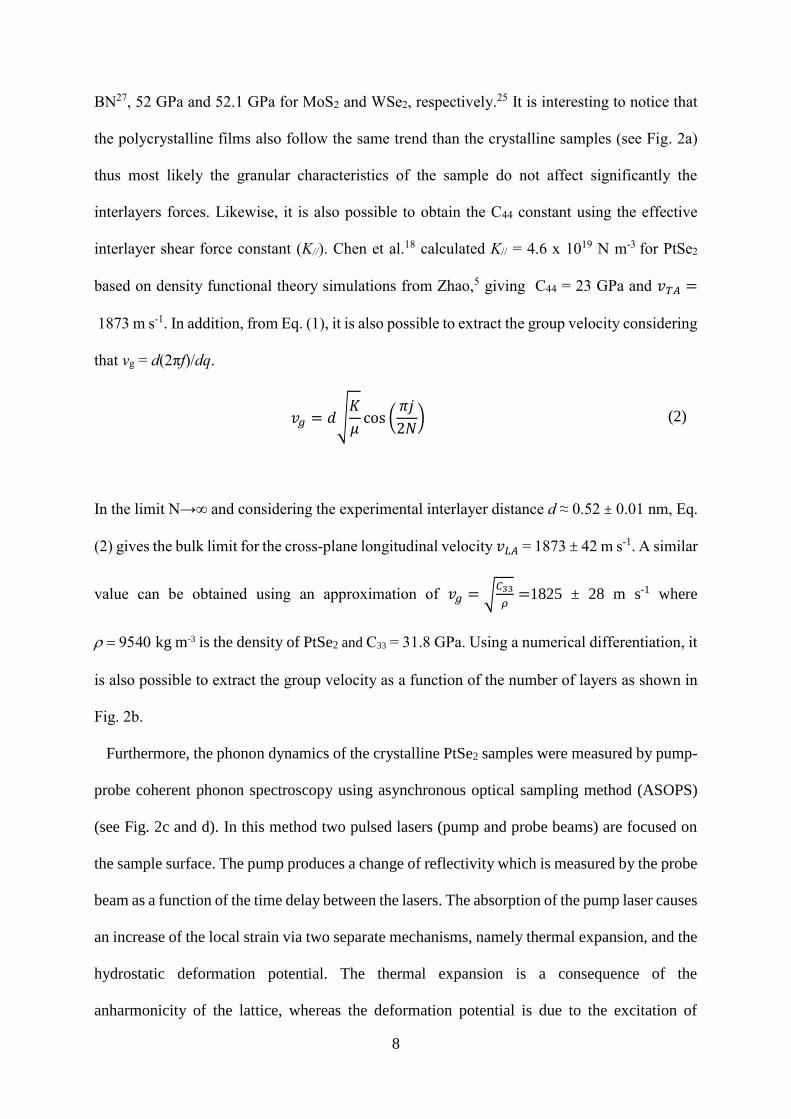
8
BN27, 52 GPa and 52.1 GPa for MoS2 and WSe2, respectively.25 It is interesting to notice that
the polycrystalline films also follow the same trend than the crystalline samples (see Fig. 2a)
thus most likely the granular characteristics of the sample do not affect significantly the
interlayers forces. Likewise, it is also possible to obtain the C44 constant using the effective
interlayer shear force constant (K//). Chen et al.18 calculated K// = 4.6 x 10¹⁹ N m-3 for PtSe2
based on density functional theory simulations from Zhao,5 giving C44 = 23 GPa and 𝑣𝑇𝐴 =
1873 m s-1. In addition, from Eq. (1), it is also possible to extract the group velocity considering
that vg = d(2πf)/dq.
𝑣𝑔 = 𝑑√𝐾
𝜇cos(
𝜋𝑗
2𝑁) (2)
In the limit N→∞ and considering the experimental interlayer distance d ≈ 0.52 ± 0.01 nm, Eq.
(2) gives the bulk limit for the cross-plane longitudinal velocity 𝑣𝐿𝐴 = 1873 ± 42 m s-1. A similar
value can be obtained using an approximation of 𝑣𝑔 = √𝐶33
𝜌=1825 ± 28 m s-1 where
kg m-3 is the density of PtSe2 and C33 = 31.8 GPa. Using a numerical differentiation, it
is also possible to extract the group velocity as a function of the number of layers as shown in
Fig. 2b.
Furthermore, the phonon dynamics of the crystalline PtSe2 samples were measured by pump-
probe coherent phonon spectroscopy using asynchronous optical sampling method (ASOPS)
(see Fig. 2c and d). In this method two pulsed lasers (pump and probe beams) are focused on
the sample surface. The pump produces a change of reflectivity which is measured by the probe
beam as a function of the time delay between the lasers. The absorption of the pump laser causes
an increase of the local strain via two separate mechanisms, namely thermal expansion, and the
hydrostatic deformation potential. The thermal expansion is a consequence of the
anharmonicity of the lattice, whereas the deformation potential is due to the excitation of

9
electrons into binding orbitals. Both mechanisms periodically change the effective volume of
the material, which in turn modulates the optical properties of the film that are probed by the
second laser.
In this experiment, we used 2 fs Ti:sapphire lasers with a repetition rate of ∼ 1 GHz stabilized
via an electronic feedback loop to achieve a small repetition rate difference of 2 kHz. The rate
difference produces a time delay between the pump and probe pulses without the need of
mechanical delay stage.28,29 The delay between the pump pulses is kept at 1 ns, while the pump
and probe pulses coincide every 500 ms. The measurements were done at a fixed central
wavelength of λ = 790 nm for the pump (~1 mW) and the probe (~0.15 mW) beams, collinearly
focused to a ~ 1 μm-diameter spot on the sample surface. Figure 2c shows the typical
modulation of the reflectivity (ΔR/R) as a function of the time delay (black open circles) and
the corresponding best model fit in a 5 ML PtSe2 single crystalline film. The change of
reflectivity includes the effects of a fast and slow electronic relaxation processes as well as the
dynamics of the generated phonons. The time traces are fitted to damped harmonic oscillator
of the form:18
∆𝑅/𝑅 =∑𝐴𝑖exp (−𝑡
𝜏𝑖)
2
𝑖=1
+∑𝐵𝑗exp (−𝑡
𝜏𝑗) sin(2𝜋𝑓𝑗𝑡 + 𝜙𝑗)
2
𝑗=1
(3)
where t is the time delay between the pump and the probe lasers, A and B are the amplitudes,
are the decay times, f the phonon frequency and is a phase delay. The first term of Eq. (3)
represents the fast and slow relaxation processes of the excited carriers. The second term
describes the damped phonon oscillations. The Fast Fourier transforms (FFT) of the time-
domain data for of all measured samples are displayed in the Supplementary.
Figure 2d shows the measured decay time of LBM as a function of the number of layers
(yellow dots) and the calculated phonon decay due to boundary scattering contribution based
on the model proposed by Ziman.30 This model considers the impact of the roughness (η) of the
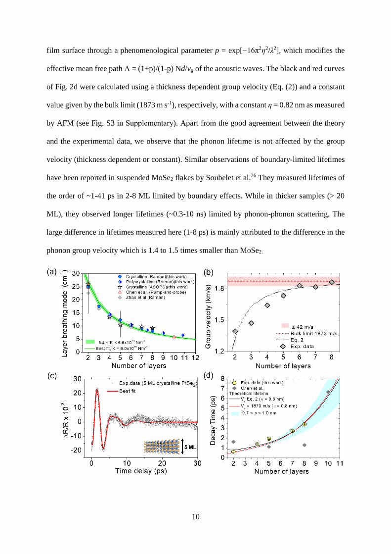
10
film surface through a phenomenological parameter p = exp[−16π2η2/λ2], which modifies the
effective mean free path Λ = (1+p)/(1-p) Nd/vg of the acoustic waves. The black and red curves
of Fig. 2d were calculated using a thickness dependent group velocity (Eq. (2)) and a constant
value given by the bulk limit (1873 m s-1), respectively, with a constant η = 0.82 nm as measured
by AFM (see Fig. S3 in Supplementary). Apart from the good agreement between the theory
and the experimental data, we observe that the phonon lifetime is not affected by the group
velocity (thickness dependent or constant). Similar observations of boundary-limited lifetimes
have been reported in suspended MoSe2 flakes by Soubelet et al.26 They measured lifetimes of
the order of ~1-41 ps in 2-8 ML limited by boundary effects. While in thicker samples (> 20
ML), they observed longer lifetimes (~0.3-10 ns) limited by phonon-phonon scattering. The
large difference in lifetimes measured here (1-8 ps) is mainly attributed to the difference in the
phonon group velocity which is 1.4 to 1.5 times smaller than MoSe2.
11
Fig. 2 Phonon dynamics in PtSe2. (a) Peak position of the first order breathing mode measured
in crystalline and polycrystalline PtSe2 films using low-frequency Raman spectroscopy and
ASOPS as a function of the number of layers and comparison with other experimental works.
(b) Calculated group velocity as a function of the number of layers. (c) Representative
transmission signal obtained with ASOPS in 5 ML PtSe2 (black open circles) and the best fit
(red line). (d) The extracted phonon decay time (yellow dots) vs the number of layers. The red
and black curves are theoretical predictions of the phonon lifetimes based on the model
proposed by Ziman.30 The region displayed with light blue shows the impact of roughness in
the calculated lifetimes. The grey data points show phonon lifetimes measured by Chen et al.18
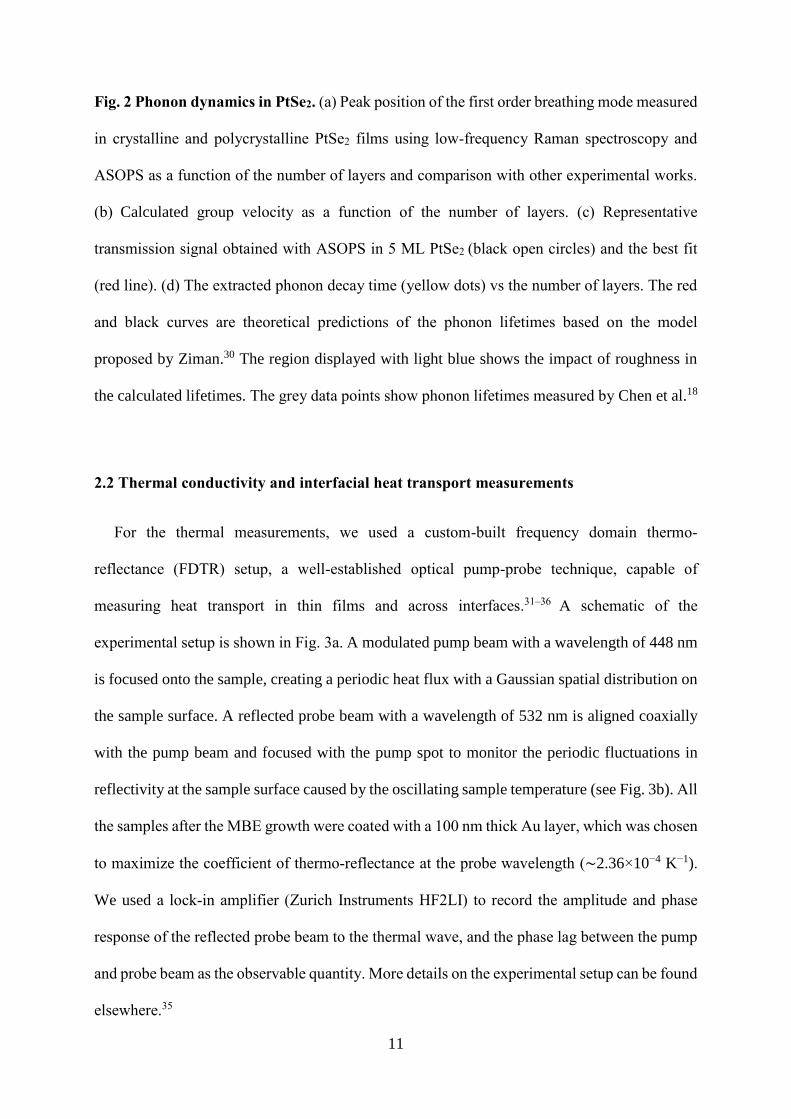
2.2 Thermal conductivity and interfacial heat transport measurements
For the thermal measurements, we used a custom-built frequency domain thermo-
reflectance (FDTR) setup, a well-established optical pump-probe technique, capable of
measuring heat transport in thin films and across interfaces.31–36 A schematic of the
experimental setup is shown in Fig. 3a. A modulated pump beam with a wavelength of 448 nm
is focused onto the sample, creating a periodic heat flux with a Gaussian spatial distribution on
the sample surface. A reflected probe beam with a wavelength of 532 nm is aligned coaxially
with the pump beam and focused with the pump spot to monitor the periodic fluctuations in
reflectivity at the sample surface caused by the oscillating sample temperature (see Fig. 3b). All
the samples after the MBE growth were coated with a 100 nm thick Au layer, which was chosen
to maximize the coefficient of thermo-reflectance at the probe wavelength (∼2.36×10⁻⁴ K−1).
We used a lock-in amplifier (Zurich Instruments HF2LI) to record the amplitude and phase
response of the reflected probe beam to the thermal wave, and the phase lag between the pump
and probe beam as the observable quantity. More details on the experimental setup can be found
elsewhere.35

12
In the present experiments, we obtained frequency-domain measurements by varying the
modulation frequency of the pump beam over a wide range (20 kHz–40 MHz). The cross-plane
thermal conductivity (kz) of the PtSe2 thin films was subsequently extracted by following a
multilayer three-dimensional (3D) heat diffusion model that includes the interface thermal
conductance between the different layers and anisotropic heat transport.31 For each experiment,
we quantified first the sensitivity of the recorded phase signal to different parameters: kz, the
volumetric heat capacity (C), the thermal conductivity anisotropy ratio (kr/kz), and the different
interface thermal conductance’s, in a similar manner to that of Schmidt et al.31 The details about
the measurement sensitivity to different combinations of parameters in the model can be found
in the Supplementary (Fig. S4). In all the experiments we used a high-magnification 50×
objective lens that produced a focused root-mean-square (rms) spot size (1/e2 radius) of
approximately ~1.5 μm. To reduce the uncertainties associated with variations in the laser spot
size between measurements on different films, the spot size was measured for each different
experiment using the knife’s edge method, as shown in the SI (see Fig. S6). All the
measurements were performed under both ambient and vacuum conditions, at room temperature
(Tamb=22°𝐶).
Before the thermal measurements on thin PtSe2 films, we performed FDTR measurements
on a bulk PtSe2 crystal coated with 100 nm of Au in order to extract the anisotropy ratio of the
thermal conductivities. The thermal conductivity of the deposited Au film was first measured
using electrical conductivity and the Wiedemann−Franz law, kAu =195 Wm−1K−1 (see details in
Supplementary, Fig. S7). The volumetric specific heat of Au and PtSe2 were taken from
literature.10,36 This leaves us with three unknowns: the cross-plane and in-plane thermal
conductivity of the bulk PtSe2 crystal and the Au-PtSe2 interface thermal conductance (GAu-
bulk). The in-plane thermal conductivity was expressed in terms of the anisotropic ratio (α) and
the cross-plane thermal conductivity kr = α ·kz.

13
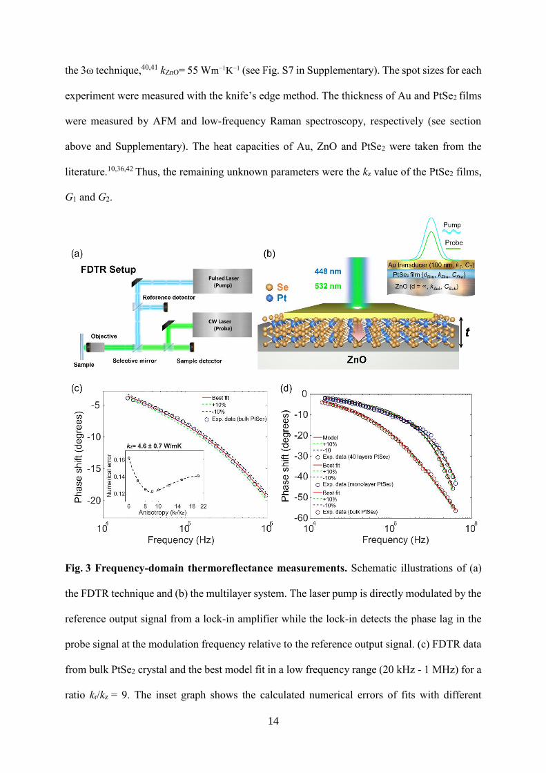
However, from the sensitivity analysis we found that the recorded phase signal has low
sensitivity to GAu-bulk and only at high frequencies while its sensitivity to the anisotropic heat
flow is high in almost the whole frequency range (see Fig. S5 in Supplementary). This allowed
us to extract α directly from the model fit of the experimental data in the low frequency range
(20 kHz–1 MHz) using a nonlinear least-squares routine, which requires an initial guess to
determine the value of the free parameter (kz) (see Fig. 3c). The inset in Fig. 3c shows the
numerical errors of the applied model fits as a function of different anisotropy ratios. The
minimum value of the fitting error, which gives us the best fit of the FDTR data, corresponds
to α = 9, a cross-plane thermal conductivity of 4.6 ± 0.7 Wm−1K−1 and kr ≈ 41.4 Wm-1K-1. The
observed anisotropy ratio between kr and kz in PtSe2 is similar with previous reported values of
other 2D-layered materials, such as InSe (α ~ 10),37 SnSe2 (α ~ 7-8)35,38 and armchair black
phosphorous (α ~ 6-10).39 Our first-principles BTE calculations give kz = 2.84 Wm-1K-1 and kr
= 39.0 Wm-1K-1. kr is in excellent agreement with the measurement, while kz is significantly
overestimated, possibly due to the discrepancy in the equilibrium c lattice parameter mentioned
above. Nevertheless, we can still use DFT and BTE to analyse the phonon contributions to
cross-plane transport in PtSe2 bulk and the effect of finite thickness in thin films, at least
qualitatively.
To study the impact of crystallinity and film thickness on the cross-plane thermal
conductivity of PtSe2 thin films, we performed FDTR measurements in large-area crystalline
and polycrystalline PtSe2 films of different thicknesses (0.6 – 24 nm) on ZnO substrate. The
wedge samples stacks consist of Au/PtSe2/ZnO (see Fig. 3b and Fig. S1 in Supplementary).
Typical examples of the recorded phase signals and the corresponding best model fits for
monolayer and 40 ML crystalline PtSe2 are shown in Fig. 3d. Here, the key parameters for the
model in our multilayer system are: the spot sizes of the pump and probe beams, kz, the film
thickness t, the C of each layer, and the interface thermal conductances (between Au and PtSe2
(G1) and between PtSe2 and ZnO (G2)). The thermal conductivity of ZnO was measured with
14
the 3ω technique,40,41 kZnO= 55 Wm−1K−1 (see Fig. S7 in Supplementary). The spot sizes for each
experiment were measured with the knife’s edge method. The thickness of Au and PtSe2 films
were measured by AFM and low-frequency Raman spectroscopy, respectively (see section
above and Supplementary). The heat capacities of Au, ZnO and PtSe2 were taken from the
literature.10,36,42 Thus, the remaining unknown parameters were the kz value of the PtSe2 films,
G1 and G2.
Fig. 3 Frequency-domain thermoreflectance measurements. Schematic illustrations of (a)
the FDTR technique and (b) the multilayer system. The laser pump is directly modulated by the
reference output signal from a lock-in amplifier while the lock-in detects the phase lag in the
probe signal at the modulation frequency relative to the reference output signal. (c) FDTR data
from bulk PtSe2 crystal and the best model fit in a low frequency range (20 kHz - 1 MHz) for a
ratio kr/kz = 9. The inset graph shows the calculated numerical errors of fits with different
15
anisotropies. (d) Typical FDTR data measured in bulk PtSe2 (red circles), 40 layers (black
circles) and monolayer (blue circles) crystalline PtSe2 films and the corresponding best model
fits in the whole frequency range.
To extract a unique value of kz from a single measurement we followed a fitting approach
similar to that suggested in previous works31,32,35 and supported by our sensitivity analysis (see
Fig. S4 in Supplementary). First, we estimate kz by fitting to experimental data in a low
frequency range (20 kHz - 1 MHz), where the measurement sensitivity to the G1, G2 and heat
capacity of the films is negligible. Then, we fix kz and fit to experimental data in a high
frequency range (1 MHz - 40 MHz) to estimate simultaneously G1 and G2. As initial guess to
determine the value of the free parameters (kz, G1 and G2) we used previous reported values of
similar material systems.43–45 We also verified that the final fit results are not sensitive to the
choice of initial values. The same analysis has been followed to extract kz, G1 and G2 values for
all the PtSe2 films.
It is interesting to note that, in contrast to the bulk case, in FDTR measurements in thin films
the diameter of the laser spot is usually large compared to the thermal diffusion length during
the modulation period of the pump beam. Thus, the heat flow is expected to be mainly one-
dimensional in the cross-plane direction.32 This has been confirmed by our sensitivity analysis,
where we found that the sensitivity of the recorded phase signal to the in-plane transport is
relatively low (see Fig. S4c in Supplementary). Therefore, since anisotropic differences in
thermal conductivities as a function of the film thickness cannot be resolved, for the data
analysis we used the anisotropy ratio extracted from the bulk PtSe2 experiments. The
dependence of the thermal anisotropy with the film thickness has been studied recently in
similar material systems, such as supported InSe37 and SnSe235 films, showing a thickness-
independent α of 10 and 8.4, respectively.

16
Figure 4a displays the extracted kz value of all the PtSe2 thin films as a function of thickness.
In both crystalline (black data points) and polycrystalline films (green data points), we observe
a linear increase of kz with increasing the film thickness starting from 2.4 nm (~4 monolayers)
up to 10 nm and 24 nm, respectively. In polycrystalline films with thicknesses t >12 nm, kz
shows a plateau and a maximum cross-plane thermal conductivity reduction of approximately
35% was observed as compared to the crystalline samples. This result highlights the strong
impact of crystallinity on kz and suggests that depending on the film crystallinity phonons with
different mean free paths (MFPs) contribute to the cross-plane thermal conductivity. In
crystalline PtSe2 films, heat is propagating through coherent vibrations (phonon modes) that
travel distances at least 24 nm (~40 monolayers) while in polycrystalline samples, they start to
decay above 12 nm (~20 monolayers). This behavior most likely is attributed to the enhanced
phonon scattering due to the presence of a high density of defective grain boundaries randomly
oriented in the polycrystalline film.
In Fig. 4a, we also show the kz obtained from first-principles DFT-BTE calculations, both,
for bulk PtSe2 and thickness dependent values as two different sets of data. The first set accounts
solely for the finite thickness of the film and gives an overall much larger thermal conductivity
than the measured one at the corresponding thickness (red data points). The overestimation of
the calculated thermal conductivity for the whole thickness range can be related to the
underestimation of the c-axis compared with the experimental data and the assumption of a
perfect single-crystal structure of the films. In addition, G1 and G2 were not taken into account
in the DFT calculations, which further explains the overestimated values in the calculated
thickness dependence of kz. However, we observe that the trend of thickness-dependent of the
thermal conductivity is preserved. Finally, correcting the BTE calculation for the observed
thickness-dependent reduction of sound velocity provides better agreement between theory and
experiments over the whole range of thickness considered (yellow-black diamonds).

17
The observed linear dependence of kz from 4 monolayers up to a certain thickness in both
sets of samples is consistent with ballistic heat conduction processes, as has been shown in
previous works, where the thermal conductivity increased linearly with the characteristic length
of the system.43,46,47 However, in few-layer crystalline PtSe2 films (t < 2-3 nm), we observe a
deviation from the linear thickness-dependence of kz (see Fig. 4a, black spheres). Since
interfaces might dominate cross-plane heat transport in very thin films, the apparent deviation
might be attributed to variations in the total thermal resistance per unit area, Rtot, of the film
(see calculations below), which can be written as the sum of the combined interface thermal
resistance, Rint= 1/G1 + 1/G2, and volumetric cross-plane thermal resistance, RPtSe2= t/kz.43,48
Note that this expression is not valid in very thin films and G1, G2 should be treated as one
diffusive interface instead of two discrete ones.43,48 Another possible explanation for this
deviation is the semiconductor-to-semimetal evolution of PtSe2 films after 4 monolayers (~ 2
nm),49 which might result in an additional contribution of the electron thermal conductivity to
kz and/or lower contact resistivity between PtSe2 and Au.12
To quantify the impact of cross-plane ballistic phonon transport on the total thermal
resistance of multilayer PtSe2 films, we plotted the total thermal resistance, Rtot=RPtSe2+Rint,
versus film thickness (Fig. 3b). We observe that in crystalline PtSe2 Rtot remains almost constant
in the entire thickness range (see black spheres), with values approximately of 28 ± 10 m2KGW-
1, while in polycrystalline samples (see green spheres) Rtot is constant only up to 12 nm and then
starts to increase up to 75 ± 10 m2KGW-1. The large contribution of the volumetric resistance
component, RPtSe2 to Rtot and the thickness-independent Rtot in crystalline films indicate ballistic
phonon transport along the c-axis of the films, as has been previously observed in few-layer-
graphene and single crystal MoS2 flakes that showed a thickness-independent Rtot for film
thicknesses between 0.4 - 4 nm48 and 20 - 40 nm,43 respectively. The increased values of Rtot in
polycrystalline films after 12 nm indicate a transition from ballistic to diffusive transport regime
most likely due to phonon grain boundary scattering. For comparison, in Fig. 4b we plot our

18
calculated Rtot (black and green spheres) with previous total cross-plane thermal resistance
measurements on different 2D materials, where similar interfacial contributions from bottom
(2D material/substrate) and top (metal/2D material) interfaces were taken into account.43,48 Our
values are in line with these estimations and suggest that in sufficiently thin films, phonons
(especially long-wavelength phonons) can directly propagate between the metal and substrate
without being strongly scattered by interfaces.
Fig. 4 Thermal conductivity and interfacial heat transport measurements. (a) Cross-plane
thermal conductivity kz of crystalline (black spheres) and polycrystalline (green spheres) PtSe2
films versus film thickness t. The uncertainty of the estimated kz was calculated based on error
propagation for the input parameters. The blue and red lines in (a) display the bulk cross-plane
thermal conductivity values obtained by FDTR and DFT calculations, respectively. The black
and green curved are a guide for the eye. (b) Total thermal resistance, Rtotal = Rint + RPtSe2, of
crystalline (black spheres) and polycrystalline (green spheres) PtSe2 thin films, plotted versus
film thickness t. The uncertainty region is displayed as a grey rectangle. The total cross-plane
thermal resistance measurements of Au/graphene/SiO248 (red diamonds) and Al/MoS2/SiO2
43
(purple triangles) interfaces are also reported.
To further confirm the robustness of our approach to measure the intrinsic cross-plane
thermal conductivity of thin films, we performed Raman thermometry measurements in few
layers crystalline PtSe2 films (2, 3 and 4 layers of PtSe2, see Fig. S8 in Supplementary), where
19
we found kz values in good agreement with the FDTR results (see Table S1 in Supplementary).
The agreement between Raman and FDTR experiments further supports our Rtot calculations
and show that it is possible to quantify the interfacial thermal contributions in a multilayer
structure from a single set of FDTR measurements despite the low phase sensitivity to G1 and
G2. Note that in Raman thermometry measurements we have only the contribution of R2 to the
total thermal resistance.
As discussed above, to calculate the frequency response of the surface temperature to the
pump beam we followed a multilayer 3D heat diffusion model that considers anisotropic
transport.[33] To validate if a diffusive model is suitable, we estimate the room temperature
phonon MFP in the cross-plane direction (Λz) using a simplified expression from the kinetic
theory, kz ∼ (1/3)CυsΛz, where υs is the averaged sound velocity of cross-plane acoustic modes.
For PtSe2 we used C ∼ 1.78 MJm-3K-1 50 while kz and υs were determined experimentally (kz ∼
4.6 Wm−1K−1, υs ∼√1
3(
1
𝑣𝐿𝐴3 +
2
𝑣𝑇𝐴3 )
3) through our FDTR experiments and ASOPS measurements
described above. From this estimation, we found Λz ∼ 5 nm, which corresponds to a thickness
of approximately 10 layers. However, our FDTR experimental data suggest that in crystalline
PtSe2 films phonons with Λz> 24 nm substantially contribute to the thermal conductivity (about
37% of the bulk value, from our BTE-DFT calculations) while in polycrystalline films grain
boundary scattering reduces this value to approximately 12 nm (see Fig. 4a). This is in close
agreement with our DFT calculations that show that phonons with MFP larger than 15 nm
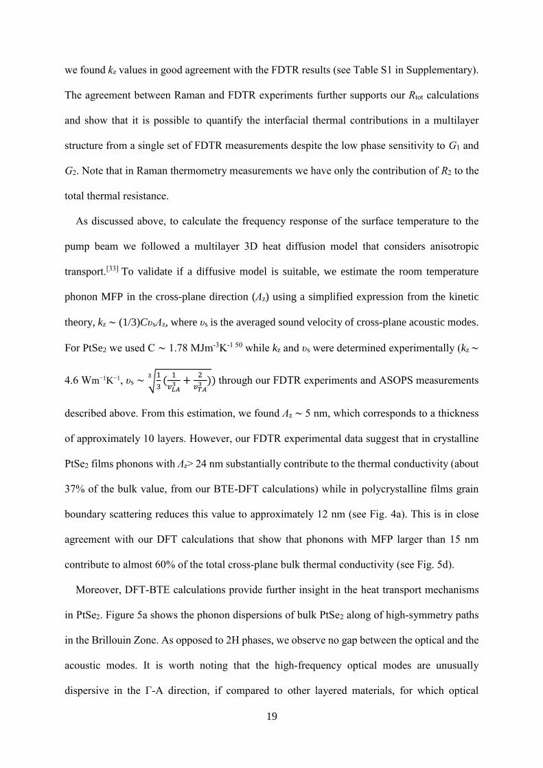
contribute to almost 60% of the total cross-plane bulk thermal conductivity (see Fig. 5d).
Moreover, DFT-BTE calculations provide further insight in the heat transport mechanisms
in PtSe2. Figure 5a shows the phonon dispersions of bulk PtSe2 along of high-symmetry paths
in the Brillouin Zone. As opposed to 2H phases, we observe no gap between the optical and the
acoustic modes. It is worth noting that the high-frequency optical modes are unusually
dispersive in the Γ-A direction, if compared to other layered materials, for which optical
20
phonons dispersions are usually flat.51 This can be seen in Fig. 5b which displays the group
velocities along the same k-point paths. Figure 5b also shows that the speed of sound in the Γ-
A direction, averaged over the three acoustic branches, is 1930 m s-1 (vLA =2120 m s-1). In
addition, in Fig. 5c we show that the MFPs in the cross-plane direction of the acoustic modes
may be as high as 200 nm. Remarkably, there is a large number of optical modes with MFPs
between 1 to 10 nm. This leads to a significant contribution of the optical modes to the thermal
conductivity of bulk and films of PtSe2, as shown in Fig. 5d and Fig. S10 in the SI.
Fig. 5 First-principles DFT calculations. (a) Phonon dispersion relations and (b) group
velocity of bulk PtSe2 along high-symmetry directions in the Brillouin zone. (c) Calculated bulk
phonon mean free as a function of frequency. (d) Normalized thermal conductivity
accumulation (kacc) as a function of the phonon frequency (red curve) and MFP (blue curve) for
bulk PtSe2.

21
In particular, Fig. 5d shows the normalized cumulative thermal conductivity as a function of
frequency (red axis) and phonon mean free path (black axis) for bulk PtSe2. We observe a quite
narrow MFP distribution (1-200 nm) but much longer than the rough estimation from the kinetic
theory ~5 nm. This discrepancy it is well known and comes from the fact that each phonon
contributes in a different manner to the thermal conductivity.43,52–54 An averaged value can be
very misleading and underestimate the real contribution of the phonon MFP to the total thermal
conductivity. Finally, it is interesting to note the rather large contribution (~ 30%) of low-
frequency phonons (< 1 THz) to the total thermal conductivity. These phonons modes are
sensitive to the introduction of additional periodicity and their dispersion relation can be easily
tuned through nanofabrication.55,56 This opens the possibility of exploring alternative ways of
tuning thermal conduction through phonon engineering in two-dimensional materials.
3. Conclusion
In conclusion, we have studied phonon dynamic properties and heat transport in MBE-grown
crystalline and polycrystalline PtSe2 thin films of varying thickness (0.6 – 24) nm using a
combination of characterization techniques, i.e., FDTR, low-frequency Raman and pump-probe
coherent phonon spectroscopies, and state-of-the-art DFT calculations. Our work demonstrates
the ability to quantify the influence of thickness and crystallinity on the cross-plane heat
propagation in thin layered PtSe2 films, showing an almost 35% reduction in the thermal
conductivity of polycrystalline films with thickness larger than 12 nm in comparison with
crystalline films of the same thickness. Moreover, from the phonon dynamic study in crystalline
PtSe2 we extract an out-of-plane elastic constant C33 =31.8 GPa and a layer-dependent group
velocity ranging from 1340 m s-1 in bilayer PtSe2 to 1873 m s-1 in 8 layers of PtSe2. Last, we
showed that acoustic phonons in PtSe2 thin films, which are the main carriers of heat in
semiconductors, have extraordinarily short lifetimes in the order of picoseconds. Our results
provide a new insight into the heat transport and phonon dynamics in 2D materials at the

22
nanoscale, with potential implications for future design of 2D-based devices for energy
harvesting and effective heat dissipation in thermoelectric and optoelectronic devices.
Methods
MBE growth: Pt and Se were respectively evaporated thanks to an e-gun evaporator and a
standard effusion cell. The Pt deposition rate was set to 0.75 Åmin-1 and monitored in real time
by a quartz crystal microbalance. The pressure of Se at the sample position was measured with
a retractable ionization gauge and set to 1.0×10⁻⁶ mbar, which corresponds to a Se:Pt flux ratio
of about 15. The MBE reactor is connected under UHV to a magnetron sputtering chamber with
a Pt target. The Pt deposition rate was set to 4.7 Åmin-1 thanks to a retractable quartz crystal
microbalance, the DC magnetron power was 1 W and the argon pressure 1.2×10⁻² mbar. The
ZnO(0001) substrates (CrysTec GmbH) were first etched for 30 s with an HCl 1.8% solution
and rinsed with deionized water. This chemical treatment was followed by annealing for 1h at
900°C in O2 atmosphere, then annealing in UHV for 5 min at ~800°C.
XRD: Grazing-incidence x-ray diffraction measurements were performed with a SmartLab
Rigaku diffractometer. The source is a rotating anode beam tube (Cu Kα = 1.54 Å) operating at
45 kV and 200 mA. The diffractometer is equipped with a parabolic multilayer mirror and in-
plane collimators of 0.5° on both source and detector sides defining the angular resolution. A
Kβ filter on the detector side eliminates parasitic radiations.
DFT: We computed the lattice thermal conductivity of 1T (octahedral) PtSe2 by density
functional theory (DFT) and the Boltzmann transport equation (BTE). In the DFT calculations,
we used a van der Waals density functional with consistent exchange (vdW-DF-CX) that
reliably predicts the structural and vibrational properties of several 2D materials, including
transition metal dichalcogenides.57,58 Valence Kohn-Sham wavefunctions are expanded on
plane-waves basis set with a cutoff of 40 Ry, and projector augmented pseudopotentials are
23
used to model screened nuclei.59 A uniform 8x8x6 mesh of k-points was used to integrate the
first Brillouin Zone. Phonon dispersion relations were computed by density functional
perturbation theory interpolating a uniform 4x4x3 q-point mesh.60,61
BTE: Second-order and third-order force constants for the thermal conductivity calculations
were computed by fitting the forces of 80 configurations of the 4x4x3 PtSe2 supercell, in which
the atoms are randomly displaced with a standard deviation of 0.01 Å using the hiPhive code.62
Second-order and third-order force constants were cut off at 6.9 Å and 5.13 Å, respectively.
Fitting employed recursive feature elimination with a limit of 300 features (out of 961). The fit
gives a root mean square error on the forces of 0.0044 eV/A with R2 = 0.999. The solution of
the linearized phonon BTE was computed by directly inverting the scattering tensor on a
21x21x17 mesh of q-points, as implemented in kALDo.63 The effect of the finite thickness of
the samples is taken into account by including the boundary conditions in the scattering term
as proposed by Maassen and Lundstrom.64
Data availability
All relevant data are available from the corresponding author on request.
Acknowledgements
This work has been supported by the Severo Ochoa program, the Spanish Research Agency
(AEI, grant no. SEV-2017-0706) and the CERCA Programme/Generalitat de Catalunya. The
authors acknowledge support from Spanish MICINN project SIP (PGC2018-101743-B-I00),
and the EU project NANOPOLY (GA 289061). The LANEF framework (ANR-10-LABX-51-
01) is acknowledged for its support with mutualized infrastructure. P.X. acknowledges support
by Ph.D. fellowship from the EU Marie Sklodowska-Curie COFUND PREBIST (Grant
Agreement 754558). A.E.S. acknowledges support by the H2020-MSCA-IF project
THERMIC-GA No. 101029727.
Author Contributions
24
A.E.S. and E.C.A. conceived the project. A.E.S and E.C.A. built the FDTR setup, performed
the thermal measurements and data analysis. A.E.S. performed the AFM measurements. E.C.A.
and P.X. performed the Raman measurements. E.C.A. and A.G. performed the ASOPS
measurements and analysis. F. B., A.M., C.V, H.B. and M. J. fabricated the MBE samples and
performed the XRD measurements. P.X., M.S., A.E.S. and E.C.A. performed the TEM
measurements and the structural analysis. D. D. and Z.C. performed the DFT calculations and
provide support to the theoretical analysis. All authors reviewed and edited the manuscript and
have given approval to the final version of the manuscript. The manuscript was written by
A.E.S. and E.C.A. A.E.S. and P.X. contributed equally.
Competing interests
The authors declare no competing interests.
Additional information
Supplementary information. The online version contains supplementary material available.
Reflection high energy electron and X-ray diffraction measurements, FDTR sensitivity
analysis, spot size measurements, AFM measurements, three omega measurements, Raman
thermometry measurements, ASOPS measurements, DFT calculations.
References
1. Ferrari, A. C. et al. Science and technology roadmap for graphene, related two-
dimensional crystals, and hybrid systems. Nanoscale 7, 4598–4810 (2015).
2. Jariwala, D. et al. Gate-tunable carbon nanotube-MoS2 heterojunction p-n diode. Proc.
Natl. Acad. Sci. 110, 18076–18080 (2013).
3. Massicotte, M. et al. Picosecond photoresponse in van der Waals heterostructures. Nat.
Nanotechnol. 11, 42–46 (2016).
4. Chhowalla, M., Jena, D. & Zhang, H. Two-dimensional semiconductors for transistors.
Nat. Rev. Mater. 1, 16052 (2016).
25
5. Zhao, Y. et al. High-Electron-Mobility and Air-Stable 2D Layered PtSe2 FETs. Adv.
Mater. 29, 1604230 (2017).
6. Deng, Y. et al. Black Phosphorus–Monolayer MoS2 van der Waals Heterojunction p–n
Diode. ACS Nano 8, 8292–8299 (2014).
7. Yu, X. et al. Atomically thin noble metal dichalcogenide: a broadband mid-infrared
semiconductor. Nat. Commun. 9, 1545 (2018).
8. Liu, Y., Zhang, S., He, J., Wang, Z. M. & Liu, Z. Recent Progress in the Fabrication,
Properties, and Devices of Heterostructures Based on 2D Materials. Nano-Micro Lett.
11, 13 (2019).
9. Li, D. et al. Recent Progress of Two-Dimensional Thermoelectric Materials. Nano-
Micro Lett. 12, 36 (2020).
10. Gong, Y. et al. Two-Dimensional Platinum Diselenide: Synthesis, Emerging
Applications, and Future Challenges. Nano-Micro Lett. 12, 174 (2020).
11. Bonell, F. et al. High carrier mobility in single-crystal PtSe 2 grown by molecular
beam epitaxy on ZnO(0001). 2D Mater. (2021) doi:10.1088/2053-1583/ac37aa.
12. Yim, C. et al. Electrical devices from top-down structured platinum diselenide films.
npj 2D Mater. Appl. 2, 5 (2018).
13. Zhang, W., Qin, J., Huang, Z. & Zhang, W. The mechanism of layer number and strain
dependent bandgap of 2D crystal PtSe2. J. Appl. Phys. 122, 205701 (2017).
14. Wang, Y. et al. Monolayer PtSe2, a New Semiconducting Transition-Metal-
Dichalcogenide, Epitaxially Grown by Direct Selenization of Pt. Nano Lett. 15, 4013–
4018 (2015).
15. Moon, H. et al. Strong Thermopower Enhancement and Tunable Power Factor via
Semimetal to Semiconductor Transition in a Transition-Metal Dichalcogenide. ACS
Nano 13, 13317–13324 (2019).
16. Guo, S.-D. Biaxial strain tuned thermoelectric properties in monolayer PtSe2. J. Mater.
Chem. C 4, 9366–9374 (2016).
17. Yin, S. et al. Thermal Conductivity of Few-Layer PtS 2 and PtSe 2 Obtained from
Optothermal Raman Spectroscopy. J. Phys. Chem. C 125, 16129–16135 (2021).
18. Chen, X. et al. Direct observation of interlayer coherent acoustic phonon dynamics in
bilayer and few-layer PtSe 2. Photonics Res. 7, 1416 (2019).
19. Zhang, K. et al. Experimental evidence for type-II Dirac semimetal in PtSe2. Phys.
Rev. B 96, 125102 (2017).
20. Cooper, V. R. Van der Waals density functional: An appropriate exchange functional.
26
Phys. Rev. B 81, 161104 (2010).
21. Terentjev, A. V., Constantin, L. A. & Pitarke, J. M. Dispersion-corrected PBEsol
exchange-correlation functional. Phys. Rev. B 98, 214108 (2018).
22. O’Brien, M. et al. Raman characterization of platinum diselenide thin films. 2D Mater.
3, 021004 (2016).
23. Luo, N. S., Ruggerone, P. & Toennies, J. P. Theory of surface vibrations in epitaxial
thin films. Phys. Rev. B 54, 5051–5063 (1996).
24. Carpinteri, A. Structural Mechanics. (CRC Press, 2014). doi:10.1201/9781315274454.
25. Zhao, Y. et al. Interlayer breathing and shear modes in few-trilayer MoS2 and WSe2.
Nano Lett. 13, 1007–15 (2013).
26. Soubelet, P. et al. The lifetime of interlayer breathing modes of few-layer 2H-MoSe 2
membranes. Nanoscale 11, 10446–10453 (2019).
27. Jiménez-Riobóo, R. J. et al. In- and out-of-plane longitudinal acoustic-wave velocities
and elastic moduli in h-BN from Brillouin scattering measurements. Appl. Phys. Lett.
112, 051905 (2018).
28. Elzinga, P. A., Lytle, F. E., Jian, Y., King, G. B. & Laurendeau, N. M. Pump/Probe
Spectroscopy by Asynchronous Optical Sampling. Appl. Spectrosc. 41, 2–4 (1987).
29. Bartels, A. et al. Ultrafast time-domain spectroscopy based on high-speed
asynchronous optical sampling. Rev. Sci. Instrum. 78, 35107 (2007).
30. Ziman, J. M. Electrons and Phonons. The theory of transport phenomena in solids.
(Oxford University Press, USA, 1960).
31. Schmidt, A. J., Cheaito, R. & Chiesa, M. A frequency-domain thermoreflectance
method for the characterization of thermal properties. Rev. Sci. Instrum. 80, 094901
(2009).
32. Schmidt, A. J., Chen, X. & Chen, G. Pulse accumulation, radial heat conduction, and
anisotropic thermal conductivity in pump-probe transient thermoreflectance. Rev. Sci.
Instrum. 79, 114902 (2008).
33. El Sachat, A., Alzina, F., Sotomayor Torres, C. M. & Chavez-Angel, E. Heat Transport
Control and Thermal Characterization of Low-Dimensional Materials: A Review.
Nanomaterials 11, 175 (2021).
34. Sandell, S. et al. Thermoreflectance techniques and Raman thermometry for thermal
property characterization of nanostructures. J. Appl. Phys. 128, 131101 (2020).
35. Xiao, P. et al. Anisotropic Thermal Conductivity of Crystalline Layered SnSe 2. Nano
Lett. 21, 9172–9179 (2021).

27
36. Sandell, S. et al. Enhancement of Thermal Boundary Conductance of Metal–Polymer
System. Nanomaterials 10, 670 (2020).
37. Rai, A., Sangwan, V. K., Gish, J. T., Hersam, M. C. & Cahill, D. G. Anisotropic
thermal conductivity of layered indium selenide. Appl. Phys. Lett. 118, 73101 (2021).
38. Wang, H., Gao, Y. & Liu, G. Anisotropic phonon transport and lattice thermal
conductivities in tin dichalcogenides SnS2 and SnSe2. RSC Adv. 7, 8098–8105 (2017).
39. Jang, H., Wood, J. D., Ryder, C. R., Hersam, M. C. & Cahill, D. G. Anisotropic
Thermal Conductivity of Exfoliated Black Phosphorus. Adv. Mater. 27, 8017–8022
(2015).
40. Cahill, D. G. Thermal conductivity measurement from 30 to 750 K: the 3ω method.
Rev. Sci. Instrum. 61, 802 (1990).
41. Cahill, D. G. Erratum: “Thermal conductivity measurement from 30 to 750 K: The 3ω
method” [Rev. Sci. Instrum. 61, 802 (1990)]. Rev. Sci. Instrum. 73, 3701 (2002).
42. Serrano, J. et al. Heat capacity of ZnO: Isotope effects. Phys. Rev. B 73, 94303 (2006).
43. Sood, A. et al. Quasi-Ballistic Thermal Transport Across MoS2 Thin Films. Nano Lett.
19, 2434–2442 (2019).
44. Subramanyan, H., Kim, K., Lu, T., Zhou, J. & Liu, J. On the importance of using exact
full phonon dispersions for predicting interfacial thermal conductance of layered
materials using diffuse mismatch model. AIP Adv. 9, 115116 (2019).
45. Liu, X., Zhang, G. & Zhang, Y.-W. Thermal conduction across the one-dimensional
interface between a MoS2 monolayer and metal electrode. Nano Res. 9, 2372–2383
(2016).
46. Hsiao, T.-K. et al. Observation of room-temperature ballistic thermal conduction
persisting over 8.3 µm in SiGe nanowires. Nat. Nanotechnol. 8, 534–538 (2013).
47. Vakulov, D. et al. Ballistic Phonons in Ultrathin Nanowires. Nano Lett. 20, 2703–2709
(2020).
48. Koh, Y. K., Bae, M.-H., Cahill, D. G. & Pop, E. Heat Conduction across Monolayer
and Few-Layer Graphenes. Nano Lett. 10, 4363–4368 (2010).
49. Ansari, L. et al. Quantum confinement-induced semimetal-to-semiconductor evolution
in large-area ultra-thin PtSe2 films grown at 400 °C. npj 2D Mater. Appl. 3, 33 (2019).
50. Maregedze, C. N. Numerical simulation of structural electronic, optical and thermal
properties of platinium dichalcogenides. (University of Witwatersrand, 2019).
51. Mortazavi, B. et al. Exploring phononic properties of two-dimensional materials using
machine learning interatomic potentials. Appl. Mater. Today 20, 100685 (2020).
28
52. Cuffe, J. et al. Reconstructing phonon mean-free-path contributions to thermal
conductivity using nanoscale membranes. Phys. Rev. B 91, 245423 (2015).
53. Henry, A. S. & Chen, G. Spectral Phonon Transport Properties of Silicon Based on
Molecular Dynamics Simulations and Lattice Dynamic. J. Comput. Theor. Nanosci. 5,
141–152 (2008).
54. Esfarjani, K., Chen, G. & Stokes, H. Heat transport in silicon from first-principles
calculations. Phys. Rev. B 84, (2011).
55. Graczykowski, B. et al. Phonon dispersion in hypersonic two-dimensional phononic
crystal membranes. Phys. Rev. B 91, 75414 (2015).
56. Sledzinska, M. et al. 2D Phononic Crystals: Progress and Prospects in Hypersound and
Thermal Transport Engineering. Adv. Funct. Mater. 30, 1904434 (2019).
57. Berland, K. & Hyldgaard, P. Exchange functional that tests the robustness of the
plasmon description of the van der Waals density functional. Phys. Rev. B 89, 035412
(2014).
58. Lindroth, D. O. & Erhart, P. Thermal transport in van der Waals solids from first-
principles calculations. Phys. Rev. B 94, 115205 (2016).
59. Blöchl, P. E. Projector augmented-wave method. Phys. Rev. B 50, 17953–17979
(1994).
60. Baroni, S., de Gironcoli, S., Dal Corso, A. & Giannozzi, P. Phonons and related crystal
properties from density-functional perturbation theory. Rev. Mod. Phys. 73, 515–562
(2001).
61. Giannozzi, P. et al. Advanced capabilities for materials modelling with Quantum
ESPRESSO. J. Phys. Condens. Matter 29, 465901 (2017).
62. Eriksson, F., Fransson, E. & Erhart, P. The Hiphive Package for the Extraction of
High‐Order Force Constants by Machine Learning. Adv. Theory Simulations 2,
1800184 (2019).
63. Barbalinardo, G., Chen, Z., Lundgren, N. W. & Donadio, D. Efficient anharmonic
lattice dynamics calculations of thermal transport in crystalline and disordered solids. J.
Appl. Phys. 128, 135104 (2020).
64. Maassen, J. & Lundstrom, M. Steady-state heat transport: Ballistic-to-diffusive with
Fourier’s law. J. Appl. Phys. 117, 035104 (2015).

29
Supplementary Information
Phonon dynamics and thermal conductivity of PtSe2 thin
films: Impact of crystallinity and film thickness on heat
dissipation
Alexandros El Sachat*,1, Peng Xiao1,2, Davide Donadio3,4, Frédéric Bonell5, Marianna
Sledzinska1, Alain Marty5, Céline Vergnaud5, Hervé Boukari5, Matthieu Jamet5, Guillermo
Arregui1, Zekun Chen3,4, Francesc Alzina1, Clivia M. Sotomayor Torres1,6, Emigdio Chavez-
Angel*,1
1 Catalan Institute of Nanoscience and Nanotechnology (ICN2), CSIC and BIST, Campus
UAB, Bellaterra, 08193 Barcelona, Spain
2 Departamento de Física, Universidad Autónoma de Barcelona, Bellaterra, 08193 Barcelona,
Spain
3 Department of Chemistry, University of California, Davis, California 95616, United States
4 Ikerbasque, Basque Foundation for Science, E-48011 Bilbao, Spain
5 Université Grenoble Alpes, CNRS, CEA, Grenoble INP, IRIG-Spintec, 38054 Grenoble
6 ICREA, Passeig Lluis Companys 23, 08010 Barcelona, Spain
*Corresponding authors: [email protected], [email protected]

30
1. Reflection high energy electron diffraction, X-ray diffraction and atomic
force microscopy measurements
Supplementary Figure S1. Reflection high energy electron diffraction (RHEED)
measurements and the final structure of the PtSe2 wedge sample. (a) and (b) RHEED
patterns of 4 ML PtSe2 grown by co-evaporation along two different azimuths respectively. (c)
RHEED pattern of the polycrystalline PtSe2 film. Only one azimuth is shown since it is
isotropic. (d) Schematic drawing in cross-section of the final structure.
31
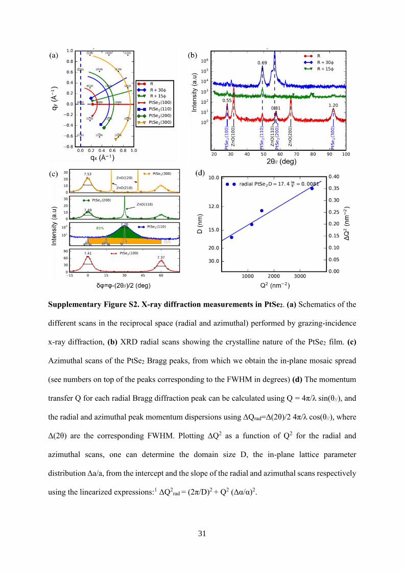
Supplementary Figure S2. X-ray diffraction measurements in PtSe2. (a) Schematics of the
different scans in the reciprocal space (radial and azimuthal) performed by grazing-incidence
x-ray diffraction, (b) XRD radial scans showing the crystalline nature of the PtSe2 film. (c)
Azimuthal scans of the PtSe2 Bragg peaks, from which we obtain the in-plane mosaic spread
(see numbers on top of the peaks corresponding to the FWHM in degrees) (d) The momentum
transfer Q for each radial Bragg diffraction peak can be calculated using Q = 4π/λ sin(θ//), and
the radial and azimuthal peak momentum dispersions using ΔQrad=Δ(2θ)/2 4π/λ cos(θ//), where
Δ(2θ) are the corresponding FWHM. Plotting ΔQ2 as a function of Q2 for the radial and
azimuthal scans, one can determine the domain size D, the in-plane lattice parameter
distribution Δa/a, from the intercept and the slope of the radial and azimuthal scans respectively
using the linearized expressions:1 ΔQ2rad = (2π/D)2 + Q2 (Δα/α)2.

32
Supplementary Figure S3. AFM measurements. (a) Histogram of the height distribution
(surface roughness) measured by AFM for crystalline PtSe2. The root mean square roughness
(RMS), η, is 0.82 nm. The inset shows an AFM image of the crystalline PtSe2 wedge sample.
(b) AFM topography profile of the deposited Au transducer on ZnO substrate taken from the
black dashed line depicted in the AFM image (inset in (b)).
2. FDTR sensitivity analysis
We quantify the phase sensitivity to multiple thermal properties in a similar manner to that of
Schmidt et al.2 The calculated phase sensitivity (-Vin/Vout) to multiple parameters (kz, Cv,
anisotropy, G1 and G2) as a function of thickness and modulation frequency for the case of
Au/PtSe2/ZnO stacks is shown in Fig. S4(a-e). For the sensitivity analysis, we fit the
experimental thickness dependence of the cross-plane thermal conductivity (kz) using the
Fuchs-Sondheimer model considering only cross-plane heat transport described by:3
𝑘𝑓𝑖𝑙𝑚,𝑧
𝑘𝑏𝑢𝑙𝑘,𝑧= 𝑆(𝜒) = 1 − 𝜒(1 − exp[−1/𝜒]) (S1)
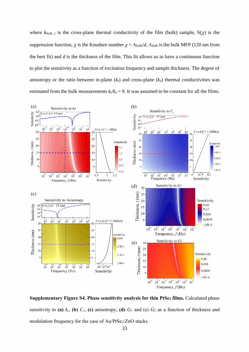
33
where kbulk, z is the cross-plane thermal conductivity of the film (bulk) sample, S() is the
suppression function, is the Knudsen number = bulk/d, bulk is the bulk MFP (120 nm from
the best fit) and d is the thickness of the film. This fit allows us to have a continuous function
to plot the sensitivity as a function of excitation frequency and sample thickness. The degree of
anisotropy or the ratio between in-plane (kr) and cross-plane (kz) thermal conductivities was
estimated from the bulk measurements kr/kz = 9. It was assumed to be constant for all the films.
Supplementary Figure S4. Phase sensitivity analysis for thin PtSe2 films. Calculated phase
sensitivity to (a) kz, (b) Cv, (c) anisotropy, (d) G1 and (e) G2 as a function of thickness and
modulation frequency for the case of Au/PtSe2/ZnO stacks.
34
The sensitivity analysis is shown over a frequency range of 20 kHz–40 MHz, where we
observed that depending on the frequency range the phase sensitivity to a given parameter
varies. For example, the sensitivity to in-plane transport for the thin films is almost zero and it
is dominant for cross-plane transport (see Fig. S4c). Moreover, from Fig. S4d,e we observe that
the sensitivity of the recorded phase signal to G1 and G2 is relatively low.
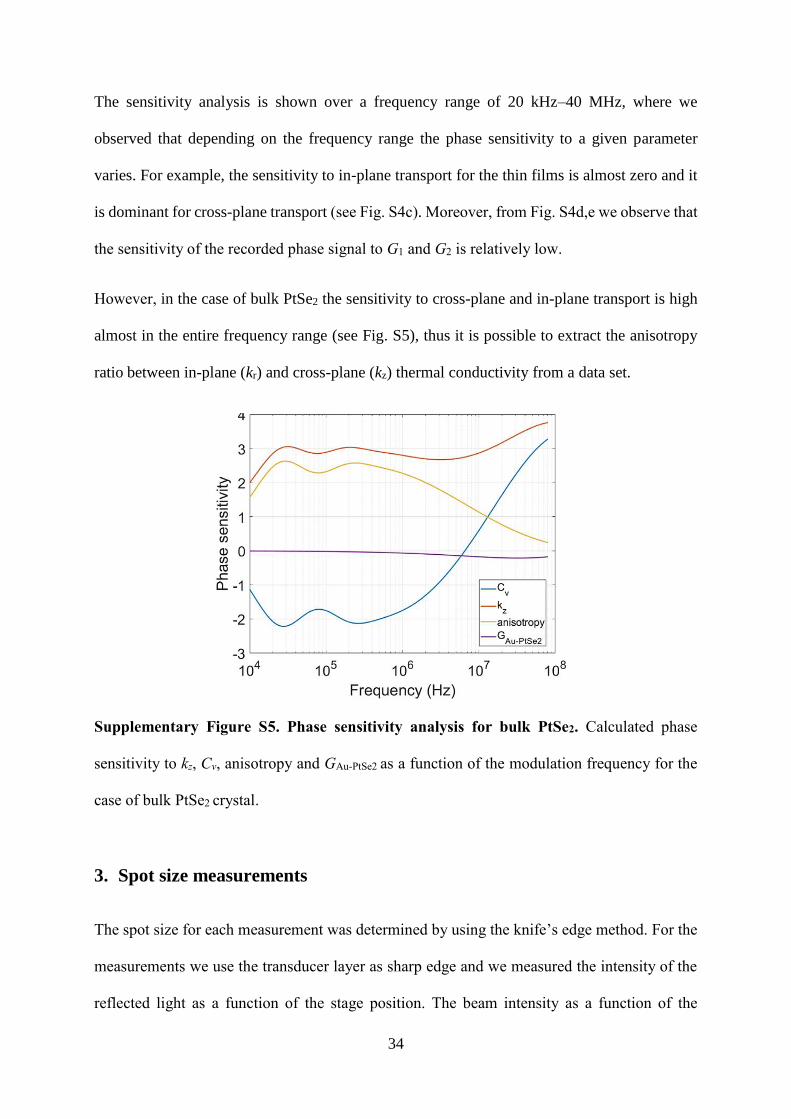
However, in the case of bulk PtSe2 the sensitivity to cross-plane and in-plane transport is high
almost in the entire frequency range (see Fig. S5), thus it is possible to extract the anisotropy
ratio between in-plane (kr) and cross-plane (kz) thermal conductivity from a data set.
Supplementary Figure S5. Phase sensitivity analysis for bulk PtSe2. Calculated phase
sensitivity to kz, Cv, anisotropy and GAu-PtSe2 as a function of the modulation frequency for the
case of bulk PtSe2 crystal.
3. Spot size measurements
The spot size for each measurement was determined by using the knife’s edge method. For the
measurements we use the transducer layer as sharp edge and we measured the intensity of the
reflected light as a function of the stage position. The beam intensity as a function of the
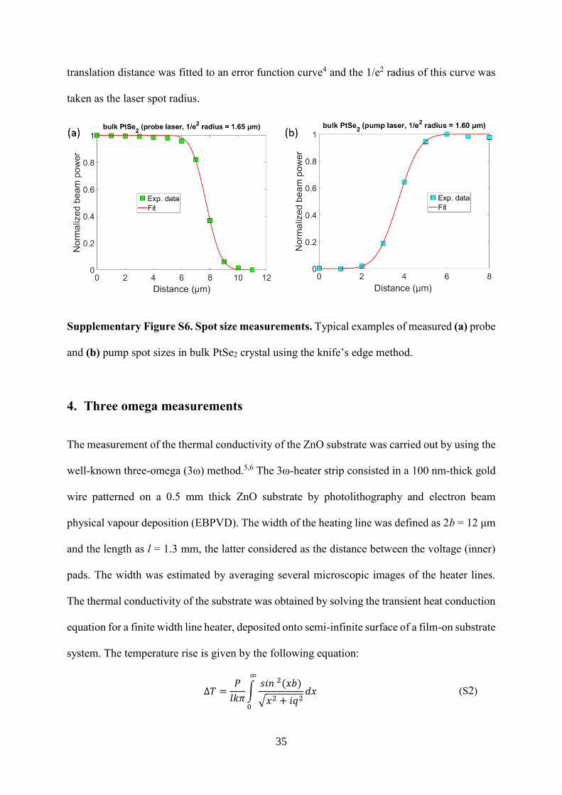
35
translation distance was fitted to an error function curve4 and the 1/e2 radius of this curve was
taken as the laser spot radius.
Supplementary Figure S6. Spot size measurements. Typical examples of measured (a) probe
and (b) pump spot sizes in bulk PtSe2 crystal using the knife’s edge method.
4. Three omega measurements
The measurement of the thermal conductivity of the ZnO substrate was carried out by using the
well-known three-omega (3ω) method.5,6 The 3ω-heater strip consisted in a 100 nm-thick gold
wire patterned on a 0.5 mm thick ZnO substrate by photolithography and electron beam
physical vapour deposition (EBPVD). The width of the heating line was defined as 2b = 12 μm
and the length as l = 1.3 mm, the latter considered as the distance between the voltage (inner)
pads. The width was estimated by averaging several microscopic images of the heater lines.
The thermal conductivity of the substrate was obtained by solving the transient heat conduction
equation for a finite width line heater, deposited onto semi-infinite surface of a film-on substrate
system. The temperature rise is given by the following equation:
Δ𝑇 =𝑃
𝑙𝑘𝜋∫
𝑠𝑖𝑛2(𝑥𝑏)
√𝑥2 + 𝑖𝑞2𝑑𝑥
∞
0
(S2)
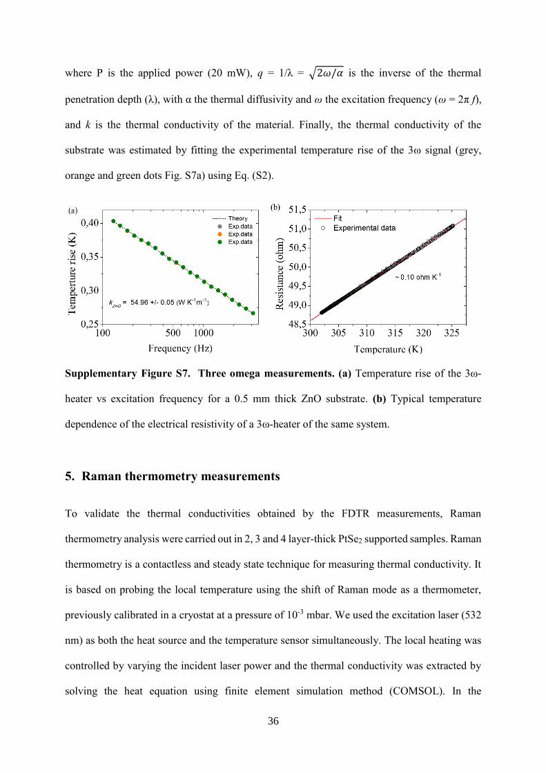
36
where P is the applied power (20 mW), q = 1/λ = √2𝜔/𝛼 is the inverse of the thermal
penetration depth (λ), with α the thermal diffusivity and ω the excitation frequency (ω = 2π f),
and k is the thermal conductivity of the material. Finally, the thermal conductivity of the
substrate was estimated by fitting the experimental temperature rise of the 3ω signal (grey,
orange and green dots Fig. S7a) using Eq. (S2).
Supplementary Figure S7. Three omega measurements. (a) Temperature rise of the 3ω-
heater vs excitation frequency for a 0.5 mm thick ZnO substrate. (b) Typical temperature
dependence of the electrical resistivity of a 3ω-heater of the same system.
5. Raman thermometry measurements
To validate the thermal conductivities obtained by the FDTR measurements, Raman
thermometry analysis were carried out in 2, 3 and 4 layer-thick PtSe2 supported samples. Raman
thermometry is a contactless and steady state technique for measuring thermal conductivity. It
is based on probing the local temperature using the shift of Raman mode as a thermometer,
previously calibrated in a cryostat at a pressure of 10-3 mbar. We used the excitation laser (532
nm) as both the heat source and the temperature sensor simultaneously. The local heating was
controlled by varying the incident laser power and the thermal conductivity was extracted by
solving the heat equation using finite element simulation method (COMSOL). In the

37
simulations, the heat power and thermal properties of the sample were given as inputs, and the
resulting temperature profile was calculated. Then, by adjusting the simulated temperature
profile to the measured one, the cross-plane thermal conductivity was obtained.
Supplementary Figure S8. Raman thermometry measurements. (a) Temperature
dependence of the Eg Raman active mode peak position. (b)-(d) Experimental temperature
rise as a function of the absorbed power.
The absorbed power was estimated by using the experimental absorption reported by Chen et
al.7 and extrapolated to our experimental data considering a 10% deviation (x-axis error bar).
For the FEM simulations, we used a Gaussian heat source given by:
Q =2AP𝐼𝜋𝑑𝜎2
exp [−2𝑟2
𝜎2] (S3)
0.0 0.5 1.0 1.5 2.00
2
4
6
8
10
12
Absorbed power [mW]
kz 0.010 [W K
-1m
-1]
kz 0.015 [W K
-1m
-1]
kz 0.030 [W K
-1m
-1]
2L Exp data
Tem
per
atu
re r
ise
[K]
(a) (b)
Fit
Exp Data
174.4
175.2
176.0
Fit
Exp Data
173.6
174.4
175.2
Fit
Exp Data
300 320 340 360 380172.8
173.6
174.4
2 layers
~ 0.020 cm-1/K
Pea
k p
osi
tio
n [
cm-1]
3 layers
~ 0.016 cm-1/K
Temperature [K]
4 layers
~ 0.018 cm-1/K
0 1 2 3 40
3
6
9
12
15
18 kz 0.025 [W K
-1m
-1]
kz 0.040 [W K
-1m
-1]
kz 0.090 [W K
-1m
-1]
4L Exp data
Tem
per
atu
re r
ise
[K]
Absorbed power [mW]
0 1 2 30
4
8
12
16
20
Absorbed power [mW]
kz 0.013 [W K
-1m
-1]
kz 0.022 [W K
-1m
-1]
kz 0.045 [W K
-1m
-1]
3L Exp data
Tem
per
atu
re r
ise
[K]
(c) (d)
38
where A is the absorption coefficient, PI is the incident power, d is the sample thickness and
is the 1/e2 radius measured in-situ using the knife’s edge method. The temperature rise in the
film (Tm) is averaged considering the real spatial temperature distribution given by:
T𝑚 =∫ 𝑟𝑇(𝑟) exp [
−2𝑟2
𝜎2]𝑑𝑟
∞
0
∫ 𝑟 exp [−2𝑟2
𝜎2]𝑑𝑟
∞
0
(S4)
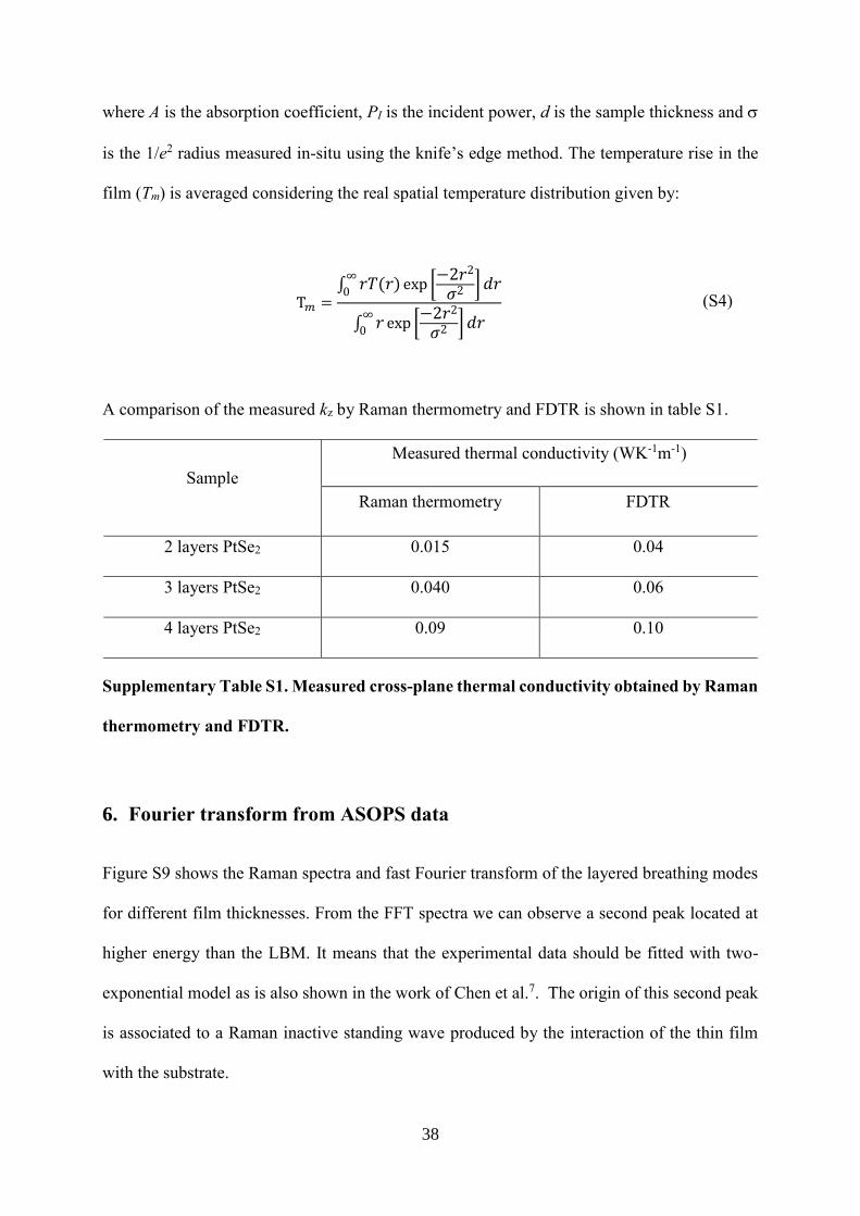
A comparison of the measured kz by Raman thermometry and FDTR is shown in table S1.
Sample
Measured thermal conductivity (WK-1m-1)
Raman thermometry FDTR
2 layers PtSe2 0.015 0.04
3 layers PtSe2 0.040 0.06
4 layers PtSe2 0.09 0.10
Supplementary Table S1. Measured cross-plane thermal conductivity obtained by Raman
thermometry and FDTR.
6. Fourier transform from ASOPS data
Figure S9 shows the Raman spectra and fast Fourier transform of the layered breathing modes
for different film thicknesses. From the FFT spectra we can observe a second peak located at
higher energy than the LBM. It means that the experimental data should be fitted with two-
exponential model as is also shown in the work of Chen et al.7. The origin of this second peak
is associated to a Raman inactive standing wave produced by the interaction of the thin film
with the substrate.
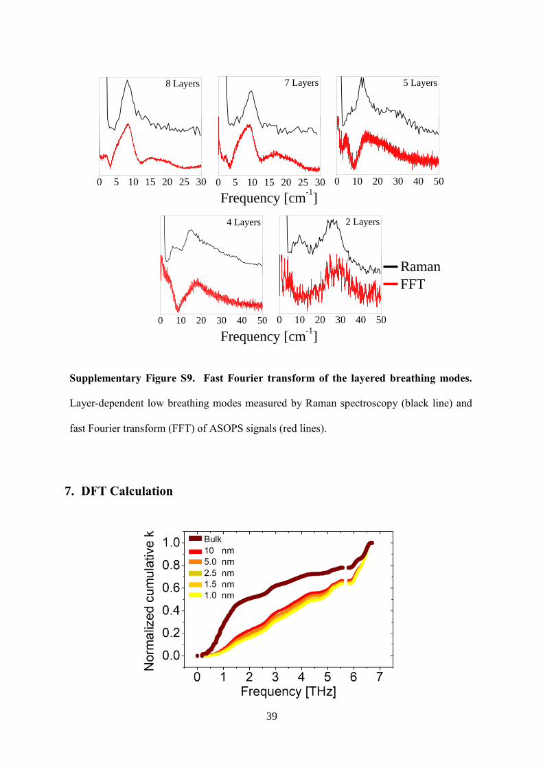
39
Supplementary Figure S9. Fast Fourier transform of the layered breathing modes.
Layer-dependent low breathing modes measured by Raman spectroscopy (black line) and
fast Fourier transform (FFT) of ASOPS signals (red lines).
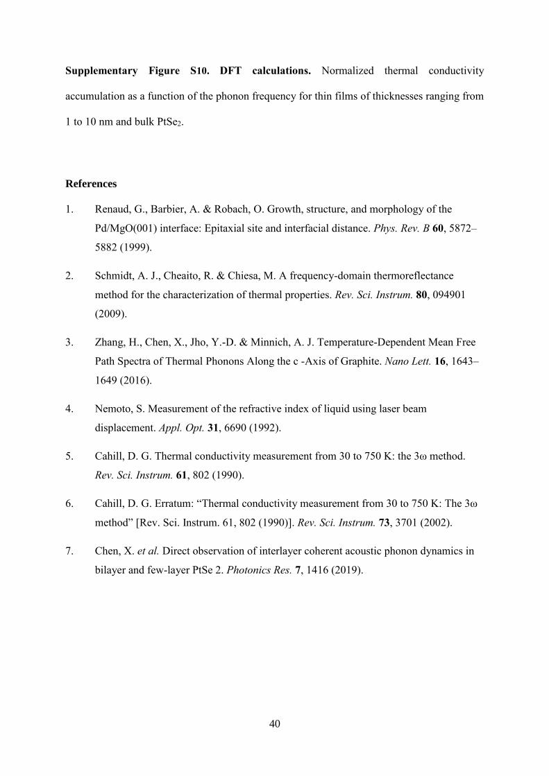
7. DFT Calculation
0 10 20 30 40 50
2 Layers
0 10 20 30 40 50
4 Layers
Frequency [cm-1]
0 10 20 30 40 50
5 Layers
0 5 10 15 20 25 30
7 Layers
0 5 10 15 20 25 30
8 Layers
Frequency [cm-1]
Raman
FFT
40
Supplementary Figure S10. DFT calculations. Normalized thermal conductivity
accumulation as a function of the phonon frequency for thin films of thicknesses ranging from
1 to 10 nm and bulk PtSe2.
References
1. Renaud, G., Barbier, A. & Robach, O. Growth, structure, and morphology of the
Pd/MgO(001) interface: Epitaxial site and interfacial distance. Phys. Rev. B 60, 5872–
5882 (1999).
2. Schmidt, A. J., Cheaito, R. & Chiesa, M. A frequency-domain thermoreflectance
method for the characterization of thermal properties. Rev. Sci. Instrum. 80, 094901
(2009).
3. Zhang, H., Chen, X., Jho, Y.-D. & Minnich, A. J. Temperature-Dependent Mean Free
Path Spectra of Thermal Phonons Along the c -Axis of Graphite. Nano Lett. 16, 1643–
1649 (2016).
4. Nemoto, S. Measurement of the refractive index of liquid using laser beam
displacement. Appl. Opt. 31, 6690 (1992).
5. Cahill, D. G. Thermal conductivity measurement from 30 to 750 K: the 3ω method.
Rev. Sci. Instrum. 61, 802 (1990).
6. Cahill, D. G. Erratum: “Thermal conductivity measurement from 30 to 750 K: The 3ω
method” [Rev. Sci. Instrum. 61, 802 (1990)]. Rev. Sci. Instrum. 73, 3701 (2002).
7. Chen, X. et al. Direct observation of interlayer coherent acoustic phonon dynamics in
bilayer and few-layer PtSe 2. Photonics Res. 7, 1416 (2019).