
Philips Bdp-7500b2 Sm (1)
55
Published by KC-LQ 1027 AVM Printed in the Netherlands BDP7500B2 Subject to modification EN Blue-Ray Disc Player Contents Page Contents Page © Copyright 2010 Philips Consumer Electronics B.V. Eindhoven, The Netherlands. All rights reserved. No part of this publication may be reproduced, stored in a retrieval system or transmitted, in any form or by any means, electronic, mechanical, photocopying, or otherwise without the prior permission of Philips. Version 1.1 1 Technical Specification and Connection Facilities and Version variation 2 Laser Beam Safety Precautions..................................2-1 3 Important Safety Precautions ......................... 3-1 to 3-2 4 Safety Check After Servicing .................................... 4-1 6 Standard Notes For Servicing .................................. .6-1 7 Special Information BGA IC & Flat Pack-IC 5 Safety Information General Notes & Lead Free 8 Direction of Use ...............................................8-1 to 8-5 9 Cabinet Disassembly Instructions ................... 9-1 to 9-2 15 Main Unit--MCD Board 10 Troubleshooting ......................................... 10-1 to 10-2 11 Software Upgrading Procedure ............................. 11-1 12 Software Version Check ........................................ 12-1 13 Block Diagram ........................................................13-1 14 Wiring Diagram ...................................................... 14-1 16 Main Unit--VFD Display Board 17 Main Unit-- Touch Board Layout Diagram ................................ 17-1 18 Main Unit--Decoder Board 19 Main Unit--Power Board 21 Main Unit Exploded View .......................................21-1 22 Packing Exploded View ..........................................22-1 23 OPU setting alignment procedure .........................23-1 20 Main Unit--Output Board ................................................... 7-1 to 7-3 Circuit Diagram ..................18-1 to 18-12 Circuit Diagram ...............................19-1 Circuit Diagram ...............................20-1 Layout Diagram .............................18-13 Layout Diagram ..............................19-2 Layout Diagram ..............................20-2 ..............................................1-1 to 1-3 Circuit Diagram ................................. 15-1 Layout Diagram ................................ 15-2 Circuit Diagram ................................. 16-1 Circuit Diagram ................................. 17-1 Layout Diagram ................................ 16-2 Requirement ............................ 5-1 to 5-2 24 Revision List ...........................................................24-1 314178534981
-
Upload
jose-koc-gongora -
Category
Documents
-
view
27 -
download
0
description
Manual de Servicio BDP 7500B2 Philips
Transcript of Philips Bdp-7500b2 Sm (1)

Published by KC-LQ 1027 AVM Printed in the Netherlands
BDP7500B2
Subject to modification EN
Blue-Ray Disc Player
Contents Page Contents Page
©Copyright 2010 Philips Consumer Electronics B.V. Eindhoven, The Netherlands.All rights reserved. No part of this publication may be reproduced, stored in a retrieval system or transmitted, in any form or by any means, electronic, mechanical, photocopying, or otherwise without the prior permission of Philips.
Version 1.1
1 Technical Specification and Connection Facilities andVersion variation
2 Laser Beam Safety Precautions..................................2-13 Important Safety Precautions ......................... 3-1 to 3-24 Safety Check After Servicing .................................... 4-1
6 Standard Notes For Servicing .................................. .6-17 Special Information BGA IC & Flat Pack-IC
5 Safety Information General Notes & Lead Free
8 Direction of Use ...............................................8-1 to 8-59 Cabinet Disassembly Instructions ................... 9-1 to 9-2
15 Main Unit--MCD Board
10 Troubleshooting ......................................... 10-1 to 10-211 Software Upgrading Procedure ............................. 11-112 Software Version Check ........................................ 12-113 Block Diagram ........................................................13-114 Wiring Diagram ...................................................... 14-1
16 Main Unit--VFD Display Board
17 Main Unit-- Touch Board
Layout Diagram ................................ 17-118 Main Unit--Decoder Board
19 Main Unit--Power Board
21 Main Unit Exploded View .......................................21-1
22 Packing Exploded View ..........................................22-1
23 OPU setting alignment procedure .........................23-1
20 Main Unit--Output Board
................................................... 7-1 to 7-3
Circuit Diagram ..................18-1 to 18-12
Circuit Diagram ...............................19-1
Circuit Diagram ...............................20-1
Layout Diagram .............................18-13
Layout Diagram ..............................19-2
Layout Diagram ..............................20-2
..............................................1-1 to 1-3
Circuit Diagram ................................. 15-1Layout Diagram ................................ 15-2
Circuit Diagram ................................. 16-1
Circuit Diagram ................................. 17-1
Layout Diagram ................................ 16-2
Requirement ............................ 5-1 to 5-2
24 Revision List ...........................................................24-1
314178534981

1.1 PCB Locations
1.2 General:
Power supply : 100-240V, 50Hz~60HzPower consumption : 35W
AmpliferStandby power consumption : < 1 W
1.3
est equipment: Fluke 54200est streams: Philips Standard test pattern
1.5 AUDIO Performance:
1-1
VFD Display Board
Decoder Board
MCU BoardTouch Board
Led Board
Digital Signals Board
Power Board

Technical Speci cations and Connection Facilities
1.6 Analog Video Preformance
1.6.1 CVBS Output Component
Amplitude Output : 1000mVpp ± 10%White Bar : 714mVpp ± 10%Sync. Amplitude : 286mVpp ± 10%
Chroma / Luminunce Delay(2T pulse)
Amplitude Output : 1000mVpp ± 10%White Bar : 714mVpp ± 10%Sync. Amplitude : 286mVpp ± 10%
Chroma / Luminunce Delay(2T pulse)
1.6.2 Video Output Component
COMPONENT VIDEO OUT – Cinch (Y/Pb/Pr):According to EIA-770-1-A, EIA-770-2-A
1.7 Digital Inputs
1.7.1 (AUDIO OUT) COAXIAL DIGITAL OUT – Cinch
LPCM : according IEC 60958-3MPEG 1, MPEG 2, AC3 : according IEC 61937DTS : according IEC 61937 +
addendum
1.7.2 USB
Compatibility : USB 2.0 Type of connector : Series A Connector
1.7.3 HDMI Output
Compatibility : HDMI version 1.3 Type of connector : Type A connector
(19 pins)
1.8 Video Performance
1.8.1 SNR
PAL
RGB CVBS Y/C
Y
NTSC
Y Pb Pr CVBS Y/C
Y
1.8.2 Bandwidth
PAL
RGB CVBS Y/C
0.5 to 4 MHz:+1dB/ -2dB
0.5 to 4 MHz:+1dB/ -2dB
Y:4.8MHz-3dB
4.8 MHz:-3dB 4.8 MHz:-3dB C:700 kHz
5.8 MHz:-6dB 5.8 MHz:-6dB
NTSC
YPbPr CVBS Y/C
4.2 MHz:-3dB 4.2 MHz:-3dB Y:4.2MHz-3dB
5.8 MHz:-6dB 5.8 MHz:-6dB
With Pscan: 8.4MHz -3dB
1-2

Technical Specifications and Connection Facilities
1.9 Dimension and WeightSet Dimension W x H x D : 790.6 x 145 x 57.4 mmNet Weight : 2.23 kgSubwoofer Dimension W x H x D : 182 x 365 x 306 mmNet Weight : 6 kg
2.0 Laser Output Power & Wavelength
2.0.1 DVD
Output power during reading : 7mWOutput power during writing : 6mWWavelength : 80nm (at 25 °C)
2.0.2 CD
Output power : 6mWWavelength : 60nm (at 25 °C)
2.1 Playability
Video Playback1. Playback Media:
CD-R/CD-RW, DVD+R/+RW, DVD-R/-RW, DVD-Video, Video CD/SVCD, DVD+R DL, DVD-R DL, USB flash drive
x
2. Compression Formats:MPEG2, MPEG1, DivX 3.11, DivX 4.x, DivX 5.x, DivX 6.0, MPEG4
x
Audio Playback1. Playback Media:
Audio CD, CD-R/RW, DVD+R DL, DVD+R/+RW, DVD-R/-RW, MP3-CD, MP3-DVD, USB flash drive, WMA-CD
x
2. Compression Format:Dolby Digital, MP3, MPEG2 Multichannel, PCM, WMA
x
3. MPEG1 bit rates: 64-384 kbps and VBR
x
Still Picture Playback1. Playback Media: CD-R/RW,
DVD+R DL, DVD+R/+RW, DVD-R/-RW, Picture CD, USB Digital Camera (PTP), USB flash drive
x
2. Picture Compression Format:JPEG, JPEG digital camera photos
x
3. Picture enhancement: Slideshow with MP3 playback, Create albums, Rotate, Slideshow with music playback, Zoom
x
1-3
Type /Versions:
Features
Board in used:
BDP7500B2
Service policy
VFD DISPLAY BOARD
* TIPS : C -- Component Lever Repair.M -- Module Lever Repair√ -- Used
Feature diffrenceRDS VOLTAGE SELECTORECO STANDBY
Type /Versions:
12/
VERSION VARIATION
C
√
DECODER BOARD
BDP7500B2
CC
DIGITAL SIGNALS BOARD
C
/98
DTS √
POWER BOARD
MCU BOARD
MM
/05 /51 /55
√√
√√
√√
√√
12/ /98/05 /51 /55
TOUCH BOARDLED BOARD
M
CCMMM
C/MC/MC
MC
MM
C/MC/M

Laser Beam Safety Precautions
This Blu-Ray player uses a pickup that emits a laser beam.
The laser beam is emitted from the location shown in the figure. When checking the laser diode, be sure to keepyour eyes at least 30 cm away from the pickup lens when the diode is turned on. Do not look directly at the laserbeam.
CAUTION: Use of controls and adjustments, or doing procedures other than those specified herein, may result inhazardous radiation exposure.
Location: Inside Top of Blu-Ray mechanism.
Do not look directly at the laser beam comingfrom the pickup or allow it to strike against yourskin.
Drive Mechanism Assembly
Laser Beam Radiation
Laser Pickup
Turntable
2-1

Electronics N.V. bears no responsibilityfor improper wall mounting that results inaccident, injury or damage.
For speakers with stands, use only thesupplied stands. Secure the stands tothe speakers tightly. Place the assembledstands on t, level surfaces that cansupport the combined weight of thespeaker and stand.Never place the product or any objectson power cords or on other electricalequipment.If the product is transported intemperatures below 5°C, unpack theproduct and wait until its temperaturematches room temperature beforeconnecting it to the power outlet.Visible and invisible laser radiation whenopen. Avoid exposure to beam.Do not touch the disc optical lens insidethe disc compartment.
Risk of overheating!Never install this product in a con nedspace. Always leave a space of at leastfour inches around the product forventilation. Ensure curtains or otherobjects never cover the ventilation slotson the product.
Risk of contamination!Do not mix batteries (old and new orcarbon and alkaline, etc.).Remove batteries if they are exhaustedor if the remote control is not to be usedfor a long time.Batteries contain chemical substances,they should be disposed of properly.
Product careDo not insert any objects other than discsinto the disc compartment.Do not insert warped or cracked discsinto the disc compartment.Remove discs from the disc compartmentif you are not using the product for anextended period of time.
•
•
•
•
•
•
•
•
•
•
•
•
Only use microfiber cloth to clean theproduct.
•
Important
Important Safety Precautions
Read and understand all instructions before you useyour home theater. If damage is caused by failure to follow instructions, the warranty does not apply.
SafetyRiskof electricshockor re!
Never expose the product andaccessories to rain or water. Never placeliquid containers, such as vases, near theproduct. If liquids are spilt on or into theproduct, disconnect it from the poweroutlet immediately. Contact PhilipsConsumer Care to have the productchecked before use.Never place the product and accessoriesnear naked ames or other heat sources,including direct sunlight.Never insert objects into the ventilationslots or other openings on the product.Where the mains plug or an appliancecoupler is used as the disconnect device,the disconnect device shall remain readilyoperable.Disconnect the product from the poweroutlet before lightning storms.When you disconnect the power cord,always pull the plug, never the cable.
Riskof short circuit or re!Before you connect the product to thepower outlet, ensure that the powervoltage matches the value printed on theback or bottom of the product. Neverconnect the product to the power outletif the voltage is different.
Risk of injury or damage to the home theater!For wall-mountable products, use onlythe supplied wall mount bracket. Securethe wall mount to a wall that can supportthe combined weight of the productand the wall mount. Koninklijke Philips
•
•
•
•
•
•
•
•
3-1

User manual CDTo read the complete user manual, which includes information on advanced features, use the CD supplied with your home theater. For a printed copy of the complete user manual,contact Philips Consumer Care in your country.
To access the user manual
Caution
The user manual CD is for PC or Mac only. Donot insert the user manual CD into the disccompartment of the home theater.
•
Requirements:A PC (Microsoft Windowscompatible) or Mac (OS X) withCD-ROMAdobe Reader
1 Insert the user manual CD into the CD-ROM tray of the PC or Mac.
2 Close the CD-ROM tray.The user manual screen appears. If the user manual screen does not appear,skip Step 3 and navigate to the ‘pdf ’folder in the CD-ROM, double-clickingthe PDF of your choice.
3 Click a user manual language.Acrobat Reader launches, displayingthe complete user manual in the language of your choice.
•
•
»
»
Disposal of your old product and batteries
Your product is designed and manufacturedwith high quality materials and components,which can be recycled and reused.
When this crossed-out wheeled bin symbolis attached to a product it means that theproduct is covered by the European Directive2002/96/EC. Please inform yourself about thelocal separate collection system for electricaland electronic products.Please act according to your local rules anddo not dispose of your old products with yournormal household waste.Correct disposal of your old product helps toprevent potential negative consequences forthe environment and human health.
Your product contains batteries covered by the European Directive 2006/66/EC, whichcannot be disposed with normal householdwaste.Please inform yourself about the local ruleson separate collection of batteries becausecorrect disposal helps to prevent negativeconsequences for the environmental andhuman health.
Important Safety Precautions
3-2

4-1
Safety Check after Servicing
Examine the area surrounding the repaired location for damage or deterioration. Observe that screws, parts, andwires have been returned to their original positions. Afterwards, do the following tests and confirm the specifiedvalues to verify compliance with safety standards.
1. Clearance DistanceWhen replacing primary circuit components, confirmspecified clearance distance (d) and (d’) betweensoldered terminals, and between terminals andsurrounding metallic parts. (See Fig. 1)
Table 1: Ratings for selected area
Note: This table is unofficial and for reference only. Besure to confirm the precise values.
2. Leakage Current TestConfirm the specified (or lower) leakage currentbetween B (earth ground, power cord plug prongs) andexternally exposed accessible parts (RF terminals,antenna terminals, video and audio input and outputterminals, microphone jacks, earphone jacks, etc.) islower than or equal to the specified value in the tablebelow.
Measuring Method (Power ON):
Insert load Z between B (earth ground, power cord plugprongs) and exposed accessible parts. Use an ACvoltmeter to measure across the terminals of load Z.See Fig. 2 and the following table.
Table 2: Leakage current ratings for selected areas
Note: This table is unofficial and for reference only. Be sure to confirm the precise values.
AC Line Voltage Clearance Distance (d), (d’)
110V~220V 3.2 mm (0.126 inches)
AC Line Voltage Load Z Leakage Current (i) Earth Ground (B) to:
110V~220V 0.15 µF CAP. & 1.5 k RES.Connected in parallel i 0.5 mA Peak Exposed accessible parts
Chassis or Secondary Conductor
Primary Circuit
Fig. 1
d' d
AC Voltmeter(High Impedance)
Exposed Accessible Part
B Earth Ground Power Cord Plug Prongs
Z
Fig. 2

1 Safety Instructions
1.1 General Safety
Safety regulations require that during a repair:• Connect the unit to the mains via an isolation transformer.• Replace safety components, indicated by the symbol ,
only by components identical to the original ones. Anyother component substitution (other than original type)
Safety regulations require that after a repair, you must returnthe unit in its original condition. Pay, in particular, attention tothe following points:• Route the wires/cables correctly
mounted cable clamps.•
damage.• Check the electrical DC resistance between the mains
plug and the secondary side:1. Unplug the mains cord, and connect a wire between
the two pins of the mains plug.2. Set the mains switch to the ‘on’ position (keep the
mains cord unplugged!).3. Measure the resistance value between the mains
plug and the front panel, controls, and chassisbottom.
4. Repair or correct unit when the resistance
5. Verify this, before you return the unit to the customer/user (ref. UL-standard no. 1492).
6. Switch the unit ‘off’, and remove the wire between the two pins of the mains plug.
1.2 Laser Safety
This unit employs a lasermay remove the cover, or attempt to service this device (dueto possible eye injury).
Laser Device UnitresalrotcudnocimeS:epyT
sAlAaGWavelength : 650 nm (DVD)
)DC/DCV(mn087:Output Power : 20 mW
)gnitirwWR+DVD(Wm8.0:
)gnidaerDVD(Wm3.0:
)gnidaerDC/DCV(Beam divergence : 60 degree
CLASS 1LASER PRODUCT
1-2erugiF
Note: Use of controls or adjustments or performance ofprocedure other than those speci ed herein, may result in
A
2 Warnings
2.1 General
• All ICs and many other semiconductors are susceptible to electrostatic discharges (ESD, ). Careless handlingduring repair can reduce life drastically. Make sure that, during repair, you are at the same potential as the massof the set by a wristband with resistance. Keep components and tools at this same potential.Available ESD protection equipment:– Complete kit ESD3 (small tablemat, wristband,
4822 310 10671.– Wristband tester 4822 344 13999.
• Be careful during measurements in the live voltagesection. The primary side of the power supply, includingthe heatsink, carries live mains voltage when youconnect the player to the mains (even when the player is ‘off’!). It is possible to touch copper tracks and/ or components in this unshielded primary area, whenyou service the player. Service personnel must takeprecautions to prevent touching this area or componentsin this area. A ‘lightning stroke’ and a stripe-markedprinting on the printed wiring board, indicate the primaryside of the power supply.
• Never replace modules, or components, while the unit is‘on’.
2.2 Laser
• The use of optical instruments with this product, will
• Only quali ed service personnel may remove the cover orattempt to service this device, due to possible eye injury.
• Repair handling should take place as much as possiblewith a disc loaded inside the player.
• Tshield:
Figure 2-2
Safety Information, General Notes & Lead Free Requirements
CAUTION VISIBLE AND INVISIBLE LASER RADIATION WHEN OPEN AVOID EXPOSURE TO BEAMADVARSEL SYNLIG OG USYNLIG LASERSTRÅLING VED ÅBNING UNDGÅ UDSÆTTELSE FOR STRÅLINGADVARSEL SYNLIG OG USYNLIG LASERSTRÅLING NÅR DEKSEL ÅPNES UNNGÅ EKSPONERING FOR STRÅLENVARNING SYNLIG OCH OSYNLIG LASERSTRÅLNING NÄR DENNA DEL ÄR ÖPPNAD BETRAKTA EJ STRÅLENVARO! AVATTAESSA OLET ALTTIINA NÄKYVÄLLE JA NÄKYMÄTTÖMÄLLE LASER SÄTEILYLLE. ÄLÄ KATSO SÄTEESEENVORSICHT SICHTBARE UND UNSICHTBARE LASERSTRAHLUNG WENN ABDECKUNG GEÖFFNET NICHT DEM STRAHL AUSSETSENDANGER VISIBLE AND INVISIBLE LASER RADIATION WHEN OPEN AVOID DIRECT EXPOSURE TO BEAMATTENTION RAYONNEMENT LASER VISIBLE ET INVISIBLE EN CAS D’OUVERTURE EXPOSITION DANGEREUSE AU FAISCEAU
5-1

Safety Information, General Notes & Lead Free Requirements
3 Lead Free Requirement
Information about Lead-free produced sets
Philips CE is starting production of lead-free sets from1.1.2005 onwards.
INDENTIFICATION:
Regardless of special logo (not always indicated)
One must treat all sets from 1 Jan 2005 onwards, accordingnext rules.
Example S/N:
Bottom line of typeplate gives a 14-digit S/N. Digit 5&6 is the year, digit 7&8 is the week number, so in this case 1991 wk 18
So from 0501 onwards = from 1 Jan 2005 onwards
Important note: In fact also products of year 2004 must be treated in this way as long as you avoid mixing solder-alloys (leaded/ lead-free). So best to always use SAC305 and the highertemperatures belong to this.
Due to lead-free technology some rules have to be respected by the workshop during a repair:
Use only lead-free solder alloy Philips SAC305 with order code 0622 149 00106. If lead-free solder-pate is required, please contact the manufacturer of your solder-equipment. In general use of solder-paste within workshops should be avoided because paste is not easy to store and to handle.
Use only adequate solder tools applicable for lead-free solder alloy. The solder tool must be able
o To reach at least a solder-temperature of 400°C, o To stabilize the adjusted temperature at the solder-
tip o To exchange solder-tips for different applications.Adjust your solder tool so that a temperature around
360°C – 380°C is reached and stabilized at the solder joint. Heating-time of the solder-joint should not exceed ~ 4 sec. Avoid temperatures above 400°C otherwise wear-out of tips will rise drastically and destroyed. To avoid wear-out of tips switch off un-used equipment, or reduce heat.
Mix of lead-free solder alloy / parts with leaded solder alloy / parts is possible but PHILIPS recommends stronglyto avoid mixed solder alloy types (leaded and lead-free). If one cannot avoid or does not know whether product is lead-free, clean carefully the solder-joint from old solder alloy and re-solder with new solder alloy (SAC305).
Use only original spare-parts listed in the Service-Manuals. Not listed standard-material (commodities) has
to be purchased at external companies.Special information for BGA-ICs:
- always use the 12nc-recognizable soldering temperature A (for de-soldering always use
the lead-free temperature pro le, in case of doubt) - lead free BGA-ICs will be delivered in so-called ‘dry-packaging’ (sealed pack including a silica gel pack) to protect the IC against moisture. After opening, dependent of MSL-level seen on indicator-label in the bag, the BGA-IC possibly still has to be baked dry. (MSL=Moisture Sensitivity Level). This will be communicated via AYS-website.
Do not re-use BGAs at all.
For sets produced before 1.1.2005 (except products of 2004), containing leaded solder-alloy and components, all needed spare-parts will be available till the end of the service-period. For repair of such sets nothing changes.
On our website www.atyourservice.ce.Philips. com
BGA-de-/soldering (+ baking instructions)Heating-pro les of BGAs and other ICs used in Philips-
sets
You will nd this and more technical information within the “magazine”, chapter “workshop news”.
For additional questions please contact your local repair-helpdesk.
5-2

6-1
Standard Notes for Servicing
Circuit Board Indications1. The output pin of the 3 pin Regulator ICs is
indicated as shown.
2. For other ICs, pin 1 and every fifth pin areindicated as shown.
3. The 1st pin of every male connector is indicated asshown.
Instructions for Connectors1. When you connect or disconnect the FFC (Flexible
Foil Connector) cable, be sure to first disconnectthe AC cord.
2. FFC (Flexible Foil Connector) cable should beinserted parallel into the connector, not at anangle.
Pb (Lead) Free SolderWhen soldering, be sure to use the Pb free solder.
Information about lead-free soldering
Philips CE is producing lead-free sets from 1.1.2005onwards.
IDENTIFICATIONRegardless of special logo (not alwaysindicated)
One must treat all sets fromonwards, according to the next rule:Serial Number gives a 14-digit. Digit 5&6 shows theYEAR, and digit 7&8 shows the WEEK.
So from onwards=from 1 Jan 2005 onwards
Important note : In fact also products of year 2004must be treated in this way as long as you avoidmixing solder-alloys (leaded/ lead-free). So best toalways use SAC305 and the higher temperaturesbelong to this.
Due to lead-free technology some rules have to berespected by the workshop during a repair:• Use only lead-free solder alloy Philips SAC305 with
order code 0622 149 00106. If lead-free solder-paste is required, please contact the manufacturerof your solder-equipment. In general use of solder-paste within workshops should be avoided becausepaste is not easy to store and to handle.
• Use only adequate solder tools applicable for lead-free solder alloy. The solder tool must be able• To reach at least a solder-temperature of 400°C,• To stabilize the adjusted temperature at the solder-
tip• To exchange solder-tips for different applications.
• Adjust your solder tool so that a temperature around360°C - 380°C is reached and stabilized at thesolder joint. Heating-time of the solder-joint shouldnot exceed ~ 4 sec. Avoid temperatures above400°C otherwise wear-out of tips will rise drasticallyand flux-fluid will be destroyed. To avoid wear-out oftips switch off un-used equipment, or reduce heat.
• Mix of lead-free solder alloy / parts with leadedsolder alloy / parts is possible but PHILIPSrecommends strongly to avoid mixed solder alloytypes (leaded and lead-free).If one cannot avoid or does not know whetherproduct is lead-free, clean carefully the solder-jointfrom old solder alloy and re-solder with new solderalloy (SAC305).
• Use only original spare-parts listed in the Service-Manuals. Not listed standard-material (commodities)has to be purchased at external companies.
Top View
Out In
Bottom ViewInput
5
10
Pin 1
Pin 1
FFC Cable
Connector
CBA
* Be careful to avoid a short circuit.
1 Jan 2005
0501

7-1
• Special information for BGA-ICs:- always use the 12nc-recognizable solderingtemperature profile of the specific BGA (for de-soldering always use the lead-free temperatureprofile, in case of doubt)- lead free BGA-ICs will be delivered in so-called'dry-packaging' (sealed pack including a silica gelpack) to protect the IC against moisture. Afteropening, dependent of MSL-level seen on indicator-label in the bag, the BGA-IC possibly still has to bebaked dry. (MSL=Moisture Sensitivity Level). Thiswill be communicated via AYS-website.Do not re-use BGAs at all.
• For sets produced before 1.1.2005 (except productsof 2004), containing leaded solder-alloy andcomponents, all needed spare-parts will be availabletill the end of the service-period. For repair of suchsets nothing changes.
• On our websitewww.atyourservice.ce.Philips.com you find moreinformation to:• BGA-de-/soldering (+ baking instructions)• Heating-profiles of BGAs and other ICs used in
Philips-sets
You will find this and more technical information withinthe “magazine”, chapter “workshop news”.
For additional questions please contact your localrepair-helpdesk.
How to Remove / Install Flat Pack-IC
Special Information of BGA IC & Flat Pack-IC
1. RemovalWith Hot-Air Flat Pack-IC Desoldering Machine:1. Prepare the hot-air flat pack-IC desoldering
machine, then apply hot air to the Flat Pack-IC(about 5 to 6 seconds). (Fig. S-1-1)
2. Remove the flat pack-IC with tweezers whileapplying the hot air.
3. Bottom of the flat pack-IC is fixed with glue to theCBA; when removing entire flat pack-IC, first applysoldering iron to center of the flat pack-IC and heatup. Then remove (glue will be melted). (Fig. S-1-6)
4. Release the flat pack-IC from the CBA usingtweezers. (Fig. S-1-6)
CAUTION:1. The Flat Pack-IC shape may differ by models. Use
an appropriate hot-air flat pack-IC desolderingmachine, whose shape matches that of the FlatPack-IC.
2. Do not supply hot air to the chip parts around theflat pack-IC for over 6 seconds because damageto the chip parts may occur. Put masking tapearound the flat pack-IC to protect other parts fromdamage. (Fig. S-1-2)
Fig. S-1-1

3. The flat pack-IC on the CBA is affixed with glue, sobe careful not to break or damage the foil of eachpin or the solder lands under the IC whenremoving it.
With Soldering Iron:1. Using desoldering braid, remove the solder from
all pins of the flat pack-IC. When you use solderflux which is applied to all pins of the flat pack-IC,you can remove it easily. (Fig. S-1-3)
2. Lift each lead of the flat pack-IC upward one byone, using a sharp pin or wire to which solder willnot adhere (iron wire). When heating the pins, usea fine tip soldering iron or a hot air desolderingmachine. (Fig. S-1-4)
3. Bottom of the flat pack-IC is fixed with glue to theCBA; when removing entire flat pack-IC, first applysoldering iron to center of the flat pack-IC and heatup. Then remove (glue will be melted). (Fig. S-1-6)
4. Release the flat pack-IC from the CBA usingtweezers. (Fig. S-1-6)
With Iron Wire:1. Using desoldering braid, remove the solder from
all pins of the flat pack-IC. When you use solderflux which is applied to all pins of the flat pack-IC,you can remove it easily. (Fig. S-1-3)
2. Affix the wire to a workbench or solid mountingpoint, as shown in Fig. S-1-5.
3. While heating the pins using a fine tip solderingiron or hot air blower, pull up the wire as the soldermelts so as to lift the IC leads from the CBAcontact pads as shown in Fig. S-1-5.
4. Bottom of the flat pack-IC is fixed with glue to theCBA; when removing entire flat pack-IC, first applysoldering iron to center of the flat pack-IC and heatup. Then remove (glue will be melted). (Fig. S-1-6)
5. Release the flat pack-IC from the CBA usingtweezers. (Fig. S-1-6)
Note: When using a soldering iron, care must betaken to ensure that the flat pack-IC is notbeing held by glue. When the flat pack-IC isremoved from the CBA, handle it gentlybecause it may be damaged if force is applied.
Hot-airFlat Pack-ICDesolderingMachineCBA
Flat Pack-IC
Tweezers
MaskingTape
Fig. S-1-2
Flat Pack-IC Desoldering Braid
Soldering Iron
Fig. S-1-3
Fine TipSoldering Iron
SharpPin
Fig. S-1-4
To Solid Mounting Point
Soldering Iron
Iron Wire
or
Hot Air Blower
Fig. S-1-5
Fine TipSoldering IronCBA
Flat Pack-ICTweezers
Fig. S-1-6
7-2

7-3
2. Installation1. Using desoldering braid, remove the solder from
the foil of each pin of the flat pack-IC on the CBAso you can install a replacement flat pack-IC moreeasily.
2. The “ ” mark on the flat pack-IC indicates pin 1.(See Fig. S-1-7.) Be sure this mark matches the 1on the PCB when positioning for installation. Thenpresolder the four corners of the flat pack-IC. (SeeFig. S-1-8.)
3. Solder all pins of the flat pack-IC. Be sure thatnone of the pins have solder bridges.
Instructions for Handling Semi-
Special Information BGA IC & Flat Pack-IC
conductorsElectrostatic breakdown of the semi-conductors mayoccur due to a potential difference caused byelectrostatic charge during unpacking or repair work.
1. Ground for Human BodyBe sure to wear a grounding band (1 M ) that isproperly grounded to remove any static electricity thatmay be charged on the body.
2. Ground for WorkbenchBe sure to place a conductive sheet or copper platewith proper grounding (1 M ) on the workbench orother surface, where the semi-conductors are to beplaced. Because the static electricity charge onclothing will not escape through the body groundingband, be careful to avoid contacting semi-conductorswith your clothing.
Example :
Pin 1 of the Flat Pack-ICis indicated by a " " mark. Fig. S-1-7
Presolder
CBA
Flat Pack-IC
Fig. S-1-8
<Incorrect>
CBA
Grounding Band
Conductive Sheet orCopper Plate
1M
1M
<Correct>
CBA

Direction of Use
8-3
Option 1: Connect to the HDMI jack
1 Connect an HDMI cable (not supplied) to:the• HDMI jack on this product.the HDMI input jack on the TV.•
Tip
If the TV has a DVI connector only, connect via an HDMI/•DVI adaptor. Connect an audio cable for sound output.You can optimize the video output. Press the• HDMIbutton repeatedly to select the best resolution the TVcan support.If this product connects to a TV compatible with 1080p•or 1080p/24Hz, Philips recommends HDMI category 2 cable, also known as High Speed HDMI cable, for optimalvideo and audio output.To play the digital video images of a BD-video or DVD-•video via an HDMI connection, it is necessary that boththis product and the display device (or an AV receiver/ampl er) support a copyright protection system calledHDCP (high-bandwidth digital content protection system).This type of connection provides best picture quality.•
Option 2: Connect to the component video jack
1 Connect the component video cables(not supplied) to:
HDMI IN
PbY Pr
AUDIO IN
the• Y Pb/Cb Pr/Crjacks on this product.the COMPONENT VIDEO input jacks•on the TV.
2 Connect the audio cables to:the• LINE OUT/AUDIO -L/Rjacks onthis product.the AUDIO input jacks on the TV.•
Tip
The component video input jack on the TV might be•labeled as Y Pb Pr or YUV.
Option 3: Connect to the composite video jack
1 Connect a composite video cable to:the• VIDEOjack on this product.the VIDEO input jack on the TV.•
2 Connect the audio cables to:the• LINE OUT/AUDIO-L/Rjacks on thisproduct.the AUDIO input jacks on the TV.•
Tip
The video input jack on the TV might be labeled as A/V•IN, VIDEO IN, COMPOSITE or BASEBAND.
Route audio to other devicesYou can route the audio from this product to other devices.
AUDIO IN
VIDEO IN

Direction of Use
8-4
Connect to HDMI-compliant AV receiver/
1 Connect an HDMI cable (not supplied) to:the• HDMI jack on this product.the HDMI jack input jack on the device.•
Tip
The HDMI connection provides best audio quality.•
Connect to multi-channel AV receiver/
1 Connect the 7.1-channel audio cables (notsupplied) to:
the• 7.1 CH AUDIO OUTPUTjacks onthis product.the corresponding AUDIO input jacks•on the device.
HDMI IN
7.1 CH AU DIO IN
Tip
To connect 5.1-channel AV receiver/ampli er, connect•the 7.1-channel audio jacks except the SL/SR jacks.You can optimize the speaker output (see “Adjust•settings” > [Audio Setup] >[Speaker Setup] ).
Connect to digital A receiverConnect to coaxial jack
COAXIAL
COAXIAL
1 Connect a coaxial cable (not supplied) to:the• COAXIAL jack on this product.the COAXIAL/DIGITAL input jack on•the device.
Connect to optical jack
1 Connect an optical cable (not supplied) to:the• OPTICALjack on this product.the OPTICAL/DIGITAL input jack on the•device.
OPTICAL
OPTICAL

Direction of Use
8-5
Connect analogue stereo system
1 Connect the audio cables to:the• LINE OUT/AUDIO -L/Rjacks onthis product.the AUDIO input jacks on the device.•
Connect a USB device1 Connect a USB device to the (USB) jack
on the front panel of this product.
Note
Press• , and select [Browse USB] in the menu to accessthe content and play the les.Connect a USB device only to the• jack on the frontpanel of this product.Philips does not guarantee compatibility with all USB•devices.
Connect a networkWith a wired or wireless connection (see “Getstarted” > “Set up a network”), you can connectthis product to:
the Internet (for software update/BD•Live/Net TV service).or a home network (to access media es•from a DLNA media server, e.g. PC).
Note
Internet access to Philips website for software update•may not be allowed, depending on the router you useor the Internet Service Provider’s policy. Contact yourInternet Service Provider for more information.
AUDIO IN

9-1
Cabinet Disassembly Instructions
1. Disassembly FlowchartThis flowchart indicates the disassembly steps to gainaccess to item(s) to be serviced. When reassembling,follow the steps in reverse order. Bend, route, anddress the cables as they were originally.
2. Disassembly Method
Note:(1) Identification (location) No. of parts in the figures(2) Name of the part(3) Figure Number for reference(4) Identification of parts to be removed, unhooked,
unlocked, released, unplugged, unclamped, ordesoldered.Axx = Screw, CNxx/Jxx/CONxx = ConnectorD3.5X12BA is specification of screw.
* = Unhook, Unlock, Release, Unplug, or Desoldere.g. 7(A01) = seven Screws
ID/Loc.No.
Part
Removal
Fig.No.
Remove/*Unhook/Unlock/Release/Unplug/Desolder
Note
[3] DVD Loader Driver,Optical Socket Board,Radio Transmit Board
DVD Loader Driver,Optical Socket Board,Radio Transmit Board
[4] L/R Speaker,Door U/D Control Board
L/R Speaker,Door U/D Control Board
[5] DVD Door
DVD Door
[6] Display Board,Door L/R Control Board,Touch Buttom Board
Display Board,Door L/R ControlBoard,Touch Buttom Board
[2] Decoder Board
Decoder Board
[1] TOP Cover
[1]
[2]
[3]
[4]
[5]
[6]
TOP Cover 4(A01) D3x6KMTT,
4(A02) D3x6BM,2(A03) D3x10PA
12(A03) D3x10BA,
1(A08) D2x3FB
1(A06) D2.6x6BB
5(A02) D2x3FB,2(A05) D3x8PA,2(A05) D2.6x6BB
2(A04) D3x10FA,2(A06) D2.6x6BB,4(A10) D2.6x10PWT
D1
D2
D3
D4
D5
D7
D6
Fig. D1
Fig. D2
A01
A02
A02
A03
A01

9-2
Fig. D3 Fig. D6
Fig. D7
Fig. D4
Fig. D5
Cabinet Disassembly Instructions
A06
A05
A02
A04
A04
A08
A03

Troubleshooting
FLOW CHART NO.1
The power cannot be turned on.
Check the Power Cable connect is ok or not
Yes
Yes
No
No
No
No
No
NoNo
Check the fuse which location are F1& F1A is normal or not.Check CN1 connector Voltage is 5V or notin PSU Power Board
Yes
NO
Check transformer secondary coil if has voltage output Replace the power board
Press power switch, mianframe light is flash but VFD has no signal
Check location Q102 diode on MCU board is normal or not
Check location No CN4 in power board if has normal voltage:12V,5V,A12V,A-12V,and check CN2 in power board if has normal voltage:AC3.3V,AC3.3V,-30V.+5V
Yes
Yes
Yes
Yes
No
Check location CE101 on MCU board voltage is 3.3V or not.
Check location L103 on MCU board voltage is 5V or not.Yes
No
Check locatoin No U201 PT6312 in VFD board if has normal voltage:#27 -30V,#14,38 5V
Check location No from PSU to PT6312 if voltage super track is short circuit or cut circuit
Use Oscillograph to check VFD data cable if has normal nignal or not, the check pin is #5,#6DATA,#8 CLK,#9 STB.
Check data cable which connect the port and VFD board is cut circuit or not, if cut circuit, please repair it . Check Decoder board power supply is correct or not.
Check pins connector which location is PWR1 voltage if is 12V,5V,A12V,A-12V.
Check AP1538 which location is U2 if has 1.1V output and capacitor which location is CE3 is working normal or not
Check AP1538 which location is U4 if has 1.8V output and capacitor which location is CE24 is working normal or not,
Check the pin#1,#2,#3 of IC9435 which location is U11 if has 5V output
Check IC1117 which location is U3 if has 3.3V output and capacitor which location is C16 is working normal or not
Check IC1122 which location is U1 if has 1.2V output and capacitor which location is CE2 is working normal or not
Check IC1084 which location is U8 if has 3.3V output and capacitor which location is C18 is working normal or not
Replace this IC.
No Replace this IC.
No Replace this IC.
NoReplace this IC.
No Replace this IC.
Check MOSI is bad or not
Check fuse which lacation is F1,F1A if is bad or not.
Yes or No,Pleae confirm it
Yes or No,Pleae confirm it
Yes
Yes
Yes
Yes
Yes
Yes
Check transformer which location is T3 is bad or not
Check pin #4,#5,#6 STB,CLK,DATA of port J2 in decoder board to see the signal is normal or not.
Check lacation no is C5 wchich voltage is 250v or not
NoReplace the power board
10-1
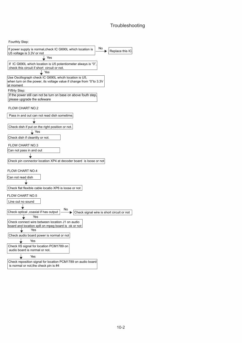
Fourthly Step:
FLOW CHART NO.2
FLOW CHART NO.3
FLOW CHART NO.4
FLOW CHART NO.5
Pass in and out can not read dish sometime.
Can not read dish
Line out no sound
Can not pass in and out
Check dish if put on the right position or not.
Check pin connector location XP4 at decoder board is loose or not
Check flat flexible cable locatio XP6 is loose or not
Check optical ,coaxial if has output
Check dish if cleanlily or not.
Fifthly Step:
If power supply is normal,check IC G690L which location is U5 voltage is 3.3V or not
If IC G690L which location is U5 potentiometer always is “0”,check this circuit if short circuit or not.
Use Oscillograph check IC G690L whcih location is U5,when turn on the power, its voltage value if change from “0”to 3.3V at moment
Replace this IC.
If the power still can not be turn on base on above fouth step, please upgrade the sofeware
Yes
Yes
Yes
Yes
Yes
Yes
No
NoCheck signal wire is short circuit or not
Check audio board power is normal or not
Check IIS signal for location PCM1789 on audio board is normal or not.
YesCheck reposition signal for location PCM1789 on audio board is normal or not,the check pin is #4
Check connect wire between location J1 on audio board and location xp8 on mpeg board is ok or not
Troubleshooting
10-2

Software Upgrading Procedure
1, Download the Software from Philips support Website:
2, Copy the Software upgrade file into USB device.
http://www.philips.com/support.
A, Connect to TV and Turn on Main Unit, D, When Software Upgrading finish,TV screendisplay
Software Upgrade finish.
Select Upgrad from USB,TV Screen Display:
TV Screen Display:
Press OK on Remote Control,TV Screen Display:
B, Press OK on Remote Control,
C, Software Upgrading
11-1

Software Version Check
1, Select the “IFO”, like below show:
2, TV Screen Display,select Version Info.
3, Select OK to get the Version information :
4, Press BACK on Remote Control:
TV Screen display:
5, Press 8-5-2-0 on Remote Control,can find Software Version:
12-1
B

MP
EGM
T853
0
DD
RII
DD
RII
KEY
IR
MC
UR
5F21
266
AC
YU
V
HD
MI
USB
USB
OPT
ICAL
CO
AXIA
L
VFD
Driv
erPT
1631
2
DD
RII
DD
RII
NAN
D-F
LASH
1G 1G 512M
512M
8G
Ethe
rnet
Ethe
rnet
YU
V
CVB
S
CEC
Col
limat
orII
FLAS
H1M
SMSC
8700
I2C
bus
Touc
hke
yx
3
DAC
CS4
352
DAC
CS4
352
DAC
CS4
352
DAC
CS4
352
7.1C
HAu
dio
OU
T
DAC
AK43
96
S/Pd
ifVF
DD
ispl
ay
40W
PSU
Load
er
MPE
G
Dis
play
MC
U5V
Reg
ulat
or
Tran
sfor
mer
2
Tran
sfor
mer
1
Touc
hed
key
WT5
700
OP
NE5
532
CVB
SLt
/Rt
POW
318C
Buffe
rFM
S636
3CS
WIF
IDO
NG
LEW
IFID
ON
GLE
CEC
ESD
REJ
ECTO
R
Mot
orD
river
R2A
3020
9SP
TPC
1391
G4
TRAY
IN/O
UT
A+A-
B+B-
UV
WC
OM
LOAD
+-
VFD
_BU
S
IR
CEC
Buf
fer
IN OU
T
BD
RO
MAS
A
AABB
UVW
C
TRV4
12VH
5
Bloc
k D
iagr
am
13-1
13-1
A+A-
B+B-
UV
WC
OM

Pow
er B
oard
MC
U5V
GN
DE
CO
-PO
WE
RG
ND
VF1
MC
U5V
VF2
-30V GN
DG
ND
EC
O-P
OW
ER
GN
D
K3
K2
GN
D
GN
DIR K
EY
_STB
YLE
D_S
TBY
EC
O_P
OW
ER
LED
Boa
rd
MC
U5V
DAT
AC
LK STB
K1K0
HP
D
STB CLK
GN
DH
DM
I5V
DAT
A
MU
TER
ST
CE
CG
ND
VC
C
GN
DG
ND
D+
D-
A+ B-
OP
U
B+
A-
+12V
+12V
1.0/
5P
GN
D-1
2V+5
V
GN
DG
ND
Blu
-Ray
Loa
der D
river
+5V
A+ B-
B+
A-
GN
D
NC
VC
C5V
GN
D
D+1
2V
D-1
2VG
ND
GN
D
AD
SD
ATA
0
AD
SD
ATA
1A
DS
DAT
A2
AC
BC
K
AD
SD
ATA
4
I/0A_M
UTE
AD
SD
ATA
3A
DM
CLK
GN
DA
DLR
CK
GN
D
NC
1.0/
24P
2.0/
5P1.
0/24
P SC
LS
DA
GN
D
VC
C
GN
DG
ND
2.0/
8P
Dec
oder
Boa
rd
D+D-
GND
3.3VRXDTXD
U CO
MWV
U CO
MWV
GND
3.3VRXDTXD
LOA
D+
2.O
/5P
1.O
/8P
2.O
/4P
2.O
/14P
2.O
/4P
2.O
/4P
LOA
D-
TRAY
+TR
AY-
GN
D
IR SC
LS
DA
DAT
A
1.0/
5PM
CU
Boa
rd
2.0/
14P
2.0/
13P
2.0/
5P
1.0/
5P
GN
D3.
3V
Touc
h B
oard
CLK
GN
DA
5V GN
D
VFD
Dis
play
Boa
rd
2.0/
10P
2.0/
14P
2.0/
2PLE
D+
LED
-
2.0/
5P2.
0/6P
2.5/
4P
2.5/
7P
12V
GN
DG
ND
5V
+5V+5VGND
GNDGND+12V-12V
AC
INP
UT
90--
250V
/50-
60H
Z
Pow
er C
ord
Wiri
ng D
iagr
am
14-1
14-1

Mai
n U
nit--
MC
U B
oard
Circ
uit D
iagr
am
15-1
15-1
D10
2
IN60
D10
3
IN60
IR_M
TK
IR_M
CU
C11
210
3
R11
110
K
MC
U+3
.3V
C11
510
4
R122680
IR_M
CU
R126100
CEC_INCEC_OUT
Q10
1BC
847B
R11
622
0
R10
2
100K
R10
4
47K
R10
527
KR
101
18K
C10
110
P
C10
2N
C/1
0PD
101
IN58
19C
ECA
CEC
3.3V
CEC
_OU
T
CEC
_IN
MC
U+3
.3V
L101
10uH
R12
110
0
R120100
R10
722
KR
108
22K
MC
U+3
.3V
I2C_SDAI2C_SCL
R123330MUTE
ECO_POWER
L103
10uH
MC
U+5
VM
CU
+3.3
V
C10
310
4
Q10
280
50
R11
722
0/1K
DZ1
013.
9V/3
K3C
E103
100u
/10
CE1
0110
0u/1
0C
105
104
R1242K2
LED_T1LED_T2LED_T3
LED_T1R11
347
LED
102
LED
W
LED_T2R11
447
LED
103
LED
W
LED_T3R11
547
MC
U+3
.3V
LED
104
LED
W
1234C
N10
2
2.0/
4P
RST
_MC
U1
MTK_RST
HPD
I2C
_SD
AI2
C_S
CL
GN
DH
DM
I+5V
MU
TE
GN
D
VFD
_CLK
VFD
_DAT
A
VFD
_STB
KEY_STBY
1234567891011121314CN
103
2.0/
14PM
CU
+5V
KEY_
STBY
GN
D
IR LED
_STB
YEC
O_P
OW
ER
VFD
_CLK
VFD
_DAT
A
VFD
_STB
CEC
A
MTK
_RST
IR_M
TK
P3.5
/SC
L1
P3.7
2R
ESET
3XO
UT
4VS
S5
XIN
6VC
C7
MO
DE
8
P4.5/INT0 9P1.7/INT1 10P3.6 11P3.1 12P5.4 13P5.3 14P1.6 15P1.5/RXD0 16P1
.4/T
XD0
17P1
.318
P1.2
19VR
EF20
P1.1
21P1
.022
P3.3
23P3
.4/S
DA
24
P0.725 P0.626 P0.527 P0.428 P0.3/AN429 P0.2/AN530 P0.1/AN631 P0.032
U10
1
R5F
2126
6NFP
R10
64K
7
MC
U+3
.3V
MC
U+3
.3V
R13
110
KMC
U+3
.3V
1 2 3 4 5 6 7 8 9 10 11 12 13CN
105
2.0/
13P
1 2 3 4 5CN
104
1.0/
5P
GN
DKE
Y_D
ATA
KEY_
CLK
R119100
JP10
20
JP10
30
JP10
50
JP10
60
JP10
80
MC
U+3
.3V
MC
U+3
.3V
JP10
90
P3.5
/SC
L
SDA_
MC
UI2
C_S
CL
I2C
_SC
L
CEC
_IN
CEC
_OU
T
C10
810
4
C11947PC12047P
I2C_SDA
I2C_SCL
JP10
70
GN
D
KEY
SW2
KEYSW0KEYSW1
K_SW
2
GN
D
KEYSW3
C113104C116104C104104C114104
MC
U+3
.3V
R10
922
KMC
U+3
.3V
TKEY
+3.3
VG
ND
KEY_
DAT
AKE
Y_C
LK
R1301K HPD
RST
_MC
U
GN
DM
CU
+3.3
V
MO
DE
L102
10uH
C10
710
4
L104
NC
/10u
H
_5V
JP11
00
MO
DE
JP11
10
GN
D
C106104
LED_STBYR125100
R11
022
K
MC
U+3
.3V
R11
222
K
KEY
SW0
KEY
SW1
KEY
SW2
KEY
SW3
_5V
IR
GN
D
JP11
20
LED
_T1
R11
8
100
TOD
ECO
DER
BOAR
D
SDA_
MC
U
JP10
10
JP10
40
C12
110
4
C12
247
PC
123
47P
KEY_DATA
KEY_CLK
C12447PC12547PC12647P
VFD_CLK
VFD_DATA
VFD_STB
C127104C128104
MUTE
MTK_RST
MC
U+3
.3V
R13
222
K
C12
910
3
L105
FB
L106
FBTK
_DAT
A
TK_C
LK
JP11
30
GN
D
C13
010
4C
131
104
C13
210
4
MAX
220P
F

Mai
n U
nit--
MC
U B
oard
Lay
out D
iagr
am
15-2
15-2
TOP
Layo
ut
Bot
tom
Lay
out

SW0
1SW
12
SW2
3SW
34
DO
5D
I6
VSS
7C
LK8
CS
9K0
10K1
11
K2 12K3 13VDD 14S0/K0 15S1/K1 16S2/K2 17S3/K3 18S4/K4 19S5/K5 20S6 21S7 22
S823
S924
S10
25S1
1/G
1026
VEE
27S1
2/G
928
S13/
G8
29S1
4/G
730
S15/
G6
31G
532
G4
33
G334 G235 G136 G037 VDD38 LED339 LED240 LED141 LED042 VSS43 OSC44
U20
1P
T631
2
R21
247
K
S1S2S3S4S5S6S7S8
S9S10
S11
G1
G2
G3
G4
G6
G5
DS-
DAT
DS-
CLK
DS-
STB
R20
5
2.2
1/2
SW
201
SW
H=5
.0
A5V
VFD
_CLK
VFD
_DAT
A
VFD
_STB
R22
247
123
IR20
1
+C
E20
3
100u
/10
R20
4
2.2
1/2
R21
7
4K7
MC
U+5
V
VFD
1VF
D2
R20
847
0R20
747
0
R20
647
0
R21110KR21010KR20910K
CE
201
100u
/10V
IRVC
C
VF1 1VF1 2
VF2 31VF2 32
NC 4S15 5S14 6NC 7S13 8S12 9S11 10S10 11S9 12S8 13S7 14S6 15S5 16S4 17S3 18S2 19S1 20NC 21G1 22G2 23G3 24G4 25G5 26G6 27G7 28G8 29
VFD
201
2007
5-2A
23
C20
610
4
S12
S13
S14
G7
G8
12345678910CN
201
2.0/
10P
GN
D
-30V
GN
DM
CU
+5V
VF_1
VF_2
12CN
203
2.0/
2PQ
201
8050
R21
815
0MC
U+5
V
LED_MID
LED
_MID
1 2 3 4 5 6 7 8 9 10 11 12 13 14CN
202
2.0/
14P
MC
U+5
V
KEY_
STBY
GN
DG
ND
IR LED
_STB
YEC
O_P
OW
ER
VFD
_CLK
VFD
_DAT
A
VFD
_STB
C21
010
4
R22
0
22K
MC
U+5
V
C207104
C21
610
4
C20
510
4
R22
1
4K7
Q20
2
8050
R21
91K
MC
U+5
V
LED
201
LED
RED
C21
110
4
LED
_MID
+LE
D_M
ID-
ECO
_PO
WER
A5V
C20
210
1
KEY_
STBY
MCU+5V
R22
333
IR
Mai
n U
nit -
-VFD
Dis
play
Boa
rd C
ircui
t Dia
gram
16-1
16-1
C20
3
104
-30V
CE202100u/10V
G1G2G3G4G5G6G7G8
S1
S2S3S4S5S6S7S8S9S10S11S12S13S14
VF1
VF2
VFD
1
VFD
2
-30V
C20
110
1
GN
D
GN
D
ECO_POWER
VF_2
JP20
50
VF_1
JP20
60
VF_2
JP20
70
A5V
JP20
80
JP20
90
JP21
00
JP21
10
JP21
20
JP21
30
-30V
GN
DVF
D2
VFD
2A5
VM
CU
+5V
KEY
SW0
KEY
SW1
KEY
SW2
KEY
SW3
KEY
SW0
KEY
SW1
KEY
SW2
KEY
SW3
C21
310
4A5V
C20
810
4C
209
104
MC
U+5
V C21
510
4
JP20
10
MC
U+5
VJP
202
0JP
203
0LE
D_M
ID1
IRIN
IRIN
LED
_STB
Y
VFD
_CLK
VFD
_DAT
A
VFD
_STB
R21
31K
R21
41K
R21
51K
R21
61K
KEY0
KEY1
KEY2
KEY3
MC
U+5
V
C21
410
4
C212104
C21747P
C21847P
VFD_CLK
VFD_DATA
GN
DJP
204
0
LED
_MID
1
JP21
40
ECO
_PO
WER
VF_1

Mai
n U
nit--
VFD
Dis
play
Boa
rd L
ayou
t Dia
gram
16-2
16-2
TOP
Layo
ut D
iagr
am
Bot
tom
Lay
out D
iagr
am

Mai
n U
nit--
Touc
h B
oard
Circ
uit &
Lay
out D
iagr
am
Circ
uit
Dia
gram
Top
Lay
out D
iagr
am
Bot
tom
Lay
out D
iagr
am
17-1
17-1
K1 K2 K3
12345
J801
1.0/
5P
GN
DKE
Y_D
ATA
KEY_
CLK
TKEY
+3.3
VG
ND
VDD
1
SI[0
]2
SI[1
]3
SI[3
]4
SI[8
]5
SI[1
0]6
SI[1
1]7
VSS
8O
UT1
19
OU
T10
10O
UT8
11SD
A12
SCL
13O
UT3
14O
UT1
15O
UT0
16
U80
1
IC-W
T570
0-S
160
C80
3N
C/5
P
C80
2N
C/5
P
C80
1N
C/5
P
TKEY
+3.3
V
C80
5
104
R80
12M
C80
4
104
C80
6
NC
/10P
C80
7
NC
/10PR
802
1K
R80
31K
R80
410
KR
805
47K
TKEY
+3.3
V
KEY_
DAT
AKE
Y_C
LK
KEY1
KEY2
KEY3
OP
EN
/CLO
SE
PLA
Y
PA
US
E

serv
o
SER
VO
DR
BOM
0.8
x (1
+909
/2K)
= 1
.16V
Low
ES
R <
125
mO
HM
0.8
x (1
+2.6
1K/2
K) =
1.8
4VLo
w E
SR
<12
5 m
OH
M
RES
ET#
-12V
+12V 3.3V
5V_V
CC
5V_G
1.1V
_FB
1.8V
_FB
-12V
_IN
+12V
_IN
+12V
A
VDD
12V
+5V_
IN
+12V
_IN
V21D
DVV21
NAF
RES
ET_M
CU
_FB
6
RES
ET#
5,6,
10
NO
R-R
ESET
#5,
6,10
-12V
9
+12V
4,5,
12
3.3V
2,4,
5,6,
7,9,
10,1
15V
_VC
C4,
9,11
+12V
A9
VCC
_P
-12V
3.3V
_VC
C5V
_VC
C
VCC
3IO
_STB
3.3V
_VC
C5V
_VC
C3.
3V_V
CC
3.3V
_VC
C3.
3V_V
CC
D3.
3V
M3.
3V
A3.3
V
1.2V
A1.2
V
D1.
2V
+12V
+12V
_P
3.3V
1.2V
3.3V
VCC
1.1V
+12V
+12V
_P+1
2V_P
3.3V
5V_V
CC
FE_G
ND
VCC
VCC
_P
1.1V
VCC
_P
1.8V
1.1V
VCC
+12V
A
-12V
VCC
_P
+12V
_P
+12V
A
FB54
FB/0
805/
33R
/2A
L10
TC50
26B#
470M
-U0-
B-47
uH-3
A
C13
NS/
100n
F
R20
0
D1
SK34
R14
100K
U1
AP11
22D
LSO
T-22
3
1
23
4AD
J/G
ND
OU
TIN
OU
T1
C15 10
uF/1
0V
R31
10K
C21
0.01
uF
L450
0 oh
m
R26
1K
R27
49.9
K_1%
PWR
2C
ON
2P-2
.5
CO
N2.
54-21 2
R12
4.7K
FB52
FB/0
805/
600R
C70
0.1u
F/16
V
CB4
0.1u
F
C40 2.2u
F
C10
NS/
100n
F
C29
10uF
/10V
R41 N
C
C16
10uF
/10V
C94
20.
1uF
+C
E2 220u
F/6.
3V
D2
NC
/1N
4148
/SM
D
R43
1K
R13
100K
L5N
C/5
00 o
hm
R28
100K
C73
10uF
/080
5
FB2
0904
FB
100R
DIP
R29
10K
Q32
BT39
04
C69 0.1u
F/16
V
R51
20K
+C
E7220u
F/16
V
C33
NS/
100n
F
TP98
CB6
0.1u
F
+C
E15
220u
F/16
V
FB4
0904
FB
100R
DIP
TP97TP89
+C
E607
470u
F/16
R35
1K
PO
R
U5
G69
0L29
3T73
U
1
3
2 GND
RES
ET#VCC
L9TC
5026
B#47
0M-U
0-B-
47uH
-3A
PWR
1C
ON
8P-2
.5
CO
N2.
54-8
1 2 3 4 5 6 7 8
+C
E422
0uF/
10V
C20
0.01
uF
CB1
40.
1uF
R3
909R
-1%
R11
2K-1
%
L633
ohm
+C
E347
0uF/
16V
C1
0.1u
F
R6
4.7K
+
CE5
220u
F/16
V
R9
2.61
k-1%
R4
2K-1
%
+C
E10
220u
F/10
V
R32
47K
+C
E11
100u
F/16
V
P_M
2
2 3 4 5
9 8 7 6
1
2 3 4 5
9 8 7 6
1
FB3
FB/0
805
TP99
C19
0.1u
F/16
V
FB6
FB/0
805
C39
NS/
100n
F
R19
0
CB2
0.1u
F
U4
AP15
38/S
OP-
8SO
P8/S
MD
1
2
3456
78
FB
EN
OC
SET
Vcc
O/P
O/P
VssVss
C27
10uF
/10V
Q6
AO34
01
1
3 2
TP103
C14
10uF
/10V
L350
0 oh
m
C23
0.1u
F/16
V
R24
100K
CB7
0.1u
F
CB3
0.1u
F
CB1
0.1u
FFB
59FB
/080
5/60
0R
D30
5
NC
/ESD
0603
/SM
D
P_M
1
2 3 4 5
9 8 7 6
1
2 3 4 5
9 8 7 6
1
C30
0.1u
F/16
V
+C
E110
0uF/
10V
D3
SK34
C31
10uF
/10V
+C
E23
470u
F/16
V+
CE2
6
CD
263/
220u
F/16
V
R8
100K
+C
E21
470u
F/16
V
U2
AP15
38/S
OP-
8SO
P8/S
MD
1
2
3456
78
FB
EN
OC
SET
Vcc
O/P
O/P
VssVss
Q7
BT39
04
FB51
FB/0
805/
600R
U8
G10
84-3
.3TO
-263
-3
3
1
2 4IN
ADJ/GND
OU
Tou
tt
+C
E25
CD
263/
220u
F/16
V
+C
E810
0uF/
16v
Q31
AO34
01
1
32
CB5
0.1u
F
Q2
2N39
041
32
C2
0.1u
F
L150
0 oh
m
+C
E24
470u
F/16
V
R33 NC
/0
FB1
FB/0
805
U3
APL1
117-
3.3
1
23
ADJ/GND
OU
TIN
CB1
00.
1uF
C72
10uF
/080
5
FB53
FB/0
805/
33R
/2A
R42
10K
FB60
FB/0
805/
600R
U11
CEM
9435
ASO
P8/S
MD
1 2 3 45678
S S S GDDDD
R30
100K
CB1
5
0.1u
F
L733
ohm
R40
10K
FB5
FB/0
805
Mai
n U
nit--
Dec
oder
Boa
rd C
ircui
t Dia
gram
18-1
18-1

AV
DD
12_M
EM
PLL
A_TN
_MEM
PLL
RE
XTU
P
A_T
P_M
EMPL
L
AV
DD
12_M
EM
PLL
A_C
LK0#
A_C
LK1
A_C
LK1#
D_C
LK0#
A_C
LK0
A_T
P_M
EMPL
L
A_R
A9
A_R
A3
A_R
A7
A_R
A12
A_C
S#
A_R
A11
A_C
AS
#A
_RA
13
A_C
KE
A_W
E#
A_R
A10
A_B
A0
A_R
A0
A_R
A8
A_R
A2
A_R
A1
A_R
A6
A_R
A4
A_R
AS
#A
_OD
T
A_B
A1
A_B
A2
A_R
A5
A_D
Q2
A_D
Q1
A_D
Q5
A_D
Q4
A_D
Q0
A_D
Q3
A_D
Q9
A_D
Q11
A_D
Q7
A_D
Q10
A_D
Q6
A_D
Q8
A_D
Q15
A_D
Q17
A_D
Q13
A_D
Q16
A_D
Q12
A_D
Q14
A_D
Q21
A_D
Q23
A_D
Q19
A_D
Q22
A_D
Q18
A_D
Q20
A_D
Q27
A_D
Q29
A_D
Q25
A_D
Q28
A_D
Q24
A_D
Q26
A_D
Q30
A_D
Q31
A_D
QM
0A
_DQ
M1
A_D
QM
2A
_DQ
M3
A_D
QS
0#
A_D
QS
3#
A_D
QS
1#A
_DQ
S2#
A_D
QS
1
A_D
QS
3A
_DQ
S2
A_D
QS
0
A_B
A1
A_B
A0
A_B
A2
A_C
AS
#A
_OD
T
A_C
S#
A_R
AS
#A
_WE
#A
_CK
E
A_R
A0
A_R
A1
A_R
A2
A_R
A3
A_R
A4
A_R
A5
A_R
A9
A_R
A10
A_R
A7
A_R
A11
A_R
A8
A_R
A6
A_R
A12
A_R
A13
A_C
LK0
A_C
LK0#
A_C
LK1
A_C
LK1#
A_TN
_MEM
PLL
A_B
A1
A_D
Q21
A_D
Q26
A_D
Q28
A_R
A8
A_D
QM
0
A_D
Q1
A_R
A6
A_C
KE
A_D
Q23
A_D
Q9
A_D
Q12
A_R
A4
A_O
DT
A_D
Q18
A_D
QS
2#
A_R
A13
A_R
A13
D_C
LK1
A_W
E#
A_R
A5
A_R
A2
A_B
A0
A_W
E#
A_D
Q16
A_D
QS
3
A_D
Q30
A_R
A7
A_C
S#
A_B
A2
A_D
Q5
A_D
QS
0#
A_R
A3
A_D
Q11
A_D
QS
1#
A_D
Q29
A_D
Q24
A_D
Q27
A_R
A4
A_R
A1
D_C
LK0
DD
R_V
RE
F
A_R
A11
A_R
A9
A_R
A7
A_R
AS
#
A_R
A5
A_R
A2
A_R
A10
A_D
Q13
A_D
Q3
D_C
LK1
A_D
QM
3
A_R
A3
A_R
AS
#
A_D
Q0
A_D
QS
0
A_R
A8
A_R
A0
A_D
Q25
A_R
A12
A_R
A6
A_O
DT
D_C
LK0#
A_D
Q15
A_D
QS
1
D_C
LK1#
DD
R_V
RE
F
A_B
A2
A_D
QS
2
A_R
A9
A_C
AS
#
A_B
A1
A_D
Q7
A_C
AS
#
A_D
Q19
A_D
Q20
A_D
Q31
A_D
Q10
A_D
Q2
A_D
Q22
A_D
Q17
A_B
A0
DD
R_V
RE
F
A_D
Q14
A_D
QM
1
A_D
Q6
DD
R_V
RE
F
A_R
A10
A_C
S#
A_D
QM
2
A_C
KE
A_D
Q8
DD
R_V
RE
F
A_R
A12
A_R
A1
D_C
LK1#
A_D
QS
3#
A_R
A11
A_D
Q4
A_R
A0
D_C
LK0
3.3V
3.3V
1,4,
5,6,
7,9,
10,1
1
1.2V
1.8V
1.8V
D0V
9D
0V9
3.3V
1.8V
1.8V
DD
R_V
RE
F
D0V
9
1.8V
1.8V
1.8V
1.8V
1.8V
1.8V
C11
10.
1uF/
16V
C10
70.
1uF/
16V
C12
60.
1uF/
16V
C13
2
0.1u
F/16
V04
02-C
C15
10.
1uF/
16V
0402
-C
C13
7
0.1u
F/16
V
C11
7
0.1u
F/16
V
0603
-C
C12
30.
1uF/
16V
C14
40.
1uF/
16V
FB10
00 06
03-L
C14
80.
1uF/
16V
R10
50
RN
101
100x
4
0402
-RP
8
18
27
36
45
R10
410
0 R10
810
006
03-R
R10
20
R10
0
100
C10
60.
1uF/
16V
R10
30
C13
6
0.1u
F/16
V
RN
100
100x
4
0402
-RP
8
18
27
36
45
C11
30.
1uF/
16V
C12
0
0.1u
F/16
V04
02-C
C14
00.
1uF/
16V
C12
40.
1uF/
16V
C13
1
0.1u
F/16
V04
02-C
C11
9
0.1u
F/16
V 0402
-C
C11
20.
1uF/
16V
C12
20.
1uF/
16V
C10
0
0.1u
F/16
V04
02-C
TP10
2
C12
94.
7uF
0805
-C
U10
2
64M
b x1
6 D
DR
2/10
66 F
BG
A 8
4FB
GA
84/S
MD
A1
A2
A3
A7
A8
A9
B1
B2
B3
B7
B8
B9
C1
C2
C3
C7
C8
C9
D1
D2
D3
D7
D8
D9
E1
E2
E3
E7
E8
E9F1
F2
F3F7
F8
F9 G1
G2
G7
G8
G9
H1
H2
H3
H7
H8
H9 J1J2
J3 J7J8
J9K2
K3
K7
K8
K9
L1L2 L3 L7L8M2
M3
M7
M8
M9
N1
N2
N3
N7
N8
P2
P3
P7
P8
P9
R1
R2
R3
R7
R8
G3
VD
D
NC
VS
SV
SS
Q
UD
QS
VD
DQ
DQ
14
VS
SQ
UD
M
UD
QS
VS
SQ
DQ
15
VD
DQ
DQ
9
VD
DQ
VD
DQ
DQ
8
VD
DQ
DQ
12
VS
SQ
DQ
11D
Q10
VS
SQ
DQ
13
VD
D
NC
VS
SV
SS
Q
LDQ
S
VD
DQ
DQ
6
VS
SQ
LDM
LDQ
S
VS
SQ
DQ
7
VD
DQ
DQ
1
VD
DQ
DQ
0
VD
DQ
DQ
4
VS
SQ
DQ
3D
Q2
VS
SQ
DQ
5
VD
DL
VR
EF
VS
SV
SS
DL
CK
VD
D
CK
EW
ER
AS
CK
OD
T
NC
/BA
2
BA
0B
A1
CA
SC
S
A10
/APA1
A2
A0
VD
DV
SSA3
A5
A6
A4
A7
A9
A11A8
VS
SV
DD
A12
NC
/A14
NC
/N15
NC
/A13
VD
DQ
C15
20.
1uF/
16V
0402
-C
C13
3
0.1u
F/16
V
C14
60.
1uF/
16V
C10
50.
1uF/
16V
C13
0
4.7u
F08
05-C
C11
00.
1uF/
16V
RN
103
100x
4
0402
-RP
8
18
27
36
45
C10
40.
1uF/
16V
C14
90.
1uF/
16V
C11
40.
1uF/
16V
R10
610
006
03-R
C15
4N
C08
05-C
C14
70.
1uF/
16V
C13
5
0.1u
F/16
V
R10
7N
C06
03-R
R10
10
C11
60.
1uF/
16V
C14
20.
1uF/
16V
C10
8
0.1u
F/16
V06
03-C
C14
30.
1uF/
16V
C10
52
22uF
/10v
TP10
0
C10
30.
1uF/
16V
C11
50.
1uF/
16V
RN
104
100x
4
0402
-RP
8
18
27
36
45
TP10
1
C13
4
0.1u
F/16
V
RN
105
100x
4
0402
-RP
8
18
27
36
45
C12
50.
1uF/
16V
U10
0AM
T853
0_D
DR
2M
T853
0/B
GA
702/
P0.
695/
B0.
5
AY
14B
B14
AY
30B
B30
AR
31A
Y34
BB
34W
35A
L35
AY
38B
B38
P40
V40
AB
40A
F40
AK
40A
P40
AV
40P
42V
42A
B42
AF4
2A
K42
AP
42A
V42
BB
42B
A43
AY
18B
B18
AV
16A
W15
BC
13A
U15
BA
13A
T16
BA
15B
C15
AY
20A
U19
BB
20A
T20
AW
19B
C19
AV
20B
A19
AV
32B
B32
AW
31B
C31
BA
31A
U31
AY
32A
T32
AY
36A
V36
BA
37A
U37
AW
35B
C37
AV
38B
B36
AT1
8A
V18
AV
34A
U35
BB
16B
A17
BC
33B
A35
AY
16B
C17
BA
33B
C35
BB
28A
U27
AT2
8
AW
23A
U23
AV
24B
B24
BC
29B
A29
BC
23A
T26
AV
26B
C27
AY
24A
V28
BC
25B
A27
BA
23A
W27
AY
28A
T24
BA
25A
V22
BC
21B
A21
BA
39B
C39
AV
30B
C43
AT3
0
AR
19A
Y22
BB
22
AY
26B
B26
AW
39A
Y40
BB
40B
C41
VC
C2I
OV
CC
2IO
VC
C2I
OV
CC
2IO
VC
C2I
OV
CC
2IO
VC
C2I
OV
CC
2IO
VC
C2I
OV
CC
2IO
VC
C2I
OV
CC
2IO
VC
C2I
OV
CC
2IO
VC
C2I
OV
CC
2IO
VC
C2I
OV
CC
2IO
VC
C2I
OV
CC
2IO
VC
C2I
OV
CC
2IO
VC
C2I
OV
CC
2IO
VC
C2I
OV
CC
2IO
VC
C2I
O
VC
C2I
OV
CC
2IO
A_D
Q0
A_D
Q1
A_D
Q2
A_D
Q3
A_D
Q4
A_D
Q5
A_D
Q6
A_D
Q7
A_D
Q8
A_D
Q9
A_D
Q10
A_D
Q11
A_D
Q12
A_D
Q13
A_D
Q14
A_D
Q15
A_D
Q16
A_D
Q17
A_D
Q18
A_D
Q19
A_D
Q20
A_D
Q21
A_D
Q22
A_D
Q23
A_D
Q24
A_D
Q25
A_D
Q26
A_D
Q27
A_D
Q28
A_D
Q29
A_D
Q30
A_D
Q31
A_D
QM
0A
_DQ
M1
A_D
QM
2A
_DQ
M3
A_D
QS
0#A
_DQ
S1#
A_D
QS
2#A
_DQ
S3#
A_D
QS
0A
_DQ
S1
A_D
QS
2A
_DQ
S3
A_B
A0
A_B
A1
A_B
A2
A_O
DT
A_C
AS
#A
_CS
#A
_RA
S#
A_W
E#
A_C
KE
A_R
A0
A_R
A1
A_R
A2
A_R
A3
A_R
A4
A_R
A5
A_R
A6
A_R
A7
A_R
A8
A_R
A9
A_R
A10
A_R
A11
A_R
A12
A_R
A13
A_R
CLK
0A
_RC
LK0#
A_R
CLK
1A
_RC
LK1# NC
A_R
EX
TDN
A_R
VR
EF
VC
C2I
OV
CC
2IO
VC
C2I
O
VC
C2I
OV
CC
2IO
A_A
VD
D12
_ME
MP
LLA
_AV
SS
12_M
EM
PLL
A_T
P_M
EM
PLL
A_T
N_M
EM
PLL
C12
80.
1uF/
16V
C12
70.
1uF/
16V
U10
3
G29
92B
T11U
2 154
3
VC
NTL
GN
DV
RE
F
VO
UT
VIN
C13
90.
1uF/
16V
C14
50.
1uF/
16V
U10
1
64M
b x1
6 D
DR
2/10
66 F
BG
A 8
4FB
GA
84/S
MD
A1
A2
A3
A7
A8
A9
B1
B2
B3
B7
B8
B9
C1
C2
C3
C7
C8
C9
D1
D2
D3
D7
D8
D9
E1
E2
E3
E7
E8
E9F1
F2
F3F7
F8
F9 G1
G2
G7
G8
G9
H1
H2
H3
H7
H8
H9 J1J2
J3 J7J8
J9K2
K3
K7
K8
K9
L1L2 L3 L7L8M2
M3
M7
M8
M9
N1
N2
N3
N7
N8
P2
P3
P7
P8
P9
R1
R2
R3
R7
R8
G3
VD
D
NC
VS
SV
SS
Q
UD
QS
VD
DQ
DQ
14
VS
SQ
UD
M
UD
QS
VS
SQ
DQ
15
VD
DQ
DQ
9
VD
DQ
VD
DQ
DQ
8
VD
DQ
DQ
12
VS
SQ
DQ
11D
Q10
VS
SQ
DQ
13
VD
D
NC
VS
SV
SS
Q
LDQ
S
VD
DQ
DQ
6
VS
SQ
LDM
LDQ
S
VS
SQ
DQ
7
VD
DQ
DQ
1
VD
DQ
DQ
0
VD
DQ
DQ
4
VS
SQ
DQ
3D
Q2
VS
SQ
DQ
5
VD
DL
VR
EF
VS
SV
SS
DL
CK
VD
D
CK
EW
ER
AS
CK
OD
T
NC
/BA
2
BA
0B
A1
CA
SC
S
A10
/APA1
A2
A0
VD
DV
SSA3
A5
A6
A4
A7
A9
A11A8
VS
SV
DD
A12
NC
/A14
NC
/N15
NC
/A13
VD
DQ
C10
10.
1uF/
16V
C13
80.
1uF/
16V
C15
60.
1uF/
16V
0603
-C
C12
10.
1uF/
16V
C10
9
0.1u
F/16
V04
02-C
C15
30.
1uF/
16V
R10
910
0
C10
20.
1uF/
16V
C11
8
0.1u
F/16
V
RN
102
100x
4
0402
-RP
8
18
27
36
45
C15
50.
1uF/
16V
0402
-C
C14
10.
1uF/
16V
C15
00.
1uF/
16V
Mai
n U
nit--
Dec
oder
Boa
rd C
ircui
t Dia
gram
18-2
18-2

RE
XTU
NB
_OD
TB
_OD
T
B_B
A0
B_R
A1
D_C
LK2#
B_R
A7
B_R
A2
B_R
A12
B_D
QS
1#
B_C
AS
#
B_R
A1
B_D
QS
2#
B_R
A10
B_W
E#
B_D
QS
1
DD
R_V
RE
FD
DR
_VR
EF
B_R
A7
B_R
A11
B_D
QM
1
B_B
A2
B_D
QS
2
B_R
A3
B_R
A9
B_R
A0
B_R
A2
B_B
A0
B_D
QS
0B
_DQ
S0#
B_C
KE
B_R
A9
B_C
S#
B_R
A10
D_C
LK3
D_C
LK2
B_D
QM
2
B_B
A2
B_R
A4
B_R
A11
B_R
A6
B_R
A12
B_C
S#
B_O
DT
B_B
A1
B_D
QS
3
B_R
A6
B_D
QM
0B
_OD
T
B_R
A5
B_R
AS
#
B_D
QM
3
B_R
A8
B_R
A13
D_C
LK3#
B_C
AS
#
B_B
A1
B_R
A4
B_D
QS
3#
B_W
E#
B_R
A5
B_R
A8
B_R
AS
#
B_R
A13
B_R
A3
B_C
KE
B_R
A0
2KL
C_D
0KL
C_B B
_CLK
1
#2KL
C_D
#0KL
C_B
D_C
LK3#
D_C
LK3
B_C
LK1#
B_D
QM
0
B_D
QM
2B
_DQ
M3
B_D
QM
1
B_D
QS
3#
B_D
QS
1#B
_DQ
S0#
B_D
QS
2#
B_D
QS
1
B_D
QS
3
B_D
QS
0
B_D
QS
2
B_B
A1
B_B
A0
B_B
A2
B_C
AS
#
B_W
E#
B_C
KE
B_R
AS
#B
_CS
#
B_R
A1
B_R
A0
B_R
A13
B_R
A3
B_C
LK1#
B_R
A7
B_R
A6
B_R
A4
B_R
A2
B_R
A5
B_R
A8
B_R
A9
B_R
A11
B_R
A10
B_C
LK1
B_R
A12
B_C
LK0#
B_C
LK0
B_D
Q17
B_D
Q13
B_D
Q12
B_D
Q18
B_D
Q16
B_D
Q11
B_D
Q0
B_D
Q3
B_D
Q2
B_D
Q1
B_D
Q4
B_D
Q6
B_D
Q5
B_D
Q7
B_D
Q8
B_D
Q9
B_D
Q10
B_D
Q14
B_D
Q15
B_D
Q19
B_D
Q21
B_D
Q20
B_D
Q23
B_D
Q22
B_D
Q24
B_D
Q25
B_D
Q26
B_D
Q27
B_D
Q28
B_D
Q29
B_D
Q30
B_D
Q31
B_D
Q4
B_D
Q6
B_D
Q7
B_D
Q10
B_D
Q14
B_D
Q11
B_D
Q13
B_D
Q0
B_D
Q1
B_D
Q15
B_D
Q9
B_D
Q12
B_D
Q3
B_D
Q5
B_D
Q8
B_D
Q2
B_D
Q25
B_D
Q27
B_D
Q28
B_D
Q19
B_D
Q21
B_D
Q17
B_D
Q18
B_D
Q30
B_D
Q24
B_D
Q23
B_D
Q29
B_D
Q26
B_D
Q22
B_D
Q20
B_D
Q16
B_D
Q31
B_R
A5
B_C
KE
B_B
A1
B_W
E#
B_B
A2
B_R
A9
B_R
A10
B_R
A7
B_B
A0
B_R
A12
B_C
S#
B_R
A1
B_O
DT
B_R
A0
B_R
A2
B_R
A8
B_R
A4
B_R
A6
B_R
A11
B_R
A13
B_R
AS
#
B_C
AS
#B
_RA
3
DD
R_V
RE
FD
DR
_VR
EF
DD
R_V
RE
F
DD
R_V
RE
F
DD
R_V
RE
F
1.8V
DD
R_V
RE
F
1.8V
1.8V
DD
R_V
RE
F
D0V
9
1.8V
1.8V
1.8V
1.8V
DD
R_V
RE
F
R20
110
0
C22
30.
1uF/
16V
TP20
0
C23
40.
1uF/
16V
C20
1
0.1u
F/16
V
C20
6
0.1u
F/16
V C21
9
0.1u
F/16
V
U20
1
64M
b x1
6 D
DR
2/10
66 F
BG
A 8
4FB
GA
84/S
MD
A1
A2
A3
A7
A8
A9
B1
B2
B3
B7
B8
B9
C1
C2
C3
C7
C8
C9
D1
D2
D3
D7
D8
D9
E1
E2
E3
E7
E8
E9F1
F2
F3F7
F8
F9 G1
G2
G7
G8
G9
H1
H2
H3
H7
H8
H9 J1J2
J3 J7J8
J9K2
K3
K7
K8
K9
L1L2 L3 L7L8M2
M3
M7
M8
M9
N1
N2
N3
N7
N8
P2
P3
P7
P8
P9
R1
R2
R3
R7
R8
G3
VD
D
NC
VS
SV
SS
Q
UD
QS
VD
DQ
DQ
14
VS
SQ
UD
M
UD
QS
VS
SQ
DQ
15
VD
DQ
DQ
9
VD
DQ
VD
DQ
DQ
8
VD
DQ
DQ
12
VS
SQ
DQ
11D
Q10
VS
SQ
DQ
13
VD
D
NC
VS
SV
SS
Q
LDQ
S
VD
DQ
DQ
6
VS
SQ
LDM
LDQ
S
VS
SQ
DQ
7
VD
DQ
DQ
1
VD
DQ
DQ
0
VD
DQ
DQ
4
VS
SQ
DQ
3D
Q2
VS
SQ
DQ
5
VD
DL
VR
EF
VS
SV
SS
DL
CK
VD
D
CK
EW
ER
AS
CK
OD
T
NC
/BA
2
BA
0B
A1
CA
SC
S
A10
/APA1
A2
A0
VD
DV
SSA3
A5
A6
A4
A7
A9
A11A
8
VS
SV
DD
A12
NC
/A14
NC
/N15
NC
/A13
VD
DQ
RN
203
100x
4
0402
-RP
8
18
27
36
45
C23
10.
1uF/
16V
C22
90.
1uF/
16V
C21
6
0.1u
F/16
V
C20
9
0.1u
F/16
V
C22
40.
1uF/
16V
C23
50.
1uF/
16V
C22
10.
1uF/
16V
C21
5
0.1u
F/16
V
C23
70.
1uF/
16V
C22
20.
1uF/
16V
R20
610
006
03-R
C20
00.
1uF/
16V
0603
-C
C21
4
0.1u
F/16
V
C21
7
0.1u
F/16
V
C21
0
0.1u
F/16
V
C22
6
0.1u
F/16
V
RN
200
100x
4
0402
-RP
8
18
27
36
45
RN
204
100x
4
0402
-RP
8
18
27
36
45
C20
7
0.1u
F/16
V
C23
30.
1uF/
16V
C21
8
0.1u
F/16
V
C20
4
0.1u
F/16
V
C20
8
0.1u
F/16
V
C23
20.
1uF/
16V
R20
50
C21
1
0.1u
F/16
V
C20
5
0.1u
F/16
V
C23
60.
1uF/
16V
C23
90.
1uF/
16V
0402
-C
C20
3
0.1u
F/16
V
C22
50.
1uF/
16V
C22
70.
1uF/
16V
C20
2
0.1u
F/16
V
C22
0
0.1u
F/16
V
C23
00.
1uF/
16V
R20
410
0
RN
202
100x
4
0402
-RP
8
18
27
36
45
RN
201
100x
4
0402
-RP
8
18
27
36
45
C22
80.
1uF/
16V
C21
2
0.1u
F/16
V
R20
30
R20
00
U10
0BM
T853
0_D
DR
2M
T853
0/B
GA
702/
P0.
695/
B0.
5
J9 J11
T12
V12
P12 J13
U13
W13
AW
13 T14
P14
AT1
4H
16A
R17
AU
17A
W17 J1
9A
A21
AC
21A
E21
AG
21A
J21
AU
21A
W21
Y22
AK
22A
T22
J23
AC
23A
E23
AG
23Y
24A
B24
AD
24A
F24
AH
24A
K24
AC
25A
E25
AG
25A
R25
AU
25A
W25
Y26
AB
26A
D26
AF2
6A
H26
AK
26A
C27
AE
27A
G27
Y28
AB
28A
D28
AF2
8A
H28
AK
28A
C29
AE
29A
G29
AR
29A
U29
AW
29Y
30A
K30
AA
31A
C31
AE
31A
G31
AJ3
1A
U33
AW
33A
T34
U35
AA
35A
E35
AJ3
5A
N35
H36
AT3
6G
37N
37U
37A
A37
AE
37A
J37
AN
37A
W37
N39
U39
AA
39A
E39
AJ3
9A
N39
AU
39B
A41
AY
42V
14 AJ7
AR
39A
W43
AU
43A
U41
AW
41A
T38
AR
37A
P36
AN
43A
K36
AM
40A
L37
AM
38A
M42
AL3
9A
N41
Y38
AA
41W
37A
A43
Y40
W39
Y42
Y36
T40
R37
R43
T38
T36
R41
R39
T42
AP
38A
M36
V38
V36
AT4
2A
R41
W43
U41
AT4
0A
R43
W41
U43
AD
40A
D36
AC
39
AH
40A
D42
AJ4
1A
C43
AC
41A
B38
AG
43A
F38
AG
37A
J43
AH
42A
C37
AG
39A
E43
AH
36A
D38
AF3
6A
H38
AE
41A
K38
AL4
3A
L41
N41
N43
AG
41M
42A
B36
U15
W15
Y14
K34
R35
DV
SS
DV
SS
DV
SS
DV
SS
DV
SS
DV
SS
DV
SS
DV
SS
DV
SS
DV
SS
DV
SS
DV
SS
DV
SS
DV
SS
DV
SS
DV
SS
DV
SS
DV
SS
DV
SS
DV
SS
DV
SS
DV
SS
DV
SS
DV
SS
DV
SS
DV
SS
DV
SS
DV
SS
DV
SS
DV
SS
DV
SS
DV
SS
DV
SS
DV
SS
DV
SS
DV
SS
DV
SS
DV
SS
DV
SS
DV
SS
DV
SS
DV
SS
DV
SS
DV
SS
DV
SS
DV
SS
DV
SS
DV
SS
DV
SS
DV
SS
DV
SS
DV
SS
DV
SS
DV
SS
DV
SS
DV
SS
DV
SS
DV
SS
DV
SS
DV
SS
DV
SS
DV
SS
DV
SS
DV
SS
DV
SS
DV
SS
DV
SS
DV
SS
DV
SS
DV
SS
DV
SS
DV
SS
DV
SS
DV
SS
DV
SS
DV
SS
DV
SS
DV
SS
DV
SS
DV
SS
DV
SS
DV
SS
DV
SS
DV
SS
DV
SS
DV
SS
DV
SS
DV
SS
DV
SS
DV
SS
DV
SS
DV
SS
DV
SS
DV
SS
DV
SS
DV
SS
DV
SS
DV
SS
DV
SS
DV
SS
_XTA
L
B_D
Q0
B_D
Q1
B_D
Q2
B_D
Q3
B_D
Q4
B_D
Q5
B_D
Q6
B_D
Q7
B_D
Q8
B_D
Q9
B_D
Q10
B_D
Q11
B_D
Q12
B_D
Q13
B_D
Q14
B_D
Q15
B_D
Q16
B_D
Q17
B_D
Q18
B_D
Q19
B_D
Q20
B_D
Q21
B_D
Q22
B_D
Q23
B_D
Q24
B_D
Q25
B_D
Q26
B_D
Q27
B_D
Q28
B_D
Q29
B_D
Q30
B_D
Q31
B_D
QM
0B
_DQ
M1
B_D
QM
2B
_DQ
M3
B_D
QS
0#B
_DQ
S1#
B_D
QS
2#B
_DQ
S3#
B_D
QS
0B
_DQ
S1
B_D
QS
2B
_DQ
S3
B_B
A0
B_B
A1
B_B
A2
B_C
AS
#B
_CS
#B
_RA
S#
B_W
E#
B_C
KE
NC
1
B_R
A0
B_R
A1
B_R
A2
B_R
A3
B_R
A4
B_R
A5
B_R
A6
B_R
A7
B_R
A8
B_R
A9
B_R
A10
B_R
A11
B_R
A12
B_R
A13
B_R
CLK
0B
_RC
LK0#
B_R
CLK
1B
_RC
LK1#
B_O
DT
B_R
EX
TDN
B_R
VR
EF
DV
SS
DV
SS
DV
SS
DV
SS
DV
SS
C23
80.
1uF/
16V
0603
-C
RN
205
100x
4
0402
-RP
8
18
27
36
45
U20
2
64M
b x1
6 D
DR
2/10
66 F
BG
A 8
4FB
GA
84/S
MD
A1
A2
A3
A7
A8
A9
B1
B2
B3
B7
B8
B9
C1
C2
C3
C7
C8
C9
D1
D2
D3
D7
D8
D9
E1
E2
E3
E7
E8
E9F1
F2
F3F7
F8
F9 G1
G2
G7
G8
G9
H1
H2
H3
H7
H8
H9 J1J2
J3 J7J8
J9K2
K3
K7
K8
K9
L1L2 L3 L7L8M2
M3
M7
M8
M9
N1
N2
N3
N7
N8
P2
P3
P7
P8
P9
R1
R2
R3
R7
R8
G3
VD
D
NC
VS
SV
SS
Q
UD
QS
VD
DQ
DQ
14
VS
SQ
UD
M
UD
QS
VS
SQ
DQ
15
VD
DQ
DQ
9
VD
DQ
VD
DQ
DQ
8
VD
DQ
DQ
12
VS
SQ
DQ
11D
Q10
VS
SQ
DQ
13
VD
D
NC
VS
SV
SS
Q
LDQ
S
VD
DQ
DQ
6
VS
SQ
LDM
LDQ
S
VS
SQ
DQ
7
VD
DQ
DQ
1
VD
DQ
DQ
0
VD
DQ
DQ
4
VS
SQ
DQ
3D
Q2
VS
SQ
DQ
5
VD
DL
VR
EF
VS
SV
SS
DL
CK
VD
D
CK
EW
ER
AS
CK
OD
T
NC
/BA
2
BA
0B
A1
CA
SC
S
A10
/APA1
A2
A0
VD
DV
SSA3
A5
A6
A4
A7
A9
A11A
8
VS
SV
DD
A12
NC
/A14
NC
/N15
NC
/A13
VD
DQ
R20
20
C21
3
0.1u
F/16
V
Mai
n U
nit--
Dec
oder
Boa
rd C
ircui
t Dia
gram 18
-318
-3
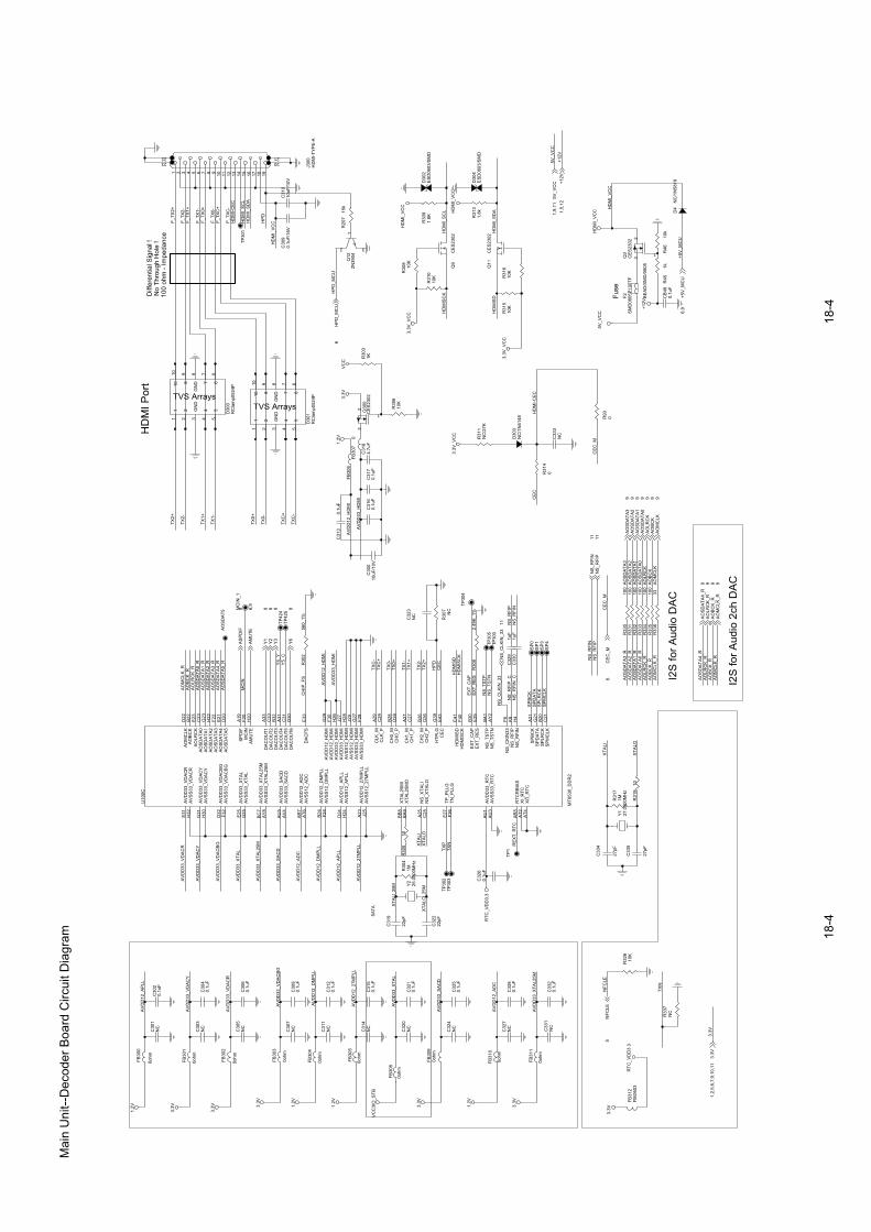
100
ohm
-Im
peda
nce
No
Thro
ugh
Hol
e!
HD
MI P
ort
Diff
eren
tialS
igna
l!
I2S
for A
udio
DA
C
I2S
for A
udio
2ch
DA
C
SATA
Fuse
HD
MI_
SD
A
HD
MI-C
EC
F_TX
0-
HP
D
F_TX
1+
HD
MI_
SC
L
CE
C
F_TX
C-
F_TX
C+
AV
DD
33_V
DA
CR
AV
DD
12_D
MP
LL
AV
DD
33_V
DA
CY
F_TX
2-
F_TX
2+
F_TX
1-F_
TX0+
HD
MI_
SC
L
HD
MI_
SD
A
AV
DD
12_A
PLL
AV
DD
12_2
7MP
LL
AVD
D33
_XTA
L
AV
DD
33_V
DA
CB
G
AV
DD
33_S
AC
D
AV
DD
12_A
DC
AVD
D33
_XTA
L25M
AV
DD
33_V
DA
CR
AV
DD
33_V
DA
CY
AV
DD
33_V
DA
CB
G
AVD
D33
_XTA
L TXP
TXNXTA
LOX
TALI
AV
DD
12_2
7MP
LL
AV
DD
12_A
PLL
AV
DD
12_D
MP
LL
AV
DD
12_A
DC
AV
DD
33_S
AC
D
AVD
D33
_XTA
L25M
NS
_RFI
N_C
PIFR_
SN
C_PIF
R_S
NN
S_R
FIN
NS
_TS
TNN
S_TS
TP
EXT_
RES
EXT_
CAP
HD
MIS
DH
DM
ISC
K
HP
DC
EC
TX2+
TX2-
TX1-
TX1+
TX0-
TX0+
TXC
+TX
C-
AV
DD
12_H
DM
I
AV
DD
33_H
DM
I
CH
IP_F
S
AO
LRC
K_R
AO
SD
ATA
3_R
AO
SD
ATA
1_R
AO
MC
LK_R
AO
SD
ATA
4_R
AO
BC
K_R
AO
SD
ATA
0_R
AO
SD
ATA
2_R
XTA
LI
XTA
LO
TXN
AV
DD
33_H
DM
I
AO
SD
ATA
2A
OS
DA
TA3
AO
LRC
K_R
AO
SD
ATA
1
AO
MC
LK
AO
LRC
KA
OB
CK
_R
AO
SD
ATA
3_R
AO
SD
ATA
0_R
AO
BC
KA
OM
CLK
_R
AO
SD
ATA
2_R
AO
SD
ATA
1_R
AO
SD
ATA
0
HD
MIS
D
HD
MIS
CK
AV
DD
12_H
DM
I
NFC
LE
NS
_RFI
PN
S_R
FIN
NS
_CLK
IN_3
3
REX
T_R
TC
TX2-
TX1-
TX0-
TXC
-
TXC
+
TX1+
TX2+
TX0+
XTAL
I_25
M
XTA
LO_2
5M
CE
C_M
CE
C_M
SP
DA
TA
SP
MC
LK
SP
BC
K
SP
LRC
K
Y4_
YY
5_C
AO
SD
ATA
4_R
AO
LRC
K_R
AO
MC
LK_R
AO
BC
K_R
AO
SD
ATA
5_R
MC
IN
3.3V
HD
MI-C
EC
5V_V
CC
HD
MI_
VC
C
HP
D_M
CU
+5V
_MC
U
HD
MI_
VC
C
+12V
Y1
8Y
28
Y6
8
Y3
8
AS
PD
IF8
AMU
TE6,
9
NS
_RFI
N11
NS
_RFI
P11
NFC
LE5
AO
SD
ATA
19
AO
BC
K9
AO
LRC
K9
AO
SD
ATA
39
AO
SD
ATA
09
AO
MC
LK9
AO
SD
ATA
29
NS
_CLK
IN_3
311
CE
C_M
6
AO
BC
K_R
9A
OLR
CK
_R9
AO
SD
ATA
4_R
9
AO
MC
LK_R
93.
3V1,
2,5,
6,7,
9,10
,11
5V_V
CC
1,9,
11
HP
D_M
CU
6
+5V
_MC
U6,
9
+12V
1,5,
12
3.3V
_VC
C
1.2V
3.3V
3.3V 3.
3V
1.2V
1.2V
VC
C3I
O_S
TB
3.3V
3.3V
_VC
C
3.3V
_VC
CH
DM
I_V
CC
HD
MI_
VC
C
1.2V
3.3V
RTC
_VD
D3.
3
3.3V
RTC
_VD
D3.
3
1.2V
3.3V
VC
C
5V_V
CC
HD
MI_
VC
C
+12V
C30
010
uF/1
0V
FB30
3
0ohm
D30
2E
SD
0603
/SM
D
Q12
2N39
041
32
C31
60.
1uF
R30
02.
49K
_1%
U10
0C
MT8
530_
DD
R2
E31
H32
G31
H30
D32 F3
2
E25
G25
BC
7A
Y8
AU
5A
V4
AR
7A
T6 B24 F2
4
D24
H24
A23 J2
5
BB
8B
A9
A25
C25
E27 F2
6
AU
1A
U3
AR
5A
T2A
T4
D22
B22
E23
C23
G23
H22
F22
E21
D20
A19
F20
H20
A33
C33
B32
A31
C31
D30
E33
G29
F30
H26
J27
H28
J29
G27
F28
A29
C29
B28
D28
A27
C27
B26
D26
G39
E43
E41
F40
B30
E29
BA
1A
Y2
F6 K8
H4
A21
G21
B20
C21
AV
DD
33_V
DA
CR
AV
SS
33_V
DA
CR
AV
DD
33_V
DA
CY
AV
SS
33_V
DA
CY
AV
DD
33_V
DA
CB
GA
VS
S33
_VD
AC
BG
AV
DD
33_X
TAL
AV
SS
33_X
TAL
AV
DD
33_X
TAL2
5MA
VS
S33
_XTA
L25M
AV
DD
33_S
AC
DA
VS
S33
_SA
CD
AV
DD
12_A
DC
AV
SS
12_A
DC
AV
DD
12_D
MP
LLA
VS
S12
_DM
PLL
AV
DD
12_A
PLL
AV
SS
12_A
PLL
AV
DD
12_2
7MP
LLA
VS
S12
_27M
PLL
XTA
L25M
IX
TAL2
5MO
NS
_XTA
LIN
S_X
TALO
TP_P
LLG
TN_P
LLG
AV
DD
33_R
TCA
VS
S33
_RTC
RTC
RB
IAS
XI_
RTC
XO
_RTC
AO
MC
LKA
OB
CK
AO
LRC
KA
OS
DA
TA0
AO
SD
ATA
1A
OS
DA
TA2
AO
SD
ATA
3A
OS
DA
TA4
AO
SD
ATA
5
SP
DIF
MC
INA
MU
TE
DA
CO
UT1
DA
CO
UT2
DA
CO
UT3
DA
CO
UT4
DA
CO
UT5
DA
CO
UT6
DA
CFS
AV
DD
12_H
DM
IA
VD
D12
_HD
MI
AV
DD
33_H
DM
IA
VD
D33
_HD
MI
AV
SS
12_H
DM
IA
VS
S12
_HD
MI
AV
SS
33_H
DM
IA
VS
S33
_HD
MI
CLK
_MC
LK_P
CH
0_M
CH
0_P
CH
1_M
CH
1_P
CH
2_M
CH
2_P
HTP
LGC
EC
HD
MIS
DH
DM
ISC
K
EX
T_C
AP
EX
T_R
ES
NS
_TS
TPN
S_T
STN
NS
_CK
IN33
NS
_RFI
PN
S_R
FIN
SP
BC
KS
PD
ATA
SP
LRC
KS
PM
CLK
R45
1k
FB30
1
0ohm
C30
1N
C
SP
1
C30
60.
1uF
FB31
1
0ohm
C30
90.
1uF/
16V
C32
91u
F
C31
50.
1uF
FB31
0
0ohm
R46
10k
FB30
5
0ohm
C33
01u
FD
303
NC
/1N
4148
C31
9
22pF
F2S
MD
0805
P10
0TF
BE
AD
/SM
D/0
805
TP30
5
C33
4
27pF
C31
84.
7uF
SP
3
R31
610
K
R30
610
K
C33
5
27pF
FB30
70
R33
010
0
TP30
1
C31
30.
1uF
R33
7N
C
R33
110
0
C33
20.
1uF
SP
4
FB30
8
0ohm
C30
7N
C
Q9
CE
S23
02
R30
810
K
R30
31K
R31
510
K
TP30
4
C30
3N
C
TP1
Q3
CE
S23
02
1
32
FB30
0
0ohm
Y2
25.0
000M
Hz
C31
010
uF/1
0V
C32
50.
1uF
C30
20.
1uF
C30
80.
1uF
R31
1N
C/2
7K
R30
256
0_1%
TVS Arrays
D30
0R
Cla
mp0
524P
1 2 3 4 5678910
1 2 GN
D
4 567
GN
D810
R31
010
K
AO
SD
AT5
C33
3N
C
Y1
27.0
000M
Hz
R31
71M
R30
41M
R32
610
K
D30
4E
SD
0603
/SM
D
TP30
0
SP
0
Q30
0C
ES
2302
1
23
C32
4N
C
D4
NC
/1N
5819
TP30
2
R93
0
R33
310
0
C31
70.
1uF
J300
HD
MI-T
YP
E-A
1 2 3 4 5 6 7 8 9 10 11 12 13 14 15 16 17 18 19
22 212023
R33
633
R33
510
0
C30
5N
C
C32
60.
1uF
C31
20.
1uF
CB
490.
1uF
C31
1N
C
TVS Arrays
D30
1R
Cla
mp0
524P
1 2 3 4 5678910
1 2 GN
D
4 567
GN
D810
C32
3N
C
TP42
4
C31
4N
C
FB30
4
0ohm
C32
10.
1uF
C32
0N
C
C32
80.
1uF
R33
210
0
R30
510
R33
410
0
Q11
CE
S23
02
FB31
2FB
/060
3
R30
91.
8K
FB30
6
FB30
2
0ohm
R31
40
R31
31.
8k
C32
7N
C
TP42
5
TP30
3
R20
715
k
MC
IN_1
FB30
90o
hm
R31
910
R30
7N
C
C32
222
pF
C33
1N
C
C30
40.
1uF
Mai
n U
nit--
Dec
oder
Boa
rd C
ircui
t Dia
gram 18
-418
-4

NA
ND
Fla
sh
SA
TA I/
F
FOR
WiF
i
SD C
ARD
I/F
Fuse
NFD
3
NFD
5
NFD
2N
FWE
NN
FALE
NFW
P#
NFD
4
NFD
7
NFD
1
NFR
EN
NFD
6
NFD
0
NFR
BN
NFC
LE
SATA
_TXP
1_C
SATA
_TXN
1_C
SA
TA_R
XN
1_C
SATA
_RXP
1_C
NFC
EN
2
US
FCS
#U
SFD
OU
SFC
K
US
FDI
NFC
EN
3
FES
FDI
NFD
4
US
BP
0
SATA
_RXP
2_C
US
FDO
NFD
0
MR
ESET
_
US
BM
1
GP
IO1
AV
DD
12_S
RX
2
GP
IO3
GP
IO2NFR
EN
FES
FDI
SFC
S
NFD
5
SATA
_TXP
2_C
US
BP
1
US
BM
0
SATA
_TXP
1_C
NFD
1
NFR
BN
SATA
_TXN
1_C
VC
LK25
MI
VD
D3.
3_U
SB
NFD
3
PA
D_V
RT
SR
EF
TTD
I
VD
D1.
2_U
SB
AV
DD
12_S
TX1
US
FCK
TTD
O
AV
DD
33_S
T
GP
IO6
SATA
_RXP
1_C
NFD
6
TTM
S
TTR
ST#
SVC
TST
NFC
EN
2
AV
DD
12_S
T
US
FCS
#
TTC
K
SD
A
US
FDI
GP
IO4NFA
LE
SC
L
NFC
LE
NFW
EN
SATA
_TXN
2_C
GP
IO7N
FCE
N
SA
TA_R
XN
2_C
GP
IO5
FES
FDO
AV
DD
12_S
RX
1
GP
IO0SFC
K
NFD
2
NFD
7
NFR
BN
2
FES
FCK
FES
FCS
SA
TA_R
XN
1_C
AV
DD
12_S
TX2
NFC
EN
NFR
BN
2
GP
IO7
NFC
EN
4_R
US
BM
0
US
BP
0U
SB
P0
US
BM
0
USB_OC0
U5V
0
US
BP
1U
SB
M1
U5V
0
SVC
TST
NO
R-R
ES
ET#
SFC
S
SATA
_RXP
2_C
SATA
_TXP
2_C
SA
TA_R
XN
2_C
SATA
_TXN
2_C
TTR
ST#
TTD
O
TTM
STT
CK
TTD
I
GP
IO3
GP
IO4
GP
IO2
GP
IO1
GP
IO0
GP
IO5
US
B_O
C1
HS
YN
C_I
N0
CO_
BS
UNI_
CN
YS
V
1N
E_B
SU
CN
YS
HTU
OV
US
B_E
N0
VO
UTV
SY
NC
3.3V
VO
UTC
LK2
VO
UTC
LK2
GP
IO6
EN
US
B_E
N0
US
BM
1
1P
BS
U1
PB
SU
US
BM
1
U5V
VC
C_U
SB
+12V
NO
R-R
ES
ET#
US
BM
0U
SB
P0
TRTC
K
TTR
ST#
TTD
O
TTM
STT
CK
TTD
I
TRTC
K
3.3V
SFC
K6
NFC
LE4
NFC
EN
6N
FALE
6
NFR
EN
6
NFC
EN
26
NFW
EN
6
SC
L6,9
SD
A6,9
RS
TI11
,12
25M
_Buf
11
US
FDO
11U
SFC
S#
11
US
FCK
11FE
SFD
I6
US
FDI
11
RX
IP11
RX
IN11
TXO
P11
TXO
N11
NO
R-R
ES
ET#
1,6,
10
DA
C_R
ST#
9
VS
YN
C_I
N7
HS
YN
C_I
N7
VO
UTV
SY
NC
7V
OU
THS
YN
C7
3.3V
1,2,
4,6,
7,9,
10,1
1
VO
UTC
LK2
7
+12V
1,4,
12
3.3V
3.3V
1.2V
1.2V
1.2V
3.3V
1.2V
3.3V
3.3V
VC
C
3.3V
VC
C
+12V
TP56
C36
9N
C
TP35
3
FB35
20o
hm
C36
80.
1uF
R35
410
K C35
80.
1uF/
16V
C36
2N
C
TP41
9
C35
30.
1uF
U35
1
NA
ND
08G
W3B
2A
1 2 3 4 5 6 7 8 9 10 11 12 13 14 15 16 17 18 19 20 21 22 23 24252627282930313233343536373839404142434445464748
NC
NC
NC
NC
NC SE
R/B RE
CE
NC
NC
VC
CV
SS
NC
NC
CLE
ALE WE
WP
NC
NC
NC
NC
NC
NC
NC
NC
NC
I/O0
I/O1
I/O2
I/O3
NC
NC
NC
VS
SV
CC
NC
NC
NC
I/O4
I/O5
I/O6
I/O7
NC
NC
NC
NC
SD
_CM
D_1
R36
233
R15
251
0
R10
53
NC
TVS Arrays
D35
1
RC
lam
p052
2P
1 2 3456
1 2 GN
DG
ND56
R37
90
FB35
10o
hm
R382NC
FB35
60o
hm
TP55
TP42
0
TP35
9
TOP
HA
2
NC
/HE
AD
ER
8 S
MD
1.0
TOP
CO
N1.
25-8
-SM
T-XP
12345678910
R13
8
24.9
K1%
C15
9
100N
F
USB-108
J15
US
B-1
08U
SB
_V_S
12345678
R10
6410
K
TVS Arrays
D35
0
RC
lam
p052
2P
1 2 3456
1 2 GN
DG
ND56
TP42
1
C39
20.
1uF
R11
01k
R36
133
C36
10.
1uF
FB35
50o
hm
SD
_CLK
_1
R14
6
10K
TP35
7
TP42
2
TP35
1
R15
1
10k
R37610K
R21
610
k
R35
3N
C
C35
50.
1uF/
16V
C36
0N
C
FB35
30o
hm
FB55
FB/0
805/
600R
TP96
R36
00
SD
_D0
TP36
0
TP35
2
R35
6N
C
R37510K
SD
_Pow
er_C
TRL_
1
FB39
FB/0
805/
800m
A/1
20R
Q14
CE
S23
02
1
32
FB35
40o
hm
U13
TPS
2550
DB
V
461 2 3
5
/FA
ULT
OU
TIN G
ND
/EN
ILIM
IC_R
EA
DY
_1
SD
_D2
C36
5N
C
C37
70.
01uF
R96
0
C37
40.
01uF
R35
80
R36
80
R42
712
.1K
_1%
FB35
70o
hm
TP35
8
R35
24.
7K
C36
30.
1uF/
16V
C35
90.
1uF
TP115
F1S
MD
0805
P10
0TF
1A 6
V
BE
AD
/SM
D/0
805
R13
7
20K
R38110K
SD
_D3
TP116
R374NC/10K
XP
11C
ON
2.0-
5
12345
R37
80
TP117
R36
50
C35
60.
1uF
R35
7N
C/1
2.1K
_1%
C16
0
100N
F
C37
20.
1uF/
16V
TP118
RN
350
22X
4
0603
-RP
8
18
27
36
45
CB
156
0.1u
F
TP95
R37310K
R35
54.
7K
U10
0EM
T853
0_D
DR
2
J39
G41
H40 F4
2
L37
M38
K38
P38
M36
G43 L3
9P
36H
42 J41
J43
K40
K42 L4
1L4
3M
40
C17
A17
C19
B18
AY
10A
W11
AV
12B
C9
AT1
2A
V14
BB
10A
Y12
BB
12B
C11
BA
11 AJ9
C35
AW
5A
V6
AV
8
BC
1B
B2
BA
3B
C3
AW
7A
Y6
AU
9A
W9
AY
4B
B4
BA
5B
C5
AU
7A
V10
BA
7
BB
6
AN
3A
L5A
K8
AK
6
AL1
AK
2
AM
2A
L3
AP
4A
M4
D4
A1
B2
C3
SFC
SS
FCK
SFD
IS
FDO
NFA
LEN
FCE
NN
FCLE
NFR
BN
NFR
EN
NFW
EN
NFC
EN
2N
FRB
N2
NFD
0N
FD1
NFD
2N
FD3
NFD
4N
FD5
NFD
6N
FD7
GP
IO0
GP
IO1
GP
IO2
GP
IO3
GP
IO4
GP
IO5
GP
IO6
GP
IO7
SC
LS
DA
TDO
TRS
T_TD
ITM
STC
K
VC
LK25
MI
MR
ES
ET_
AV
DD
12_S
TX1
AV
DD
12_S
RX
1A
VS
S12
_ST1
SR
XP
_1S
RX
N_1
STX
N_1
STX
P_1
AV
DD
12_S
RX
2A
VD
D12
_STX
2A
VS
S12
_ST2
AV
SS
12_S
T2
SR
XP
_2S
RX
N_2
STX
N_2
STX
P_2
AV
DD
33_S
TA
VD
D12
_ST
SV
CTS
T
RR
EF
AV
DD
33_U
SB
AV
SS
33_U
SB
AV
DD
12_U
SB
AV
SS
12_U
SB
US
B_D
P0
US
B_D
M0
US
B_D
P1
US
B_D
M1
US
B_I
DU
SB
_VR
T
FES
FCK
FES
FDO
FES
FCS
FES
FDI
+C
E35
147
0uF/
16V
C36
40.
1uF
C37
1N
C/5
p
+
CE
3310
0uF/
16v
R15
351
0
SD
_D1
C35
40.
1uF
R36
70
C37
50.
01uF
R35
95.
1K_1
%
FB35
00o
hm
C37
60.
01uF
C35
70.
1uF
R37710K
Mai
n U
nit--
Dec
oder
Boa
rd C
ircui
t Dia
gram
18-5
18-5

HW
Stra
ping
NFC
EN
2 is
no
Func
tion
ICE
mod
e E
nabl
e
OLT
TE
ST
MO
DE
RTC
TE
ST
AB
IST
mod
e
JTA
G2
PIN
sel
ectio
n
[FE
SFD
I:SFC
S]=
1 TE
ST
CP
U[F
ES
FDI:S
FCS
]=2
TES
T V
DA
C[F
ES
FDI:S
FCS
]=3
TES
T S
CA
NM
OD
E
RS
232
Por
ts
RS
232
CO
NN
EC
T
VFD
/IR P
ort
STB_
5VO
DL_33D
DV
ABT
S_OI3
CC
V
VC
C3I
O_S
AV
DD
33_L
DO
AV
DD
10_L
DO
ETT
XD
2
ETC
OL
ETR
XD0
ETR
XCLK
ETC
RS
ETR
XER
ETT
XC
LK
ETR
XDV
ETT
XE
N
ETR
XD2
ETT
XD
1E
TTX
D0
ETR
XD1
ETT
XD
3
ETM
DC
ETM
DIO
ETR
XD3 VS
TB
VC
LKV
DA
TA
UA
RX
DU
ATXD
P_R
ES
ET# IR
RE
SE
T#
ETT
XD
0E
TTX
D1
SD
AS
CL
ETR
XER
UAT
XDU
AR
XD
EXT_
INTR
_3
EXT_
INTR
_3
SD
AS
CL
A_M
UTE
_M
HP
D_M
CU
+5V
_MC
U
IRV
_SD
AV
_CLK
SD
A
CE
C_M
RE
SE
T_M
CU
_FB
HP
D_M
CU
+5V
_MC
U
HD
P_M
CU
VSTB
VC
LK
SC
L
CE
C_M
VD
ATA
A_M
UTE
_M
3.3V
RE
SE
T_M
CU
_FB
+5V
_MC
UH
PD
_MC
U
V_ST
BV
_CLK
#V
_DA
TA
SFC
K5
NFW
EN
5
NFC
EN
25
ETR
XD0
10ET
RXC
LK10
ETC
RS
10
ETT
XC
LK10
ETT
XD
110
ETR
XER
10
ETT
XD
210
ETM
DIO
10
ETR
XDV
10
ETM
DC
10
ETT
XD
310
ETR
XD2
10
ETC
OL
10
ETR
XD1
10
ETT
XD
010
ETT
XE
N10
ETR
XD3
10
RE
SE
T#1,
5,10
SC
L5,
9S
DA
5,9
NFA
LE5
AMU
TE4,
9
NFC
EN
5
A_M
UTE
_M9
CE
C_M
4
SD
A5,
9S
CL
5,9
RE
SE
T_M
CU
_FB
1
+5V
_MC
U4,
9H
PD
_MC
U4
CE
C_M
4 RE
SE
T_M
CU
_FB
1
HP
D_M
CU
4
+5V
_MC
U4,
9
HP
D_M
CU
4
A_M
UTE
_M9
NFR
EN
5
FES
FDI
5
3.3V
1,2,
4,5,
7,9,
10,1
1
VC
C3I
O_S
TB
3.3V
_VC
C
3.3V
_VC
C
3.3V
3.3V
3.3V
3.3V
3.3V
3.3V
3.3V
_VC
C
3.3V
_VC
C
3.3V
_VC
C
3.3V
3.3V
3.3V
TP36
3
C342100pF
TP111
TP113
J2 CO
N14
P-2
.0
CO
NS
14-X
P1 2 3 4 5 6 7 8 10 11 12 13 149
R42
1
NC
R39
0N
C/1
0K
C339100pF
TP106
C38
4N
C
R41
910
K
R42
210
K
R39
310
K
R97
0
C38
5N
C
R41
1N
C/1
0K
C341100pF
C34
0N
C/5
p
TP107
FB35
90o
hm
C39
10.
1uF
C38
90.
1uF/
16V
R94
10K
R98
0
R39
74.
7K
C343100pF
R39
810
K
R42
910
K
R40
510
K
TP114
R42
3
4.7K
C33
710
0pF
R91
0
C338100pF
R41
4N
C/1
0K
TP108
R38
9N
C/1
0K
TP36
4
U10
0DM
T853
0_D
DR
2
J33
G35 J37
K36
H38
C37
H34
F36
B38
A43
A41
B40
C39
A39
F38
B42
C41
C43
D40
D42
E39
D38
E37
A37
D36
D34
B34
A35
G33
B36
E35
F34
VC
C3I
O_S
TBV
CC
3IO
_STB
AV
DD
33_L
DO
AV
SS
33_L
DO
AV
DD
10_L
DO
ETC
OL
ETC
RS
ETM
DC
ETM
DIO
ETR
XC
LKE
TRX
D0
ETR
XD
1E
TRX
D2
ETR
XD
3E
TRX
DV
ETR
XE
RE
TTX
CLK
ETT
XD
0E
TTX
D1
ETT
XD
2E
TTX
D3
ETT
XE
NE
TTX
ER
UA
RX
DU
ATX
D
VS
TBV
DA
TAV
CLK
LCD
RD IR
RE
SE
T_O
PW
RS
B
C38
7N
C
R40
410
K
TP104
R92
0C
B16
0.1u
FC
344
100p
F
C38
80.
1uF
TP109
XP
10
4x1
W/H
OU
SIN
G
1 2 3 4
D45
61N
4148
/SM
D
C38
60.
1uF
R42
810
K
R40
010
K
TP112
FB35
80o
hm
R39
410
K
R41
3N
C/1
0K
R41
0N
C/1
0K
R39
910
K
R33
810
R
R42
4
4.7K
R42
0
NC
FB36
0FB
/060
3
TP105
R39
5N
C/1
0K
TP110
R40
210
K
R95
0
R40
6N
C/1
0K
Mai
n U
nit--
Dec
oder
Boa
rd C
ircui
t Dia
gram
18-6
18-6

VC
C3I
O
VO
UTC
LK1
VO
UTV
SY
NC
VO
UTC
LK2
7C_
NI_RI
CC
7C_
NI_RI
CC
4C_
NI_RI
CC
4C_
NI_RI
CC
9C_
NI_RI
CC
9C_
NI_RI
CC
6Y_
NI_RI
CC
6Y_
NI_RI
CC
1C_
NI_RI
CC
1C_
NI_R I
CC
7Y_
NI_RI
CC
7Y_
NI_RI
CC
4Y_
NI_RI
CC
4Y_
NI_RI
CC
1Y_
NI_RI
CC
1Y_
NI_RI
CC
5Y_
NI_RI
CC
5Y_
NI_RI
CC
0Y_
NI_RI
CC
0Y_
NI_RI
CC
3C_
NI_RI
CC
3C_
NI_RI
CC
6C_
NI_RI
CC
6C_
NI_RI
CC
2Y_
NI_RI
CC
2Y_
NI_RI
CC
3Y_
NI_RI
CC
3Y_
NI_RI
CC
8C_
NI_RI
CC
8C_
NI_RI
CC
0C_
NI_RI
CC
0C_
NI_RI
CC
2C_
NI_RI
CC
2C_
NI_RI
CC
8Y_
NI_RI
CC
8Y_
NI_RI
CC
5C_
NI_RI
CC
5C_
NI_RI
CC
VS
YN
C_I
NH
SY
NC
_IN
VO
UT1
3
VO
UT1
6
VO
UT8
VO
UT1
2V
OU
T11
VO
UT1
4
VO
UT3
VO
UT0
VO
UT1
0
VO
UT6
VO
UT9
VO
UT1
5
VO
UT1
7
VO
UT5
VO
UT1
VO
UT1
8
VO
UT7
VO
UT4
VO
UT2
VO
UT1
9
VO
UTH
SY
NC
9Y_
NI_RI
CC
QR
WPF
E
3.3V
VO
UTV
SY
NC
VO
UTH
SY
NC
HS
YN
C_I
NV
SY
NC
_IN
CC
IR_I
N_C
LK
VO
UTC
LK2
3.3V
1,2,
4,5,
6,9,
10,1
1
VO
UTV
SY
NC
5V
OU
THS
YN
C5
VS
YN
C_I
N5
HS
YN
C_I
N5
VO
UTC
LK2
5
1.1V
VC
C3I
O
1.1V
3.3V
VC
C3I
O
C41
20.
1uF
TP37
8
TP37
2
TP40
8
C41
3
4.7u
F
C41
6
4.7u
F
TP40
1
C41
10.
1uF
C40
80.
01uF
TP37
7
TP40
4
C41
4
0.1u
F
C40
40.
1uF
TP36
9
C42
10.
01uF
TP39
3
C42
40.
01uF
C39
5
0.1u
F
C41
5
0.1u
F
TP40
2
TP38
5
C39
00.
1uF/
16V
TP43
7
TP42
8
TP43
5
TP38
9TP
387
TP38
4
C42
00.
01uF
TP41
1
C42
20.
1uF
TP43
6
C39
7
10uF
/6.3
V
TP37
6
TP42
6
C41
00.
1uF
C42
30.
1uF
TP43
3
TP38
1
C40
20.
1uF
TP37
4
R42
60
C39
60.
1uF
TP42
9
TP43
2
C39
80.
1uF
TP40
3
C41
7
10uF
/6.3
V
TP37
3
TP42
7
C40
10.
1uF
TP43
4
TP38
2C
409
0.1u
F
C39
90.
1uF
FB36
1FB
/060
3
TP43
1
C41
90.
1uF
U10
0F
MT8
530_
DD
R2
Y20
AB
20A
D20
AF2
0A
H20
AK
20W
21A
L21
AB
22A
D22
AF2
2A
H22
W23
AA
23A
J23
AL2
3W
25A
A25
W27
AL2
5A
J25
AA
27A
J27
AL2
7W
29A
A29
AJ2
9A
L29
AB
30A
D30
AF3
0A
H30
W31
AL3
1Y
32A
B32
AD
32A
F32
AH
32A
K32
H10
H12
AU
13 J15
H18 J2
1L3
5N
35
AU
11
G11
F10
E9
F8 D8
A3
E7
B4
C5
A5
D6
B6
C7
A7
B8
C9
A9
D10
B10
C11
E11
F12
G13
E13
E17
B16
D16
A11
D12
E15
F16
B12
F14
H14
F18
G15
J17
G17
C13
A13
D14
B14
C15
A15
D18
G19
E19
VC
CK
VC
CK
VC
CK
VC
CK
VC
CK
VC
CK
VC
CK
VC
CK
VC
CK
VC
CK
VC
CK
VC
CK
VC
CK
VC
CK
VC
CK
VC
CK
VC
CK
VC
CK
VC
CK
_PW
MV
CC
KV
CC
KV
CC
KV
CC
KV
CC
KV
CC
KV
CC
KV
CC
KV
CC
KV
CC
KV
CC
KV
CC
KV
CC
KV
CC
KV
CC
KV
CC
KV
CC
KV
CC
KV
CC
KV
CC
KV
CC
K
VC
C3I
O_3
VC
C3I
O_3
VC
C3I
O_1
VC
C3I
O_3
VC
C3I
O_3
VC
C3I
O_P
WM
VC
C3I
O_2
VC
C3I
O_2
EFP
WR
Q
VO
UTV
SY
NC
VO
UTH
SY
NC
VO
UTC
LK1
VO
UTC
LK2
VO
UTD
0V
OU
TD1
VO
UTD
2V
OU
TD3
VO
UTD
4V
OU
TD5
VO
UTD
6V
OU
TD7
VO
UTD
8V
OU
TD9
VO
UTD
10V
OU
TD11
VO
UTD
12V
OU
TD13
VO
UTD
14V
OU
TD15
VO
UTD
16V
OU
TD17
VO
UTD
18V
OU
TD19
VIN
VS
YN
CV
INH
SY
NC
VIN
CLK
VIN
D0
VIN
D1
VIN
D2
VIN
D3
VIN
D4
VIN
D5
VIN
D6
VIN
D7
VIN
D8
VIN
D9
VIN
D10
VIN
D11
VIN
D12
VIN
D13
VIN
D14
VIN
D15
VIN
D16
VIN
D17
VIN
D18
VIN
D19
C40
60.
1uF
C40
00.
1uF
C40
70.
01uF
TP37
9
TP43
0
TP40
6
TP39
1
TP38
6
TP38
0
TP37
5
C40
50.
1uF
C40
30.
1uF
TP40
7
TP40
5
TP38
3
TP37
1
C41
8
0.01
uF
Mai
n U
nit--
Dec
oder
Boa
rd C
ircui
t Dia
gram
18-7
18-7

CO
MP
ON
EN
TLe
ft (W
hite
)
Righ
t (Re
d)
CVBS
(Yel
low)
Pr (R
ed)
PB (B
lue)
Y (G
reen
)
SPD
IF O
UTO
UT
CO
AXO
UT
AS
PD
IF_O
UT
VC
C_S
PD
IFA
SP
DIF
Y3
G/Y
FL
B/U
R/V
G/Y
R/V
Y3-
CY
6
FR
FL
Y2 Y
1
CO
AXO
UT
VCC_
SPDI
F
AS
PD
IF_O
UT
B/U
R/V
G/Y
FRC
VB
S
CV
BS
B/U
G/Y
R/V
AS
PD
IF4
Y6
4
LOU
T59
RO
UT5
9
Y1
4
Y2
4
Y3
4
Y2
4
Y3
4
Y1
4
VC
C
VC
C
+5VV
+5VV
+5VV
VC
C
C46
422
pF
C62
610
0PF
FB45
0
FB/0
805
R13
56N
C/1
50
R13
98N
C/2
.4K
+C
E45
010
uF/1
6V
R45
575
_1%
NC
/0.1
UF
C61
0
16V
10%
12
C45
922
pF
R13
99N
C/1
.2K
FB45
2FB
500/
0603
L450
0.22
uH
R13
48N
C/7
.5M
R
TP133
C10
06
NC
/33P
F
R45
6N
C/0
R45
115
0
L852
NC
/1.2
uH
R13
49N
C/7
.5M
R
C10
07
NC
/33P
F
C46
022
pF
R12
62N
C/7
5 1%
U91
3
NC
/FM
S63
63C
S
1 2 3 45678
IN1
IN2
IN3
VC
CG
ND
OU
T3
OU
T2
OU
T1
L455
0.22
uH
R13
50N
C/7
.5M
R
R45
40
R45
233
TP131
C10
08
NC
/33P
F
L453
0.22
uH
R45
010
0
R46
775
_1%
R14
03N
C/3
3R/0
C50
9
NC
/10p
F
R53
6N
C/9
1_1%
TP135
C45
547
pF
C62
7
100P
F
C10
020.
1uF
C51
0
NC
/10p
F
C60
710
uF/1
0V08
05-C
R46
175
_1%
+
CE
605
NC
/47u
F/16
v
R53
5N
C/1
00_1
%
P2R
CA
JA
CK
_1
1234
5
6789
R13
43N
C/7
5 1%
C46
622
pF
TP92
C46
522
pF
CB
1009
NC
/33p
F
R13
47N
C/7
5 1%
TP132
D12
PE
SD
12V
S2U
T
2 1
3
C45
4
0.1u
F/16
V
C45
647
pF
TP93
R13
45N
C/7
5 1%
C46
322
pF
RC
A-6
J6
2 3561 498 7
+
CE
606
NC
/470
uF/1
6V
TP134TP130
NC
/0.1
UF
C60
8 16V
10%
12
D13
PE
SD
12V
S2U
T
2 1
3
L451
1.8u
H
TP94
R13
54N
C/1
50
TP136
C10
5310
uF/1
0V08
05-C
Q21
2N
C/B
T390
4
NC
/0.1
UF
C60
9 16V
10%
12
CB
968
0.1u
F
R13
55N
C/1
50
C45
210
pF
C45
10.
1uF/
16V
R47
075
_1%
Mai
n U
nit--
Dec
oder
Boa
rd C
ircui
t Dia
gram
18-8
18-8

I2S
for A
udio
DA
C
NC
NC
NC
NC
AO
LRC
K
AO
MC
LK
AO
BC
KA
OS
DA
TA0
AO
SD
ATA
1A
OS
DA
TA2
AO
SD
ATA
3
DA
C_R
ST#
GN
DG
ND
3.3V
GN
D
-12V +1
2VA
3.3V
A_M
UTE
DA
C_R
ST#
+12V
A-1
2VG
ND
AMUTE
5V_V
CC
VC
C
DA
C4_
R_M
1789
_MU
TE
LOU
T4
DA
C4_
R_P
DA
C4_
L_M
DA
C4_
L_P
1789
_MU
TE
DA
C_R
ST#
AO
BC
K_R
DA
C4_
L_M
AO
LRC
K_R
SC
L
DA
C4_
R_M
AO
MC
LK_R
DA
C4_
L_P
SD
A 1789
_MU
TE
AO
SD
ATA
4
DA
C4_
R_P
AO
MC
LK_R
AO
BC
K_R
AO
SD
ATA
4_R
AO
LRC
K_R
RO
UT4
RO
UT4
SC
LS
DA
SC
LS
DA
1789
_MU
TE
A_M
UTE
+5V
_MC
U
A_M
UTE
AO
SD
ATA
4
AO
SD
ATA
4A
OS
DA
TA4_
R
-12V
1
+12V
A1
3.3V
1,2,
4,5,
6,7,
10,1
1
AO
SD
ATA
14
AO
BC
K4
AO
LRC
K4
AO
SD
ATA
04
AO
MC
LK4
AO
SD
ATA
24
AO
SD
ATA
34
DA
C_R
ST#
5
5V_V
CC
1,4,
11
AMU
TE4,
6
AO
MC
LK_R
4A
OB
CK
_R4
AO
SD
ATA
4_R
4A
OLR
CK
_R4
LOU
T58
RO
UT5
8
SC
L5,
6S
DA
5,6
A_M
UTE
_M6
+5V
_MC
U4,
6
+12V
A
5V_V
CC
-12V
VC
C
+5V
_DA
C
PIN
4/12
PIN
4/12
3.3V
+5V
_DA
C
+5V
_DA
C
5V_V
CC
5V_V
CC
+5V
_MC
UL812
0 O
HM
R14
833
TP83
+
CE
13
CD
11X
/10U
F16V
/D4H
7
R14
30/
220K
C22
1uF
R15
8N
C/3
3
C3
NC
/470
pF/J
C24
33pF
/J
R13
333
+
CE
27
CD
11X
/10U
F16V
/D4H
7
C4
NC
/470
pF/J
D45
71N
4148
R18
3N
C/0
TP91
+C
E9
CD
11X
/10U
F16V
/D4H
7
TP84
R18
50
R14
94.
7R
R13
644.
7K
R18
3K
R15
3KR
2251
K
+C
E12
10uF
/16V
TP85
R7
51K
U14
78L0
51
2
3O
UT
GND
IN
R1414.7R
Q20
2N39
042
13
R21
36K
R37
3K
TP88
TP75
R14
1610
K
R2
36K
R18
410
K
+
CE
14
CD
11X
/10U
F16V
/D4H
7
CB
18
0.1u
F
+
CE
22C
D11
X/1
0UF1
6V/D
4H7
R5
3K
TP86
C53
0.1u
F
R16
51K
R53
100R
CB
2410
2/1u
F
R14
233
Q30
190
12
R39
51K
+C
E59
CD
11X
/22U
F16V
/D4H
7
R18
010
K
TP76
C9
390p
F/J
TP87
+
CE
28C
D11
X/1
0UF1
6V/D
4H7
Q15
BT39
04
R13
9N
C/0
R14
4N
C/1
0K
R25
47R
R14
154.
7K
TP77
Q19
2N39
042
13
R13
633
C6
82pF
/J
+C
E16
220u
F/16
V
R1
36K
C25
1uF
+C
E58
CD
11X
/22U
F16V
/D4H
7
R15
010
0
R14
173.
3K
CB
19
0.1u
F
C18
33pF
/J
R14
1922
K
TP78
R53
4
4.7K
TP79
R14
0N
C/0
TP90
C52
0.1u
F
U17
PC
M17
89
1 2 3 4 5 6 7 8 9 10 11 12131415161718192021222324
LRC
K
BC
K
DIN
RS
T
SC
KI
VD
D
DG
ND
VC
C1
VC
OM
AG
ND
1
VO
UTL
-
VO
UTL
+V
OU
TR+
VO
UTR
-
AG
ND
2
VC
C2
AM
UTE
1
ZER
O2
ZER
O1
MO
DE
MD
/SD
A/D
EM
P
MC
/SC
L/FM
T
MS
/AD
R0/
RS
V
AD
R5/
AD
R1/
RS
V
R44
36K
R17
810
K
+
CE
6
CD
11X
/10U
F16V
/D4H
7
R14
1847
0
R14
733
TP81
R14
547
+C
E60
922
0U/1
6V
FB58
NC
/FB
/080
5/60
0R
R14
2010
0K
FB57
NC
/FB
/080
5/60
0R
C5
82pF
/J
TP80
FB56
FB/0
805/
600R
U7
DR
V60
2
1 2 3 4 5 6 7891011121314
+IN
R
-INR
OU
R
SG
ND
EN
PV
SS
CN
CP
PV
DD
PG
ND
NC
OU
TL
-INL
+IN
L
CB
13
0.1u
F
R53
8
22K
XP
8
10.A
-24P
Lffc
24
1 2 3 4 5 6 7 8 9 10 11 12 13 14 15 16 17 18 19 20 21 22 23 24
R13
147
C11
390p
F/J
R17
74.
7K
R36
47R
TP82
+
CE
60
CD
11X
/10U
F16V
/D4H
7
C26
1uF
Q21
2N39
062
1 3
C17
82pF
/J
R52
100R
Q30
290
12
CB
17
0.1u
F
C28
82pF
/J
R13
433
Mai
n U
nit--
Dec
oder
Boa
rd C
ircui
t Dia
gram
18-9
18-9
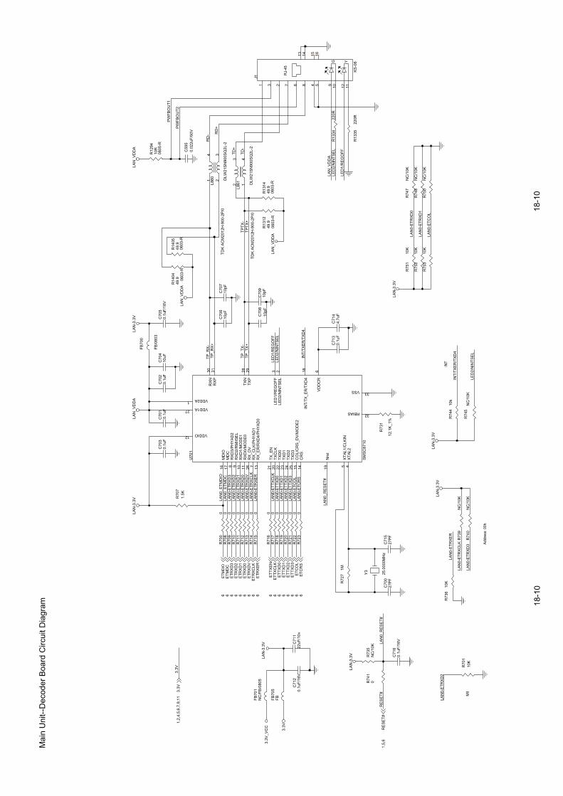
Addr
ess:
00h
MII
INT
LAN
0-E
TRX
D2
LED
2/N
INTS
EL
LAN
0_E
TMD
CLA
N0_
ETM
DIO
RE
SE
T#
TD+
INT/
TXER
/TXD
4
LAN
0-E
TRX
ER
TP_R
X-
TP_R
X+
LAN
0-E
TRX
D1
LAN
0-E
TRX
D0
LED
2/N
INTS
EL
LAN
0-ET
TXD
3
LED
1/R
EG
OFF
LAN
0-E
TRX
D2
LAN
0-E
TCR
S
LAN
0-ET
TXD
1
LAN
0-E
TCO
L
LAN
0-ET
TXD
0
LAN
0-ET
TXD
2
LAN
0-E
TRX
CLK
LAN
0-ET
TXC
LK
LAN
0-E
TRX
D3
LAN
0-E
TRX
ER
LAN
0-E
TRX
DV
LAN
0_R
ES
ET#
LAN
0_R
ES
ET#
LAN
0-E
TRX
CLK
LAN
0-E
TRX
D3
TP_T
X-
TP_T
X+
TPTX
-
3.3V
INT/
TXER
/TXD
4
LAN
_VD
DA
LED
2/N
INTS
EL
LED
1/R
EG
OFFTD
-
PW
FBO
UT1
PW
FBO
UT2
LAN
0-E
TRX
D0
LAN
0-E
TRX
D1
LAN
0-E
TCO
L
TPTX
+
RD
- RD
+
ETM
DIO
6
RE
SE
T#1,
5,6
ETC
RS
6
ETT
XD
06
ETR
XER
6ET
RXC
LK6
ETR
XD2
6
ETT
XC
LK6
ETT
XD
26
ETT
XD
16
ETR
XD3
6
ETT
XE
N6
ETR
XDV
6
ETC
OL
6E
TTX
D3
6
ETR
XD1
6
ETM
DC
6
ETR
XD0
6
3.3V
1,2,
4,5,
6,7,
9,11
LAN
-3.3
V
LAN
_VD
DA
3.3V
_VC
CLA
N-3
.3V
LAN
-3.3
V
LAN
-3.3
V
LAN
-3.3
V
LAN
-3.3
V
LAN
_VD
DA
LAN
_VD
DA
LAN
-3.3
VLA
N_V
DD
A
3.3V
C71
60.
1uF/
16V
C70
50.
1uF/
16V
R71
30
C70
10.
1uF
R13
3522
0R
C59
50.
022u
F/50
V
C70
910
pF
Y3
25.0
000M
Hz
R71
50
R71
10
R14
0449
.9 0603
-R
R73
9N
C/1
0K
FB70
1N
C/F
B/0
805
R70
00
R71
90
R70
110
K
R12
9410
R08
05-R
R14
0549
.906
03-R
C71
30.
1uF
C70
610
pF
R71
60
R71
40
R74
410
kR
736
10K
R70
80
R71
20
R75
110
K
R72
00
R72
30
R71
80
R75
210
K
RJ-
45
YG
J1
KS
-06
673 4 581 2 109 12 11
151413 16
FB70
5FB
R72
71M
R71
70
C70
710
pF
R75
310
K
C70
20.
1uF
R74
7N
C/1
0K
R70
71.
5K
R74
0N
C/1
0K
R71
00
C70
30.
1uF
L860
TDK
AC
M20
12H
-900
-2P
/0D
LW21
SN
900S
Q2L
-2
1
32
4
R13
1249
.906
03-R
C71
20.
1uF/
16V
R74
8N
C/1
0K
R74
10
U70
1
SM
SC
8710
3
515 14
32
2
1716
18
19726 13111098
30 31
21 20 22 23 24 25
28 29 6
1
27
12
4
33
LED
1/R
EG
OFF
XTA
L1/C
LKIN
CO
L/C
RS
_DV
/MO
DE
2C
RS
RBIAS
LED
2/N
INTS
EL
MD
CM
DIO
INT/
TX_E
R/T
XD
4
Nrs
t
RX
_CLK
/PH
YA
D1
RX
_DV
RX
_ER
/RX
D4/
PH
YA
D0
RX
D0/
MO
DE
0R
XD
1/M
OD
E1
RX
D2/
RM
IISE
LR
XD
3/P
HY
AD
2
RX
NR
XP
TX_E
NTX
CLK
TXD
0TX
D1
TXD
2TX
D3
TXN
TXP
VD
DC
R
VDD2A
VDD1A
VDDIO
XTA
L2
VSS
R72
10
R72
20
C71
122
uF/1
0v
R75
0N
C/1
0K
L861
TDK
AC
M20
12H
-900
-2P
/0D
LW21
SN
900S
Q2L
-2
2
41
3
R74
5N
C/1
0K
C70
810
pF
R73
1
12.1
K_1
%
R73
5N
C/1
0K
R13
1449
.906
03-R
R13
3422
0R
C70
027
PF
FB70
0
FB/0
603
R70
90
C71
44.
7uF
C71
527
PF
C70
410
uF
Mai
n U
nit--
Dec
oder
Boa
rd C
ircui
t Dia
gram
18-1
018
-10

TCK
/TR
ST
/NR
STTD
IR
TCK
TDO
TMS
GIO14GIO19GIO16GIO17GIO18GIO15
VDAC0
US
FCS
#U
SFD
OU
SFC
K
US
FDI
FE_S
FWP
#
UTX
DU
RX
D
GIO
9M
PX
1M
PX
2
XTA
L25M
O
RS
TI
RS
TI
FE_X
TALI
GA
INS
W
CD
_VR
BD
_LD
VR
DC
3O
XTA
L25M
O
CO
_B-
GIO
7
SX
VD
D
CO
_A+
CO
_B+
BD
_LD
MD
I_D
VD
FOIN
FOIP
LDD
_SE
N
RFO
-
VFV
RE
F
RFO
+
VFV
RE
F
TRIN
A
TRIN
DTR
INC
TRIN
B
V14
RE
F
VH
AV
C
TRIN
ATR
INB
LDD
_SD
IOLD
D_C
LK
TRIN
DTR
INC
RFO
+R
FO-
MD
I_D
VD
MD
I_B
D
INE
INF
ING
INH
INA
INB
INC
IND
FOIN
FOIP
GAINSWGAINSW2
LDD_SDIOLDD_CLKLDD_SEN
TLOTROFOO
FMO4
TYPWM
FMO3
FMOFMO2DMO
US
FCS
#FE
_SFC
S#
LGO1NLGO2PLGO2N
LGO1P
LGO3P
US
FDI
FE_S
FDI
LGO3NLGO4P
LGO5PLGO5N
GAINSW3
SX
VD
D
FE_SFDOFE_SFCLKFE_SFHOLD
FE_SFCS#
FE_SFWP#FE_SFDI
TRA
YIN
#TR
AY
OU
T#
MD
I_B
D
LGO
1N
LGO
3PLG
O2N
LGO
3NLG
O4P
LGO
5NLG
O5P
MU
TE2
UR
XD
UTX
D
MU
TE1
DM
SO
GIO
9
GIO
5G
IO6
FMS
O2
GIO
7
GIO
4
TXO
N
TRS
O
RX
IN
TXO
P
RX
IP
FOS
OTL
SO
FG
TRA
YP
WM
GIO12
FE_X
TALI
OMF
OS
MFD
MO
TYP
WM
FMO
2TR
O
TLO
FOO
FMO
4RSTI
FMO
3FM
SO
4FM
SO
3
AUX1
VRDCOVRDC1O
CD
_LD
VRDC2OVRDC3O
IND
INB
MPX1MPX2MPX3
INF
INA
INH
VD
AC
0
INC
ING
INE
EQBIAS
FOC
2+
SP
LLV
DD
LGO
2P
GIO
5G
IO6
CD
_HFM
DV
D_H
FM
GIO
7
GIO
4
VR
DC
OV
RD
C1O
FOC
2-
DV
D_L
D
TR-
VH
AV
C
RFO
-R
FO+
LGO
3PLG
O3N
GA
INS
W
AUX1
DV
D_H
FMC
D_V
RD
VD
_VRFO
C1+
MP
X3
VR
DC
2O
DV
D_L
D
CD
_LD
CD
_HFM
TR+
VH
AV
CG
IO6
FG
TR+
TR-
TLSO
TRA
YP
WM
V14
RE
FM
UTE
2M
UTE
1
FMS
OFM
SO
2D
MSO
FOS
OTR
SO
CO
_B-
CO
_B+
CO
_A+
FOC
1-
CO
_A-
FMS
O4
FMS
O3
TRA
YIN
#
FOC
1-FO
C1+
FOC
2-FO
C2+
CO
_A-
LGO
1P
DV
D_V
R
TXO
N
RX
IN
RX
IP
TXO
P
GIO
5
RS
TI
GA
INS
W2
FE_S
FCLK
US
FCK
FE_S
FDO
US
FDO
GIO13
SP
LLV
DD
FE_S
FHO
LD
LGO2NLGO3PLGO3NLGO4PLGO5PLGO5N
LGO1N
GA
INS
W3
TTD
IATT
RST
#A
TTD
OA
TTC
KAA
SMTT
61OI
G
TRTC
KA
AIDTT
51OI
G
AO
DTT91
OIG
A#TSRTT
41OI
G GIO
18G
IO17
TTM
SA
TTC
KATR
TCK
A
3.3V
5V_V
CC
FE_G
ND
PLA
Y#
EJE
CT#
LGO
4NLE
D1
UTX
DU
RX
D
GIO
2
GIO
8
PLA
Y#
EJE
CT#
GIO
8
LGO4N
LED
1
GIO
2
US
FDI
5
US
FCK
5
US
FCS
#5
US
FDO
5
NS
_CLK
IN_3
34
NS
_RFI
P4
NS
_RFI
N4
RS
TI5,
12
25M
_Buf
5
US
FCK
5
US
FDI
5
US
FDO
5
US
FCS
#5
VH
AV
C12
GIO
612
FG12
TR+
12TR
-12
TLSO
12TR
AY
PW
M12
V14
RE
F12
MU
TE2
12M
UTE
112
FMSO
12FM
SO
212
DM
SO12
FOS
O12
TRSO
12C
O_B
-12
CO
_B+
12C
O_A
+12
CO
_A-
12FM
SO
412
FMS
O3
12
TRA
YIN
#12
FOC
1-12
FOC
1+12
FOC
2-12
FOC
2+12
TXO
P5
RX
IN5
RX
IP5
TXO
N5
GIO
512
RS
TI5,
12
GA
INS
W2
12
3.3V
1,2,
4,5,
6,7,
9,10
TRA
YO
UT#
12
5V_V
CC
1,4,
9A
3.3V
M
A3.
3V
3.3V
FE_G
ND
FE_G
ND
FE_G
ND
FE_G
ND
FE_G
ND
FE_G
ND
5V_V
CC
FE_G
ND
AV
CC
FE_G
ND
M
FE_G
ND
FE_G
ND
VC
C_H
FMA
VC
C
FE_G
ND
FE_G
ND
VC
C_B
D_L
D
FE_G
ND
FE_G
ND
VH
AV
CV
14R
EF
VFV
RE
F
VC
C_H
FM
FE_G
ND
A1.
2V
AV
CC
VC
C_P
DIC
VC
C_L
D
VC
C_O
PU
VC
C_B
D_L
D
FE_G
ND
M3.3V
D3.
3V
SP
LLV
DD
FE_G
ND
FE_G
ND
A3.
3V
A1.
2V
A1.
2V
A3.
3V
D3.3V
A3.3V
FE_G
ND
D1.2VD3.3V
D1.
2V
M
D3.3V
V14
RE
F
A1.
2V
SX
VD
D
D1.2V
FE_G
ND
FE_G
ND
D1.2V
A1.
2V
M3.3VD1.2V
A1.
2V
A3.
3V
A1.
2V
D3.3V
FE_G
ND
FE_G
ND
VC
C_P
DIC
VC
C_L
D
A3.
3V
A3.
3V
FE_G
ND
A3.
3V
FE_G
ND
FE_G
ND
FE_G
ND
FE_G
ND
VC
C
3.3V
F_C
108
NC
F_C
110
0.1u
F
F_R
590
TP50
F_L1
010
uH
TP48
F_C
1120
.1uF
F_R
121
39
F_C
109
0.1u
F
F_C
132
330p
F
TP8
F_R
138
10K
F_C
100
2.2u
F
TP52
TP4
F_C
125
330p
F
F_C
95
2.2u
F
TP62
R81
8N
C
F_C
105
2.2u
F
F_R
147
470
F_N
C26
F_R
4720
K
F_R
700
F_R
129
NC
F_N
C13
TP46
F_C
121
0.1u
F
TP57
F_C
9810
uF
TP39
F_C
102
2.2u
F
F_Q
162S
B11
32
F_C
1260
.1uF
U10
0G
MT8
530_
DD
R2
U7
N5 J1 W5
P4
R5
N3
R7
P2
N1
R3 T6 U9
V6
U1
R1 T2 W7
V2
U3
P8 T4 U5
Y4
Y2
W1
W3
V4
AA
7W
9A
B8
AC
7
G3
E3
D2
H8
E5
L9 G5
G9
J5 J7 AP
8A
R1
AR
3A
P2
AN
1A
P6
AN
7A
L7A
M6
AH
2A
G3
V10
AG
1A
H4
AK
4A
J5A
G9
AD
8A
H8
AJ3AJ1K4AA9M4L3L1M2P6G1M6L5K2J3R9T10M10AB12U11M8H2AV2G7AW1AW3H6L7F2K6E1C1F4W11T8
AN5AA5Y6AA1AA3AC3AB4AC1AB2AC5AB6V8AD2AE7AF8AE5AD6AG5AG7AF6AM8AH6AD4AE3AE1AF4AF2Y10N7AC9AB10AE9AT10Y8
N11
N9
P10
FE_V
14FE
_VFV
RE
FFE
_HA
VC
FE_A
GN
DFE
_TR
INA
FE_T
RIN
BFE
_TR
INC
FE_T
RIN
DFE
_IN
AFE
_IN
BFE
_IN
CFE
_IN
DFE
_AV
DD
33_2
FE_I
NE
FE_I
NF
FE_I
NG
FE_I
NH
FE_A
GN
DFE
_FO
IPFE
_FO
INFE
_AV
DD
12_1
FE_F
PD
OD
VD
FE_F
PD
OC
DFE
_RFI
NFE
_RFI
PFE
_RFI
P2
FE_R
FIN
2FE
_RE
G_C
AP
FE_A
GN
DFE
_AV
DD
33_3
FE_A
VD
D12
_3FE
_AV
DD
12_4
FE_F
GFE
_GIO
2FE
_GIO
11FE
_GIO
10FE
_GIO
9FE
_GIO
8FE
_GIO
7FE
_GIO
6FE
_GIO
5FE
_GIO
4FE
_AV
DD
12_R
XFE
_SR
XP
FE_S
RX
NFE
_STX
NFE
_STX
PFE
_STX
VD
D12
FE_S
PLL
VD
D12
FE_S
VD
D33
FE_S
XV
DD
33FE
_PLA
Y#
FE_L
IMIT
FE_D
VD
D12
IFE
_GIO
3FE
_EJE
CT#
FE_T
RA
YO
UT
FE_T
RA
YIN
#FE
_GIO
1FE
_GIO
0FE
_FS
OU
RC
E
FE_XTAL25MIFE_XTAL25MO
FE_EQBIASFE_AVDD33_LVDS
FE_AUX1FE_VDAC0
FE_VWDC3OFE_VWDC2OFE_VWDC1O
FE_VRDC0FE_RSTI
FE_MPXOUT1FE_MPXOUT2FE_MPXOUT3FE_AVDD12_2
FE_DVDD12IFE_MVDDQ
FE_DVDD33OFE_DVDD12IFE_MVDDQ
FE_JTDOFE_JRTCLK
FE_JTCLKFE_JTMSFE_JTDI
FE_JTRST#FE_SFWP#
FE_SFDIFE_SFCS#FE_SFDO
FE_SFCLKFE_SFHOLD#FE_DVDD12IFE_DVDD12I
FE_SAGNDFE_LVDS_1PFE_LVDS_1NFE_LVDS_2PFE_LVDS_2NFE_LVDS_3PFE_LVDS_3NFE_LVDS_4PFE_LVDS_4NFE_LVDS_5PFE_LVDS_5NFE_AVDD33_4FE_CFREQFE_OSCENFE_CMODFE_GAINSW1FE_GAINSW2FE_GAINSW3FE_FMO3FE_FMO4FE_TLOFE_TROFE_FOOFE_TRAYPWMFE_FMOFE_FMO2FE_DMOFE_DVDD12IFE_DVDD33OFE_DVDD33OFE_DVDD33OFE_GIO12FE_GIO13FE_AGNDFE
_DV
DD
33O
FE_D
VD
D33
OFE
_DV
DD
33O
F_C
1283
30pF
F_C
1170
.1uF
F_N
C14
TP58
TP42
F_R
115
0
F_C
131
0.1u
F
TOP
XP
6
HE
AD
ER
45
SM
D0.
5 TO
P1 2 3 4 5 6 7 8 9 10 11 12 13 14 15 16 17 18 19 20 21 22 23 24 25 26 27 28 29 30 31 32 33 34 35 36 37 38 39 40 41 42 43 44 45
46 47
FCS
2+FC
S2-
TRK
+FC
S1+
TRK
-FC
S1- A-
B-
A+
B+
VC
C_C
LSFT
SIG
_P0
GN
D_C
LSFT A B C D SA
SB
SC
SD
SW
3(B
D)
RF+ RF-
SW
B2(
BD
)S
WB
1(B
D)
VR
EF_
PD
VC
C_+
5PD
GN
D_P
DS
W(D
VD
/CD
)G
ND
1LD
I_B
DLD
I_C
DLD
I_D
VD
GN
D1
TEM
PV
CC
(HFM
)M
ON
_CD
/DV
DM
ON
_BD
SE
L_D
VD
SE
L_C
DS
EL_
HFA
_DV
DS
EL_
HFA
_CD
GN
D1
NC
FE_G
ND
FE_G
ND
F_R
113
0
F_C
123
1000
pF
F_R
143
1KTP
59
F_R
117
470
F_C
140.
1uF
F_C
1291
000p
F
TP41
F_R
4810
K
XP
7
4x1
W/H
OU
SIN
G
1 2 3 4
F_R
57N
C/0
F_C
1180
.1uF
TP5
TP60
F_C
1272
200p
F
F_N
C22
F_Q
15
BT39
04
TP43
F_C
134
0.1u
F
TP61
F_R
150
NC
F_Q
122S
K30
18
1
23
F_L8
10uH
F_R
5810
K
F_C
119
0.1u
F
TP54
TP6
F_Q
172S
B11
32
F_N
C28
F_R
130
20K
F_R
134
10K
R81
9N
C
XP
5
NC
/10x
1D
IP10
/W/H
/P2.
0
1 2 3 4 5 6 7 8 9 10
TP53
F_C
1130
.1uF
F_C
133
0.1u
F
TP37
F_R
125
NC
F_R
144
470
TP30
F_R
148
470
F_R
118
1K
F_C
106
2.2u
F
F_C
93N
C
F_R
49N
C/2
0K
F_R
135
10K
F_C
122
0.1u
F
F_C
103
2.2u
F
TP38
F_N
C25
F_C
114
0.1u
F F_Q
14
BT39
04
TP47
F_N
C27
F_R
131
10K
F_R
136
10K
TP31
TP40
F_C
104
10uF
F_R
152
NC
/0
F_R
123
4.7
F_Q
112S
B11
32
4
F_R
126
0
F_R
145
33
F_C
115
0.1u
F
TP33
F_C
101
2.2u
F
R82
30
F_R
5023
.2K
/1%
F_C
20N
C/0
.1uF
TP32
F_R
124
4.7
F_C
1242
200p
F
F_R
137
10K
TP3
TP44
F_R
146
33F_
C10
7
2.2u
FF_
R14
11K
F_R
114
100K
F_R
119
470
F_C
99
2.2u
F
F_R
140
33
F_R
151
1K
TP49
F_L9
10uH
R28
410
K
F_Q
13
BT39
04
F_C
111
10uF
F_R
142
470
F_R
116
1K
F_C
17
0.1u
F
TP36
TP42
3
F_R
132
10K
F_R
122
33
TP45
F_R
120
39
TP34
TP7
F_C
120
2.2u
F
F_C
1160
.1uF
F_C
130
NC
F_Q
182S
K30
18
1
23
F_R
139
10K
F_R
128
NC
/12K
F_C
33
0.1u
F
F_C
135
NC
F_R
149
10K
R28
310
KF_
R13
320
K
R81
50
TP35
Mai
n U
nit--
Dec
oder
Boa
rd C
ircui
t Dia
gram
18-1
118
-11

(cha
nge
to +
9V)
Mot
or D
river
Sens
orle
ss
CO
LL
I MA
TO
RII
PIN
7:G
AIN
SW2
(GAI
NSW
)
PIN
12:
GIO
5 (V
DAC
0)
FFC
1. M
otor
+2.
Mot
or -
3. G
ND
4. S
W-2
5. S
W-1
B+ B-
A+
TRA
YIN
#
CO
A+
GIO
6FM
SO
3
FMS
O4
CO
A-
CO
B+
CO
B-
TRA
YP
WM
CO
MM
ON
TRS
OFO
SO
TLSO
FMS
O2
FMS
OD
MS
O
VU WB+ B-
A+ A-
TL-
TL+
FO-
FO+
TR+
TR-
LOA
D+
LOA
D-
V14
RE
F
MU
TE1
MU
TE2
FG
V14
RE
F
CO
MM
ON
A-
GA
INS
W2
CO
A-
GIO
5C
OA
+
RS
TI
CO
B-
CO
B+
CO
_A-
CO
_B+
CO
_B-
CO
_A+
FB1P
xV
FMS
O4
FMS
O3
GA
INS
W2
GIO
5
RS
TI
GA
INS
W2
TR+
TR-
FOC
1-FO
C1+
VH
AV
CG
IO6
FGFOC
2-FO
C2+
TLSO
TRA
YP
WM
V14
RE
FM
UTE
2M
UTE
1FM
SO
FMS
O2
DM
SO
FOS
OTR
SO
CO
_B-
CO
_B+
CO
_A+
CO
_A-
FMS
O4
FMS
O3
TRA
YIN
#
FOC
2+FO
+FO
C2-
FO-
FOC
1+TL
+-1
COF
-LT
WVU
+12V
FB1P
xV
3.3V
TRA
YIN
#
TRA
YO
UT#
LOA
D+
LOA
D-
GN
DTR
AY
IN#
TRA
YO
UT#
LOA
D+
LOA
D-
A+ A-
B-
B+ U V W
GIO
511
RS
TI5,
11
GA
INS
W2
11
TR+
11TR
-11
FOC
1-11
FOC
1+11
VH
AV
C11
GIO
611
FG11
FOC
2-11
FOC
2+11
TLSO
11TR
AY
PW
M11
V14
RE
F11
MU
TE2
11M
UTE
111
FMS
O11
FMS
O2
11D
MS
O11
FOS
O11
TRS
O11
CO
_B-
11C
O_B
+11
CO
_A+
11C
O_A
-11
FMS
O4
11FM
SO
311
TRA
YIN
#11
+12V
1,4,
5
3.3V
1,2,
4,5,
6,7,
9,10
,11
TRA
YO
UT#
11
M
MV
CC
VC
C
AV
CC M
MV
CC
MV
CC
A3.
3V
M
VC
C_O
PU
+12V
+12V
M12
V
M
M12
V
M
MM
12V
MM
M
M
M12
V
V14
RE
F
FE_G
ND
AV
CC
FE_G
ND
FE_G
ND
D3.
3V
M3.
3V VH
AV
CV
14R
EF
D1.
2V
FE_G
ND
AV
CC
MV
CC
MV
CC
A3.
3V
A3.
3VM
VC
C
M
MV
CC
MV
CC
M
M
M
M
M
M
M
M
M
M
MV
CC M
M
A3.
3V M
VC
C
FE_G
ND
MV
CC
F_C
82N
C
R77
00
R76
60
TP122
F_C
7910
uF
R76
80
F_C
70
0.1u
F
F_C
89
NC
F_C
80
2.2u
F
F_N
C3
F_R
9710
K
TP125
F_R
107
0
F_C
7710
uF/1
0v
F_C
92
10uF
F_R
109
0
F_U
7
NC
/LB
1848
M
1 2 3 4 567910 8
Vc
IN2
EN
AS
OF
IN1
GN
DO
UT2
OU
T3O
UT4
OU
T1
F_C
83N
C
R76
20
F_R
9810
K
TP128
F_C
62
0.1u
FF_
U5
R2A
3020
9SP
1 2 3 4 5 6 7 8 9 10 11 12 13 14 15 16 17 18 19 20 21
42 41 40 39 38 37 36 35 34 33 32 31 30 29 28 27 26 25 24 23 22
SP
INS
L1IN
SL2
INS
PLI
NV
M2
SL2
+G
ND
SL2
-S
L1+
SL1
-G
ND
U V W AC
TFLG
CO
MM
ON
TES
TS
LLIM
FG EN
1E
N2
RE
FLO
INFO
INTO
INTL
IN TL-
TL+
FO-
FO+
GN
D5V
CC
TO+
TO-
GN
DLO
-LO
+V
M3
AC
TRS
TS
TTH
SP
GS
VM
1
R76
01K
F_R
110
0
F_FB
10
F_C
87
NC
R75
41K
TP120
F_C
66
4.7u
F
R76
3N
C/1
K
F_R
9610
K
XP
3
8x1
W/H
OU
SIN
G
12345678
F_R
1111
21_1
%
F_C
72
0.1u
F
R75
9N
C/0
F_C
9710
00pF
+F_
CE
1122
0uF/
16V
F_R
103
8.2K
+F_
CE
1210
0uF/
16V
F_C
90
1uF
F_R
105
NC
F_C
86
NC
F_R
104
NC
F_C
136
0.1u
F
F_C
940.
1uF
TP123
F_C
81
2.2u
F
R14
09N
C/2
2006
03-R
F_R
101
10K
TP126
R76
433
K
F_N
C5
R77
10
F_C
760.
1uF
F_C
850.
1uF
TP129 F_C
88
NC
J4CO
N1.
0-5
1 2 3 4 5
F_U
6A
PL1
117-
AD
J
1
23
ADJ/GND
OU
TIN
F_C
710.
1uF
+F_
CE
1710
0uF/
16V
U70
3
TPC
1391
G4
1 2 3 4 5 6 7 8 9 10 11 12 13 14 15161718192021222324252630 29 28 27
LED
0La
tch_
SE
TLa
tch_
CLR
SW
R_S
EQ
1S
WR
_SE
Q2
SW
R_O
UTS
EL/
XM
UTE
STE
P_E
NA
STP
1_IN
STP
2_IN
XLE
DO
NC
SW
ON
CO
LLIE
ND
ZX
RE
SE
TA
5VA
GN
DS
TP1+
STP
1-S
TP2+
STP
2-FB
1PxV
P5V
_SW
RE
G1P
xVP
GN
D_S
WR
EG
3P3V
FB3P
3VTE
ST1
Latc
h_R
SO
UT
Latc
h_X
RS
OU
TC
SW
IC
SW
O
R75
5N
C/0
TP121
R76
90
R75
61K
/NC
F_C
73
0.1u
F
F_R
154
0
F_R
108
0
F_C
64
0.1u
F
+F_
CE
1422
0uF/
16V
F_C
754.
7uF
R77
40/
NC
F_C
67
0.1u
F
R77
24.
7K06
03-R
R77
34.
7K06
03-R
R14
100 06
03-R
F_R
102
10K
F_R
153
NC
R76
133
K
F_FB
20
+F_
CE
16
100u
F/16
V
F_C
650.
1uF
F_R
112
750_
1%
XP
4C
ON
2.0-
4
1 2 3 4
F_R
9915
K
TP124
R75
81K
F_C
69
NC
/0.1
uF
R76
70
R75
7N
C/0
F_C
74
0.1u
F
TP127
F_C
7810
uF
F_N
C2
F_C
84N
C
F_C
962.
2uF
F_N
C4
R77
5N
C/0
F_R
100
10K
F_R
106
10K
R76
50
+F_
CE
1510
0uF/
16V
F_FB
30
F_C
630.
1uF
F_N
C1
+F_
CE
13N
C/ 2
20uF
/16V
F_C
68
0.1u
F
F_C
91
1uF
TP119
Mai
n U
nit--
Dec
oder
Boa
rd C
ircui
t Dia
gram
18-1
218
-12

Mai
n U
nit--
Dec
oder
Boa
rd L
ayou
t Dia
gram
Top
Layo
ut D
iagr
am
18-1
318
-13
Bot
tom
Lay
out D
iagr
am

Mai
n U
nit--
Pow
er B
oard
Circ
uit D
iagr
am
19-1
19-1

Mai
n U
nit--
Pow
er B
oard
Lay
out D
iagr
am
Top
Layo
ut D
iagr
am
19-2
19-2
Bot
tom
Lay
out D
iagr
am

:,
:
AOBC
K
AOSD
ATA3
AOM
CLK
AOSD
ATA2
AOLR
CK
AOSD
ATA1
A_M
UTE
SCL
AOSD
ATA0
SDA
DAC
_RST
#AO
SDAT
A4
SCL
SDA
A_M
UTE
DAC
_RST
#
D-1
2VD
+12V
ZER
00
AOM
CLK
R0_
OU
T
AOBC
K
L0_O
UT
AOSD
ATA0
AOLR
CK
ZER
02
AOM
CLK
R2_
OU
T
AOBC
K
L2_O
UT
AOSD
ATA2
AOLR
CK
ZER
01
AOM
CLK
R1_
OU
T
AOBC
K
L1_O
UT
AOSD
ATA1
AOLR
CK
ZER
03
AOM
CLK
R3_
OU
T
AOBC
K
L3_O
UT
AOSD
ATA3
AOLR
CK
1789
_MU
TE
A_M
UTE
MU
TE_4
DAC
_RST
#
AOBC
K
DAC
4_L_
M
AOLR
CK
SCL
DAC
4_R
_M
AOM
CLK
DAC
4_L_
P
SDA
AOSD
ATA4
DAC
4_R
_P
1789
_MU
TE
DAC
4_R
_M
1789
_MU
TE
LOU
T4
DAC
4_R
_P
DAC
4_L_
M
DAC
4_L_
P
4TL
RO
UT4
4TR
RO
UT4
ZER
011
LOU
T1
R1_
OU
TL1
_OU
T
RO
UT1
RO
UT1
ZER
000
LOU
T0
R0_
OU
TL0
_OU
T
RO
UT0
RO
UT0
ZER
022
LOU
T2
R2_
OU
TL2
_OU
T
RO
UT2
RO
UT2
ZER
033
LOU
T3
R3_
OU
TL3
_OU
T
RO
UT3
RO
UT3
OU
T-4T
RO
UT-
4TL
ZER
000
ZER
022
ZER
011
ZER
033
1SL
1SR
0FL
0FR
2CEN
2SU
B
3SBL
3SBR
0FL
0FR
2CEN
2SU
B
1SL
1SR
3SBL
3SBR
MU
TE_5
OU
T-4T
L
MU
TE_5
5M
UTE
_44
RT4-TUORT 4
4TL
MU
TE_5
MU
TE_5
5M
UTE
_44
MU
TE_4
D-1
2V
-12V
ZER
00 A_MUTEA_MUTE
ZER
01
A_MUTE
ZER
02
A_MUTE
ZER
03
+3.3
VVD
DA
A5V
+3.3
VVD
DA
A5V
A5V
A5V
A5V
A5V
D+1
2V
A5V
PIN
4/12
PIN
4/12
+3.3
VVD
DA
A5V
A5V
A5V
A5V
A5V
A5V
A5V
A5V
A5V
A5V
A5V
-12V
-12V
A5V
R10
710
K
D18
1N41
481
2
Q11
2N39
042
13
MK
3
TP36
J1
HEA
DER
24
SMD
1.0
DO
UBL
EH
24S/
P1.0
/DB
123456789101112131415161718192021222324
+
CE4
5
CD
11X/
10U
F16V
/D5H
11
C41
33pF
/J
CB8
0.1u
F
D20
1N41
481
2
+ CE1
2C
D11
X/10
UF1
6V/D
5H11
C52
82pF
/J
TP11
CB2
0.1u
F
R30
47R
R24
11K
C17
33pF
/J
TP4
TP1
+ CE4
4C
D11
X/22
UF1
6V/D
5H11
TP30
R12
010
K
C53
390p
F/J
U9
PCM
1789
1 2 3 4 5 6 7 8 9 10 11 12131415161718192021222324
LRC
K
BCK
DIN
RST
SCKI
VDD
DG
ND
VCC
1
VCO
M
AGN
D1
VOU
TL-
VOU
TL+
VOU
TR+
VOU
TR-
AGN
D2
VCC
2
AMU
TE1
ZER
O2
ZER
O1
MO
DE
MD
/SD
A/D
EMP
MC
/SC
L/FM
TM
S/AD
R0/
RSV
ADR
5/AD
R1/
RSV
MK
4
+C
E32
CD
11X/
10U
F16V
/D5H
11
R25
11K
C51
82pF
/J
R49
3K
C39
33pF
/J
+ CE3
0C
D11
X/10
UF1
6V/D
5H11
R11
210
K
R10
82K
2
+
CE2
4
CD
11X/
10U
F16V
/D5H
11
TP37
+
CE3
5C
D11
X/10
UF1
6V/D
5H11
R85
51K
R11
100
R11
347
0
PP3
2 3 4 5
9 8 7 6
1
2 3 4 5
9 8 7 6
1
L20
FB
R65
47
R12
44.
7K
R98
1.2K
+C
E10
CD
11X/
22U
F16V
/D5H
11
+
CE1
5C
D11
X/10
UF1
6V/D
5H11
R43
8.2K
+
CE3
9
CD
11X/
10U
F16V
/D5H
11
R26
11K
C18
33pF
/J
R13
8.2K
U7
DR
V602
1 2 3 4 5 6 7891011121314
+IN
R
-INR
OU
R
SGN
D
EN PVSS
CN
CP
PVD
D
PGN
D
NC
OU
TL
-INL
+IN
L
P1
AV4-
8.4-
13D:
,;
:,
123456
C59
1uF
R50
8.2K
TP38
R44
3K
TP8
C33
1200
pF/J
L10
NC
Q8
2N39
062
1 3
R33
100
R74
33
D16
1N41
48
12
+
CE3
3C
D11
X/10
UF1
6V/D
5H11
+C
E43
CD
11X/
10U
F16V
/D5H
11
U6
DR
V602
1 2 3 4 5 6 7891011121314
+IN
R
-INR
OU
R
SGN
D
EN PVSS
CN
CP
PVD
D
PGN
D
NC
OU
TL
-INL
+IN
L
+
CE2
8
CD
11X/
10U
F16V
/D5H
11
C9
220p
F/J
R27
47R
R10
100
R38
3K
R92
47R
R12
310
K
R7
3K
R91
47R
C44
1uF
R69
47
R9
8.2K
C56
82pF
/J
R12
14.
7K
C10
1200
pF/J
R71
100
C36
220p
F/J
C61
1uF
Q3
2N39
042
13
R39
100
TP31
C35
1200
pF/J
CB3
0.1u
F
CB1
0
0.1u
F
+ CE1
4C
D11
X/10
UF1
6V/D
5H11
R10
110
R/0
.5W
R45
8.2K
L1FB
+
CE4
0
CD
11X/
10U
F16V
/D5H
11
C32
220p
F/J
R29
47R
CB1
20.
1uF
L18
FB
C13
220p
F/J
R15
3K
TP5
L11
NC
TP2
Q1
2N39
042
13
D19
1N41
481
2
TP32
R36
100
C14
1200
pF/J
R70
100
R62
47R
R10
510
K
L4FB
C58
33pF
/J
R11
60
C15
33pF
/J
+C
E27
CD
11X/
22U
F16V
/D5H
11
U11
CX1
117H
-AD
J
SOT2
23
1
342
ADJ
INO
UT2
OU
T1
R76
51K
+
CE1
6C
D11
X/10
UF1
6V/D
5H11
PCM
1754
U1
1 2 3 4 5 6 710111213141516
89
BCK
DAT
A
LRC
K
DG
ND
NC
VCC
Vout
LVC
OM
ZER
OA
TEST
DEM
P
MU
TE
FMT
SCK
Vout
RAG
ND
C57
33pF
/J
L13
FB
+C
E29
CD
11X/
10U
F16V
/D5H
11
L5FB
R89
10K
R2
100
+CE4
8
CD
11X/
220U
F16V
/D6H
12
R94
4.7R
R57
11K
P3
AV2-
8.4-
13D
AV2-
8.4-
13D
123
CB7
0.1u
F
L14
FB
R10
62K
2
PCM
1754
U5
1 2 3 4 5 6 710111213141516
89
BCK
DAT
A
LRC
K
DG
ND
NC
VCC
Vout
LVC
OM
ZER
OA
TEST
DEM
P
MU
TE
FMT
SCK
Vout
RAG
ND
TP12
C19
1uF
R86
3K
R81
3K
R47
8.2K
C16
33pF
/J
U10
DR
V602
1 2 3 4 5 6 7891011121314
+IN
R
-INR
OU
R
SGN
D
EN PVSS
CN
CP
PVD
D
PGN
D
NC
OU
TL
-INL
+IN
L
R19
100
R10
010
K
R35
100
TP33
D14
1N41
48
12
TP16
L6FB
C31
1200
pF/J
TP27
R58
11K
C20
1uF
CB1
4
0.1u
F
+ CE3
1C
D11
X/10
UF1
6V/D
5H11
CB1
30.
1uF
C23
1uF
R73
3K
C42
33pF
/J
R67
36K
C60
1uF
L2FB
R10
24.
7K
C21
1uF
R11
50
Q9
2N39
062
1 3
R80
51K
+
CE2
3
CD
11X/
10U
F16V
/D5H
11
+
CE1
7C
D11
X/10
UF1
6V/D
5H11
R97
10K
L12
FB
TP10
R56
11K
D15
1N41
48
12
R61
47R
R55
11K
R82
51K
Q5
2N39
042
13
L15
FB
+CE4
9
CD
11X/
220U
F16V
/D6H
12
C55
82pF
/J
C22
1uF
C24
1uF
Q10
2N39
042
13
C37
220p
F/J
R48
3K
+
CE3
4C
D11
X/10
UF1
6V/D
5H11
R14
3K
R11
110
K
L16
FB
R834.7R
PCM
1754
U2
1 2 3 4 5 6 710111213141516
89
BCK
DAT
A
LRC
K
DG
ND
NC
VCC
Vout
LVC
OM
ZER
OA
TEST
DEM
P
MU
TE
FMT
SCK
Vout
RAG
ND
+
CE3
6C
D11
X/10
UF1
6V/D
5H11
Q6
2N39
042
13
+
CE3
7C
D11
X/10
UF1
6V/D
5H11
+
CE5
CD
11X/
10U
F16V
/D5H
11
+C
E11
CD
11X/
10U
F16V
/D5H
11
R1
100
R4
100
TP34
TP26
D21
1N41
481
2
R10
910
K
R11
910
K
+C
E46
CD
11X/
10U
F16V
/D5H
11
Q2
2N39
042
13
R37
100
CB6
0.1u
F
L19
FB
R34
100
R96
10K
R11
447
0
+
CE2
5
CD
11X/
10U
F16V
/D5H
11C
431u
F
TP6
TP3
R16
3K
R8
8.2K
U4
DRV602
1 2 3 4 5 6 7891011121314
+IN
R
-INR
OU
R
SGN
D
EN PVSS
CN
CP
PVD
D
PGN
D
NC
OU
TL-INL
+IN
L
C45
1uF
CB5
102/
1uF
C40
33pF
/J
CB1
0.1u
F
R12
610
K
+
CE6
CD
11X/
10U
F16V
/D5H
11
+C
E13
CD
11X/
10U
F16V
/D5H
11
+
CE7
CD
11X/
10U
F16V
/D5H
11
TP18
C38
1200
pF/J
+
CE3
8C
D11
X/10
UF1
6V/D
5H11
R11
02K
2
TP35
TP23
D17
1N41
48
12
R10
310
K
L3FB
L22
FB
R11
74.
7K
R77
100
C54
390p
F/J
PP4
2 3 4 5
9 8 7 6
1
2 3 4 5
9 8 7 6
1
U12
7805
TO-2
52-3
/SM
D
2
13
GND
INO
UT1
R95
10K
CB4
0.1u
F
+CE4
7
CD
11X/
220U
F16V
/D6H
12
R11
84.
7K
C8
220p
F/J
R5
100
CB1
10.
1uF
R17
8.2K
+
CE1
8C
D11
X/10
UF1
6V/D
5H11
U3
DR
V602
1 2 3 4 5 6 7891011121314
+IN
R
-INR
OU
R
SGN
D
EN PVSS
CN
CP
PVD
D
PGN
D
NC
OU
TL
-INL
+IN
L
C7
1200
pF/J
+C
E8
CD
11X/
22U
F16V
/D5H
11
R75
3K
TP17
L21
FB
R72
100
R60
47R
+
CE9
CD
11X/
10U
F16V
/D5H
11
MK
1
PCM
1754
U8
1 2 3 4 5 6 710111213141516
89
BCK
DAT
A
LRC
K
DG
ND
NC
VCC
Vout
VCO
M
ZER
OA
TEST
DEM
P
MU
TE
FMT
SCK
Vout
RAG
ND
+C
E41
CD
11X/
22U
F16V
/D5H
11
R41
100
R10
42K
2
+ CE50
CD
11X/
220U
F16V
/D6H
12
C47
1uF
Q4
2N39
042
13
R12
510
K
P2
AV4-
8.4-
13D:
,;
:,
123456
C46
1uF
R59
47R
R46
100
+C
E26
CD
11X/
22U
F16V
/D5H
11
+
CE4
2
CD
11X/
10U
F16V
/D5H
11
R28
47R
R66
36K
R3
100
R99
2K
C12
220p
F/J
MK
2
C34
220p
F/J
R87
36K
L17
FB
R12
210
K
R88
36K
C48
1uF
CB9
0.1u
F
C11
1200
pF/J
Q7
2N39
042
13
TP29
R23
11K
TP20
Mai
n U
nit -
- Out
put B
oard
Circ
uit D
iagr
am
20-1
20-1

Mai
n U
nit -
- Out
put B
oard
Lay
out D
iagr
am
Top
Layo
ut D
iagr
am
Bot
tom
Lay
out D
iagr
am
20-2
20-2

Mai
n U
nit E
xplo
ded
View
21-1
21-1

22-1
Packing Exploded View

Repair the BD set with mainboard
issue
Order new mainboard for
repair
Check the original BD loader
If there is a N digits label
attached on the loader?
Record all N digits and then continue to exchange the
new board
Yes
If no label found, go to the text file to check production
data
No
Download the latest SW and
proceed upgrade
Follow appendix A to enter “Service Mode” for OPU
and new mainboard alignment
Finished alignment and then normal functional check,
return to consumer if no issue
Follow appendix B to get the N digits for OPU and new
mainboard alignment
Can you find the N digits?
In this case, we cannot proceed OPU and new mainboard alignment with original loader, please
exchange old loader with new one together, because only new loader will attach the N digits
label
place sticker with N digits on the
loader for future repairs
Yes
No
Note: N digits can be N=3,6,...

Appendix A – how to proceed OPU and mainboard alignment?
1. Record all the N digits on attached label of the original loader or new loader spare part (if replaced a new loader), for example:
Note: Some sets do not have this label, please follow appendix B to get the N digits from text file and program. After that, place a sticker with “N digits” on the loader for future repairs.
2. Power on the set and connect with TV, press “5” “1” “7” “7” by remote control when in the HOME menu, it will enter a special menu with 6 options. Use “Up” and “Down” button by remote control to select option “[5] Service”
3. When you see this screen, please plug a USB drive. After that press “Enter” to install barcode.
Note: We need to plug‐in USB drive otherwise you cannot proceed to next step. This is for saving data in case of failure happen, and then loader supplier could use this information to investigate.

4. Input all N digits by remote control, then press “Back” and then press “Enter” to save the setting.
5. If setting is saved successfully, it will display “Pas” on screen. Otherwise, it will display “Fail” on screen. If “fail”, confirm the N digits information again. (this is like a password, it failed if we input the wrong password)
6. Press “Stop” key on remote control to go back the HOME menu again, and then press “5” “1” “7” “7” by remote control to enter a special menu with 6 options again. Use “Up” and “Down” button by remote control to select option “[6] Laser Check”
7. If the cable is well connected and welded protection point is ok, it will display “Passe” on screen.
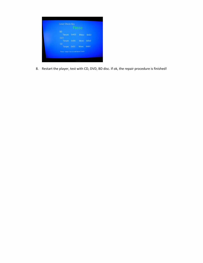
8. Restart the player, test with CD, DVD, BD disc. If ok, the repair procedure is finished!

Appendix B – how to get the 3 digits from text file?
1. Open the text file, search the original mainboard number in order to get the corresponding 2D barcode & digit. E.g. Find board number 4091100636763, then you will get “00PJBGFF08FC000801000000000000000000293022‐12.0‐01.1‐00.81D69‐4091100636763”, then the corresponding 2D barcode & digit is “00PJBGFF08FC000801000000000000000000293022‐12.0‐01.1‐00.81D69”
2. Run barcode converter software (Rpower.exe file) on your PC, just press “OK” if you see this pop up message!
3. Copy and paste “00PJBGFF08FC000801000000000000000000293022‐12.0‐01.1‐00.81D69” on Bar Code column, Press “Write” button, you will get “N digits” on your PC screen.
4. Place a sticker with “N digits” on the loader for future repairs.

Revision List
Revision ListVersion 1.0 * Initial Release
23-1
Version 1.1 * OPU setting alignment procedure added in page 24.


![Philips-Magnavox Chassis TPE1.0U-LA [SM]](https://static.fdocuments.in/doc/165x107/55cf978a550346d0339233f3/philips-magnavox-chassis-tpe10u-la-sm.jpg)
![Philips Chassis Em7u-Aa Sm [ET]](https://static.fdocuments.in/doc/165x107/552465d74a7959fa488b4740/philips-chassis-em7u-aa-sm-et.jpg)


![Philips Cdm12.1 Laser Sm [ET]](https://static.fdocuments.in/doc/165x107/5449f238b1af9f1c6b8b458f/philips-cdm121-laser-sm-et.jpg)