PEX6-COPinnovative-dsp.com/wp-content/uploads/2018/02/PEX6-COP_datasheet… · PEX6-COP DESCRIPTION...
13
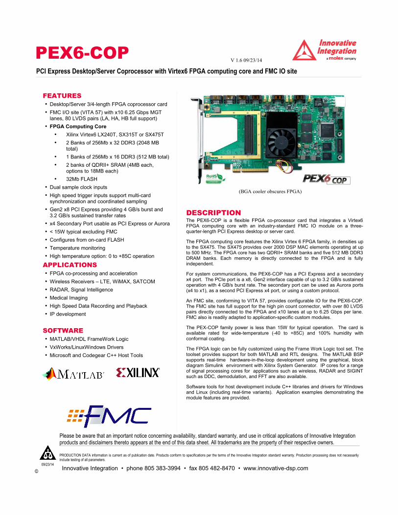
PEX6-COP DESCRIPTION The PEX6-COP is a flexible FPGA co-processor card that integrates a Virtex6 FPGA computing core with an industry-standard FMC IO module on a three- quarter-length PCI Express desktop or server card. The FPGA computing core features the Xilinx Virtex 6 FPGA family, in densities up to the SX475. The SX475 provides over 2000 DSP MAC elements operating at up to 500 MHz. The FPGA core has two QDRII+ SRAM banks and five 512 MB DDR3 DRAM banks. Each memory is directly connected to the FPGA and is fully independent. For system communications, the PEX6-COP has a PCI Express and a secondary x4 port. The PCIe port is a x8, Gen2 interface capable of up to 3.2 GB/s sustained operation with 4 GB/s burst rate. The secondary port can be used as Aurora ports (x4 to x1), as a second PCI Express x4 port, or using a custom protocol. An FMC site, conforming to VITA 57, provides configurable IO for the PEX6-COP. The FMC site has full support for the high pin count connector, with over 80 LVDS pairs directly connected to the FPGA and x10 lanes at up to 6.25 Gbps per lane. FMC also is readily adapted to application-specific custom modules. The PEX-COP family power is less than 15W for typical operation. The card is available rated for wide-temperature (-40 to +85C) and 100% humidity with conformal coating. The FPGA logic can be fully customized using the Frame Work Logic tool set. The toolset provides support for both MATLAB and RTL designs. The MATLAB BSP supports real-time hardware-in-the-loop development using the graphical, block diagram Simulink environment with Xilinx System Generator. IP cores for a range of signal processing cores for applications such as wireless, RADAR and SIGINT such as DDC, demodulation, and FFT are also available. Software tools for host development include C++ libraries and drivers for Windows and Linux (including real-time variants). Application examples demonstrating the module features are provided. FEATURES • Desktop/Server 3/4-length FPGA coprocessor card • FMC I/O site (VITA 57) with x10 6.25 Gbps MGT lanes, 80 LVDS pairs (LA, HA, HB full support) • FPGA Computing Core • Xilinx Virtex6 LX240T, SX315T or SX475T • 2 Banks of 256Mb x 32 DDR3 (2048 MB total) • 1 Banks of 256Mb x 16 DDR3 (512 MB total) • 2 banks of QDRII+ SRAM (4MB each, options to 18MB each) • 32Mb FLASH • Dual sample clock inputs • High speed trigger inputs support multi-card synchronization and coordinated sampling • Gen2 x8 PCI Express providing 4 GB/s burst and 3.2 GB/s sustained transfer rates • x4 Secondary Port usable as PCI Express or Aurora • < 15W typical excluding FMC • Configures from on-card FLASH • Temperature monitoring • High temperature option: 0 to +85C operation APPLICATIONS • FPGA co-processing and acceleration • Wireless Receivers – LTE, WiMAX, SATCOM • RADAR, Signal Intelligence • Medical Imaging • High Speed Data Recording and Playback • IP development SOFTWARE • MATLAB/VHDL FrameWork Logic • VxWorks/LinuxWindows Drivers • Microsoft and Codegear C++ Host Tools Please be aware that an important notice concerning availability, standard warranty, and use in critical applications of Innovative Integration products and disclaimers thereto appears at the end of this data sheet. All trademarks are the property of their respective owners. PRODUCTION DATA information is current as of publication date. Products conform to specifications per the terms of the Innovative Integration standard warranty. Production processing does not necessarily include testing of all parameters. © 09/23/14 (BGA cooler obscures FPGA) PCI Express Desktop/Server Coprocessor with Virtex6 FPGA computing core and FMC IO site V 1.6 09/23/14 Innovative Integration • phone 805 383-3994 • fax 805 482-8470 • www.innovative-dsp.com
Transcript of PEX6-COPinnovative-dsp.com/wp-content/uploads/2018/02/PEX6-COP_datasheet… · PEX6-COP DESCRIPTION...
PEX6-COP
DESCRIPTIONThe PEX6-COP is a flexible FPGA co-processor card that integrates a Virtex6 FPGA computing core with an industry-standard FMC IO module on a three-quarter-length PCI Express desktop or server card.
The FPGA computing core features the Xilinx Virtex 6 FPGA family, in densities up to the SX475. The SX475 provides over 2000 DSP MAC elements operating at up to 500 MHz. The FPGA core has two QDRII+ SRAM banks and five 512 MB DDR3 DRAM banks. Each memory is directly connected to the FPGA and is fully independent.
For system communications, the PEX6-COP has a PCI Express and a secondary x4 port. The PCIe port is a x8, Gen2 interface capable of up to 3.2 GB/s sustained operation with 4 GB/s burst rate. The secondary port can be used as Aurora ports (x4 to x1), as a second PCI Express x4 port, or using a custom protocol.
An FMC site, conforming to VITA 57, provides configurable IO for the PEX6-COP. The FMC site has full support for the high pin count connector, with over 80 LVDS pairs directly connected to the FPGA and x10 lanes at up to 6.25 Gbps per lane. FMC also is readily adapted to application-specific custom modules.
The PEX-COP family power is less than 15W for typical operation. The card is available rated for wide-temperature (-40 to +85C) and 100% humidity with conformal coating.
The FPGA logic can be fully customized using the Frame Work Logic tool set. The toolset provides support for both MATLAB and RTL designs. The MATLAB BSP supports real-time hardware-in-the-loop development using the graphical, block diagram Simulink environment with Xilinx System Generator. IP cores for a range of signal processing cores for applications such as wireless, RADAR and SIGINT such as DDC, demodulation, and FFT are also available.
Software tools for host development include C++ libraries and drivers for Windows and Linux (including real-time variants). Application examples demonstrating the module features are provided.
FEATURES• Desktop/Server 3/4-length FPGA coprocessor card
• FMC I/O site (VITA 57) with x10 6.25 Gbps MGTlanes, 80 LVDS pairs (LA, HA, HB full support)
• FPGA Computing Core
• Xilinx Virtex6 LX240T, SX315T or SX475T
• 2 Banks of 256Mb x 32 DDR3 (2048 MBtotal)
• 1 Banks of 256Mb x 16 DDR3 (512 MB total)
• 2 banks of QDRII+ SRAM (4MB each,options to 18MB each)
• 32Mb FLASH
• Dual sample clock inputs
• High speed trigger inputs support multi-cardsynchronization and coordinated sampling
• Gen2 x8 PCI Express providing 4 GB/s burst and3.2 GB/s sustained transfer rates
• x4 Secondary Port usable as PCI Express or Aurora
• < 15W typical excluding FMC
• Configures from on-card FLASH
• Temperature monitoring
• High temperature option: 0 to +85C operation
APPLICATIONS• FPGA co-processing and acceleration
• Wireless Receivers – LTE, WiMAX, SATCOM
• RADAR, Signal Intelligence
• Medical Imaging
• High Speed Data Recording and Playback
• IP development
SOFTWARE• MATLAB/VHDL FrameWork Logic
• VxWorks/LinuxWindows Drivers
• Microsoft and Codegear C++ Host Tools
Please be aware that an important notice concerning availability, standard warranty, and use in critical applications of Innovative Integration products and disclaimers thereto appears at the end of this data sheet. All trademarks are the property of their respective owners.
PRODUCTION DATA information is current as of publication date. Products conform to specifications per the terms of the Innovative Integration standard warranty. Production processing does not necessarilyinclude testing of all parameters.
©09/23/14
(BGA cooler obscures FPGA)
PCI Express Desktop/Server Coprocessor with Virtex6 FPGA computing core and FMC IO site
V 1.6 09/23/14
Innovative Integration • phone 805 383-3994 • fax 805 482-8470 • www.innovative-dsp.com
PEX6-COPORDERING INFORMATION
Product Part Number Description
PEX6-COP 80284-1-<ER> FPGA coprocessor for desktop/server PCI Express with FMC IO site; Xilinx LX240T FPGA -2 speed grade supporting x8 Gen2 PCI Express. 2 x 4MB SRAM, 5 x 512MB DDR3 DRAM.
<ER> is environmental rating (see following table)
80284-3-<ER> Like 80280-1 except SX315T2 FPGA
80284-6-<ER> Like 80280-1 except SX475T2 FPGA
PEX6-COP FrameWork Logic
55036 PEX6--COP FrameWork Logic board support package for RTL and MATLAB. Includes technical support for one year. Check with sales for specific FMC support.
Software 57001 Malibu software installation DVD including drivers for Windows and Linux.
2 of 13Innovative Integration • phone 805 383-3994 • fax 805 482-8470 • www.innovative-dsp.com

PEX6-COP
3 of 13
Illustration 1: Block Diagram
MGT
FMC
MemCtl
DDR3
256Mb x 32
MGTPCIe
+12VPower
Connector
PCIex8
(gen2)
FLASH32Mb
8
PEX6-COP
Power
DDR3256Mb X 32
MemCtl
QDRII+36Mb
QDRII+36Mb
MemCtl
MemCtl
FMC dataLA_P/N[33:0]HA_P/N[23:0]HB_P/N[21:0]
XilinxVirtex6SX315T/SX475LX240T
FPGA
FMC I/O SiteANSI/VITA 57.1
HPC (High Pin Cnt.)
4
DDR3256Mb x 16
MemCtl
PCI Expresshost bus
DIO12 LVDS pairs2 1.5V Diff Clock6 Single Ended+power
QSE20
4
LVDS Outputsx2
LVDS Inputsx2
PPS input
ConfigFlash1Gb
DIO
MGTPCIe,
Aurora, etc..
Timing/Triggers
EventTiming(see
detail)Timingand clock inputs
Timing outputs
Other memory sizes possible (please consult factory)
XilinxXC2C384
CoolRunner-IICPLD
Secondary Communications
(4 high speed serialtransceivers with reference
clocks, see detail)
TempSensor andFan Control
FMC control
FMC DP(0..9) + Clks
FMC power
FMC M2C and BiDir Clocks
LVDS Outputsx2
Secondary Comm.User defined PCIe,Aurora, etc...
3.3V 12VWarning: connecting both PCIE and external (for 12V), or enabling internal (for 3.3V) supply may damage supplies
PCIE optional powering jumpers (factory default population shown)
Innovative Integration • phone 805 383-3994 • fax 805 482-8470 • www.innovative-dsp.com

4 of 13
Illustration 2: External Serial Communications Ports (x4)
PEX6-COP
Innovative Integration • phone 805 383-3994 • fax 805 482-8470 • www.innovative-dsp.com

5 of 13
Illustration 3: Event Timing Detail
PEX6-COP
Innovative Integration • phone 805 383-3994 • fax 805 482-8470 • www.innovative-dsp.com
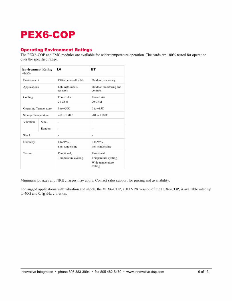
PEX6-COPOperating Environment RatingsThe PEX6-COP and FMC modules are available for wider temperature operation. The cards are 100% tested for operation over the specified range.
Environment Rating <ER>
L0 HT
Environment Office, controlled lab Outdoor, stationary
Applications Lab instruments, research
Outdoor monitoring andcontrols
Cooling Forced Air
20 CFM
Forced Air
20 CFM
Operating Temperature 0 to +50C 0 to +85C
Storage Temperature -20 to +90C -40 to +100C
Vibration Sine - -
Random - -
Shock - -
Humidity 0 to 95%,
non-condensing
0 to 95%,
non-condensing
Testing Functional,
Temperature cycling
Functional,
Temperature cycling,
Wide temperature testing
Minimum lot sizes and NRE charges may apply. Contact sales support for pricing and availability.
For rugged applications with vibration and shock, the VPX6-COP, a 3U VPX version of the PEX6-COP, is available rated upto 40G and 0.1g2/Hz vibration.
6 of 13Innovative Integration • phone 805 383-3994 • fax 805 482-8470 • www.innovative-dsp.com

PEX6-COP
Standard FeaturesFMC Site
Specification VITA 57 FMC
Type High Pin Count
High Speed Pairs
10 lanes (Tx/Rx pair)
6.25 Gbps max rate
Signal Pairs 80 pairs total
LA: 33 pairs (Vcco = 2.5V, Vref from FMC)
HA: 24 pairs (Vcco = 2.5V, Vref from FMC)
HB: 22 pairs (Vcco and Vref from FMC)
IO Standards LA, HA : LVCMOS25, LVDS25, LVDCI2, SSTL25, HSTL25
HB: all IO standards supported
Power 3.3V @ 3A (supplied by bus or on-card supply)
12V @ 1A (supplied by bus)
3.3V AUX @ 0.5A (supplied by bus)
Vadj = 2.5V @ 4A (programmable)
FPGA
Device Xilinx Virtex6
Speed Grades -2, (-1 special order)
-2 required for PCI Express x8 Gen2
Sizes SX315T = ~ 31M gates equivalent
SX475T = ~ 47.5M gates equivalent
LX240T = ~ 24M gates equivalent
Flip-Flops /Slices
SX315T: 393K /49K
SX475T: 595K / 74K
LX240T: 301K / 37K
DSP48E1 elements/ BlockRAMs
SX315T: 1344 / 704
SX475T: 2016 /1064
LX240T: 768 /416
GTP Ports x8 lanes @ 6.25 Gbps (-3 speed) to PCIe
x10 lanes @ 6.25 Gbps to FMC
x4 lanes @ 3.2 Gbps to secondary COM ports
Configuration JTAG or FLASH
In-system reprogrammable
Memories
DDR3 DRAM DDR3: 256Mx16
512MB total/device
Five devices available
400 MHz clock rate
3.2 GB/S burst transfers (400 MHz clock)
QDRII+ SRAM
8MB standard; 2 banks of 2Mx18
Options up to 16Mx18 per bank
333 MHz clock rate (standard device speed is rated for 400MHz, options up to 500 MHz)
4 GB/s sustained transfer rate (simultaneous read/writes using 500 MHz clock)
Program FLASH
Serial FLASH
32Mb
SPI interface
Configuration FLASH
Parallel FLASH
1GB
configures FPGA through CPLD loader
7 of 13Innovative Integration • phone 805 383-3994 • fax 805 482-8470 • www.innovative-dsp.com

Host Interfaces
PCI Express x8 Lanes Gen2 (requires -2 or -3 speed FPGA)
x4 Gen2 or x8 Gen2 (-1 speed FPGA)
x8 Gen2 supports 3.2GB/s sustained rates/4 GB/s burst rates
Secondary Ports x4 lanes capable of 3.2 Gbps per lane
Configurable as Aurora (4 x1 to 1 x4, PCI Express x4 , or custom protocols
4 SATA connectors for card-to-card connections
Sample Clocks and Triggering
Clock Sources 2 SMA for FMC clocks
1 SMA for clock to FPGA
Trigger Sources 2 LVDS outputs (SATA-style connector)
2 LVDS inputs (SATA-style connector)
Timing Synchronization
2 multi-drop LVDS pairs
2 open-collector flags
IDC10 connector, 2mm
Monitoring
Alerts Temperature Warning, Temperature Failure, Power Faults
Alert Timestamping
5 ns resolution, 32-bit counter
Application IO (P2)
DIO Bits 32, arranged as 16 pairs
Signal Standards LVCMOS (2.5V) – NOT 3.3 compatible
LVDS25
Power
Consumption 15W typical
Temperature Monitor Software with programmable alarms
Over-temp Monitor Disables power supplies
Power Control LPDDR3 deep sleep mode
QDR shutdown
FMC power controls
Heat Sinking Heat sink on FPGA
Optional fan for FMC cooling
Physicals
Form Factor ½ length PCI Express card
Size 8.2 x 3.8in (209 x 96 mm)
Weight 250 g (excludes FMC)
Hazardous Materials Lead-free and RoHS compliant
8 of 13
PEX6-COP
Innovative Integration • phone 805 383-3994 • fax 805 482-8470 • www.innovative-dsp.com

suited for FPGA co-processing and front-end signalprocessing applications in wireless, RADAR andmedical imaging.
FMC Module
The FMC module is a VITA57-compliant site forIO or system expansion. The FMC directlyconnects to the FPGA with 80 pairs of LVDS (160single-ended) and 10 lanes of high speed serial.The serial lanes connect to the FPGA GTP ports.
FMC modules are integrated with the PEX6-COPby including application logic in the FPGA thatprovides interface control and datacommunications. The flexible nature of the FMCinterface is also useful for custom application-specific where the pin use and interface are defined by the application logic.
Clocks and Triggers
Support for FMC integration with system devices includes clock and trigger sharing features so that multiple cards canperform simultaneous or coordinated sampling. Simple inter-card connections supports trigger sharing through two LVDSinput and two LVDS outputs. These trigger signals are provided on SATA-style connectors and support speeds up to 1 GHz.
Integration with a system timing card such as X3-Timing allows the cards to use common sample clocks and triggers,coordinated with GPS or another system reference.
FPGA Core
The PEX6-COP family has a Virtex6 FPGA and memory at its core for DSP and control. The Virtex6 FPGA is capable ofover 1 Tera MACs (SX315T operating at 500 MHz internally) with over 1300 DSP elements in the SX315T FPGA. Inaddition to the raw processing power, the FPGA fabric integrates logic, memory and connectivity features that make thePEX6-COP capable performing very demanding real-time signal processing.
The FPGA has direct access to five banks of 512 MB of DDR3 DRAM and two banks of QDRII+ SRAM. These memoriesallow the FPGA working space for computation, required by DSP functions like FFTs, and bulk data storage needed forsystem data buffering and algorithms like large FFTsy. A multiple-queue controller component in the FPGA implementsmultiple data buffers in the DRAM that is used for system data buffering and algorithm support. The SRAMs provide fastaccess for algorithm. The DDR3 is compatible with embedded processors (uBlaze).
The PEX6-COP uses the Virtex6 FPGA as a system-on-chip to integrate all the features for highest performance. As such, allIO, memory and host interfaces connect directly to the FPGA – providing direct connection to the data and control formaximum flexibility and performance. Firmware for the FPGA completely defines the data flow, signal processing, controlsand host interfaces, allowing complete customization of the functionality. Logic utilization is typically <10% of the device.
9 of 13
PCI Express
PCI Express
Host
Packetizer
PEX6-COPArchitecture and Features
The PEX6-COP architecture integrates a Xilinx Virtex6 FPGA computing core with an FMC module on a PCI Express desktop/server three-quarter-length card. System communications include a x8 Gen2 PCI Express port and a x4 secondary communications port. This architecture tightlycouples the FPGA to the FMC and enables the Data flows between the IO and the
module to perform real-time signal processing with host using a packet system
low latency and extremely high rates. It is well-
Example PEX6-COP Architecture
Data Buffer
1GBFMC Router
PEX orAurora
Port
Aurora Port
Timestamp
Connector
Connector
Innovative Integration • phone 805 383-3994 • fax 805 482-8470 • www.innovative-dsp.com

PEX6-COPCommunications Interfaces
The PEX6-COP host interface features high performance PCI Express and Aurora ports. These ports allow the PEX6-COP to be used in many system topologies, including privatedata channels between cards.
The PCIe and Aurora ports are integrated with theVelocia packet system, a powerful data network thatefficiently handles data transfers between multiple,independent data sources on the PEX6-COP and thehost processor or other cards. Data is packetized, usingpacket sizes from 32 bytes to 128KB per packet,stamped with a packet ID and destination, and are theneasily routed to other devices in the system. TheVelocia packet system is completely defined by thelogic firmware, giving complete flexibility to createany packet routing necessary to meet system latencyand transfer rate requirements.
A set of logic components for packets is provided inthe FrameWork Logic including packetizer,depacketizer, router and buffer memory controls.Packetizing includes timestamping per VITA 49. Datawithin the packets may be any format.
Secondary Ports and Digital IO
The PEX6-COP family has high speed serial data links for multi-card system interconnects. These data ports, using protocolssuch as Aurora, provide low-latency direct or switched fabric connections to the system fabric. The ports enable the PEX6-COP to integrate with other PEX6 cards or peripherals to create powerful computing and signal processing architectures.Maximum data rates, with deterministic performance can be implemented in performance-driven systems using little or noprotocol.
The secondary data port consists of x4 lanes that may be used a 4 x1 ports, or other configurations such as 2 x2, or 1 x4. Forease of use and purchasing, SATA300 cables and connectors are used on the card supporting up to 3.2Gbps data rates fullduplex on each lane.
The digital IO has 32 digital lines, routed as matched differential pairs, connected to the FPGA. An MDR68 connector on thecard rear pins out these DIO connections. Supported IO standards include LVCMOS25 and LVDS25.
Card Management Features
The PEX6-COP has power and health monitoring to protect the system from card failure. Independent monitoring of theFPGA die temperature can shut down the card to prevent damage from overheating. The card also has over-current protectionthat disconnects system power in case of failure. The FPGA also has watchdog timer functionality that may be used toprevent runaway operation.
FPGA Configuration
The modules uses a FLASH memory for the Virtex 6 FPGA image. This FLASH can be programmed in-system using asoftware applet. There are two images in the FLASH: an application image and a “golden” image as a backup.
During development, the JTAG interface to the FPGA is used for development tools such as ChipScope and MATLAB. This
10 of 13
HostPCI
ExpressRoot
Router
PEX6
PCIeAuroraOr PCIe
DevPDN=0
DevPDN=1
DevPDN=0
Router
PEX6
PCIe
DevPDN=0
DevPDN=1
DevPDN=0
AuroraOr PCIe
Real-time system architectures are enabled using Velocia packet system in VPX systems
Example System Topology:PCIe bus with private Aurora channel
Innovative Integration • phone 805 383-3994 • fax 805 482-8470 • www.innovative-dsp.com
PEX6-COPallows the FPGA image to be downloaded over the cable for debugging and test. The FPGA JTAG connector is compatible with Xilinx Platform USB Cable.
Software ToolsSoftware development tools for the module provides comprehensive support including device drivers, data buffering, card controls, and utilities that allow developers to be productive from the start. At the most fundamental level, the software tools deliver data buffers to your application without the burden of low-level real-time control of the cards. Software classes provide C++ developers a powerful, high-level interface to the card that makes real-time, high speed data acquisition easier to integrate into applications.
Software for data logging and analysis are provided with every module. Data can be logged to system memory at full rate or to disk drives at rates supported by the drive and controller. Triggering and sample rate controls allow you to use the module's performance in your applications without ever writing code. Innovative software applets include Binview which provides data viewing, analysis and import to MATLAB for large data files.
Support for the Microsoft, Embarcadero and GNU C++ toolchains is provided. Supported OSes include Windows and Linux. For more information, the software tools User Guide and on-line help may be downloaded.
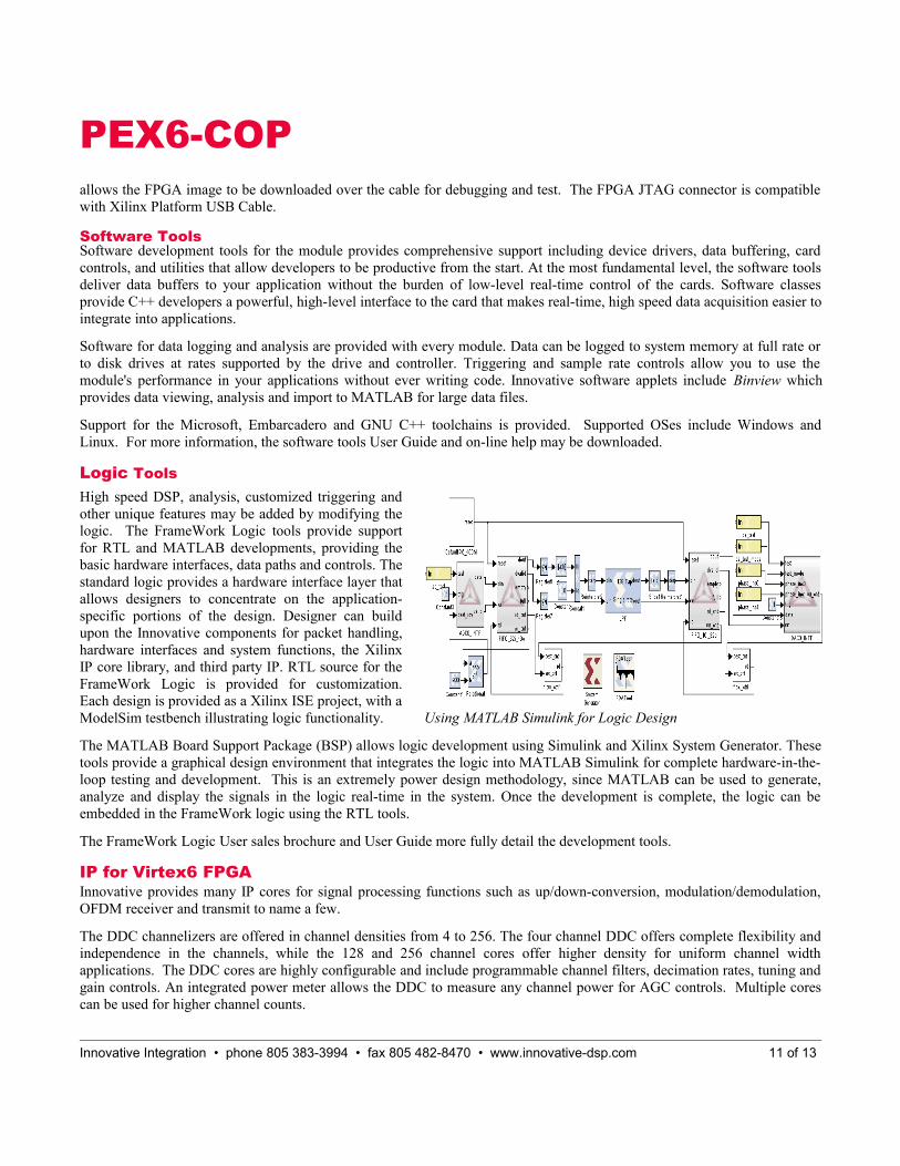
Logic ToolsHigh speed DSP, analysis, customized triggering andother unique features may be added by modifying thelogic. The FrameWork Logic tools provide supportfor RTL and MATLAB developments, providing thebasic hardware interfaces, data paths and controls. Thestandard logic provides a hardware interface layer thatallows designers to concentrate on the application-specific portions of the design. Designer can buildupon the Innovative components for packet handling,hardware interfaces and system functions, the XilinxIP core library, and third party IP. RTL source for theFrameWork Logic is provided for customization.Each design is provided as a Xilinx ISE project, with aModelSim testbench illustrating logic functionality.
The MATLAB Board Support Package (BSP) allows logic development using Simulink and Xilinx System Generator. These tools provide a graphical design environment that integrates the logic into MATLAB Simulink for complete hardware-in-the-loop testing and development. This is an extremely power design methodology, since MATLAB can be used to generate, analyze and display the signals in the logic real-time in the system. Once the development is complete, the logic can be embedded in the FrameWork logic using the RTL tools.
The FrameWork Logic User sales brochure and User Guide more fully detail the development tools.
IP for Virtex6 FPGAInnovative provides many IP cores for signal processing functions such as up/down-conversion, modulation/demodulation, OFDM receiver and transmit to name a few.
The DDC channelizers are offered in channel densities from 4 to 256. The four channel DDC offers complete flexibility and independence in the channels, while the 128 and 256 channel cores offer higher density for uniform channel width applications. The DDC cores are highly configurable and include programmable channel filters, decimation rates, tuning and gain controls. An integrated power meter allows the DDC to measure any channel power for AGC controls. Multiple cores can be used for higher channel counts.
11 of 13
Using MATLAB Simulink for Logic Design
Innovative Integration • phone 805 383-3994 • fax 805 482-8470 • www.innovative-dsp.com

PEX6-COPEach IP core is provided with a MATLAB simulation model that shows bit-true, cycle-true functionality. Signal processing designers can then use this model for channel design and performance studies. Filter coefficients and other parameters from the MATLAB simulation can be directly loaded to the hardware for verification.
Part Number
IP Core Channels Tuning Decimation Max
Bandwidth
Channel Filter
58014 IP-MDDC4 4 Fs/2^32 16 to 32768 Fs/16 Programmable 100 tap filter
58015 IP-MDDC128 128 Fs/2^32 512 to 16384 Fs/512 Programmable 100 tap filter
58528 IP-DDC256 256 Fs/2^32 512 to 16384 Fs/512 Programmable 100 tap filter
Signal processing cores for communications applications are available for Virtex6.
Part Number IP Core Features
58001 PSK Demodulation N=2,4,8,PI/4. Integrated carrier tracking and bit decision. Data rate to 160 Mbps.
58018 PSK Modulator N=2,4,8,PI/4. Data rates up to 160 Mbps.
58002 FSK Demodulation Coherent demodulation with carrier recovery,
58019 FSK Modulator FSK modulation/
58020 QAM Modulator Quadrature Amplitude Modulator.
58003 TinyDDS Tiny DDS, 1/3 to ½ size of Xilinx DDS with equal SFDR, clock rates to 400 MHz with flow control
58011 XLFFT IP core for 64K to 1M FFTs with windowing functions.
58012 Windowing IP core for Hann, Blackman and uniform data windowing functions.
58013 CORDIC IP core for sine/cosine generation using CORDIC method, resulting in 1/3 logic size of standard DDS cores.
58030 MDUC128 128-channel digital upconverter.
58036 DUC Up-conversion with interplation rates from 2-32K, programmable filters and tuning
OFDM and LTE Cores
58029 OFDM Transmitter OFDM transmit with IFFT, Windowing, Filtering, Cyclic Prefix and Upsample.
58031 OFDM Receiver OFDM receiver with synchronization, downconversion and channel filtering.
58032 LTE Dowlink Transmitter LTE downlink transmitter core for FDD mode.
58033 LTE Uplink Receiver LTE uplink receiver core for FDD mode includes 2K FFT, timing and frame synchronization using ML estimation method, decoding of SSS and PSS signals for cell ID and frame sync.
12 of 13Innovative Integration • phone 805 383-3994 • fax 805 482-8470 • www.innovative-dsp.com

IMPORTANT NOTICESInnovative Integration Incorporated reserves the right to make corrections, modifications, enhancements, improvements, and other changes to its products and services at any time and to discontinue any product or service without notice. Customers should obtain the latest relevant information before placing orders and should verify that such information is current and complete. All products are sold subject to Innovative Integration’s terms and conditions of sale supplied at the time of order acknowledgment.
Innovative Integration warrants performance of its hardware products to the specifications applicable at the time of sale in accordance with Innovative Integration’s standard warranty. Testing and other quality control techniques are used to the extent Innovative Integration deems necessary to support this warranty. Except where mandated by government requirements, testing of all parameters of each product is not necessarily performed.
Innovative Integration assumes no liability for applications assistance or customer product design. Customers are responsible for their products and applications using Innovative Integration products. To minimize the risks associated with customer products and applications, customers should provide adequate design and operating safeguards.
Innovative Integration does not warrant or represent that any license, either express or implied, is granted under any Innovative Integration patent right, copyright, mask work right, or other Innovative Integration intellectual property right relating to any combination, machine, or process in which Innovative Integration products or services are used. Information published by Innovative Integration regarding third-party products or services does not constitute a license from Innovative Integration to use such products or services or a warranty or endorsement thereof. Use of such information may require a license from a third party under the patents or other intellectual property of the third party, or a license from Innovative Integration under the patents or other intellectual property of Innovative Integration.
Reproduction of information in Innovative Integration data sheets is permissible only if reproduction is without alteration and is accompanied by all associated warranties, conditions, limitations, and notices. Reproduction of this information with alteration is an unfair and deceptive business practice.
Innovative Integration is not responsible or liable for such altered documentation. Resale of Innovative Integration products or services with statements different from or beyond the parameters stated by Innovative Integration for that product or service voids all express and any implied warranties for the associated Innovative Integration product or service and is an unfair and deceptive business practice. Innovative Integration is not responsible or liable for any such statements.
For further information on Innovative Integration products and support see our web site:
www.innovative-dsp.com
Mailing Address: Innovative Integration
741 Flynn Rd., Camarillo, California 93012
Copyright ©2018, Innovative Integration
Innovative Integration • phone 805 383-3994 • fax 805 482-8470 • www.innovative-dsp.com 13 of 13
PEX6-COP