Performance and Reliability Characteristics of … (2).… · Performance and Reliability...
8
Performance and Reliability Characteristics of 1200 V, 100 A, 200 o C Half-Bridge SiC MOSFET-JBS Diode Power Modules James D. Scofield and J. Neil Merrett Air Force Research Laboratory 1950 Fifth St WPAFB, OH 45433 937-255-5949 James Richmond and Anant Agarwal CREE, Inc. 4600 Silicon Dr Durham, NC 27703 Scott Leslie Powerex, Inc. 173 Pavilion Lane Youngwood, PA 15697 [email protected] Abstract A custom multi-chip power module packaging was designed to exploit the electrical and thermal performance potential of silicon carbide MOSFETs and JBS diodes. The dual thermo-mechanical package design was based on an aggressive 200 o C ambient environmental requirement and 1200 V blocking and 100 A conduction ratings. A novel baseplate-free module design minimizes thermal impedance and the associated device junction temperature rise. In addition, the design incorporates a free-floating substrate configuration to minimize thermal expansion coefficient induced stresses between the substrate and case. Details of the module design and materials selection process will be discussed in addition to highlighting deficiencies in current packaging materials technologies when attempting to achieve high thermal cycle life reliability over an extended temperature range. Keywords: High temperature, SiC power module, SiC MOSFET, reliability testing. Introduction Increasing emphases on electrical power functionality and energy conservation is driving an increased demand for reliable, efficient, power conversion, drive, and distribution technologies for automotive, aircraft, and consumer product applications. In addition, an increasing number of these power subsystem components would benefit significantly from an extended temperature range capability [1]. The potential volume, weight, design flexibility, and cost advantages of relaxing thermal design constraints is significant. A 150-200 o C rated power technology could enable elimination of the cost and complexity of dedicated power electronics coolant loops in hybrid and electric vehicles, as well as facilitate critical weight reductions in more-electric aircraft actuator drive and power conditioning equipment subsystems [2,3,4]. As a leading candidate to provide the performance required for these applications, silicon carbide (SiC) device technology is approaching the maturity level necessary for practical deployment consideration. In this paper we report on the performance and initial reliability characteristics of recently developed second generation (Gen II) 1200V, 100A, SiC MOSFET/JBS-diode dual-switch power modules. SiC module electrical characteristics were evaluated at temperatures up to 250°C, and performance comparisons to equivalently rated IGBT modules were accomplished over the temperature range of 25- 150°C. The 200 o C temperature rating objective of the SiC modules necessitated an intentional consideration of all aspects of the package design. Although the operational capability of SiC die at these temperatures is well established, reliable functionality is ultimately dependent upon the utilization of appropriate metallurgies, dielectric encapsulants, interconnection schemes, substrate layout, and the minimization of thermal expansion coefficient (CTE) mismatch stresses. High temperature reverse bias (HTRB), power cycling, and ambient (-40 to 250°C) temperature cycling reliability test results highlight the relative success and of these design considerations, and more International Conference on High Temperature Electronics International Microelectronics & Packaging Society May 2010 Albuquerque, NM
-
Upload
truongmien -
Category
Documents
-
view
227 -
download
0
Transcript of Performance and Reliability Characteristics of … (2).… · Performance and Reliability...
Performance and Reliability Characteristics of 1200 V, 100 A, 200oC Half-Bridge SiC MOSFET-JBS Diode Power Modules
James D. Scofield and J. Neil Merrett
Air Force Research Laboratory 1950 Fifth St
WPAFB, OH 45433 937-255-5949
James Richmond and Anant Agarwal
CREE, Inc. 4600 Silicon Dr
Durham, NC 27703
Scott Leslie Powerex, Inc.
173 Pavilion Lane Youngwood, PA 15697
Abstract
A custom multi-chip power module packaging was designed to exploit the electrical and thermal performance potential of silicon carbide MOSFETs and JBS diodes. The dual thermo-mechanical package design was based on an aggressive 200oC ambient environmental requirement and 1200 V blocking and 100 A conduction ratings. A novel baseplate-free module design minimizes thermal impedance and the associated device junction temperature rise. In addition, the design incorporates a free-floating substrate configuration to minimize thermal expansion coefficient induced stresses between the substrate and case. Details of the module design and materials selection process will be discussed in addition to highlighting deficiencies in current packaging materials technologies when attempting to achieve high thermal cycle life reliability over an extended temperature range.
Keywords: High temperature, SiC power module, SiC MOSFET, reliability testing.
Introduction
Increasing emphases on electrical power functionality and energy conservation is driving an increased demand for reliable, efficient, power conversion, drive, and distribution technologies for automotive, aircraft, and consumer product applications. In addition, an increasing number of these power subsystem components would benefit significantly from an extended temperature range capability [1]. The potential volume, weight, design flexibility, and cost advantages of relaxing thermal design constraints is significant. A 150-200oC rated power technology could enable elimination of the cost and complexity of dedicated power electronics coolant loops in hybrid and electric vehicles, as well as facilitate critical weight reductions in more-electric aircraft actuator drive and power conditioning equipment subsystems [2,3,4]. As a leading candidate to provide the performance required for these applications, silicon carbide (SiC) device technology is approaching the maturity level necessary for practical deployment consideration. In this paper we
report on the performance and initial reliability characteristics of recently developed second generation (Gen II) 1200V, 100A, SiC MOSFET/JBS-diode dual-switch power modules. SiC module electrical characteristics were evaluated at temperatures up to 250°C, and performance comparisons to equivalently rated IGBT modules were accomplished over the temperature range of 25-150°C. The 200oC temperature rating objective of the SiC modules necessitated an intentional consideration of all aspects of the package design. Although the operational capability of SiC die at these temperatures is well established, reliable functionality is ultimately dependent upon the utilization of appropriate metallurgies, dielectric encapsulants, interconnection schemes, substrate layout, and the minimization of thermal expansion coefficient (CTE) mismatch stresses. High temperature reverse bias (HTRB), power cycling, and ambient (-40 to 250°C) temperature cycling reliability test results highlight the relative success and of these design considerations, and more
International Conference on High Temperature Electronics International Microelectronics & Packaging Society May 2010 Albuquerque, NM

importantly, illustrate material development needs for wide temperature range power applications.
Module Design
Gen I modules utilized a modified commercial IGBT form factor with polyphenyl sulfide (PPS) case material and 170 W/mK AlN substrates, 221oC eutectic 96.5Sn 3.5Ag solder, and low CTE (~4 ppm/K) Cu-C baseplate components to satisfy intermediate 150oC heatsink temperature (TSink) Details of the Gen I module design are described in [5].
More extensive material analysis and design variations were carried out in order to reach the Gen II temperature goals of 200°C. Figure 1 shows a photograph of a Gen II module with the lid removed.
Figure 1. (Above) Photograph of a Gen 2 module design with lid removed and no encapsulation. (Below) Schematic diagram of the module.
Figure 2. Cross-section of Gen II module design.
Figure 2 shows a cross-section of the Gen II design. A notable change in this design from the Gen I cinfiguration is the absence of a baseplate. Here, the cooling fins are soldered with 95Pb5Sn solder directly to the direct bonded copper of the ceramic substrate. This reduces the thermal resistance from chip to air and eliminates the mechanical stress due to substrate-to-baseplate CTE mismatch. The case material used was the machinable polyimide Torlon®, which has a maximum temperature rating of 260°C. Aluminum nitride was chosen as a substrate material because of its high thermal conductivity and its close CTE match to the SiC die (AlN 4.5, SiC 3.8 ppm/K).
Electrical Performance Characterization
Fabricated Gen II SiC MOSFET phase-leg modules were characterized for static DC electrical performance metrics. On-state conduction loss measurements were made, at junction temperatures up to 250oC, for drain current (ID) values of 10 to 120 A per dual switch (two 56mm2 MOSFETs). Representative average switch forward voltage (VDS) as a function of ID is shown in Figure 3, with
Figure 3. VDS(ID) of the SiC MOSFET modules showing temperature dependence to 250oC. Si IGBT data at 25 and 150oC shown for comparison.
0.0
0.5
1.0
1.5
2.0
2.5
3.0
0 20 40 60 80 100 120
Vds,
Vce
sat (
V)
Ids, Ice (A)
1200V SiC MOSFET vs Si IGBTConduction Loss Comparison
SiC Gen II 25CSi IGBT 25CSiC Gen II 150CSi IGBT 150CSiC Gen II 200CSiC Gen II 250C
International Conference on High Temperature Electronics International Microelectronics & Packaging Society May 2010 Albuquerque, NM

temperature parameterizing the family of curves. Also included in the data of Figure 3 are the 25°C and 150°C VCE data taken from equivalently rated 1200 V, 100 A Si IGBT dual modules (CM100DY-24NF) for comparison. The data reflects a significant MOSFET advantage in on-state 100 A conduction losses with VDS values 0.79 and 0.92 V lower than corresponding VCE values for the Si IGBT at 25 and 150°C, respectively. At 200°C the SiC module losses increase approximately 19% above their 150°C value at ID=100 A, but are still lower than the IGBT losses would be at 100 A and 25°C. Forward blocking leakage characteristics (IDSS) for the SiC modules are well represented by the data shown in Figure 4, in which curves for data collected over the 25-250°C
Figure 4. Drain-source forward blocking leakage current data for 25-250°C junction temperatures. Data shown for VGS=-10V.
temperature range are plotted. The leakage characteristic data shown are for gate biases of VGS= -10V. Module switch leakage data for VGS=0V, over this same temperature range, were found to be nominally 2X–4X higher, due primarily to the threshold voltage temperature dependence, as shown in Figure 5. Threshold voltage for the SiC parallel MOSFET switches is defined as the gate bias required to induce 10 mA of drain current with 10 V across the device. Although SiC MOSFET leakage characteristics are several orders of magnitude lower than Si IGBT values at 150°C, and comparable at 25°C, negative gate biases were utilized in HTRB accelerated stress reliability testing to minimize nuisance trip-offs and increase module test hours. In addition, reliable dynamic performance in high dI/dt applications will likely necessitate the use of negative off-state gate biases until fabrication process advances yield improved MOSFET threshold characteristics. Dynamic measurements and characterization of the SiC MOSFET modules
parasitic impedances are currently ongoing and will be reported in a subsequent publication.
Figure 5. Typical SiC MOSFET gate threshold voltage characteristics as a function of temperature.
High Temperature Reverse Bias Testing
To test for stability over time, a complete module was potted with Wacker RT 745S gel and was held at a VDS of 600 V and VGS of -5 V at 200, 225, and finally 250°C for hundreds of hours while monitoring IDS current. Leakage current data is shown in Figure 6
Figure 6. High temperature reverse bias test data for a complete potted module without cooling fins.
Leakage current increased as expected with increasing temperature and remained relatively stable at 250°C for over 700 hrs. After this time the test setup experienced a series of trips that interrupted the reverse biasing. The temperature, however, was maintained at 250°C. During this time the reverse leakage current increased from around 250 µA to above 600 µA and then decreased and stabilized at around 350 µA. After a total test time of around 1500 hours the test was stopped and the module was inspected. Upon removal of the lid the RT-745S encapsulant was found to have hardened and cracked as seen in Figure 7. The extensive cracking of the encapsulant is believed to have occurred during final cool-down of the module. Even though the encapsulant will handle 250°C for short periods of
0
20
40
60
80
100
120
140
160
100 300 500 700 900 1100
Idss
(uA)
Vdss (V)
SiC Gen II MOSFET Idss(T) , Vgs=-10V
25C
100C
150C
200C
250C
0.00
0.50
1.00
1.50
2.00
2.50
0 50 100 150 200 250
Gat
e Th
resh
old
Volta
ge (V
)
Junction Temperature (C)
1.2kV, 100A SiC MOSFET: Vgth(T)
International Conference on High Temperature Electronics International Microelectronics & Packaging Society May 2010 Albuquerque, NM

time, it is clearly unsuitable for extended periods at that temperature.
Figure 7. Module after 1500 hrs HTRB testing showing cracked RT-745S encapsulant.
Several materials are currently being evaluated in a search for a suitable high temperature encapsulant material. Thermal Cycling
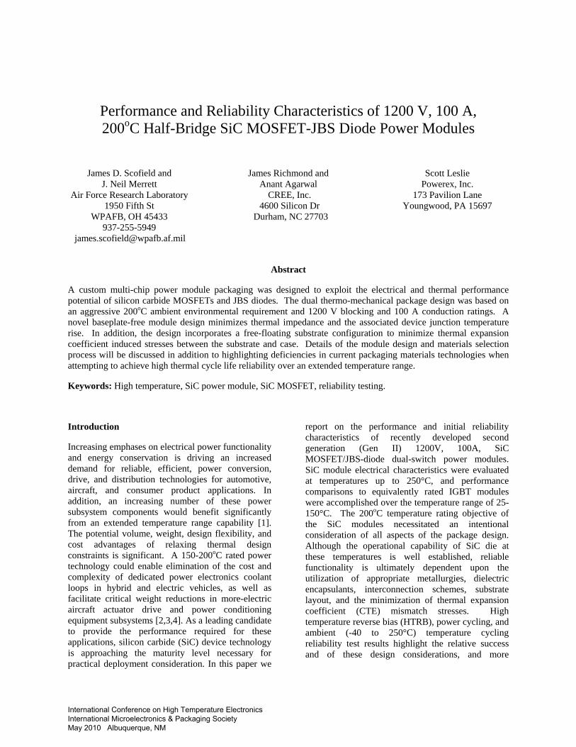
Chips were soldered to DBC AlN substrates with 95Pb5Sn solder. The chip/substrate assemblies were then cycled from -55°C to +200°C by shuttling between dual chambers. Figure 8 shows a substrate assembly with mechanical die after only 100 cycles. The red circled areas indicate regions where the DBC metallization has peeled from the substrate and where the S1D2 strap solder joint has failed.
Table 1 shows a list of encapsulant materials currently being considered. Of those listed, the ceramic filled adhesives, Resbond™ 919 and 920 [6], as well as the silicone casting compound, Duraseal™ 1533 [6], are the only materials that have held up during the -55 to 200°C, air to air shock cycling and the high temperature reverse bias testing. In addition to those materials listed in Thermal Cycling
Chips were soldered to DBC AlN substrates with 95Pb5Sn solder. The chip/substrate assemblies were then cycled from -55°C to +200°C by shuttling between dual chambers. Figure 8 shows a substrate assembly with mechanical die after only 100 cycles. The red circled areas indicate regions where the DBC metallization has peeled from the substrate and where the S1D2 strap solder joint has failed.
Table 1, two versions of polyimide foam, PerForma-H™ from GFT Corp. [7], are being evaluated. Packaged JBS diodes have been potted with the two
foams and have undergone HTRB testing at 250°C and 600 V. The samples remain stable after for more than 300 hours under these conditions. Additional samples have been potted with the polyimide foams and will undergo thermal cycle testing. While more time under test is required to qualify any of these materials, these results give hope that a material can be found that meets the electrical, thermal, and structural requirements of this application.
Thermal Cycling
Chips were soldered to DBC AlN substrates with 95Pb5Sn solder. The chip/substrate assemblies were then cycled from -55°C to +200°C by shuttling between dual chambers. Figure 8 shows a substrate assembly with mechanical die after only 100 cycles. The red circled areas indicate regions where the DBC metallization has peeled from the substrate and where the S1D2 strap solder joint has failed.
Table 1. List of Cotronics© encapsulation materials and most recent reliability test results.
MaterialThermal Shock (-55 to 200°C)
HTRB (2kV, 250°C)
Resbond™ 919 (MgO-ZrO2)
OK at 100 cycles. Small surface crack
at 250.
OK at 260 hrs
Resbond™ 920 (Al2O3)
No cracks at 100 cycles
OK at 260 hrs
Duralco™ 4538 Flexible Rubber
Epoxy
No cracks at 250 cycles
Failed at 250°C
Duraseal™ 1533 Silicone
No cracks at 250 cycles
OK at 430 hrs
Durapot™ Potting Compound 862
Large Through Cracks
at 50 Cycles
OK at 430 hrs
Durapot™ Potting Compound 863
Large Through Cracks
at 50 Cycles
OK at 430 hrs
Durapot™ Potting Compound 864
No cracks at 250 cycles
Failed at 250°C
International Conference on High Temperature Electronics International Microelectronics & Packaging Society May 2010 Albuquerque, NM
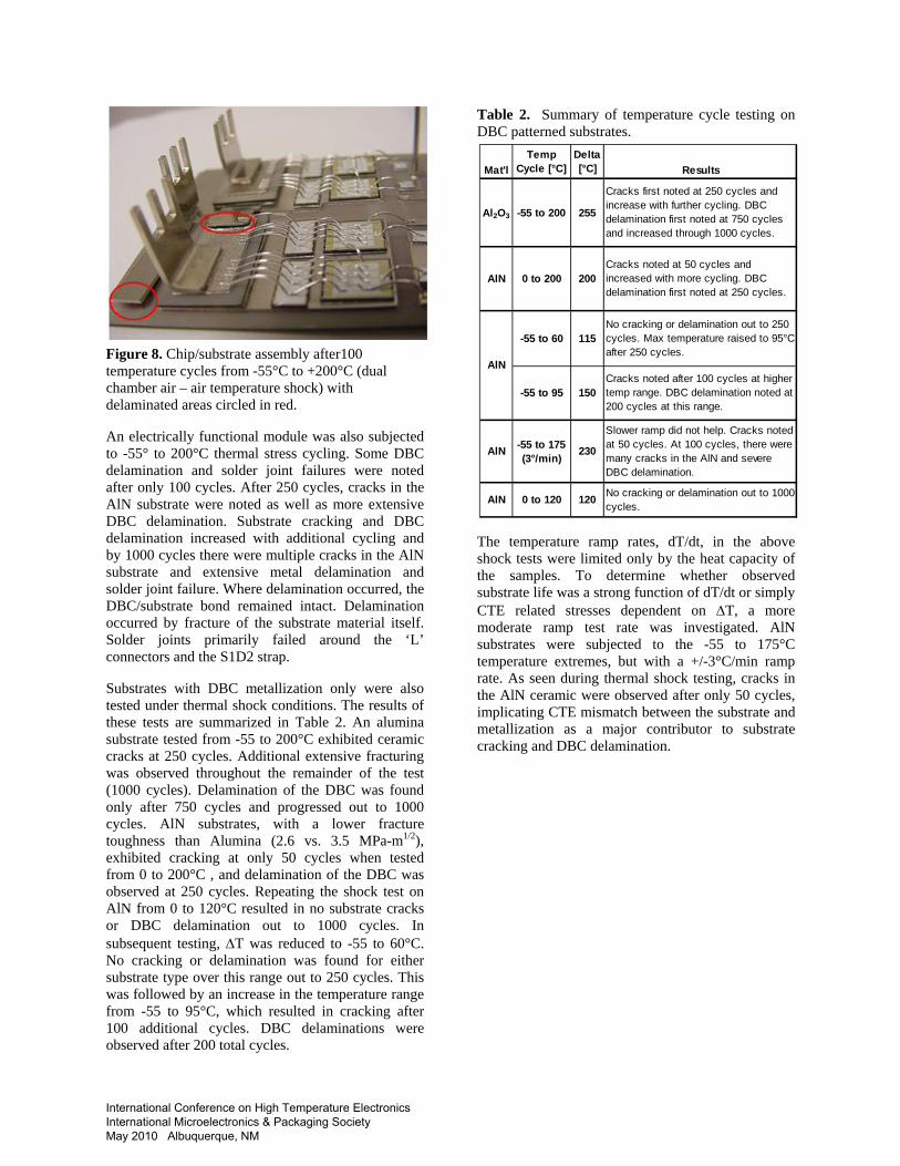
Figure 8. Chip/substrate assembly after100 temperature cycles from -55°C to +200°C (dual chamber air – air temperature shock) with delaminated areas circled in red.
An electrically functional module was also subjected to -55° to 200°C thermal stress cycling. Some DBC delamination and solder joint failures were noted after only 100 cycles. After 250 cycles, cracks in the AlN substrate were noted as well as more extensive DBC delamination. Substrate cracking and DBC delamination increased with additional cycling and by 1000 cycles there were multiple cracks in the AlN substrate and extensive metal delamination and solder joint failure. Where delamination occurred, the DBC/substrate bond remained intact. Delamination occurred by fracture of the substrate material itself. Solder joints primarily failed around the ‘L’ connectors and the S1D2 strap.
Substrates with DBC metallization only were also tested under thermal shock conditions. The results of these tests are summarized in Table 2. An alumina substrate tested from -55 to 200°C exhibited ceramic cracks at 250 cycles. Additional extensive fracturing was observed throughout the remainder of the test (1000 cycles). Delamination of the DBC was found only after 750 cycles and progressed out to 1000 cycles. AlN substrates, with a lower fracture toughness than Alumina (2.6 vs. 3.5 MPa-m1/2), exhibited cracking at only 50 cycles when tested from 0 to 200°C , and delamination of the DBC was observed at 250 cycles. Repeating the shock test on AlN from 0 to 120°C resulted in no substrate cracks or DBC delamination out to 1000 cycles. In subsequent testing, ΔT was reduced to -55 to 60°C. No cracking or delamination was found for either substrate type over this range out to 250 cycles. This was followed by an increase in the temperature range from -55 to 95°C, which resulted in cracking after 100 additional cycles. DBC delaminations were observed after 200 total cycles.
Table 2. Summary of temperature cycle testing on DBC patterned substrates.
The temperature ramp rates, dT/dt, in the above shock tests were limited only by the heat capacity of the samples. To determine whether observed substrate life was a strong function of dT/dt or simply CTE related stresses dependent on ΔT, a more moderate ramp test rate was investigated. AlN substrates were subjected to the -55 to 175°C temperature extremes, but with a +/-3°C/min ramp rate. As seen during thermal shock testing, cracks in the AlN ceramic were observed after only 50 cycles, implicating CTE mismatch between the substrate and metallization as a major contributor to substrate cracking and DBC delamination.
Mat'lTemp
Cycle [°C] Delta [°C] Results
Al2O3 -55 to 200 255
Cracks first noted at 250 cycles and increase with further cycling. DBC delamination first noted at 750 cycles and increased through 1000 cycles.
AlN 0 to 200 200Cracks noted at 50 cycles and increased with more cycling. DBC delamination first noted at 250 cycles.
-55 to 60 115No cracking or delamination out to 250 cycles. Max temperature raised to 95°C after 250 cycles.
-55 to 95 150Cracks noted after 100 cycles at higher temp range. DBC delamination noted at 200 cycles at this range.
AlN -55 to 175 (3°/min)
230
Slower ramp did not help. Cracks noted at 50 cycles. At 100 cycles, there were many cracks in the AlN and severe DBC delamination.
AlN 0 to 120 120 No cracking or delamination out to 1000 cycles.
AlN
International Conference on High Temperature Electronics International Microelectronics & Packaging Society May 2010 Albuquerque, NM

Figure 9. Ceramic substrate with DBC pattern representative of Rev 1A (photograph) and Rev 2 (red outline) from Table 2.
In order to study the stresses related to CTE mismatch, within a given material system, the effects of variations to the DBC pattern and thickness were investigated through numerical modeling and simulation using the FEA software package ALGOR®. Substrate design revision “1A”, shown in Figure 9, is the same as that used on the physical substrates tested previously. The Rev 1A design had 10 mil radiused corners on the top pattern and the backside DBC pattern was a solid rectangle covering most of the backside. The Rev 2 DBC pattern, illustrated in Figure 9 by the red dashed lines, was the same as 1A except that the “L” shaped drain pad region was eliminated. For Rev 2A, the backside DBC pattern was split into two long rectangles. Rev 2AA takes the 2A design and radiuses the corners 60 mil instead of 10 mil. Rev 2BA explores the effects of the backside pattern further by having the backside DBC a mirror image of the front side. Table 3 shows FEA Von Mises stress predictions at the drain DBC pad and maximum substrate bow at 250° and -55°C for several design variations.
Table 3. Results of stress and bow simulations on AlN substrates with DBC pattern, thickness, and corner radius variations.
A slight improvement in bow and stress were seen in going from the Rev 1A to Rev 2 pattern. The split backside DBC pattern of Rev 2A produced a slight improvement in DBC pad stress, but a significant reduction in substrate bow at both 250 and -55°C. Further rounding the pattern corners (Rev 2AA) had a negligible effect. The mirrored bottom DBC pattern of Rev 2BA slightly reduced the Von Mises stress, but almost eliminated wafer bow completely. The effect on thermal impedance and heat sink bond integrity, of the patterned bottom side DBC pattern of Rev 2BA, is being investigated.
Within a given design pattern, reducing the DBC thickness increased the stress in the DBC metal; but significantly reduced the wafer bow. Since the observed DBC delamination failures occurred in the substrate, trading more stress in the metal for reduced bow in the substrate should be a more reliable scenario. However, the benefits of thinner DBC must be weighed against the resulting decrease in electrical conductivity and thermal spreading effectiveness.
Other module design revisions, focused on mitigating the stress-related solder joint failures occurring in the initial Gen II design were also investigated. Figure 10a illustrates a configuration using pin connectors and wirebonds to eliminate the L-shaped connectors and S1D2 strap delamination problem. Another design being pursued uses blade type edge connectors for the source and drain as shown in Figure 10b. For this design 80Au/20Sn, 95Pb/5Sn or 28Cu/72Ag metallurgies will be evaluated for reliability in joining the AlN blades to the substrate.
ItemDesign
Rev.
DBC Thickness
(in)
DBC CornerRadius
(in)
Bottom DBC
Design
Von Mises Drain DBC
Pad (N/mm2)
Max. Bow(mils)
Von Mises Drain DBC
Pad (N/mm2)
Max. Bow(mils)
1 1A 0.012 0.01Full
Coverage 326 -12.0 116 4.3
2 2 0.012 0.01Full
Coverage 325 -11.8 120 4.2
3 2 0.008 0.01Full
Coverage 362 -9.4 128 3.4
4 2 0.005 0.01Full
Coverage 398 -7.9 141 2.85 2A 0.012 0.01 Split 324 -8.3 115 2.96 2A 0.008 0.01 Split 362 -6.7 128 2.37 2A 0.005 0.01 Split 395 -5.1 140 1.98 2AA 0.012 0.06 Split 324 -7.9 115 2.9
9 2BA 0.012 0.06Mirror
Top 318 -0.2 113 0
AlN Substrate Stress and Bow Simulations -55°C250°C
International Conference on High Temperature Electronics International Microelectronics & Packaging Society May 2010 Albuquerque, NM

Figure 10. Module designs featuring a) pin connections and b) blade type edge connections.
Thermal management
In the Gen II design, copper cooling fins are soldered directly to the DBC on the underside of the substrate, as shown in Figure 2. Finite element (FEA) thermal modeling was used to optimize the heatsink parameters of fin height, Cu-thickness, and fin spacing. Figure 11 shows the temperature distribution prediction plot of the FEA modeling results for a geometrically symmetric half-module using an AlN substrate with 0.5” tall, 0.010” thick Cu fins. Inlet air temperature was 0°C and the air flow was 1500 ft/min. Power dissipation assumed to be 100 W per MOSFET and 50 W per JBS diode.
Figure 11. Thermal modeling results for temperature distribution AlN substrate with fins 0.010 in thick, 0.5 in high. Air flow = 1500 ft/min and inlet air = 0°C. Above) 3D, below) cross-section underneath MOSFETs.
Table 4 summarizes these modeling results for modules with AlN substrates and heat sinks with fins 0.5” and 1.0” high, and thickness of 0.008, 0.01, and 0.02”. Power dissipation was assumed to be 100 W per MOSFET and 50 W per JBS diode. For this table, the air flow was kept at 2500 ft/min. Note that as the fin thickness decreases the fin spacing also decreases. Thus, for a fixed fin height, the thinner fins result I greater total fin surface area. However, thinner fins also have a reduced cross-sectional area for conductive heat flow down the length of the fin. For the shorter, 0.5” tall fins, the surface area advantage dominates and the 0.008” thick fins result in the lower peak junction temperature rise. For the 1.0” tall fins, however, heat flow down the fin dominates resulting in the thicker-Cu 0.02” fins producing the lowest junction temperature rise. Working modules will be fabricated and tested using both the 0.008” × 0.5” and the 0.020” × 1.0” fin design to empirically compare to the FEA modeling predicted results.
a)
b)
International Conference on High Temperature Electronics International Microelectronics & Packaging Society May 2010 Albuquerque, NM
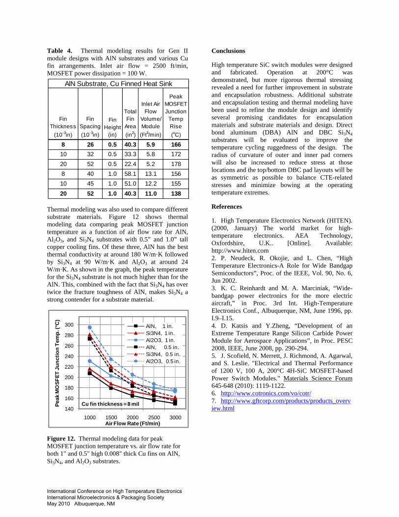
Table 4. Thermal modeling results for Gen II module designs with AlN substrates and various Cu fin arrangements. Inlet air flow = 2500 ft/min, MOSFET power dissipation = 100 W.
Thermal modeling was also used to compare different substrate materials. Figure 12 shows thermal modeling data comparing peak MOSFET junction temperature as a function of air flow rate for AlN, Al2O3, and Si3N4 substrates with 0.5” and 1.0” tall copper cooling fins. Of these three, AlN has the best thermal conductivity at around 180 W/m·K followed by Si3N4 at 90 W/m·K and Al2O3 at around 24 W/m·K. As shown in the graph, the peak temperature for the Si3N4 substrate is not much higher than for the AlN. This, combined with the fact that Si3N4 has over twice the fracture toughness of AlN, makes Si3N4 a strong contender for a substrate material.
Figure 12. Thermal modeling data for peak MOSFET junction temperature vs. air flow rate for both 1" and 0.5" high 0.008" thick Cu fins on AlN, Si3N4, and Al2O3 substrates.
Conclusions
High temperature SiC switch modules were designed and fabricated. Operation at 200°C was demonstrated, but more rigorous thermal stressing revealed a need for further improvement in substrate and encapsulation robustness. Additional substrate and encapsulation testing and thermal modeling have been used to refine the module design and identify several promising candidates for encapsulation materials and substrate materials and design. Direct bond aluminum (DBA) AlN and DBC Si3N4 substrates will be evaluated to improve the temperature cycling ruggedness of the design. The radius of curvature of outer and inner pad corners will also be increased to reduce stress at those locations and the top/bottom DBC pad layouts will be as symmetric as possible to balance CTE-related stresses and minimize bowing at the operating temperature extremes.
References
1. High Temperature Electronics Network (HITEN). (2000, January) The world market for high-temperature electronics. AEA Technology, Oxfordshire, U.K.. [Online]. Available: http://www.hiten.com 2. P. Neudeck, R. Okojie, and L. Chen, “High Temperature Electronics-A Role for Wide Bandgap Semiconductors”, Proc. of the IEEE, Vol. 90, No. 6, Jun 2002. 3. K. C. Reinhardt and M. A. Marciniak, “Wide-bandgap power electronics for the more electric aircraft,” in Proc. 3rd Int. High-Temperature Electronics Conf., Albuquerque, NM, June 1996, pp. I.9–I.15. 4. D. Katsis and Y.Zheng, “Development of an Extreme Temperature Range Silicon Carbide Power Module for Aerospace Applications”, in Proc. PESC 2008, IEEE, June 2008, pp. 290-294. 5. J. Scofield, N. Merrett, J. Richmond, A. Agarwal, and S. Leslie. "Electrical and Thermal Performance of 1200 V, 100 A, 200°C 4H-SiC MOSFET-based Power Switch Modules." Materials Science Forum 645-648 (2010): 1119-1122. 6. http://www.cotronics.com/vo/cotr/ 7. http://www.gftcorp.com/products/products_overview.html
Fin Thickness
(10-3in)
Fin Spacing (10-3in)
Fin Height
(in)
Total Fin
Area (in2)
Inlet Air Flow
Volume/ Module (Ft3/min)
Peak MOSFET Junction
Temp Rise (oC)
8 26 0.5 40.3 5.9 16610 32 0.5 33.3 5.8 17220 52 0.5 22.4 5.2 1788 40 1.0 58.1 13.1 15610 45 1.0 51.0 12.2 15520 52 1.0 40.3 11.0 138
AlN Substrate, Cu Finned Heat Sink
140
160
180
200
220
240
260
280
300
1000 1500 2000 2500 3000
Peak
MO
SFET
Jun
ctio
n Te
mp.
(°C
)
Air Flow Rate (Ft/min)
Cu fin thickness = 8 mil
AlN, 1 in. Si3N4, 1 in.Al2O3, 1 in.AlN, 0.5 in.Si3N4, 0.5 in.Al2O3, 0.5 in.
International Conference on High Temperature Electronics International Microelectronics & Packaging Society May 2010 Albuquerque, NM