Peak) Power Factor Corrected LLC Power Supply Using...
71
Power Integrations 5245 Hellyer Avenue, San Jose, CA 95138 USA. Tel: +1 408 414 9200 Fax: +1 408 414 9201 www.powerint.com Title Reference Design Report for a 225 W (286 W Peak) Power Factor Corrected LLC Power Supply Using HiperPLC (PLC810PG) Specification 90 VAC to 265 VAC Input 225 W (286 W Peak) Total Output Power 5 V SB at 0.5 W 5 V at 9.5 W 12 V at 48 W (60 W Peak) 24 V at 168 W (216 W Peak) Application LCD TV Author Applications Engineering Department Document Number RDR-189 Date February 26, 2009 Revision 1.0.2 Summary and Features • Integrated PFC and LLC controller • Continuous mode PFC using small low-cost EE Sendust core and magnet wire • Frequency and Phase locked PFC and LLC for ripple cancellation in bulk capacitor for reduced ripple current, reduced bulk capacitor and reduced EMI filter cost • Tight LLC duty-cycle matching • Tight LLC dead-time control • Brownout detection circuit • >92% full load PFC efficiency at 90 VAC using conventional ultrafast rectifier • >93% full load LLC efficiency PATENT INFORMATION The products and applications illustrated herein (including transformer construction and circuits external to the products) may be covered by one or more U.S. and foreign patents, or potentially by pending U.S. and foreign patent applications assigned to Power Integrations. A complete list of Power Integrations' patents may be found at www.powerint.com. Power Integrations grants its customers a license under certain patent rights as set forth at <http://www.powerint.com/ip.htm>.
Transcript of Peak) Power Factor Corrected LLC Power Supply Using...

Power Integrations
5245 Hellyer Avenue, San Jose, CA 95138 USA. Tel: +1 408 414 9200 Fax: +1 408 414 9201
www.powerint.com
Title Reference Design Report for a 225 W (286 W Peak) Power Factor Corrected LLC Power Supply Using HiperPLC (PLC810PG)
Specification
90 VAC to 265 VAC Input
225 W (286 W Peak) Total Output Power 5 VSB at 0.5 W 5 V at 9.5 W 12 V at 48 W (60 W Peak) 24 V at 168 W (216 W Peak)
Application LCD TV
Author Applications Engineering Department
Document Number
RDR-189
Date February 26, 2009
Revision 1.0.2
Summary and Features
• Integrated PFC and LLC controller
• Continuous mode PFC using small low-cost EE Sendust core and magnet wire
• Frequency and Phase locked PFC and LLC for ripple cancellation in bulk capacitor for reduced ripple current, reduced bulk capacitor and reduced EMI filter cost
• Tight LLC duty-cycle matching
• Tight LLC dead-time control
• Brownout detection circuit
• >92% full load PFC efficiency at 90 VAC using conventional ultrafast rectifier
• >93% full load LLC efficiency
PATENT INFORMATION
The products and applications illustrated herein (including transformer construction and circuits external to the products) may be covered
by one or more U.S. and foreign patents, or potentially by pending U.S. and foreign patent applications assigned to Power Integrations. A
complete list of Power Integrations' patents may be found at www.powerint.com. Power Integrations grants its customers a license under
certain patent rights as set forth at <http://www.powerint.com/ip.htm>.

RDR-189, 225 W 40 Inch LCD TV Power Supply Using PLC810PG 26-Feb-09
Page 2 of 71
Power Integrations Tel: +1 408 414 9200 Fax: +1 408 414 9201 www.powerint.com
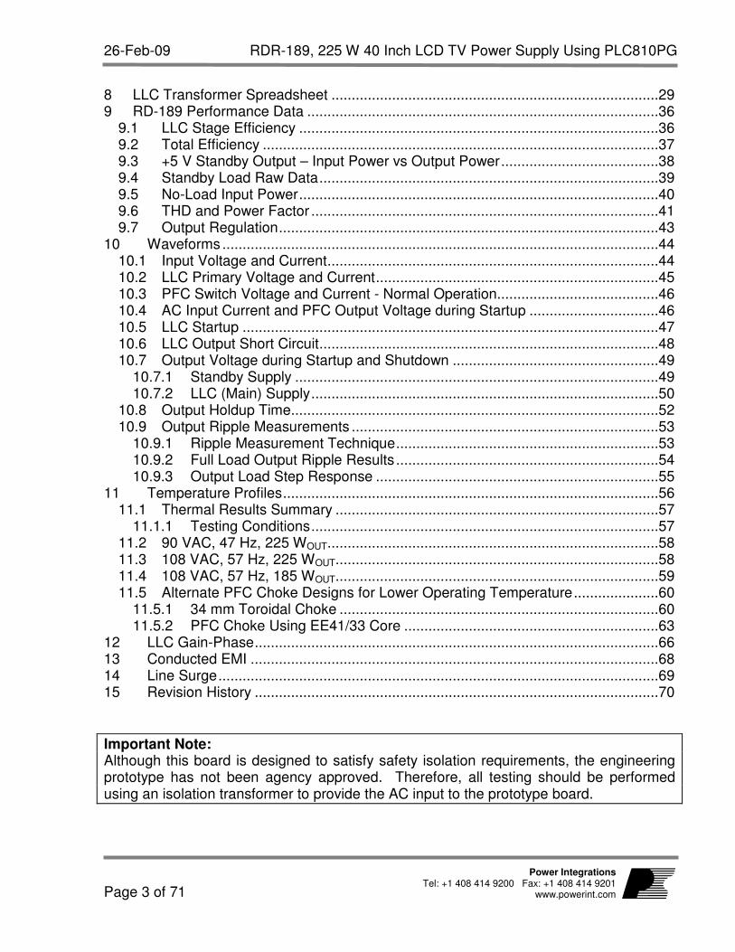
Table of Contents 1 Introduction.................................................................................................................4
2 Power Supply Specification ........................................................................................7
3 Schematic...................................................................................................................8
4 Circuit Description ....................................................................................................11
4.1 Input Filter / Boost Converter.............................................................................11
4.1.1 EMI Filtering ...............................................................................................11
4.1.2 Inrush limiting .............................................................................................11
4.1.3 Main PFC Stage.........................................................................................11
4.2 Main LLC Output ...............................................................................................12
4.2.1 LLC Input Stage .........................................................................................12
4.2.2 LLC Outputs ...............................................................................................12
4.2.3 Switched +5V Output .................................................................................12
4.3 Controller...........................................................................................................12
4.3.1 PFC Control ...............................................................................................12
4.3.2 Bypassing/Ground Isolation .......................................................................13
4.3.3 LLC Control ................................................................................................13
4.4 LLC Secondary Control Circuits ........................................................................13
4.4.1 Voltage Feedback ......................................................................................13
4.5 5 V Standby/Primary Bias Supply/Remote Start................................................13
4.5.1 5 V Flyback Supply.....................................................................................14
4.5.2 Primary Bias regulator/Remote Start..........................................................14
4.5.3 Brownout Shutdown Circuit ........................................................................14
5 PCB Layout ..............................................................................................................15
6 Bill of Materials .........................................................................................................17
7 Magnetics .................................................................................................................22
7.1 Main LLC 12/24 V Transformer (T2) Specification ............................................22
7.1.1 Electrical Diagram ......................................................................................22
7.1.2 Electrical Specifications..............................................................................22
7.2 5V Standby Supply Transformer (T1) Specification) .........................................23
7.2.1 Electrical Diagram ......................................................................................23
7.2.2 Electrical Specifications..............................................................................23
7.2.3 Materials.....................................................................................................23
7.2.4 Build Diagram.............................................................................................24
7.2.5 Construction ...............................................................................................24
7.3 PFC Choke (L4) Specification ...........................................................................25
7.3.1 Electrical Diagram ......................................................................................25
7.3.2 Electrical Specification ...............................................................................25
7.3.3 Materials.....................................................................................................26
7.3.4 Build Diagram.............................................................................................26
7.3.5 Winding Instructions...................................................................................27
7.4 Ground Choke (L3) Specification ......................................................................28
7.4.1 Schematic Diagram....................................................................................28
7.4.2 Materials.....................................................................................................28
7.4.3 Winding Instructions...................................................................................28
26-Feb-09 RDR-189, 225 W 40 Inch LCD TV Power Supply Using PLC810PG
Page 3 of 71
Power Integrations Tel: +1 408 414 9200 Fax: +1 408 414 9201
www.powerint.com
8 LLC Transformer Spreadsheet .................................................................................29
9 RD-189 Performance Data .......................................................................................36
9.1 LLC Stage Efficiency .........................................................................................36
9.2 Total Efficiency ..................................................................................................37
9.3 +5 V Standby Output – Input Power vs Output Power.......................................38
9.4 Standby Load Raw Data....................................................................................39
9.5 No-Load Input Power.........................................................................................40
9.6 THD and Power Factor ......................................................................................41
9.7 Output Regulation..............................................................................................43
10 Waveforms ............................................................................................................44
10.1 Input Voltage and Current..................................................................................44
10.2 LLC Primary Voltage and Current......................................................................45
10.3 PFC Switch Voltage and Current - Normal Operation........................................46
10.4 AC Input Current and PFC Output Voltage during Startup ................................46
10.5 LLC Startup .......................................................................................................47
10.6 LLC Output Short Circuit....................................................................................48
10.7 Output Voltage during Startup and Shutdown ...................................................49
10.7.1 Standby Supply ..........................................................................................49
10.7.2 LLC (Main) Supply......................................................................................50
10.8 Output Holdup Time...........................................................................................52
10.9 Output Ripple Measurements ............................................................................53
10.9.1 Ripple Measurement Technique.................................................................53
10.9.2 Full Load Output Ripple Results .................................................................54
10.9.3 Output Load Step Response ......................................................................55
11 Temperature Profiles.............................................................................................56
11.1 Thermal Results Summary ................................................................................57
11.1.1 Testing Conditions......................................................................................57
11.2 90 VAC, 47 Hz, 225 WOUT..................................................................................58
11.3 108 VAC, 57 Hz, 225 WOUT................................................................................58
11.4 108 VAC, 57 Hz, 185 WOUT................................................................................59
11.5 Alternate PFC Choke Designs for Lower Operating Temperature.....................60
11.5.1 34 mm Toroidal Choke ...............................................................................60
11.5.2 PFC Choke Using EE41/33 Core ...............................................................63
12 LLC Gain-Phase....................................................................................................66
13 Conducted EMI .....................................................................................................68
14 Line Surge.............................................................................................................69
15 Revision History ....................................................................................................70
Important Note: Although this board is designed to satisfy safety isolation requirements, the engineering prototype has not been agency approved. Therefore, all testing should be performed using an isolation transformer to provide the AC input to the prototype board.

RDR-189, 225 W 40 Inch LCD TV Power Supply Using PLC810PG 26-Feb-09
Page 4 of 71
Power Integrations Tel: +1 408 414 9200 Fax: +1 408 414 9201 www.powerint.com
1 Introduction
This engineering report describes a 286 W reference design power supply for flat panel displays (LCD TVs) and also serves as a general purpose evaluation board for the PLC810PG The design is based on the PLC810PG controller IC which integrates both continuous current mode (CCM) boost PFC and resonant half-bridge (LLC) control functions together with a high-side driver for the upper MOSFET of the LLC stage and a low-side LLC driver. RD189 demonstrates a design using the commonly employed single transformer and resonant inductor magnetic component (integrated magnetics) for the LLC stage (common in display applications). However, the PLC810 may as easily be used with separated transformer and resonating inductor. PI design materials support both approaches. The board also includes a standby power supply using a TNY275PN from the TinySwitch-III IC family. This provides the 5 V output during both normal operation and standby.
26-Feb-09 RDR-189, 225 W 40 Inch LCD TV Power Supply Using PLC810PG
Page 5 of 71
Power Integrations Tel: +1 408 414 9200 Fax: +1 408 414 9201
www.powerint.com
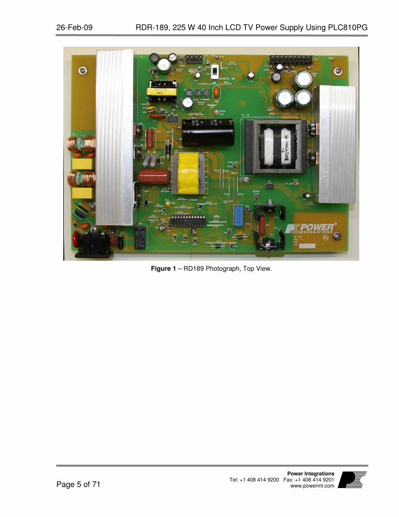
Figure 1 – RD189 Photograph, Top View.

RDR-189, 225 W 40 Inch LCD TV Power Supply Using PLC810PG 26-Feb-09
Page 6 of 71
Power Integrations Tel: +1 408 414 9200 Fax: +1 408 414 9201 www.powerint.com
Figure 2 – RD-189 Photograph, Bottom View.

26-Feb-09 RDR-189, 225 W 40 Inch LCD TV Power Supply Using PLC810PG
Page 7 of 71
Power Integrations Tel: +1 408 414 9200 Fax: +1 408 414 9201
www.powerint.com
2 Power Supply Specification
Description Symbol Min Typ Max Units Comment
Input
Voltage VIN 90 265 VAC 3 Wire input.
Frequency fLINE 47 50/60 64 Hz
Power Factor PF 0.99 Full load, 100/115/230 VAC
No-load Input Power (230 VAC) 0.2 W
No-load Input Power (100/115VAC)
0.08 W
PIN(1 W) 0.6 W For 1 W input power
at 115/230 VAC Available Standby Output Power PIN(2 W) 1.3 W
For 2 W input power at 115/230 VAC
Standby Output
Standby Output Voltage VSB 4.75 5 5.25 V ± 5%
Standby Output Ripple Voltage VRIPPLE(SB) 50 mV 20 MHz bandwidth
Standby Output Current IOUT(SB) 1 A
Main Converter Output
Logic Output Voltage VLG 4.75 5 5.25 V OVPMIN: 115%, OVPMAX: 140%
Logic Output Ripple VRIPPLE(LG) 50 mV 20 MHz bandwidth
Logic Output Current ILG 0 2 2 A
Audio Output Voltage VAU 11 12 13 V OVPMIN: 115%, OVPMAX: 140%
Audio Output Ripple VRIPPLE(AU) 120 mV 20 MHz bandwidth
Audio Output Current IAU 0 4 5 A
Backlight Output Voltage VBL 22 24 26 V OVPMIN: 115%, OVPMAX: 140%
Backlight Output Ripple VRIPPLE(BL) 200 mV 20 MHz bandwidth
Backlight Output Current IBL 0 7 9 A
Total Output Power
Continuous Output Power POUT 225 W Standby + Main
Peak Output Power POUT(PK) 286 W Standby + Main (thermally limited)
Efficiency
Standby at Full Load ηSB 85 % Measured at 115 VAC
Total system at Full Load ηMain 85 87
% Measured at 90 VAC
Measured at 115 VAC / 230 VAC
Environmental
Conducted EMI Meets CISPR22B / EN55022B
Safety Designed to meet IEC950 / UL1950 Class II
Surge Differential Common Mode 100 kHz Ring Wave
2 4 4
kV kV kV
1.2/50 µs surge, IEC 1000-4-5,
Differential Mode: 2 Ω
Common Mode: 12 Ω 500 A short circuit current
Ambient Temperature TAMB 0 50 oC See thermal section for conditions

RDR-189, 225 W 40 Inch LCD TV Power Supply Using PLC810PG 26-Feb-09
Page 8 of 71
Power Integrations Tel: +1 408 414 9200 Fax: +1 408 414 9201 www.powerint.com
3 Schematic
Figure 3 – Schematic of PLC810PG LCD TV Power Supply Application Circuit, Input Circuit and PFC Power Stage.

26-Feb-09 RDR-189, 225 W 40 Inch LCD TV Power Supply Using PLC810PG
Page 9 of 71
Power Integrations Tel: +1 408 414 9200 Fax: +1 408 414 9201
www.powerint.com
Figure 4 –Schematic of PLC810PG LCD TV Power Supply Application Circuit, PFC Circuit Control Inputs and LLC Stage.

RDR-189, 225 W 40 Inch LCD TV Power Supply Using PLC810PG 26-Feb-09
Page 10 of 71
Power Integrations Tel: +1 408 414 9200 Fax: +1 408 414 9201 www.powerint.com
Figure 5 – Schematic of PLC810PG LCD TV Power Supply Application Circuit, Standby Supply.

26-Feb-09 RDR-189, 225 W 40 Inch LCD TV Power Supply Using PLC810PG
Page 11 of 71
Power Integrations Tel: +1 408 414 9200 Fax: +1 408 414 9201
www.powerint.com
4 Circuit Description
The main converter uses the PLC810PG in a primary-side-control, PFC + LLC configuration.
4.1 Input Filter / Boost Converter
The schematic in Figure 3 shows the input EMI filter and main PFC stage.
4.1.1 EMI Filtering
Capacitors C1 and C5 are connected directly across the pins of input receptacle J1 and are used to control common mode noise at frequencies greater than 30MHz. A 5-turn ferrite bead inductor (L3) is used to connect the safety ground from J1 to chassis ground, providing damping at frequencies >30MHz. Common mode inductors L1 and L2 control EMI at low frequencies and the mid-band (~10 MHz), respectively. Capacitors C2 and C6 control resonant peaks in the mid-band (~10 MHz) region. PFC inductor L4 has a grounded shield band to prevent electrostatic and magnetic noise coupling to the EMI filter components. Capacitors C3 and C4 provide differential mode EMI filtering. To meet safety requirements resistors R1, R2 and R3 discharge these capacitors when AC is removed. The heat sink for PFC switch FET Q2 and PFC output diode D2 is tied to primary return at the cathode of D3 to eliminate the heat sink as a source of radiated noise.
4.1.2 Inrush limiting
Thermistor RT1 provides inrush limiting. It is shorted by relay RL1 during normal operation, gated by the power supply remote-on signal, increasing efficiency by approximately 1 - 1.5%.
4.1.3 Main PFC Stage
Components C9, C11, L4, Q2, and D2 form a continuous mode power factor correction circuit. Components Q1, Q3, R4, R9 and bead 2 buffer the PWM drive signal for Q2 from the PLC810 controller. Resistor R4 allows the turn-on speed and R7 the turn-off speed of Q2 to be adjusted to optimize the losses between D2 and Q2. In this design it was found that efficiency and EMI were both improved by reducing the value of R4 and R7 and adding ferrite beads to the gate and drain of Q2 (bead 2 and bead 1 respectively). In general, increasing MOSFET turn on drive current reduces MOSFET switching losses but increases the reverse recovery current through D2 and associated ringing. An ultra fast diode was selected for D2 as a lower cost alternative to a silicon carbide or other proprietary diode technology. These may provide higher efficiency by reducing reverse recovery charge, but significantly increase solution cost.
A 190 mΩ, 500 V power MOSFET was selected for Q2 to maximize the efficiency of the PFC stage.

RDR-189, 225 W 40 Inch LCD TV Power Supply Using PLC810PG 26-Feb-09
Page 12 of 71
Power Integrations Tel: +1 408 414 9200 Fax: +1 408 414 9201 www.powerint.com
Capacitor C10 provides local bypassing for the drive circuit. Current sensing for the PFC stage is provided by R6 and R8. The sense voltage is clamped to two diode drops by D3 and D4 protecting the current sense input of the controller IC during fault conditions. Diode D1 charges the PFC output capacitor (C11) when AC is first applied. This routes the inrush current around the PFC inductor L4 preventing it from saturating and causing stress in Q2 and D2 when the PFC stage begins to operate. Capacitor C11 is used to shrink the high frequency loop around components Q2, D2 and C9 to reduce EMI. The incoming AC is rectified by BR1 and filtered by C7. Capacitor C7 was selected as a low-loss polypropylene type due to its low loss and low impedance characteristics. This capacitor provides the high instantaneous current through L4 during Q2 on-time.
4.2 Main LLC Output
The Figure 4 schematic shows the LLC converter stage and the switched 5 V output, and the controller circuit.
4.2.1 LLC Input Stage
MOSFETs Q10 and Q11 are the switch MOSFETs for the LLC converter. They are driven directly by the controller IC via resistors R56 and R58. Capacitor C39 is the primary resonating capacitor, and should be a low-loss type rated for the RMS current at maximum load. Capacitor C40 is used for local bypassing, and is positioned adjacent to Q10 and Q11. Resistor R59 provides primary current sensing to the controller for overpower protection.
4.2.2 LLC Outputs
The secondaries of transformer T2 are rectified and filtered by D9-10, C37-38 and C53 to provide the +12 V and +24 V outputs. Inductor L8 and C52 provide additional filtering for the 12 V output, removing high frequency noise. Resistor R57 is connected between secondary return and chassis ground for high frequency EMI damping and to tie the secondary return to chassis ground. Capacitors C54 and C55 reduce the loop area for the 12 V and 24 V rectifier circuits.
4.2.3 Switched +5V Output
MOSFET Q12 is used to switch the 5 V output of the standby supply to the +5 V logic output when the main converter is operating. The AC signal from one side of the 12 V output rectifier is used to turn on Q12 via R60, R61, D11, and C43. Capacitor C44 provides filtering of the 5 V logic output and is physically located near the output connection.
4.3 Controller
Figure 4 shows the circuitry around the main controller IC U6, which provides control functions for the input PFC and output LLC stages.
4.3.1 PFC Control
The PFC boost stage output voltage is fed back to the boost voltage sense pin (FBP of U13) via resistors R39-41, R43, R46, and R50. Capacitor C25 filters noise. Components
26-Feb-09 RDR-189, 225 W 40 Inch LCD TV Power Supply Using PLC810PG
Page 13 of 71
Power Integrations Tel: +1 408 414 9200 Fax: +1 408 414 9201
www.powerint.com
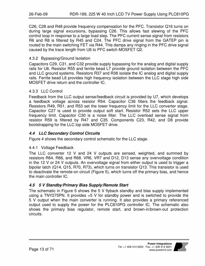
C26, C28 and R48 provide frequency compensation for the PFC. Transistor Q16 turns on during large signal excursions, bypassing C26. This allows fast slewing of the PFC control loop in response to a large load step. The PFC current sense signal from resistors R6 and R8 is filtered by R45 and C24. The PFC drive signal from the GATEP pin is routed to the main switching FET via R44. This damps any ringing in the PFC drive signal caused by the trace length from U6 to PFC switch MOSFET Q2.
4.3.2 Bypassing/Ground Isolation
Capacitors C29, C31, and C32 provide supply bypassing for the analog and digital supply rails for U6. Resistor R55 and ferrite bead L7 provide ground isolation between the PFC and LLC ground systems. Resistors R37 and R38 isolate the IC analog and digital supply rails. Ferrite bead L6 provides high frequency isolation between the LLC stage high side MOSFET drive return and the controller IC.
4.3.3 LLC Control
Feedback from the LLC output sense/feedback circuit is provided by U7, which develops a feedback voltage across resistor R54. Capacitor C36 filters the feedback signal. Resistors R49, R51, and R53 set the lower frequency limit for the LLC converter stage. Capacitor C27 is used to provide output soft start. Resistor R52 sets the LLC upper frequency limit. Capacitor C30 is a noise filter. The LLC overload sense signal from resistor R59 is filtered by R47 and C35. Components C23, R42, and D8 provide bootstrapping for the LLC top side MOSFET drive.
4.4 LLC Secondary Control Circuits
Figure 4 shows the secondary control schematic for the LLC stage.
4.4.1 Voltage Feedback
The LLC converter 12 V and 24 V outputs are sensed, weighted, and summed by resistors R64, R66, and R68. VR6, VR7 and D12, D13 sense any overvoltage condition in the 12 V or 24 V outputs. An overvoltage signal from either output is used to trigger a bipolar latch (Q14, Q15, R70, R73), which turns on transistor Q13. This transistor is used to deactivate the remote-on circuit (Figure 5), which turns off the primary bias, and hence the main controller IC.
4.5 5 V Standby/Primary Bias Supply/Remote Start
The schematic in Figure 5 shows the 5 V flyback standby and bias supply implemented using a TNY275PN. It provides +5 V for standby power and is switched to provide the 5 V output when the main converter is running. It also provides a primary referenced output used to supply the power for the PLC810PG controller IC. The schematic also shows the primary bias regulator, remote start, and brown-in/brown-out protection circuits.

RDR-189, 225 W 40 Inch LCD TV Power Supply Using PLC810PG 26-Feb-09
Page 14 of 71
Power Integrations Tel: +1 408 414 9200 Fax: +1 408 414 9201 www.powerint.com
4.5.1 5 V Flyback Supply
A TNY275PN (U4) is used in a single-ended Flyback supply to provide +5 V output and primary bias. Components VR1, R10, C12, and D5 clamp the primary leakage spike. This Zener-type clamp was selected over a RCD type for low standby power consumption. Resistor R11 sets the standby supply turn-on threshold to approximately 80 VAC. Components VR5, U2, R27, and R33 are used for overvoltage shutdown protection during an open loop fault condition. Components U3, R13, R17, R18, R23, C18 and C19 are the secondary output sensing and feedback components. Capacitor C13 is used for local primary bypassing for the flyback converter. Resistor R12 provides sufficient bias to U4 to turn off its internal HV bias supply, reducing low load and no-load power consumption. Capacitor C42 reduces common mode EMI.
4.5.2 Primary Bias regulator/Remote Start
Components Q4, Q5, Q8, VR2, U1, C17, C51 R14, R16, R20, and SW1 constitute the bias regulator and remote on-off functions. Darlington transistor Q4, R14, and VR2 form a simple emitter-follower voltage regulator that is switched via optocoupler U1. Capacitor C17 limits the rate of rise of the bias voltage to avoid triggering the current limit of the standby supply. Components Q5, C51, and R20 quickly discharge C17 when optocoupler U1 is turned off. Optocoupler U1 is turned on and off by Q8, SW1, R34, and R36. The supply can also be turned on by shorting test points TP5 and TP7.
4.5.3 Brownout Shutdown Circuit
A brownout shutdown circuit is provided. This circuit operates by sensing the AC input voltage and the presence of a switching signal from the LLC controller. When the power supply is operating, the absence of both of these signals, indicating insufficient AC input voltage and insufficient B+ voltage at the input to the LLC converter stage will cause the supply to shut down by switching off the primary bias regulator. Components R24, R26, R28-30, C21, VR4, and Q7 are used to sense The AC input voltage. The voltage threshold of this circuit is set below the turn-on threshold of the standby/primary bias converter. Sufficient AC voltage triggers Q7, discharging capacitor C22, which is charged via R15. Resistor R25 provides some hysteresis to prevent chattering around the AC threshold voltage. Components R32, R35, and Q9 sense the switching drive from the lower output FET of the LLC converter. Transistor Q9 discharges capacitor C22 when the switching signal is present. When the input voltage is sufficiently low, Q7 and Q9 turn off, allowing C22 to charge. Components Q6, R21, and VR3 sense the voltage at C22. When C22 has charged sufficiently, Q6 turns on, turning off the primary bias supply via Q4 and Q5, shutting down the PFC and LLC stages.

26-Feb-09 RDR-189, 225 W 40 Inch LCD TV Power Supply Using PLC810PG
Page 15 of 71
Power Integrations Tel: +1 408 414 9200 Fax: +1 408 414 9201
www.powerint.com
5 PCB Layout
Figure 6 – Printed Circuit Layout, Top Side.

RDR-189, 225 W 40 Inch LCD TV Power Supply Using PLC810PG 26-Feb-09
Page 16 of 71
Power Integrations Tel: +1 408 414 9200 Fax: +1 408 414 9201 www.powerint.com
Figure 7 – Printed Circuit Layout, Bottom Side.

26-Feb-09 RDR-189, 225 W 40 Inch LCD TV Power Supply Using PLC810PG
Page 17 of 71
Power Integrations Tel: +1 408 414 9200 Fax: +1 408 414 9201
www.powerint.com
6 Bill of Materials
Item Qty Ref Des
Description Mfg Part Number Mfg
1 2 BEAD1 BEAD2
3.5 mm D x 3.25 L mm, 21 Ω at 25 MHz, 1.6mm (.063) hole, Ferrite Bead 2643001501 Fair-Rite
2 3 BEAD3 L6
L7 3.5 mm x 4.45 mm, 68 Ω at 100 MHz, 22 AWG hole, Ferrite Bead 2743001112 Fair-Rite
3 1 BR1 600 V, 8 A, Bridge Rectifier, GBJ Package GBJ806-F Diodes, Inc.
4 4 C1 C2 C5
C6 330 pF, Ceramic Y1 440LT33-R Vishay
5 2 C3 C4 470 nF, 275 VAC, Film, X2 PX474K31D5 Carli
6 1 C7 1 µF, 630 V, Polypropylene Film ECW-F6105HL Panasonic
7 1 C9 220 µF, 450 V, Electrolytic, (25 x 45) ECO-S2WP221CX Panasonic
8 6
C10 C17 C23 C27 C31 C33 1 µF, 25 V, Ceramic, X7R, 1206 ECJ-3YB1E105K Panasonic
9 2 C11 C13 20 nF, 500 V, Disc Ceramic D203Z59Z5UL63L0R Vishay/BC
10 1 C12 1 nF, 1 kV, Disc Ceramic DEBE33A102ZC1B Murata
11 1 C14
2200 µF, 10 V, Electrolytic, Very Low ESR,
21 mΩ, (12.5 x 20) EKZE100ELL222MK20S Nippon Chemi-Con
12 1 C15 220 µF, 25 V, Electrolytic, Gen. Purpose, (8 x 11.5) EKMG250ELL221MHB5D Nippon Chemi-Con
13 1 C16 470 µF, 35 V, Electrolytic, Low ESR, 52 m Ω, (10 x 20) ELXZ350ELL471MJ20S Nippon Chemi-Con
14 4 C18 C20 C22 C32 100 nF, 50 V, Ceramic, X7R, 1206 ECJ-3VB1H104K Panasonic
15 4 C19 C26 C29 C43
10 µF, 50 V, Electrolytic, Gen. Purpose, (5 x 11) EKMG500ELL100ME11D Nippon Chemi-Con
16 6
C21 C24 C30 C34 C35 C36 1 nF, 50 V, Ceramic, X7R, 0805 ECJ-2VB1H102K Panasonic
17 2 C25 C49 10 nF, 50 V, Ceramic, X7R, 0805 ECJ-2VB1H103K Panasonic
18 3 C28 C45
C47 22 nF, 50 V, Ceramic, X7R, 0805 ECJ-2VB1H223K Panasonic
19 3 C37 C38
C53
1800 µF, 35 V, Electrolytic, Very Low ESR,
16 mΩ, (16 x 25) EKZE350ELL182ML25S Nippon Chemi-Con
20 1 C39 22 nF, 1250 V, Film B32652A7223J Epcos
21 1 C40 100 nF, 630 V, Film ECQ-E6104KF Panasonic
22 1 C42 1 nF, Ceramic, Y1 440LD10-R Vishay
23 1 C44 10 uF, 25 V, Ceramic, X7R, 1206 ECJ-3YB1E106M Panasonic
24 1 C46 2.2 nF, 50 V, Ceramic, X7R, 0805 ECJ-2VB1H222K Panasonic
25 1 C48 1 µF, 50 V, Electrolytic, Gen. Purpose, (5 x 11) EKMG500ELL1R0ME11D Nippon Chemi-Con
26 1 C50 220 nF, 25 V, Ceramic, X7R, 1206 ECJ-3VB1E224K Panasonic
27 1 C51 100 pF, 100 V, Ceramic, COG, 0805 C0805C101J1GACTU Kemet
28 1 C52 100 µF, 35 V, Electrolytic, Low ESR, 180 mΩ, (6.3 x 15) ELXZ350ELL101MF15D Nippon Chemi-Con
29 1 D1 600 V, 3 A, Recitifier, DO-201AD 1N5406 Vishay
30 1 D2 600 V, 8 A, Ultrafast Recovery, 12 ns, TO-220AC STTH8S06D ST Semiconductor
31 2 D3 D14 1000 V, 1 A, Rectifier, DO-41 1N4007-E3/54 Vishay
32 2 D4 D15 1000 V, 1 A, Rectifier, Glass Passivated, DO-213AA (MELF) DL4007-13-F Diodes Inc
33 1 D5 1000 V, 1 A, Ultrafast Recovery, 75 ns, DO-41 UF4007-E3 Vishay

RDR-189, 225 W 40 Inch LCD TV Power Supply Using PLC810PG 26-Feb-09
Page 18 of 71
Power Integrations Tel: +1 408 414 9200 Fax: +1 408 414 9201 www.powerint.com
34 1 D6 40 V, 5 A, Schottky, DO-201AD SB540 Vishay
35 1 D7 200 V, 1 A, Ultrafast Recovery, 50 ns, DO-41 UF4003-E3 Vishay
36 1 D8 600 V, 1 A, Ultrafast Recovery, 75 ns, DO-41 UF4005-E3 Vishay
37 2 D9 D10 100 V, 16 A, Dual Schottky, TO-220AB 16CTT100 Vishay
38 6
D11 D12 D13 D16 D17 D18 75 V, 0.15 A, Fast Switching, 4 ns, MELF LL4148-13 Diode Inc.
39 1 F1 5 A, 250 V, Slow, TR5 3721500041 Wickman
40 1 GREASE1 Thermal Grease, Silicone, 5 oz Tube CT40-5 ITW Chemtronics
41 4
HS PAD1 HS PAD2 HS PAD3 HS PAD4 HEATSINK PAD, TO-220, Sil-Pad K10 K10-58 Bergquist
42 1 HS1 HEATSINK, Alum, EXT, 3 hole, 3 mtg holes, 6.00" L x 1.150" W x 1.300" H 62230U06000G,MOD Aavid
43 2 HS2 HS3 HEATSINK, TWISTED FIN, 13.4°C/Watt, TO-220 593002B03400G AavidThermalloy
44 1 HS4 HEATSINK, Alum, EXT, 2 hole, 2 mtg holes,4.00" L x 1.150" W x 1.300" H 62230U04000G,MOD Aavid
45 1 J1 AC Input Receptacle and Accessory Plug, PCBM 161-R301SN13 Kobiconn
46 1 J3 10 Position (1 x 10) header, 0.156 pitch, Vertical 26-48-1105 Molex
47 1 J4 4 Position (1 x 4) header, 0.156 pitch, Vertical 26-48-1045 Molex
48 15
JP1 JP2 JP3 JP4 JP5 JP6 JP7 JP8
JP9 JP10 JP11 JP12 JP13 JP14
JP15 Wire Jumper, Non insulated, 22 AWG, 0.4 in 298 Alpha
49 5
JP16 JP17 JP18 JP19
JP36 Wire Jumper, Non insulated, 22 AWG, 0.6 in 298 Alpha
50 4
JP20 JP21 JP_C9+ JP_C9- Wire Jumper, Non insulated, 22 AWG, 0.7 in 298 Alpha
51 9
JP22 JP23 JP24 JP26 JP27 JP28 JP29 JP30
JP37 Wire Jumper, Non insulated, 22 AWG, 0.8 in 298 Alpha
52 4 JP31 JP32 JP33 JP34 Wire Jumper, Non insulated, 22 AWG, 1.3 in 298 Alpha
53 1 JP35 Wire Jumper, Non insulated, 22 AWG, 1.4 in 298 Alpha
54 2 L1 L2 Common Mode Choke Toroidal, 10 mH T22148-902S Fontaine Tech CO. LTD
55 1 L3 29 µH, Ground Choke, Flying Lead
56 1 L4 PFC Choke, EE35/28, horizontal, 480 uH
57 2 L5 L8 3.3 uH, 5.5 A RL622-3R3K-RC JW Miller
58 2 NUT1 NUT2 Nut, Hex, Kep 4-40, S ZN Cr3 plateing RoHS 4CKNTZR Olander
59 1 Q1 NPN,60V 1000MA, SOT-23 FMMT491TA Zetex Inc

26-Feb-09 RDR-189, 225 W 40 Inch LCD TV Power Supply Using PLC810PG
Page 19 of 71
Power Integrations Tel: +1 408 414 9200 Fax: +1 408 414 9201
www.powerint.com
60 1 Q2 560 V, 21 A, 190 mOhm. N-Channel, TO-220 SPP21N50C3IN Infineon
61 1 Q3 PNP, 60V 1000MA, SOT-23 FMMT591TA Zetex Inc
62 1 Q4 NPN, DARL 80V 500MA, SOT-89 BST52TA Zetex Inc
63 3 Q5 Q13
Q14 PNP, Small Signal BJT, 40 V, 0.2 A, SOT-23 MMBT3906LT1G On Semiconductor
64 5 Q6 Q7 Q8 Q9 Q15 NPN, Small Signal BJT, 40 V, 0.2 A, SOT-23 MMBT3904LT1G On Semiconductor
65 2 Q10 Q11 500 V, 4.7 A, 670 mOhm. N-Channel, TO-220FP IRFIB5N50LPBF IR/Vishay
66 1 Q12 20 V, 14 A, 4.5 mOhm, N-Channel, SO-8 SI4408DY-T1-E3 Vishay
67 1 Q16 PNP, Small Signal BJT, 40 V, 0.2 A, TO-92 2N3906G On Semiconductor
68 5 R1 R2 R3 R29 R30 680 kΩ, 5%, 1/4 W, Metal Film, 1206 ERJ-8GEYJ684V Panasonic
69 1 R4 0 Ω, 5%, 1/4 W, Metal Film, 1206 ERJ-8GEY0R00V Panasonic
70 2 R6 R8 0.11 Ω, 5%, 2 W, Metal Oxide MO200J0R11B Synton-Tech corporation
71 1 R7 2.2 Ω, 5%, 1/4 W, Metal Film, 1206 ERJ-8GEYJ2R2V Panasonic
72 1 R9 4.7 kΩ, 5%, 1/4 W, Metal Film, 1206 ERJ-8GEYJ472V Panasonic
73 1 R10 220 kΩ, 5%, 1/2 W, Carbon Film CFR-50JB-220K Yageo
74 1 R11 4.7 MΩ, 5%, 1/2 W, Carbon Film CFR-50JB-4M7 Yageo
75 3 R12 R14
R16 22 kΩ, 5%, 1/4 W, Metal Film, 1206 ERJ-8GEYJ223V Panasonic
76 2 R13 R22 470 Ω, 5%, 1/4 W, Metal Film, 1206 ERJ-8GEYJ471V Panasonic
77 1 R15 330 kΩ, 5%, 1/4 W, Metal Film, 1206 ERJ-8GEYJ334V Panasonic
78 7
R17 R33 R36 R47 R63 R65
R72 1 kΩ, 5%, 1/4 W, Metal Film, 1206 ERJ-8GEYJ102V Panasonic
79 1 R18 10.2 kΩ, 1%, 1/4 W, Metal Film, 1206 ERJ-8ENF1022V Panasonic
80 1 R19 1.3 MΩ, 5%, 1/4 W, Metal Film, 1206 ERJ-8GEYJ135V Panasonic
81 1 R20 220 kΩ, 5%, 1/4 W, Metal Film, 1206 ERJ-8GEYJ224V Panasonic
82 2 R21 R26 100 kΩ, 5%, 1/4 W, Metal Film, 1206 ERJ-8GEYJ104V Panasonic
83 2 R23 R68 10.0 kΩ, 1%, 1/4 W, Metal Film, 1206 ERJ-8ENF1002V Panasonic
84 1 R24 226 kΩ, 1%, 1/4 W, Metal Film, 1206 ERJ-8ENF2263V Panasonic
85 1 R25 3.9 MΩ, 5%, 1/4 W, Metal Film, 1206 ERJ-8GEYJ395V Panasonic
86 1 R27 33 Ω, 5%, 1/4 W, Metal Film, 1206 ERJ-8GEYJ330V Panasonic
87 1 R28 620 kΩ, 5%, 1/4 W, Metal Film, 1206 ERJ-8GEYJ624V Panasonic
88 1 R31 2.2 kΩ, 5%, 1/4 W, Metal Film, 1206 ERJ-8GEYJ222V Panasonic
89 7
R32 R35 R61 R69 R70 R73
R74 10 kΩ, 5%, 1/4 W, Metal Film, 1206 ERJ-8GEYJ103V Panasonic
90 2 R34 R62 3.9 kΩ, 5%, 1/4 W, Metal Film, 1206 ERJ-8GEYJ392V Panasonic
91 2 R37 R38 4.7 Ω, 5%, 1/4 W, Metal Film, 1206 ERJ-8GEYJ4R7V Panasonic
92 5
R39 R40 R41 R43
R46 768 kΩ, 1%, 1/4 W, Metal Film, 1206 ERJ-8ENF7683V Panasonic
93 4 R42 R44 R56 R58 10 Ω, 5%, 1/4 W, Metal Film, 1206 ERJ-8GEYJ100V Panasonic
94 1 R45 150 Ω, 5%, 1/4 W, Metal Film, 1206 ERJ-8GEYJ151V Panasonic
95 1 R48 2.2 kΩ, 5%, 1/8 W, Carbon Film CFR-12JB-2K2 Yageo
96 1 R49 51.1 kΩ, 1%, 1/4 W, Metal Film, 1206 ERJ-8ENF5112V Panasonic
97 2 R50 R51 22.1 kΩ, 1%, 1/4 W, Metal Film, 1206 ERJ-8ENF2212V Panasonic
RDR-189, 225 W 40 Inch LCD TV Power Supply Using PLC810PG 26-Feb-09
Page 20 of 71
Power Integrations Tel: +1 408 414 9200 Fax: +1 408 414 9201 www.powerint.com
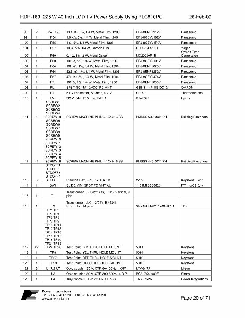
98 2 R52 R53 19.1 kΩ, 1%, 1/4 W, Metal Film, 1206 ERJ-8ENF1912V Panasonic
99 1 R54 1.8 kΩ, 5%, 1/4 W, Metal Film, 1206 ERJ-8GEYJ182V Panasonic
100 1 R55 1 Ω, 5%, 1/4 W, Metal Film, 1206 ERJ-8GEYJ1R0V Panasonic
101 1 R57 10 Ω, 5%, 1/4 W, Carbon Film CFR-25JB-10R Yageo
102 1 R59 0.1 Ω, 5%, 2 W, Metal Oxide MO200J0R1B Synton-Tech Corporation
103 1 R60 100 Ω, 5%, 1/4 W, Metal Film, 1206 ERJ-8GEYJ101V Panasonic
104 1 R64 162 kΩ, 1%, 1/4 W, Metal Film, 1206 ERJ-8ENF1623V Panasonic
105 1 R66 82.5 kΩ, 1%, 1/4 W, Metal Film, 1206 ERJ-8ENF8252V Panasonic
106 1 R67 470 kΩ, 5%, 1/4 W, Metal Film, 1206 ERJ-8GEYJ474V Panasonic
107 1 R71 100 Ω, 1%, 1/4 W, Metal Film, 1206 ERJ-8ENF1000V Panasonic
108 1 RL1 SPST-NO, 5A 12VDC, PC MNT G6B-1114P-US-DC12 OMRON
109 1 RT1 NTC Thermistor, 5 Ohms, 4.7 A CL150 Thermometrics
110 1 RV1 320V, 84J, 15.5 mm, RADIAL S14K320 Epcos
111 5
SCREW1 SCREW2 SCREW3 SCREW4 SCREW18 SCREW MACHINE PHIL 6-32X5/16 SS PMSSS 632 0031 PH Building Fasteners
112 12
SCREW5 SCREW6 SCREW7 SCREW8 SCREW9 SCREW10 SCREW11 SCREW12 SCREW13 SCREW14 SCREW15 SCREW16 SCREW MACHINE PHIL 4-40X5/16 SS PMSSS 440 0031 PH Building Fasteners
113 5
STDOFF1 STDOFF2 STDOFF3 STDOFF4 STDOFF5 Standoff Hex,6-32, .375L,Alum 2209 Keystone Elect
114 1 SW1 SLIDE MINI SPDT PC MNT AU 1101M2S3CBE2 ITT Ind/C&Kdiv
115 1 T1 Transformer, 5V Stby/Bias, EE25, Vertical, 9 pins
116 1 T2 Transformer, LLC, 12/24V, EX4841, Horizontal, 14 pins SRX48EM-P241200H8701 TDK
117 22
TP1 TP2 TP3 TP4 TP5 TP6 TP7 TP9
TP10 TP11 TP12 TP13 TP14 TP15 TP16 TP17 TP18 TP20 TP21 TP23 TP24 TP26 Test Point, BLK,THRU-HOLE MOUNT 5011 Keystone
118 1 TP8 Test Point, YEL,THRU-HOLE MOUNT 5014 Keystone
119 1 TP27 Test Point, RED,THRU-HOLE MOUNT 5010 Keystone
120 1 TP28 Test Point, ORG,THRU-HOLE MOUNT 5013 Keystone
121 3 U1 U2 U7 Opto coupler, 35 V, CTR 80-160%, 4-DIP LTV-817A Liteon
122 1 U3 Opto coupler, 80 V, CTR 300-600%, 4-DIP PC817X4J000F Sharp
123 1 U4 TinySwitch-III, TNY275PN, DIP-8C TNY275PN Power Integrations

26-Feb-09 RDR-189, 225 W 40 Inch LCD TV Power Supply Using PLC810PG
Page 21 of 71
Power Integrations Tel: +1 408 414 9200 Fax: +1 408 414 9201
www.powerint.com
124 2 U5 U8 IC, REG ZENER SHUNT ADJ SOT-23 LM431AIM3/NOPB National Semiconductor
125 1 U6 Controller, PFC/LLC, 24-pin DIP PLC810PG Power Integrations
126 1 VR1 150 V, 5 W, 5%, TVS, DO204AC (DO-15) P6KE150A LittlelFuse
127 2 VR2 VR7 15 V, 5%, 500 mW, DO-213AA (MELF) ZMM5245B-7 Diodes Inc
128 1 VR3 5.6 V, 5%, 500 mW, DO-213AA (MELF) ZMM5232B-7 Diodes Inc
129 1 VR4 10 V, 5%, 500 mW, DO-213AA (MELF) ZMM5240B-7 Diodes Inc
130 1 VR5 5.1 V, 5%, 500 mW, DO-213AA (MELF) ZMM5231B-7 Diodes Inc
131 1 VR6 30 V, 5%, 500 mW, DO-213AA (MELF) ZMM5256B-7 Diodes Inc
132 5
WASHER1 WASHER2 WASHER3 WASHER4 WASHER18 Washer Flat #6, SS FWSS 006 Building Fasteners
133 12
WASHER5 WASHER6 WASHER7 WASHER8 WASHER9 WASHER10 WASHER11 WASHER12 WASHER13 WASHER14 WASHER15 WASHER16 WASHER FLAT #4 SS FWSS 004 Building Fasteners
134 4
WASHER17 WASHER18 WASHER19 WASHER20 Washer Nylon Shoulder #4 3049 Keystone
135 1 Printed Circuit board, RD189, Rev. K
RDR-189, 225 W 40 Inch LCD TV Power Supply Using PLC810PG 26-Feb-09
Page 22 of 71
Power Integrations Tel: +1 408 414 9200 Fax: +1 408 414 9201 www.powerint.com
7 Magnetics
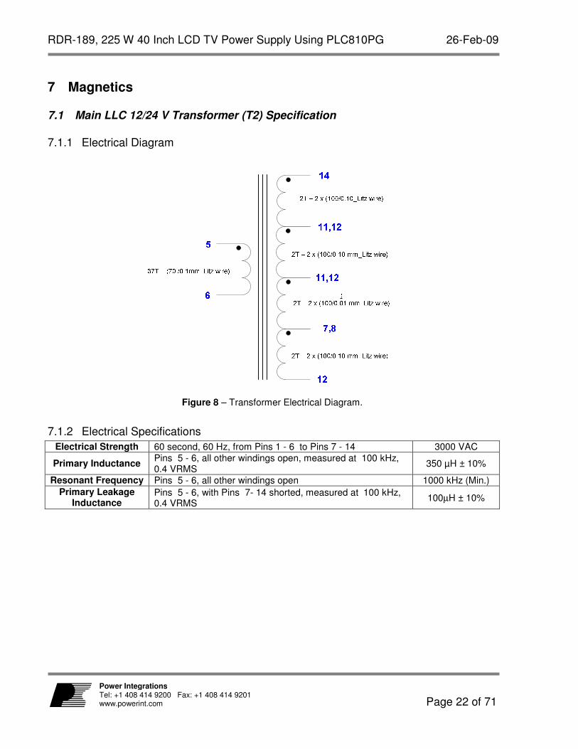
7.1 Main LLC 12/24 V Transformer (T2) Specification
7.1.1 Electrical Diagram
Figure 8 – Transformer Electrical Diagram.
7.1.2 Electrical Specifications
Electrical Strength 60 second, 60 Hz, from Pins 1 - 6 to Pins 7 - 14 3000 VAC
Primary Inductance Pins 5 - 6, all other windings open, measured at 100 kHz, 0.4 VRMS
350 µH ± 10%
Resonant Frequency Pins 5 - 6, all other windings open 1000 kHz (Min.)
Primary Leakage Inductance
Pins 5 - 6, with Pins 7- 14 shorted, measured at 100 kHz, 0.4 VRMS
100µH ± 10%

26-Feb-09 RDR-189, 225 W 40 Inch LCD TV Power Supply Using PLC810PG
Page 23 of 71
Power Integrations Tel: +1 408 414 9200 Fax: +1 408 414 9201
www.powerint.com
7.2 5V Standby Supply Transformer (T1) Specification)
7.2.1 Electrical Diagram
63T – #35 AWG
52T – #35 AWG
7T 2 x #25 AWG_TIWWD1
WD2
WD3
WD4
19T – 2 X #35 AWG
1
2
3
4
5
9,10
6,7
Figure 9 – Standby Transformer Schematic.
7.2.2 Electrical Specifications
Electrical Strength 1 second, 60Hz, from Pins 1-5 to Pins 6-10 3000 VAC
Primary Inductance Pin 1-3 , all other winding open, measured at 100 KHz, 0.4 VRMS
4.41 mH, ± 10%
Resonant Frequency Pin 1-3, all other winding open 800 KHz (min)
Primary Leakage Inductance
Pins 1-3, with Pins 6- 10 shorted, , measured at 100 KHz, 0.4 VRMS
45 µH (max)
7.2.3 Materials
Item Description
[1] Core Pair: EE25, Nippon Ceramic NC-2H or equivalent, gapped for AL of 333 nH/T2.
[2] Bobbin: EE25, Phenolic, Vertical, 10 pins, (5/5), Yih Hwa YW360-02B or equivalent. [3] Magnet Wire: #35 AWG, solderable double coated. [4] Triple Insulated Wire: 25AWG, Furukawa Tex-E or equivalent. [5] Tape: Polyester Film 3M 1350F-1 or equivalent, 10.6 mm wide. [6] Transformer Varnish, Dolph, BC-359-MS or equivalent.
RDR-189, 225 W 40 Inch LCD TV Power Supply Using PLC810PG 26-Feb-09
Page 24 of 71
Power Integrations Tel: +1 408 414 9200 Fax: +1 408 414 9201 www.powerint.com
7.2.4 Build Diagram
3
2
6,7
9,10
4
5
2
1
63T – #35 AWG
7T 2 x #25AWG_TIW
52T – #35 AWG
WD1 (1st half Primary)
WD2 (Secondary)
WD3 (Bias) 19T – 2 X #35 AWG
WD4 (2nd half Primary)
Figure 10 – Standby Transformer Build Diagram.
7.2.5 Construction
Winding/Bobbin preparation
Orient bobbin (item [2]) on winding machine such that the pin side of bobbin is on the left side. Remove Pin 8.
WD1 (1
st half
Primary)
Starting at pin 3, wind 63 turns of wire item [3] in one layer from left to right. After the last turn, place ½” piece of tape item [7] on winding to insulate the crossover, and bring the wire back to the left side to terminate at pin 2.
Insulation Apply two layers of tape (item [5]). WD2
(Secondary) Starting at pins 9&10, wind 7 bifilar turns of triple insulated wire (item [4]) in one layer, from left to right, finishing at pins 6&7.
Insulation Apply two layers of tape (item [5]).
WD3 (Bias)
Staring at pin 4, wind 19 bifilar turns of wire (item [3]) in one layer from left to right, spreading turns evenly across the bobbin, finishing at pin 5.
Insulation Apply one layer of tape (item [5]).
WD4 (2
nd half
Primary)
Starting at pin 2, wind 52 turns of wire (item [3]) from left to right in one layer, spreading the turns evenly across the bobbin. After the last turn, use ½” of tape (item [5]) to insulate finish lead crossover, and finish at pin 1.
Insulation Apply 3 layers of tape (item [5]) as finish wrap.
Finish Gap core halves (item [1]) for inductance of 4.41 mH +/-10%. Assemble and secure core halves. Dip varnish using (item [6]).

26-Feb-09 RDR-189, 225 W 40 Inch LCD TV Power Supply Using PLC810PG
Page 25 of 71
Power Integrations Tel: +1 408 414 9200 Fax: +1 408 414 9201
www.powerint.com
7.3 PFC Choke (L4) Specification
7.3.1 Electrical Diagram
Figure 11 – PFC Choke Schematic.
7.3.2 Electrical Specification
Inductance: 480 µH ± 15%
Note – Do not measure inductance without copper strap (shield) in place!

RDR-189, 225 W 40 Inch LCD TV Power Supply Using PLC810PG 26-Feb-09
Page 26 of 71
Power Integrations Tel: +1 408 414 9200 Fax: +1 408 414 9201 www.powerint.com
7.3.3 Materials
Item Description [1] E Core Pair: Sendust, 60µ, EE35/28 Chang Sung S060 EE35/28 or equivalent. [2] Bobbin, E375, Horizontal, 12 pin, Ferroxcube CPH-E34/14/9-1S-12PD-Z or equivalent. [3] Magnet Wire: #24AWG, solderable double coated. [4] Tape Polyester Film, 3M 1350F-1 or equivalent, 17 mm wide. [5] Tape Polyester Film, 3M 1350F-1 or equivalent, 9 mm wide. [6] Tape, Copper Foil, 3M 1125 or equivalent, 12.5 mm wide. [7] Wire, tinned bus, 24 AWG.
7.3.4 Build Diagram
Figure 12 – PFC Choke Build Diagram.
Core [1]
Bus Wire [7]
Solder wire [7] here
Copper Tape [6]
Pin 1
Copper Tape [6]
Overlap ends and solder here

26-Feb-09 RDR-189, 225 W 40 Inch LCD TV Power Supply Using PLC810PG
Page 27 of 71
Power Integrations Tel: +1 408 414 9200 Fax: +1 408 414 9201
www.powerint.com
Figure 13 – Instructions for Applying Hum Strap.
7.3.5 Winding Instructions
Winding Starting on Pin 1, wind 75 trifilar turns of wire (item [3]) on bobbin (Item [2]). Finish on
Pin 6. Finish Wrap Use 3 layers of tape (Item [4]) for finish wrap. Assembly Assemble bobbin and core halves. Secure core with two wraps of tape (Item 5).
Hum Strap, Ground Wire
Apply 1 turn of copper tape (Item [6]) as shown in Figure 1, centered in bobbin window. Conform tape to contours of core and winding (Figure 15). Overlap start and finish ends as shown in Figure 15, and solder to form a shorted turn. Take 3cm of hook-up wire (item [7]), solder 1 end of wire to copper foil as shown in Figure 1. Terminate other end on Pin 12 of bobbin.
Hum Strap Insulation
Apply 3 turns of tape (item [4]) to insulate copper strap.
Varnish, Pin Removal
Vacuum impregnate finished assembly, cut off pins 7-8.
INCORRECT CORRECT Copper foil tape and insulating tape wrap must closely conform to core and winding
Copper tape [6] Polyester Tape [4]

RDR-189, 225 W 40 Inch LCD TV Power Supply Using PLC810PG 26-Feb-09
Page 28 of 71
Power Integrations Tel: +1 408 414 9200 Fax: +1 408 414 9201 www.powerint.com
7.4 Ground Choke (L3) Specification
7.4.1 Schematic Diagram
Inductance: 27µH ± 25%
Figure 14 – Ground Choke Schematic.
7.4.2 Materials
Item Description [1] Core, Ferrite, Fair-Rite 2643006302 or equivalent. [2] Hookup Wire: UL1007 #22 AWG, Grn/Yel, Alpha 3051 GY or equivalent.
7.4.3 Winding Instructions
Winding Wind 5 turns of wire (item [2]) on core (Item [1]). Trim start and finish. Leads to ¾”. Lead Preparation Strip start and finish ¼”.
Lead Tinning Dip-tin stripped wire ends to prevent fraying.

26-Feb-09 RDR-189, 225 W 40 Inch LCD TV Power Supply Using PLC810PG
Page 29 of 71
Power Integrations Tel: +1 408 414 9200 Fax: +1 408 414 9201
www.powerint.com
8 LLC Transformer Spreadsheet
ACDC_PLC810_121908; Rev.1.1; Copyright Power Integrations 2008 INPUTS INFO OUTPUTS UNITS
ACDC_PLC810_121908_Rev1-1.xls; PLC810 Half-Bridge, Continuous mode LLC Resonant Converter Design Spreadsheet
Enter Input Parameters Design Title
Vacmin 90.00 90 V Minimum AC input voltage
Vacmax 265 V Maximum AC input voltage
Iacinmax 3.78 A Maximum input AC rms current at Vacmin
Vbulk 385.00 V Nominal PFC output voltage
Vbulkmax 411.95 V Peak PFC OVP voltage (typical is 7% above Vbulk)
Vbulkmin 250.25 V
Minimum bulk capacitor voltage at the specified holdup time. Typical value is between 250 - 320 VDC. Max holdup time is at 250 V
fL 50.00 Hz AC Line input frequency
Holdup time 20.00 ms Bulk capacitor hold up time
CIN_MIN 146.42 uF
Minimum value of bulk cap to meet holdup time requirement; Adjust holdup time and Vbulkmin to change bulk cap value
bulk ripple 10.79 V Bulk capacitor peak to peak voltage (low freq ripple)
Vrippeak 390.40 V Bulk cap peak value of ripple voltage
IAC 3.78 A AC input rms current at VACMIN
IAC_PEAK 5.35 A Peak AC input current at full load and VACMIN
Enter LLC (secondary) outputs The spreadsheet assumes AC stacking of the secondaries
Vo1 24.00 V Main Output Voltage. Spreadsheet assumes that this is the regulated output
Io1 9.00 A Main output maximum current
Vd1 0.70 V Forward voltage of diode in main output
Po1 216.00 W Output Power from first LLC output
Vo2 12.00 V Second Output Voltage
Io2 5.00 A Second output current
Vd2 0.70 0.70 V Forward voltage of diode used in second output
Po2 60.00 W Output Power from second LLC output
Enter stand-by (auxiliary) outputs
Vo3 5.00 V Auxiliary Output 1 Voltage
Io3 2.00 A Auxiliary Output 1 maximum current
Vo4 V Auxiliary Output 2 Voltage
Io4 A Auxiliary Output 2 maximum current
Efficiency and Loss Allocation
P_LLC 276.00 W Specified LLC output power
P_AUX 10.00 W Auxiliary output power
P_PFC 313.33 W PFC output power
P_TOTAL 286.00 W Total output power (Includes Output power from LLC stage and auxiliary stage)
LLC_n_estimated 0.92 Efficiency of LLC stage

RDR-189, 225 W 40 Inch LCD TV Power Supply Using PLC810PG 26-Feb-09
Page 30 of 71
Power Integrations Tel: +1 408 414 9200 Fax: +1 408 414 9201 www.powerint.com
AUX_n_estimated 0.75 Efficiency of auxiliary output
PFC_n_estimated 0.92 Minimum efficiency of PFC front end stage
PIN 340.58 W AC input power
Overall efficiency 0.84 Minimum system efficiency
Ploss_PFC 27.25 W PFC stage power loss
Ploss_LLC 24.00 W LLC stage power loss
Ploss_AUX 3.33 W Auxiliary power loss
Ploss_TOTAL 54.58 W Total power loss
Enter PFC Design Parameters
f_nominal_desired 100.00 kHz Desired full load switching frequency. Recommended value 66 kHz to 132 kHz
Krp 0.33 0.33
PFC choke ripple current factor. Actual Krp tends to increase at higher current when using iron powder/Sendust cores, due to drop in inductance at higher current
Diode bridge Vf 0.70 V Forward voltage drop of diode bridge
Rdson 0.19 ohms PFC MOSFET Rdson - use high temp value from datasheet
Coss 21.45 pF PFC MOSFET high voltage Coss from datasheet
tON 20.00 ns MOSFET turnon current rise time. Check actual value
Qrr 52.22 nC Average Qrr of boost diode over AC sinusoid
PFC CHOKE Parameters
Lpfc 482.47 uH PFC choke inductance
ILpk 7.12 A PFC choke peak current at VACMIN
AL 86.00 nH/t^2
nH per turn^2 (from magnetics datasheet). Note - This value decreases by as much as 15% if a belly-band is added to reduce EMI
n 74.90 turns PFC choke number of turns
MLT 5.00 cm Mean length per turn
AWG_Choke 24 PFC choke wire gauge Equivalent Choke Metric Wire gauge 0.55 mm Equivalent diameter of wire in metric units
Wire length 3.75 m Length of wire used on PFC choke
Strands 3 Number of wires
DCR 113.96 m-ohms DC resistance of wire at 25 C
DCR at 85 C 143.58 m-ohms DC resistance of wire at 85 C
Irms_CHOKE 3.97 A PFC choke rms current
DCR Cu loss 2.26 W PFC choke DC Copper loss for reference at 85 C
ACR_PFC_Choke 287.17 m-ohms Measure or calculate; add 26% to measured value to get 85 C value
HF Irms 0.62 A RMS current of switching component
HF Cu loss 0.11 W Copper loss due to switching component at 85 C
tot Cu loss 2.38 W Total copper loss at 85 C
LM 6.82 cm Magnetic path length of core used
Hpk 98.22 Oe Peak MMF in Oersteds, calculated at low line
Hpk_SI 7820 A/m Peak MMF in A/m, calculated at low line
PFC FET, Diode and Output Parameters
Isense_R 0.06 ohms Maximum value of PFC current sense resistor
26-Feb-09 RDR-189, 225 W 40 Inch LCD TV Power Supply Using PLC810PG
Page 31 of 71
Power Integrations Tel: +1 408 414 9200 Fax: +1 408 414 9201
www.powerint.com
Sense resistor power dissipation 0.95 W PFC sense resistor power dissipation at Vacmin
Irms_FET 3.42 A PFC MOSFET RMS current measured at VACMIN
Conduction loss 2.18 W PFC MOSFET conduction loss
Trrloss 1.99 W PFC MOSFET loss due to diode Trr
Cossloss 0.15 W MOSFET Coss loss
Crossover loss 1.74 W MOSFET crossover turnon loss
Total PFC loss 5.91 W MOSPFC FET total loss
Diode bridge Ploss 4.79 W Diode bridge estimated loss
PFC Diode RMS current 1.47 A
Approximate PFC Diode RMS current at nominal AC input voltage (VACMIN) (includes 100/120 Hz component)
Bulk capacitor RMS current 1.62 A
Approximate Bulk Capacitor RMS current at nominal AC input voltage (VACMIN) (includes 100/120 Hz component and LLC input current)
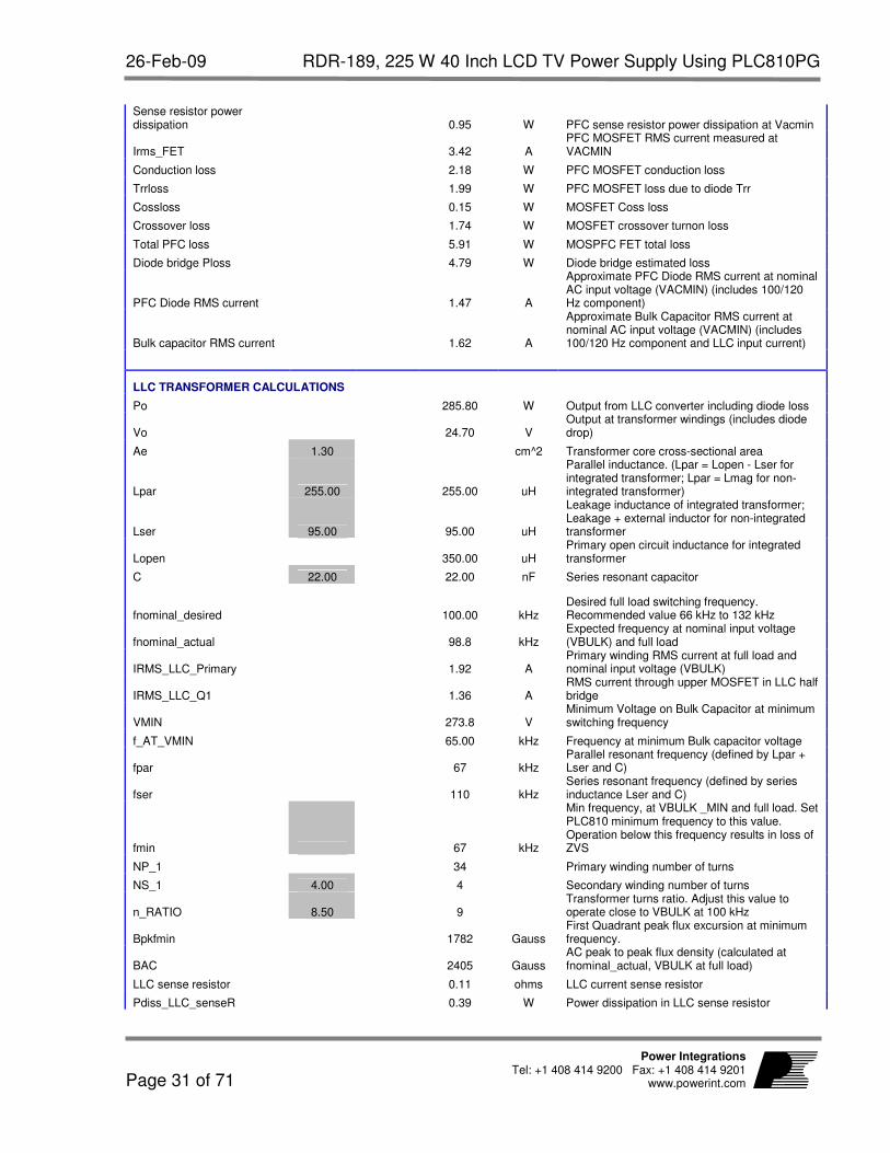
LLC TRANSFORMER CALCULATIONS
Po 285.80 W Output from LLC converter including diode loss
Vo 24.70 V Output at transformer windings (includes diode drop)
Ae 1.30 cm^2 Transformer core cross-sectional area
Lpar 255.00 255.00 uH
Parallel inductance. (Lpar = Lopen - Lser for integrated transformer; Lpar = Lmag for non-integrated transformer)
Lser 95.00 95.00 uH
Leakage inductance of integrated transformer; Leakage + external inductor for non-integrated transformer
Lopen 350.00 uH Primary open circuit inductance for integrated transformer
C 22.00 22.00 nF Series resonant capacitor
fnominal_desired 100.00 kHz Desired full load switching frequency. Recommended value 66 kHz to 132 kHz
fnominal_actual 98.8 kHz Expected frequency at nominal input voltage (VBULK) and full load
IRMS_LLC_Primary 1.92 A Primary winding RMS current at full load and nominal input voltage (VBULK)
IRMS_LLC_Q1 1.36 A RMS current through upper MOSFET in LLC half bridge
VMIN 273.8 V Minimum Voltage on Bulk Capacitor at minimum switching frequency
f_AT_VMIN 65.00 kHz Frequency at minimum Bulk capacitor voltage
fpar 67 kHz Parallel resonant frequency (defined by Lpar + Lser and C)
fser 110 kHz Series resonant frequency (defined by series inductance Lser and C)
fmin 67 kHz
Min frequency, at VBULK _MIN and full load. Set PLC810 minimum frequency to this value. Operation below this frequency results in loss of ZVS
NP_1 34 Primary winding number of turns
NS_1 4.00 4 Secondary winding number of turns
n_RATIO 8.50 9 Transformer turns ratio. Adjust this value to operate close to VBULK at 100 kHz
Bpkfmin 1782 Gauss First Quadrant peak flux excursion at minimum frequency.
BAC 2405 Gauss AC peak to peak flux density (calculated at fnominal_actual, VBULK at full load)
LLC sense resistor 0.11 ohms LLC current sense resistor
Pdiss_LLC_senseR 0.39 W Power dissipation in LLC sense resistor

RDR-189, 225 W 40 Inch LCD TV Power Supply Using PLC810PG 26-Feb-09
Page 32 of 71
Power Integrations Tel: +1 408 414 9200 Fax: +1 408 414 9201 www.powerint.com
PRIMARY
Primary gauge 38.00 AWG Individual wire strand gauge used for primary winding
Equivalent Primary Metric Wire gauge 0.10 mm Equivalent diameter of wire in metric units
Primary litz strands 70.00 Number of strands used in Litz wire; for non-litz non-integrated transformer set to 1
Primary parallel wires 1.00 Number of parallel individual wires to make up Litz wire
Resistivity_25 C_Primary 33.50 m-
ohm/m Resistivity in milli-ohms per meter
Transformer primary MLT 7.00 cm Mean length per turn
Primary turns 34.00 Number of primary turns
Primary DCR 25 C 79.74 m-ohm Estimated resistance at 25 C
Primary DCR 100 C 106.85 m-ohm Estimated resistance at 100 C (approximately 33% higher than at 25 C)
Primary RMS current 1.50 A Measured RMS current through the primary winding
ACR_Trf_Primary 170.96 m-ohm
Measured AC resistance (at 100 kHz, room temperature), multiply by 1.33 to approximate 100 C winding temperature
Primary copper loss 0.38 W Total primary winding copper loss at 85 C
Separate Series Inductor (For non-integrated transformer only)
Lsep 95.00 uH Desired inductance from separate inductor
Ae_Ind 0.53 cm^2 Inductor core cross-sectional area
Inductor turns 25.00 25 Number of primary turns
BP_fnom 2086 Gauss AC flux for core loss calculations (at fnom and full load)
BP_fmin 2575 Gauss Peak flux density, calculated at minimum frequency fmin
Inductor gauge 36.00 AWG Individual wire strand gauge used for primary winding
Equivalent Inductor Metric Wire gauge 0.13 mm Equivalent diameter of wire in metric units
Inductor litz strands 60.00 Number of strands used in Litz wire
Inductor parallel wires 1.00 Number of parallel individual wires to make up Litz wire
Resistivity_25 C_Sep_Ind 24.58 m-
ohm/m Resistivity in milli-ohms per meter
Inductor MLT 7.00 cm Mean length per turn
Inductor DCR 25 C 43.02 m-ohm Estimated resistance at 25 C (for reference)
Inductor DCR 100 C 57.65 m-ohm Estimated resistance at 100 C (approximately 33% higher than at 25 C)
ACR_Sep_Inductor 92.24 m-ohm
Measured AC resistance (at 100 kHz, room temperature), multiply by 1.33 to approximate 100 C winding temperature
Inductor copper loss 0.21 W Total primary winding copper loss at 85 C
Secondary 1 (Vo1) Note - Power loss calculations are for each winding half of secondary
Sec 1 Wire gauge 38 AWG Individual wire strand gauge used for secondary winding
Equivalent secondary 1 Metric Wire gauge 0.10 mm Equivalent diammeter of wire in metric units
Sec 1 litz strands 100 Number of strands used in Litz wire; for non-litz non-integrated transformer set to 1
Parallel wires sec 1 1 Number of parallel individual wires to make up

26-Feb-09 RDR-189, 225 W 40 Inch LCD TV Power Supply Using PLC810PG
Page 33 of 71
Power Integrations Tel: +1 408 414 9200 Fax: +1 408 414 9201
www.powerint.com
Litz wire
Resistivity_25 C_sec1 23.45 m-
ohm/m Resistivity in milli-ohms per meter Transformer Secondary MLT 7.00 cm Mean length per turn
Sec 1 Turns 4.00 Secondary winding turns (each half)
DCR_25C_Sec1 3.28 m-ohm Estimated resistance at 25 C (for reference)
DCR_100C_Sec1 4.40 m-ohm Estimated resistance at 100 C (approximately 33% higher than at 25 C)
Sec 1 RMS current 14.15 A RMS current through Output 1 winding, assuming half sinusoidal waveshape
DCR_Ploss_Sec1 0.71 W Estimated Power loss due to DC resistance (both secondary halves)
ACR_Sec1 7.04 m-ohm
Measured AC resistance (at 100 kHz, room temperature), multiply by 1.33 to approximate 100 C winding temperature . Default value of ACR is twice the DCR value at 100 C
ACR_Ploss_Sec1 2.82 W Estimated AC copper loss (both secondary halves)
Total secondary winding Copper Losses 2.82 W
Total (AC + DC) winding copper loss for both secondary halves
Secondary 2 (Vo2) Note - Power loss calculations are for each winding half of secondary
Sec 2 Wire gauge 38 AWG Individual wire strand gauge used for secondary winding
Equivalent secondary 2 Metric Wire gauge 0.10 mm Equivalent diammeter of wire in metric units
Sec 2 litz strands 100 Number of strands used in Litz wire; for non-litz non-integrated transformer set to 1
Parallel wires sec 2 2 Number of parallel individual wires to make up Litz wire
Resistivity_25 C_sec2 11.73 m-
ohm/m Resistivinty in milli-ohms per meter Transformer Secondary 2 MLT 7.00 cm Mean length per turn
Sec 2 Turns 2.00 Secondary winding turns (each half)
DCR_25C_Sec2 1.64 m-ohm Estimated resistance at 25 C (for reference)
DCR_100C_Sec2 2.20 m-ohm Estimated resistance at 100 C for half secondary (approximately 33% higher than at 25 C)
Sec 2 RMS current 22.01 Arms
RMS current through Output 2 winding; Output 1 winding is AC stacked on top of Output 2 winding
DCR_Ploss_Sec1 0.86 W Estimated Power loss due to DC resistance (both secondary halves)
ACR_Sec2 3.52 m-ohm
Actual measured AC resistance (at 100 kHz, room temperature), multiply by 1.33 to approximate 100 C winding temperature . Default value of ACR is twice the DCR value at 100 C
ACR_Ploss_Sec2 3.41 W Estimated AC copper loss (both secondary halves)
Total Copper loss calculation Does not include fringing flux loss from gap Primary copper loss (from Primary section) 0.38 W Total primary winding copper loss at 85 C
Secondary copper Loss 7.80 W Total copper loss in secondary winding
Transformer copper loss 8.19 W Total copper loss in transformer (primary + secondary)

RDR-189, 225 W 40 Inch LCD TV Power Supply Using PLC810PG 26-Feb-09
Page 34 of 71
Power Integrations Tel: +1 408 414 9200 Fax: +1 408 414 9201 www.powerint.com
TURNS CALCULATOR This is to help you choose the secondary turns - not connected to any other part of spreadsheet
V1 24.00 V Target Output Voltage Vo1
V1d1 0.70 V Diode drop voltage for Vo1
N1 4.00 Total number of turns for Vo1
V2 11.65 V Expected outputV
V2d2 0.70 V Diode drop voltage for Vo2
N2 2.00 Total number of turns for Vo2

26-Feb-09 RDR-189, 225 W 40 Inch LCD TV Power Supply Using PLC810PG
Page 35 of 71
Power Integrations Tel: +1 408 414 9200 Fax: +1 408 414 9201
www.powerint.com
Full load Primary and MOSFET RMS currents
0
1
2
3
4
5
30 60 90 120 150 180 210 240 270 300
Switching Frequency (kHz)
Irm
s (
A)
Primary
MOSFET
VBULK vs Switching Frequency
100
200
300
400
500
30 60 90 120 150
Switching Frequency (kHz)
VB
UL
K (
V)
Full load
Min load

RDR-189, 225 W 40 Inch LCD TV Power Supply Using PLC810PG 26-Feb-09
Page 36 of 71
Power Integrations Tel: +1 408 414 9200 Fax: +1 408 414 9201 www.powerint.com
9 RD-189 Performance Data
All measurements were taken at room temperature and 60 Hz input frequency unless otherwise specified, with 60 Hz input frequency. Voltage measurements were taken at the output connectors.
9.1 LLC Stage Efficiency
To make this measurement, capacitor C22 is shorted to allow the supply to operate with no AC input. The LLC stage was supplied by connecting an external HV DC supply across bulk capacitor C9. This supply was set to 385 VDC. The remote on switch was set to the “on” position.
80%
85%
90%
95%
0 50 100 150 200 250 300
Output Power (W)
Eff
icie
nc
y
5 V Unloaded
5 V Loadingscaled with main
385 VDC Input
Figure 15 – LLC Stage Efficiency vs. Load, 385 VDC Input.

26-Feb-09 RDR-189, 225 W 40 Inch LCD TV Power Supply Using PLC810PG
Page 37 of 71
Power Integrations Tel: +1 408 414 9200 Fax: +1 408 414 9201
www.powerint.com
9.2 Total Efficiency
Figures below show the total supply efficiency (PFC and LLC stages). AC input was supplied using a sine wave source.
70%
75%
80%
85%
90%
95%
80 120 160 200 240 280
AC Input Voltage (VAC)
Eff
icie
nc
y100% Load (233 W)
50% Load
20% Load
10% Load
Figure 16 – Total Efficiency vs. Output Power, 5 V Output Loaded.
70%
75%
80%
85%
90%
95%
80 120 160 200 240 280
AC Input Voltage (VAC)
Eff
icie
nc
y
100% Load (233 W)
50% Load
20% load
10% load
Figure 17 – Total Efficiency vs. Output Power, 5 V Output Unloaded.

RDR-189, 225 W 40 Inch LCD TV Power Supply Using PLC810PG 26-Feb-09
Page 38 of 71
Power Integrations Tel: +1 408 414 9200 Fax: +1 408 414 9201 www.powerint.com
9.3 +5 V Standby Output – Input Power vs Output Power
0.01
0.1
1
10
0.1 1 10
Input Power (W)
Ou
tpu
t P
ow
er
(W)
90 VAC
100 VAC
115 VAC
180 VAC
230 VAC
Figure 18 – Standby Input Power vs. Output Power.
The figure above shows standby input power as a function of output power, with the PFC and LLC stages disabled via the remote enable (remote-on switch set to “off” position).

26-Feb-09 RDR-189, 225 W 40 Inch LCD TV Power Supply Using PLC810PG
Page 39 of 71
Power Integrations Tel: +1 408 414 9200 Fax: +1 408 414 9201
www.powerint.com
9.4 Standby Load Raw Data
Table 1 shows the raw data taken from standby input power measurements. This is the same data as presented in Figure 18 but allows differentiation between operation at 90 VAC, 100 VAC and 115 VAC.
POUT vs PIN for Standby Supply
VIN (VAC) VO (V) IO (A) PIN (W) POUT (W)
90 5.07 0 0.045 0
90 5.07 0.0229 0.2 0.116
90 5.07 0.0714 0.5 0.362
90 5.07 0.154 0.9999 0.788
90 5.07 0.3208 2.004 1.626
100 5.07 0 0.0507 0
100 5.06 0.0229 0.199 0.116
100 5.07 0.0714 0.499 0.362
100 5.06 0.154 1.002 0.779
100 5.06 0.3208 2 1.623
115 5.07 0 0.0596 0
115 5.07 0.0209 0.2 0.106
115 5.07 0.069 0.5 0.350
115 5.06 0.1529 1.003 0.774
115 5.06 0.323 2.01 1.634
180 5.07 0 0.112 0
180 5.07 0.01299 0.2 0.066
180 5.07 0.0598 0.499 0.303
180 5.07 0.142 0.998 0.720
180 5.06 0.308 2 1.558
230 5.07 0 0.172 0
230 5.07 0.0053 0.205 0.027
230 5.07 0.0505 0.503 0.256
230 5.07 0.1318 1.002 0.668
230 5.07 0.2982 2.009 1.5119
Table 1 – Standby Input Power Raw Data.
RDR-189, 225 W 40 Inch LCD TV Power Supply Using PLC810PG 26-Feb-09
Page 40 of 71
Power Integrations Tel: +1 408 414 9200 Fax: +1 408 414 9201 www.powerint.com
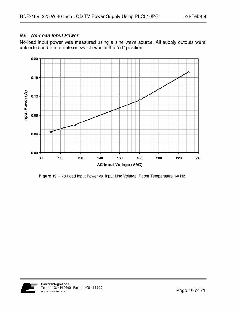
9.5 No-Load Input Power
No-load input power was measured using a sine wave source. All supply outputs were unloaded and the remote on switch was in the “off” position.
0.00
0.04
0.08
0.12
0.16
0.20
80 100 120 140 160 180 200 220 240
AC Input Voltage (VAC)
Inp
ut
Po
we
r (W
)
Figure 19 – No-Load Input Power vs. Input Line Voltage, Room Temperature, 60 Hz.
26-Feb-09 RDR-189, 225 W 40 Inch LCD TV Power Supply Using PLC810PG
Page 41 of 71
Power Integrations Tel: +1 408 414 9200 Fax: +1 408 414 9201
www.powerint.com
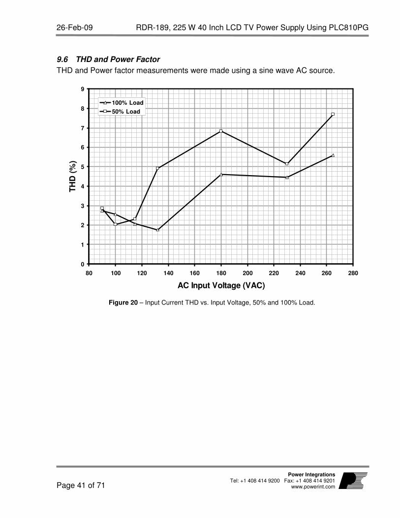
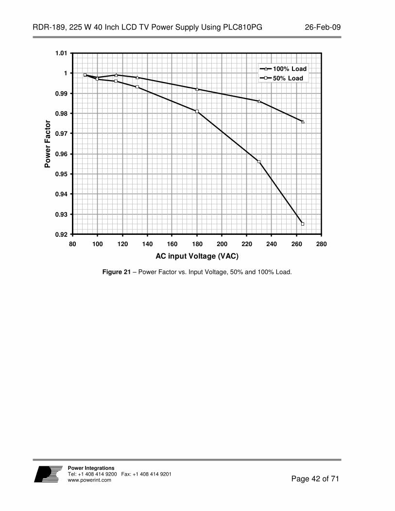
9.6 THD and Power Factor
THD and Power factor measurements were made using a sine wave AC source.
0
1
2
3
4
5
6
7
8
9
80 100 120 140 160 180 200 220 240 260 280
AC Input Voltage (VAC)
TH
D (
%)
100% Load
50% Load
Figure 20 – Input Current THD vs. Input Voltage, 50% and 100% Load.
RDR-189, 225 W 40 Inch LCD TV Power Supply Using PLC810PG 26-Feb-09
Page 42 of 71
Power Integrations Tel: +1 408 414 9200 Fax: +1 408 414 9201 www.powerint.com
0.92
0.93
0.94
0.95
0.96
0.97
0.98
0.99
1
1.01
80 100 120 140 160 180 200 220 240 260 280
AC input Voltage (VAC)
Po
we
r F
ac
tor
100% Load
50% Load
Figure 21 – Power Factor vs. Input Voltage, 50% and 100% Load.

26-Feb-09 RDR-189, 225 W 40 Inch LCD TV Power Supply Using PLC810PG
Page 43 of 71
Power Integrations Tel: +1 408 414 9200 Fax: +1 408 414 9201
www.powerint.com
9.7 Output Regulation
97%
98%
99%
100%
101%
102%
103%
104%
105%
0 10 20 30
Output Voltage (V)
Re
gu
lati
on
(%
)
5 V Output
12 V Output
24 V Output
Figure 22 – Output Regulation Across Load (10% to 100% loading).
The graph shows the output voltage variation of the outputs with load. The PFC regulates the LLC and standby supply input voltage under normal conditions so the outputs will not be affected by the AC input voltage. Variations due to temperature and component tolerances are not represented. The 12 V and 24 V outputs vary by less than 5%. The feedback circuit has equal weighting between the two outputs. If one output needs to be more tightly regulated then the other will suffer poorer regulation.
RDR-189, 225 W 40 Inch LCD TV Power Supply Using PLC810PG 26-Feb-09
Page 44 of 71
Power Integrations Tel: +1 408 414 9200 Fax: +1 408 414 9201 www.powerint.com
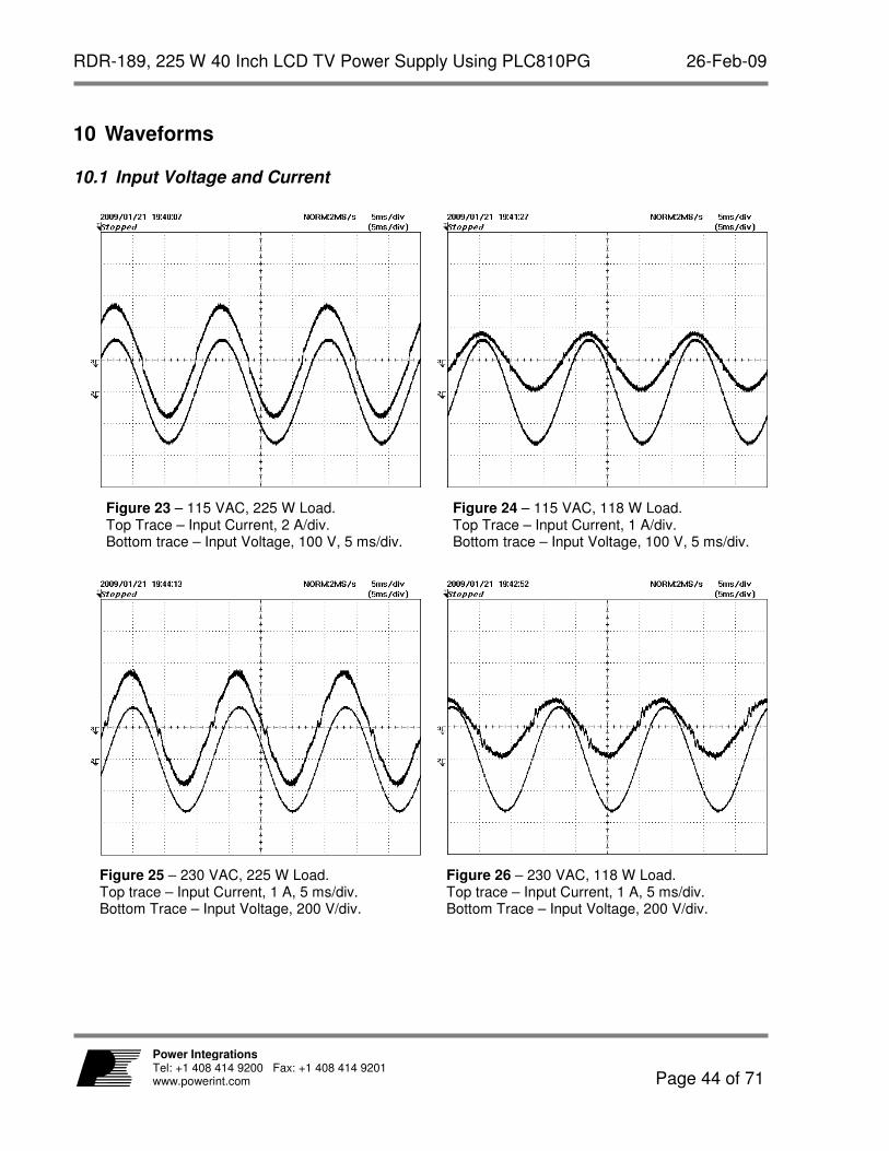
10 Waveforms
10.1 Input Voltage and Current
Figure 23 – 115 VAC, 225 W Load. Top Trace – Input Current, 2 A/div. Bottom trace – Input Voltage, 100 V, 5 ms/div.
Figure 24 – 115 VAC, 118 W Load. Top Trace – Input Current, 1 A/div. Bottom trace – Input Voltage, 100 V, 5 ms/div.
Figure 25 – 230 VAC, 225 W Load. Top trace – Input Current, 1 A, 5 ms/div. Bottom Trace – Input Voltage, 200 V/div.
Figure 26 – 230 VAC, 118 W Load. Top trace – Input Current, 1 A, 5 ms/div. Bottom Trace – Input Voltage, 200 V/div.

26-Feb-09 RDR-189, 225 W 40 Inch LCD TV Power Supply Using PLC810PG
Page 45 of 71
Power Integrations Tel: +1 408 414 9200 Fax: +1 408 414 9201
www.powerint.com
10.2 LLC Primary Voltage and Current
The LLC stage current was measured by replacing jumper JP26 with a current sensing loop that measures the LLC transformer (T3) primary current. The primary voltage waveform was measured at the hot side of ferrite bead inductor L6.
Figure 27 – LLC Stage Primary Voltage and Current.
Top Trace – Current, 2 A/div.
Bottom Trace – Voltage, 200 V, 2 µs/div.
RDR-189, 225 W 40 Inch LCD TV Power Supply Using PLC810PG 26-Feb-09
Page 46 of 71
Power Integrations Tel: +1 408 414 9200 Fax: +1 408 414 9201 www.powerint.com
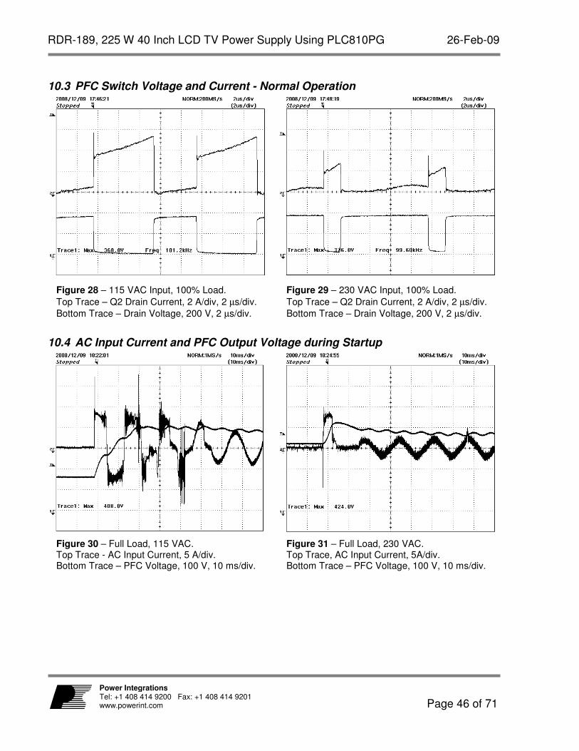
10.3 PFC Switch Voltage and Current - Normal Operation
Figure 28 – 115 VAC Input, 100% Load.
Top Trace – Q2 Drain Current, 2 A/div, 2 µs/div.
Bottom Trace – Drain Voltage, 200 V, 2 µs/div.
Figure 29 – 230 VAC Input, 100% Load.
Top Trace – Q2 Drain Current, 2 A/div, 2 µs/div.
Bottom Trace – Drain Voltage, 200 V, 2 µs/div.
10.4 AC Input Current and PFC Output Voltage during Startup
Figure 30 – Full Load, 115 VAC. Top Trace - AC Input Current, 5 A/div. Bottom Trace – PFC Voltage, 100 V, 10 ms/div.
Figure 31 – Full Load, 230 VAC. Top Trace, AC Input Current, 5A/div. Bottom Trace – PFC Voltage, 100 V, 10 ms/div.

26-Feb-09 RDR-189, 225 W 40 Inch LCD TV Power Supply Using PLC810PG
Page 47 of 71
Power Integrations Tel: +1 408 414 9200 Fax: +1 408 414 9201
www.powerint.com
10.5 LLC Startup
Figure 32 – LLC Startup. 115 VAC, 100% Load, Using Remote Start. Top Trace – LLC Primary Current, 5 A/div. Bottom Trace – Q11 Drain Voltage, 200 V, 10 ms/div.

RDR-189, 225 W 40 Inch LCD TV Power Supply Using PLC810PG 26-Feb-09
Page 48 of 71
Power Integrations Tel: +1 408 414 9200 Fax: +1 408 414 9201 www.powerint.com
10.6 LLC Output Short Circuit
The figure below shows the effect of a 24 V output short circuit on the LLC primary current. A mercury displacement relay was used to short the 24 V output to get a fast, bounce-free connection.
Figure 33 – Output Short Circuit Test (24 V). Top Trace – LLC Primary Current, 5 A/div.
Bottom Trace – 24 V Output, 5 V, 50 µs/div.

26-Feb-09 RDR-189, 225 W 40 Inch LCD TV Power Supply Using PLC810PG
Page 49 of 71
Power Integrations Tel: +1 408 414 9200 Fax: +1 408 414 9201
www.powerint.com
10.7 Output Voltage during Startup and Shutdown
10.7.1 Standby Supply
Figure 34 – 5 V Standby Output at Start-up. 115 VAC Input. No Load. 1 V, 10 ms/div.
Figure 35 – 5 V Standby Output at Start-up. 115 VAC Input. 100 mA Load. 1 V, 10 ms/div.
Figure 36 – 5 V Standby Output at Start-up. 230 VAC Input. No Load. 1 V, 10 ms/div.
Figure 37 – 5 V Standby Output at Start-up. 230 VAC Input. 100 mA Load. 1 V, 10 ms/div.
RDR-189, 225 W 40 Inch LCD TV Power Supply Using PLC810PG 26-Feb-09
Page 50 of 71
Power Integrations Tel: +1 408 414 9200 Fax: +1 408 414 9201 www.powerint.com
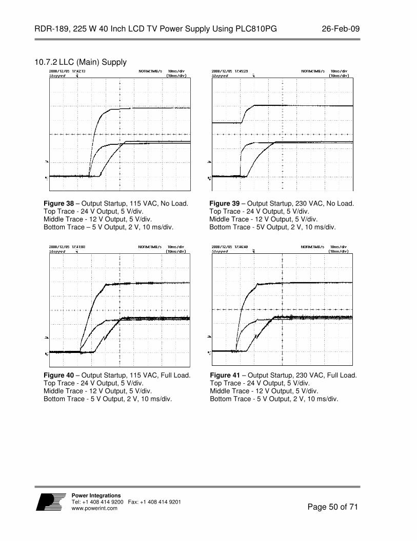
10.7.2 LLC (Main) Supply
Figure 38 – Output Startup, 115 VAC, No Load. Top Trace - 24 V Output, 5 V/div. Middle Trace - 12 V Output, 5 V/div. Bottom Trace – 5 V Output, 2 V, 10 ms/div.
Figure 39 – Output Startup, 230 VAC, No Load. Top Trace - 24 V Output, 5 V/div. Middle Trace - 12 V Output, 5 V/div. Bottom Trace - 5V Output, 2 V, 10 ms/div.
Figure 40 – Output Startup, 115 VAC, Full Load. Top Trace - 24 V Output, 5 V/div. Middle Trace - 12 V Output, 5 V/div. Bottom Trace - 5 V Output, 2 V, 10 ms/div.
Figure 41 – Output Startup, 230 VAC, Full Load. Top Trace - 24 V Output, 5 V/div. Middle Trace - 12 V Output, 5 V/div. Bottom Trace - 5 V Output, 2 V, 10 ms/div.
26-Feb-09 RDR-189, 225 W 40 Inch LCD TV Power Supply Using PLC810PG
Page 51 of 71
Power Integrations Tel: +1 408 414 9200 Fax: +1 408 414 9201
www.powerint.com
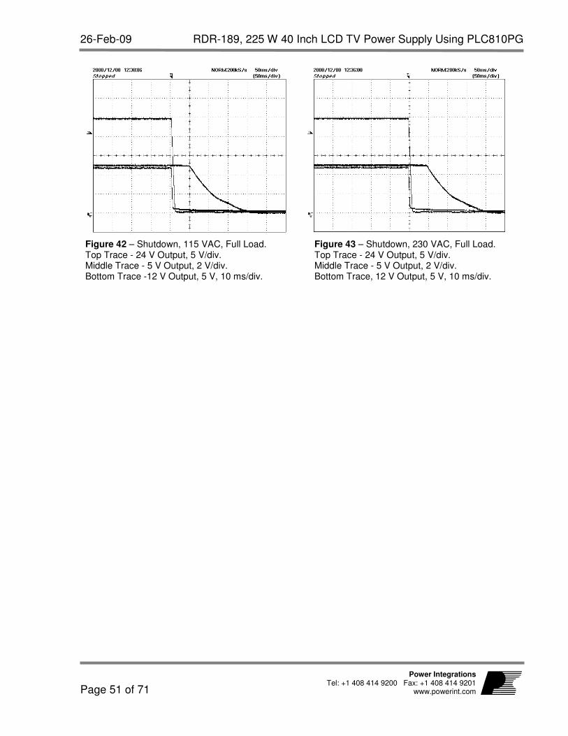
Figure 42 – Shutdown, 115 VAC, Full Load. Top Trace - 24 V Output, 5 V/div. Middle Trace - 5 V Output, 2 V/div. Bottom Trace -12 V Output, 5 V, 10 ms/div.
Figure 43 – Shutdown, 230 VAC, Full Load. Top Trace - 24 V Output, 5 V/div. Middle Trace - 5 V Output, 2 V/div. Bottom Trace, 12 V Output, 5 V, 10 ms/div.
RDR-189, 225 W 40 Inch LCD TV Power Supply Using PLC810PG 26-Feb-09
Page 52 of 71
Power Integrations Tel: +1 408 414 9200 Fax: +1 408 414 9201 www.powerint.com
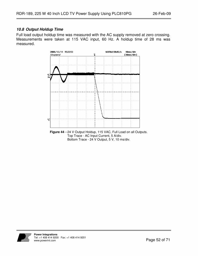
10.8 Output Holdup Time
Full load output holdup time was measured with the AC supply removed at zero crossing. Measurements were taken at 115 VAC input, 60 Hz. A holdup time of 28 ms was measured.
Figure 44 – 24 V Output Holdup, 115 VAC, Full Load on all Outputs. Top Trace - AC Input Current, 5 A/div. Bottom Trace - 24 V Output, 5 V, 10 ms/div.
26-Feb-09 RDR-189, 225 W 40 Inch LCD TV Power Supply Using PLC810PG
Page 53 of 71
Power Integrations Tel: +1 408 414 9200 Fax: +1 408 414 9201
www.powerint.com
10.9 Output Ripple Measurements
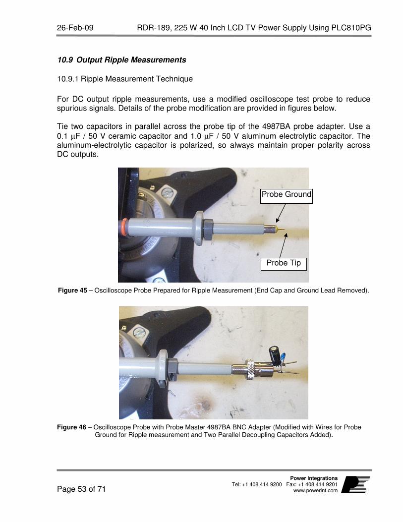
10.9.1 Ripple Measurement Technique
For DC output ripple measurements, use a modified oscilloscope test probe to reduce spurious signals. Details of the probe modification are provided in figures below. Tie two capacitors in parallel across the probe tip of the 4987BA probe adapter. Use a
0.1 µF / 50 V ceramic capacitor and 1.0 µF / 50 V aluminum electrolytic capacitor. The aluminum-electrolytic capacitor is polarized, so always maintain proper polarity across DC outputs.
Figure 45 – Oscilloscope Probe Prepared for Ripple Measurement (End Cap and Ground Lead Removed).
Figure 46 – Oscilloscope Probe with Probe Master 4987BA BNC Adapter (Modified with Wires for Probe Ground for Ripple measurement and Two Parallel Decoupling Capacitors Added).
Probe Ground
Probe Tip

RDR-189, 225 W 40 Inch LCD TV Power Supply Using PLC810PG 26-Feb-09
Page 54 of 71
Power Integrations Tel: +1 408 414 9200 Fax: +1 408 414 9201 www.powerint.com
10.9.2 Full Load Output Ripple Results
Figure 47 – 5 V Output Ripple, 50 mV, 50 µs/div. Figure 48 – 12 V Output Ripple, 50 mV, 5 ms/div.
Figure 49 – 12 V Output Ripple, 50 mV, 2 µs/div. Figure 50 – 24 V Output Ripple, 50 mV, 2 µs/div.

26-Feb-09 RDR-189, 225 W 40 Inch LCD TV Power Supply Using PLC810PG
Page 55 of 71
Power Integrations Tel: +1 408 414 9200 Fax: +1 408 414 9201
www.powerint.com
10.9.3 Output Load Step Response
The figures below show transient response with a 75%-100%-75% load step for both the 5 V and the 24 V output.
Figure 51 – 5 V Output Transient Response 1.5 A – 2A – 1.5A Load Step. 5 V Standby Output Unloaded, +12 V, +24 V Outputs Full Load. Top Trace – 5 V Transient Response, 50 mV/div.
Bottom Trace – 5 V Load Step, 1 A, 500 µs/div.
Figure 52 – 12 V / 24 V Output Transient Response 6.75 A – 9 A – 6.75 A Load Step on 24 V. 5 V, 12 V, Outputs Full Load. Top Trace – 24 V Transient Response, 200 mV/div. Middle Trace – +12 V Transient Response, 100 mV/div.
Bottom Trace – 24 V Load Step, 5 A, 500 µs/div.

RDR-189, 225 W 40 Inch LCD TV Power Supply Using PLC810PG 26-Feb-09
Page 56 of 71
Power Integrations Tel: +1 408 414 9200 Fax: +1 408 414 9201 www.powerint.com
11 Temperature Profiles
The board was operated at room temperature in a vertical orientation as show below. Tape was placed on top of the two main heatsinks to correct emissivity and allow accurate temperature measurements when using an infra red (IR) camera. For each test condition the unit was allowed to thermally stabilize (>1 hr) before measurement were made. Infra red measurements were correlated to thermocouples attached using thermally conductive adhesive (Artic Silver).
Figure 53 – Photograph of Board Orientation Used for Thermal Testing.
LLC rectifier heatsink
PFC and input rectifier heatsink
LLC MOSFET heatsinks
PFC inductor
LLC transformer
Input bridge
PFC boost MOSFET
PFC boost diode
12 V 24 V output rectifiers

26-Feb-09 RDR-189, 225 W 40 Inch LCD TV Power Supply Using PLC810PG
Page 57 of 71
Power Integrations Tel: +1 408 414 9200 Fax: +1 408 414 9201
www.powerint.com
11.1 Thermal Results Summary
11.1.1 Testing Conditions
Testing was performed under conditions commonly specified by LCD TV manufacturers. The goal of the design is to maintain the temperature of components below 100 C at rated ambient and 80% load (184 W), low line (108 VAC, 57 Hz). In addition no component shall exceed the manufacturers limit under conditions of full load (225 W) and abnormal low line condition (90 VAC, 47 Hz). In both cases this design meets these requirements with extrapolated maximum
temperatures of 99°C for the PFC choke and 94°C for the LLC transformer secondary winding. Should a lower PFC choke temperature be desired then an alternate design is presented below. Measurement data is presented below. The unit was allowed to thermally stabilize (> 1 hours in all cases) before gathering data. Semiconductor plastic and heatsink temperatures were correlated via thermocouples attached with adhesive.
For the LLC transformer the secondary winding was 10-15°C hotter than the primary. For
the LLC rectifiers D9 (24 V output) was 10°C hotter than D10 (12 V output). Therefore only D9 and the secondary winding temperatures are shown below.
108 VAC, 57 Hz 108 VAC, 57 Hz 90 VAC, 47 Hz
Output Power (W) 230.1 184.1 230.1
Input Power (W) 264.7 211.1 268.3
Efficiency (%) 86.9% 87.2% 85.8%
Output Loading 12 V 4 A (11.83 V) 3.2 A (11.86 V) 4 A (11.83 V)
Output Loading 24 V 7 A (24.68V) 5.6 A (24.66 V) 7 A (24.69 V)
Output Loading 5 V 2 A (5.02 V) 1.6 A (5.03V) 2 A (5.02 V)
Temperatures (°°°°C)
Ambient 25 25 25
LLC rectifier heatsink 67 60 67
LLC rectifier plastic package (D9) 82 69 80
LLC MOSFET heatsink (Q10/Q11) 64 55 64
LLC MOSFET plastic package 67 57 66
PFC and rectifier Heatsink 71 63 76
PFC diode plastic package (D2) 76 68 84
PFC MOSFET plastic package (Q2) 82 72 91
Bridge rectifier plastic package (BR1) 80 70 87
LLC transformer (T2) surface (secondary)
91 79 90
PFC inductor (L4) winding surface 94 84 97

RDR-189, 225 W 40 Inch LCD TV Power Supply Using PLC810PG 26-Feb-09
Page 58 of 71
Power Integrations Tel: +1 408 414 9200 Fax: +1 408 414 9201 www.powerint.com
11.2 90 VAC, 47 Hz, 225 WOUT
Figure 54 – Thermal Profile. Room Temperature, 90 VAC, 47 Hz, 225 W Load (1 hr).
11.3 108 VAC, 57 Hz, 225 WOUT
Figure 55 – Thermal Profile. Room Temperature, 108 VAC, 57 Hz, 225 W Load (1 hr).

26-Feb-09 RDR-189, 225 W 40 Inch LCD TV Power Supply Using PLC810PG
Page 59 of 71
Power Integrations Tel: +1 408 414 9200 Fax: +1 408 414 9201
www.powerint.com
11.4 108 VAC, 57 Hz, 185 WOUT
Figure 56 – Thermal Profile. Room Temperature, 108 VAC, 57 Hz, 185 W Load (1 hr).

RDR-189, 225 W 40 Inch LCD TV Power Supply Using PLC810PG 26-Feb-09
Page 60 of 71
Power Integrations Tel: +1 408 414 9200 Fax: +1 408 414 9201 www.powerint.com
11.5 Alternate PFC Choke Designs for Lower Operating Temperature
The two PFC choke designs provide a lower choke operating temperature.
Choke Type Choke Temperature
90 VAC, 286 W Output, 25°C Original EE35 115 °C
EE41 72 °C
34 mm Toroid 81 °C
11.5.1 34 mm Toroidal Choke
11.5.1.1 Electrical Diagram
Figure 57 – Electrical Diagram, Toroidal PFC Inductor
11.5.1.2 Electrical Specification
Inductance: 576 µH ± 15%
11.5.1.3 Materials
Item Description [1] Toroid: Sendust, 60µ 34 mm OD x 19 mm ID x 12 mm HT, Chang Sung CS330060
or equivalent. [2] Magnet Wire: #18AWG, solderable double coated. [3] Tape Polyester Film, 3M 1350F-1, or equivalent, 19.5mm wide. [4] Tape, Copper Foil, 3M 1125, or equivalent, 14mm wide. [5] Wire, hook-up, 22AWG UL1015, black. [6] Tie wrap Nylon 99mm Panduit PLT-IM or equivalent

26-Feb-09 RDR-189, 225 W 40 Inch LCD TV Power Supply Using PLC810PG
Page 61 of 71
Power Integrations Tel: +1 408 414 9200 Fax: +1 408 414 9201
www.powerint.com
11.5.1.4 Build Diagram
Figure 58 – Build Diagram, Toroidal PFC Inductor.
11.5.1.5 Winding Instructions
1 Apply tie wrap (item [6]) to core as shown in build diagram 2 Wind 47 turns of wire (item [2]) to form one complete layer. 3 Reverse the winding direction and apply 36 turns on top of previous layer to form complete
second layer. 4 Reverse winding direction, apply 13 turns on top of second layer to form ~1/4 third layer. 5 Apply 3 turns of tape (item [3]) around core circumference. 6 Apply 1 turn of copper tape (item [4]) around circumference of core with ends overlapping 2-3
mm. Solder end of tape to form shorted turn. 7 Take 7cm of hook-up wire (item[5]) , strip ends 1 cm, solder 1 end of wire to copper foil as shown
in build diagram, approximately 90 degrees clockwise around core circumference from start and finish leads.
8 Apply 2 turns of tape (item [3]) around the core circumference. 9 Trim start and finish leads to 5 cm, solder tin ends 1 cm. (Figure1). Finished inductor should
appear as shown in build diagram
Tin 1cm (2places)
5cm
Tie wrap Item[6]
Item [5]
Item [3]Item [4]Solder (1 place)

RDR-189, 225 W 40 Inch LCD TV Power Supply Using PLC810PG 26-Feb-09
Page 62 of 71
Power Integrations Tel: +1 408 414 9200 Fax: +1 408 414 9201 www.powerint.com
11.5.1.6 Temperature Measurement for Toroidal Inductor
Figure 59 – Temperature Measurement for Toroidal PFC Inductor 90 VAC input, Room Temperature, 286 W Output Power.

26-Feb-09 RDR-189, 225 W 40 Inch LCD TV Power Supply Using PLC810PG
Page 63 of 71
Power Integrations Tel: +1 408 414 9200 Fax: +1 408 414 9201
www.powerint.com
11.5.2 PFC Choke Using EE41/33 Core
11.5.2.1 Electrical Diagram, EE 41/33 PFC Choke
Figure 60 – Electrical Diagram, EE 41/33 PFC Choke.
11.5.2.2 Electrical Specification
Inductance: 576 µH ± 15%
Note – Do not measure inductance without copper strap in place
11.5.2.3 Materials
Item Description [1] E Core Pair: Sendust, 60 µ, EE41/33 Chang Sung S060 EE41/33 or equivalent. [2] Bobbin, E21, Horizontal, 12 pin, Ferroxcube CPH-E41/12-1S-12PD-Z or equivalent [3] Magnet Wire: #24AWG, solderable double coated. [4] Tape Polyester Film, 3M 1350F-1 or equivalent, 19 mm wide. [5] Tape Polyester Film, 3M 1350F-1 or equivalent, 10 mm wide. [6] Tape, Copper Foil, 3M 1125 or equivalent, 17 mm wide. [7] Wire, tinned bus, 24AWG. [8] Transformer Varnish, Dolph BC-389 or equivalent (must be baking vs. air-dry varnish)

RDR-189, 225 W 40 Inch LCD TV Power Supply Using PLC810PG 26-Feb-09
Page 64 of 71
Power Integrations Tel: +1 408 414 9200 Fax: +1 408 414 9201 www.powerint.com
11.5.2.4 Build Diagram
Figure 61 – EE41/33 PFC Choke Build Diagram.
Core [1]
Bus Wire [7]
Solder wire [7] here
Copper Tape [6]
Pin 1
Copper Tape [6]
Overlap ends and solder here
INCORRECT CORRECT Copper foil tape and insulating tape wrap must closely conform to core and winding
Copper tape [6] Polyester Tape [4]

26-Feb-09 RDR-189, 225 W 40 Inch LCD TV Power Supply Using PLC810PG
Page 65 of 71
Power Integrations Tel: +1 408 414 9200 Fax: +1 408 414 9201
www.powerint.com
11.5.2.5 Winding Instructions
1 Starting on Pin 1, wind 55 quadrifilar turns of wire (item [3]) on bobbin (Item [2]). Finish on Pin 6. 2 Use 3 layers of tape (Item [4]) for finish wrap. 3 Assemble bobbin and core halves. Secure core with two wraps of tape (Item 5). 4 Apply 1 turn of copper tape (Item [6]) as shown in Figure 1, centered in bobbin window. Closely
conform copper tape to contours of core and winding (see Figure 3). This step is essential for reducing operating noise. Overlap start and finish ends as shown in Figure 1, and solder to form a shorted turn. Take 3cm of hook-up wire (item[7]), solder 1 end of wire to copper foil as shown in Figure 1. Terminate other end on Pin 12 of bobbin .
5 Apply 3 turns of tape (item [4]) to insulate copper strap. Closely conform tape wrap to contours of core and winding (see build diagram).
6 Vacuum impregnate and bake finished assembly, cut off pins 7-8
11.5.2.6 Temperature Measurement
Figure 62 – Temperature Measurement for EE 41/33 PFC Choke Room Temperature, 90 VAC, 286 W Output Load.

RDR-189, 225 W 40 Inch LCD TV Power Supply Using PLC810PG 26-Feb-09
Page 66 of 71
Power Integrations Tel: +1 408 414 9200 Fax: +1 408 414 9201 www.powerint.com
12 LLC Gain-Phase
Figure 63 – LLC Converter Gain-Phase, 100% Load Crossover Frequency – 2 kHz, Phase Margin - 45°.
Figure 64 – LLC Converter Gain-Phase, 50% Load. Crossover Frequency ~1.8 kHz, Phase Margin - ~55°.
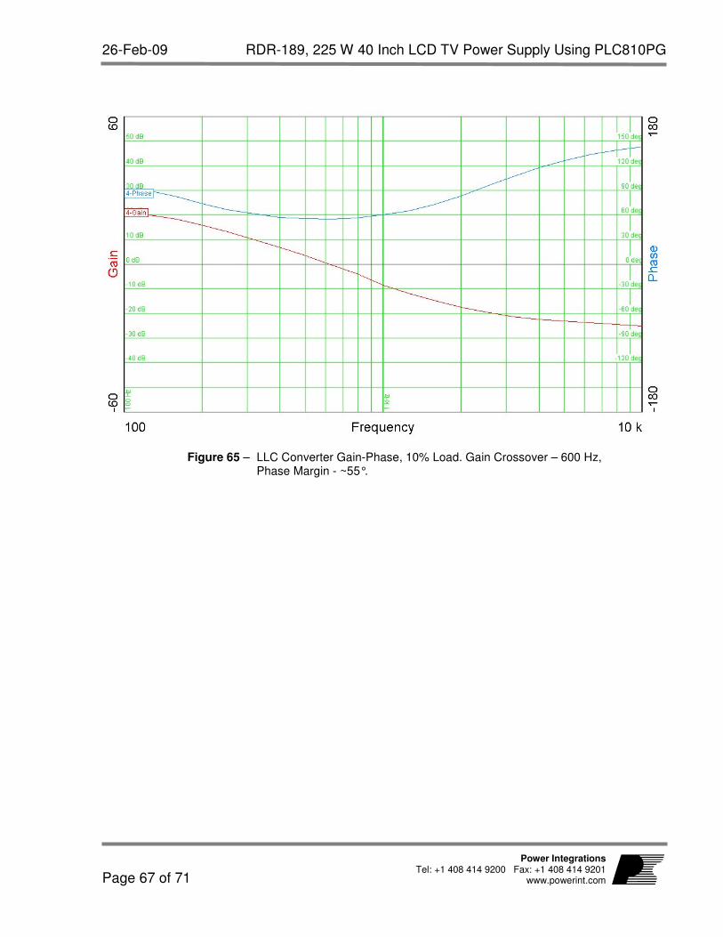
26-Feb-09 RDR-189, 225 W 40 Inch LCD TV Power Supply Using PLC810PG
Page 67 of 71
Power Integrations Tel: +1 408 414 9200 Fax: +1 408 414 9201
www.powerint.com
Figure 65 – LLC Converter Gain-Phase, 10% Load. Gain Crossover – 600 Hz, Phase Margin - ~55°.

RDR-189, 225 W 40 Inch LCD TV Power Supply Using PLC810PG 26-Feb-09
Page 68 of 71
Power Integrations Tel: +1 408 414 9200 Fax: +1 408 414 9201 www.powerint.com
13 Conducted EMI
Conducted EMI tests were performed with 3Ω resistive loads on the 12 V and 24 V main outputs, and a 2.5 Ω resistive load on the switched +5 V output (250 W total output power). The board was bolted to a metallic ground plane, which in turn was hard wired to LISN (protective earth) ground.
Figure 66 – Conducted EMI. 115 VAC.
Figure 67 – Conducted EMI, 230 VAC.
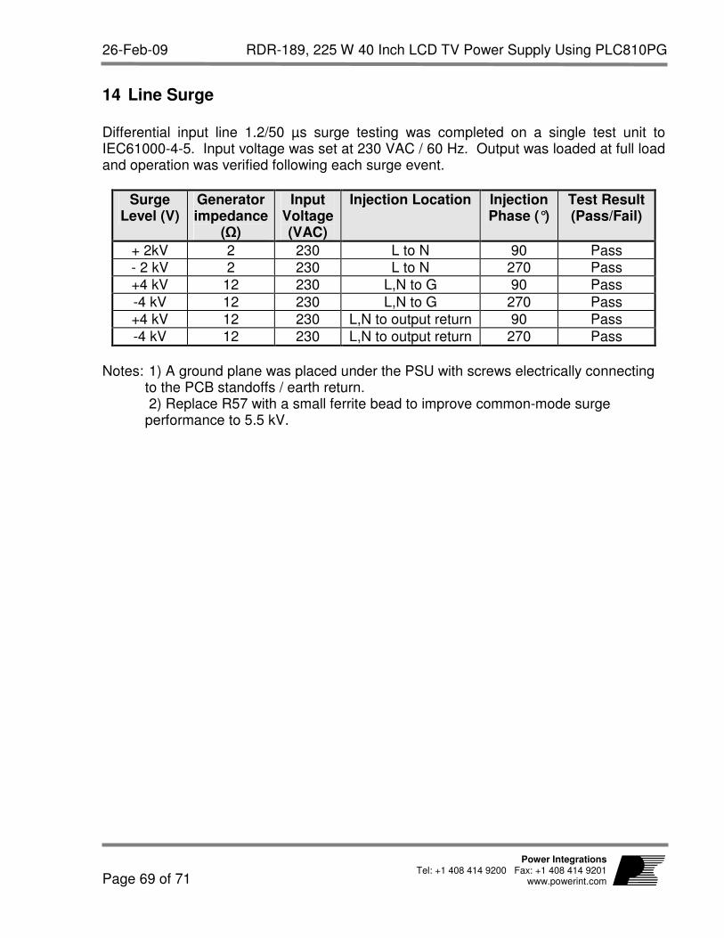
26-Feb-09 RDR-189, 225 W 40 Inch LCD TV Power Supply Using PLC810PG
Page 69 of 71
Power Integrations Tel: +1 408 414 9200 Fax: +1 408 414 9201
www.powerint.com
14 Line Surge
Differential input line 1.2/50 µs surge testing was completed on a single test unit to IEC61000-4-5. Input voltage was set at 230 VAC / 60 Hz. Output was loaded at full load and operation was verified following each surge event.
Surge Level (V)
Generator impedance
(Ω)
Input Voltage (VAC)
Injection Location Injection Phase (°)
Test Result (Pass/Fail)
+ 2kV 2 230 L to N 90 Pass - 2 kV 2 230 L to N 270 Pass
+4 kV 12 230 L,N to G 90 Pass
-4 kV 12 230 L,N to G 270 Pass
+4 kV 12 230 L,N to output return 90 Pass
-4 kV 12 230 L,N to output return 270 Pass
Notes: 1) A ground plane was placed under the PSU with screws electrically connecting
to the PCB standoffs / earth return. 2) Replace R57 with a small ferrite bead to improve common-mode surge
performance to 5.5 kV.

RDR-189, 225 W 40 Inch LCD TV Power Supply Using PLC810PG 26-Feb-09
Page 70 of 71
Power Integrations Tel: +1 408 414 9200 Fax: +1 408 414 9201 www.powerint.com
15 Revision History
Date Author Revision Description and changes Reviewed
29-Jan-09 PV 1.0.1 Initial Release MKTG, Apps 26-Feb-09 JC 1.0.2 Updated Surge Table, Minor Format
Updates MKTG, Apps

26-Feb-09 RDR-189, 225 W 40 Inch LCD TV Power Supply Using PLC810PG
Page 71 of 71
Power Integrations Tel: +1 408 414 9200 Fax: +1 408 414 9201
www.powerint.com
For the latest updates, visit our website: www.powerint.com
Power Integrations reserves the right to make changes to its products at any time to improve reliability or
manufacturability. Power Integrations does not assume any liability arising from the use of any device or circuit
described herein. POWER INTEGRATIONS MAKES NO WARRANTY HEREIN AND SPECIFICALLY DISCLAIMS ALL
WARRANTIES INCLUDING, WITHOUT LIMITATION, THE IMPLIED WARRANTIES OF MERCHANTABILITY,
FITNESS FOR A PARTICULAR PURPOSE, AND NON-INFRINGEMENT OF THIRD PARTY RIGHTS.
PATENT INFORMATION
The products and applications illustrated herein (including transformer construction and circuits external to the products)
may be covered by one or more U.S. and foreign patents, or potentially by pending U.S. and foreign patent applications
assigned to Power Integrations. A complete list of Power Integrations’ patents may be found at www.powerint.com.
Power Integrations grants its customers a license under certain patent rights as set forth at
http://www.powerint.com/ip.htm.
The PI Logo, TOPSwitch, TinySwitch, LinkSwitch, DPA-Switch, PeakSwitch, EcoSmart, Clampless, E-Shield, Filterfuse, StackFET,
PI Expert and PI FACTS are trademarks of Power Integrations, Inc. Other trademarks are property of their respective
companies. ©Copyright 2008 Power Integrations, Inc.
Power Integrations Worldwide Sales Support Locations
WORLD HEADQUARTERS 5245 Hellyer Avenue San Jose, CA 95138, USA. Main: +1-408-414-9200 Customer Service: Phone: +1-408-414-9665 Fax: +1-408-414-9765 e-mail: [email protected]
GERMANY Rueckertstrasse 3 D-80336, Munich Germany Phone: +49-89-5527-3911 Fax: +49-89-5527-3920 e-mail: [email protected]
JAPAN Kosei Dai-3 Bldg., 2-12-11, Shin-Yokohama, Kohoku-ku, Yokohama-shi, Kanagawa 222-0033 Phone: +81-45-471-1021 Fax: +81-45-471-3717 e-mail: [email protected]
TAIWAN 5F, No. 318, Nei Hu Rd., Sec. 1 Nei Hu Dist. Taipei, Taiwan 114, R.O.C. Phone: +886-2-2659-4570 Fax: +886-2-2659-4550 e-mail: [email protected]
CHINA (SHANGHAI) Rm 1601/1610, Tower 1, Kerry Everbright City No. 218 Tianmu Road West, Shanghai, P.R.C. 200070 Phone: +86-21-6354-6323 Fax: +86-21-6354-6325 e-mail: [email protected]
INDIA #1, 14
th Main Road
Vasanthanagar Bangalore-560052 India Phone: +91-80-41138020 Fax: +91-80-41138023 e-mail: [email protected]
KOREA RM 602, 6FL Korea City Air Terminal B/D, 159-6 Samsung-Dong, Kangnam-Gu, Seoul, 135-728, Korea Phone: +82-2-2016-6610 Fax: +82-2-2016-6630 e-mail: [email protected]
UNITED KINGDOM 1st Floor, St. James’s House East Street, Farnham Surrey, GU9 7TJ United Kingdom Phone: +44 (0) 1252-730-141 Fax: +44 (0) 1252-727-689 e-mail: [email protected]
CHINA (SHENZHEN) Rm A, B & C 4
th Floor, Block C,
Electronics Science and Technology Building, 2070 Shennan Zhong Rd, Shenzhen, Guangdong, China, 518031 Phone: +86-755-8379-3243 Fax: +86-755-8379-5828 e-mail: [email protected]
ITALY Via De Amicis 2 20091 Bresso MI – Italy Phone: +39-028-928-6000 Fax: +39-028-928-6009 e-mail: [email protected]
SINGAPORE 51 Newton Road, #15-08/10 Goldhill Plaza, Singapore, 308900 Phone: +65-6358-2160 Fax: +65-6358-2015 e-mail: [email protected]
APPLICATIONS HOTLINE World Wide +1-408-414-9660 APPLICATIONS FAX World Wide +1-408-414-9760