Nano-Electromechanical Optoelectronic Tunable … Optoelectronic Tunable Lasers by ......
176
Nano-Electromechanical Optoelectronic Tunable Lasers Michael Chung-Yi Huang Electrical Engineering and Computer Sciences University of California at Berkeley Technical Report No. UCB/EECS-2008-2 http://www.eecs.berkeley.edu/Pubs/TechRpts/2008/EECS-2008-2.html January 7, 2008
Transcript of Nano-Electromechanical Optoelectronic Tunable … Optoelectronic Tunable Lasers by ......
Nano-Electromechanical Optoelectronic TunableLasers
Michael Chung-Yi Huang
Electrical Engineering and Computer SciencesUniversity of California at Berkeley
Technical Report No. UCB/EECS-2008-2
http://www.eecs.berkeley.edu/Pubs/TechRpts/2008/EECS-2008-2.html
January 7, 2008

Copyright © 2008, by the author(s).All rights reserved.
Permission to make digital or hard copies of all or part of this work forpersonal or classroom use is granted without fee provided that copies arenot made or distributed for profit or commercial advantage and that copiesbear this notice and the full citation on the first page. To copy otherwise, torepublish, to post on servers or to redistribute to lists, requires prior specificpermission.
Acknowledgement
I would foremost like to thank my advisor, Professor Connie Chang-Hasnain, for her consummate intellect in academic and philosophicalmatters. Her knowledge, experience, dedication, vision and mostimportantly passion have stimulated my enthusiasm for pushing theforefront of research. Furthermore, her patience and faith in my abilitieshave inspired me on countless occasions. Without her guidance andmentorship, this work would not have come to fruition. In addition, I wouldlike to thank Prof. Ming Wu, Prof. Albert Pisano, and Prof. Yuri Suzuki fortheir useful comments and advices while serving on my qualify exam anddissertation committee.
Nano-Electromechanical Optoelectronic Tunable Lasers
by
Michael Chung-Yi Huang
B.S. (University of California, Berkeley) 2002
A dissertation submitted in partial satisfaction of the
requirements for the degree of
Doctor of Philosophy
in
Engineering – Electrical Engineering and Computer Sciences
And the Designated Emphasis
in
Nanoscale Science and Engineering
in the
Graduate Division
of the
UNIVERSITY of CALIFORNIA, BERKELEY
Committee in charge:
Professor Constance J. Chang-Hasnain, Cha ir Professor Ming C. Wu Professor Yuri Suzuki
Fall 2007
The dissertation of Michael Chung-Yi Huang is approved: _____________________________________________ __________________ Professor Constance J. Chang-Hasnain, Chair Date _____________________________________________ __________________ Professor Ming C. Wu Date _____________________________________________ __________________ Professor Yuri Suzuki Date
University of California, Berkeley
Fall 2007

Nano-Electromechanical Optoelectronic Tunable Lasers
© 2007
by Michael Chung-Yi Huang
1
ABSTRACT
Nano-Electromechanical Optoelectronic Tunable Lasers
by
Michael Chung-Yi Huang
Doctor of Philosophy in Engineering – Electrical Engineering and Computer Sciences
And the Designated Emphasis in Nanoscale Science and Engineering
University of California, Berkeley
Professor Connie J. Chang-Hasnain, Chair
Semiconductor diode lasers can be used in a variety of applications including
telecommunications, displays, optical data storage, solid-state lighting, sensing and
printing. Among them, vertical-cavity surface-emitting lasers (VCSELs) are particularly
promising. Because they emit light normal to the constituent wafer surface, it is possible
to extract light more efficiently and to fabricate two-dimensional device arrays. A
VCSEL contains two distributed Bragg reflector (DBR) mirrors for optical feedback,
separated by a very short active gain region. Typically, the reflectivity of the DBRs must
exceed 99.5% in order for the VCSEL to reach lasing operation. However, the realization
of practical VCSELs that can be used over a wide range of wavelengths has been
hindered by the poor optical and thermal properties of candidate DBR materials.
In this dissertation, we present a novel design of surface emitting lasers utilizing a
revolutionary, single- layer, high- index-contrast subwavelength grating (HCG), instead of
conventional a distributed Bragg reflector (DBRs). The HCG provides both efficient
optical feedback and control over the wavelength and polarization of the emitted light.
2
Such integration drastically reduces the required VCSEL epitaxial thickness and greatly
increases the tolerance toward variations in fabrication. Furthermore by integrating a
movable actuator with the lightweight, single- layer HCG, a nano-electromechanical
optoelectronic (NEMO) tunable laser with precise and continuous wavelength tuning is
experimentally demonstrated. The small footprint of HCG enables the scaling down of
the mechanical actuator’s structural geometry by at least a factor of 10, leading to >1000
times reduction in the overall structural mass and a huge increase in the mechanical
resonant frequency. Thus, a compact and efficient NEMO tunable VCSEL with tens of
nanoseconds tuning speed is obtained experimentally.
Furthermore, to improve the mechanical actuation design, we present a monolithic
piezoelectric actuated MEM tunable VCSEL that exploits the inherent piezoelectric
properties of the AlxGa1-xAs compounds. Such mechanical movement is not limited by
the pull- in effect, as opposed to the 1/3 gap limit known for electrostatic actuation and
consequently the possibility of catastrophic damages due to capacitor discharge.
Lastly, we discuss a novel label- free, compact, and highly sensitive VCSEL
optoelectronic biosensor for the detection and monitoring of biomolecular interactions.
Experimentally, the biosensor has demonstrated its high sensitivity and clinical
practicality for the detection of infectious diseases, where the biosensor can accurately
monitor the biomolecular binding between antibodies against dengue virus.
____________________________________ Professor Constance J. Chang-Hasnain Dissertation Committee Chair

i
To my parents, Ken C.Y. Huang and Gloria S.M. Tseng
for their love and support
ii
TABLE OF CONTENTS
TABLE OF CONTENTS.................................................................................................... ii
LIST OF FIGURES ............................................................................................................iv
LIST OF TABLES ........................................................................................................... xiii
ACKNOWLEDGEMENT................................................................................................xiv
CHAPTER 1 INTRODUCTION .................................................................................. 1 1.1 VERTICAL-CAVITY SURFACE-EMITTING LASERS...........................................................2 1.2 TUNABLE DIODE LASERS.............................................................................................6 1.3 CHALLENGES IN MEM TUNABLE VCSEL RESEARCH ..................................................10 1.4 DISSERTATION OVERVIEW .........................................................................................11
CHAPTER 2 HIGH CONTRAST SUBWAVELENGTH GRATING....................... 13 2.1 MOTIVATION.............................................................................................................13 2.2 HCG DESIGN ............................................................................................................14 2.3 DESIGN SENSITIVITY ANALYSIS .................................................................................18 2.4 FABRICATION PROCESS..............................................................................................22 2.5 OPTICAL CHARACTERIZATION....................................................................................25 2.6 BANDWIDTH AND TOLERANCE TRADE-OFF.................................................................28 2.7 SUMMARY ................................................................................................................31
CHAPTER 3 HIGH-CONTRAST SUBWAVELENGTH GRATING VCSEL......... 32 3.1 MOTIVATION.............................................................................................................32 3.2 HCG VCSEL DESIGN................................................................................................34 3.3 FABRICATION PROCESS..............................................................................................39 3.4 AMPLIFIED STIMULATED EMISSION ............................................................................40 3.5 CW LASING CHARACTERISTICS..................................................................................43 3.6 TRANSVERSE MODES CONTROL .................................................................................46
3.6.2 Ultra Compact HCG VCSEL............................................................................48 3.6.3 Grating Area Dependence .................................................................................50 3.6.4 Oxide Aperture Dependence .............................................................................52 3.6.5 Large Aperture HCG VCSEL............................................................................54
3.7 POLARIZATION MODE CONTROL ................................................................................57 3.7.2 CW Polarization Control...................................................................................58 3.7.3 Lithography Defined Polarization ......................................................................59 3.7.4 Dynamic Polarization Control...........................................................................61
3.8 ROBUST FABRICATION TOLERANCE............................................................................62 3.8.2 Lithographical Variation ...................................................................................64 3.8.3 HCG with Random Variations ...........................................................................66 3.8.4 Lithography Alignment Tolerance.....................................................................68
3.9 SUMMARY ................................................................................................................69
CHAPTER 4 NANO ELECTROMECHANICAL TUNABLE VCSEL ................... 71 4.1 MOTIVATION.............................................................................................................71
iii
4.2 NEMO DESIGN .........................................................................................................73 4.3 FABRICATION PROCESS..............................................................................................75 4.4 EXPERIMENTAL RESULTS...........................................................................................79
4.4.1 First Generation Device Performance ................................................................79 4.4.2 NEMO Optical Characterization........................................................................82 4.4.3 NEMO Wavelength Tuning ..............................................................................85 4.4.4 NEMO Mechanical Characterization .................................................................89 4.4.5 Tuning Speed Characterization..........................................................................91
4.5 ULTIMATE NEMO WITH THIN HCG............................................................................94 4.5.1 TE HCG Design ...............................................................................................95 4.5.2 Optical Characteristics......................................................................................97 4.5.3 Wavelength Tuning and Speed..........................................................................99
4.6 SUMMARY .............................................................................................................. 101
CHAPTER 5 PIEZOELECTRIC ACTUATED MEM TUNABLE VCSEL........... 102 5.1 MOTIVATION........................................................................................................... 102 5.2 PIEZOELECTRIC ACTUATION IN ALGAAS .................................................................. 104 5.3 INTEGRATION WITH VCSEL..................................................................................... 107 5.4 FABRICATION PROCESS............................................................................................ 109 5.5 MECHANICAL CHARACTERIZATION.......................................................................... 113 5.6 OPTICAL CHARACTERIZATION.................................................................................. 118 5.7 SUMMARY .............................................................................................................. 122
CHAPTER 6 VCSEL OPTOELECTRONIC BIOSENSOR .................................... 124 6.1 MOTIVATION........................................................................................................... 124 6.2 LABEL FREE BIOSENSOR .......................................................................................... 125
6.2.2 Sensing Platform............................................................................................ 127 6.2.3 Detection Platform ......................................................................................... 129
6.3 ANTIBODY-ANTIGEN ASSAY.................................................................................... 132 6.3.1 Experimental Procedure.................................................................................. 132 6.3.2 Dynamic Monitoring of Protein Bindings ......................................................... 135 6.3.3 Static Monitoring of Protein Bindings .............................................................. 136
6.4 DETECTION OF INFECTIOUS DISEASES – DENGUE VIRUS ............................................ 138 6.4.2 Experimental Procedure.................................................................................. 140 6.4.3 Dengue Diagnosis .......................................................................................... 142
6.5 SUMMARY .............................................................................................................. 146
CHAPTER 7 CONCLUSION................................................................................... 148
BIBLIOGRAPHY........................................................................................................... 150
iv
LIST OF FIGURES
Figure 1.1 Schematic showing the structural and spectral comparison between a vertical cavity surface emitting laser (VCSEL) and an edge emitting laser (EEL). ..... 3
Figure 1.2 The original VCSEL proposal as invented by Professor Iga in 1977................ 5
Figure 1.3 Various commercial applications for VCSELs including optical communication, sensing, surface metrology, display, printing, and optical interconnects. ................................................................................................................ 6
Figure 1.4 SEM image of a tunable sample-grating distributed Bragg reflector diode laser from Agility Communications.............................................................................. 8
Figure 1.5 SEM image of a micro-electromechanical tunable VCSEL. ............................. 9
Figure 1.6 Schematic illustrating the operating principle of a wavelength-tunable micro-electromechanical VCSEL. ................................................................................ 9
Figure 2.1 Schematic of the high-contrast subwavelength grating reflector based on a silicon-on- insulator (SOI) wafer designed for 1.55 µm center wavelength. ............... 15
Figure 2.2 (a) Calculated reflectivity for a SOI-based high-contrast subwavelength grating, for TM and TE polarized incident plane wave. (b) Calculated reflection spectrum of the HCG for TM polarized light, with R>99%. ...................................... 16
Figure 2.3 Calculated effect of the low index layer under the grating. (a) Reflectivity as a function of wavelength the thickness of low-index material. (b) Reflectivity as a function of wavelength and the refractive index of the low-index material. ....... 18
Figure 2.4 Calculated reflectivity as function of wavelength and grating period. The reflection band shifts to longer wavelengths proportionally to the period and for ? = 0.7 the reflection band is the widest. ....................................................................... 19
Figure 2.5 Calculated reflectivity as function of wavelength and grating thickness. The optimized bandwidth occurs for tg = 0.46 and it gets sharper it is further increased. This parameter can be precisely controlled by epitaxial growth or plasma deposition techniques. .................................................................................... 20
Figure 2.6 Reflectivity as function of wavelength and grating duty cycle. When the grating duty cycle is increased, two reflection peaks merge to form one broad and flat reflection band. ..................................................................................................... 21
Figure 2.7 Reflectivity as function of wavelength and the angle of the incident plane wave. As the incident angle increase, the broad reflection band starts to separates into two smaller bands. ............................................................................................... 22
Figure 2.8 SEM picture of the fabricated high-contrast subwavelength grating. Grating is formed by polysilicon and air on top of silicon dioxide. ........................... 23
Figure 2.9 Contour plot showing reflectivity as function of wavelength and duty cycle. The broadband effect is achieved for a duty cycle of (68±2)%. ................................. 24
v
Figure 2.10 Optical characterization setup used to measure reflectivity of fabricated high-contrast subwavelength grating based on SOI wafer. ........................................ 25
Figure 2.11 Measured reflected light intensity as function of wavelength for (a) TM and (b) TE polarized light for fabricated HCG with duty cycle of 0.68. A very broad reflection bandwidth from 1.12-1.62 um with R>98.5% is experimentally obtained. ...................................................................................................................... 26
Figure 2.12 Measured reflected light intensity as function of wavelength for TM polarized light for fabricated HCG with duty cycle of (a) 0.48 and (b) 0.83, respectively. Excellent agreement was obtained between the experimental and simulation results. ....................................................................................................... 27
Figure 2.13 (a) Contour plot showing reflectivity as function of the wavelength and ratio a1/a0. The shaded region indicates the 99% reflectivity tolerance region with 150 nm broadband centered at 1.55 µm. (b) Reflection spectra for different isotropic etch ratios, illustrating the insensitivity of reflectivity from 1.48 – 1.63 µm. .............................................................................................................................. 30
Figure 2.14 (a) Contour plot showing reflectivity as function of the wavelength and percentage of silicon dioxide over-etch. The shaded region indicates the 99% reflectivity tolerance region with 400 nm broadband centered at 1.55 µm. (b) Reflection spectra for different percentages of silicon dioxide over-etch. ................. 31
Figure 3.1 The cross-section schematic of VCSEL with the top mirror consisting of a freely-suspending HCG and 4-pairs DBRs. ................................................................ 35
Figure 3.2 Schematic of a high- index-contrast subwavelength grating (HCG) based top VCSEL mirror....................................................................................................... 36
Figure 3.3 Calculated HCG top mirror reflectivity for TM and TE polarized light. The inset shows the R>99.9% reflectivity spectrum for the HCG mirror. The reflectivity is also calculated for a grating with 0% and 100% duty cycle. A DC of 0% corresponds to no HCG layer, while a DC of 100% means an additional uniform layer of AlGaAs is used to provide extra reflectivity. .................................. 37
Figure 3.4 Calculated reflectivity of the HCG-based top mirror. The HCG in the top mirror is consisted of high- and low-index materials with a variety of refractive index ratio (nH/nL). The reflectivity is shown as a function of wavelength for (a) TM polarized and (b) TE polarized plane wave incident from surface normal. In our design where nH/nL = 3.2, the reflectivity for the TM polarized light is >99.9% for the wavelength range of 0.8-0.88 µm, where as the reflectivity for TE polarized light is merely 95% for the same wavelength range. .................................. 38
Figure 3.5 (a) SEM image of fabricated HCG-integrated VCSEL, where the grating is aligned to the center of the device mesa. (b) Close-up SEM image of the freely-suspending grating, where a stress-relief trench is used to eliminate buckling of the grating. (c) Zoomed-in SEM image of the fabricated individual grating stripes. . 40
Figure 3.6 Near-field image obtain from a silicon CCD camera for (a) a not-lasing HCG VCSEL and (b) a lasing HCG VCSEL. ............................................................. 41
vi
Figure 3.7 Measured spectral intensity of a (not- lasing) HCG VCSEL with observed amplified stimulated emission. Also the polarization-resolved spectral measurement shows the measured intensity for TM and TE polarized emission. ...... 42
Figure 3.8 (a) Measured spectral intensity of a (not- lasing) HCG VCSEL plotted in linear scale. (b) Measured peak spectral power as a function of injected current for the (not- lasing) HCG VCSEL. .................................................................................... 43
Figure 3.9 Optical characteristic of a lasing HCG VCSEL in cw operation, showing the output light intensity and voltage as a function of the input current. The inset shows the polarization-resolved output power plotted in dB scale as a function of the input current for the TM and TE emission light, showing a polarization suppression ratio of 20 dB. ......................................................................................... 44
Figure 3.10 Measured single-mode emission spectra under different bias currents, showing a 45 dB suppression of higher-order transverse modes................................ 45
Figure 3.11 Measured emission spectra for the VCSEL with and without HCG. The control VCSELs were tested with duty cycles of 0% and 100%. A DC of 0% corresponds to no HCG layer, while a DC of 100% means an additional uniform layer of AlGaAs is used to provide extra reflectivity. ................................................ 46
Figure 3.12 SEM images of the fabricated HCG mirrors in VCSELs, each with a different grating area as shown. .................................................................................. 48
Figure 3.13 (a) SEM images of an ultra compact HCG VCSEL utilizing a 4x4 µm2 HCG as the top mirror. (b) SEM image of the freely suspended HCG, which consists of merely 11 Al0.6Ga0.4As grating stripes with a thickness of 230 nm.......... 49
Figure 3.14 Microscope image of a HCG VCSEL with a compact 4x4 µm2 HCG top mirror, while biased below threshold.......................................................................... 49
Figure 3.15 Measured optical characteristics of a HCG VCSEL with a compact 4x4µm2 HCG top mirror. The device exhibits single-mode emission with a threshold current of 1.2 mA. The inset shows the single mode emission spectrum with 40 dB SMSR. ...................................................................................................... 50
Figure 3.16 Optical characteristics for HCG VCSELs, showing the light intensity versus injected current for the set of identical HCG VCSELs with different grating sizes and 2 µm oxide apertures. ...................................................................... 51
Figure 3.17 Measured threshold current dependence on the HCG grating area size for the set of HCG VCSELs with 2 µm oxide apertures. ................................................. 52
Figure 3.18 Measured optical emission spectra of HCG VCSELs with 6x6 µm2 grating top mirror and different oxide aperture sizes. All devices exhibit single fundamental mode emission with a SMSR between 40~45 dB.................................. 53
Figure 3.19 Measured multi-mode optical emission spectra of regular DBR-based VCSEL with 3 µm oxide aperture............................................................................... 54
Figure 3.20 Microscope image of a HCG VCSEL with a large 10 µm oxide aperture (biased below threshold). ............................................................................................ 55
vii
Figure 3.21 The measured light intensity as a function of the injected current for a VCSEL with a (a) 12x12 µm2 HCG top mirror and (b) 22-pairs top DBR mirror. The inset shows the emission septum for each device when biased at 9 mA. The HCG VCSEL operates in single mode (30 dB SMSR) despite having the large 10 µm oxide aperture. ...................................................................................................... 56
Figure 3.22 a) SEM of a fabricated HCG VCSEL. (b) zoomed-in SEM image of the HCG top mirrors, where gratings are patterned at different angles with respect to the [011] crystal axis. .................................................................................................. 58
Figure 3.23 Measured light intensity versus injected current characteristic of a HCG VCSEL. The orthogonal polarization suppression ratio (OPSR) is measured from a polarization-resolved light intensity-current measurement...................................... 59
Figure 3.24 Measured polarization-resolved optical spectra for a HCG VCSEL, with the polarizer rotated to the two orthogonal angles with respect to the grating stripes. ......................................................................................................................... 59
Figure 3.25 Measured spectral peak intensity as a function of the polarizer angle for four HCG VCSELs with their gratings patterned in different angles with respect to [011] crystal axis..................................................................................................... 60
Figure 3.26 Measured polarization-resolved optical spectra of a HCG VCSEL, with the polarizer rotated to various angles with respect to the grating stripes. ................. 61
Figure 3.27 Measured polarization-resolved optical spectra for a HCG VCSEL under a large-signal on-off modulation. ................................................................................ 62
Figure 3.28 Simulated top mirror reflectivity as a function of grating spacing and period for fixed ? = 840 nm. The white dots represent the combination of grating spacing and periods of the lasing HCG VCSELs. ...................................................... 64
Figure 3.29 (a) Contour plot showing the relative parameters for four HCG VCSELs with same period (392 nm) but with different grating spacing. (b) Measured spectra for fabricated HCG VCSELs. ......................................................................... 65
Figure 3.30 (a) Contour plot showing the relative parameters for four HCG VCSELs with same grating spacing (94 nm) but with different grating periods. (b) Measured spectra for the fabricated HCG-VCSELs. .................................................. 66
Figure 3.31 (a) SEM image of a non-uniform grating with random grating spacing. (b) Grating spacing distribution of the non-uniform grating. (c) LI curve of a HCG VCSEL with the non-uniform grating. (d) SEM image of a non-uniform grating with random grating periods. (e) Grating period distribution of the non-uniform grating. (f) LI curve of a HCG VCSEL with the non-uniform grating. ........ 67
Figure 3.32 SEM image of a fabricated HCG VCSEL with a 3 µm misalignment between the grating and VCSEL mesa (oxide aperture)............................................. 69
Figure 4.1 Schematic of the NEMO tunable VCSEL using the highly reflective high-contrast subwavelength grating as its top mirror, instead of conventional distributed Bragg reflectors......................................................................................... 74
viii
Figure 4.2 SEM image of the fabricated NEMO tunable VCSEL. The inset shows the freely suspended HCG grating stripes in the center of the device mesa..................... 75
Figure 4.3 SEM image of freely suspend HCG mirror monolithically integrated with various mobile and lightweight nano-mechanical actuators. ...................................... 75
Figure 4.4 Schematic showing the cross-section epitaxial design of a NEMO tunable VCSEL using the highly reflective HCG top mirror. ................................................. 76
Figure 4.5 Schematics illustrating the fabrication sequence for processing the NEMO tunable VCSEL. .......................................................................................................... 78
Figure 4.6 SEM images comparing the structural difference between a MEM and NEMO tunable VCSEL. The small footprint of HCG enables the scaling down of the mechanical structure.............................................................................................. 79
Figure 4.7 (a) CW tuning spectra for the NEMO tunable VCSEL under various external applied voltages across the HCG cantilever. (b) Measured emission wavelength as a function of applied external voltage and measured peak spectral intensity as a function of applied voltage. .................................................................. 81
Figure 4.8 (a) Measured mechanical deflection of the cantilever beam under various external applied voltages using a white light interferometer. (b) Calculated VCSEL emission wavelength as a function of airgap thickness................................. 82
Figure 4.9 Optical characteristic of a NEMO VCSEL, showing the output light intensity and voltage as a function of the input current. The inset shows the measured single mode optical emission spectra of the device with a >40 dB suppression of higher-order transverse mode. ............................................................ 84
Figure 4.10 Measured optical near- field beam profile of the NEMO VCSEL with integrated HCG top mirror. The optical emission has a symmetrical, fundamental mode Gaussian beam profile....................................................................................... 85
Figure 4.11 Measured continuous wavelength tuning spectra of a NEMO tunable VCSEL, with an ~18 nm tuning range........................................................................ 86
Figure 4.12 Measured laser threshold current and slope efficiency of the NEMO VCSEL under the corresponding emission wavelengths. ........................................... 87
Figure 4.13 Calculated wavelength tuning behavior of the NEMO tunable VCSEL (blue curves) and the HCG mirror reflection bandwidth (color-coded contour) as a function of the airgap thickness for a NEMO tunable VCSEL designed to extend the wavelength tuning range. Shown in dotted white curve is the >99.9% reflection bandwidth for the current HCG design, illustrating the wavelength range of 18 nm is limited by the smaller mirror bandwidth. ...................................... 89
Figure 4.14 (a) Image of a folded beam nano-mechanical structure under electrostatic actuation, obtained from a white light interferometer. (b) Measured mechanical deflection under applied voltage for various NEMO structures, by using white light interferometer. .................................................................................................... 90
ix
Figure 4.15 Measured emission wavelength tuning under applied voltages for various NEMO structures. The stiffer nano-mechanical structures require larger applied voltage to tuning the emission wavelength. ................................................................ 90
Figure 4.16 Optical setup used to characterize the mechanical frequency response for various NEMO structures, by using an optical spectrum analyzer to monitor the wavelength broadening under modulation. ................................................................. 91
Figure 4.17 Measured mechanical response of various NEMO structures by using an optical spectrum analyzer while modulating the nano-mechanical actuator. ............. 92
Figure 4.18 Calculated tuning speed and voltage as a function of mechanical beam length when utilizing different mirror structures (DBR, HCG, and thin HCG) integrated with different mechanical actuators: cantilever (solid) and membrane (dashed). The thin HCG refers to the grating designed to strongly reflect TE polarized light, but the thickness is reduced by ~½. The dotted points are experimental measured values from our fabricated NEMO devices (and prior works).......................................................................................................................... 94
Figure 4.19 The ultimate NEMO tunable VCSEL utilizing a freely suspended HCG top mirror. (a) The device schematic showing the epitaxial design. (b) SEM image of the fabricated device, where the HCG is integrated with a nano-electromechanical actuator. (c) SEM image showing the grating thickness (235 nm) of a TM-HCG. (d) SEM showing the grating thickness (140 nm) of a TE- HCG. ........................................................................................................................... 96
Figure 4.20 Calculated reflectivity of a TM-design and a TE-design HCG, each with TM and TE polarized incident surface-normal plane wave, respectively. .................. 97
Figure 4.21 Measured light intensity versus current characteristic of a NEMO utilizing a TE-HCG (140 nm). A high output power of 2 mW is obtained at 5 mA of injected current. ...................................................................................................... 98
Figure 4.22 Measured emission spectra of a fabricated 3 µm aperture HCG VCSEL using a TE HCG top mirror, when biased at 4 time the Ith.......................................... 98
Figure 4.23 Measured peak spectral intensity as a function of polarizer angle in a polarization-resolved optical spectral measurement, for a NEMO with TM-HCG (235 nm) and TE-HCG (140 nm)................................................................................ 99
Figure 4.24 Measured wavelength tuning spectra of a NEMO VCSEL with TE-HCG integrated with bridge actuator, at different applied voltages. A wavelength tuning range of 4 nm is experimentally obtained. ................................................................ 100
Figure 4.25 Measured mechanical response of a NEMO VCSEL with TE-HCG (140 nm) integrated with a short nano-mechanical bridge, under different modulating frequencies. The measured peak resonant frequency is ~3 MHz with a 3dB frequency bandwidth of 5.4 MHz. ............................................................................ 101
Figure 5.1 SEM image of a collapsed nano-mechanical folded-beam structure in an electrostatic actuated NEMO tunable VCSEL. This occurs when the applied voltage is close to the pull- in voltage (VPI)............................................................... 103
x
Figure 5.2 Illustration of the cantilever beam under the piezoelectric effect. When applying a reverse-biased voltage, the vertical electrical field across the intrinsic piezoelectric layer causes a net bending moment that deflects the cantilever beam downward.................................................................................................................. 107
Figure 5.3 Schematic of the piezoelectric actuated MEMS tunable VCSEL cross-sectional view showing the optical design. ............................................................... 108
Figure 5.4 Schematic of the device structure for a piezoelectric actuated DBR-based MEM tunable VCSEL. .............................................................................................. 109
Figure 5.5 Schematic illustrating the fabrication sequence for processing the piezoelectric actuated MEM tunable VCSEL. .......................................................... 110
Figure 5.6 SEM image of the fabricated piezoelectric actuated MEM tunable VCSEL. 111
Figure 5.7 Microscope image of the device before the selective etch process, where photoresist is used to cover all surface except for the area enclosed by the dotted line............................................................................................................................. 112
Figure 5.8 SEM image of the cantilever head, after the release selective etch process at (a) 25°C and (b) 60 °C, respectively. The suspended piezoelectric cantilever was formed by selectively removing the GaAs sacrificial material underneath the beam. ......................................................................................................................... 113
Figure 5.9 (a) Image of the white light interferometer used to characterize the mechanical deflection of the piezoelectric cantilever beams. (b) Illustration of the piezoelectric coefficient as a function of angle with respect to a <100> GaAs wafer.......................................................................................................................... 114
Figure 5.10 Mechanical characterization on the piezoelectric actuated cantilever beams. Cantilever deflection as a function of the applied voltage for different beam orientations with respect to (110), all with same dimensions (length of 240 µm and width of 10 µm)............................................................................................ 115
Figure 5.11 Mechanical characterization of the piezoelectric cantilever deflection as a function of the applied voltage for three different beam lengths, all aligned along the <110> direction. .................................................................................................. 116
Figure 5.12 Resonant frequency measurement for two piezoelectric actuated cantilevers with different lengths using an AFM in tapping mode. It shows the fundamental and higher-order vibration modes for the two cantilevers. .................. 117
Figure 5.13 Measured optical properties of a piezoelectric actuated MEM tunable VCSEL, showing the LI and IV characteristic. The laser exhibits a maximum output power of 1.2 mW and a threshold current is 1.2 mA. .................................... 119
Figure 5.14 Wavelength tuning spectra for the MEM tunable VCSEL with a 120 µm-long piezoelectric cantilever beam. A ~1nm of continuous wavelength tuning is obtained with single mode emission 30 dB SMSR. .................................................. 120
xi
Figure 5.15 Wavelength tuning spectra for the MEM tunable VCSEL with a 200 µm-long piezoelectric cantilever beam. A continuous wavelength tuning range of ~3 nm is obtained with a single mode emission of 40 dB SMSR. ................................. 121
Figure 5.16 Lasing wavelength as a function of the tuning voltage and the volte-current characteristic across the cantilever p-i-n junction plotted with the same x-axis. The tuning exhibits a very linear characteristic as a function of the applied voltage, and the leakage current across the p-i-n junction is <10 nA throughout the entire tuning range. ................................................................................................... 122
Figure 6.1 Schematic showing a bioassay based on (a) labeling with colorimetric compounds and (b) direct label- free biosensor. ........................................................ 126
Figure 6.2 The guided mode resonance (GMR) sensing platform. (a) Device schematic showing the GMR grating structure. (b) Photograph image of a plastic-based GMR bonded to standard 96-well plate from SRU Biosystems. .................... 128
Figure 6.3 Calculated resonant reflection wavelength shift as the optical thickness of the material above the grating varies. ....................................................................... 129
Figure 6.4 (a) Label- free VCSEL optoelectronic biosensor system. A tunable VCSEL and two pin detectors work as a detection system for a plastic guided-mode resonant (GMR) sensing surface. (b) The ratio of the two pin detectors is used to map out the GMR spectral response, obtained by tuning the VCSEL wavelength with electrical current................................................................................................ 131
Figure 6.5 Schematic showing the protocol of a standard mouse IgG capture immunoassay on top of a guided mode resonance sensing surface. ......................... 133
Figure 6.6 Measured optical density from the ELISA spectrometer for an assay performed on both a standard polystyrene surface and a GMR surface. .................. 135
Figure 6.7 Measured dynamic surface binding as a function of time for different antigen concentrations. Most of the protein binding occurred rapidly at the beginning of the reaction, followed by a gradual saturation. The 80% surface binding time is about 300 s, with a small dependence on the mouse IgG concentration............................................................................................................. 136
Figure 6.8 Measured resonant wavelength shifts from a GMR sensing surface during the experiment. The measured peak wavelength after the incubation of block solution was used as reference for the sequential antigen solution at various concentrations. .......................................................................................................... 137
Figure 6.9 Measured wavelength shift as function of the antigen concentration from eight wells. The high sensitivity of the VCSEL optoelectronic biosensor is demonstrated from its ability to detect the smallest concentration of 1pg/ml. ......... 138
Figure 6.10 Image of the Aedes aegypti mosquito that transmits dengue virus to human. (b) Illustration of world-side dengue infection distribution in 2000............ 139
Figure 6.11 Illustration of percentage dengue virus, body temperature, and human anti-dengue antibodies (IgM) as a function of days after dengue infection. ............ 140
xii
Figure 6.12 Illustration of three clinical scenarios for the dengue diagnosis. ................ 142
Figure 6.13 Spectral shift from the guided-mode resonance of the surface photonic crystal sensing surface before and after dispensing the dengue-positive serum. The magnitude of the shift (??) quantifies the optical thickness change induced by the biomolecular interactions of dengue virus antigen and human anti-dengue antibody proteins....................................................................................................... 143
Figure 6.14 The dengue IgG antibody capture bioassay measurement was performed both using the VCSEL optoelectronic biosensor (solid lines) and the predominant technique ELISA (dotted lines). Wavelength shift is measured in the VCSEL biosensor, while optical density is measured in the ELISA. The dengue virus diagnosis is performed by measuring interactions between dengue viral antigen and dengue-positive and -negative serum. ................................................................ 145
Figure 6.15 The dengue IgG antibody capture bioassay measurement was performed both using the VCSEL optoelectronic biosensor (solid lines) and the predominant technique ELISA (dotted lines). Wavelength shift is measured in the VCSEL biosensor, while optical density is measured in the ELISA. The negative control experiment is performed by measuring interactions between dengue viral antigen / mock proteins and dengue-positive human serum. ................................................... 146
xiii
LIST OF TABLES
Table 4.1 Summary of mechanical response and tuning speed for various NEMO structures. .................................................................................................................... 93
Table 5.1 Piezoelectric coefficient for a few of the common semiconductor materials used for obtaining piezoelectric actuation. ............................................................... 105
Table 5.2 Summary of the mechanical characterizations for three piezoelectric cantilever beams of different lengths. ....................................................................... 118
xiv
ACKNOWLEDGEMENT
I would foremost like to thank my advisor, Professor Connie Chang-Hasnain, for her
consummate intellect in academic and philosophical matters. Her knowledge, experience,
dedication, vision and most importantly passion have stimulated my enthusiasm for
pushing the forefront of research. Furthermore, her patience and faith in my abilities have
inspired me on countless occasions. Without her guidance and mentorship, this work
would not have come to fruition. In addition, I would like to thank Prof. Ming Wu, Prof.
Albert Pisano, and Prof. Yuri Suzuki for their useful comments and advices while serving
on my qualify exam and dissertation committee.
With that, I would like to thank the former and current members of the Prof. Chang-
Hasnain Optoelectronics group for their input and companionship on this long journey.
Their intelligence, dedication, and fantastic personalities have made it a great learning
experience: Chih-Hao Chang, Pei-Cheng Ku, Lukas Chrostowski, Jacob Hernandez,
Carlos Mateus, Paul Hung, Eiichi Sakaue, Yuh-Ping Tong, Zhangyuan Chen, Phedon
Palinginis, Matthias Kuntz, Forrest Sedgwick, Mervin Zhou, Wendy Zhao, Michael
Moewe, Bala Pesala, Shanna Crankshaw, Linus Chuang, Chris Chase, Devang Parekh,
Vadim Karagodsky, and Roger Chen. Especially, I would like to thank Carlos Mateus for
his mentorship throughout my early graduate student career and Mervin Zhou for the
countless hours of discussion and collaborative works. We share not only the frustrations
in the tough times but also the exciting moments of our fruitful research results.
In other groups, I would like to thank Prof. Robert Beatty, Benjamin Cheng, Lu
Chen and Jonathan Foley for many great suggestions and different perspectives on our
collaboration works. Also, I would like to thank the staffs of Berkeley Microfabrication

xv
Laboratory for the fabrication support and Landmark Optoelectronic Corporation for the
growth of epitaxy wafer.
On more personal grounds, I have to thank my friends for make life more balanced
and complete. Last and most importantly of all, I thank my family for their love and
support. Without them, life would be an aimless wander without direction – they have
served as a basis for everything I do and everything I am today.
1
Chapter 1 Introduction
Semiconductor diode lasers can be used in a variety of applications including fiber-
optic communications, displays, optical storage, solid-state lighting, sensing and printing
[1]. They were first demonstrated in 1962 [2], but their use became practical only when
the semiconductor lasers operated continuously at room temperature after 1970. An
important breakthrough for the high performance diode lasers was the development of
AlGaAs/GaAs double heterostructures around 1970, which substantially increases the
power efficiency for such lasers [3]. Since then, semiconductor lasers have been
developed extensively and became a commercial product because of their importance for
optical communications. It offers numerous advantages including compact size, low-cost,
power conversion efficiency, direct current pumping, reliability, and wavelength
flexibility (by designing the laser’s active region). For these reasons, they are now by far
the most common laser type, with several million devices being produced every month.
In addition to optical communications, the most important laser diode application is in the
optical data storage such as compact disc (CD) and digital versatile disc (DVD).
2
1.1 Vertical-Cavity Surface-Emitting Lasers
The vertical-cavity surface emitting lasers (VCSEL) is a new class of semiconductor
lasers that emerged during the 1990s [4-8], and this is now the dominate laser type for
short-reach data communication. In these lasers, the output light emission is
perpendicular to the plane defined by the active layer. Instead of cleaved facets, the
optical feedback is provided by distributed Bragg reflectors (DBRs) consisting of layers
of materials with alternating high and low refractive indices. Because of the very short
cavity length in VCSEL, usually a very high reflectivity is required, so the distributed
Bragg reflectors generally require 20 to 40 layer pairs.
They operate with a single wavelength emission by virtue of an extremely small
cavity length. Due to the short cavity length, the longitudinal mode spacing is large
compared with the width of the gain curve. Given the resonant wavelength is typically
close to the gain peak, a single longitudinal mode operation occurs without the need for
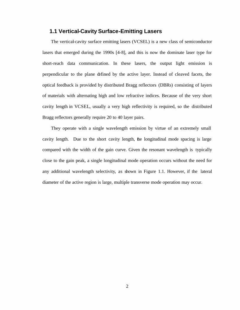
any additional wavelength selectivity, as shown in Figure 1.1. However, if the lateral
diameter of the active region is large, multiple transverse mode operation may occur.
3
Figure 1.1 Schematic showing the structural and spectral comparison between a vertical cavity surface emitting laser (VCSEL) and an edge emitting laser (EEL).
One of the particular advantages of VCSEL is that the spot size of the emission beam
can be made compatible with that of a single mode optical fiber, making the coupling
from a laser to the fiber easier and more efficient. In addition, the surface-emitting
geometry of the VCSEL structure enables wafer-scale fabrication and testing, which are
essential for low-cost volume manufacturing. Also, the monolithic structure of a VCSEL
makes it possible to fabricate very high density two-dimensional laser arrays. And
because of the short active region volume, VCSEL are among the most efficient
semiconductor diode lasers with extremely low threshold current and small power
consumption, which are critical for low-power consumer electronics applications.
Furthermore, a VCSEL can be directly modulated by varying its bias current, up to 30-40
GHz, which is very desirable in the application of digital and analog fiber-optic
communication systems [9].
4
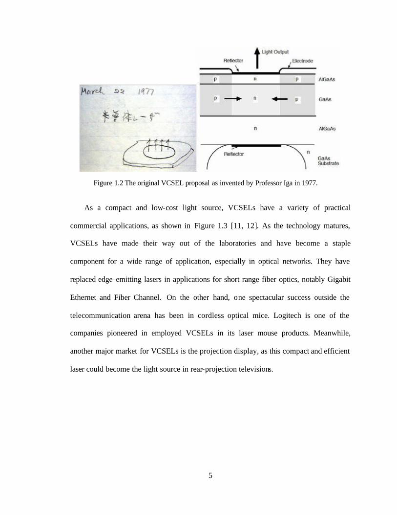
This practically new laser structure was invented by Prof. Kenichi Iga of Tokyo
Institute of Technology in 1977 [6, 10]. Figure 1.2 shows the original sketch of the first
proposed VCSEL idea. Two years later in 1979, the first device was experimentally
demonstrated operating in the pulsed operation at 77 K, where GaInAsP/InP material was
used for the active region with the emission wavelength at 1.3 µm. In 1986, a 6 mA-
threshold GaAs VCSEL as experimentally demonstrated. After the employment of metal
organic chemical vapor deposition (MOCVD) that enabled the growth of semiconductor
distributed Bragg reflectors, the first room temperature continuous wave VCSEL using
GaAs material was first demonstrated in 1987. Two years after, researchers from AT&T
Bell Laboratory demonstrated an InGaAs surface emitting laser exhibiting a 2 mA
threshold current, which was achieved by using ion implantation to efficiently confine the
electrical currents. These experiment results encouraged other groups to jump into the
research of vertical-cavity surface-emitting lasers. Soon after that, in 1990 sub-milliamp
threshold device was demonstrated, for the first time, by improving the active region
current confinement and the quality of the distributed Bragg reflectors.
Since 1992, VCSELs based on GaAs substrate have been extensively studied and
some of the 0.98, 0.85, and 0.78 µm wavelength devices are commercialized into optical
systems. In 1993, a 1.3 µm room temperature CW VCSEL was demonstrated. A wafer-
fusion technique enabled the operation at 1.55 µm at higher temperatures. In 1993, a
room temperature high performance CW red color InAlGaAs device was demonstrated.
In 1996, green-blue GaN based VCSEL research was started although the progress has
been much slower compare to VCSEL made of other materials.
5
Figure 1.2 The original VCSEL proposal as invented by Professor Iga in 1977.
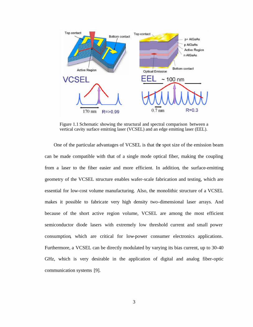
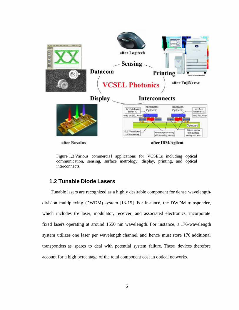
As a compact and low-cost light source, VCSELs have a variety of practical
commercial applications, as shown in Figure 1.3 [11, 12]. As the technology matures,
VCSELs have made their way out of the laboratories and have become a staple
component for a wide range of application, especially in optical networks. They have
replaced edge-emitting lasers in applications for short range fiber optics, notably Gigabit
Ethernet and Fiber Channel. On the other hand, one spectacular success outside the
telecommunication arena has been in cordless optical mice. Logitech is one of the
companies pioneered in employed VCSELs in its laser mouse products. Meanwhile,
another major market for VCSELs is the projection display, as this compact and efficient
laser could become the light source in rear-projection televisions.
6
Figure 1.3 Various commercia l applications for VCSELs including optical communication, sensing, surface metrology, display, printing, and optical interconnects.
1.2 Tunable Diode Lasers
Tunable lasers are recognized as a highly desirable component for dense wavelength-
division multiplexing (DWDM) system [13-15]. For instance, the DWDM transponder,
which includes the laser, modulator, receiver, and associated electronics, incorporate
fixed lasers operating at around 1550 nm wavelength. For instance, a 176-wavelength
system utilizes one laser per wavelength channel, and hence must store 176 additional
transponders as spares to deal with potential system failure. These devices therefore
account for a high percentage of the total component cost in optical networks.
7
Therefore, wavelength-tunable semiconductor diode lasers offer a very promising
and attractive alternative to the fixed-wavelength lasers. A single tunable laser module
can serve as a backup for multiple channels, so that fewer transponders need to be
stocked as spared. Consequently, this translates into cost-saving and simplification of the
entire sparing process and inventory management. Furthermore, tunable lasers are vital
for enabling the future intelligent optical networks, with applications in all-optical
switching and dynamically reconfigurable optical add-drop multiplexer.
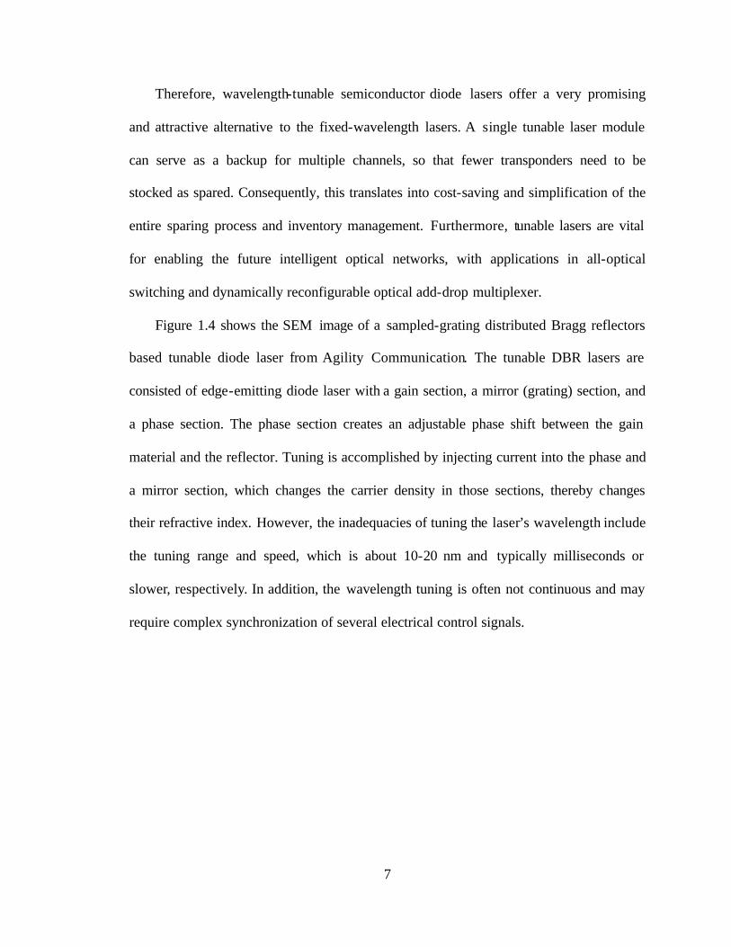
Figure 1.4 shows the SEM image of a sampled-grating distributed Bragg reflectors
based tunable diode laser from Agility Communication. The tunable DBR lasers are
consisted of edge-emitting diode laser with a gain section, a mirror (grating) section, and
a phase section. The phase section creates an adjustable phase shift between the gain
material and the reflector. Tuning is accomplished by injecting current into the phase and
a mirror section, which changes the carrier density in those sections, thereby changes
their refractive index. However, the inadequacies of tuning the laser’s wavelength include
the tuning range and speed, which is about 10-20 nm and typically milliseconds or
slower, respectively. In addition, the wavelength tuning is often not continuous and may
require complex synchronization of several electrical control signals.
8
Figure 1.4 SEM image of a tunable sample-grating distributed Bragg reflector diode laser from Agility Communications.
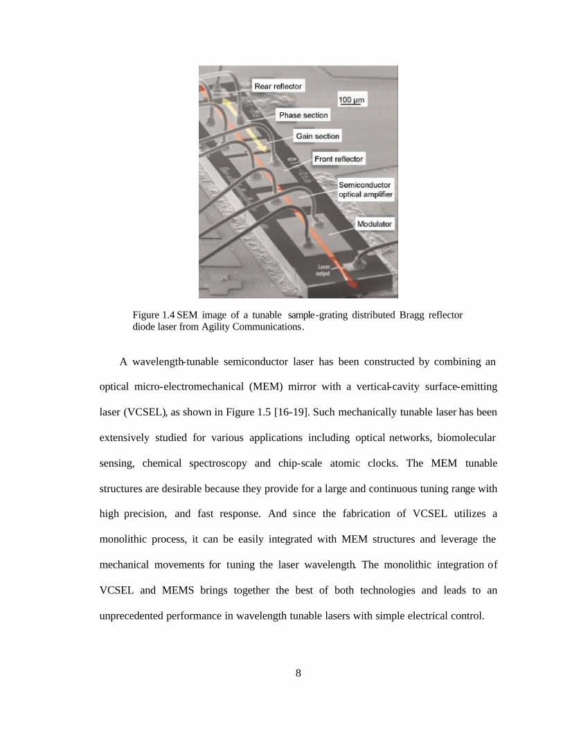
A wavelength-tunable semiconductor laser has been constructed by combining an
optical micro-electromechanical (MEM) mirror with a vertical-cavity surface-emitting
laser (VCSEL), as shown in Figure 1.5 [16-19]. Such mechanically tunable laser has been
extensively studied for various applications including optical networks, biomolecular
sensing, chemical spectroscopy and chip-scale atomic clocks. The MEM tunable
structures are desirable because they provide for a large and continuous tuning range with
high precision, and fast response. And since the fabrication of VCSEL utilizes a
monolithic process, it can be easily integrated with MEM structures and leverage the
mechanical movements for tuning the laser wavelength. The monolithic integration of
VCSEL and MEMS brings together the best of both technologies and leads to an
unprecedented performance in wavelength tunable lasers with simple electrical control.
9
Figure 1.5 SEM image of a micro-electromechanical tunable VCSEL.
The MEM tunable VCSEL has the majority part of its top mirror being held on a
micromechanical structure. Wavelength tuning is accomplished by applying a voltage
between the top DBR and bottom DBR, across the airgap. The applied bias generates the
electrostatic force, which attracts the top DBR downward toward the substrate. This
physical movement changes the optical length of the laser cavity and thus produces a
change (blue-shift) in the laser emission wavelength, as shown in Figure 1.6.
Figure 1.6 Schematic illustrating the operating principle of a wavelength-tunable micro-electromechanical VCSEL.
In terms of the device structure, the MEM tunable VCSEL have two pairs of electric
contacts, one for tuning the wavelength and the other for current injection, which can be
directly modulated at >10 Gb/s data rates. In addition, the MEM tunable VCSELs
10
maintains the essential benefits of VCSELs such as batch processing and wafer- level
testing, which are essential for low-cost volume manufacturability
1.3 Challenges in MEM Tunable VCSEL Research
Because of the short gain medium, broadband mirrors with high reflectivity are
essential for constructing a VCSEL cavity with a high quality-factor. This is critical for a
laser’s device performance since the reflectivity of the mirrors determines the threshold
current and output power of the device. However for the DBR based dielectric mirrors,
their reflectivity and bandwidth depend on the refractive index contrast of the constituent
materials and the precision of thickness control within each layer. Because of epitaxial
growth constraints for matching the material atomic lattice, typical combinations of DBR
materials often have small refractive index differences (?n<0.5). Hence often it is
necessary to require a rather large number of DBR pairs (25 – 40) to attain high enough
reflectivity (R>99.5%), in addition to the resulting small mirror bandwidth (??/??≈?3-9%).
This could be as thick as 4 µm and 10 µm for VCSELs emitting at 850 nm and 1.55 µm
wavelength, respectively.
Therefore, the growth of high-quality DBR mirrors has been one of the major
difficulties in the current status of VCSEL research, especially for those emitting at blue-
green and long infrared wavelengths [20-22]. The problem becomes more challenging for
making wavelength tunable VCSEL, where the requirements on the mirror bandwidth
and reflectivity are even more stringent [16, 23]. Furthermore, when integrating with
MEM structures, these rather thick DBR mirrors impose significant design limitations on
the length and width of the MEM structures. Thus, the mass of the movable mechanical
11
structures translates into a slow tuning speed, a limited tuning range, high actuation
power, as well as the epitaxial growth and processing difficulties.
1.4 Dissertation Overview
As a potential answer to the challenge motioned above, this dissertation present s a
novel surface emitting lasers utilizing a revolutionary, single- layer high- index-contrast
subwavelength grating (HCG), instead of the conventional distributed Bragg reflectors
mirror. The HCG provides both efficient optical feedback and control over the
wavelength and polarization of the emitted light. Such integration drastically reduces the
required VCSEL mirror epitaxial thickness and greatly simplifies the material growth and
fabrication process with a robust tolerance. Furthermore by integrating a mechanically
movable actuator with the single- layer HCG as the VCSEL top mirror, a wavelength
tunable laser can be obtained with precise and continuous tuning range. The small
footprint of HCG enables the scaling down of each of the mechanical actuator
dimensions, leading to >1000 times reduction in mass and increase in the mechanical
resonant frequency. Thus, a high-speed nano-electromechanical tunable VCSEL with
tens of nanoseconds tuning speed can be attained.
This dissertation is divided into the following sections. Chapter 2 is dedicated to the
introduction, design and preliminary optical characterization of the proposed highly
reflective high-contrast subwavelength grating mirrors. The grating presented is based on
a silicon-on-insulator design with the operating center wavelength is at 1.55 µm. Chapter
3 shows the development of a novel surface emitting laser incorporating the single- layer,
highly reflective high-contrast subwavelength grating instead of the conventional DBR.
Such integration resulted in a compact and efficient VCSEL with very desirable optical,
12
spectral and polarization properties. Chapter 4 shows the development of a novel high-
speed nano-electromechanical tunable VCSEL. By integrating a mechanically movable
actuator with the single-layer HCG as the VCSEL top mirror, precise and wide
continuous wavelength tuning was experimentally obtained with extremely fast, sub-100
nanoseconds tuning speed. Chapter 5 reports novel actuation mechanism utilizing the
inherent piezoelectric properties of the AlxGa1-xAs compounds for short-wavelength
MEMS tunable VCSEL. Piezoelectric actuation can provide precise mechanical
displacements with linear tuning characteristics, does not suffer from mechanical
deflection limitations, and most importantly eliminates the possibility of catastrophic
damages known for electrostatic actuation. Chapter 6 reports a novel application of a
tunable VCSEL in a highly sensitive, label- free biosensor for the detection and
monitoring of biomolecular interactions. This novel biosensor has demonstrated
sufficient sensitivity in a clinical-relevant assay, making it a potential new platform for
simplified and rapid point-of-care diagnostic tests for the detection of infectious diseases.
Finally in Chapter 7, the dissertation is summarized with some closing remarks.
13
Chapter 2 High Contrast Subwavelength Grating
2.1 Motivation
Broadband mirrors (??/? >15%) with very high reflectivity (R>99%) are essential for
semiconductor light emitting diodes and lasers, which are required to constructs optical
resonant cavity with a high quality-factor [24]. Metal mirrors have very wide reflection
bands, but the absorption of light introduces a large insertion loss that limits their use in
devices based on transmission. Semiconductor based distributed Bragg reflectors (DBRs)
have been utilized predominantly as the mirrors in most surface emitting lasers [25, 26].
Although the optical loss is lower compare to metallic mirrors, high precision in layer
thicknesses and the refractive indices in the material deposition are required to achieve
high reflectivity. Also limited by the small refractive index, typical DBRs require a large
number of pairs to achieve high reflectivity, which translates into difficulties in the
material epitaxial growth. Moreover, when scaling device to longer wavelengths, the
DBR thickness to be grown may become prohibitive (~20 µm per DBR mirror for ? = 10
14
µm). Furthermore, for the applications in tunable etalon type devices, such as micro-
electro-mechanical (MEM) vertical cavity surface emitting lasers (VCSEL), detectors and
optical filters, the mirror bandwidth and the resulting tuning range are limited to ??/? ≈?
3-9%. The challenge of designing mirror with broadband reflection, low loss and
compatibility with optoelectronic remains to be an important issue.
In this chapter we propose and experimentally demonstrate a novel single- layer high-
index-contrast subwavelength grating (HCG) that has >500 nm wide reflection bandwidth
(??/?~35%) from 1.12-1.6 2µm and very high reflectivity (>98.5%) [27, 28]. The design
of the subwavelength grating reflector is scalable for different wavelengths. It facilitates
monolithic integration of optoelectronic devices at a wide range of wavelengths from
visible to far infrared.
2.2 HCG Design
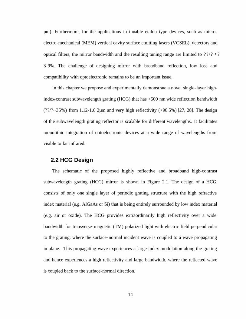
The schematic of the proposed highly reflective and broadband high-contrast
subwavelength grating (HCG) mirror is shown in Figure 2.1. The design of a HCG
consists of only one single layer of periodic grating structure with the high refractive
index material (e.g. AlGaAs or Si) that is being entirely surrounded by low index material
(e.g. air or oxide). The HCG provides extraordinarily high reflectivity over a wide
bandwidth for transverse-magnetic (TM) polarized light with electric field perpendicular
to the grating, where the surface-normal incident wave is coupled to a wave propagating
in-plane. This propagating wave experiences a large index modulation along the grating
and hence experiences a high reflectivity and large bandwidth, where the reflected wave
is coupled back to the surface-normal direction.
15
Here we introduce a silicon-on- insulator (SOI) based high-contrast subwavelength
grating. The grating layer comprises periodic rectangular silicon stripes spaced apart by
air, and it is sandwiched by air and silicon dioxide on the top and bottom, respective. For
practical consideration, a silicon substrate is used below the silicon dioxide. Generally,
the larger the refractive index contrast between the grating material and the surrounding
medium, the higher the reflectivity and larger the reflection bandwidth. The low index
layer under the grating is critical for the mirror effect. Design parameters for the structure
include the materials (index of refraction), thickness of the low index layer under the
grating (tL), grating period (Λ), grating thickness (tg) and grating duty cycle. Duty cycle is
defined as the ratio of the width of the high index material with respect to the period. In
the SOI HCG example that is designed for 1.55 um center wavelength, the parameters
are: nsubstrate = 3.48 (Si), nsuperstrate = 1 (air), nH = 3.48 (Poly-Si.), nL = 1 (air), nL = 1.47
(SiO2), Λ = 0.7 µm, tg = 0.46 µm and DC = 0.75.
Figure 2.1 Schematic of the high-contrast subwavelength grating reflector based on a silicon-on-insulator (SOI) wafer designed for 1.55 µm center wavelength.
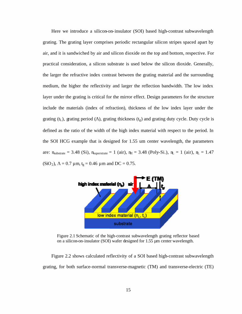
Figure 2.2 shows calculated reflectivity of a SOI based high-contrast subwavelength
grating, for both surface-normal transverse-magnetic (TM) and transverse-electric (TE)
16
polarized plane wave. The simulation is based on Rigorous Coupled Wave Analysis
(RCWA) [29], but we also have confirmed the calculation results by finite difference
time-domain (FDTD) methods [30, 31]. As shown in Figure 2.2, a very broadband mirror
with R>99% and ??/? > 30% is obtained around 1.55 µm, over the range 1.33 µm to 1.80
µm. For higher reflectivity requirement (R>99.9%), the mirror can still provide a very
large reflection bandwidth from 1.40-1.67 µm. In this calculation, the index of refraction
is assumed to be constant over the wavelength range and optical loss is not considered
(imaginary part of refractive index is 0), which is a reasonable approximation for the
considered wavelength range.
1 1.5 2 2.50
0.2
0.4
0.6
0.8
1
Wavelength (µm)
Ref
lect
ivity
TMTE
1.3 1.4 1.5 1.6 1.7 1.80.99
0.992
0.994
0.996
0.998
1
Wavelength (µm)
Ref
lect
ivity
(a) (b)
Figure 2.2 (a) Calculated reflectivity for a SOI-based high-contrast subwavelength grating, for TM and TE polarized incident plane wave. (b) Calculated reflection spectrum of the HCG for TM polarized light, with R>99%.
Since the grating contains one-dimensional symmetry, its optical property is
polarization dependent. This can be advantageous to control the polarization on a VCSEL,
e.g., if the grating design is used for the mirrors. If a 2D grating is chosen instead,
reflectivity would be polarization independent. The grating sensitivity to all these
17
parameters can be optimized iteratively. If the application has a less stringent requirement
on reflectivity, i.e. <99%, most of the parameters have a large tolerance range, sometimes
up to 10% variation. Experimental results are being carried on and will be presented soon.
It is interesting to note that the broadband reflectivity does not result from a
resonance, as the period of the grating is sub-wavelength but not half-wavelength.
Furthermore, the reflectivity spectrum can be scaled with wavelength. By simply
multiplying the dimensions by a constant, in this case 6.5, while keeping the other
parameters, the reflection band shifts to the 8.6-11.7 µm wavelength range with all
features and values being identical. Hence, any different wavelength regime can use the
same design. Note that the same constant has also multiplied the horizontal scale in order
to make the comparison easier. Although it may be obvious that any periodic structure
should be wavelength scalable, the scaling here is easily manufacturable since it only
requires changing the layer dimensions. Physical origins of the broadband reflection
phenomenon are under investigation.
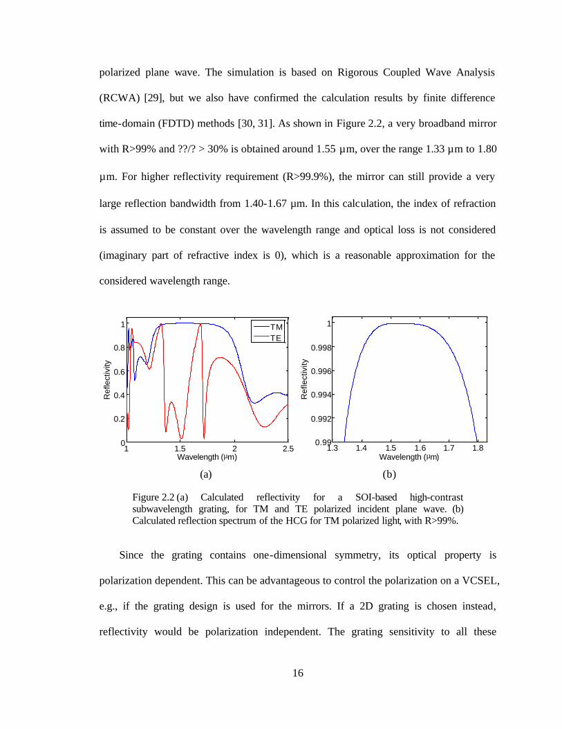
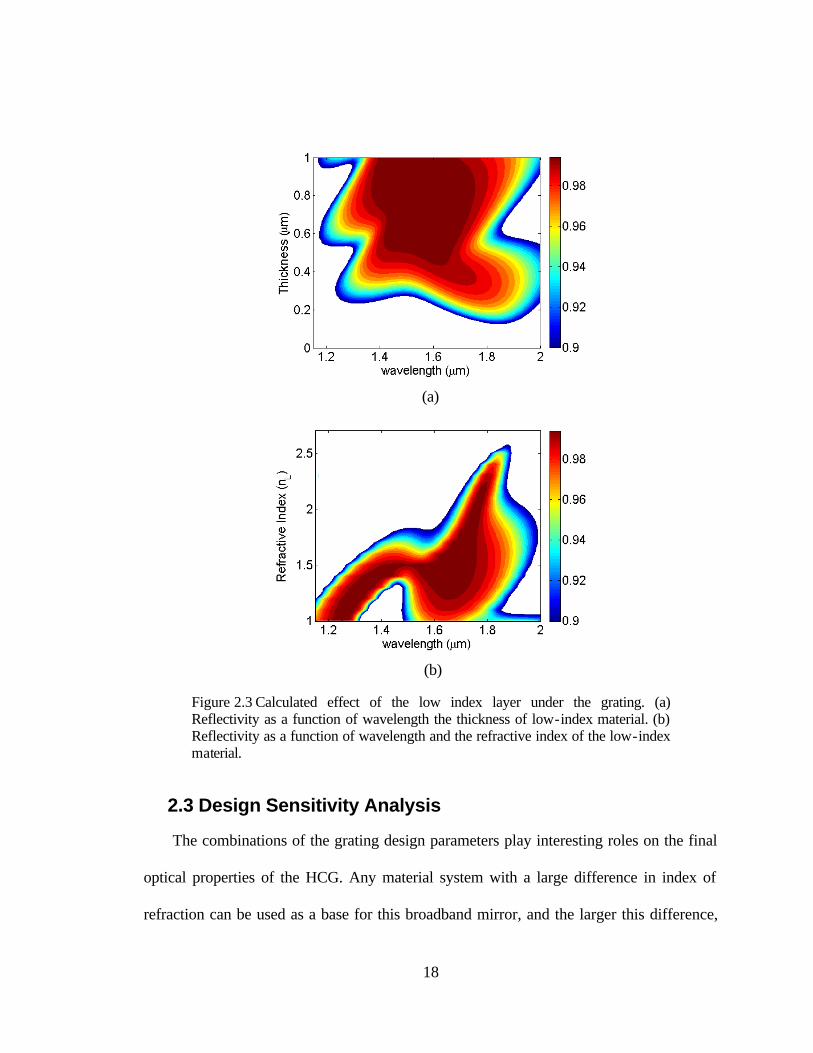
As mentioned earlier, the low index material layer under the grating is essential to
obtain the broadband reflection. Figure 2.3 shows the calculated reflectivity as a function
of the low-index material thickness and wavelength in a contour plot, where the y-axis
consists of the low-index material thickness (for a fixed nL) and refractive index (for a
fixed tL). Keeping all the other parameters the same, there is no reflection band for tL
<0.1 µm. Above this thickness, the structure has low sensitivity to the low index layer,
but this parameter can be used to optimize the reflection band. The mirror also does not
exist if nL >2.5. For instance if Si3N4 (n ≈ 2) were used instead of SiO 2, the result would
be a much smaller reflection band, ranging from 1.7µm to 1.8 µm.
18
(a)
(b)
Figure 2.3 Calculated effect of the low index layer under the grating. (a) Reflectivity as a function of wavelength the thickness of low-index material. (b) Reflectivity as a function of wavelength and the refractive index of the low-index material.
2.3 Design Sensitivity Analysis
The combinations of the grating design parameters play interesting roles on the final
optical properties of the HCG. Any material system with a large difference in index of
refraction can be used as a base for this broadband mirror, and the larger this difference,
19
the larger the band. Our simulations show results for silicon/air/SiO2, but GaAs/Al2O3,
GaN/air or ZnSe/CaF2 would be comparable. Thus, this grating is a potential candidate
for several active and passive optoelectronic devices. In the following discussion, we
show design sensitive analysis by varying one of the parameters at the time, while
keeping the others constant.
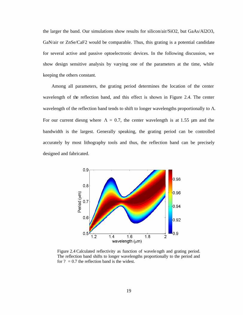
Among all parameters, the grating period determines the location of the center
wavelength of the reflection band, and this effect is shown in Figure 2.4. The center
wavelength of the reflection band tends to shift to longer wavelengths proportionally to Λ.
For our current diesng where Λ = 0.7, the center wavelength is at 1.55 µm and the
bandwidth is the largest. Generally speaking, the grating period can be controlled
accurately by most lithography tools and thus, the reflection band can be precisely
designed and fabricated.
Figure 2.4 Calculated reflectivity as function of wavelength and grating period. The reflection band shifts to longer wavelengths proportionally to the period and for ? = 0.7 the reflection band is the widest.
20
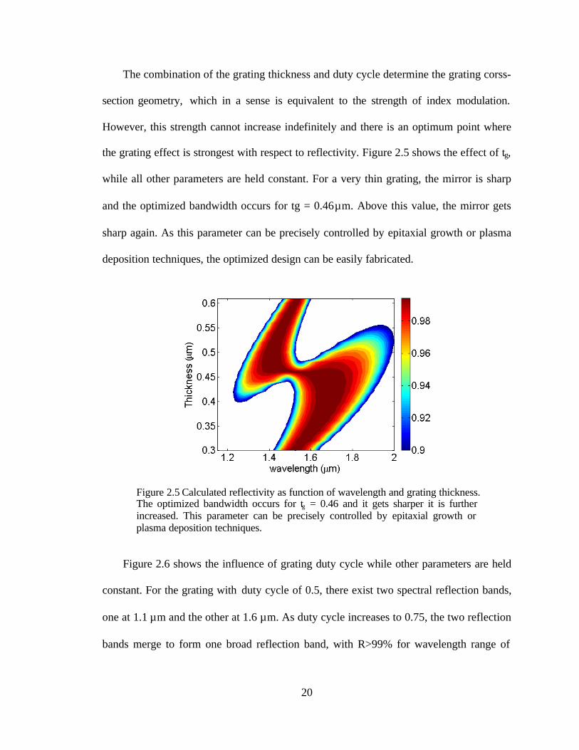
The combination of the grating thickness and duty cycle determine the grating corss-
section geometry, which in a sense is equivalent to the strength of index modulation.
However, this strength cannot increase indefinitely and there is an optimum point where
the grating effect is strongest with respect to reflectivity. Figure 2.5 shows the effect of tg,
while all other parameters are held constant. For a very thin grating, the mirror is sharp
and the optimized bandwidth occurs for tg = 0.46µm. Above this value, the mirror gets
sharp again. As this parameter can be precisely controlled by epitaxial growth or plasma
deposition techniques, the optimized design can be easily fabricated.
Figure 2.5 Calculated reflectivity as function of wavelength and grating thickness. The optimized bandwidth occurs for tg = 0.46 and it gets sharper it is further increased. This parameter can be precisely controlled by epitaxial growth or plasma deposition techniques.
Figure 2.6 shows the influence of grating duty cycle while other parameters are held
constant. For the grating with duty cycle of 0.5, there exist two spectral reflection bands,
one at 1.1 µm and the other at 1.6 µm. As duty cycle increases to 0.75, the two reflection
bands merge to form one broad reflection band, with R>99% for wavelength range of
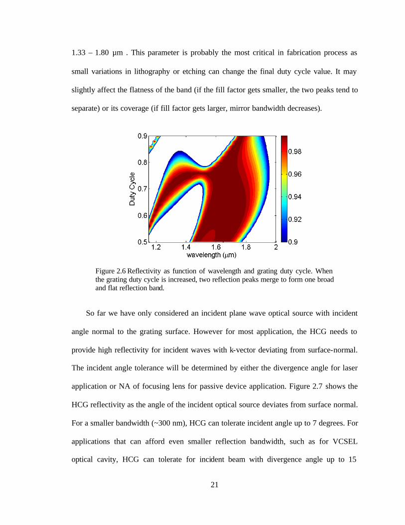
21
1.33 – 1.80 µm . This parameter is probably the most critical in fabrication process as
small variations in lithography or etching can change the final duty cycle value. It may
slightly affect the flatness of the band (if the fill factor gets smaller, the two peaks tend to
separate) or its coverage (if fill factor gets larger, mirror bandwidth decreases).
Figure 2.6 Reflectivity as function of wavelength and grating duty cycle. When the grating duty cycle is increased, two reflection peaks merge to form one broad and flat reflection band.
So far we have only considered an incident plane wave optical source with incident
angle normal to the grating surface. However for most application, the HCG needs to
provide high reflectivity for incident waves with k-vector deviating from surface-normal.
The incident angle tolerance will be determined by either the divergence angle for laser
application or NA of focusing lens for passive device application. Figure 2.7 shows the
HCG reflectivity as the angle of the incident optical source deviates from surface normal.
For a smaller bandwidth (~300 nm), HCG can tolerate incident angle up to 7 degrees. For
applications that can afford even smaller reflection bandwidth, such as for VCSEL
optical cavity, HCG can tolerate for incident beam with divergence angle up to 15
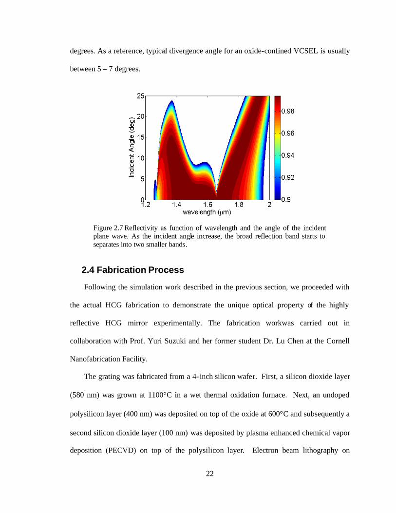
22
degrees. As a reference, typical divergence angle for an oxide-confined VCSEL is usually
between 5 – 7 degrees.
Figure 2.7 Reflectivity as function of wavelength and the angle of the incident plane wave. As the incident angle increase, the broad reflection band starts to separates into two smaller bands.
2.4 Fabrication Process
Following the simulation work described in the previous section, we proceeded with
the actual HCG fabrication to demonstrate the unique optical property of the highly
reflective HCG mirror experimentally. The fabrication workwas carried out in
collaboration with Prof. Yuri Suzuki and her former student Dr. Lu Chen at the Cornell
Nanofabrication Facility.
The grating was fabricated from a 4- inch silicon wafer. First, a silicon dioxide layer
(580 nm) was grown at 1100°C in a wet thermal oxidation furnace. Next, an undoped
polysilicon layer (400 nm) was deposited on top of the oxide at 600°C and subsequently a
second silicon dioxide layer (100 nm) was deposited by plasma enhanced chemical vapor
deposition (PECVD) on top of the polysilicon layer. Electron beam lithography on
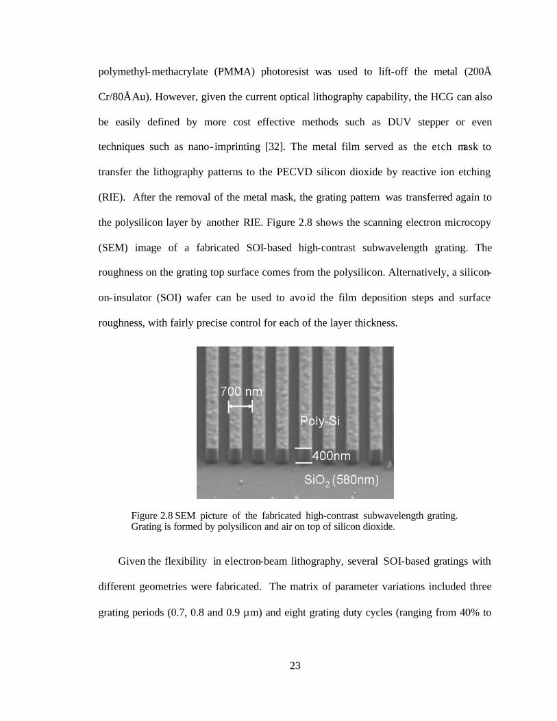
23
polymethyl-methacrylate (PMMA) photoresist was used to lift-off the metal (200Å
Cr/80Å Au). However, given the current optical lithography capability, the HCG can also
be easily defined by more cost effective methods such as DUV stepper or even
techniques such as nano- imprinting [32]. The metal film served as the etch mask to
transfer the lithography patterns to the PECVD silicon dioxide by reactive ion etching
(RIE). After the removal of the metal mask, the grating pattern was transferred again to
the polysilicon layer by another RIE. Figure 2.8 shows the scanning electron microcopy
(SEM) image of a fabricated SOI-based high-contrast subwavelength grating. The
roughness on the grating top surface comes from the polysilicon. Alternatively, a silicon-
on- insulator (SOI) wafer can be used to avo id the film deposition steps and surface
roughness, with fairly precise control for each of the layer thickness.
Figure 2.8 SEM picture of the fabricated high-contrast subwavelength grating. Grating is formed by polysilicon and air on top of silicon dioxide.
Given the flexibility in electron-beam lithography, several SOI-based gratings with
different geometries were fabricated. The matrix of parameter variations included three
grating periods (0.7, 0.8 and 0.9 µm) and eight grating duty cycles (ranging from 40% to
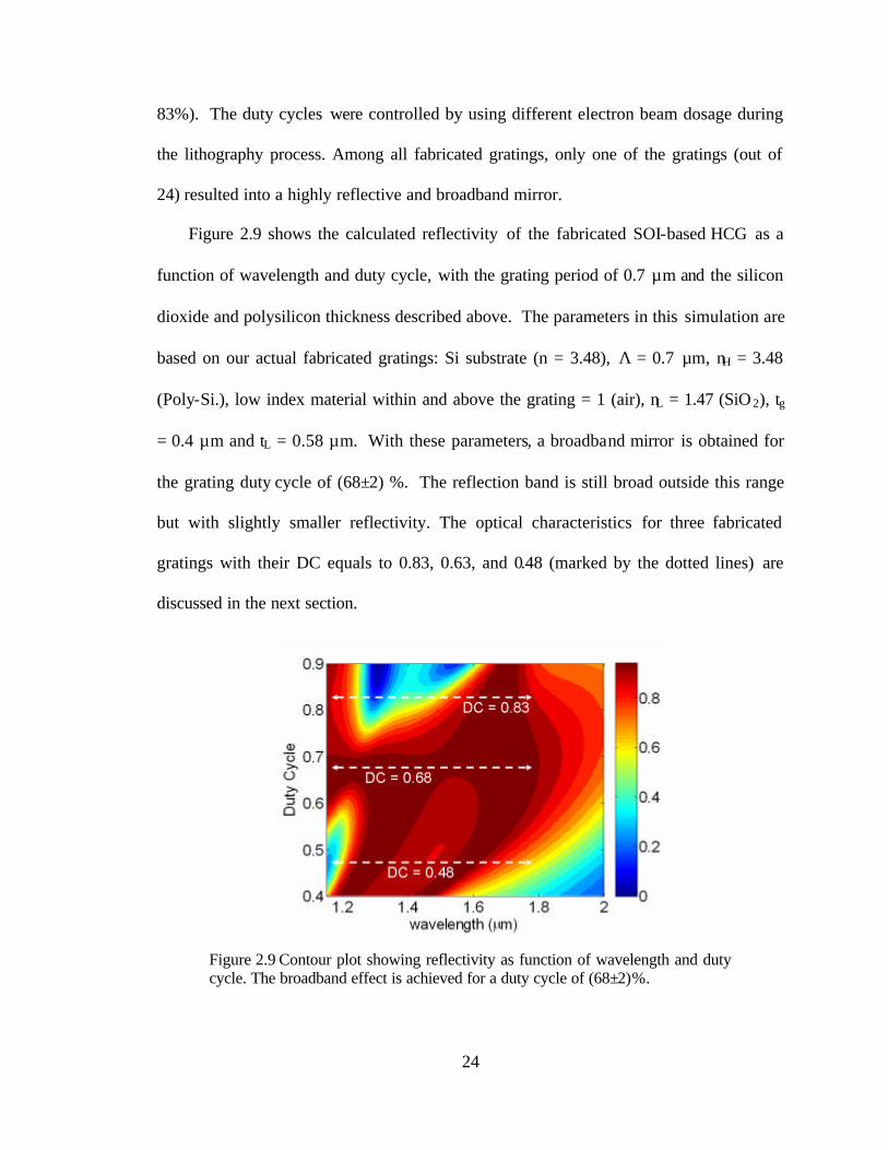
24
83%). The duty cycles were controlled by using different electron beam dosage during
the lithography process. Among all fabricated gratings, only one of the gratings (out of
24) resulted into a highly reflective and broadband mirror.
Figure 2.9 shows the calculated reflectivity of the fabricated SOI-based HCG as a
function of wavelength and duty cycle, with the grating period of 0.7 µm and the silicon
dioxide and polysilicon thickness described above. The parameters in this simulation are
based on our actual fabricated gratings: Si substrate (n = 3.48), Λ = 0.7 µm, nH = 3.48
(Poly-Si.), low index material within and above the grating = 1 (air), nL = 1.47 (SiO 2), tg
= 0.4 µm and tL = 0.58 µm. With these parameters, a broadband mirror is obtained for
the grating duty cycle of (68±2) %. The reflection band is still broad outside this range
but with slightly smaller reflectivity. The optical characteristics for three fabricated
gratings with their DC equals to 0.83, 0.63, and 0.48 (marked by the dotted lines) are
discussed in the next section.
Figure 2.9 Contour plot showing reflectivity as function of wavelength and duty cycle. The broadband effect is achieved for a duty cycle of (68±2)%.
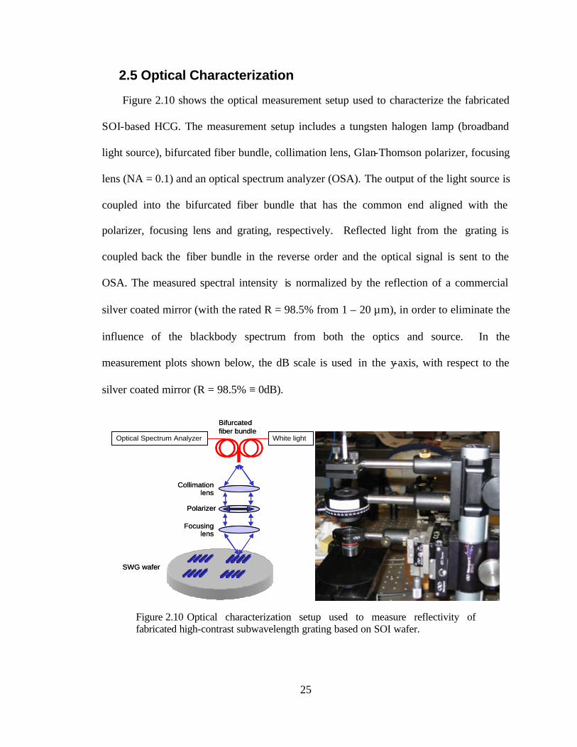
25
2.5 Optical Characterization
Figure 2.10 shows the optical measurement setup used to characterize the fabricated
SOI-based HCG. The measurement setup includes a tungsten halogen lamp (broadband
light source), bifurcated fiber bundle, collimation lens, Glan-Thomson polarizer, focusing
lens (NA = 0.1) and an optical spectrum analyzer (OSA). The output of the light source is
coupled into the bifurcated fiber bundle that has the common end aligned with the
polarizer, focusing lens and grating, respectively. Reflected light from the grating is
coupled back the fiber bundle in the reverse order and the optical signal is sent to the
OSA. The measured spectral intensity is normalized by the reflection of a commercial
silver coated mirror (with the rated R = 98.5% from 1 – 20 µm), in order to eliminate the
influence of the blackbody spectrum from both the optics and source. In the
measurement plots shown below, the dB scale is used in the y-axis, with respect to the
silver coated mirror (R = 98.5% ≡ 0dB).
SWG wafer
Bifurcated fiber bundle
Collimation lens
Optical Spectrum Analyzer
Polarizer
Focusing lens
White light
SWG wafer
Bifurcated fiber bundle
Collimation lens
Optical Spectrum Analyzer
Polarizer
Focusing lens
White light
Figure 2.10 Optical characterization setup used to measure reflectivity of fabricated high-contrast subwavelength grating based on SOI wafer.
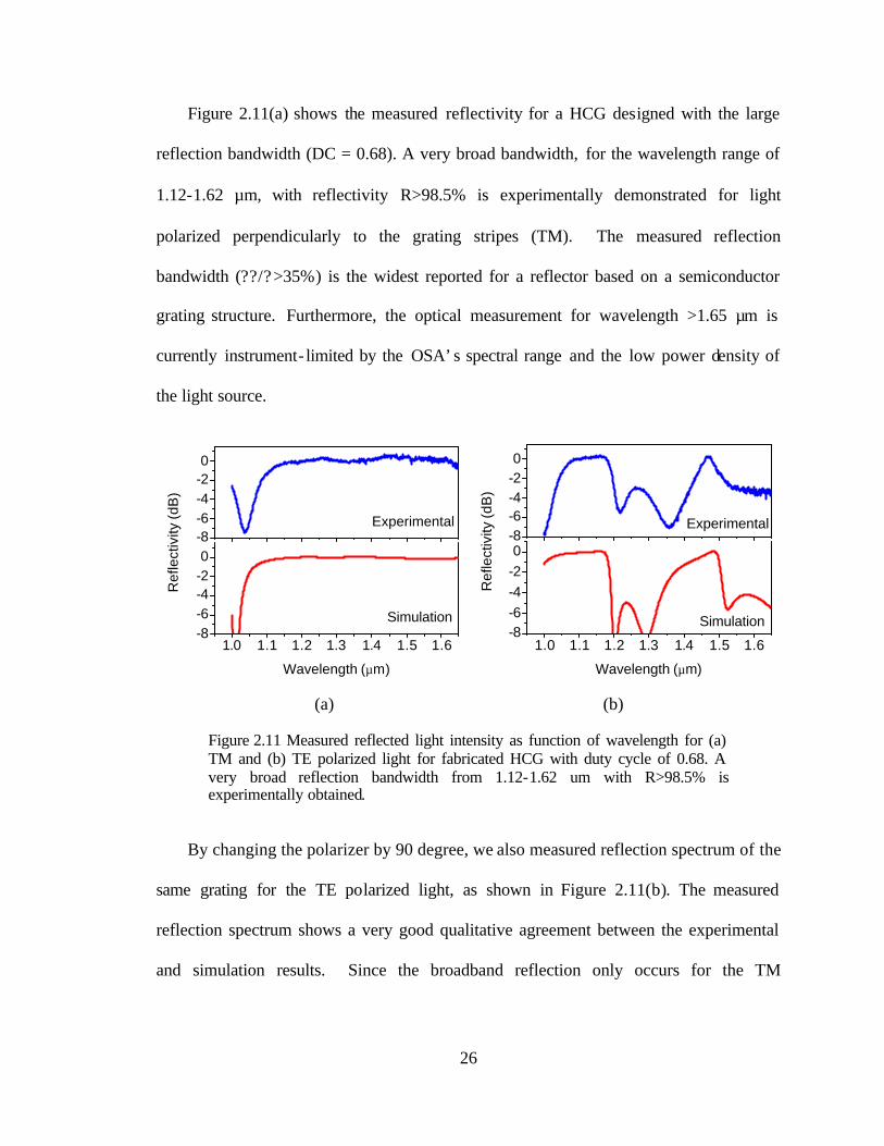
26
Figure 2.11(a) shows the measured reflectivity for a HCG designed with the large
reflection bandwidth (DC = 0.68). A very broad bandwidth, for the wavelength range of
1.12-1.62 µm, with reflectivity R>98.5% is experimentally demonstrated for light
polarized perpendicularly to the grating stripes (TM). The measured reflection
bandwidth (??/?>35%) is the widest reported for a reflector based on a semiconductor
grating structure. Furthermore, the optical measurement for wavelength >1.65 µm is
currently instrument- limited by the OSA’s spectral range and the low power density of
the light source.
1.0 1.1 1.2 1.3 1.4 1.5 1.6-8-6-4-20
Ref
lect
ivity
(dB
)
Wavelength (µm)
Experimental
Simulation
-8-6-4-20
1.0 1.1 1.2 1.3 1.4 1.5 1.6-8-6-4-20
Ref
lect
ivity
(dB
)
Wavelength (µm)
-8-6-4-20
Experimental
Simulation
(a) (b)
Figure 2.11 Measured reflected light intensity as function of wavelength for (a) TM and (b) TE polarized light for fabricated HCG with duty cycle of 0.68. A very broad reflection bandwidth from 1.12-1.62 um with R>98.5% is experimentally obtained.
By changing the polarizer by 90 degree, we also measured reflection spectrum of the
same grating for the TE polarized light, as shown in Figure 2.11(b). The measured
reflection spectrum shows a very good qualitative agreement between the experimental
and simulation results. Since the broadband reflection only occurs for the TM
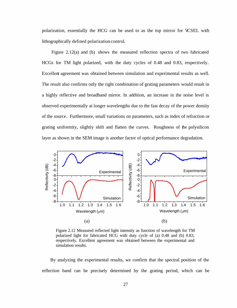
27
polarization, essentially the HCG can be used to as the top mirror for VCSEL with
lithographically defined polarization control.
Figure 2.12(a) and (b) shows the measured reflection spectra of two fabricated
HCGs for TM light polarized, with the duty cycles of 0.48 and 0.83, respectively.
Excellent agreement was obtained between simulation and experimental results as well.
The result also confirms only the right combination of grating parameters would result in
a highly reflective and broadband mirror. In addition, an increase in the noise level is
observed experimentally at longer wavelengths due to the fast decay of the power density
of the source. Furthermore, small variations on parameters, such as index of refraction or
grating uniformity, slightly shift and flatten the curves. Roughness of the polysilicon
layer as shown in the SEM image is another factor of optical performance degradation.
1.0 1.1 1.2 1.3 1.4 1.5 1.6-8-6-4-20
Ref
lect
ivity
(dB
)
Wavelength (µm)
-8-6-4-20
Simulation
Experimental
1.0 1.1 1.2 1.3 1.4 1.5 1.6-8-6-4-20
Ref
lect
ivity
(dB
)
Wavelength (µm)
-8-6-4-20
Experimental
Simulation
(a) (b)
Figure 2.12 Measured reflected light intensity as function of wavelength for TM polarized light for fabricated HCG with duty cycle of (a) 0.48 and (b) 0.83, respectively. Excellent agreement was obtained between the experimental and simulation results.
By analyzing the experimental results, we confirm that the spectral position of the
reflection band can be precisely determined by the grating period, which can be
28
controlled accurately by most lithography tools. The grating duty cycle is the most
critical parameter in the fabrication process, since a small variation in the lithography
exposure cond ition and/or etching can perturb the final grating geometries. Of course,
both the grating and oxide thicknesses are also critical, but once these values are known,
the other parameters (period and duty cycle) can be designed and adjusted accordingly.
2.6 Bandwidth and Tolerance Trade-Off
From the optical characterization of the fabricated SOI-based HCG, we noticed the
main contributing factors for process variations are mainly the film deposition and
etching steps, which affect the final grating thickness and its geometrical profile.
Lithography, which determines the grating period and duty cycle, can be assumed to be
ideal given the capabilities of current state-of-art lithographical technology.
A dielectric thin film deposition step is required to form the grating material with a
specific thickness. Figure 2.5 shows the effects of different grating thickness on the
reflectivity on HCG. For applications that require an ultra-broadband reflectivity,
material thickness needs to be precisely controlled (in our optimal design = 0.41 µm),
perhaps by an epitaxy technology. However, the thickness precision can be greatly
relaxed (0.35-0.5 µm) when reducing the bandwidth requirement to be around 200 nm for
center wavelength of 1.65 µm. Contrary to the grating high- index material, the low-index
material underneath the grating, which forms the cladding layer for the grating
waveguide, has very large tolerance for its thickness variations.
After the lithography process, an etching process is needed to transfer the patterns
from photoresist to the grating layer. However, the imperfection of the etch step often
results in grating geometry deviating from the ideal rectangular profile used in
29
simulations. For instance, a chemical based dry etching technique is generally isotropic,
which may result in a trapezoidal grating profile as the result of side-wall etching. Figure
2.13 illustrates effects of the isotropic etch on the reflectivity of a SOI-based HCG. The
contour plot shows reflectivity as a function of the wavelength and ratio a1/a0, where this
ratio is related to the degree of trapezoidal profile due to isotropic etches. Here, a1 and a2
are defined as the top and bottom base width of the resulting grating profiles after
fabrication, respectively, while a0 is the ideal designed width. With an anisotropic etch
(a1/a0 = 1), there is a very broad R>99% reflectivity bandwidth from 1.2-1.65 µm,
resulting from the rectangular grating profile. As the degree of isotropic etches increases,
the high reflective bandwidth reduces. In the extreme case that the grating profile
becomes triangular (a1/a0 = 0), the highly reflective spectrum is greatly compromised as
the consequence of the triangular grating profile. However, for applications where the
mirror bandwidth can be reduced to 150 nm centered at 1.55 µm wavelength (such as
wavelength tunable optical filter), the HCG can tolerate the trapezoidal grating profile
with the ratio a1/a0>0.5, yet is still able to provide the >99% reflectivity. Figure 2.13(b)
shows the reflection spectra for a few ratios of a1/a0, illustrating the insensitivity of
reflectivity from 1.48 – 1.63µm.
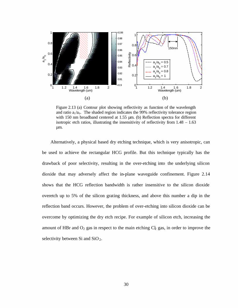
30
1 1.2 1.4 1.6 1.8 20
0.2
0.4
0.6
0.8
1
Wavelength (um)
a 1/a
0
<0.9
0.91
0.92
0.93
0.94
0.95
0.96
0.97
0.98
>0.99
1 1.2 1.4 1.6 1.8 20
0.2
0.4
0.6
0.8
1
Wavelength (um)
a 1/a
0
<0.9
0.91
0.92
0.93
0.94
0.95
0.96
0.97
0.98
>0.99
1 1.2 1.4 1.6 1.8 2 0
0.2
0.4
0.6
0.8
1
Wavelength (um)
Ref
lect
ivity
a1/a0 = 0.5a
1/a
0 = 0.7
a1/a
0 = 0.8
a1/a0 = 1
150nm
1 1.2 1.4 1.6 1.8 2 0
0.2
0.4
0.6
0.8
1
Wavelength (um)
Ref
lect
ivity
a1/a0 = 0.5a
1/a
0 = 0.7
a1/a
0 = 0.8
a1/a0 = 1
150nm
(a) (b)
Figure 2.13 (a) Contour plot showing reflectivity as function of the wavelength and ratio a1/a0. The shaded region indicates the 99% reflectivity tolerance region with 150 nm broadband centered at 1.55 µm. (b) Reflection spectra for different isotropic etch ratios, illustrating the insensitivity of reflectivity from 1.48 – 1.63 µm.
Alternatively, a physical based dry etching technique, which is very anisotropic, can
be used to achieve the rectangular HCG profile. But this technique typically has the
drawback of poor selectivity, resulting in the over-etching into the underlying silicon
dioxide that may adversely affect the in-plane waveguide confinement. Figure 2.14
shows that the HCG reflection bandwidth is rather insensitive to the silicon dioxide
overetch up to 5% of the silicon grating thickness, and above this number a dip in the
reflection band occurs. However, the problem of over-etching into silicon dioxide can be
overcome by optimizing the dry etch recipe. For example of silicon etch, increasing the
amount of HBr and O2 gas in respect to the main etching Cl2 gas, in order to improve the
selectivity between Si and SiO 2.
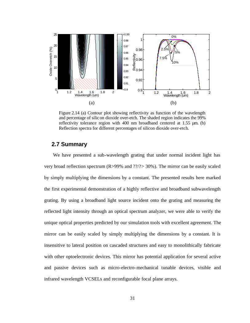
31
1 1.2 1.4 1.6 1.8 2 0
5
10
15
20
25
Oxi
de O
vere
tch
(%)
Wavelength (um)
<0.9
0.91
0.92
0.93
0.94
0.95
0.96
0.97
0.98
>0.99
1 1.2 1.4 1.6 1.8 2 0
5
10
15
20
25
Oxi
de O
vere
tch
(%)
Wavelength (um)
<0.9
0.91
0.92
0.93
0.94
0.95
0.96
0.97
0.98
>0.99
1 1.2 1.4 1.6 1.8 20.9
0.92
0.94
0.96
0.98
1
Wavelength (um)
Ref
lect
ivity
0%2.5%5%7.5%10%
10%7.5%
5%
0%
2.5%
1 1.2 1.4 1.6 1.8 20.9
0.92
0.94
0.96
0.98
1
Wavelength (um)
Ref
lect
ivity
0%2.5%5%7.5%10%
10%7.5%
5%
0%
2.5%
(a) (b)
Figure 2.14 (a) Contour plot showing reflectivity as function of the wavelength and percentage of silicon dioxide over-etch. The shaded region indicates the 99% reflectivity tolerance region with 400 nm broadband centered at 1.55 µm. (b) Reflection spectra for different percentages of silicon dioxide over-etch.
2.7 Summary
We have presented a sub-wavelength grating that under normal incident light has
very broad reflection spectrum (R>99% and ??/?> 30%). The mirror can be easily scaled
by simply multiplying the dimensions by a constant. The presented results here marked
the first experimental demonstration of a highly reflective and broadband subwavelength
grating. By using a broadband light source incident onto the grating and measuring the
reflected light intensity through an optical spectrum analyzer, we were able to verify the
unique optical properties predicted by our simulation tools with excellent agreement. The
mirror can be easily scaled by simply multiplying the dimensions by a constant. It is
insensitive to lateral position on cascaded structures and easy to monolithically fabricate
with other optoelectronic devices. This mirror has potential application for several active
and passive devices such as micro-electro-mechanical tunable devices, visible and
infrared wavelength VCSELs and reconfigurable focal plane arrays.
32
Chapter 3 High-Contrast Subwavelength Grating VCSEL
3.1 Motivation
Broadband mirrors with high reflectivity are essential for constructing a VCSEL
cavity with a high quality-factor. They are typically composed of semiconductor
distributed Bragg reflectors (DBRs), structures formed from multiple layers of alternating
dielectric materials with periodic variation of refractive indices. Their reflectivity and
bandwidth depend on the refractive index contrast of the constituent materials and the
precision of thickness control within each layer. Because of epitaxial growth constraints
for matching the material atomic lattice, typical combinations of DBR materials often
have small refractive index differences (nH/nL < 1.2). Thus, often it is necessary to require
a rather large number of DBR pairs (25–40) to attain high enough reflectivity, in addition
to the resulting small mirror bandwidth (??/? = 3–9%). This has been one of the major
difficulties in the current status of VCSEL fabrication, especially for blue-green and long
infrared wavelengths. The problem becomes more challenging for making wavelength-
33
tunable VCSELs, where the requirements on mirror bandwidth and reflectivity are even
more stringent.
In the previous chapter, we proposed and demonstrated a single- layer, high- index-
contrast subwavelength grating (HCG), which serves as a solution to overcome the
limitation of distributed Bragg reflectors in surface-emitting optoelectronic devices, For
instance, a 35-40 pairs of GaAs/AlGaAs DBRs (thickness of ~5 µm) can be replaced by
an AlGaAs based HCG (thickness of 0.235 µm) with the equivalent reflectivity. Thus,
HCG can potentially reduce the required VCSEL mirror epitaxial thickness and
simplifies material growth requirements for the thickness and composition accuracy. The
HCG is different from a second-order grating both in terms of structural design and
performance, whose coupling efficiency and reflectivity are both significantly lower.
Furthermore, the HCG reflectivity bandwidth is 10 and 100 times wider than that of
conventional DBRs and second order gratings, respectively.
Previously, we reported theoretical calculations and experimental reflectivity
measurements of a single HCG mirror. However, it was difficult to determine the
absolute value of the reflectivity, the phase delay, and the dependence on beam
divergence, which are all critical for VCSEL design. As such, it was uncertain whether
an HCG was suitable to integrate with a VCSEL structure to be used in the near-field
regime. In this chapter, we present a vertical-cavity surface-emitting laser (HCG
VCSEL) that incorporate a single-layer high- index-contrast subwavelength grating as the
top reflector in its optical cavity. The HCG provides both efficient optical feedback and
control over the wavelength and polarization of the emitted light. Such integration results
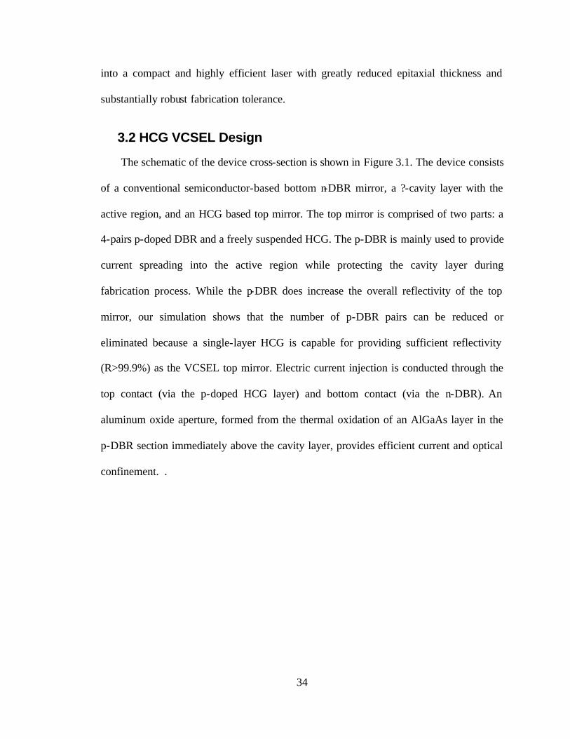
34
into a compact and highly efficient laser with greatly reduced epitaxial thickness and
substantially robust fabrication tolerance.
3.2 HCG VCSEL Design
The schematic of the device cross-section is shown in Figure 3.1. The device consists
of a conventional semiconductor-based bottom n-DBR mirror, a ?-cavity layer with the
active region, and an HCG based top mirror. The top mirror is comprised of two parts: a
4-pairs p-doped DBR and a freely suspended HCG. The p-DBR is mainly used to provide
current spreading into the active region while protecting the cavity layer during
fabrication process. While the p-DBR does increase the overall reflectivity of the top
mirror, our simulation shows that the number of p-DBR pairs can be reduced or
eliminated because a single-layer HCG is capable for providing sufficient reflectivity
(R>99.9%) as the VCSEL top mirror. Electric current injection is conducted through the
top contact (via the p-doped HCG layer) and bottom contact (via the n-DBR). An
aluminum oxide aperture, formed from the thermal oxidation of an AlGaAs layer in the
p-DBR section immediately above the cavity layer, provides efficient current and optical
confinement. .
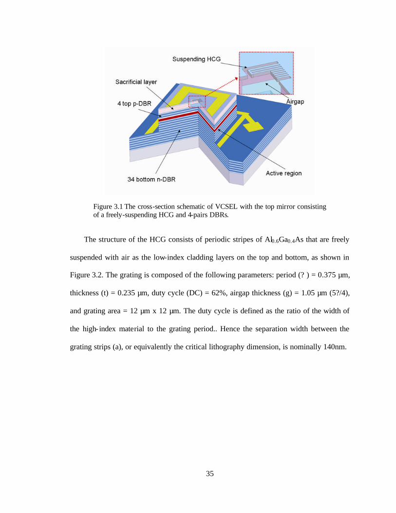
35
Figure 3.1 The cross-section schematic of VCSEL with the top mirror consisting of a freely-suspending HCG and 4-pairs DBRs.
The structure of the HCG consists of periodic stripes of Al0.6Ga0.4As that are freely
suspended with air as the low-index cladding layers on the top and bottom, as shown in
Figure 3.2. The grating is composed of the following parameters: period (? ) = 0.375 µm,
thickness (t) = 0.235 µm, duty cycle (DC) = 62%, airgap thickness (g) = 1.05 µm (5?/4),
and grating area = 12 µm x 12 µm. The duty cycle is defined as the ratio of the width of
the high- index material to the grating period.. Hence the separation width between the
grating strips (a), or equivalently the critical lithography dimension, is nominally 140nm.
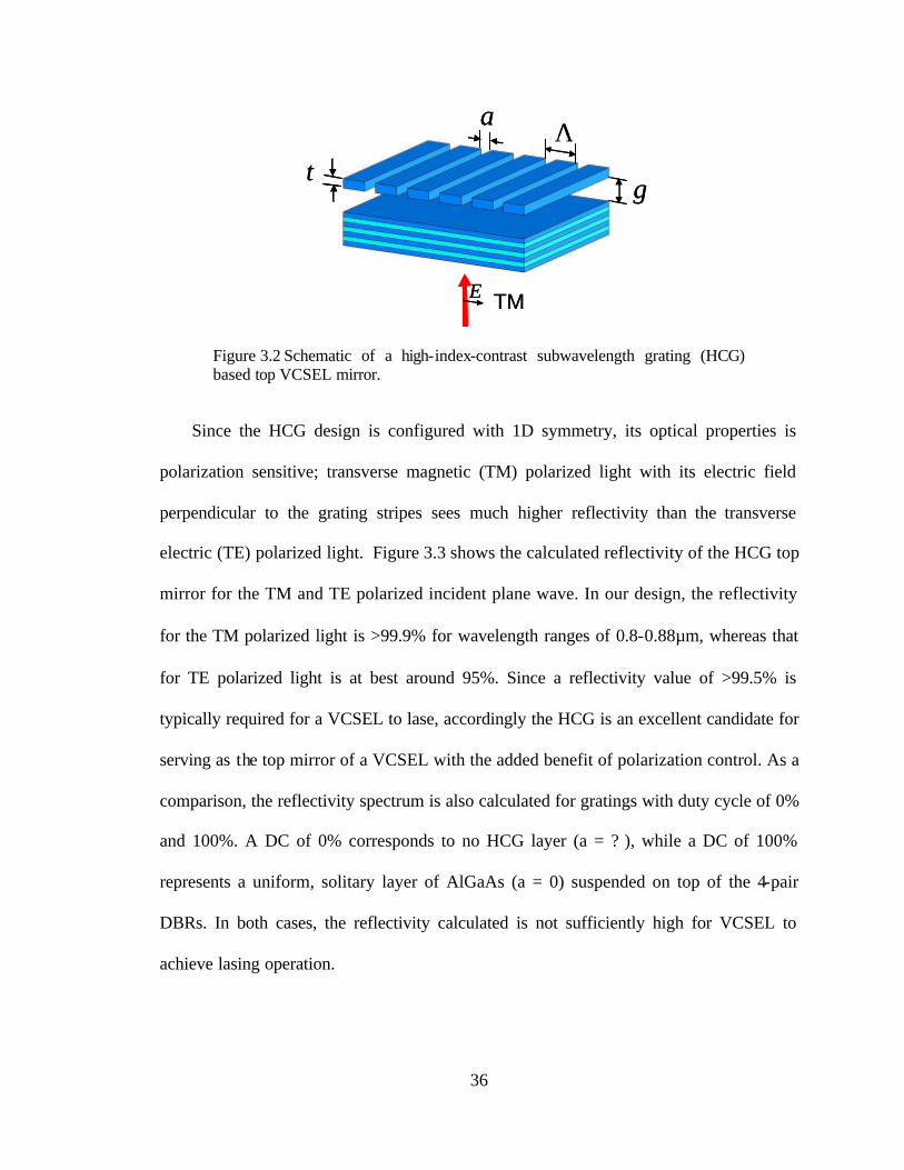
36
Λa
tg
E TM
Λa
tg
E TM
Figure 3.2 Schematic of a high-index-contrast subwavelength grating (HCG) based top VCSEL mirror.
Since the HCG design is configured with 1D symmetry, its optical properties is
polarization sensitive; transverse magnetic (TM) polarized light with its electric field
perpendicular to the grating stripes sees much higher reflectivity than the transverse
electric (TE) polarized light. Figure 3.3 shows the calculated reflectivity of the HCG top
mirror for the TM and TE polarized incident plane wave. In our design, the reflectivity
for the TM polarized light is >99.9% for wavelength ranges of 0.8-0.88µm, whereas that
for TE polarized light is at best around 95%. Since a reflectivity value of >99.5% is
typically required for a VCSEL to lase, accordingly the HCG is an excellent candidate for
serving as the top mirror of a VCSEL with the added benefit of polarization control. As a
comparison, the reflectivity spectrum is also calculated for gratings with duty cycle of 0%
and 100%. A DC of 0% corresponds to no HCG layer (a = ? ), while a DC of 100%
represents a uniform, solitary layer of AlGaAs (a = 0) suspended on top of the 4-pair
DBRs. In both cases, the reflectivity calculated is not sufficiently high for VCSEL to
achieve lasing operation.
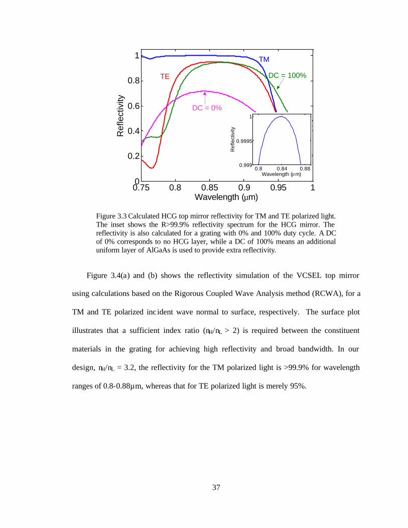
37
0.75 0.8 0.85 0.9 0.95 10
0.2
0.4
0.6
0.8
1
Wavelength (µm)
Ref
lect
ivity
0.8 0.84 0.880.999
0.9995
1
Wavelength (µm)
Ref
lect
ivity
TM
TE
DC = 0%
DC = 100%
0.75 0.8 0.85 0.9 0.95 10
0.2
0.4
0.6
0.8
1
Wavelength (µm)
Ref
lect
ivity
0.8 0.84 0.880.999
0.9995
1
Wavelength (µm)
Ref
lect
ivity
TM
TE
DC = 0%
DC = 100%
Figure 3.3 Calculated HCG top mirror reflectivity for TM and TE polarized light. The inset shows the R>99.9% reflectivity spectrum for the HCG mirror. The reflectivity is also calculated for a grating with 0% and 100% duty cycle. A DC of 0% corresponds to no HCG layer, while a DC of 100% means an additional uniform layer of AlGaAs is used to provide extra reflectivity.
Figure 3.4(a) and (b) shows the reflectivity simulation of the VCSEL top mirror
using calculations based on the Rigorous Coupled Wave Analysis method (RCWA), for a
TM and TE polarized inc ident wave normal to surface, respectively. The surface plot
illustrates that a sufficient index ratio (nH/nL > 2) is required between the constituent
materials in the grating for achieving high reflectivity and broad bandwidth. In our
design, nH/nL = 3.2, the reflectivity for the TM polarized light is >99.9% for wavelength
ranges of 0.8-0.88µm, whereas that for TE polarized light is merely 95%.
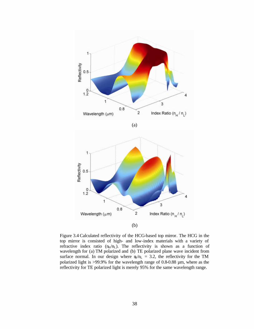
38
(a)
(b)
Figure 3.4 Calculated reflectivity of the HCG-based top mirror. The HCG in the top mirror is consisted of high- and low-index materials with a variety of refractive index ratio (nH/nL). The reflectivity is shown as a function of wavelength for (a) TM polarized and (b) TE polarized plane wave incident from surface normal. In our design where nH/nL = 3.2, the reflectivity for the TM polarized light is >99.9% for the wavelength range of 0.8-0.88 µm, where as the reflectivity for TE polarized light is merely 95% for the same wavelength range.
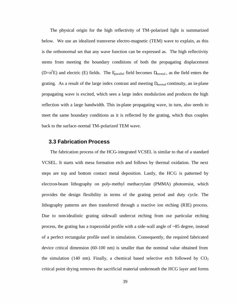
39
The physical origin for the high reflectivity of TM-polarized light is summarized
below. We use an idealized transverse electro-magnetic (TEM) wave to explain, as this
is the orthonormal set that any wave function can be expressed as. The high reflectivity
stems from meeting the boundary conditions of both the propagating displacement
(D=n2E) and electric (E) fields. The Eparallel field becomes Dnormal., as the field enters the
grating. As a result of the large index contrast and meeting Dnormal continuity, an in-plane
propagating wave is excited, which sees a large index modula tion and produces the high
reflection with a large bandwidth. This in-plane propagating wave, in turn, also needs to
meet the same boundary conditions as it is reflected by the grating, which thus couples
back to the surface-normal TM-polarized TEM wave.
3.3 Fabrication Process
The fabrication process of the HCG-integrated VCSEL is similar to that of a standard
VCSEL. It starts with mesa formation etch and follows by thermal oxidation. The next
steps are top and bottom contact metal deposition. Lastly, the HCG is patterned by
electron-beam lithography on poly-methyl methacrylate (PMMA) photoresist, which
provides the design flexibility in terms of the grating period and duty cycle. The
lithography patterns are then transferred through a reactive ion etching (RIE) process.
Due to non-idealistic grating sidewall undercut etching from our particular etching
process, the grating has a trapezoidal profile with a side-wall angle of ~85 degree, instead
of a perfect rectangular profile used in simulation. Consequently, the required fabricated
device critical dimension (60-100 nm) is smaller than the nominal value obtained from
the simulation (140 nm). Finally, a chemical based selective etch followed by CO2
critical point drying removes the sacrificial material underneath the HCG layer and forms
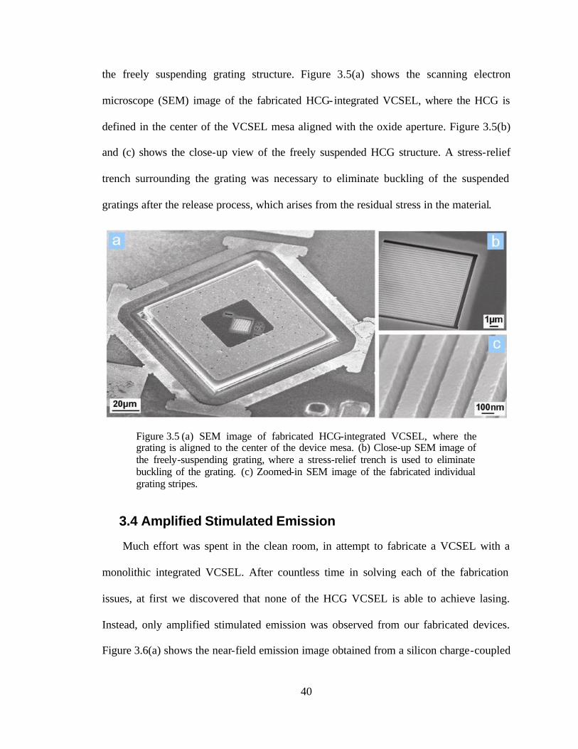
40
the freely suspending grating structure. Figure 3.5(a) shows the scanning electron
microscope (SEM) image of the fabricated HCG-integrated VCSEL, where the HCG is
defined in the center of the VCSEL mesa aligned with the oxide aperture. Figure 3.5(b)
and (c) shows the close-up view of the freely suspended HCG structure. A stress-relief
trench surrounding the grating was necessary to eliminate buckling of the suspended
gratings after the release process, which arises from the residual stress in the material.
Figure 3.5 (a) SEM image of fabricated HCG-integrated VCSEL, where the grating is aligned to the center of the device mesa. (b) Close-up SEM image of the freely-suspending grating, where a stress-relief trench is used to eliminate buckling of the grating. (c) Zoomed-in SEM image of the fabricated individual grating stripes.
3.4 Amplified Stimulated Emission
Much effort was spent in the clean room, in attempt to fabricate a VCSEL with a
monolithic integrated VCSEL. After countless time in solving each of the fabrication
issues, at first we discovered that none of the HCG VCSEL is able to achieve lasing.
Instead, only amplified stimulated emission was observed from our fabricated devices.
Figure 3.6(a) shows the near-field emission image obtained from a silicon charge-coupled
41
device (CCD) display. Not only was the intensity weaker, it lacks the signature patterns
of a typical laser – the interference speckles that can be seen from Figure 3.6(b).
(a) (b)
Figure 3.6 Near-field image obtain from a silicon CCD camera for (a) a not-lasing HCG VCSEL and (b) a lasing HCG VCSEL.
Figure 3.7 shows the measured emission spectrum for the HCG integrated VCSEL
device for both TM and TE polarizations. Two peaks were observed in the spectrum,
revealing the same 20-nm mismatch of the QW gain peak (blue side) and the VCSEL
cavity resonance mode (red side). For the TM polarization, the emission in the cavity
mode is enhanced by ~20 dB comparing to the gain peak due to the high reflectivity of
the SWG top mirror. In contrast, the emission for the TE polarization is dominated by the
gain peak of the active layer due to insufficient reflectivity from the SWG in this
polarization. To analyze the reflectivity of the fabricated SWG, a calculation was
performed based on the transmission matrix method. The reflectivity of the SWG is
estimated to be ~90% from calculating the emission spectrum of a half-cavity VCSEL
with an external broadband reflector.
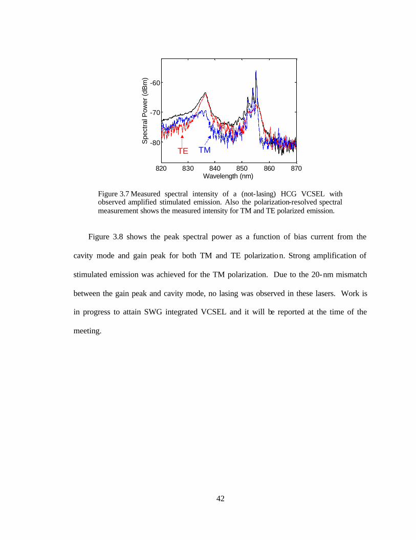
42
820 830 840 850 860 870
-80
-70
-60
Wavelength (nm)
Spe
ctra
l Pow
er (d
Bm
)TMTE
820 830 840 850 860 870
-80
-70
-60
Wavelength (nm)
Spe
ctra
l Pow
er (d
Bm
)TMTE
Figure 3.7 Measured spectral intensity of a (not-lasing) HCG VCSEL with observed amplified stimulated emission. Also the polarization-resolved spectral measurement shows the measured intensity for TM and TE polarized emission.
Figure 3.8 shows the peak spectral power as a function of bias current from the
cavity mode and gain peak for both TM and TE polarization. Strong amplification of
stimulated emission was achieved for the TM polarization. Due to the 20-nm mismatch
between the gain peak and cavity mode, no lasing was observed in these lasers. Work is
in progress to attain SWG integrated VCSEL and it will be reported at the time of the
meeting.
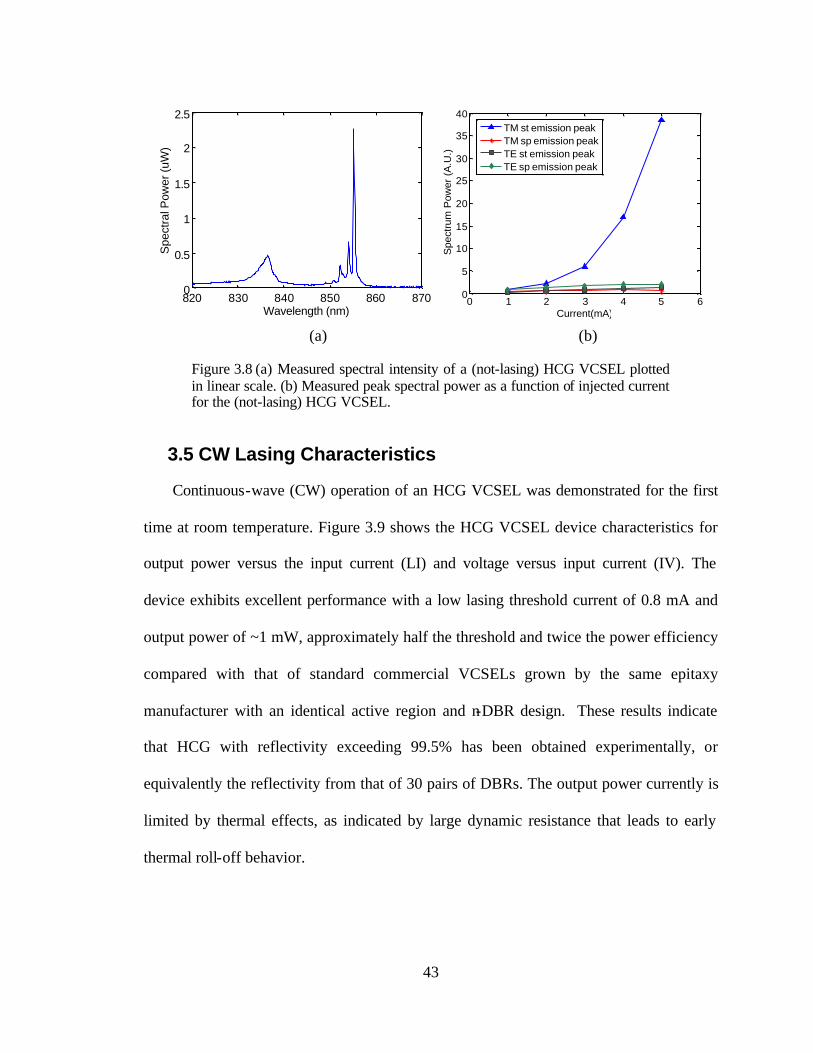
43
820 830 840 850 860 8700
0.5
1
1.5
2
2.5
Wavelength (nm)
Spe
ctra
l Pow
er (u
W)
0 1 2 3 4 5 60
5
10
15
20
25
30
35
40
Spe
ctru
m P
ower
(A
.U.)
Current(mA)
TM st emission peakTM sp emission peakTE st emission peakTE sp emission peak
(a) (b)
Figure 3.8 (a) Measured spectral intensity of a (not-lasing) HCG VCSEL plotted in linear scale. (b) Measured peak spectral power as a function of injected current for the (not-lasing) HCG VCSEL.
3.5 CW Lasing Characteristics
Continuous-wave (CW) operation of an HCG VCSEL was demonstrated for the first
time at room temperature. Figure 3.9 shows the HCG VCSEL device characteristics for
output power versus the input current (LI) and voltage versus input current (IV). The
device exhibits excellent performance with a low lasing threshold current of 0.8 mA and
output power of ~1 mW, approximately half the threshold and twice the power efficiency
compared with that of standard commercial VCSELs grown by the same epitaxy
manufacturer with an identical active region and n-DBR design. These results indicate
that HCG with reflectivity exceeding 99.5% has been obtained experimentally, or
equivalently the reflectivity from that of 30 pairs of DBRs. The output power currently is
limited by thermal effects, as indicated by large dynamic resistance that leads to early
thermal roll-off behavior.
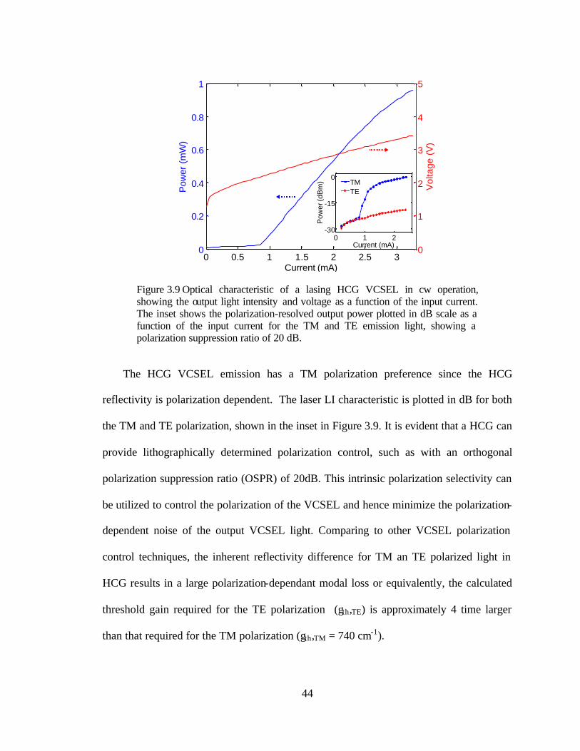
44
0 0.5 1 1.5 2 2.5 30
0.2
0.4
0.6
0.8
1
Current (mA)
Pow
er (
mW
)
0
1
2
3
4
5
Vol
tage
(V
)
0 1 2-30
-15
0
Current (mA)
Pow
er (d
Bm
) TMTE
Figure 3.9 Optical characteristic of a lasing HCG VCSEL in cw operation, showing the output light intensity and voltage as a function of the input current. The inset shows the polarization-resolved output power plotted in dB scale as a function of the input current for the TM and TE emission light, showing a polarization suppression ratio of 20 dB.
The HCG VCSEL emission has a TM polarization preference since the HCG
reflectivity is polarization dependent. The laser LI characteristic is plotted in dB for both
the TM and TE polarization, shown in the inset in Figure 3.9. It is evident that a HCG can
provide lithographically determined polarization control, such as with an orthogonal
polarization suppression ratio (OSPR) of 20dB. This intrinsic polarization selectivity can
be utilized to control the polarization of the VCSEL and hence minimize the polarization-
dependent noise of the output VCSEL light. Comparing to other VCSEL polarization
control techniques, the inherent reflectivity difference for TM an TE polarized light in
HCG results in a large polarization-dependant modal loss or equivalently, the calculated
threshold gain required for the TE polarization (gth,TE) is approximately 4 time larger
than that required for the TM polarization (gth,TM = 740 cm-1).
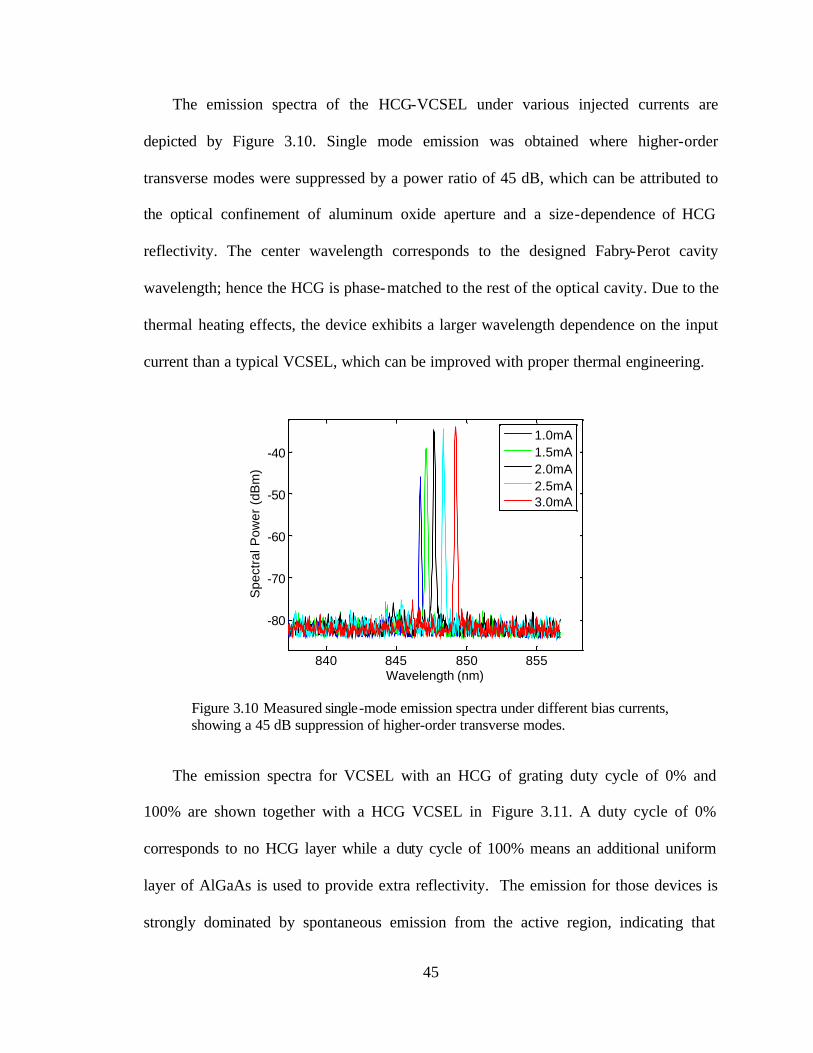
45
The emission spectra of the HCG-VCSEL under various injected currents are
depicted by Figure 3.10. Single mode emission was obtained where higher-order
transverse modes were suppressed by a power ratio of 45 dB, which can be attributed to
the optical confinement of aluminum oxide aperture and a size-dependence of HCG
reflectivity. The center wavelength corresponds to the designed Fabry-Perot cavity
wavelength; hence the HCG is phase-matched to the rest of the optical cavity. Due to the
thermal heating effects, the device exhibits a larger wavelength dependence on the input
current than a typical VCSEL, which can be improved with proper thermal engineering.
840 845 850 855
-80
-70
-60
-50
-40
Wavelength (nm)
Spe
ctra
l Pow
er (
dBm
)
1.0mA1.5mA2.0mA2.5mA3.0mA
Figure 3.10 Measured single-mode emission spectra under different bias currents, showing a 45 dB suppression of higher-order transverse modes.
The emission spectra for VCSEL with an HCG of grating duty cycle of 0% and
100% are shown together with a HCG VCSEL in Figure 3.11. A duty cycle of 0%
corresponds to no HCG layer while a duty cycle of 100% means an additional uniform
layer of AlGaAs is used to provide extra reflectivity. The emission for those devices is
strongly dominated by spontaneous emission from the active region, indicating that
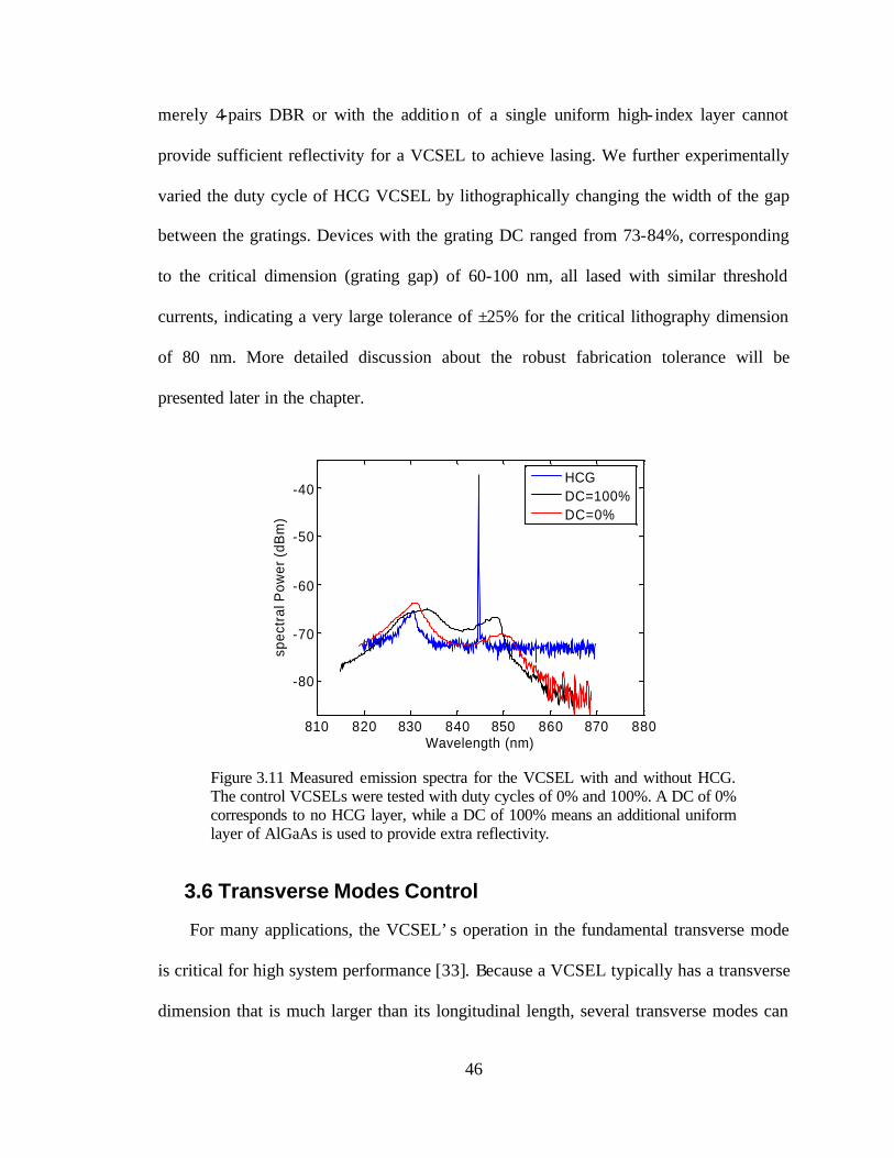
46
merely 4-pairs DBR or with the addition of a single uniform high- index layer cannot
provide sufficient reflectivity for a VCSEL to achieve lasing. We further experimentally
varied the duty cycle of HCG VCSEL by lithographically changing the width of the gap
between the gratings. Devices with the grating DC ranged from 73-84%, corresponding
to the critical dimension (grating gap) of 60-100 nm, all lased with similar threshold
currents, indicating a very large tolerance of ±25% for the critical lithography dimension
of 80 nm. More detailed discussion about the robust fabrication tolerance will be
presented later in the chapter.
810 820 830 840 850 860 870 880
-80
-70
-60
-50
-40
Wavelength (nm)
spec
tral
Pow
er (d
Bm
)
HCGDC=100%DC=0%
Figure 3.11 Measured emission spectra for the VCSEL with and without HCG. The control VCSELs were tested with duty cycles of 0% and 100%. A DC of 0% corresponds to no HCG layer, while a DC of 100% means an additional uniform layer of AlGaAs is used to provide extra reflectivity.
3.6 Transverse Modes Control
For many applications, the VCSEL’s operation in the fundamental transverse mode
is critical for high system performance [33]. Because a VCSEL typically has a transverse
dimension that is much larger than its longitudinal length, several transverse modes can
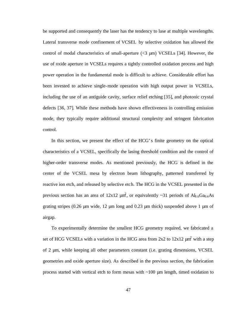
47
be supported and consequently the laser has the tendency to lase at multiple wavelengths.
Lateral transverse mode confinement of VCSEL by selective oxidation has allowed the
control of modal characteristics of small-aperture (<3 µm) VCSELs [34]. However, the
use of oxide aperture in VCSELs requires a tightly controlled oxidation process and high
power operation in the fundamental mode is difficult to achieve. Considerable effort has
been invested to achieve single-mode operation with high output power in VCSELs,
including the use of an antiguide cavity, surface relief etching [35], and photonic crystal
defects [36, 37]. While these methods have shown effectiveness in controlling emission
mode, they typically require additional structural complexity and stringent fabrication
control.
In this section, we present the effect of the HCG’s finite geometry on the optical
characteristics of a VCSEL, specifically the lasing threshold condition and the control of
higher-order transverse modes. As mentioned previously, the HCG is defined in the
center of the VCSEL mesa by electron beam lithography, patterned transferred by
reactive ion etch, and released by selective etch. The HCG in the VCSEL presented in the
previous section has an area of 12x12 µm2, or equivalently ~31 periods of Al0.6Ga0.4As
grating stripes (0.26 µm wide, 12 µm long and 0.23 µm thick) suspended above 1 µm of
airgap.
To experimentally determine the smallest HCG geometry required, we fabricated a
set of HCG VCSELs with a variation in the HCG area from 2x2 to 12x12 µm2 with a step
of 2 µm, while keeping all other parameters constant (i.e. grating dimensions, VCSEL
geometries and oxide aperture size). As described in the previous section, the fabrication
process started with vertical etch to form mesas with ~100 µm length, timed oxidation to
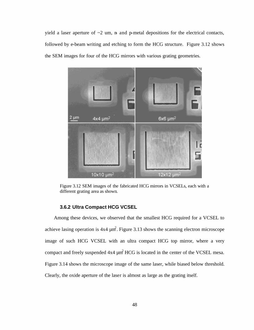
48
yield a laser aperture of ~2 um, n- and p-metal depositions for the electrical contacts,
followed by e-beam writing and etching to form the HCG structure. Figure 3.12 shows
the SEM images for four of the HCG mirrors with various grating geometries.
Figure 3.12 SEM images of the fabricated HCG mirrors in VCSELs, each with a different grating area as shown.
3.6.2 Ultra Compact HCG VCSEL
Among these devices, we observed that the smallest HCG required for a VCSEL to
achieve lasing operation is 4x4 µm2. Figure 3.13 shows the scanning electron microscope
image of such HCG VCSEL with an ultra compact HCG top mirror, where a very
compact and freely suspended 4x4 µm2 HCG is located in the center of the VCSEL mesa.
Figure 3.14 shows the microscope image of the same laser, while biased below threshold.
Clearly, the oxide aperture of the laser is almost as large as the grating itself.
49
(a) (b)
Figure 3.13 (a) SEM images of an ultra compact HCG VCSEL utilizing a 4x4 µm2 HCG as the top mirror. (b) SEM image of the freely suspended HCG, which consists of merely 11 Al0.6 Ga0.4As grating stripes with a thickness of 230 nm.
Figure 3.14 Microscope image of a HCG VCSEL with a compact 4x4 µm2 HCG top mirror , while biased below threshold.
Figure 3.15 shows the measured light intensity versus input electrical current (LI)
characteristic of such lasing device with the HCG area of 4x4 µm2, which corresponds to
merely 11 periods of subwavelength grating (370 nm period). Since the mesa size is
significantly larger than the oxide aperture, the alignment of HCG relative to the oxide
aperture has an estimated ~1 µm inaccuracy. Given the alignment inaccuracy, we
estimate equivalently only 3~5 periods for each direction from the beam center is
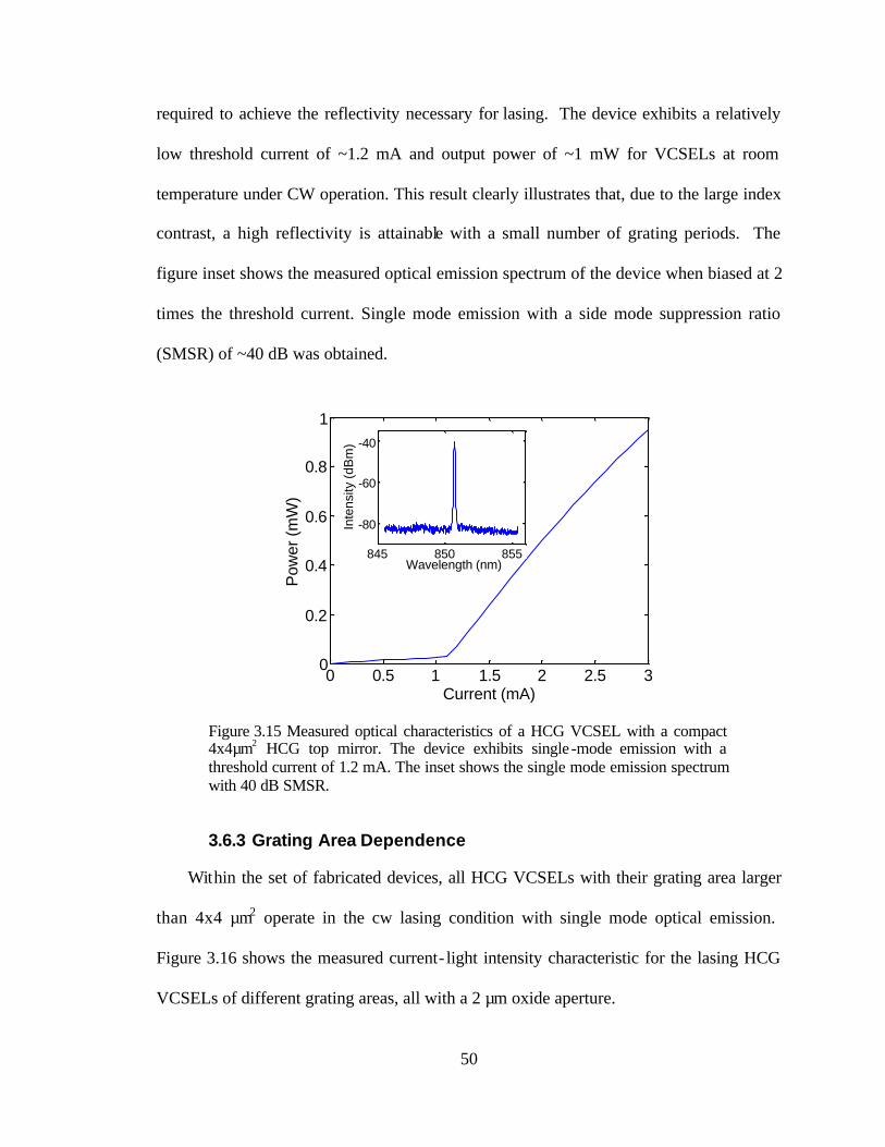
50
required to achieve the reflectivity necessary for lasing. The device exhibits a relatively
low threshold current of ~1.2 mA and output power of ~1 mW for VCSELs at room
temperature under CW operation. This result clearly illustrates that, due to the large index
contrast, a high reflectivity is attainable with a small number of grating periods. The
figure inset shows the measured optical emission spectrum of the device when biased at 2
times the threshold current. Single mode emission with a side mode suppression ratio
(SMSR) of ~40 dB was obtained.
0 0.5 1 1.5 2 2.5 30
0.2
0.4
0.6
0.8
1
Current (mA)
Pow
er (m
W)
850Wavelength (nm)
845 850 855
-80
-60
-40
Wavelength (nm)
Inte
nsity
(dB
m)
0 0.5 1 1.5 2 2.5 30
0.2
0.4
0.6
0.8
1
Current (mA)
Pow
er (m
W)
850Wavelength (nm)
845 850 855
-80
-60
-40
Wavelength (nm)
Inte
nsity
(dB
m)
Figure 3.15 Measured optical characteristics of a HCG VCSEL with a compact 4x4µm2 HCG top mirror. The device exhibits single -mode emission with a threshold current of 1.2 mA. The inset shows the single mode emission spectrum with 40 dB SMSR.
3.6.3 Grating Area Dependence
Within the set of fabricated devices, all HCG VCSELs with their grating area larger
than 4x4 µm2 operate in the cw lasing condition with single mode optical emission.
Figure 3.16 shows the measured current- light intensity characteristic for the lasing HCG
VCSELs of different grating areas, all with a 2 µm oxide aperture.
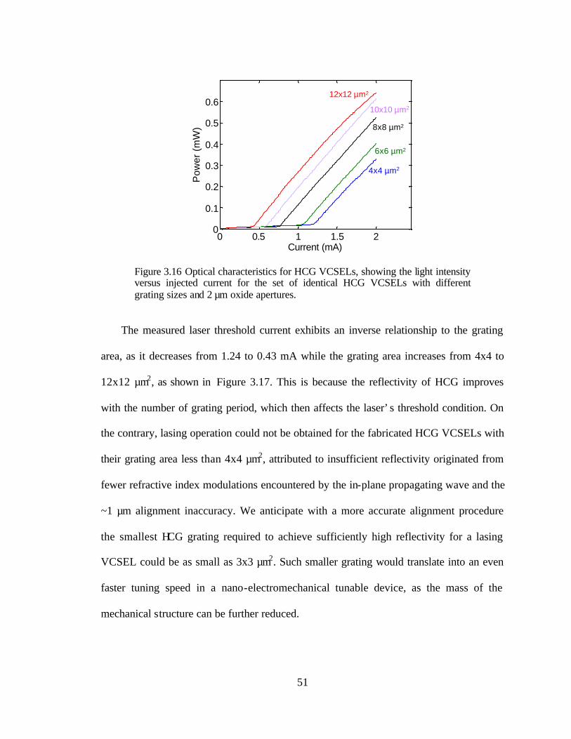
51
0 0.5 1 1.5 20
0.1
0.2
0.3
0.4
0.5
0.6
Current (mA)
Pow
er (
mW
)
4x4 µm2
6x6 µm2
8x8 µm2
10x10 µm2
12x12 µm2
0 0.5 1 1.5 20
0.1
0.2
0.3
0.4
0.5
0.6
Current (mA)
Pow
er (
mW
)
4x4 µm2
6x6 µm2
8x8 µm2
10x10 µm2
12x12 µm2
Figure 3.16 Optical characteristics for HCG VCSELs, showing the light intensity versus injected current for the set of identical HCG VCSELs with different grating sizes and 2 µm oxide apertures.
The measured laser threshold current exhibits an inverse relationship to the grating
area, as it decreases from 1.24 to 0.43 mA while the grating area increases from 4x4 to
12x12 µm2, as shown in Figure 3.17. This is because the reflectivity of HCG improves
with the number of grating period, which then affects the laser’s threshold condition. On
the contrary, lasing operation could not be obtained for the fabricated HCG VCSELs with
their grating area less than 4x4 µm2, attributed to insufficient reflectivity originated from
fewer refractive index modulations encountered by the in-plane propagating wave and the
~1 µm alignment inaccuracy. We anticipate with a more accurate alignment procedure
the smallest HCG grating required to achieve sufficiently high reflectivity for a lasing
VCSEL could be as small as 3x3 µm2. Such smaller grating would translate into an even
faster tuning speed in a nano-electromechanical tunable device, as the mass of the
mechanical structure can be further reduced.
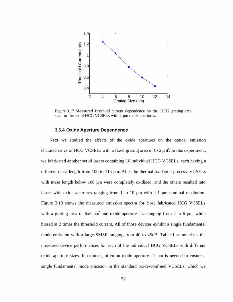
52
2 4 6 8 10 12 14
0.4
0.6
0.8
1
1.2
1.4
Grating Size (µm)
Thr
esho
ld C
urre
nt (m
A)
Figure 3.17 Measured threshold current dependence on the HCG grating area size for the set of HCG VCSELs with 2 µm oxide apertures.
3.6.4 Oxide Aperture Dependence
Next we studied the effects of the oxide apertures on the optical emission
characteristics of HCG VCSELs with a fixed grating area of 6x6 µm2. In this experiment,
we fabricated another set of lasers containing 16 individual HCG VCSELs, each having a
different mesa length from 100 to 115 µm. After the thermal oxidation process, VCSELs
with mesa length below 106 µm were completely oxidized, and the others resulted into
lasers with oxide apertures ranging from 1 to 10 µm with a 1 µm nominal resolution.
Figure 3.18 shows the measured emission spectra for those fabricated HCG VCSELs
with a grating area of 6x6 µm2 and oxide aperture size ranging from 2 to 6 µm, while
biased at 2 times the threshold current. All of those devices exhibit a single fundamental
mode emission with a large SMSR ranging from 40 to 45dB. Table 1 summarizes the
measured device performances for each of the individual HCG VCSELs with different
oxide aperture sizes. In contrast, often an oxide aperture =2 µm is needed to ensure a
single fundamental mode emission in the standard oxide-confined VCSELs, which we
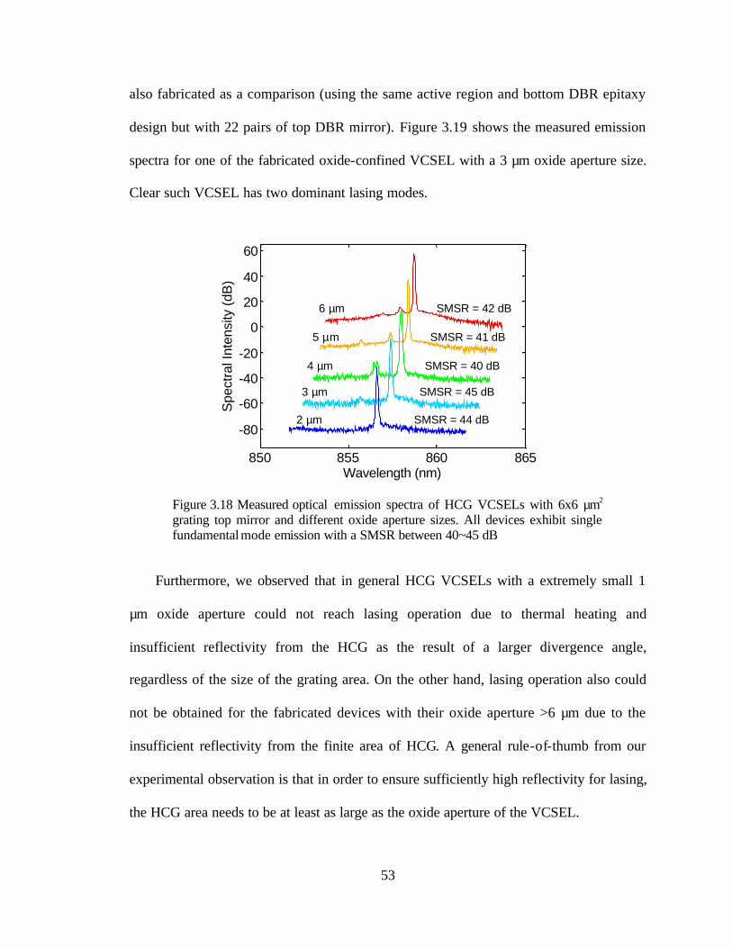
53
also fabricated as a comparison (using the same active region and bottom DBR epitaxy
design but with 22 pairs of top DBR mirror). Figure 3.19 shows the measured emission
spectra for one of the fabricated oxide-confined VCSEL with a 3 µm oxide aperture size.
Clear such VCSEL has two dominant lasing modes.
850 855 860 865
-80
-60
-40
-20
0
20
40
60
Wavelength (nm)
Spe
ctra
l Int
ensi
ty (d
B)
2 µm SMSR = 44 dB
3 µm SMSR = 45 dB
4 µm SMSR = 40 dB
5 µm SMSR = 41 dB
6 µm SMSR = 42 dB
850 855 860 865
-80
-60
-40
-20
0
20
40
60
Wavelength (nm)
Spe
ctra
l Int
ensi
ty (d
B)
2 µm SMSR = 44 dB
3 µm SMSR = 45 dB
4 µm SMSR = 40 dB
5 µm SMSR = 41 dB
6 µm SMSR = 42 dB
Figure 3.18 Measured optical emission spectra of HCG VCSELs with 6x6 µm2 grating top mirror and different oxide aperture sizes. All devices exhibit single fundamental mode emission with a SMSR between 40~45 dB
Furthermore, we observed that in general HCG VCSELs with a extremely small 1
µm oxide aperture could not reach lasing operation due to thermal heating and
insufficient reflectivity from the HCG as the result of a larger divergence angle,
regardless of the size of the grating area. On the other hand, lasing operation also could
not be obtained for the fabricated devices with their oxide aperture >6 µm due to the
insufficient reflectivity from the finite area of HCG. A general rule-of-thumb from our
experimental observation is that in order to ensure sufficiently high reflectivity for lasing,
the HCG area needs to be at least as large as the oxide aperture of the VCSEL.
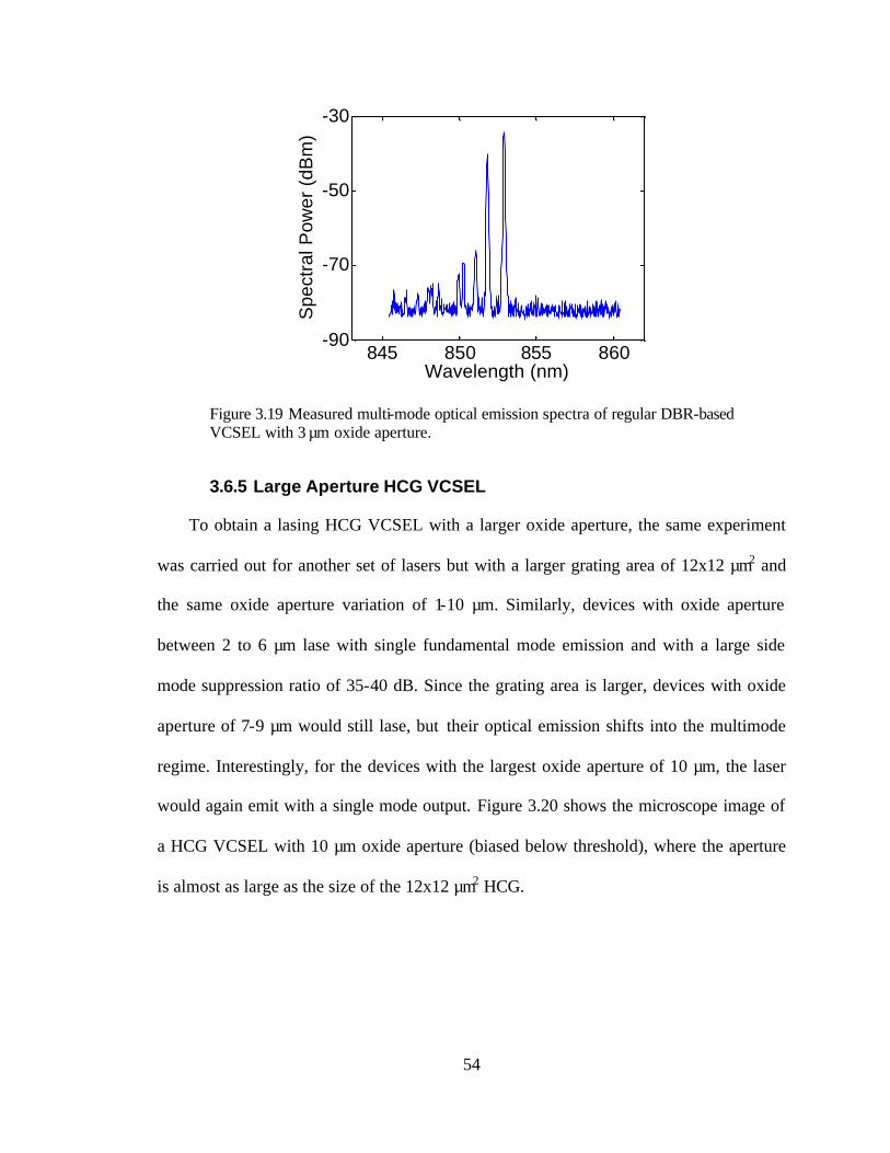
54
845 850 855 860-90
-70
-50
-30
Wavelength (nm)
Spe
ctra
l Pow
er (
dBm
)
Figure 3.19 Measured multi-mode optical emission spectra of regular DBR-based VCSEL with 3 µm oxide aperture.
3.6.5 Large Aperture HCG VCSEL
To obtain a lasing HCG VCSEL with a larger oxide aperture, the same experiment
was carried out for another set of lasers but with a larger grating area of 12x12 µm2 and
the same oxide aperture variation of 1-10 µm. Similarly, devices with oxide aperture
between 2 to 6 µm lase with single fundamental mode emission and with a large side
mode suppression ratio of 35-40 dB. Since the grating area is larger, devices with oxide
aperture of 7-9 µm would still lase, but their optical emission shifts into the multimode
regime. Interestingly, for the devices with the largest oxide aperture of 10 µm, the laser
would again emit with a single mode output. Figure 3.20 shows the microscope image of
a HCG VCSEL with 10 µm oxide aperture (biased below threshold), where the aperture
is almost as large as the size of the 12x12 µm2 HCG.
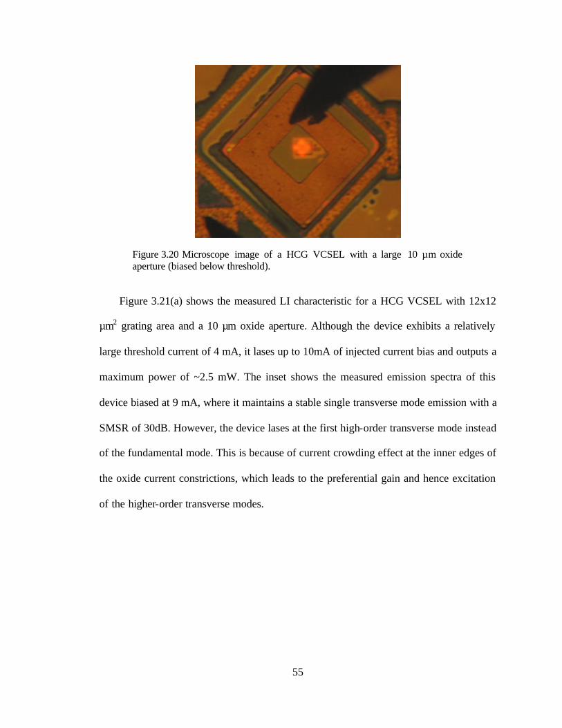
55
Figure 3.20 Microscope image of a HCG VCSEL with a large 10 µm oxide aperture (biased below threshold).
Figure 3.21(a) shows the measured LI characteristic for a HCG VCSEL with 12x12
µm2 grating area and a 10 µm oxide aperture. Although the device exhibits a relatively
large threshold current of 4 mA, it lases up to 10mA of injected current bias and outputs a
maximum power of ~2.5 mW. The inset shows the measured emission spectra of this
device biased at 9 mA, where it maintains a stable single transverse mode emission with a
SMSR of 30dB. However, the device lases at the first high-order transverse mode instead
of the fundamental mode. This is because of current crowding effect at the inner edges of
the oxide current constrictions, which leads to the preferential gain and hence excitation
of the higher-order transverse modes.
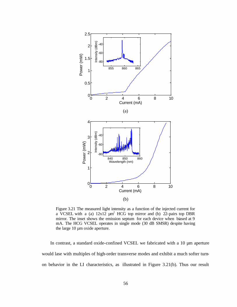
56
0 2 4 6 8 100
0.5
1
1.5
2
2.5
Current (mA)
Pow
er (
mW
)
855 860 865
-80
-60
-40
Inte
nsity
(dB
m)
0 2 4 6 8 100
0.5
1
1.5
2
2.5
Current (mA)
Pow
er (
mW
)
855 860 865
-80
-60
-40
Inte
nsity
(dB
m)
(a)
0 2 4 6 8 100
1
2
3
4
Current (mA)
Pow
er (
mW
)
840 850 860-80
-60
-40
Wavelength (nm)
Inte
nsity
(dB
m)
0 2 4 6 8 100
1
2
3
4
Current (mA)
Pow
er (
mW
)
840 850 860-80
-60
-40
Wavelength (nm)
Inte
nsity
(dB
m)
(b)
Figure 3.21 The measured light intensity as a function of the injected current for a VCSEL with a (a) 12x12 µm2 HCG top mirror and (b) 22-pairs top DBR mirror. The inset shows the emission septum for each device when biased at 9 mA. The HCG VCSEL operates in single mode (30 dB SMSR) despite having the large 10 µm oxide aperture.
In contrast, a standard oxide-confined VCSEL we fabricated with a 10 µm aperture
would lase with multiples of high-order transverse modes and exhibit a much softer turn-
on behavior in the LI characteristics, as illustrated in Figure 3.21(b). Thus our result
57
indicates that the control of high-order modes using a HCG is highly promising for
designing VCSELs for high power applications.
3.7 Polarization Mode Control
The applications of VCSELs have been significantly limited due to the lack of pre-
determined polarization control in conventional VCSELs using distributed Bragg
reflectors (DBRs) [33]. In essence, polarization mode represents a degenerate transverse
mode, which can cause mode partition noise even when minute, unintentional
polarization dependence exists in an optical link. Considerable effort has been invested to
achieve stable-polarization operation in VCSELs, including the use of anisotropic optical
gain in (311)B substrate [38] or anisotropic optical loss using shallow surface grating
etched onto the top DBR [39-41].
In this work, we present highly effective and deterministic polarization mode control
in HCG-VCSEL under both CW and pulsed operation. Figure 3.22 shows the SEM image
of a fabricated HCG VCSEL. With the flexibility given by e-beam lithography, we
fabricated several HCG VCSELs with their grating stripes oriented in different angles
with respect to the [011] crystal axis direction.
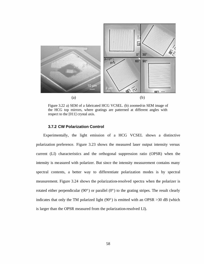
58
(a) (b)
Figure 3.22 a) SEM of a fabricated HCG VCSEL. (b) zoomed-in SEM image of the HCG top mirrors, where gratings are patterned at different angles with respect to the [011] crystal axis.
3.7.2 CW Polarization Control
Experimentally, the light emission of a HCG VCSEL shows a distinctive
polarization preference. Figure 3.23 shows the measured laser output intensity versus
current (LI) characteristics and the orthogonal suppression ratio (OPSR) when the
intensity is measured with polarizer. But since the intensity measurement contains many
spectral contents, a better way to differentiate polarization modes is by spectral
measurement. Figure 3.24 shows the polarization-resolved spectra when the polarizer is
rotated either perpendicular (90°) or parallel (0°) to the grating stripes. The result clearly
indicates that only the TM polarized light (90°) is emitted with an OPSR >30 dB (which
is larger than the OPSR measured from the polarization-resolved LI).
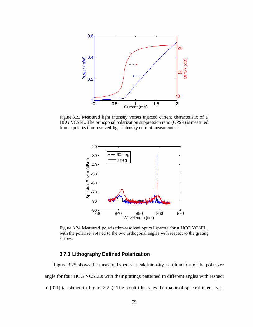
59
0 0.5 1 1.5 20
0.2
0.4
0.6
Current (mA)
Pow
er (m
W)
0 0.5 1 1.5 2
0
10
20
OP
SR
(dB
)
0 0.5 1 1.5 20
0.2
0.4
0.6
Current (mA)
Pow
er (m
W)
0 0.5 1 1.5 2
0
10
20
OP
SR
(dB
)
Figure 3.23 Measured light intensity versus injected current characteristic of a HCG VCSEL. The orthogonal polarization suppression ratio (OPSR) is measured from a polarization-resolved light intensity-current measurement.
830 840 850 860 870-90
-80
-70
-60
-50
-40
-30
-20
Wavelength (nm)
Spe
ctra
l Pow
er (d
Bm
)
90 deg0 deg
Figure 3.24 Measured polarization-resolved optical spectra for a HCG VCSEL, with the polarizer rotated to the two orthogonal angles with respect to the grating stripes.
3.7.3 Lithography Defined Polarization
Figure 3.25 shows the measured spectral peak intensity as a function of the polarizer
angle for four HCG VCSELs with their gratings patterned in different angles with respect
to [011] (as shown in Figure 3.22). The result illustrates the maximal spectral intensity is
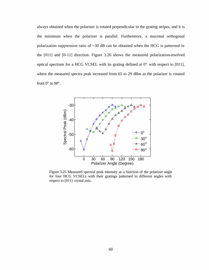
60
always obtained when the polarizer is rotated perpendicular to the grating stripes, and it is
the minimum when the polarizer is parallel. Furthermore, a maximal orthogonal
polarization suppression ratio of ~30 dB can be obtained when the HCG is patterned in
the [011] and [0-11] direction. Figure 3.26 shows the measured polarization-resolved
optical spectrum for a HCG VCSEL with its grating defined at 0° with respect to [011],
where the measured spectra peak increased from 65 to 29 dBm as the polarizer is rotated
from 0° to 90°.
0 30 60 90 120 150 180
-60
-50
-40
-30
Spe
ctra
l Pea
k (d
Bm
)
Polarizer Angle (Degree)
0o
30o
60o
90o
Figure 3.25 Measured spectral peak intensity as a function of the polarizer angle for four HCG VCSELs with their gratings patterned in different angles with respect to [011] crystal axis.
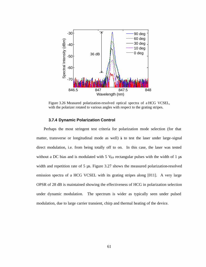
61
846.5 847 847.5 848
-70
-60
-50
-40
-30
Wavelength (nm)
Spe
ctra
l Int
ensi
ty (d
Bm
)
90 deg60 deg30 deg10 deg0 deg36 dB
846.5 847 847.5 848
-70
-60
-50
-40
-30
Wavelength (nm)
Spe
ctra
l Int
ensi
ty (d
Bm
)
90 deg60 deg30 deg10 deg0 deg36 dB
Figure 3.26 Measured polarization-resolved optical spectra of a HCG VCSEL, with the polarizer rotated to various angles with respect to the grating stripes.
3.7.4 Dynamic Polarization Control
Perhaps the most stringent test criteria for polarization mode selection (for that
matter, transverse or longitudinal mode as well) is to test the laser under large-signal
direct modulation, i.e. from being totally off to on. In this case, the laser was tested
without a DC bias and is modulated with 5 VPP rectangular pulses with the width of 1 µs
width and repetition rate of 5 µs. Figure 3.27 shows the measured polarization-resolved
emission spectra of a HCG VCSEL with its grating stripes along [011]. A very large
OPSR of 28 dB is maintained showing the effectiveness of HCG in polarization selection
under dynamic modulation. The spectrum is wider as typically seen under pulsed
modulation, due to large carrier transient, chirp and thermal heating of the device.
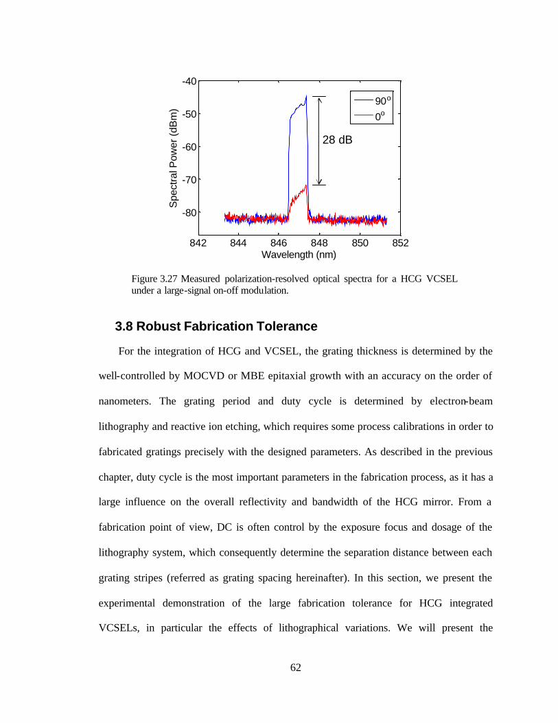
62
842 844 846 848 850 852
-80
-70
-60
-50
-40
Wavelength (nm)
Spe
ctra
l Pow
er (d
Bm
)
90o
0o
28 dB
842 844 846 848 850 852
-80
-70
-60
-50
-40
Wavelength (nm)
Spe
ctra
l Pow
er (d
Bm
)
90o
0o
28 dB
Figure 3.27 Measured polarization-resolved optical spectra for a HCG VCSEL under a large-signal on-off modulation.
3.8 Robust Fabrication Tolerance
For the integration of HCG and VCSEL, the grating thickness is determined by the
well-controlled by MOCVD or MBE epitaxial growth with an accuracy on the order of
nanometers. The grating period and duty cycle is determined by electron-beam
lithography and reactive ion etching, which requires some process calibrations in order to
fabricated gratings precisely with the designed parameters. As described in the previous
chapter, duty cycle is the most important parameters in the fabrication process, as it has a
large influence on the overall reflectivity and bandwidth of the HCG mirror. From a
fabrication point of view, DC is often control by the exposure focus and dosage of the
lithography system, which consequently determine the separation distance between each
grating stripes (referred as grating spacing hereinafter). In this section, we present the
experimental demonstration of the large fabrication tolerance for HCG integrated
VCSELs, in particular the effects of lithographical variations. We will present the
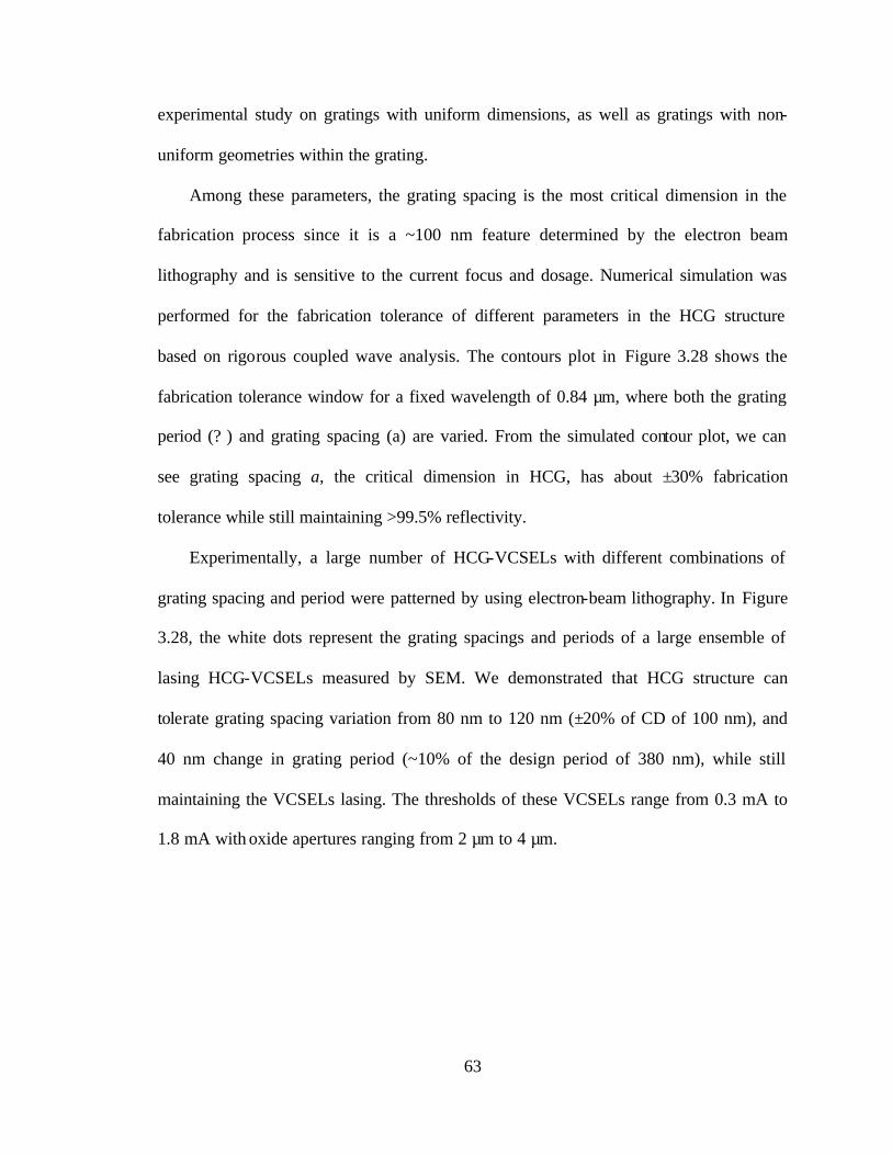
63
experimental study on gratings with uniform dimensions, as well as gratings with non-
uniform geometries within the grating.
Among these parameters, the grating spacing is the most critical dimension in the
fabrication process since it is a ~100 nm feature determined by the electron beam
lithography and is sensitive to the current focus and dosage. Numerical simulation was
performed for the fabrication tolerance of different parameters in the HCG structure
based on rigorous coupled wave analysis. The contours plot in Figure 3.28 shows the
fabrication tolerance window for a fixed wavelength of 0.84 µm, where both the grating
period (? ) and grating spacing (a) are varied. From the simulated contour plot, we can
see grating spacing a, the critical dimension in HCG, has about ±30% fabrication
tolerance while still maintaining >99.5% reflectivity.
Experimentally, a large number of HCG-VCSELs with different combinations of
grating spacing and period were patterned by using electron-beam lithography. In Figure
3.28, the white dots represent the grating spacings and periods of a large ensemble of
lasing HCG-VCSELs measured by SEM. We demonstrated that HCG structure can
tolerate grating spacing variation from 80 nm to 120 nm (±20% of CD of 100 nm), and
40 nm change in grating period (~10% of the design period of 380 nm), while still
maintaining the VCSELs lasing. The thresholds of these VCSELs range from 0.3 mA to
1.8 mA with oxide apertures ranging from 2 µm to 4 µm.
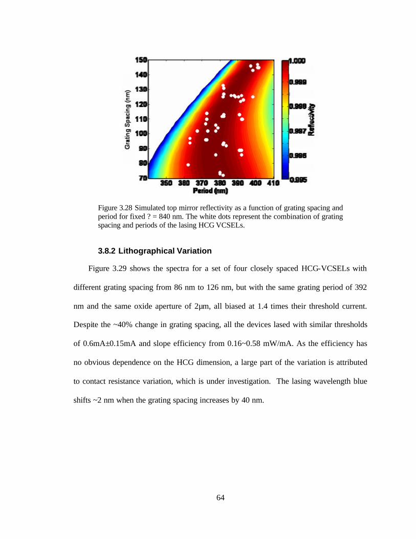
64
Figure 3.28 Simulated top mirror reflectivity as a function of grating spacing and period for fixed ? = 840 nm. The white dots represent the combination of grating spacing and periods of the lasing HCG VCSELs.
3.8.2 Lithographical Variation
Figure 3.29 shows the spectra for a set of four closely spaced HCG-VCSELs with
different grating spacing from 86 nm to 126 nm, but with the same grating period of 392
nm and the same oxide aperture of 2µm, all biased at 1.4 times their threshold current.
Despite the ~40% change in grating spacing, all the devices lased with similar thresholds
of 0.6mA±0.15mA and slope efficiency from 0.16~0.58 mW/mA. As the efficiency has
no obvious dependence on the HCG dimension, a large part of the variation is attributed
to contact resistance variation, which is under investigation. The lasing wavelength blue
shifts ~2 nm when the grating spacing increases by 40 nm.
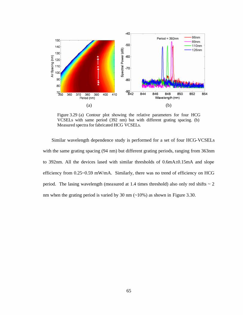
65
(a) (b)
Figure 3.29 (a) Contour plot showing the relative parameters for four HCG VCSELs with same period (392 nm) but with different grating spacing. (b) Measured spectra for fabricated HCG VCSELs.
Similar wavelength dependence study is performed for a set of four HCG-VCSELs
with the same grating spacing (94 nm) but different grating periods, ranging from 363nm
to 392nm. All the devices lased with similar thresholds of 0.6mA±0.15mA and slope
efficiency from 0.25~0.59 mW/mA. Similarly, there was no trend of efficiency on HCG
period. The lasing wavelength (measured at 1.4 times threshold) also only red shifts ~ 2
nm when the grating period is varied by 30 nm (~10%) as shown in Figure 3.30.
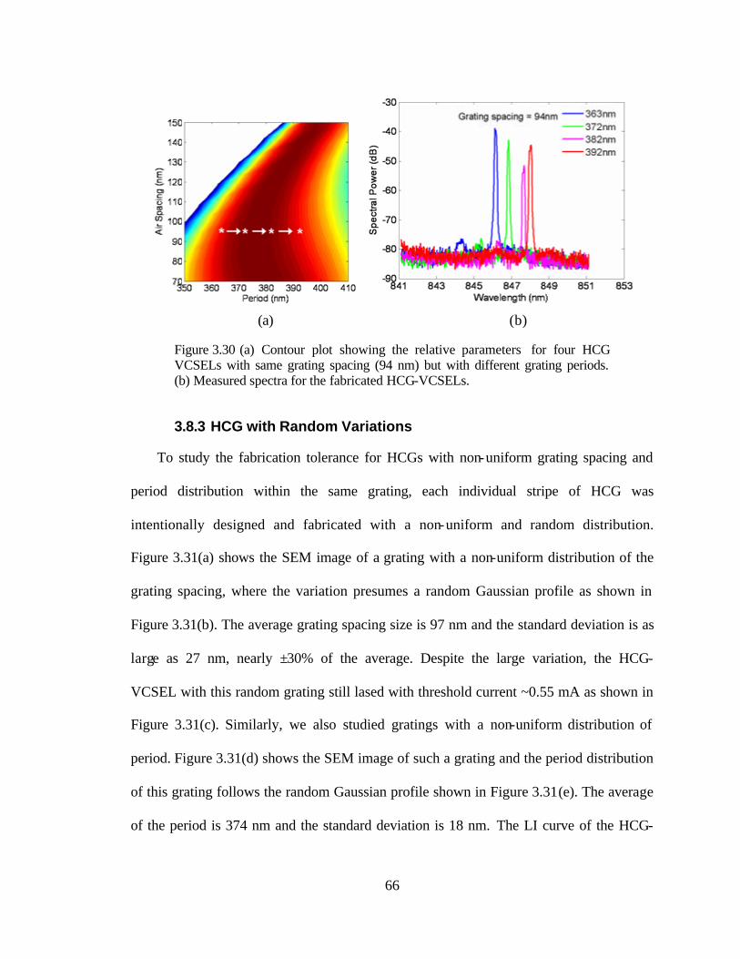
66
(a) (b)
Figure 3.30 (a) Contour plot showing the relative parameters for four HCG VCSELs with same grating spacing (94 nm) but with different grating periods. (b) Measured spectra for the fabricated HCG-VCSELs.
3.8.3 HCG with Random Variations
To study the fabrication tolerance for HCGs with non-uniform grating spacing and
period distribution within the same grating, each individual stripe of HCG was
intentionally designed and fabricated with a non-uniform and random distribution.
Figure 3.31(a) shows the SEM image of a grating with a non-uniform distribution of the
grating spacing, where the variation presumes a random Gaussian profile as shown in
Figure 3.31(b). The average grating spacing size is 97 nm and the standard deviation is as
large as 27 nm, nearly ±30% of the average. Despite the large variation, the HCG-
VCSEL with this random grating still lased with threshold current ~0.55 mA as shown in
Figure 3.31(c). Similarly, we also studied gratings with a non-uniform distribution of
period. Figure 3.31(d) shows the SEM image of such a grating and the period distribution
of this grating follows the random Gaussian profile shown in Figure 3.31(e). The average
of the period is 374 nm and the standard deviation is 18 nm. The LI curve of the HCG-
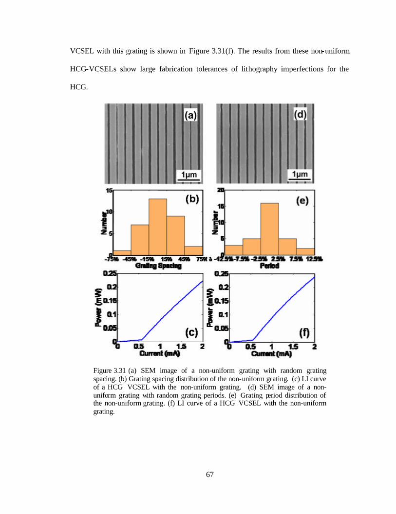
67
VCSEL with this grating is shown in Figure 3.31(f). The results from these non-uniform
HCG-VCSELs show large fabrication tolerances of lithography imperfections for the
HCG.
Figure 3.31 (a) SEM image of a non-uniform grating with random grating spacing. (b) Grating spacing distribution of the non-uniform grating. (c) LI curve of a HCG VCSEL with the non-uniform grating. (d) SEM image of a non-uniform grating with random grating periods. (e) Grating period distribution of the non-uniform grating. (f) LI curve of a HCG VCSEL with the non-uniform grating.
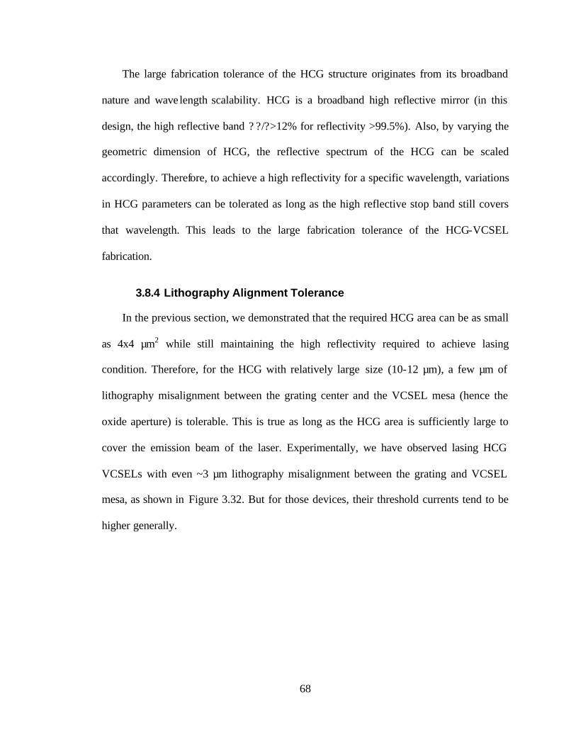
68
The large fabrication tolerance of the HCG structure originates from its broadband
nature and wavelength scalability. HCG is a broadband high reflective mirror (in this
design, the high reflective band ? ?/?>12% for reflectivity >99.5%). Also, by varying the
geometric dimension of HCG, the reflective spectrum of the HCG can be scaled
accordingly. Therefore, to achieve a high reflectivity for a specific wavelength, variations
in HCG parameters can be tolerated as long as the high reflective stop band still covers
that wavelength. This leads to the large fabrication tolerance of the HCG-VCSEL
fabrication.
3.8.4 Lithography Alignment Tolerance
In the previous section, we demonstrated that the required HCG area can be as small
as 4x4 µm2 while still maintaining the high reflectivity required to achieve lasing
condition. Therefore, for the HCG with relatively large size (10-12 µm), a few µm of
lithography misalignment between the grating center and the VCSEL mesa (hence the
oxide aperture) is tolerable. This is true as long as the HCG area is sufficiently large to
cover the emission beam of the laser. Experimentally, we have observed lasing HCG
VCSELs with even ~3 µm lithography misalignment between the grating and VCSEL
mesa, as shown in Figure 3.32. But for those devices, their threshold currents tend to be
higher generally.
69
Figure 3.32 SEM image of a fabricated HCG VCSEL with a 3 µm misalignment between the grating and VCSEL mesa (oxide aperture).
3.9 Summary
We demonstrate a VCSEL utilizing an integrated single- layer high- index-contrast
subwavelength grating as its top mirror, with air and AlGaAs as the low and high index
material, respectively. Without the conventional 20-25 pairs of top DBR, the fabricated
HCG VCSEL exhibits low threshold current, deterministic polarization, and single
transverse mode. We also show a theoretical guideline for the index contrast in HCG,
which opens up various material combination possibilities. For instance, a low-index
dielectric such as SiO 2 or Al2O3 can be used instead of air as the low-index material
underneath the grating.
We have shown that that merely 11 AlGaAs grating stripes with a thickness of 230
nm is sufficient to provide >99.5% reflectivity required for VCSEL to lase. Since the
high reflectivity is restricted within its patterned area, HCG can effectively discriminate
the higher-order transverse modes for oxide-VCSELs with up to 6 µm aperture with a
large side-mode suppression ratio >40 dB. Furthermore a single mode, high output power
70
of ~2.5 mW was experimentally demonstrated using a HCG VCSEL with a 10 µm oxide
aperture.
Besides providing high reflectivity, the utilization of a HCG can control the emission
polarization that is lithographically determined, such as with an orthogonal polarization
suppression ratio of ~30dB. This intrinsic polarization selectivity can be utilized to
control the polarization of the VCSEL and hence minimize the polarization-dependent
noise of VCSEL-based optical links.
Lastly, we experimentally demonstrated a very large fabrication tolerance for high
contrast subwavelength grating: ±20% critical dimension variation for a uniform HCG
and ±30% critical dimension va riation for a random size HCG. The VCSEL emission
wavelength is insensitive to the lithographical variations of HCG, which makes it
especially attractive for designing and manufacturing VCSELs for a fixed and desirable
wavelength for particular applications. These results show that a low-cost and high-
throughput fabrication process such as nano- imprinting [32] can be implemented for
large volume batch processing.
In short, the simplicity, wavelength-scalability, and versatility of the single- layer
HCG design would provide numerous benefits when fabricating surface-normal
optoelectronic devices such as VCSELs, high brightness LEDs, photo-voltaic cells,
optical filters and detectors, and micro-electromechanical (MEM) tunable devices, fo r a
wide range of wavelengths.
71
Chapter 4 Nano Electromechanical Tunable VCSEL
4.1 Motivation
The ability to tune the frequency of an oscillator is of critical importance and is a
fundamental building block for many systems, be they mechanical or electronic.
However, this very important function is still highly inadequate for optical oscillators,
particularly for semiconductor diode lasers [14, 15]. The inadequacies of tuning a laser
frequency (wavelength) include the tuning range and speed, which is typically
milliseconds or slower. In addition, the tuning is often not continuous and may require
complex synchronization of several electrical control signals.
A wavelength-tunable semiconductor laser has been constructed by combining an
optical micro-electromechanical (MEM) mirror with a vertical-cavity surface-emitting
laser (VCSEL) [16-19].The monolithic integration brings together the best of both
technologies and leads to an unprecedented performance in wavelength tunable lasers
with simple electrical control. The MEM tunable VCSEL has the majority part of its top
72
mirror being held on a micromechanical structure and is physically moved via
electrostatic attraction. The physical movement changes the optical cavity length and
thus produces a change in the lasing wavelength. The lasers have two pairs of electric
contacts, one for tuning the wavelength and the other for data modulation, which can be
at ~10 Gb/s data rates. In addition, the MEM tunable VCSELs offer advantages of batch
processing and wafer- level testing, which are essential for low-cost volume
manufacturability. But because of the short gain medium, VCSELs often require
distributed Bragg reflectors (DBRs) with a thickness of 3~6 times optical wavelength in
air to construct mirrors with sufficiently high reflectivity. This could be as thick as 4 µm
and 10 µm for VCSELs emitting at 850 nm and 1.55 µm wavelength, respectively. When
integrating with MEM structures, these rather thick DBRs impose significant design
limitations on the length and width of the MEM structures. Thus, the mass of the
movable structures translates into a slow tuning speed, a limited tuning range, high
actuation power, as well as epitaxy and processing difficulties.
In the previous chapter, we demonstrated the realization of a surface emitting laser
using an ultra-thin (230 nm) high-contrast subwavelength grating (HCG) reflector that
replaces the requirement for 30-40 pairs of DBRs in VCSELs. Experimentally the device
exhibits excellent optical performance such as low threshold current, moderate output
power, deterministic polarization and single mode emission [42]. The HCG structure
consists of a single layer of periodic subwavelength grating comprised of a high
refractive index material (e.g. AlGaAs or Si) surrounded entirely by low index material
(e.g. air or oxide) [27]. In this chapter, we present realization of a high-speed nano-
electromechanical optoelectronic (NEMO) tunable VCSEL by integrating the lightweight
73
HCG with nano-electromechanical actuators to create a mobile reflector. As such, the
small footprint of HCG enables the scaling down of the mechanical actuating structure by
at least a factor of 10 in each of the dimensions, and thus the overall mass is less than one
thousandth of regular DBR-based photonic MEMS devices, resulting in much smaller
power consumption and much faster tuning speed [43]. This allows for a wavelength-
tunable light source with potentially tens of nanoseconds switching speed and suggests
various new areas of practical applications such as bio- or chemical sensing [44-46],
chip-scale atomic clocks [47, 48], and projection displays [49, 50].
4.2 NEMO Design
The device schematic and cross-section of the electrostatic actuated NEMO tunable
VCSEL is shown in Figure 4.1. The device consists of an n-doped HCG top mirror, a
cavity layer containing the active region, and a bottom standard n-doped DBR mirror on
a GaAs substrate. The HCG is freely suspended above a variable airgap and supported
via a nano-mechanical structure (i.e. cantilever, bridge, folded beam, or membrane).
Electric current injection is conducted through the middle laser contact (via 2 pairs of p-
doped DBRs above the cavity layer) and backside contact (via substrate). An aluminum
oxide aperture is formed on an AlAs layer within the p-DBR section to provide current
and optical confinement. The mechanical tuning contact is fabricated on the top n-doped
HCG layer.
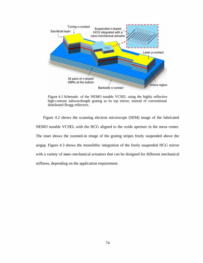
74
Figure 4.1 Schematic of the NEMO tunable VCSEL using the highly reflective high-contrast subwavelength grating as its top mirror, instead of conventional distributed Bragg reflectors.
Figure 4.2 shows the scanning electron microscope (SEM) image of the fabricated
NEMO tunable VCSEL with the HCG aligned to the oxide aperture in the mesa center.
The inset shows the zoomed-in image of the grating stripes freely suspended above the
airgap. Figure 4.3 shows the monolithic integration of the freely suspended HCG mirror
with a variety of nano-mechanical actuators that can be designed for different mechanical
stiffness, depending on the application requirement.
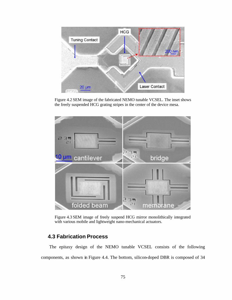
75
Figure 4.2 SEM image of the fabricated NEMO tunable VCSEL. The inset shows the freely suspended HCG grating stripes in the center of the device mesa.
Figure 4.3 SEM image of freely suspend HCG mirror monolithically integrated with various mobile and lightweight nano-mechanical actuators.
4.3 Fabrication Process
The epitaxy design of the NEMO tunable VCSEL consists of the following
components, as shown in Figure 4.4. The bottom, silicon-doped DBR is composed of 34
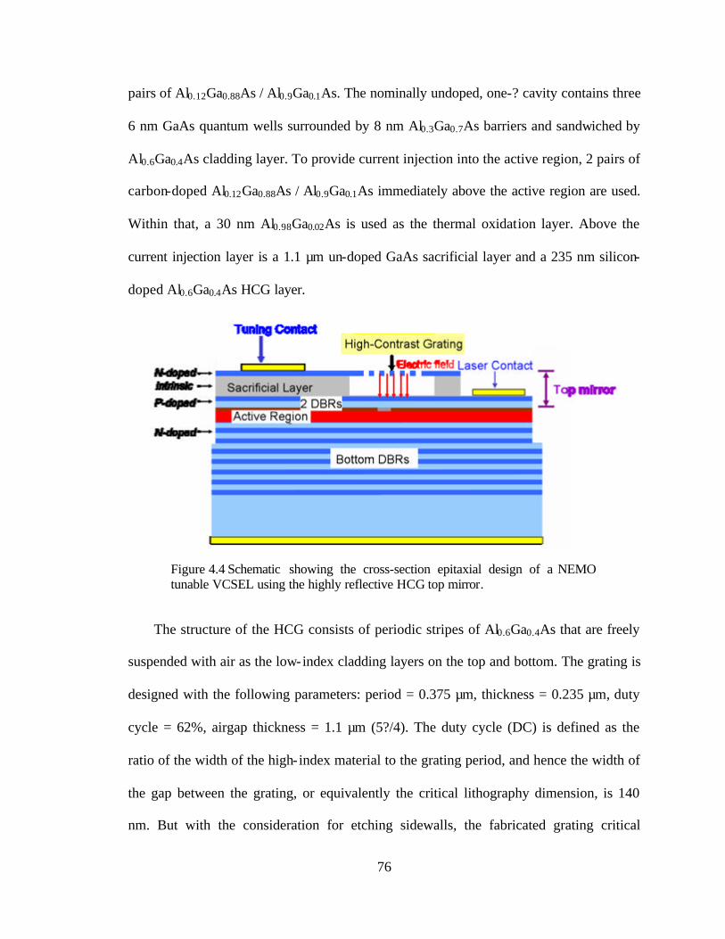
76
pairs of Al0.12Ga0.88As / Al0.9Ga0.1As. The nominally undoped, one-? cavity contains three
6 nm GaAs quantum wells surrounded by 8 nm Al0.3Ga0.7As barriers and sandwiched by
Al0.6Ga0.4As cladding layer. To provide current injection into the active region, 2 pairs of
carbon-doped Al0.12Ga0.88As / Al0.9Ga0.1As immediately above the active region are used.
Within that, a 30 nm Al0.98Ga0.02As is used as the thermal oxidation layer. Above the
current injection layer is a 1.1 µm un-doped GaAs sacrificial layer and a 235 nm silicon-
doped Al0.6Ga0.4As HCG layer.
Figure 4.4 Schematic showing the cross-section epitaxial design of a NEMO tunable VCSEL using the highly reflective HCG top mirror.
The structure of the HCG consists of periodic stripes of Al0.6Ga0.4As that are freely
suspended with air as the low-index cladding layers on the top and bottom. The grating is
designed with the following parameters: period = 0.375 µm, thickness = 0.235 µm, duty
cycle = 62%, airgap thickness = 1.1 µm (5?/4). The duty cycle (DC) is defined as the
ratio of the width of the high- index material to the grating period, and hence the width of
the gap between the grating, or equivalently the critical lithography dimension, is 140
nm. But with the consideration for etching sidewalls, the fabricated grating critical
77
dimension is slightly smaller (~100 nm). Similar to our prior work, the HCG has an area
of 12x12 µm2, or equivalently 31 periods of Al0.6Ga0.4As grating stripes (0.26 µm wide,
12 µm long and 0.23 µm thick) suspended above the 1.1 µm airgap.
The fabrication process of a nano-electromechanical tunable VCSEL is summarized
in Figure 4.5. The process starts with the mesa formation (~100 µm) by etching down to
the bottom DBRs and follows by the thermal oxidation to form the oxide aperture (~3
µm). Next steps are the top and back-side contact metal depositions, by using electron-
beam evaporator to deposit Ni-Ge-Au metal alloy. Then, part of the mesa surface is
etched to expose the p-doped current injection layer, on top of which the laser contact
metal (Ti-Au) is deposited. Lastly, the HCG is patterned by electron-beam lithography on
poly-methyl methacrylate (PMMA) photoresist and pattern transferred by reactive ion
etching, where the HCG is aligned to the mesa center (oxide aperture). A citric acid
based selective etch followed by critical point drying is required to remove the sacrificial
material underneath the HCG layer and form the freely suspended grating structure that is
supported by nano-mechanical beams.
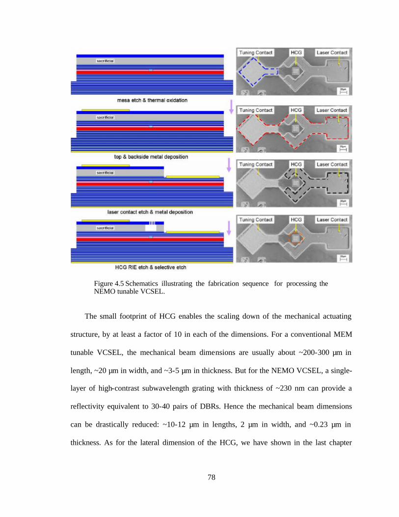
78
Figure 4.5 Schematics illustrating the fabrication sequence for processing the NEMO tunable VCSEL.
The small footprint of HCG enables the scaling down of the mechanical actuating
structure, by at least a factor of 10 in each of the dimensions. For a conventional MEM
tunable VCSEL, the mechanical beam dimensions are usually about ~200-300 µm in
length, ~20 µm in width, and ~3-5 µm in thickness. But for the NEMO VCSEL, a single-
layer of high-contrast subwavelength grating with thickness of ~230 nm can provide a
reflectivity equivalent to 30-40 pairs of DBRs. Hence the mechanical beam dimensions
can be drastically reduced: ~10-12 µm in lengths, 2 µm in width, and ~0.23 µm in
thickness. As for the lateral dimension of the HCG, we have shown in the last chapter
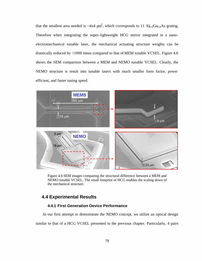
79
that the smallest area needed is ~4x4 µm2, which corresponds to 11 Al0.6Ga0.4As grating.
Therefore when integrating the super- lightweight HCG mirror integrated in a nano-
electromechanical tunable laser, the mechanical actuating structure weights can be
drastically reduced by >1000 times compared to that of MEM tunable VCSEL. Figure 4.6
shows the SEM comparison between a MEM and NEMO tunable VCSEL. Clearly, the
NEMO structure is result into tunable lasers with much smaller form factor, power
efficient, and faster tuning speed.
Figure 4.6 SEM images comparing the structural difference between a MEM and NEMO tunable VCSEL. The small footprint of HCG enables the scaling down of the mechanical structure.
4.4 Experimental Results
4.4.1 First Generation Device Performance
In our first attempt to demonstrate the NEMO concept, we utilize an optical design
similar to that of a HCG VCSEL presented in the previous chapter. Particularly, 4 pairs
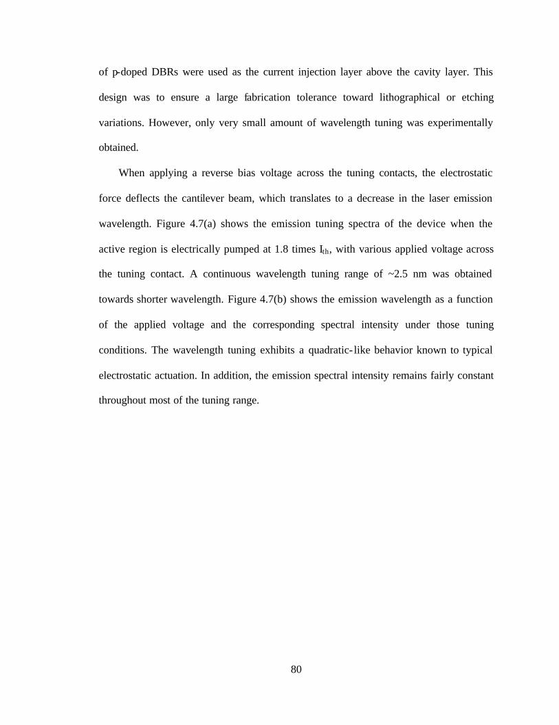
80
of p-doped DBRs were used as the current injection layer above the cavity layer. This
design was to ensure a large fabrication tolerance toward lithographical or etching
variations. However, only very small amount of wavelength tuning was experimentally
obtained.
When applying a reverse bias voltage across the tuning contacts, the electrostatic
force deflects the cantilever beam, which translates to a decrease in the laser emission
wavelength. Figure 4.7(a) shows the emission tuning spectra of the device when the
active region is electrically pumped at 1.8 times Ith, with various applied voltage across
the tuning contact. A continuous wavelength tuning range of ~2.5 nm was obtained
towards shorter wavelength. Figure 4.7(b) shows the emission wavelength as a function
of the applied voltage and the corresponding spectral intensity under those tuning
conditions. The wavelength tuning exhibits a quadratic- like behavior known to typical
electrostatic actuation. In addition, the emission spectral intensity remains fairly constant
throughout most of the tuning range.
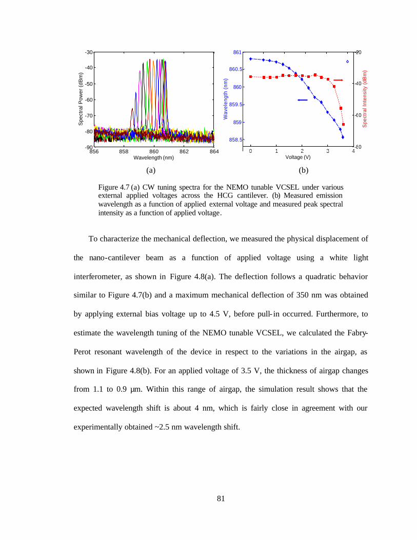
81
856 858 860 862 864-90
-80
-70
-60
-50
-40
-30
Wavelength (nm)
Spe
ctra
l Pow
er (
dBm
)
0 1 2 3 4
858.5
859
859.5
860
860.5
861
Voltage (V)
Wav
elen
gth
(nm
)
-80
-60
-40
-20
Spe
ctra
l Int
ensi
ty (
dBm
)
(a) (b)
Figure 4.7 (a) CW tuning spectra for the NEMO tunable VCSEL under various external applied voltages across the HCG cantilever. (b) Measured emission wavelength as a function of applied external voltage and measured peak spectral intensity as a function of applied voltage.
To characterize the mechanical deflection, we measured the physical displacement of
the nano-cantilever beam as a function of applied voltage using a white light
interferometer, as shown in Figure 4.8(a). The deflection follows a quadratic behavior
similar to Figure 4.7(b) and a maximum mechanical deflection of 350 nm was obtained
by applying external bias voltage up to 4.5 V, before pull- in occurred. Furthermore, to
estimate the wavelength tuning of the NEMO tunable VCSEL, we calculated the Fabry-
Perot resonant wavelength of the device in respect to the variations in the airgap, as
shown in Figure 4.8(b). For an applied voltage of 3.5 V, the thickness of airgap changes
from 1.1 to 0.9 µm. Within this range of airgap, the simulation result shows that the
expected wavelength shift is about 4 nm, which is fairly close in agreement with our
experimentally obtained ~2.5 nm wavelength shift.
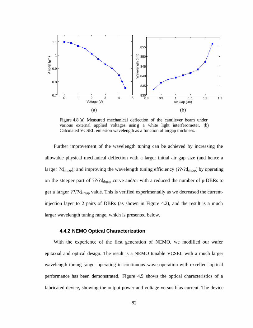
82
0 1 2 3 4 50.7
0.8
0.9
1
1.1
Voltage (V)
Airg
ap ( µ
m)
0.8 0.9 1 1.1 1.2 1.3830
835
840
845
850
855
Air Gap (µm)
Wav
elen
gth
(nm
)
(a) (b)
Figure 4.8 (a) Measured mechanical deflection of the cantilever beam under various external applied voltages using a white light interferometer. (b) Calculated VCSEL emission wavelength as a function of airgap thickness.
Further improvement of the wavelength tuning can be achieved by increasing the
allowable physical mechanical deflection with a larger initial air gap size (and hence a
larger ?dairgap); and improving the wavelength tuning efficiency (??/?dairgap) by operating
on the steeper part of ??/?dairgap curve and/or with a reduced the number of p-DBRs to
get a larger ??/?dairgap value. This is verified experimentally as we decreased the current-
injection layer to 2 pairs of DBRs (as shown in Figure 4.2), and the result is a much
larger wavelength tuning range, which is presented below.
4.4.2 NEMO Optical Characterization
With the experience of the first generation of NEMO, we modified our wafer
epitaxial and optical design. The result is a NEMO tunable VCSEL with a much larger
wavelength tuning range, operating in continuous-wave operation with excellent optical
performance has been demonstrated. Figure 4.9 shows the optical characteristics of a
fabricated device, showing the output power and voltage versus bias current. The device
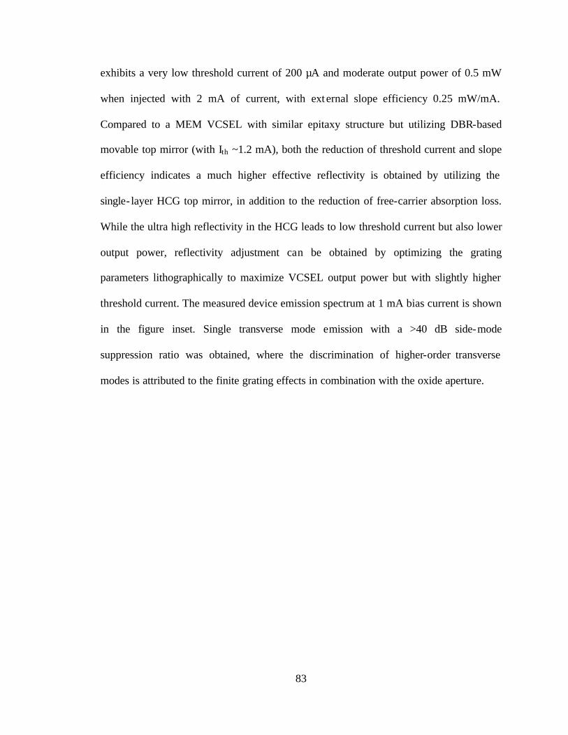
83
exhibits a very low threshold current of 200 µA and moderate output power of 0.5 mW
when injected with 2 mA of current, with ext ernal slope efficiency 0.25 mW/mA.
Compared to a MEM VCSEL with similar epitaxy structure but utilizing DBR-based
movable top mirror (with Ith ~1.2 mA), both the reduction of threshold current and slope
efficiency indicates a much higher effective reflectivity is obtained by utilizing the
single- layer HCG top mirror, in addition to the reduction of free-carrier absorption loss.
While the ultra high reflectivity in the HCG leads to low threshold current but also lower
output power, reflectivity adjustment can be obtained by optimizing the grating
parameters lithographically to maximize VCSEL output power but with slightly higher
threshold current. The measured device emission spectrum at 1 mA bias current is shown
in the figure inset. Single transverse mode emission with a >40 dB side-mode
suppression ratio was obtained, where the discrimination of higher-order transverse
modes is attributed to the finite grating effects in combination with the oxide aperture.
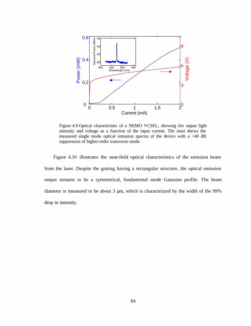
84
0 0.5 1 1.5 20
0.2
0.4
0.6
Current (mA)
Pow
er (
mW
)
0
3
6
9
Vol
tage
(V
)
840 845 850 855
-80
-60
-40
-20
Wavelength (nm)
Spe
ctra
l Pow
er (d
Bm
)
845 850Wavelength (nm)
0 0.5 1 1.5 20
0.2
0.4
0.6
Current (mA)
Pow
er (
mW
)
0
3
6
9
Vol
tage
(V
)
840 845 850 855
-80
-60
-40
-20
Wavelength (nm)
Spe
ctra
l Pow
er (d
Bm
)
845 850Wavelength (nm)
Figure 4.9 Optical characteristic of a NEMO VCSEL, showing the output light intensity and voltage as a function of the input current. The inset shows the measured single mode optical emission spectra of the device with a >40 dB suppression of higher-order transverse mode.
Figure 4.10 illustrates the near-field optical characteristics of the emission beam
from the laser. Despite the grating having a rectangular structure, the optical emission
output remains to be a symmetrical, fundamental mode Gaussian profile. The beam
diameter is measured to be about 3 µm, which is characterized by the width of the 99%
drop in intensity.
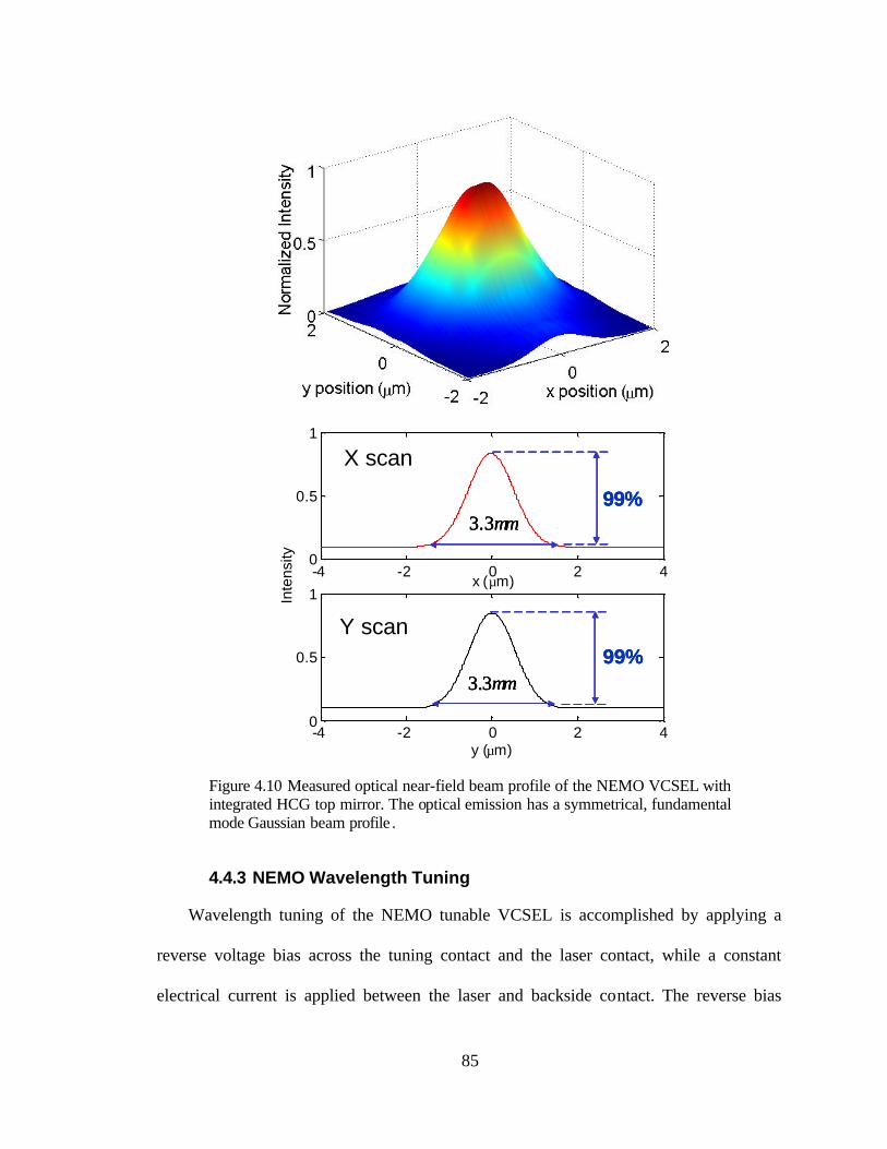
85
-4 -2 0 2 40
0.5
1
x (µm)
-4 -2 0 2 40
0.5
1
y (µm)
Inte
nsity
X scan
Y scan
mµ3.399%
mµ3.399%
-4 -2 0 2 40
0.5
1
x (µm)
-4 -2 0 2 40
0.5
1
y (µm)
Inte
nsity
X scan
Y scan
-4 -2 0 2 40
0.5
1
x (µm)
-4 -2 0 2 40
0.5
1
y (µm)
Inte
nsity
X scan
Y scan
mµ3.399%
mµ3.399%
mµ3.399%
mµ3.399%
mµ3.399%
mµ3.399%
Figure 4.10 Measured optical near-field beam profile of the NEMO VCSEL with integrated HCG top mirror. The optical emission has a symmetrical, fundamental mode Gaussian beam profile .
4.4.3 NEMO Wavelength Tuning
Wavelength tuning of the NEMO tunable VCSEL is accomplished by applying a
reverse voltage bias across the tuning contact and the laser contact, while a constant
electrical current is applied between the laser and backside contact. The reverse bias
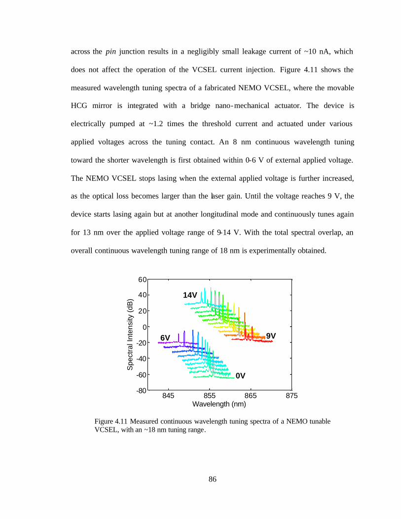
86
across the pin junction results in a negligibly small leakage current of ~10 nA, which
does not affect the operation of the VCSEL current injection. Figure 4.11 shows the
measured wavelength tuning spectra of a fabricated NEMO VCSEL, where the movable
HCG mirror is integrated with a bridge nano-mechanical actuator. The device is
electrically pumped at ~1.2 times the threshold current and actuated under various
applied voltages across the tuning contact. An 8 nm continuous wavelength tuning
toward the shorter wavelength is first obtained within 0-6 V of external applied voltage.
The NEMO VCSEL stops lasing when the external applied voltage is further increased,
as the optical loss becomes larger than the laser gain. Until the voltage reaches 9 V, the
device starts lasing again but at another longitudinal mode and continuously tunes again
for 13 nm over the applied voltage range of 9-14 V. With the total spectral overlap, an
overall continuous wavelength tuning range of 18 nm is experimentally obtained.
845 855 865 875-80
-60
-40
-20
0
20
40
60
Wavelength (nm)
Spe
ctra
l Int
ensi
ty (d
B)
0V
6V 9V
14V
845 855 865 875-80
-60
-40
-20
0
20
40
60
Wavelength (nm)
Spe
ctra
l Int
ensi
ty (d
B)
0V
6V 9V
14V
Figure 4.11 Measured continuous wavelength tuning spectra of a NEMO tunable VCSEL, with an ~18 nm tuning range.
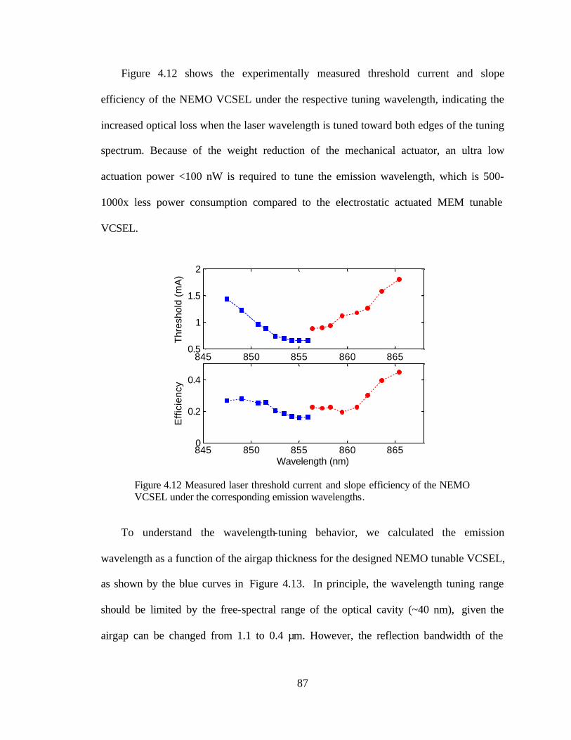
87
Figure 4.12 shows the experimentally measured threshold current and slope
efficiency of the NEMO VCSEL under the respective tuning wavelength, indicating the
increased optical loss when the laser wavelength is tuned toward both edges of the tuning
spectrum. Because of the weight reduction of the mechanical actuator, an ultra low
actuation power <100 nW is required to tune the emission wavelength, which is 500-
1000x less power consumption compared to the electrostatic actuated MEM tunable
VCSEL.
845 850 855 860 8650.5
1
1.5
2
Thr
esho
ld (
mA
)
845 850 855 860 8650
0.2
0.4
Wavelength (nm)
Effi
cien
cy
Figure 4.12 Measured laser threshold current and slope efficiency of the NEMO VCSEL under the corresponding emission wavelengths.
To understand the wavelength-tuning behavior, we calculated the emission
wavelength as a function of the airgap thickness for the designed NEMO tunable VCSEL,
as shown by the blue curves in Figure 4.13. In principle, the wavelength tuning range
should be limited by the free-spectral range of the optical cavity (~40 nm), given the
airgap can be changed from 1.1 to 0.4 µm. However, the reflection bandwidth of the

88
HCG top mirror also varies as the airgap changes, since the airgap also contributes to the
overall mirror reflectivity depending on its optical length [51]. Hence our measured
wavelength tuning range of 18 nm is limited by the drop in the mirror reflectivity as the
cavity wavelength detunes from the center, which results in a higher threshold gain
required for achieving the lasing condition. This is in agreement with the observed
increase of threshold current at both edges of the tuning spectrum shown in Figure 4.12.
The wavelength limitation originates from the smaller reflection bandwidth of the HCG
mirror (shown by the white curve), since the current design is intentionally engineered to
yield a large fabrication tolerance. We anticipate a larger wavelength tuning range of 35-
40 nm can be attained by using an HCG top mirror designed to yield a much broader
reflection bandwidth, so the wavelength tuning curve overlaps entirely within the high
reflectivity bandwidth of HCG as shown in Figure 4.13.
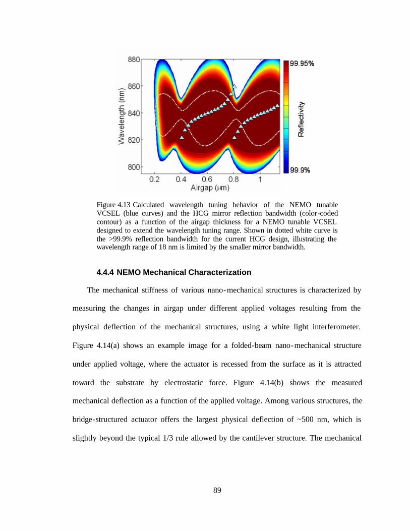
89
Figure 4.13 Calculated wavelength tuning behavior of the NEMO tunable VCSEL (blue curves) and the HCG mirror reflection bandwidth (color-coded contour) as a function of the airgap thickness for a NEMO tunable VCSEL designed to extend the wavelength tuning range. Shown in dotted white curve is the >99.9% reflection bandwidth for the current HCG design, illustrating the wavelength range of 18 nm is limited by the smaller mirror bandwidth.
4.4.4 NEMO Mechanical Characterization
The mechanical stiffness of various nano-mechanical structures is characterized by
measuring the changes in airgap under different applied voltages resulting from the
physical deflection of the mechanical structures, using a white light interferometer.
Figure 4.14(a) shows an example image for a folded-beam nano-mechanical structure
under applied voltage, where the actuator is recessed from the surface as it is attracted
toward the substrate by electrostatic force. Figure 4.14(b) shows the measured
mechanical deflection as a function of the applied voltage. Among various structures, the
bridge-structured actuator offers the largest physical deflection of ~500 nm, which is
slightly beyond the typical 1/3 rule allowed by the cantilever structure. The mechanical
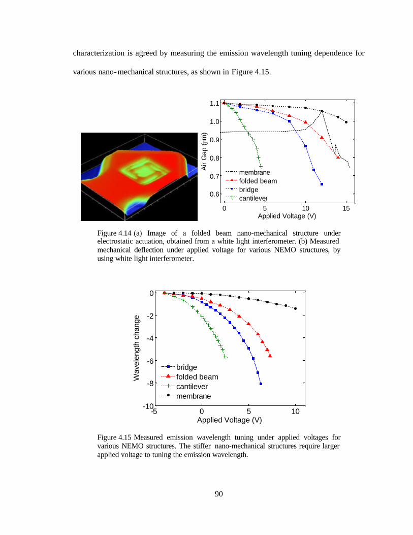
90
characterization is agreed by measuring the emission wavelength tuning dependence for
various nano-mechanical structures, as shown in Figure 4.15.
0 5 10 15
0.6
0.7
0.8
0.9
1.0
1.1
Applied Voltage (V)
Air
Gap
(µm
)
membranefolded beambridgecantilever
0 5 10 15
0.6
0.7
0.8
0.9
1.0
1.1
Applied Voltage (V)
Air
Gap
(µm
)
membranefolded beambridgecantilever
Figure 4.14 (a) Image of a folded beam nano-mechanical structure under electrostatic actuation, obtained from a white light interferometer. (b) Measured mechanical deflection under applied voltage for various NEMO structures, by using white light interferometer.
-5 0 5 10-10
-8
-6
-4
-2
0
Applied Voltage (V)
Wav
elen
gth
chan
ge
bridgefolded beamcantilevermembrane
Figure 4.15 Measured emission wavelength tuning under applied voltages for various NEMO structures. The stiffer nano-mechanical structures require larger applied voltage to tuning the emission wavelength.
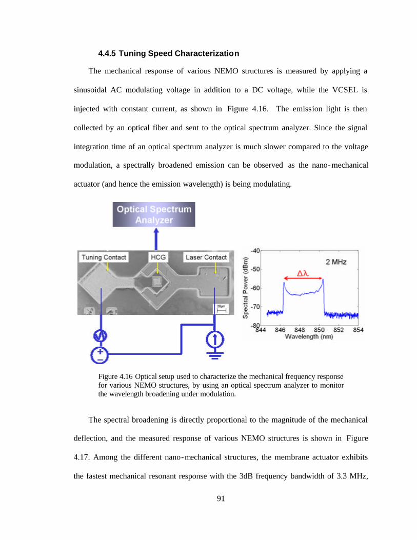
91
4.4.5 Tuning Speed Characterization
The mechanical response of various NEMO structures is measured by applying a
sinusoidal AC modulating voltage in addition to a DC voltage, while the VCSEL is
injected with constant current, as shown in Figure 4.16. The emission light is then
collected by an optical fiber and sent to the optical spectrum analyzer. Since the signal
integration time of an optical spectrum analyzer is much slower compared to the voltage
modulation, a spectrally broadened emission can be observed as the nano-mechanical
actuator (and hence the emission wavelength) is being modulating.
Figure 4.16 Optical setup used to characterize the mechanical frequency response for various NEMO structures, by using an optical spectrum analyzer to monitor the wavelength broadening under modulation.
The spectral broadening is directly proportional to the magnitude of the mechanical
deflection, and the measured response of various NEMO structures is shown in Figure
4.17. Among the different nano-mechanical structures, the membrane actuator exhibits
the fastest mechanical resonant response with the 3dB frequency bandwidth of 3.3 MHz,
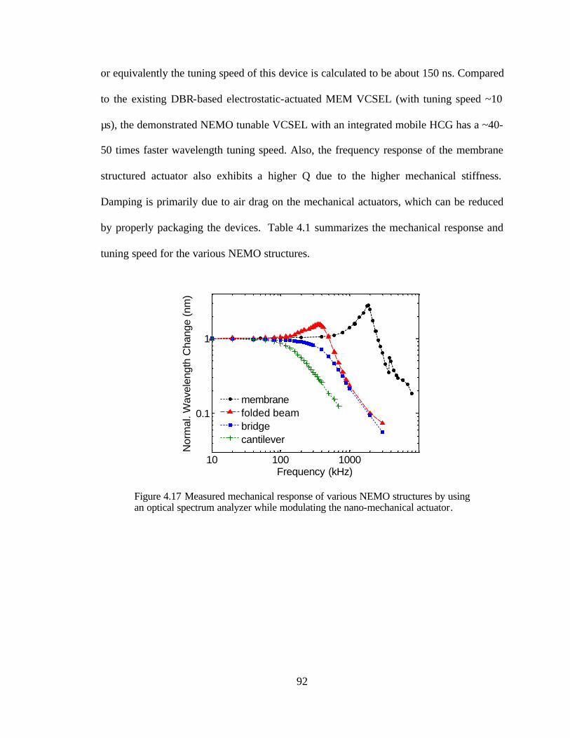
92
or equivalently the tuning speed of this device is calculated to be about 150 ns. Compared
to the existing DBR-based electrostatic-actuated MEM VCSEL (with tuning speed ~10
µs), the demonstrated NEMO tunable VCSEL with an integrated mobile HCG has a ~40-
50 times faster wavelength tuning speed. Also, the frequency response of the membrane
structured actuator also exhibits a higher Q due to the higher mechanical stiffness.
Damping is primarily due to air drag on the mechanical actuators, which can be reduced
by properly packaging the devices. Table 4.1 summarizes the mechanical response and
tuning speed for the various NEMO structures.
10 100 1000
0.1
1
Frequency (kHz)
Nor
mal
. Wav
elen
gth
Cha
nge
(nm
)
membranefolded beambridgecantilever
Figure 4.17 Measured mechanical response of various NEMO structures by using an optical spectrum analyzer while modulating the nano-mechanical actuator.
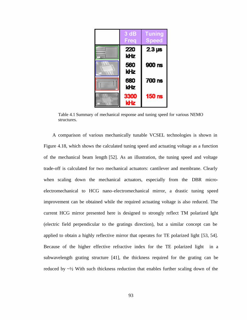
93
Table 4.1 Summary of mechanical response and tuning speed for various NEMO structures.
A comparison of various mechanically tunable VCSEL technologies is shown in
Figure 4.18, which shows the calculated tuning speed and actuating voltage as a function
of the mechanical beam length [52]. As an illustration, the tuning speed and voltage
trade-off is calculated for two mechanical actuators: cantilever and membrane. Clearly
when scaling down the mechanical actuators, especially from the DBR micro-
electromechanical to HCG nano-electromechanical mirror, a drastic tuning speed
improvement can be obtained while the required actuating voltage is also reduced. The
current HCG mirror presented here is designed to strongly reflect TM polarized light
(electric field perpendicular to the gratings direction), but a similar concept can be
applied to obtain a highly reflective mirror that operates for TE polarized light [53, 54].
Because of the higher effective refractive index for the TE polarized light in a
subwavelength grating structure [41], the thickness required for the grating can be
reduced by ~½. With such thickness reduction that enables further scaling down of the
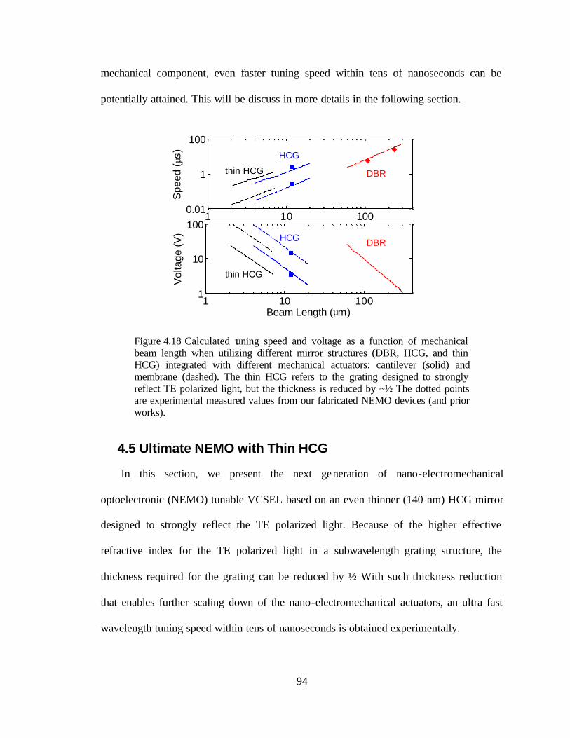
94
mechanical component, even faster tuning speed within tens of nanoseconds can be
potentially attained. This will be discuss in more details in the following section.
1 10 1000.01
1
100
Spe
ed (µ
s)
1 10 1001
10
100
Beam Length (µm)
Vol
tage
(V)
DBR
HCG
thin HCG
DBRHCG
thin HCG
1 10 1000.01
1
100
Spe
ed (µ
s)
1 10 1001
10
100
Beam Length (µm)
Vol
tage
(V)
DBR
HCG
thin HCG
DBRHCG
thin HCG
Figure 4.18 Calculated tuning speed and voltage as a function of mechanical beam length when utilizing different mirror structures (DBR, HCG, and thin HCG) integrated with different mechanical actuators: cantilever (solid) and membrane (dashed). The thin HCG refers to the grating designed to strongly reflect TE polarized light, but the thickness is reduced by ~½. The dotted points are experimental measured values from our fabricated NEMO devices (and prior works).
4.5 Ultimate NEMO with Thin HCG
In this section, we present the next generation of nano-electromechanical
optoelectronic (NEMO) tunable VCSEL based on an even thinner (140 nm) HCG mirror
designed to strongly reflect the TE polarized light. Because of the higher effective
refractive index for the TE polarized light in a subwavelength grating structure, the
thickness required for the grating can be reduced by ½. With such thickness reduction
that enables further scaling down of the nano-electromechanical actuators, an ultra fast
wavelength tuning speed within tens of nanoseconds is obtained experimentally.
95
4.5.1 TE HCG Design
The schematic of the device is shown in Figure 4.19(a), which consists of a bottom
34-pairs n-DBR, a cavity layer with the quantum well active region, and a freely
suspended n-doped single- layer HCG top mirror that is supported via a nano-
electromechanical structure. Electric current injection is conducted through the middle
laser contact (via 4 pairs of p-DBR above cavity) and backside contact. An aluminum
oxide aperture is formed on an AlAs layer in the p-DBR section above the cavity layer to
provide current and optical confinement. The tuning contact is fabricated on the top n-
doped HCG layer. Figure 4.19(b) shows the top view SEM image of the fabricated
device with the HCG aligned in the center of the VCSEL mesa (oxide aperture). Fig.
Figure 4.19(c) and (d) shows the comparison of the grating thickness in a TM-design
HCG and a TE-design HCG, respectively. Clearly the TE-design HCG contains grating
stripes with half the thickness of that of TM-design HCG, and hence the mechanical
weight is reduced by ½ . Meanwhile, both HCGs provide similar ultra high reflectivity
and bandwidth required for VCSELs as the top mirror, as shown in Figure 4.20.
96
Figure 4.19 The ultimate NEMO tunable VCSEL utilizing a freely suspended HCG top mirror. (a) The device schematic showing the epitaxial design. (b) SEM image of the fabricated device, where the HCG is integrated with a nano-electromechanical actuator. (c) SEM image showing the grating thickness (235 nm) of a TM-HCG. (d) SEM showing the grating thickness (140 nm) of a TE- HCG.
97
0.7 0.8 0.9 1 1.10
0.2
0.4
0.6
0.8
1
Wavelength (µm)
Ref
lect
ivity
TM-HCGTE-HCG
0.8 0.85 0.90.999
0.9994
0.9998
Wavelength (µm)
Ref
lect
ivity
0.7 0.8 0.9 1 1.10
0.2
0.4
0.6
0.8
1
Wavelength (µm)
Ref
lect
ivity
TM-HCGTE-HCG
0.8 0.85 0.90.999
0.9994
0.9998
Wavelength (µm)
Ref
lect
ivity
Figure 4.20 Calculated reflectivity of a TM-design and a TE-design HCG, each with TM and TE polarized incident surface-normal plane wave, respectively.
4.5.2 Optical Characteristics
Continuous wave operation of an electrostatic actuated NEMO tunable VCSEL with
excellent optical performance was demonstrated. Figure 4.21 shows the VCSEL optical
measurement, showing the output power versus bias current (LI) and voltage versus bias
current (IV) characteristics. The VCSEL device exhibits a low threshold current of 1.0
mA and high output power of ~2 mW when injected with 5 mA of current, with slope
efficiency 0.54 W/A.
98
0 1 2 3 4 50
0.5
1
1.5
2
Current (mA)
Pow
er (m
W)
0 1 2 3 4 50
2
4
6
8
Vol
tage
(V)
Ith=1.08 P=2 η=0.54 R=5.4e+002
0 1 2 3 4 50
0.5
1
1.5
2
Current (mA)
Pow
er (m
W)
0 1 2 3 4 50
2
4
6
8
Vol
tage
(V)
Ith=1.08 P=2 η=0.54 R=5.4e+002
Figure 4.21 Measured light intensity versus current characteristic of a NEMO utilizing a TE-HCG (140 nm). A high output power of 2 mW is obtained at 5 mA of injected current.
Figure 4.22 shows the measured emission spectra of the laser when biased at 4 times
the Ith. Since the high reflectivity is only available within the finite HCG pattern area,
higher-order transverse modes are suppressed and a single fundamental mode emission
with a 45 dB side-mode suppression ratio (SMSR) was obtained.
850 852 854 856 858 860
-80
-70
-60
-50
-40
-30
-20
Wavelength (nm)
Spe
ctra
l Pow
er (d
Bm
)
45 dB
850 852 854 856 858 860
-80
-70
-60
-50
-40
-30
-20
Wavelength (nm)
Spe
ctra
l Pow
er (d
Bm
)
45 dB
Figure 4.22 Measured emission spectra of a fabricated 3 µm aperture HCG VCSEL using a TE HCG top mirror, when biased at 4 time the Ith..
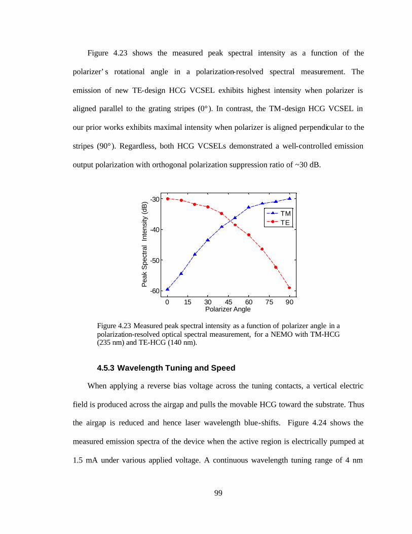
99
Figure 4.23 shows the measured peak spectral intensity as a function of the
polarizer’s rotational angle in a polarization-resolved spectral measurement. The
emission of new TE-design HCG VCSEL exhibits highest intensity when polarizer is
aligned parallel to the grating stripes (0°). In contrast, the TM-design HCG VCSEL in
our prior works exhibits maximal intensity when polarizer is aligned perpendicular to the
stripes (90°). Regardless, both HCG VCSELs demonstrated a well-controlled emission
output polarization with orthogonal polarization suppression ratio of ~30 dB.
0 15 30 45 60 75 90
-60
-50
-40
-30
Polarizer Angle
Pea
k S
pect
ral
Inte
nsity
(dB
)
TMTE
Figure 4.23 Measured peak spectral intensity as a function of polarizer angle in a polarization-resolved optical spectral measurement, for a NEMO with TM-HCG (235 nm) and TE-HCG (140 nm).
4.5.3 Wavelength Tuning and Speed
When applying a reverse bias voltage across the tuning contacts, a vertical electric
field is produced across the airgap and pulls the movable HCG toward the substrate. Thus
the airgap is reduced and hence laser wavelength blue-shifts. Figure 4.24 shows the
measured emission spectra of the device when the active region is electrically pumped at
1.5 mA under various applied voltage. A continuous wavelength tuning range of 4 nm
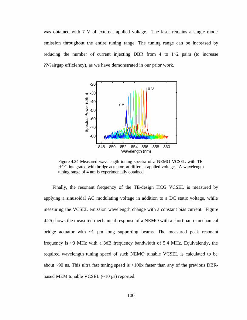
100
was obtained with 7 V of external applied voltage. The laser remains a single mode
emission throughout the entire tuning range. The tuning range can be increased by
reducing the number of current injecting DBR from 4 to 1~2 pairs (to increase
??/?airgap efficiency), as we have demonstrated in our prior work.
848 850 852 854 856 858 860
-80
-70
-60
-50
-40
-30
-20
Wavelength (nm)
Spe
ctra
l Pow
er (d
Bm
)0 V
7 V
848 850 852 854 856 858 860
-80
-70
-60
-50
-40
-30
-20
Wavelength (nm)
Spe
ctra
l Pow
er (d
Bm
)0 V
7 V
Figure 4.24 Measured wavelength tuning spectra of a NEMO VCSEL with TE-HCG integrated with bridge actuator, at different applied voltages. A wavelength tuning range of 4 nm is experimentally obtained.
Finally, the resonant frequency of the TE-design HCG VCSEL is measured by
applying a sinusoidal AC modulating voltage in addition to a DC static voltage, while
measuring the VCSEL emission wavelength change with a constant bias current. Figure
4.25 shows the measured mechanical response of a NEMO with a short nano-mechanical
bridge actuator with ~1 µm long supporting beams. The measured peak resonant
frequency is ~3 MHz with a 3dB frequency bandwidth of 5.4 MHz. Equivalently, the
required wavelength tuning speed of such NEMO tunable VCSEL is calculated to be
about ~90 ns. This ultra fast tuning speed is >100x faster than any of the previous DBR-
based MEM tunable VCSEL (~10 µs) reported.
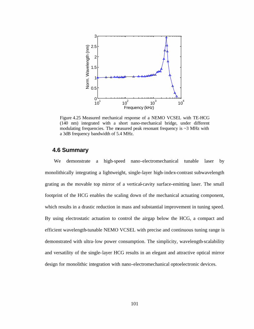
101
101
102
103
1040
0.5
1
1.5
2
2.5
3
Frequency (kHz)
Nor
m. W
avel
engt
h (n
m)
Figure 4.25 Measured mechanical response of a NEMO VCSEL with TE-HCG (140 nm) integrated with a short nano-mechanical bridge, under different modulating frequencies. The measured peak resonant frequency is ~3 MHz with a 3dB frequency bandwidth of 5.4 MHz.
4.6 Summary
We demonstrate a high-speed nano-electromechanical tunable laser by
monolithically integrating a lightweight, single-layer high- index-contrast subwavelength
grating as the movable top mirror of a vertical-cavity surface-emitting laser. The small
footprint of the HCG enables the scaling down of the mechanical actuating component,
which results in a drastic reduction in mass and substantial improvement in tuning speed.
By using electrostatic actuation to control the airgap below the HCG, a compact and
efficient wavelength-tunable NEMO VCSEL with precise and continuous tuning range is
demonstrated with ultra- low power consumption. The simplicity, wavelength-scalability
and versatility of the single- layer HCG results in an elegant and attractive optical mirror
design for monolithic integration with nano-electromechanical optoelectronic devices.
102
Chapter 5 Piezoelectric Actuated MEM Tunable VCSEL
5.1 Motivation
The integration of micro-electromechanical (MEM) or nano-electromechanical
(NEM) tunable structures with vertical-cavity surface-emitting lasers (VCSEL) can result
in a wavelength-tunable light source. Beside the compatibility with the current
optoelectronic fabrication process, the mechanically tunable lasers can provide a large
and continuous wavelength tuning range with high precision. The MEM tunable VCSEL
has the majority part of its top mirror being held by a micromechanical structure and it is
physically moved via electrostatic actuation. The physical movement changes the optical
cavity length and thus produces a change in the lasing wavelength. However, electrostatic
actuation is often limited by the 1/3 rule, where the maximum mechanical deflection can
be at most 1/3 of the original airgap spacing. This maximum deflection characteristic can
be seen from equation (5.1), which is derived from the equilibrium condition where the
electrostatic force is set equals to the hooks restoring force of the mechanical beam. The
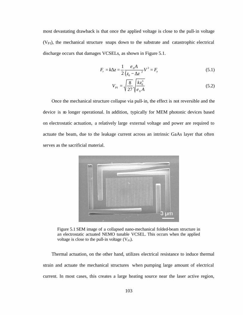
103
most devastating drawback is that once the applied voltage is close to the pull- in voltage
(VPI), the mechanical structure snaps down to the substrate and catastrophic electrical
discharge occurs that damages VCSELs, as shown in Figure 5.1.
( ) er FVzz
AzkF =
∆−=∆= 2
20
0
21 ε
(5.1)
A
kzVPI
0
30
278
ε= (5.2)
Once the mechanical structure collapse via pull- in, the effect is not reversible and the
device is no longer operational. In addition, typically for MEM photonic devices based
on electrostatic actuation, a relatively large external voltage and power are required to
actuate the beam, due to the leakage current across an intrinsic GaAs layer that often
serves as the sacrificial material.
Figure 5.1 SEM image of a collapsed nano-mechanical folded-beam structure in an electrostatic actuated NEMO tunable VCSEL. This occurs when the applied voltage is close to the pull-in voltage (VPI).
Thermal actuation, on the other hand, utilizes electrical resistance to induce thermal
strain and actuate the mechanical structures when pumping large amount of electrical
current. In most cases, this creates a large heating source near the laser active region,
104
which may adversely affect the laser’s reliability and performance. In addition, the
actuation speed is fairly low (~100 Hz) due to long thermal transient time and thermal
actuation generally requires high actuation power.
In this chapter, we proposed a monolithic integrated piezoelectric actuated
wavelength-tunable VCSEL that exploits the inherent piezoelectric properties of AlxGa1-
xAs compounds. Piezoelectric actuation offers several potential advantages. First, it can
provide large mechanical deflections in bi-directions, both towards the substrate and
opposite to it. The movement is not limited by pull- in effect, as opposed to the 1/3 gap
limit associated with electrostatic actuation. More importantly, there will be no
catastrophic damage due to capacitor discharge, which is quite important in terms of
device reliability. It is expected to consume low power (~1 µW), and has a relatively fast
response speed (limited only by the mechanical structure rather than the piezoelectric
effect). Mechanical movement using piezoelectric effect has the advantages of high
electro-mechanical coupling strength and linear response, compared to electrostatic
actuation. Finally, piezoelectric actuation can be readily extended to other MEM tunable
optoelectronic devices operating at different wavelengths. As a demonstration, we
implemented the monolithic piezoelectric actuation onto the convention DBR-based
MEM tunable VCSEL.
5.2 Piezoelectric Actuation in AlGaAs
The piezoelectric property of AlGaAs is an inherent characteristic that originates
from the zinc-blend crystalline structure that lacks center inversion symmetry. Under the
presence of a vertical electric field, an intrinsic AlGaAs beam is subject to a longitudinal
strain caused by internal polarization that results in a change in its length (?L). The
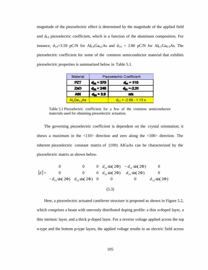
105
magnitude of the piezoelectric effect is determined by the magnitude of the applied field
and d14 piezoelectric coefficient, which is a function of the aluminum composition. For
instance, d14=3.59 pC/N for Al0.8Ga0.2As and d14 = 2.80 pC/N for Al0.1Ga0.9As. The
piezoelectric coefficient for some of the common semiconductor material that exhibits
piezoelectric properties is summarized below in Table 5.1.
Table 5.1 Piezoelectric coefficient for a few of the common semiconductor materials used for obtaining piezoelectric actuation.
The governing piezoelectric coefficient is dependent on the crystal orientation; it
shows a maximum in the <110> direction and zero along the <100> direction. The
inherent piezoelectric constant matrix of (100) AlGaAs can be characterized by the
piezoelectric matrix as shown below.
[ ]
ΦΦΦ−ΦΦ
Φ−Φ
=)2sin(000)2sin()2sin(
0)2sin()2sin(000
0)2sin()2sin(000
141414
1414
1414
ddddd
dd
d
(5.3)
Here, a piezoelectric actuated cantilever structure is proposed as shown in Figure 5.2,
which comprises a beam with unevenly distributed doping profile: a thin n-doped layer, a
thin intrinsic layer, and a thick p-doped layer. For a reverse voltage applied across the top
n-type and the bottom p-type layers, the applied voltage results in an electric field across
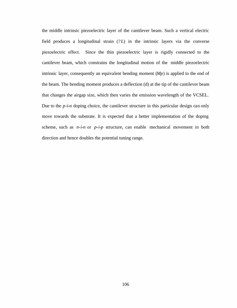
106
the middle intrinsic piezoelectric layer of the cantilever beam. Such a vertical electric
field produces a longitudinal strain (? L) in the intrinsic layers via the converse
piezoelectric effect. Since the thin piezoelectric layer is rigidly connected to the
cantilever beam, which constrains the longitudinal motion of the middle piezoelectric
intrinsic layer, consequently an equivalent bending moment (Mp) is applied to the end of
the beam. The bending moment produces a deflection (d) at the tip of the cantilever beam
that changes the airgap size, which then varies the emission wavelength of the VCSEL.
Due to the p-i-n doping choice, the cantilever structure in this particular design can only
move towards the substrate. It is expected that a better implementation of the doping
scheme, such as n-i-n or p-i-p structure, can enable mechanical movement in both
direction and hence doubles the potential tuning range.
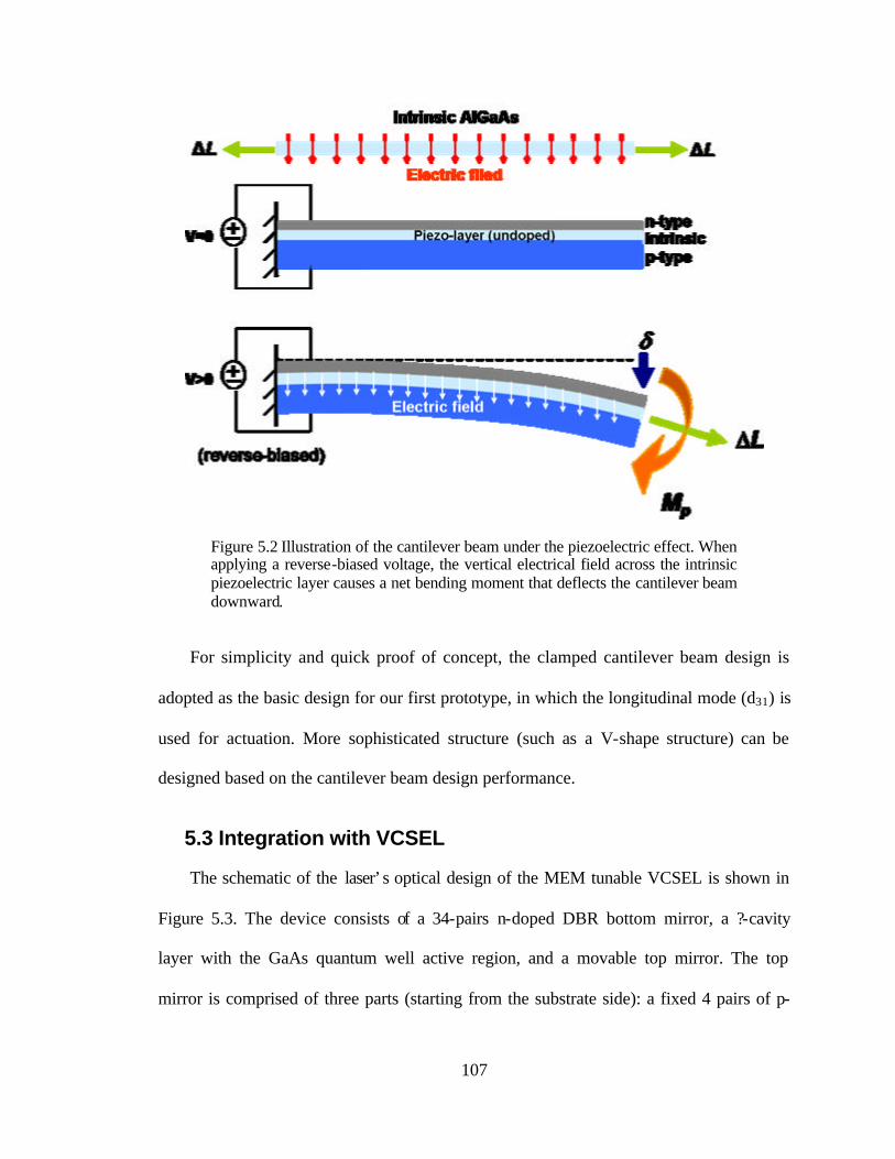
107
Figure 5.2 Illustration of the cantilever beam under the piezoelectric effect. When applying a reverse-biased voltage, the vertical electrical field across the intrinsic piezoelectric layer causes a net bending moment that deflects the cantilever beam downward.
For simplicity and quick proof of concept, the clamped cantilever beam design is
adopted as the basic design for our first prototype, in which the longitudinal mode (d31) is
used for actuation. More sophisticated structure (such as a V-shape structure) can be
designed based on the cantilever beam design performance.
5.3 Integration with VCSEL
The schematic of the laser’s optical design of the MEM tunable VCSEL is shown in
Figure 5.3. The device consists of a 34-pairs n-doped DBR bottom mirror, a ?-cavity
layer with the GaAs quantum well active region, and a movable top mirror. The top
mirror is comprised of three parts (starting from the substrate side): a fixed 4 pairs of p-
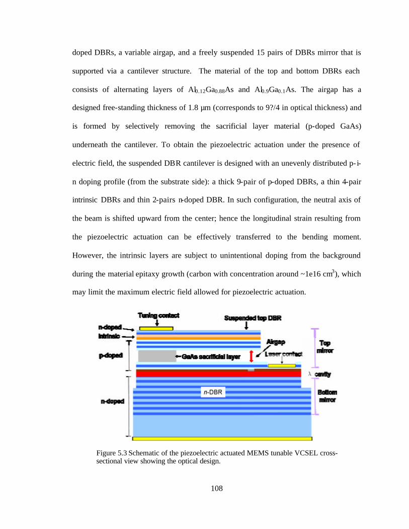
108
doped DBRs, a variable airgap, and a freely suspended 15 pairs of DBRs mirror that is
supported via a cantilever structure. The material of the top and bottom DBRs each
consists of alternating layers of Al0.12Ga0.88As and Al0.9Ga0.1As. The airgap has a
designed free-standing thickness of 1.8 µm (corresponds to 9?/4 in optical thickness) and
is formed by selectively removing the sacrificial layer material (p-doped GaAs)
underneath the cantilever. To obtain the piezoelectric actuation under the presence of
electric field, the suspended DBR cantilever is designed with an unevenly distributed p- i-
n doping profile (from the substrate side): a thick 9-pair of p-doped DBRs, a thin 4-pair
intrinsic DBRs and thin 2-pairs n-doped DBR. In such configuration, the neutral axis of
the beam is shifted upward from the center; hence the longitudinal strain resulting from
the piezoelectric actuation can be effectively transferred to the bending moment.
However, the intrinsic layers are subject to unintentional doping from the background
during the material epitaxy growth (carbon with concentration around ~1e16 cm3), which
may limit the maximum electric field allowed for piezoelectric actuation.
Figure 5.3 Schematic of the piezoelectric actuated MEMS tunable VCSEL cross-sectional view showing the optical design.
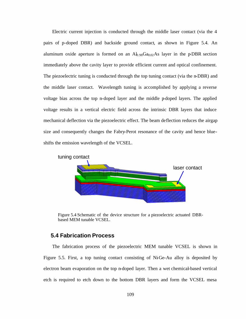
109
Electric current injection is conducted through the middle laser contact (via the 4
pairs of p-doped DBR) and backside ground contact, as shown in Figure 5.4. An
aluminum oxide aperture is formed on an Al0.98Ga0.02As layer in the p-DBR section
immediately above the cavity layer to provide efficient current and optical confinement.
The piezoelectric tuning is conducted through the top tuning contact (via the n-DBR) and
the middle laser contact. Wavelength tuning is accomplished by applying a reverse
voltage bias across the top n-doped layer and the middle p-doped layers. The applied
voltage results in a vertical electric field across the intrinsic DBR layers that induce
mechanical deflection via the piezoelectric effect. The beam deflection reduces the airgap
size and consequently changes the Fabry-Perot resonance of the cavity and hence blue-
shifts the emission wavelength of the VCSEL.
tuning contact
laser contact
Figure 5.4 Schematic of the device structure for a piezoelectric actuated DBR-based MEM tunable VCSEL.
5.4 Fabrication Process
The fabrication process of the piezoelectric MEM tunable VCSEL is shown in
Figure 5.5. First, a top tuning contact consisting of Ni-Ge-Au alloy is deposited by
electron beam evaporation on the top n-doped layer. Then a wet chemical-based vertical
etch is required to etch down to the bottom DBR layers and form the VCSEL mesa
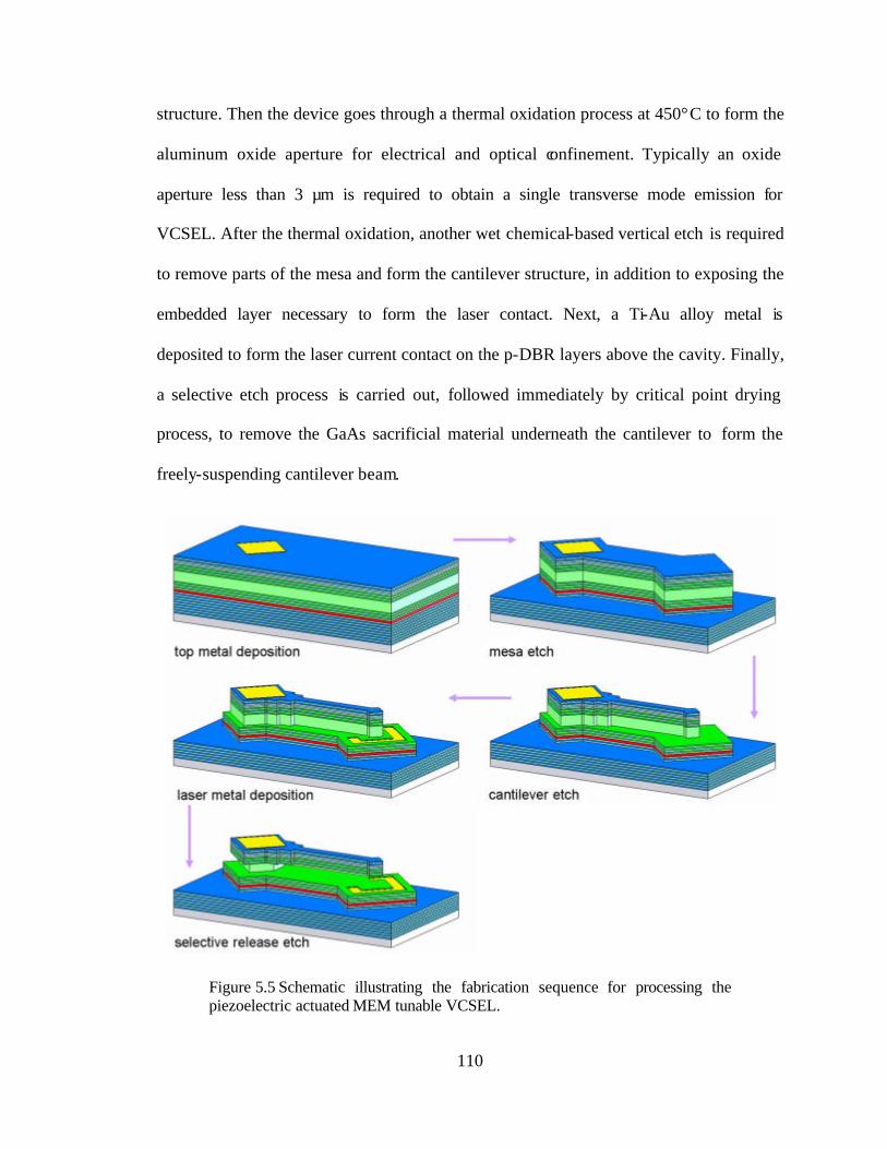
110
structure. Then the device goes through a thermal oxidation process at 450°C to form the
aluminum oxide aperture for electrical and optical confinement. Typically an oxide
aperture less than 3 µm is required to obtain a single transverse mode emission for
VCSEL. After the thermal oxidation, another wet chemical-based vertical etch is required
to remove parts of the mesa and form the cantilever structure, in addition to exposing the
embedded layer necessary to form the laser contact. Next, a Ti-Au alloy metal is
deposited to form the laser current contact on the p-DBR layers above the cavity. Finally,
a selective etch process is carried out, followed immediately by critical point drying
process, to remove the GaAs sacrificial material underneath the cantilever to form the
freely-suspending cantilever beam.
Figure 5.5 Schematic illustrating the fabrication sequence for processing the piezoelectric actuated MEM tunable VCSEL.
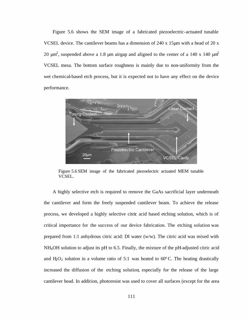
111
Figure 5.6 shows the SEM image of a fabricated piezoelectric-actuated tunable
VCSEL device. The cantilever beams has a dimension of 240 x 15µm with a head of 20 x
20 µm2, suspended above a 1.8 µm airgap and aligned to the center of a 140 x 140 µm2
VCSEL mesa. The bottom surface roughness is mainly due to non-uniformity from the
wet chemical-based etch process, but it is expected not to have any effect on the device
performance.
Figure 5.6 SEM image of the fabricated piezoelectric actuated MEM tunable VCSEL.
A highly selective etch is required to remove the GaAs sacrificial layer underneath
the cantilever and form the freely suspended cantilever beam. To achieve the release
process, we developed a highly selective citric acid based etching solution, which is of
critical importance for the success of our device fabrication. The etching solution was
prepared from 1:1 anhydrous citric acid: DI water (w/w). The citric acid was mixed with
NH4OH solution to adjust its pH to 6.5. Finally, the mixture of the pH-adjusted citric acid
and H2O2 solution in a volume ratio of 5:1 was heated to 60ºC. The heating drastically
increased the diffusion of the etching solution, especially for the release of the large
cantilever head. In addition, photoresist was used to cover all surfaces (except for the area
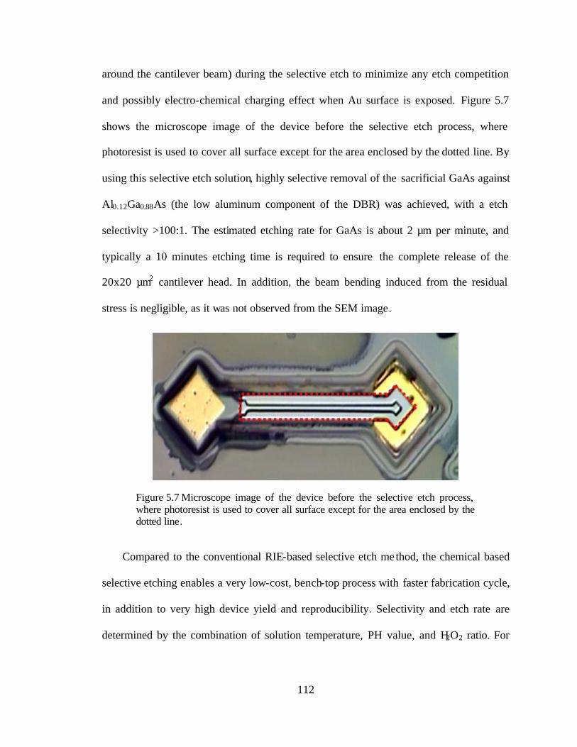
112
around the cantilever beam) during the selective etch to minimize any etch competition
and possibly electro-chemical charging effect when Au surface is exposed. Figure 5.7
shows the microscope image of the device before the selective etch process, where
photoresist is used to cover all surface except for the area enclosed by the dotted line. By
using this selective etch solution, highly selective removal of the sacrificial GaAs against
Al0.12Ga0.88As (the low aluminum component of the DBR) was achieved, with a etch
selectivity >100:1. The estimated etching rate for GaAs is about 2 µm per minute, and
typically a 10 minutes etching time is required to ensure the complete release of the
20x20 µm2 cantilever head. In addition, the beam bending induced from the residual
stress is negligible, as it was not observed from the SEM image.
Figure 5.7 Microscope image of the device before the selective etch process, where photoresist is used to cover all surface except for the area enclosed by the dotted line.
Compared to the conventional RIE-based selective etch method, the chemical based
selective etching enables a very low-cost, bench-top process with faster fabrication cycle,
in addition to very high device yield and reproducibility. Selectivity and etch rate are
determined by the combination of solution temperature, PH value, and H2O2 ratio. For
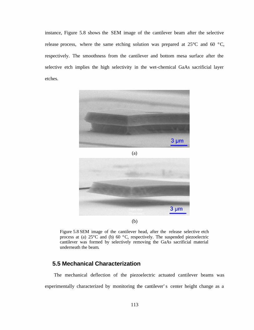
113
instance, Figure 5.8 shows the SEM image of the cantilever beam after the selective
release process, where the same etching solution was prepared at 25°C and 60 °C,
respectively. The smoothness from the cantilever and bottom mesa surface after the
selective etch implies the high selectivity in the wet-chemical GaAs sacrificial layer
etches.
(a)
(b)
Figure 5.8 SEM image of the cantilever head, after the release selective etch process at (a) 25°C and (b) 60 °C, respectively. The suspended piezoelectric cantilever was formed by selectively removing the GaAs sacrificial material underneath the beam.
5.5 Mechanical Characterization
The mechanical deflection of the piezoelectric actuated cantilever beams was
experimentally characterized by monitoring the cantilever’s center height change as a
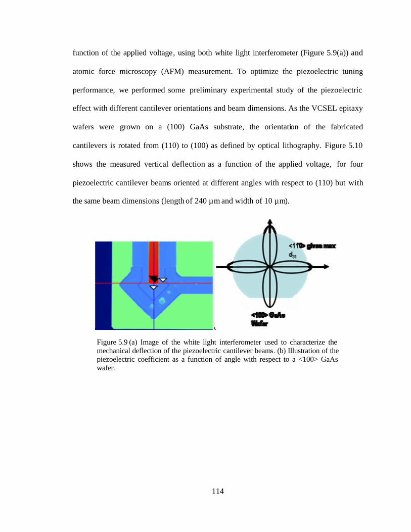
114
function of the applied voltage, using both white light interferometer (Figure 5.9(a)) and
atomic force microscopy (AFM) measurement. To optimize the piezoelectric tuning
performance, we performed some preliminary experimental study of the piezoelectric
effect with different cantilever orientations and beam dimensions. As the VCSEL epitaxy
wafers were grown on a (100) GaAs substrate, the orientation of the fabricated
cantilevers is rotated from (110) to (100) as defined by optical lithography. Figure 5.10
shows the measured vertical deflection as a function of the applied voltage, for four
piezoelectric cantilever beams oriented at different angles with respect to (110) but with
the same beam dimensions (length of 240 µm and width of 10 µm).
Figure 5.9 (a) Image of the white light interferometer used to characterize the mechanical deflection of the piezoelectric cantilever beams. (b) Illustration of the piezoelectric coefficient as a function of angle with respect to a <100> GaAs wafer.
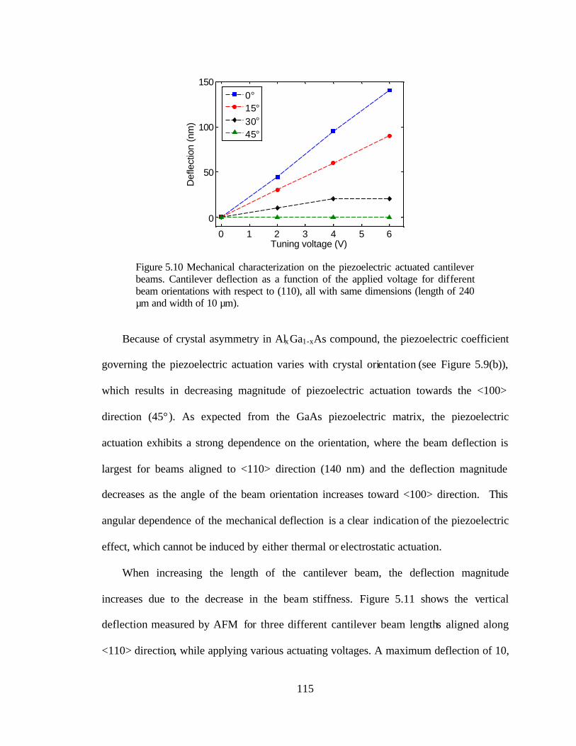
115
0 1 2 3 4 5 6
150
100
50
0
Tuning voltage (V)
Def
lect
ion
(nm
)
0°15°
30°
45°
Figure 5.10 Mechanical characterization on the piezoelectric actuated cantilever beams. Cantilever deflection as a function of the applied voltage for different beam orientations with respect to (110), all with same dimensions (length of 240 µm and width of 10 µm).
Because of crystal asymmetry in AlxGa1-xAs compound, the piezoelectric coefficient
governing the piezoelectric actuation varies with crystal orientation (see Figure 5.9(b)),
which results in decreasing magnitude of piezoelectric actuation towards the <100>
direction (45°). As expected from the GaAs piezoelectric matrix, the piezoelectric
actuation exhibits a strong dependence on the orientation, where the beam deflection is
largest for beams aligned to <110> direction (140 nm) and the deflection magnitude
decreases as the angle of the beam orientation increases toward <100> direction. This
angular dependence of the mechanical deflection is a clear indication of the piezoelectric
effect, which cannot be induced by either thermal or electrostatic actuation.
When increasing the length of the cantilever beam, the deflection magnitude
increases due to the decrease in the beam stiffness. Figure 5.11 shows the vertical
deflection measured by AFM for three different cantilever beam lengths aligned along
<110> direction, while applying various actuating voltages. A maximum deflection of 10,
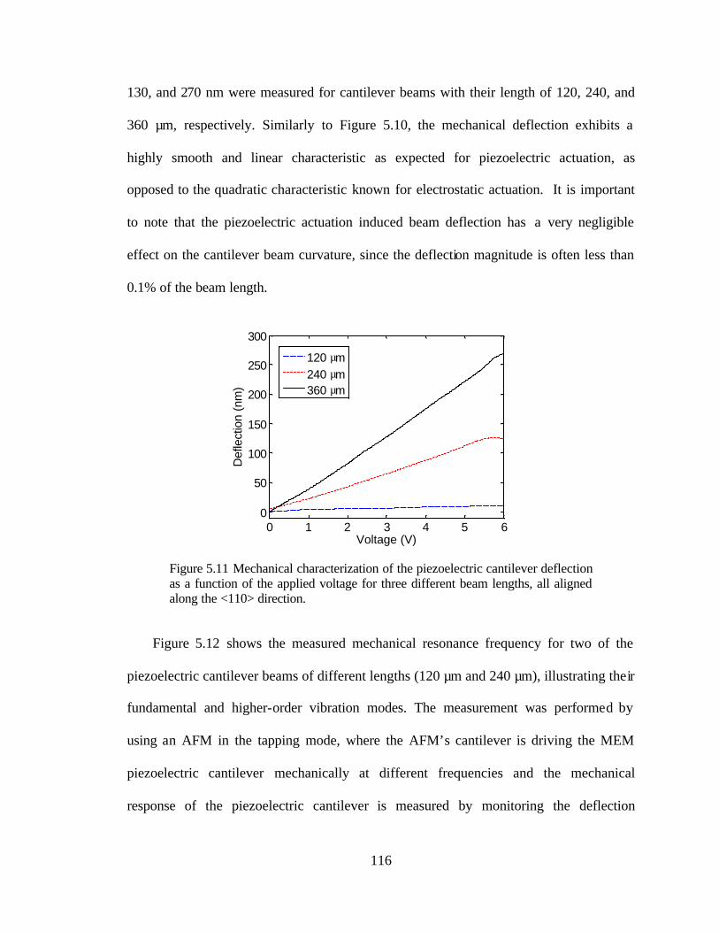
116
130, and 270 nm were measured for cantilever beams with their length of 120, 240, and
360 µm, respectively. Similarly to Figure 5.10, the mechanical deflection exhibits a
highly smooth and linear characteristic as expected for piezoelectric actuation, as
opposed to the quadratic characteristic known for electrostatic actuation. It is important
to note that the piezoelectric actuation induced beam deflection has a very negligible
effect on the cantilever beam curvature, since the deflection magnitude is often less than
0.1% of the beam length.
0 1 2 3 4 5 6
300
250
200
150
100
50
0
Voltage (V)
Def
lect
ion
(nm
)
120 µm240 µm360 µm
Figure 5.11 Mechanical characterization of the piezoelectric cantilever deflection as a function of the applied voltage for three different beam lengths, all aligned along the <110> direction.
Figure 5.12 shows the measured mechanical resonance frequency for two of the
piezoelectric cantilever beams of different lengths (120 µm and 240 µm), illustrating their
fundamental and higher-order vibration modes. The measurement was performed by
using an AFM in the tapping mode, where the AFM’s cantilever is driving the MEM
piezoelectric cantilever mechanically at different frequencies and the mechanical
response of the piezoelectric cantilever is measured by monitoring the deflection
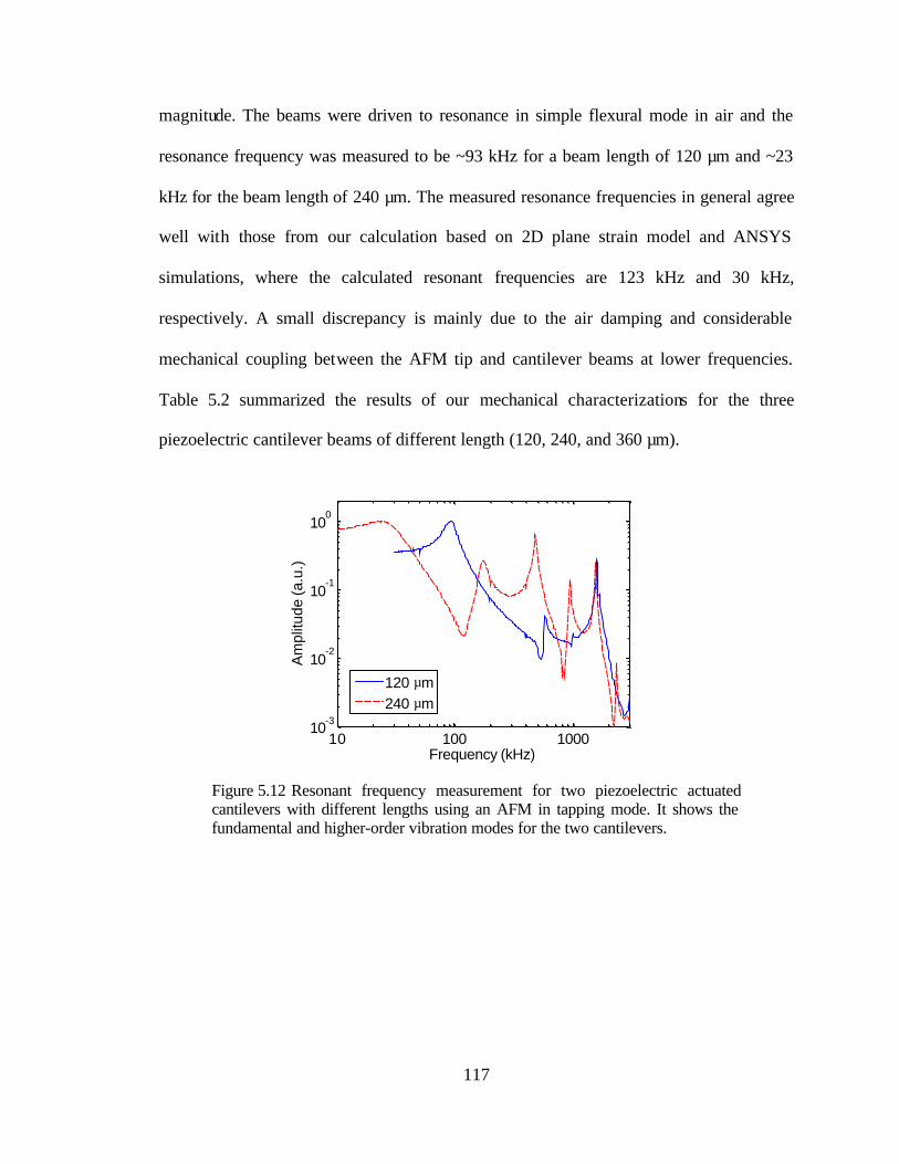
117
magnitude. The beams were driven to resonance in simple flexural mode in air and the
resonance frequency was measured to be ~93 kHz for a beam length of 120 µm and ~23
kHz for the beam length of 240 µm. The measured resonance frequencies in general agree
well with those from our calculation based on 2D plane strain model and ANSYS
simulations, where the calculated resonant frequencies are 123 kHz and 30 kHz,
respectively. A small discrepancy is mainly due to the air damping and considerable
mechanical coupling between the AFM tip and cantilever beams at lower frequencies.
Table 5.2 summarized the results of our mechanical characterizations for the three
piezoelectric cantilever beams of different length (120, 240, and 360 µm).
10 100 100010-3
10-2
10-1
100
Frequency (kHz)
Am
plitu
de (a
.u.)
120 µm240 µm
Figure 5.12 Resonant frequency measurement for two piezoelectric actuated cantilevers with different lengths using an AFM in tapping mode. It shows the fundamental and higher-order vibration modes for the two cantilevers.
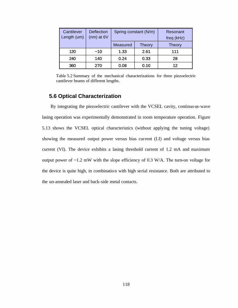
118
270
140
~10
Deflection (nm) at 6V
120.100.08360
280.330.24240
1112.611.33120
TheoryTheoryMeasured
Resonant freq (kHz)
Spring constant (N/m)Cantilever Length (um)
270
140
~10
Deflection (nm) at 6V
120.100.08360
280.330.24240
1112.611.33120
TheoryTheoryMeasured
Resonant freq (kHz)
Spring constant (N/m)Cantilever Length (um)
Table 5.2 Summary of the mechanical characterizations for three piezoelectric cantilever beams of different lengths.
5.6 Optical Characterization
By integrating the piezoelectric cantilever with the VCSEL cavity, continuous-wave
lasing operation was experimentally demonstrated in room temperature operation. Figure
5.13 shows the VCSEL optical characteristics (without applying the tuning voltage)
showing the measured output power versus bias current (LI) and voltage versus bias
current (VI). The device exhibits a lasing threshold current of 1.2 mA and maximum
output power of ~1.2 mW with the slope efficiency of 0.3 W/A. The turn-on voltage for
the device is quite high, in combination with high serial resistance. Both are attributed to
the un-annealed laser and back-side metal contacts.
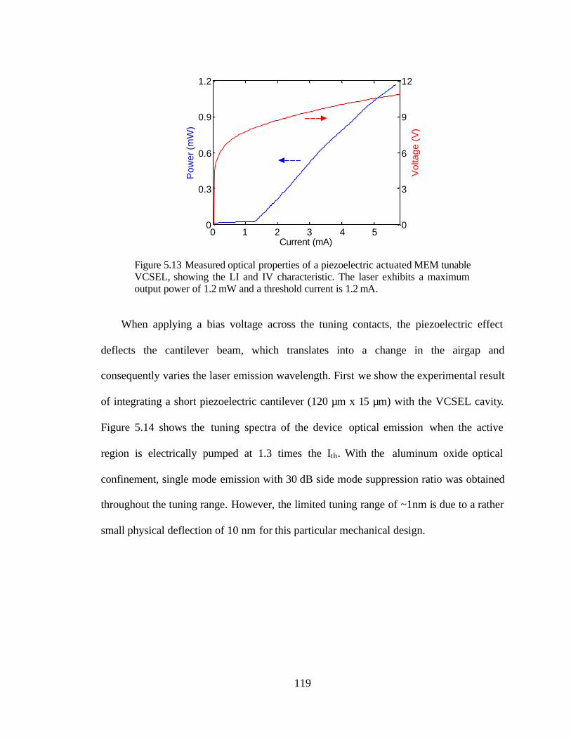
119
0 1 2 3 4 50
0.3
0.6
0.9
1.2
Current (mA)
Pow
er (m
W)
0
3
6
9
12
Vol
tage
(V
)
Figure 5.13 Measured optical properties of a piezoelectric actuated MEM tunable VCSEL, showing the LI and IV characteristic. The laser exhibits a maximum output power of 1.2 mW and a threshold current is 1.2 mA.
When applying a bias voltage across the tuning contacts, the piezoelectric effect
deflects the cantilever beam, which translates into a change in the airgap and
consequently varies the laser emission wavelength. First we show the experimental result
of integrating a short piezoelectric cantilever (120 µm x 15 µm) with the VCSEL cavity.
Figure 5.14 shows the tuning spectra of the device optical emission when the active
region is electrically pumped at 1.3 times the Ith. With the aluminum oxide optical
confinement, single mode emission with 30 dB side mode suppression ratio was obtained
throughout the tuning range. However, the limited tuning range of ~1nm is due to a rather
small physical deflection of 10 nm for this particular mechanical design.
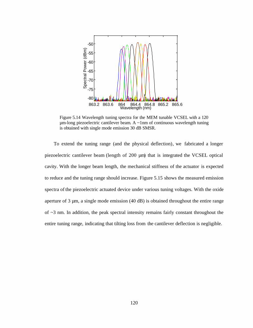
120
863.2 863.6 864 864.4 864.8 865.2 865.6-80
-75
-70
-65
-60
-55
-50
Wavelength (nm)
Spe
ctra
l Pow
er (
dBm
)
Figure 5.14 Wavelength tuning spectra for the MEM tunable VCSEL with a 120 µm-long piezoelectric cantilever beam. A ~1nm of continuous wavelength tuning is obtained with single mode emission 30 dB SMSR.
To extend the tuning range (and the physical deflection), we fabricated a longer
piezoelectric cantilever beam (length of 200 µm) that is integrated the VCSEL optical
cavity. With the longer beam length, the mechanical stiffness of the actuator is expected
to reduce and the tuning range should increase. Figure 5.15 shows the measured emission
spectra of the piezoelectric actuated device under various tuning voltages. With the oxide
aperture of 3 µm, a single mode emission (40 dB) is obtained throughout the entire range
of ~3 nm. In addition, the peak spectral intensity remains fairly constant throughout the
entire tuning range, indicating that tilting loss from the cantilever deflection is negligible.
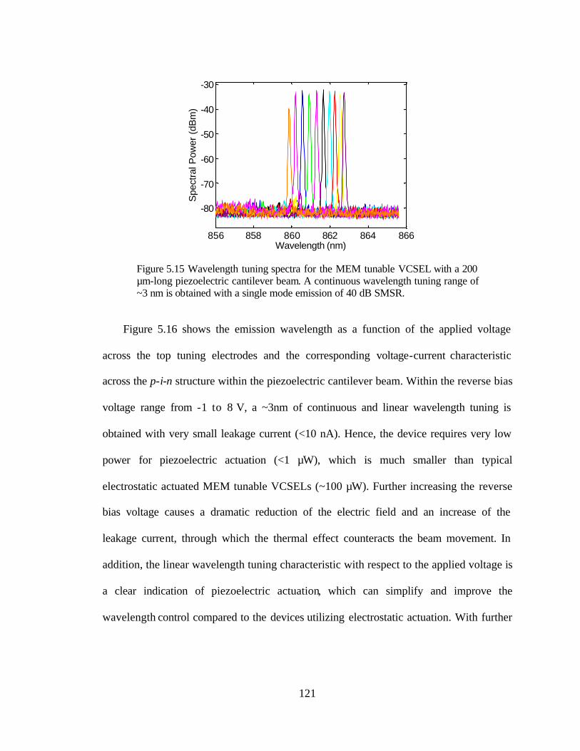
121
856 858 860 862 864 866
-80
-70
-60
-50
-40
-30
Wavelength (nm)
Spe
ctra
l Pow
er (
dBm
)
Figure 5.15 Wavelength tuning spectra for the MEM tunable VCSEL with a 200 µm-long piezoelectric cantilever beam. A continuous wavelength tuning range of ~3 nm is obtained with a single mode emission of 40 dB SMSR.
Figure 5.16 shows the emission wavelength as a function of the applied voltage
across the top tuning electrodes and the corresponding voltage-current characteristic
across the p-i-n structure within the piezoelectric cantilever beam. Within the reverse bias
voltage range from -1 to 8 V, a ~3nm of continuous and linear wavelength tuning is
obtained with very small leakage current (<10 nA). Hence, the device requires very low
power for piezoelectric actuation (<1 µW), which is much smaller than typical
electrostatic actuated MEM tunable VCSELs (~100 µW). Further increasing the reverse
bias voltage causes a dramatic reduction of the electric field and an increase of the
leakage current, through which the thermal effect counteracts the beam movement. In
addition, the linear wavelength tuning characteristic with respect to the applied voltage is
a clear indication of piezoelectric actuation, which can simplify and improve the
wavelength control compared to the devices utilizing electrostatic actuation. With further
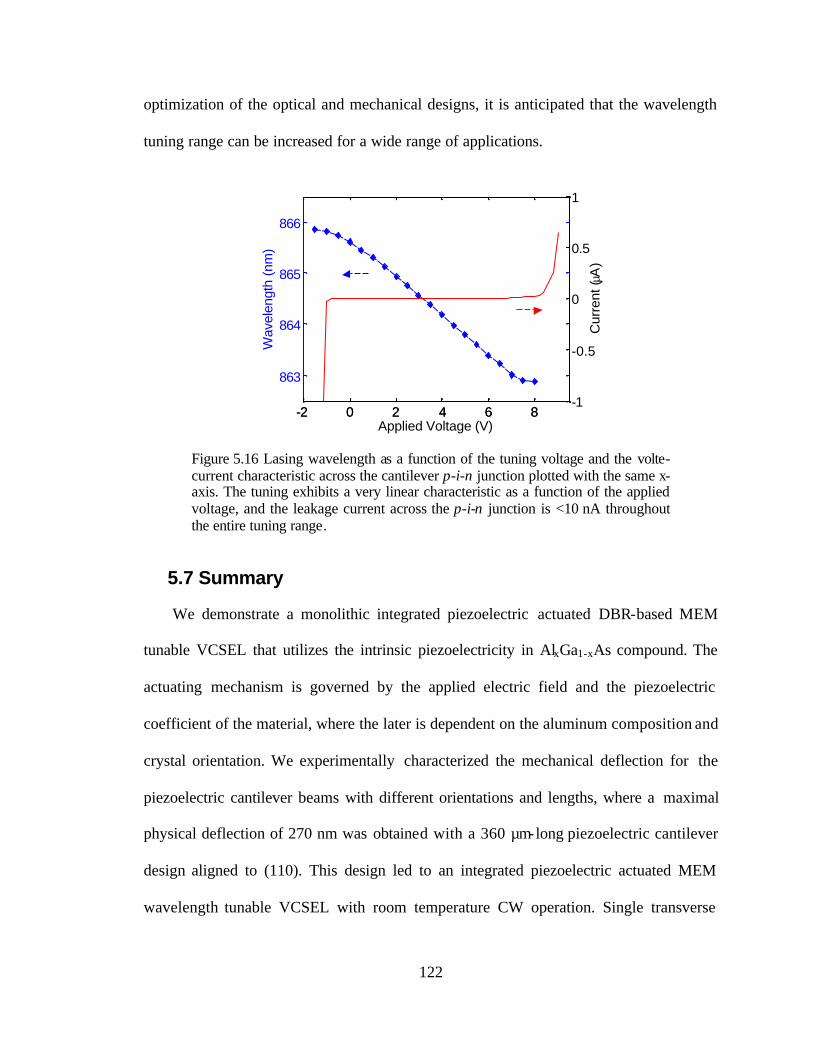
122
optimization of the optical and mechanical designs, it is anticipated that the wavelength
tuning range can be increased for a wide range of applications.
-2 0 2 4 6 8
866
865
864
863
Applied Voltage (V)
Wav
elen
gth
(nm
)
-2 0 2 4 6 8-1
-0.5
0
0.5
1
Cur
rent
(µA
)
Figure 5.16 Lasing wavelength as a function of the tuning voltage and the volte-current characteristic across the cantilever p-i-n junction plotted with the same x-axis. The tuning exhibits a very linear characteristic as a function of the applied voltage, and the leakage current across the p-i-n junction is <10 nA throughout the entire tuning range.
5.7 Summary
We demonstrate a monolithic integrated piezoelectric actuated DBR-based MEM
tunable VCSEL that utilizes the intrinsic piezoelectricity in AlxGa1-xAs compound. The
actuating mechanism is governed by the applied electric field and the piezoelectric
coefficient of the material, where the later is dependent on the aluminum composition and
crystal orientation. We experimentally characterized the mechanical deflection for the
piezoelectric cantilever beams with different orientations and lengths, where a maximal
physical deflection of 270 nm was obtained with a 360 µm-long piezoelectric cantilever
design aligned to (110). This design led to an integrated piezoelectric actuated MEM
wavelength tunable VCSEL with room temperature CW operation. Single transverse
123
mode emission (40 dB) with linear, continuous wavelength tuning of ~3 nm was obtained
for an 850 nm VCSEL with output power of 1.2 mW.
In short, mechanically tunable VCSELs and photonic devices can benefit
tremendously by using piezoelectric actuation. It consumes very low power dissipation
and can eliminate the possibility of catastrophic damage created by pull- in effects known
for electrostatic actuated devices. In addition, it can potentially offer a large, bi-
directional tuning range and is highly promising for many tunable MEM or NEM
optoelectronic device implementations.
124
Chapter 6 VCSEL Optoelectronic Biosensor
6.1 Motivation
Rapid detection of infectious diseases is indispensable for diagnosing patients and
directing public health decisions, especially for developing countries. It often requires
sensitive tools that can detect and quantify interactions of various biomolecular
pathogens. The priorities for point-of-care diagnostics are rapidity, ease-of use and low
cost, while maintaining the required clinical sensitivity. But, most of the current
technologies largely fail to address the needs specific to point-of-care clinical settings.
Enzyme-linked immunosorbent assay (ELISA) is the predominant immunological
diagnostic assay technology used in most clinical settings. Typical ELISA performs
sufficiently to address a broad range of clinical diagnostic needs. However, the ELISA
platform requires laboratory facilities and equipment that are restrictive for point-of-care
diagnostics. Also, the standard ELISA procedures require tedious sample preparation
from the numerous incubation and liquid dispensing-washing steps. The quantification
125
process requires a spectrophotometer that is not available in a low-cost, mobile platform.
Furthermore, a colorimetric label is required to be attached to the molecules under study,
which may substantially increase the assay complexity and potentially alter the
functionality of molecules. In this chapter, we present a novel label- free biosensor based
on a tunable VCSEL.
6.2 Label Free Biosensor
Bioassays are important tools used to detect interactions of various biomolecular
complexes for pharmaceutical and biomedical applications. In addition, such analysis
methods can provide a deep understanding on how proteins, as encoded by DNA, interact
with enzymes, inhibitors or other proteins. This is one of the most important next grand
challenges after the completion of the sequencing of the human genome.
In general, bioassay techniques can be put into two categories: labeling with
compounds (fluorescent, radioactive or colorimetric) and direct molecule identification.
For the majority of bioassays currently performed for life science research and
pharmaceutical drug screening, fluorescent or colorimetric chemical labels are commonly
attached to the molecules under study, as shown in Figure 6.1(a). Labels can be readily
visualized and the measurement techniques are simple. However, the attachment of
labels may substantially increase the assay complexity and sample preparation time. It
may also alter the functionality of molecules through conformational modification or
epitope blocking, which ultimately causes errors in the final data interpretation.
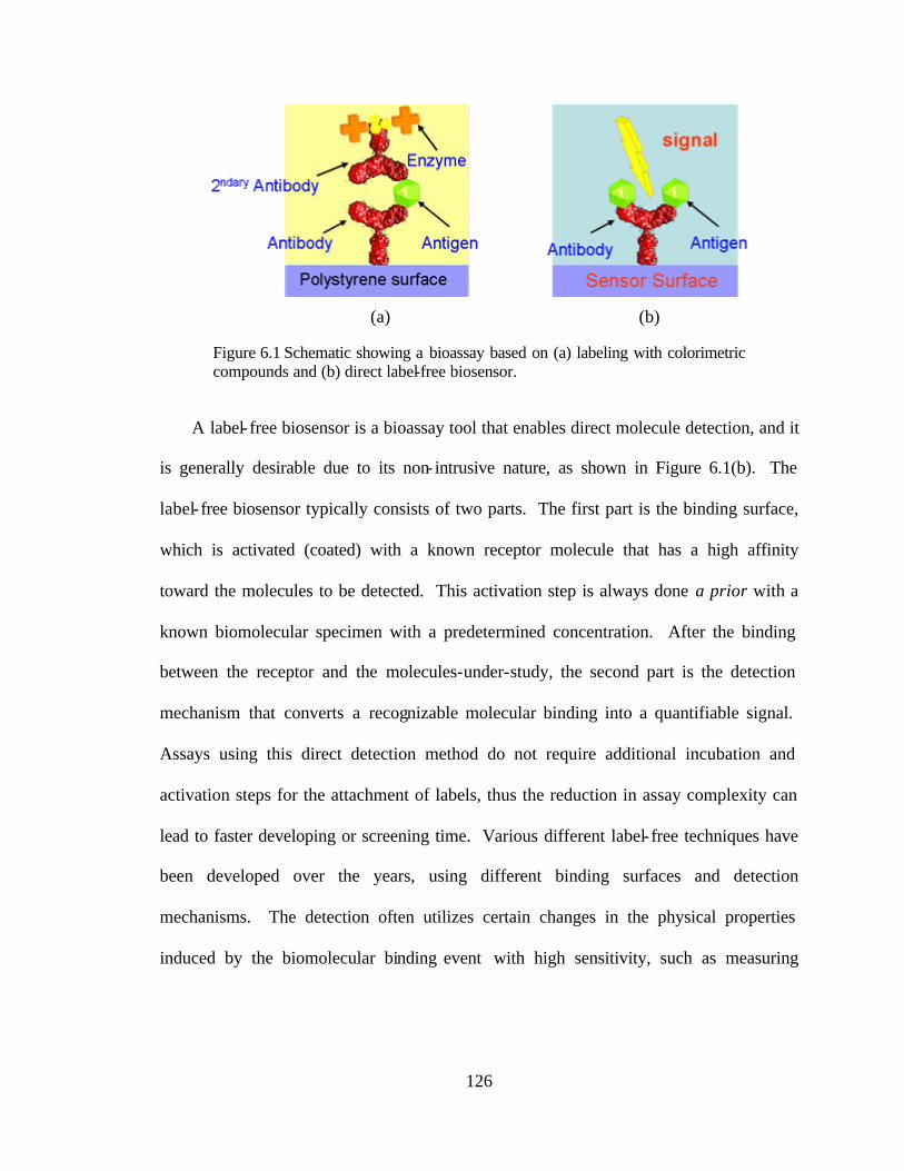
126
(a) (b)
Figure 6.1 Schematic showing a bioassay based on (a) labeling with colorimetric compounds and (b) direct label-free biosensor.
A label- free biosensor is a bioassay tool that enables direct molecule detection, and it
is generally desirable due to its non- intrusive nature, as shown in Figure 6.1(b). The
label- free biosensor typically consists of two parts. The first part is the binding surface,
which is activated (coated) with a known receptor molecule that has a high affinity
toward the molecules to be detected. This activation step is always done a prior with a
known biomolecular specimen with a predetermined concentration. After the binding
between the receptor and the molecules-under-study, the second part is the detection
mechanism that converts a recognizable molecular binding into a quantifiable signal.
Assays using this direct detection method do not require additional incubation and
activation steps for the attachment of labels, thus the reduction in assay complexity can
lead to faster developing or screening time. Various different label- free techniques have
been developed over the years, using different binding surfaces and detection
mechanisms. The detection often utilizes certain changes in the physical properties
induced by the biomolecular binding event with high sensitivity, such as measuring
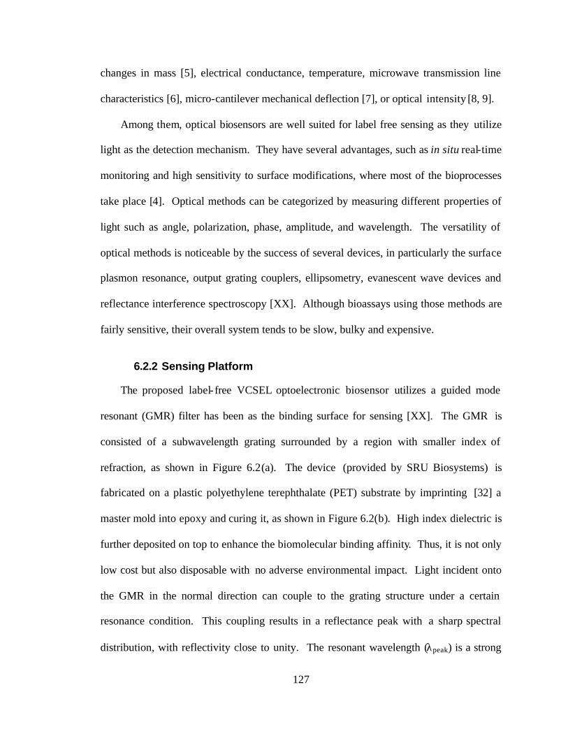
127
changes in mass [5], electrical conductance, temperature, microwave transmission line
characteristics [6], micro-cantilever mechanical deflection [7], or optical intensity [8, 9].
Among them, optical biosensors are well suited for label free sensing as they utilize
light as the detection mechanism. They have several advantages, such as in situ real-time
monitoring and high sensitivity to surface modifications, where most of the bioprocesses
take place [4]. Optical methods can be categorized by measuring different properties of
light such as angle, polarization, phase, amplitude, and wavelength. The versatility of
optical methods is noticeable by the success of several devices, in particularly the surface
plasmon resonance, output grating couplers, ellipsometry, evanescent wave devices and
reflectance interference spectroscopy [XX]. Although bioassays using those methods are
fairly sensitive, their overall system tends to be slow, bulky and expensive.
6.2.2 Sensing Platform
The proposed label- free VCSEL optoelectronic biosensor utilizes a guided mode
resonant (GMR) filter has been as the binding surface for sensing [XX]. The GMR is
consisted of a subwavelength grating surrounded by a region with smaller index of
refraction, as shown in Figure 6.2(a). The device (provided by SRU Biosystems) is
fabricated on a plastic polyethylene terephthalate (PET) substrate by imprinting [32] a
master mold into epoxy and curing it, as shown in Figure 6.2(b). High index dielectric is
further deposited on top to enhance the biomolecular binding affinity. Thus, it is not only
low cost but also disposable with no adverse environmental impact. Light incident onto
the GMR in the normal direction can couple to the grating structure under a certain
resonance condition. This coupling results in a reflectance peak with a sharp spectral
distribution, with reflectivity close to unity. The resonant wavelength (λpeak) is a strong
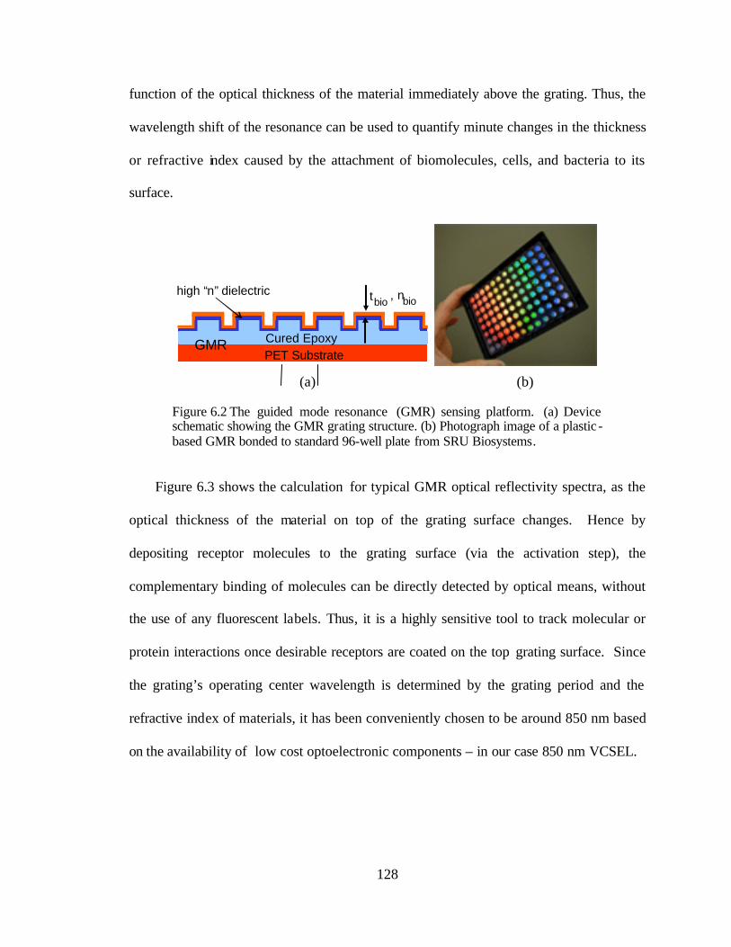
128
function of the optical thickness of the material immediately above the grating. Thus, the
wavelength shift of the resonance can be used to quantify minute changes in the thickness
or refractive index caused by the attachment of biomolecules, cells, and bacteria to its
surface.
PET SubstrateCured Epoxy
high “n”dielectricbiobio , nt
GMR
(a) (b)
Figure 6.2 The guided mode resonance (GMR) sensing platform. (a) Device schematic showing the GMR grating structure. (b) Photograph image of a plastic -based GMR bonded to standard 96-well plate from SRU Biosystems.
Figure 6.3 shows the calculation for typical GMR optical reflectivity spectra, as the
optical thickness of the material on top of the grating surface changes. Hence by
depositing receptor molecules to the grating surface (via the activation step), the
complementary binding of molecules can be directly detected by optical means, without
the use of any fluorescent labels. Thus, it is a highly sensitive tool to track molecular or
protein interactions once desirable receptors are coated on the top grating surface. Since
the grating’s operating center wavelength is determined by the grating period and the
refractive index of materials, it has been conveniently chosen to be around 850 nm based
on the availability of low cost optoelectronic components – in our case 850 nm VCSEL.
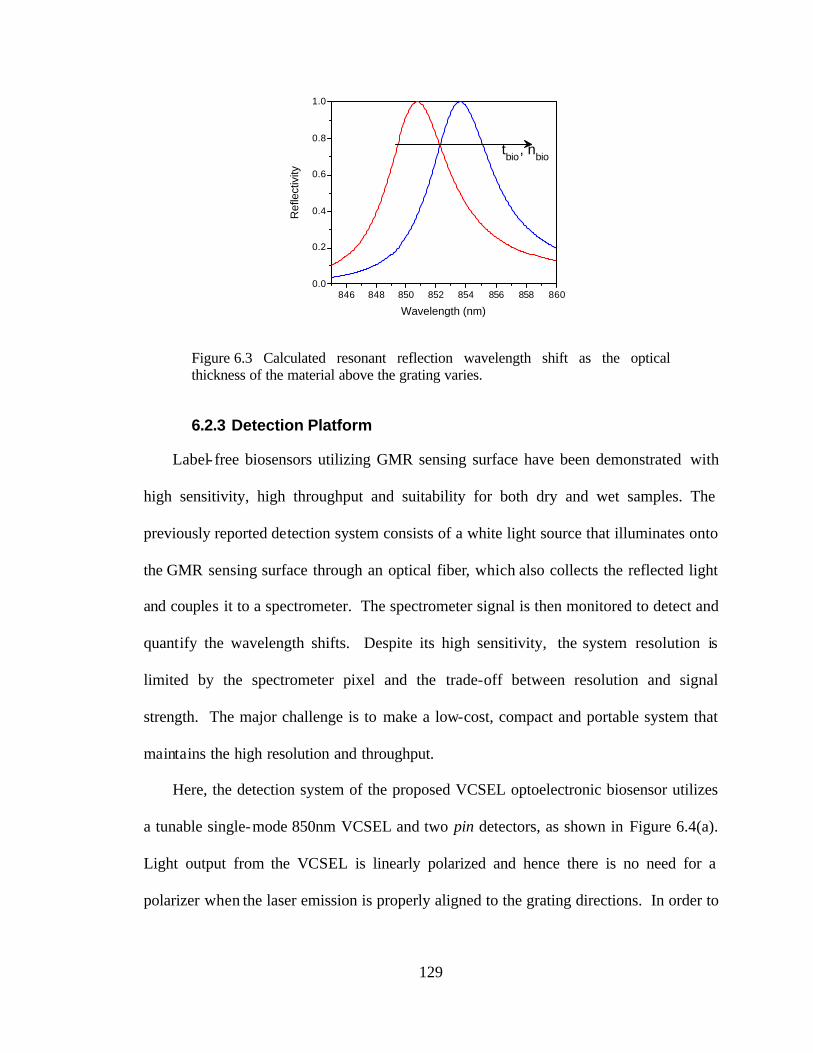
129
846 848 850 852 854 856 858 8600.0
0.2
0.4
0.6
0.8
1.0
Ref
lect
ivity
Wavelength (nm)
tbio, nbio
Figure 6.3 Calculated resonant reflection wavelength shift as the optical thickness of the material above the grating varies.
6.2.3 Detection Platform
Label- free biosensors utilizing GMR sensing surface have been demonstrated with
high sensitivity, high throughput and suitability for both dry and wet samples. The
previously reported detection system consists of a white light source that illuminates onto
the GMR sensing surface through an optical fiber, which also collects the reflected light
and couples it to a spectrometer. The spectrometer signal is then monitored to detect and
quantify the wavelength shifts. Despite its high sensitivity, the system resolution is
limited by the spectrometer pixel and the trade-off between resolution and signal
strength. The major challenge is to make a low-cost, compact and portable system that
maintains the high resolution and throughput.
Here, the detection system of the proposed VCSEL optoelectronic biosensor utilizes
a tunable single-mode 850nm VCSEL and two pin detectors, as shown in Figure 6.4(a).
Light output from the VCSEL is linearly polarized and hence there is no need for a
polarizer when the laser emission is properly aligned to the grating directions. In order to
130
scan for the peak resonant position λpeak, the VCSEL wavelength is tuned by sweeping its
bias current, causing a rapid thermal effect that shifts the lasing wavelength. Detector 1
is positioned to measure the reflected light from the GMR substrate, while detector 2
provides the normalization for the incident power, since the VCSEL output power also
varies with the bias current. Thus, the ratio of the two detector signals is used to monitor
the reflection peak, as shown in Figure 6.4(b). The periodic raw signal measured
originates from the optical reflection present in the setup, which can be removed by
numerical methods (blue line) and curve fitted (red line). Varying the laser bias current
provides a fast but narrow wavelength tuning range 2−3 nm) for the VCSEL. As shown
in Figure 6.4(b), the laser wavelength shifts from 852.5 to 855.5 nm as the bias current
increases from 2 to 9 mA. Temperature tuning is also used to augment the tuning range,
extending it to 8−9 nm. This is primarily used to ensure the GMR resonant spectral peak
is within the 3 nm wavelength range obtained by sweeping the laser’s current. During the
operation, laser bias current is kept below its roll-off bias (9 mA), assuring single-mode
operation for the VCSEL with a 5-7º beam divergence angle. The typical wavelength
dependence for temperature and current tuning for a VCSEL is 0.08nm/ºC and
0.4nm/mA, respectively. In this proof-of-concept demonstration, a commercial single-
mode 850 nm implant-VCSEL in TO-can packaged was used. But for biomolecular or
cellular interactions that require a larger system dynamic range, a larger wavelength
tunable light source can be obtained by using a MEM tunable VCSEL.
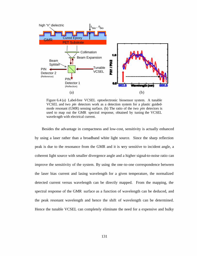
131
PIN Detector 2(Reference)
Beam Expansion
Collimation
Tunable VCSEL
PET Substrate
Beam Splitter
PIN Detector 1 (Reflection)
Cured Epoxy
high “n”dielectricbiobio , nt
GMR
(a) (b)
Figure 6.4 (a) Label-free VCSEL optoelectronic biosensor system. A tunable VCSEL and two pin detectors work as a detection system for a plastic guided-mode resonant (GMR) sensing surface. (b) The ratio of the two pin detectors is used to map out the GMR spectral response, obtained by tuning the VCSEL wavelength with electrical current.
Besides the advantage in compactness and low-cost, sensitivity is actually enhanced
by using a laser rather than a broadband white light source. Since the sharp reflection
peak is due to the resonance from the GMR and it is very sensitive to incident angle, a
coherent light source with smaller divergence angle and a higher signal-to-noise ratio can
improve the sensitivity of the system. By using the one-to-one correspondence between
the laser bias current and lasing wavelength for a given temperature, the normalized
detected current versus wavelength can be directly mapped. From the mapping, the
spectral response of the GMR surface as a function of wavelength can be deduced, and
the peak resonant wavelength and hence the shift of wavelength can be determined.
Hence the tunable VCSEL can completely eliminate the need for a expensive and bulky
132
spectrometer. Moreover, the electrical circuit board (for signal processing and driving
the VCSEL detector) and optical assembly can be packaged into a compact form factor.
6.3 Antibody-Antigen Assay
The application of the VCSEL based label- free biosensor measurement system for
protein-protein binding immunoassays was investigated. The characterization of protein
interactions consists of the detection of the binding between antibodies: goat anti-mouse
immunoglobulin (IgG), and antigens: mouse immunoglobulin (IgG). The proteins were
obtained from Jackson ImmunoResearch, each being affinity-purified and
chromatography-purified, respectively. Three different experiments were performed, in
order to study the performance of the biosensor system: ELISA, dynamic real-time
binding monitoring and static concentration measurements. The dynamic experiment
enables the quantification of the antibody-antigen binding as a function of time.
Meanwhile, the static experiment quantifies the resonant wavelength shift as a function of
mouse IgG concentration.
6.3.1 Experimental Procedure
The protocol for all three experiments followed a standard mouse IgG capture
immunoassay, as shown in Figure 6.5. First, the antibody protein was deposited by
applying 100µl/well of goat anti-mouse IgG (1.8µg/ml), which was diluted in phosphate-
buffered saline (PBS) solution, and it was incubated for 10-12 hours at 4ºC. The
incubation period allowed sufficient time for the mouse IgG protein to bind to the GMR
sensor surface and the low temperature favors the binding. Then the excess solution was
removed and the wells were washed with PBS-Tween. Next, normal goat serum
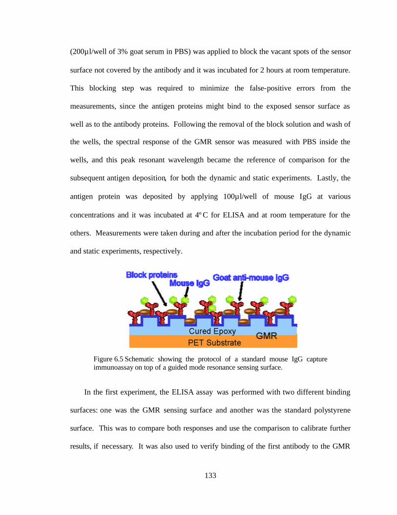
133
(200µl/well of 3% goat serum in PBS) was applied to block the vacant spots of the sensor
surface not covered by the antibody and it was incubated for 2 hours at room temperature.
This blocking step was required to minimize the false-positive errors from the
measurements, since the antigen proteins might bind to the exposed sensor surface as
well as to the antibody proteins. Following the removal of the block solution and wash of
the wells, the spectral response of the GMR sensor was measured with PBS inside the
wells, and this peak resonant wavelength became the reference of comparison for the
subsequent antigen deposition, for both the dynamic and static experiments. Lastly, the
antigen protein was deposited by applying 100µl/well of mouse IgG at various
concentrations and it was incubated at 4ºC for ELISA and at room temperature for the
others. Measurements were taken during and after the incubation period for the dynamic
and static experiments, respectively.
Figure 6.5 Schematic showing the protocol of a standard mouse IgG capture immunoassay on top of a guided mode resonance sensing surface.
In the first experiment, the ELISA assay was performed with two different binding
surfaces: one was the GMR sensing surface and another was the standard polystyrene
surface. This was to compare both responses and use the comparison to calibrate further
results, if necessary. It was also used to verify binding of the first antibody to the GMR
134
surface and test the surface activation. ELISA required two additional steps than those
described above and the protocol also required that mouse IgG (antigen) is incubated for
10-12 hours at 4ºC. The additional required steps were a second antibody (which has the
labels) incubation and development of the labels. This second labeled antibody
incubation was done after removing and washing the previous solution that had antigen,
and it specifically binds to the antigen. More than one binding per antigen may occur,
resulting in amplification. This double antibody binding is also called sandwich ELISA.
The label of the secondary antibody, usually an enzyme, converts the colorless substrate
to a colored product. In this case, the enzyme is p-nitrophenyl-phosphate (pNPP) which
is converted to the yellow p-nitrophenol by alkaline phosphatase. This colored product is
measured on an ELISA plate reader as function of the optical density at some specific
wavelength, in this case yellow.
Figure 6.6 shows optical density at λ = 560nm measured by the ELISA spectrometer
for both GMR and standard polystyrene ELISA plate. The result from the GMR plate has
higher sensitivity than the polystyrene plate as seen from the larger range of optical
density. However, it also has a strong background noise due to interference of the grating
with the read out system. The results shown were normalized with respect to the
background for both plates. The nearly similar response for the two plates shows that
further calibration of the GMR results is not necessary.
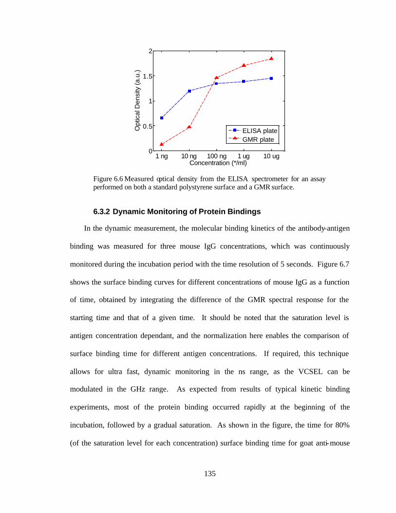
135
1 ng 10 ng 100 ng 1 ug 10 ug0
0.5
1
1.5
2
Concentration (*/ml)
Opt
ical
Den
sity
(a.u
.)ELISA plateGMR plate
Figure 6.6 Measured optical density from the ELISA spectrometer for an assay performed on both a standard polystyrene surface and a GMR surface.
6.3.2 Dynamic Monitoring of Protein Bindings
In the dynamic measurement, the molecular binding kinetics of the antibody-antigen
binding was measured for three mouse IgG concentrations, which was continuously
monitored during the incubation period with the time resolution of 5 seconds. Figure 6.7
shows the surface binding curves for different concentrations of mouse IgG as a function
of time, obtained by integrating the difference of the GMR spectral response for the
starting time and that of a given time. It should be noted that the saturation level is
antigen concentration dependant, and the normalization here enables the comparison of
surface binding time for different antigen concentrations. If required, this technique
allows for ultra fast, dynamic monitoring in the ns range, as the VCSEL can be
modulated in the GHz range. As expected from results of typical kinetic binding
experiments, most of the protein binding occurred rapidly at the beginning of the
incubation, followed by a gradual saturation. As shown in the figure, the time for 80%
(of the saturation level for each concentration) surface binding time for goat anti-mouse
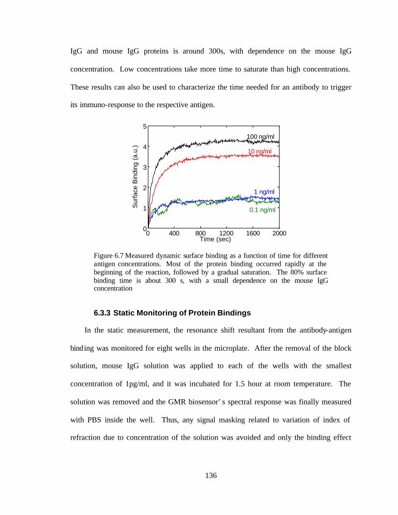
136
IgG and mouse IgG proteins is around 300s, with dependence on the mouse IgG
concentration. Low concentrations take more time to saturate than high concentrations.
These results can also be used to characterize the time needed for an antibody to trigger
its immuno-response to the respective antigen.
0 400 800 1200 1600 20000
1
2
3
4
5
Time (sec)
Sur
face
Bin
ding
(a.
u.)
100 ng/ml
10 ng/ml
1 ng/ml
0.1 ng/ml
Figure 6.7 Measured dynamic surface binding as a function of time for different antigen concentrations. Most of the protein binding occurred rapidly at the beginning of the reaction, followed by a gradual saturation. The 80% surface binding time is about 300 s, with a small dependence on the mouse IgG concentration
6.3.3 Static Monitoring of Protein Bindings
In the static measurement, the resonance shift resultant from the antibody-antigen
binding was monitored for eight wells in the microplate. After the removal of the block
solution, mouse IgG solution was applied to each of the wells with the smallest
concentration of 1pg/ml, and it was incubated for 1.5 hour at room temperature. The
solution was removed and the GMR biosensor’s spectral response was finally measured
with PBS inside the well. Thus, any signal masking related to variation of index of
refraction due to concentration of the solution was avoided and only the binding effect
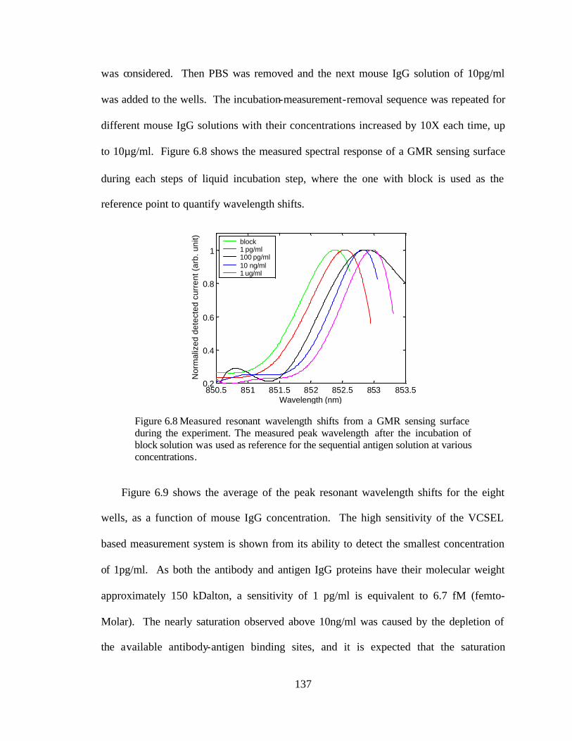
137
was considered. Then PBS was removed and the next mouse IgG solution of 10pg/ml
was added to the wells. The incubation-measurement-removal sequence was repeated for
different mouse IgG solutions with their concentrations increased by 10X each time, up
to 10µg/ml. Figure 6.8 shows the measured spectral response of a GMR sensing surface
during each steps of liquid incubation step, where the one with block is used as the
reference point to quantify wavelength shifts.
850.5 851 851.5 852 852.5 853 853.50.2
0.4
0.6
0.8
1
Wavelength (nm)
Nor
mal
ized
det
ecte
d cu
rren
t (ar
b. u
nit)
well 66
block1 pg/ml100 pg/ml10 ng/ml1 ug/ml
Figure 6.8 Measured resonant wavelength shifts from a GMR sensing surface during the experiment. The measured peak wavelength after the incubation of block solution was used as reference for the sequential antigen solution at various concentrations.
Figure 6.9 shows the average of the peak resonant wavelength shifts for the eight
wells, as a function of mouse IgG concentration. The high sensitivity of the VCSEL
based measurement system is shown from its ability to detect the smallest concentration
of 1pg/ml. As both the antibody and antigen IgG proteins have their molecular weight
approximately 150 kDalton, a sensitivity of 1 pg/ml is equivalent to 6.7 fM (femto-
Molar). The nearly saturation observed above 10ng/ml was caused by the depletion of
the available antibody-antigen binding sites, and it is expected that the saturation
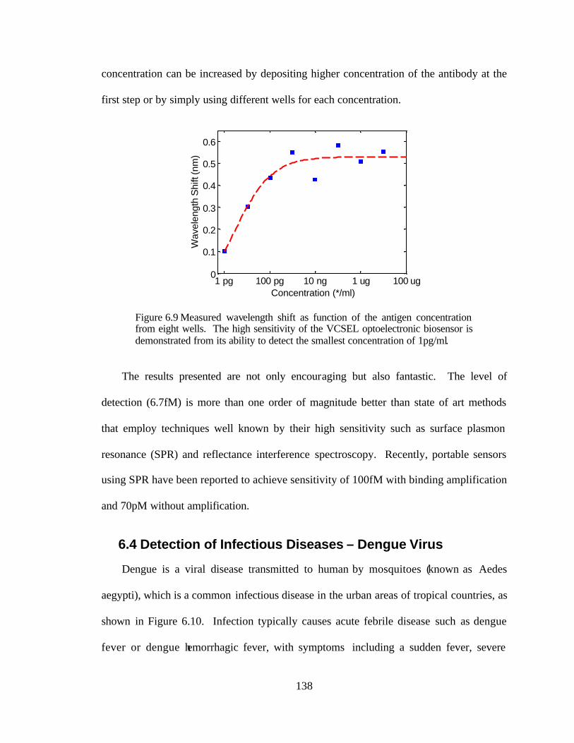
138
concentration can be increased by depositing higher concentration of the antibody at the
first step or by simply using different wells for each concentration.
1 pg 100 pg 10 ng 1 ug 100 ug0
0.1
0.2
0.3
0.4
0.5
0.6
Concentration (*/ml)
Wav
elen
gth
Shi
ft (n
m)
Figure 6.9 Measured wavelength shift as function of the antigen concentration from eight wells. The high sensitivity of the VCSEL optoelectronic biosensor is demonstrated from its ability to detect the smallest concentration of 1pg/ml.
The results presented are not only encouraging but also fantastic. The level of
detection (6.7fM) is more than one order of magnitude better than state of art methods
that employ techniques well known by their high sensitivity such as surface plasmon
resonance (SPR) and reflectance interference spectroscopy. Recently, portable sensors
using SPR have been reported to achieve sensitivity of 100fM with binding amplification
and 70pM without amplification.
6.4 Detection of Infectious Diseases – Dengue Virus
Dengue is a viral disease transmitted to human by mosquitoes (known as Aedes
aegypti), which is a common infectious disease in the urban areas of tropical countries, as
shown in Figure 6.10. Infection typically causes acute febrile disease such as dengue
fever or dengue hemorrhagic fever, with symptoms including a sudden fever, severe

139
headache, muscle pains, and rashes. Dengue infection is considered as one of the most
important infectious diseases in terms of morbidity and morality. Annual estimate shows
more than one hundred million cases of dengue fever, several hundred thousands cases of
dengue hemorrhagic, and about 2.5 billion people at risk for the infection.
Figure 6.10 Image of the Aedes aegypti mosquito that transmits dengue virus to human. (b) Illustration of world-side dengue infection distribution in 2000.
Since dengue has a rather short incubation period in the human body – often just a
few days, a sensitive and high-throughput diagnosis tool is required to detect the
epidemic disease for early treatment. Figure 6.11 shows the human’s body temperature
and anti-dengue antibodies (IgM) concentration as a function of days after dengue
infection. A highly sensitive biosensor is especially important since the concentration of
IgM only becomes substantially detectable after 4-5 days post the infection. In this
section, we present the application of the VCSEL optoelectronic biosensor for the
detection of this infectious disease from human serum samples, specifically the
interactions of human antibodies against dengue viral antigens. This is a realistic test for
the performance of the label- free biosensor in a clinical relevant assay, since human
serum contains various interfering proteins such as albumin and other immunoglobulins
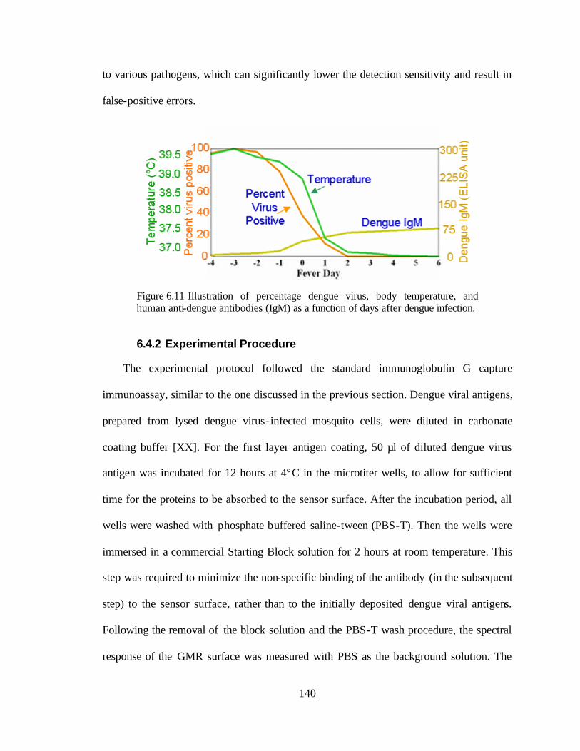
140
to various pathogens, which can significantly lower the detection sensitivity and result in
false-positive errors.
Figure 6.11 Illustration of percentage dengue virus, body temperature, and human anti-dengue antibodies (IgM) as a function of days after dengue infection.
6.4.2 Experimental Procedure
The experimental protocol followed the standard immunoglobulin G capture
immunoassay, similar to the one discussed in the previous section. Dengue viral antigens,
prepared from lysed dengue virus- infected mosquito cells, were diluted in carbonate
coating buffer [XX]. For the first layer antigen coating, 50 µl of diluted dengue virus
antigen was incubated for 12 hours at 4°C in the microtiter wells, to allow for sufficient
time for the proteins to be absorbed to the sensor surface. After the incubation period, all
wells were washed with phosphate buffered saline-tween (PBS-T). Then the wells were
immersed in a commercial Starting Block solution for 2 hours at room temperature. This
step was required to minimize the non-specific binding of the antibody (in the subsequent
step) to the sensor surface, rather than to the initially deposited dengue viral antigens.
Following the removal of the block solution and the PBS-T wash procedure, the spectral
response of the GMR surface was measured with PBS as the background solution. The
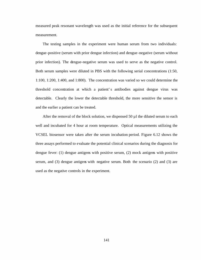
141
measured peak resonant wavelength was used as the initial reference for the subsequent
measurement.
The testing samples in the experiment were human serum from two individuals:
dengue-positive (serum with prior dengue infection) and dengue-negative (serum without
prior infection). The dengue-negative serum was used to serve as the negative control.
Both serum samples were diluted in PBS with the following serial concentrations (1:50,
1:100, 1:200, 1:400, and 1:800). The concentration was varied so we could determine the
threshold concentration at which a patient’s antibodies against dengue virus was
detectable. Clearly the lower the detectable threshold, the more sensitive the sensor is
and the earlier a patient can be treated.
After the removal of the block solution, we dispensed 50 µ l the diluted serum to each
well and incubated for 4 hour at room temperature. Optical measurements utilizing the
VCSEL biosensor were taken after the serum incubation period. Figure 6.12 shows the
three assays performed to evaluate the potential clinical scenarios during the diagnosis for
dengue fever: (1) dengue antigens with positive serum, (2) mock antigens with positive
serum, and (3) dengue antigens with negative serum. Both the scenario (2) and (3) are
used as the negative controls in the experiment.
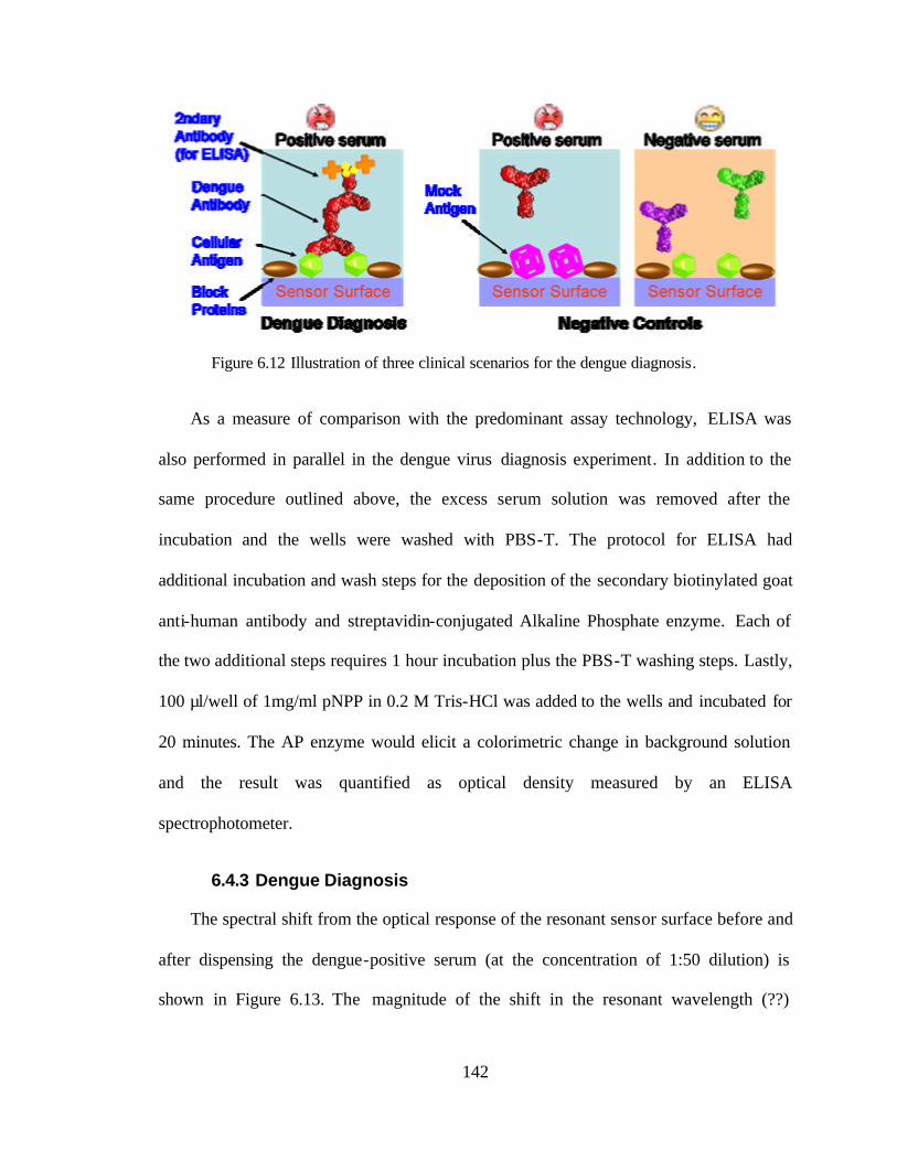
142
Figure 6.12 Illustration of three clinical scenarios for the dengue diagnosis.
As a measure of comparison with the predominant assay technology, ELISA was
also performed in parallel in the dengue virus diagnosis experiment. In addition to the
same procedure outlined above, the excess serum solution was removed after the
incubation and the wells were washed with PBS-T. The protocol for ELISA had
additional incubation and wash steps for the deposition of the secondary biotinylated goat
anti-human antibody and streptavidin-conjugated Alkaline Phosphate enzyme. Each of
the two additional steps requires 1 hour incubation plus the PBS-T washing steps. Lastly,
100 µl/well of 1mg/ml pNPP in 0.2 M Tris-HCl was added to the wells and incubated for
20 minutes. The AP enzyme would elicit a colorimetric change in background solution
and the result was quantified as optical density measured by an ELISA
spectrophotometer.
6.4.3 Dengue Diagnosis
The spectral shift from the optical response of the resonant sensor surface before and
after dispensing the dengue-positive serum (at the concentration of 1:50 dilution) is
shown in Figure 6.13. The magnitude of the shift in the resonant wavelength (??)
143
quantifies the optical thickness change induced by the interactions between the first- layer
coated dengue viral antigens and the human anti-dengue antibodies from the dengue-
positive serum sample. The raw experimental data contains periodic oscillations
originates from the optical reflections within the measurement system, which can be
minimized with proper anti- reflection coatings. In our case, the periodic oscillation in the
data is removed by numerical methods, and the peak resonant wavelength can be more
accurately obtained.
852 853 854 855 8560.2
0.3
0.4
0.5
0.6
Wavelength (nm)
Ref
lect
ed P
ower
(a.
u.)
??
852 853 854 855 8560.2
0.3
0.4
0.5
0.6
Wavelength (nm)
Ref
lect
ed P
ower
(a.
u.)
??
Figure 6.13 Spectral shift from the guided-mode resonance of the surface photonic crystal sensing surface before and after dispensing the dengue-positive serum. The magnitude of the shift (??) quantifies the optical thickness change induced by the biomolecular interactions of dengue virus antigen and human anti-dengue antibody proteins.
In a dengue virus diagnosis to determine if a person was previously infected, we
performed an assay to measure the biomolecular interaction of dengue viral antigens with
both the dengue-positive and dengue-negative serum. The measurement was performed
both using the VCSEL optoelectronic biosensor and ELISA, as shown in Figure 6.14.
The proteins interactions were quantified by the wavelength shifts for the VCSEL
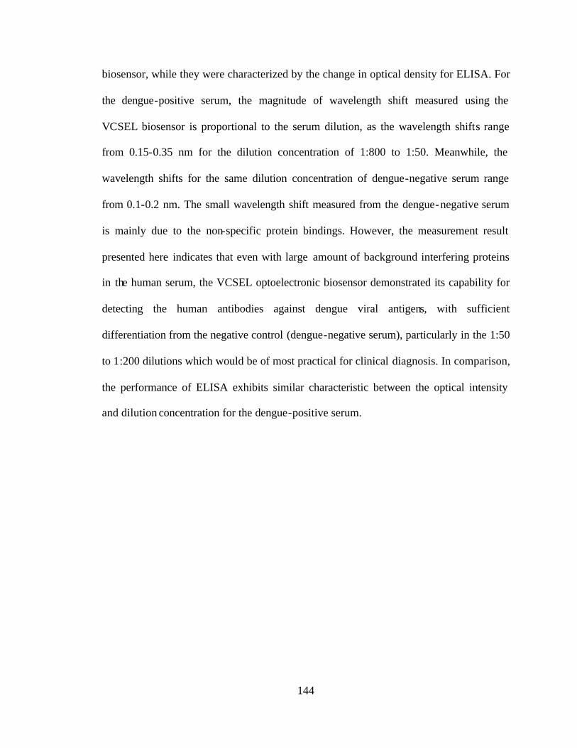
144
biosensor, while they were characterized by the change in optical density for ELISA. For
the dengue-positive serum, the magnitude of wavelength shift measured using the
VCSEL biosensor is proportional to the serum dilution, as the wavelength shifts range
from 0.15-0.35 nm for the dilution concentration of 1:800 to 1:50. Meanwhile, the
wavelength shifts for the same dilution concentration of dengue-negative serum range
from 0.1-0.2 nm. The small wavelength shift measured from the dengue-negative serum
is mainly due to the non-specific protein bindings. However, the measurement result
presented here indicates that even with large amount of background interfering proteins
in the human serum, the VCSEL optoelectronic biosensor demonstrated its capability for
detecting the human antibodies against dengue viral antigens, with sufficient
differentiation from the negative control (dengue-negative serum), particularly in the 1:50
to 1:200 dilutions which would be of most practical for clinical diagnosis. In comparison,
the performance of ELISA exhibits similar characteristic between the optical intensity
and dilution concentration for the dengue-positive serum.
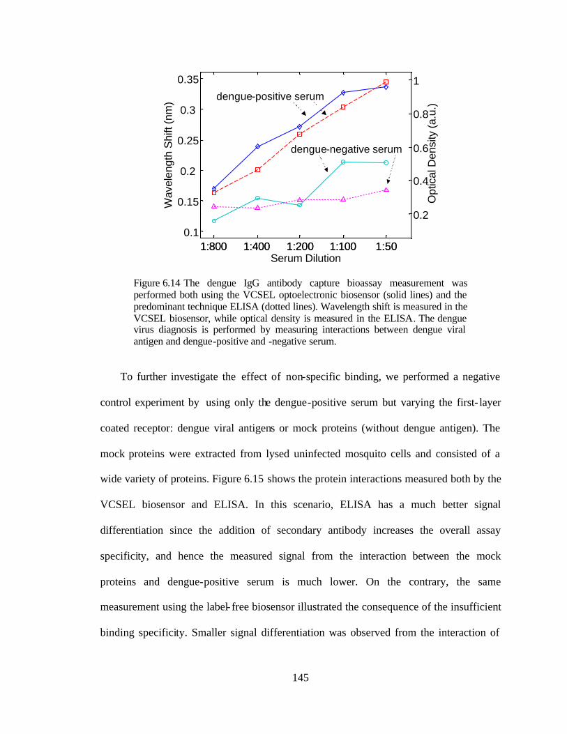
145
1:800 1:400 1:200 1:100 1:500.1
0.15
0.2
0.25
0.3
0.35
Serum Dilution
Wav
elen
gth
Shi
ft (n
m)
1:800 1:400 1:200 1:100 1:50
0.2
0.4
0.6
0.8
1
Opt
ical
Den
sity
(a.u
.)
dengue-positive serum
dengue-negative serum
1:800 1:400 1:200 1:100 1:500.1
0.15
0.2
0.25
0.3
0.35
Serum Dilution
Wav
elen
gth
Shi
ft (n
m)
1:800 1:400 1:200 1:100 1:50
0.2
0.4
0.6
0.8
1
Opt
ical
Den
sity
(a.u
.)
dengue-positive serum
dengue-negative serum
Figure 6.14 The dengue IgG antibody capture bioassay measurement was performed both using the VCSEL optoelectronic biosensor (solid lines) and the predominant technique ELISA (dotted lines). Wavelength shift is measured in the VCSEL biosensor, while optical density is measured in the ELISA. The dengue virus diagnosis is performed by measuring interactions between dengue viral antigen and dengue-positive and -negative serum.
To further investigate the effect of non-specific binding, we performed a negative
control experiment by using only the dengue-positive serum but varying the first- layer
coated receptor: dengue viral antigens or mock proteins (without dengue antigen). The
mock proteins were extracted from lysed uninfected mosquito cells and consisted of a
wide variety of proteins. Figure 6.15 shows the protein interactions measured both by the
VCSEL biosensor and ELISA. In this scenario, ELISA has a much better signal
differentiation since the addition of secondary antibody increases the overall assay
specificity, and hence the measured signal from the interaction between the mock
proteins and dengue-positive serum is much lower. On the contrary, the same
measurement using the label- free biosensor illustrated the consequence of the insufficient
binding specificity. Smaller signal differentiation was observed from the interaction of
146
mock proteins and dengue-positive serum, as compared to that measured from dengue
viral antigens and the dengue-positive serum. This is attributed to the non-specific
bindings from variety of proteins in human serum to mock proteins as well as to the
sensor surface. Although the lack of specificity is an intrinsic limitation of any label- free
biosensing system, we anticipate a better signal- to-noise could be obtain with a longer
blocking step and by performing the PBS-T washing after the serum incubation but
before the performing the optical measurement.
0.1
0.15
0.2
0.25
0.3
0.35
Wav
elen
gth
Shi
ft (n
m)
1:800 1:400 1:200 1:100 1:50
0.2
0.4
0.6
0.8
1
Opt
ical
Den
sity
(a.u
.)Serum Dilution
dengue antigen
mock antigen
0.1
0.15
0.2
0.25
0.3
0.35
Wav
elen
gth
Shi
ft (n
m)
1:800 1:400 1:200 1:100 1:50
0.2
0.4
0.6
0.8
1
Opt
ical
Den
sity
(a.u
.)Serum Dilution
dengue antigen
mock antigen
Figure 6.15 The dengue IgG antibody capture bioassay measurement was performed both using the VCSEL optoelectronic biosensor (solid lines) and the predominant technique ELISA (dotted lines). Wavelength shift is measured in the VCSEL biosensor, while optical density is measured in the ELISA. The negative control experiment is performed by measuring interactions between dengue viral antigen / mock proteins and dengue-positive human serum.
6.5 Summary
We present a novel label- free and compact VCSEL optoelectronic biosensor that
utilizes a GMR sensing surface and a tunable VCSEL optical measurement system. It has
147
the potential to serve as a versatile tool for clinical diagnostics in resource-poor
environments, where infectious disease monitoring is most critical
Experimentally, the biosensor has demonstrated its high sensitivity in the antibody-
antigen protein binding assay using a standard mouse IgG capture assay. The sensor is
capable of detecting the interaction between mouse IgG and goat anti-mouse IgG with the
diluted concentration as low as 1pg/ml and is also suitable for measuring both static and
dynamic monitoring of the proteins binding interactions. In another experiment, the
biosensor has shown to be highly sensitive to surface modifications, with the ability to
detect interactions of human antibodies against dengue virus from serum samples. In this
clinical-relevant assay, the biosensor demonstrates comparable detection sensitivity as the
predominant technology ELISA and with sufficient signal differentiation for clinical
diagnosis, but with shorter and simpler assay preparation. However, the results from our
negative control experiment suggest a better surface-blocking protocol is required to
improve the proteins binding specificity to minimize false-positive errors. While the
present work shows the proof-of-concept demonstration, for early infectious disease one
should detect immunoglobulin M (IgM) in serum or saliva specimens.
Lastly, the sensor surface presented here utilizes the guided-mode resonance effect,
but the tunable VCSEL measurement system in principle can serve as a compact and
mobile replacement of bulky spectrometer or optical setup used in other optical biosensor
technologies. As technologies in the VCSEL optoelectronic biosensor are naturally 2D
and the system can be readily extended to an array format. This can allow for parallel
clinical diagnosis, as each different unit cell can be activated to respond to different
proteins and hence the overall throughput can be very high.
148
Chapter 7 Conclusion
In this dissertation, we present a novel design of surface emitting lasers utilizing a
revolutionary, single- layer, high- index-contrast subwavelength grating (HCG), instead of
conventional a distributed Bragg reflector (DBRs). The HCG provides both efficient
optical feedback and control over the wavelength and polarization of the emitted light.
Such integration drastically reduces the required VCSEL epitaxial thickness and greatly
increases the tolerance toward variations in fabrication. Furthermore by integrating a
movable actuator with the lightweight, single- layer HCG, a nano-electromechanical
optoelectronic (NEMO) tunable laser with precise and continuous wavelength tuning is
experimentally demonstrated. The small footprint of HCG enables the scaling down of
the mechanical actuator’s structural geometry by at least a factor of 10, leading to >1000
times reduction in the overall structural mass and a huge increase in the mechanical
resonant frequency. Thus, a compact and efficient NEMO tunable VCSEL with tens of
nanoseconds tuning speed is obtained experimentally.
149
Furthermore, to improve the mechanical actuation design, we present a monolithic
piezoelectric actuated MEM tunable VCSEL that exploits the inherent piezoelectric
properties of the AlxGa1-xAs compounds. Such mechanical movement is not limited by
the pull- in effect, as opposed to the 1/3 gap limit known for electrostatic actuation and
consequently the possibility of catastrophic damages due to capacitor discharge.
Lastly, we presented a novel label- free, compact, and highly sensitive VCSEL
optoelectronic biosensor for the detection and monitoring of biomolecular interactions.
Experimentally, the biosensor has demonstrated its high sensitivity and clinical
practicality for the detection of infectious diseases, where the biosensor can accurately
monitor the biomolecular binding between antibodies against dengue virus.
.
150
BIBLIOGRAPHY
[1] B. E. Saleh and M. C. Teich, Fundamentals of Photonics, 2 ed. Hoboken, NJ: Wiley, 2007.
[2] R. N. Hall, G. E. Fenner, J. D. Kingsley, T. J. Soltys, and R. O. Carlson, "Coherent light emission from GaAs junctions," Physical Review Letters, vol. 9, pp. 366-368, 1962.
[3] Z. Alferov, "Double heterostructure lasers: early days and future perspectives," IEEE Journal of Selected Topics in Quantum Electronics, vol. 6, pp. 832-840, 2000.
[4] H. S. Li and K. Iga, Vertical-cavity surface-emitting laser devices. New York: Springer, 2003.
[5] K. Iga, F. Koyama, and S. Kinoshita, "Surface Emitting Semiconductor-Lasers," IEEE Journal Of Quantum Electronics, vol. 24, pp. 1845-1855, 1988.
[6] K. Iga, "Surface-emitting laser- its birth and generation of new optoelectronics field," IEEE J. Sel. Top. Quant. Electron., vol. 6, pp. 1201-1215, 2000.
[7] F. Koyama, "Recent advances of VCSEL photonics," J. Lightwave Technol., vol. 24, pp. 4502-4513, 2006.
[8] C. Wilmsem, H. Temkin, and L. A. Coldren, Vertical-Cavity Surface-Emitting Lasers. New York: Cambridge University Press, 1999.
[9] W. Hofmann, N. H. Zhu, M. Ortsiefer, G. Bohm, Y. Liu, and M. C. Amann, "High speed (>11 GHz) modulation of BCB-passivated 1.55 um InGaAlAs-InP VCSELs," Electron. Lett., vol. 42, pp. 976-978, 2006.
[10] E. Towe, R. F. Leheny, and A. Yang, "A historical perspective of the development of the vertical-cavity surface-emitting laser," IEEE Journal of Selected Topics in Quantum Electronics, vol. 6, pp. 1458-64, 2000.
[11] R. Szweda, "VCSEL applications diversify as technology matures," III-Vs Review, vol. 19, pp. 34-8, 2006.
[12] A. Sakamoto and T. Nakamura, "Vertical-cavity surface-emitting lasers for laser-printer applications," Review of Laser Engineering, vol. 29, pp. 797-802, 2001.
[13] J. Buus, M. C. Amann, and D. J. Blumenthal, Tunable Laser Diodes and Related Optical Sources, 2 ed. Hoboken, New Jersey: John Wiley & Sons, 2005.
[14] E. Bruce, "Tunable lasers," IEEE Spectrum, vol. 39, pp. 35-39, 2002.
151
[15] L. A. Coldren, "Monolithic tunable diode lasers," IEEE J. Sel. Top. Quant. Electron., vol. 6, pp. 988-999, 2000.
[16] C. J. Chang-Hasnain, "Tunable VCSEL," IEEE J. Sel. Top. Quant. Electron., vol. 6, pp. 978-987, 2000.
[17] J. S. Harris, Jr., "Tunable long-wavelength vertical-cavity lasers: the engine of next generation optical networks?" IEEE J. Sel. Top. Quant. Electron., vol. 6, pp. 1145-1160, 2000.
[18] F. Riemenschneider, M. Maute, H. Halbritter, G. Boehm, M. C. Amann, and P. Meissner, "Continuously tunable long-wavelength MEMS-VCSEL with over 40-nm tuning range," IEEE Photon. Technol. Lett., vol. 16, pp. 2212-2214, 2004.
[19] S. Decai, W. Fan, P. Kner, J. Boucart, T. Kageyama, Z. Dongxu, R. Pathak, R. F. Nabiev, and W. Yuen, "Long wavelength-tunable VCSELs with optimized MEMS bridge tuning structure," IEEE Photon. Technol. Lett., vol. 16, pp. 714-716, 2004.
[20] N. Nishiyama, C. Caneau, B. Hall, G. Guryanov, M. H. Hu, X. S. Liu, M. J. Li, R. Bhat, and C. E. Zah, "Long-wavelength vertical-cavity surface-emitting lasers on InP with lattice matched AlGaInAs-InP DBR grown by MOCVD," IEEE Journal of Selected Topics in Quantum Electronics, vol. 11, pp. 990-8, 2005.
[21] K. Chih-Chiang, Y. C. Peng, H. H. Yao, J. Y. Tsai, Y. H. Chang, J. T. Chu, H. W. Huang, T. T. Kao, T. C. Lu, H. C. Kuo, S. C. Wang, and C. F. Lin, "Fabrication and performance of blue GaN-based vertical-cavity surface emitting laser employing AlN/GaN and Ta2O5/SiO2 distributed Bragg reflector," Applied Physics Letters, vol. 87, pp. 81105-1-3, 2005.
[22] A. N. Baranov, Y. Rouillard, G. Boissier, P. Grech, S. Gaillard, and C. Alibert, "Sb-based monolithic VCSEL operating near 2.2 mum at room temperature," Electronics Letters, vol. 34, pp. 281-2, 1998.
[23] C. F. R. Mateus, C. Chih-Hao, L. Chrostowski, S. Yang, S. Decai, R. Pathak, and C. J. Chang-Hasnain, "Widely tunable torsional optical filter," IEEE Photonics Technology Letters, vol. 14, pp. 819-21, 2002.
[24] H. Kogelnik and T. Li, "Laser beams and resonators," Applied Optics, vol. no. 10, pp. pp. 1550-1567. USA.
[25] F. Koyama, H. Uenohara, T. Sakaguchi, and K. Iga, "GaAlAs/GaAs MOCVD growth for surface emitting laser," Japanese Journal of Applied Physics, Part 1 (Regular Papers & Short Notes), vol. 26, pp. 1077-81, 1987.
[26] T. Sakaguchi, F. Koyama, and K. Iga, "Vertical cavity surface-emitting laser with an AlGaAs/AlAs Bragg reflector," Electronics Letters, vol. 24, pp. 928-9, 1988.
152
[27] C. F. R. Mateus, M. C. Y. Huang, D. Yunfei, A. R. Neureuther, and C. J. Chang-Hasnain, "Ultrabroadband mirror using low-index cladded subwavelength grating," IEEE Photon. Technol. Lett., vol. 16, pp. 518-520, 2004.
[28] C. F. R. Mateus, M. C. Y. Huang, C. Lu, C. J. Chang-Hasnain, and Y. Suzuki, "Broad-band mirror (1.12-1.62 um) using a subwavelength grating," IEEE Photon. Technol. Lett., vol. 16, pp. 1676-1678, 2004.
[29] M. G. Moharam and T. K. Gaylord, "Rigorous coupled-wave analysis of planar-grating diffraction," Journal of the Optical Society of America, vol. 71, pp. 811-18, 1981.
[30] K. Yee, "Numerical solution of inital boundary value problems involving maxwell's equations in isotropic media," IEEE Transactions on Antennas and Propagation, vol. 14, pp. 302-307, 1988.
[31] K. S. Kunz and R. J. Luebbers, The Finite Difference Time Domain Method for Electromagnetics. Boca Raton: CRC Press, 1993.
[32] S. Zankovych, T. Hoffmann, J. Seekamp, J. M. Bruch, and C. M. Sotomayor Torres, "Nanoimprint lithography: challenges and prospects," Nanotechnology, vol. 12, pp. 91-95, 2001.
[33] C. J. Chang-Hasnain, J. P. Harbison, G. Hasnain, A. C. Von Lehmen, L. T. Florez, and N. G. Stoffel, "Dynamic, polarization, and transverse mode characteristics of vertical cavity surface emitting lasers," IEEE Journal of Quantum Electronics, vol. 27, pp. 1402-9, 1991.
[34] K. D. Choquette, K. M. Geib, C. I. H. Ashby, R. D. Twesten, O. Blum, H. Q. Hou, D. M. Follstaedt, B. E. Hammons, D. Mathes, and R. Hull, "Advances in selective wet oxidation of AlGaAs alloys," IEEE Journal of Selected Topics in Quantum Electronics, vol. 3, pp. 916-26, 1997.
[35] A. Haglund, J. S. Gustavsson, J. Vukusic, P. Modh, and A. Larsson, "Single fundamental-mode output power exceeding 6 mW from VCSELs with a shallow surface relief," IEEE Photonics Technology Letters, vol. 16, pp. 368-70, 2004.
[36] A. J. Danner, J. J. Raftery, Jr., N. Yokouchi, and K. D. Choquette, "Transverse modes of photonic crystal vertical-cavity lasers," Applied Physics Letters, vol. 84, pp. 1031-3, 2004.
[37] A. J. Danner, J. J. Raftery, Jr., P. O. Leisher, and K. D. Choquette, "Single mode photonic crystal vertical cavity lasers," Applied Physics Letters, vol. 88, pp. 91114-1-3, 2006.
153
[38] A. Mizutani, N. Hatori, N. Nishiyama, F. Koyama, and K. Iga, "InGaAs/GaAs vertical-cavity surface emitting laser on GaAs (311)B substrate using carbon auto-doping," Japanese Journal Appl. Phys., vol. 37, pp. 1408-1412, 1998.
[39] S. J. Schablitsky, Z. Lei, R. C. Shi, and S. Y. Chou, "Controlling polarization of vertical-cavity surface-emitting lasers using amorphous silicon subwavelength transmission gratings," Applied Physics Letters, vol. 69, pp. 7-9, 1996.
[40] J. M. Ostermann, P. Debernardi, and R. Michalzik, "Optimized integrated surface grating design for polarization-stable VCSELs," IEEE Journal of Quantum Electronics, vol. 42, pp. 690-8, 2006.
[41] A. Haglund, J. S. Gustavsson, J. Bengtsson, P. Jedrasik, and A. Larsson, "Design and evaluation of fundamental-mode and polarization-stabilized VCSELs with a subwavelength surface grating," IEEE Journal of Quantum Electronics, vol. 42, pp. 231-40, 2006.
[42] M. C. Y. Huang, Y. Zhou, and C. J. Chang-Hasnain, "A surface-emitting laser incorporating a high- index-contrast subwavelength grating," Nature Photon., vol. 1, pp. 119-122, 2007.
[43] H. G. Craighead, "Nanoelectromechanical systems," Science, vol. 290, pp. 1532-1535, 2000.
[44] C. F. R. Mateus, M. C. Y. Huang, P. Li, B. T. Cunningham, and C. J. Chang-Hasnain, "Compact label- free biosensor using VCSEL-based measurement system," IEEE Photonics Technology Letters, vol. 16, pp. 1712-14, 2004.
[45] M. Lackner, M. Schwarzott, F. Winter, B. Kogel, S. Jatta, H. Halbritter, and P. Meissner, "CO and CO2 spectroscopy using a 60 nm broadband tunable MEMS-VCSEL at 1.55um," Optics Letters, vol. 31, pp. 3170-3172, 2006.
[46] L. Mo, H. X. Tang, and M. L. Roukes, "Ultra-sensitive NEMS-based cantilevers for sensing, scanned probe and very high-frequency applications," Nature Nanotech., vol. 2, pp. 114-120, 2007.
[47] S. Knappe, P. Schwindt, V. Shah, L. Hollberg, J. Kitching, L. Liew, and J. Moreland, "A chip-scale atomic clock based on 87Rb with improved frequency stability," Opt. Express, vol. 13, pp. 1249-1253, 2005.
[48] J. Kitching, "Miniature atomic clock makes its debut," Opto & Laser Europe, pp. 22-3, 2004.
[49] O. Solgaard, F. S. A. Sandejas, and D. M. Bloom, "Deformable grating optical modulator," Opt. Lett., vol. 17, pp. 688-690, 1992.
154
[50] P. F. Van Kessel, L. J. Hornbeck, R. E. Meier, and M. R. Douglass, "A MEMS-based projection display," Proc. IEEE, vol. 86, pp. 1687-1704, 1998.
[51] M. Maute, G. Bohm, M. C. Amann, B. Kogel, H. Halbritter, and P. Meissner, "Long-wavelength tunable vertical-cavity surface-emitting lasers and the influence of coupled cavities," Opt. Express, vol. 13, pp. 8008-8014, 2005.
[52] C. F. R. Mateus, M. C. Y. Huang, and C. J. Chang-Hasnain, "Micromechanical tunable optical filters: general design rules for wavelengths from near-IR up to 10 um," Sens. Actuat. A, vol. 119, pp. 57-62, 2005.
[53] Y. Ding and R. Magnusson, "Resonant leaky-mode spectral-band engineering and device applications," Opt. Express, vol. 12, pp. 5661-5674, 2004.
[54] S. Boutami, B. Benbakir, J. L. Leclercq, and P. Viktorovitch, "Compact and polarization controlled 1.55 µm vertical-cavity surface-emitting laser using single- layer photonic crystal mirror," Applied Physics Letters, vol. 91, pp. 071105, 2007.