
PCI Local Bus Specification - math.uni.wroc.plp-wyk4/so/pci23.pdf · Revision 2.3 ii REVISION...
328
PCI Local Bus Specification Revision 2.3 March 29, 2002
Transcript of PCI Local Bus Specification - math.uni.wroc.plp-wyk4/so/pci23.pdf · Revision 2.3 ii REVISION...

PCI Local BusSpecification
Revision 2.3
March 29, 2002

Revision 2.3
ii
REVISION REVISION HISTORY DATE
1.0 Original issue 6/22/92
2.0 Incorporated connector and add-in card specification 4/30/93
2.1 Incorporated clarifications and added 66 MHz chapter 6/1/95
2.2 Incorporated ECNs and improved readability 12/18/98
2.3 Incorporated ECNs, errata, and deleted 5 volt only keyedadd-in cards
3/29/02
The PCI Special Interest Group disclaims all warranties and liability for the use of this documentand the information contained herein and assumes no responsibility for any errors that may appearin this document, nor does the PCI Special Interest Group make a commitment to update theinformation contained herein.
Contact the PCI Special Interest Group office to obtain the latest revision of the specification.
Questions regarding the PCI specification or membership in the PCI Special Interest Group maybe forwarded to:
PCI Special Interest Group5440 SW Westgate DriveSuite 217Portland, Oregon 97221Phone: 800-433-5177 (Inside the U.S.)
503-291-2569 (Outside the U.S.)Fax: 503-297-1090e-mail [email protected]://www.pcisig.com
DISCLAIMER
This PCI Local Bus Specification is provided "as is" with no warranties whatsoever, including anywarranty of merchantability, noninfringement, fitness for any particular purpose, or any warrantyotherwise arising out of any proposal, specification, or sample. The PCI SIG disclaims all liabilityfor infringement of proprietary rights, relating to use of information in this specification. Nolicense, express or implied, by estoppel or otherwise, to any intellectual property rights is grantedherein.
FireWire is a trademark of Apple Computer, Inc.
Token Ring and VGA are trademarks and PS/2, IBM, Micro Channel, OS/2, and PC AT areregistered trademarks of IBM Corporation.
Windows, MS-DOS, and Microsoft are registered trademarks of Microsoft Corporation.
Tristate is a registered trademark of National Semiconductor.
NuBus is a trademark of Texas Instruments.
Ethernet is a registered trademark of Xerox Corporation.
All other product names are trademarks, registered trademarks, or service marks of their respectiveowners.
Copyright © 1992, 1993, 1995, 1998, 2002 PCI Special Interest Group

Revision 2.3
iii
ContentsPrefaceSpecification Supersedes Earlier Documents .................................................................. xiii
Incorporation of Engineering Change Notices (ECNs) ................................................... xiii
Document Conventions.................................................................................................... xiv
Chapter 1 Introduction1.1. Specification Contents ................................................................................................1
1.2. Motivation...................................................................................................................1
1.3. PCI Local Bus Applications .......................................................................................2
1.4. PCI Local Bus Overview ............................................................................................3
1.5. PCI Local Bus Features and Benefits .........................................................................4
1.6. Administration ............................................................................................................6
Chapter 2 Signal Definition2.1. Signal Type Definition................................................................................................8
2.2. Pin Functional Groups ................................................................................................82.2.1. System Pins ...................................................................................................................... 82.2.2. Address and Data Pins ..................................................................................................... 92.2.3. Interface Control Pins .................................................................................................... 102.2.4. Arbitration Pins (Bus Masters Only) ............................................................................. 112.2.5. Error Reporting Pins ...................................................................................................... 122.2.6. Interrupt Pins (Optional) ................................................................................................ 132.2.7. Additional Signals.......................................................................................................... 152.2.8. 64-Bit Bus Extension Pins (Optional)............................................................................ 172.2.9. JTAG/Boundary Scan Pins (Optional)........................................................................... 182.2.10. System Management Bus Interface Pins (Optional) ................................................... 19
2.3. Sideband Signals.......................................................................................................19
2.4. Central Resource Functions ......................................................................................19

Revision 2.3
iv
Chapter 3 Bus Operation3.1. Bus Commands .........................................................................................................21
3.1.1. Command Definition...................................................................................................... 213.1.2. Command Usage Rules .................................................................................................. 23
3.2. PCI Protocol Fundamentals ......................................................................................263.2.1. Basic Transfer Control ................................................................................................... 263.2.2. Addressing ..................................................................................................................... 27
3.2.2.1. I/O Space Decoding ................................................................................................ 283.2.2.2. Memory Space Decoding........................................................................................ 283.2.2.3. Configuration Space Decoding ............................................................................... 30
3.2.3. Byte Lane and Byte Enable Usage................................................................................. 383.2.4. Bus Driving and Turnaround ......................................................................................... 393.2.5. Transaction Ordering and Posting.................................................................................. 40
3.2.5.1. Transaction Ordering and Posting for Simple Devices........................................... 413.2.5.2. Transaction Ordering and Posting for Bridges........................................................ 42
3.2.6. Combining, Merging, and Collapsing............................................................................ 44
3.3. Bus Transactions.......................................................................................................463.3.1. Read Transaction............................................................................................................ 473.3.2. Write Transaction........................................................................................................... 483.3.3. Transaction Termination ................................................................................................ 49
3.3.3.1. Master Initiated Termination .................................................................................. 493.3.3.2. Target Initiated Termination ................................................................................... 513.3.3.3. Delayed Transactions.............................................................................................. 61
3.4. Arbitration.................................................................................................................683.4.1. Arbitration Signaling Protocol ....................................................................................... 703.4.2. Fast Back-to-Back Transactions .................................................................................... 723.4.3. Arbitration Parking ........................................................................................................ 74
3.5. Latency......................................................................................................................753.5.1. Target Latency ............................................................................................................... 75
3.5.1.1. Target Initial Latency.............................................................................................. 753.5.1.2. Target Subsequent Latency..................................................................................... 77
3.5.2. Master Data Latency ...................................................................................................... 783.5.3. Memory Write Maximum Completion Time Limit ....................................................... 783.5.4. Arbitration Latency ........................................................................................................ 79
3.5.4.1. Bandwidth and Latency Considerations.................................................................. 803.5.4.2. Determining Arbitration Latency............................................................................ 823.5.4.3. Determining Buffer Requirements.......................................................................... 87
3.6. Other Bus Operations................................................................................................883.6.1. Device Selection ............................................................................................................ 883.6.2. Special Cycle.................................................................................................................. 903.6.3. IDSEL Stepping ............................................................................................................. 913.6.4. Interrupt Acknowledge .................................................................................................. 93
3.7. Error Functions .........................................................................................................93

Revision 2.3
v
3.7.1. Parity Generation ........................................................................................................... 943.7.2. Parity Checking.............................................................................................................. 953.7.3. Address Parity Errors ..................................................................................................... 953.7.4. Error Reporting .............................................................................................................. 95
3.7.4.1. Data Parity Error Signaling on PERR#................................................................... 963.7.4.2. Other Error Signaling on SERR#............................................................................ 973.7.4.3. Master Data Parity Error Status Bit ........................................................................ 983.7.4.4. Detected Parity Error Status Bit.............................................................................. 98
3.7.5. Delayed Transactions and Data Parity Errors ................................................................ 983.7.6. Error Recovery............................................................................................................. 100
3.8. 64-Bit Bus Extension ..............................................................................................1013.8.1. Determining Bus Width During System Initialization................................................. 104
3.9. 64-bit Addressing....................................................................................................105
3.10. Special Design Considerations .............................................................................108
Chapter 4 Electrical Specification4.1. Overview.................................................................................................................113
4.1.1. Transition Road Map ................................................................................................... 1134.1.2. Dynamic vs. Static Drive Specification ....................................................................... 115
4.2. Component Specification........................................................................................1154.2.1. 5V Signaling Environment........................................................................................... 117
4.2.1.1. DC Specifications ................................................................................................. 1174.2.1.2. AC Specifications ................................................................................................. 1184.2.1.3. Maximum AC Ratings and Device Protection...................................................... 120
4.2.2. 3.3V Signaling Environment........................................................................................ 1224.2.2.1. DC Specifications ................................................................................................. 1224.2.2.2. AC Specifications ................................................................................................. 1234.2.2.3. Maximum AC Ratings and Device Protection...................................................... 125
4.2.3. Timing Specification.................................................................................................... 1264.2.3.1. Clock Specification............................................................................................... 1264.2.3.2. Timing Parameters ................................................................................................ 1284.2.3.3. Measurement and Test Conditions........................................................................ 129
4.2.4. Indeterminate Inputs and Metastability........................................................................ 1304.2.5. Vendor Provided Specification .................................................................................... 1314.2.6. Pinout Recommendation .............................................................................................. 131
4.3. System Board Specification....................................................................................1324.3.1. Clock Skew .................................................................................................................. 1324.3.2. Reset............................................................................................................................. 1334.3.3. Pull-ups ........................................................................................................................ 1364.3.4. Power ........................................................................................................................... 137
4.3.4.1. Power Requirements ............................................................................................. 1374.3.4.2. Sequencing............................................................................................................ 1374.3.4.3. Decoupling............................................................................................................ 138
4.3.5. System Timing Budget................................................................................................. 138

Revision 2.3
vi
4.3.6. Physical Requirements ................................................................................................. 1424.3.6.1. Routing and Layout Recommendations for Four-Layer System Boards .............. 1424.3.6.2. System Board Impedance...................................................................................... 142
4.3.7. Connector Pin Assignments ......................................................................................... 143
4.4. Add-in Card Specification ......................................................................................1474.4.1. Add-in Card Pin Assignment ....................................................................................... 1474.4.2. Power Requirements .................................................................................................... 151
4.4.2.1. Decoupling............................................................................................................ 1514.4.2.2. Power Consumption.............................................................................................. 151
4.4.3. Physical Requirements ................................................................................................. 1524.4.3.1. Trace Length Limits.............................................................................................. 1524.4.3.2. Routing Recommendations for Four-Layer Add-in Cards.................................... 1534.4.3.3. Impedance ............................................................................................................. 1534.4.3.4. Signal Loading ...................................................................................................... 153
Chapter 5 Mechanical Specification5.1. Overview.................................................................................................................155
5.2. Add-in Card Physical Dimensions and Tolerances ................................................156
5.3. Connector Physical Description..............................................................................169
5.4. Connector Physical Requirements ..........................................................................182
5.5. Connector Performance Specification ....................................................................183
5.6. System Board Implementation................................................................................184
Chapter 6 Configuration Space6.1. Configuration Space Organization..........................................................................194
6.2. Configuration Space Functions...............................................................................1966.2.1. Device Identification.................................................................................................... 1966.2.2. Device Control ............................................................................................................. 1976.2.3. Device Status................................................................................................................ 2006.2.4. Miscellaneous Registers............................................................................................... 2026.2.5. Base Addresses ............................................................................................................ 205
6.2.5.1. Address Maps........................................................................................................ 2056.2.5.2. Expansion ROM Base Address Register............................................................... 208
6.3. PCI Expansion ROMs.............................................................................................2096.3.1. PCI Expansion ROM Contents .................................................................................... 210
6.3.1.1. PCI Expansion ROM Header Format ................................................................... 2116.3.1.2. PCI Data Structure Format.................................................................................... 212
6.3.2. Power-on Self Test (POST) Code ................................................................................ 2136.3.3. PC-compatible Expansion ROMs ................................................................................ 214
6.3.3.1. ROM Header Extensions ...................................................................................... 214
6.4. Vital Product Data ...................................................................................................216

Revision 2.3
vii
6.5. Device Drivers ........................................................................................................217
6.6. System Reset...........................................................................................................217
6.7. Capabilities List ......................................................................................................218
6.8. Message Signaled Interrupts ...................................................................................2186.8.1. Message Capability Structure ....................................................................................... 219
6.8.1.1. Capability ID......................................................................................................... 2206.8.1.2. Next Pointer .......................................................................................................... 2206.8.1.3. Message Control ................................................................................................... 2206.8.1.4. Message Address .................................................................................................. 2226.8.1.5. Message Upper Address (Optional) ...................................................................... 2226.8.1.6. Message Data ........................................................................................................ 223
6.8.2. MSI Operation .............................................................................................................. 2236.8.2.1. MSI Transaction Termination............................................................................... 2256.8.2.2. MSI Transaction Reception and Ordering Requirements ..................................... 225
Chapter 7 66 MHz PCI Specification7.1. Introduction.............................................................................................................227
7.2. Scope.......................................................................................................................227
7.3. Device Implementation Considerations..................................................................2287.3.1. Configuration Space..................................................................................................... 228
7.4. Agent Architecture..................................................................................................228
7.5. Protocol ...................................................................................................................2287.5.1. 66MHZ_ENABLE (M66EN) Pin Definition............................................................... 2287.5.2. Latency......................................................................................................................... 229
7.6. Electrical Specification ...........................................................................................2297.6.1. Overview...................................................................................................................... 2297.6.2. Transition Roadmap to 66 MHz PCI ........................................................................... 2307.6.3. Signaling Environment ................................................................................................ 230
7.6.3.1. DC Specifications ................................................................................................. 2317.6.3.2. AC Specifications ................................................................................................. 2317.6.3.3. Maximum AC Ratings and Device Protection...................................................... 232
7.6.4. Timing Specification.................................................................................................... 2327.6.4.1. Clock Specification............................................................................................... 2327.6.4.2. Timing Parameters ................................................................................................ 2347.6.4.3. Measurement and Test Conditions........................................................................ 235
7.6.5. Vendor Provided Specification .................................................................................... 2377.6.6. Recommendations........................................................................................................ 237
7.6.6.1. Pinout Recommendations ..................................................................................... 2377.6.6.2. Clocking Recommendations ................................................................................. 237
7.7. System Board Specification....................................................................................2387.7.1. Clock Uncertainty ........................................................................................................ 2387.7.2. Reset............................................................................................................................. 2397.7.3. Pullups.......................................................................................................................... 239
Revision 2.3
viii
7.7.4. Power ........................................................................................................................... 2397.7.4.1. Power Requirements ............................................................................................. 2397.7.4.2. Sequencing............................................................................................................ 2397.7.4.3. Decoupling............................................................................................................ 239
7.7.5. System Timing Budget................................................................................................. 2397.7.6. Physical Requirements ................................................................................................. 240
7.7.6.1. Routing and Layout Recommendations for Four-Layer System Boards .............. 2407.7.6.2. System Board Impedance...................................................................................... 240
7.7.7. Connector Pin Assignments ......................................................................................... 240
7.8. Add-in Card Specifications.....................................................................................241
Chapter 8 System Support for SMBus8.1. SMBus System Requirements.................................................................................243
8.1.1. Power ........................................................................................................................... 2438.1.2. Physical and Logical SMBus ....................................................................................... 2448.1.3. Bus Connectivity.......................................................................................................... 2448.1.4 Master and Slave Support ............................................................................................. 2458.1.5 Addressing and Configuration ...................................................................................... 2458.1.6 Electrical ....................................................................................................................... 2468.1.7 SMBus Behavior on PCI Reset ..................................................................................... 246
8.2 Add-in Card SMBus Requirements .........................................................................2468.2.1 Connection .................................................................................................................... 2468.2.2 Master and Slave Support ............................................................................................. 2478.2.3 Addressing and Configuration ...................................................................................... 2478.2.4 Power ............................................................................................................................ 2478.2.5 Electrical ....................................................................................................................... 247
Appendix A Special Cycle Messages ..................................................... 249
Appendix B State Machines ................................................................... 251
Appendix C Operating Rules................................................................. 261
Appendix D Class Codes ........................................................................ 267
Appendix E System Transaction Ordering .......................................... 277
Appendix F Exclusive Accesses.............................................................. 289
Appendix G I/O Space Address Decoding for Legacy Devices .......... 297
Appendix H Capability IDs.................................................................... 299
Appendix I Vital Product Data.............................................................. 301
Glossary...................................................................................................... 309
Revision 2.3
ix
FiguresFigure 1-1: PCI Local Bus Applications..................................................................................... 2Figure 1-2: PCI System Block Diagram ..................................................................................... 3Figure 2-1: PCI Pin List .............................................................................................................. 7Figure 3-1: Address Phase Formats of Configuration Transactions ......................................... 31Figure 3-2: Layout of CONFIG_ADDRESS Register.............................................................. 32Figure 3-3: Host Bridge Translation for Type 0 Configuration Transactions Address Phase ....................................................................................................... 33Figure 3-4: Configuration Read ................................................................................................ 38Figure 3-5: Basic Read Operation............................................................................................. 47Figure 3-6: Basic Write Operation............................................................................................ 48Figure 3-7: Master Initiated Termination.................................................................................. 50Figure 3-8: Master-Abort Termination ..................................................................................... 51Figure 3-9: Retry....................................................................................................................... 55Figure 3-10: Disconnect With Data .......................................................................................... 56Figure 3-11: Master Completion Termination .......................................................................... 57Figure 3-12: Disconnect-1 Without Data Termination ............................................................. 58Figure 3-13: Disconnect-2 Without Data Termination ............................................................. 58Figure 3-14: Target-Abort......................................................................................................... 59Figure 3-15: Basic Arbitration .................................................................................................. 70Figure 3-16: Arbitration for Back-to-Back Access ................................................................... 74Figure 3-17: DEVSEL# Assertion ............................................................................................ 89Figure 3-18: IDSEL Stepping ................................................................................................... 92Figure 3-19: Interrupt Acknowledge Cycle .............................................................................. 93Figure 3-20: Parity Operation ................................................................................................... 94Figure 3-21: 64-bit Read Request With 64-bit Transfer ......................................................... 103Figure 3-22: 64-bit Write Request With 32-bit Transfer ........................................................ 104Figure 3-23. 64-Bit Dual Address Read Cycle ....................................................................... 107Figure 4-1: Add-in Card Connectors ...................................................................................... 114Figure 4-2: V/I Curves for 5V Signaling ................................................................................ 119Figure 4-3: Maximum AC Waveforms for 5V Signaling ....................................................... 121Figure 4-4: V/I Curves for 3.3V Signaling ............................................................................. 124Figure 4-5: Maximum AC Waveforms for 3.3V Signaling .................................................... 125Figure 4-6: Clock Waveforms................................................................................................. 126Figure 4-7: Output Timing Measurement Conditions............................................................. 129Figure 4-8: Input Timing Measurement Conditions ............................................................... 129Figure 4-9: Suggested Pinout for PQFP PCI Component ....................................................... 132Figure 4-10: Clock Skew Diagram ......................................................................................... 133Figure 4-11: Reset Timing ...................................................................................................... 135Figure 4-12: Measurement of Tprop, 3.3 Volt Signaling........................................................ 140Figure 4-13: Measurement of Tprop, 5 Volt Signaling........................................................... 141
Figure 5-1: PCI Raw Add-in Card (3.3V and Universal) ....................................................... 157

Revision 2.3
x
Figure 5-2: PCI Raw Variable Height Short Add-in Card (3.3V, 32-bit) ............................... 158Figure 5-3: PCI Raw Variable Height Short Add-in Card (3.3V, 64-bit) ............................... 159Figure 5-4: PCI Raw Low Profile Add-in Card (3.3V, 32-bit) ............................................... 160Figure 5-5: PCI Add-in Card Edge Connector Bevel ............................................................. 161Figure 5-6: PCI Add-in Card Assembly (3.3V) ...................................................................... 162Figure 5-7: Low Profile PCI Add-in Card Assembly (3.3V).................................................. 163Figure 5-8: PCI Standard Bracket ........................................................................................... 164Figure 5-9: PCI Low Profile Bracket ...................................................................................... 165Figure 5-10: PCI Standard Retainer........................................................................................ 166Figure 5-11: I/O Window Height............................................................................................ 167Figure 5-12: Add-in Card Installation with Large I/O Connector .......................................... 168Figure 5-13: 32-bit Connector................................................................................................. 170Figure 5-14: 5V/32-bit Connector Layout Recommendation ................................................. 171Figure 5-15: 3.3V/32-bit Connector Layout Recommendation .............................................. 172Figure 5-16: 5V/64-bit Connector........................................................................................... 173Figure 5-17: 5V/64-bit Connector Layout Recommendation ................................................. 174Figure 5-18: 3.3V/64-bit Connector........................................................................................ 175Figure 5-19: 3.3V/64-bit Connector Layout Recommendation .............................................. 176Figure 5-20: 3.3V/32-bit Add-in Card Edge Connector Dimensions and Tolerances ............ 177Figure 5-21: 3.3V/64-bit Add-in Card Edge Connector Dimensions and Tolerances ............ 178Figure 5-22: Universal 32-bit Add-in Card Edge Connector Dimensions and Tolerances..... 179Figure 5-23: Universal 64-bit Add-in Card Edge Connector Dimensions and Tolerances..... 180Figure 5-24: PCI Add-in Card Edge Connector Contacts....................................................... 181Figure 5-25: Connector Contact Detail ................................................................................... 182Figure 5-26: PCI Connector Location on System Board ........................................................ 185Figure 5-27: 32-bit PCI Riser Connector ................................................................................ 186Figure 5-28: 32-bit/5V PCI Riser Connector Footprint .......................................................... 187Figure 5-29: 32-bit/3.3V PCI Riser Connector Footprint ....................................................... 188Figure 5-30: 64-bit/5V PCI Riser Connector .......................................................................... 189Figure 5-31: 64-bit/5V PCI Riser Connector Footprint .......................................................... 190Figure 5-32: 64-bit/3.3V PCI Riser Connector ....................................................................... 191Figure 5-33: 64-bit/3.3V PCI Riser Connector Footprint ....................................................... 192Figure 6-1: Type 00h Configuration Space Header ................................................................ 195Figure 6-2: Command Register Layout................................................................................... 197Figure 6-3: Status Register Layout ......................................................................................... 200Figure 6-4: BIST Register Layout .......................................................................................... 203Figure 6-5: Base Address Register for Memory ..................................................................... 206Figure 6-6: Base Address Register for I/O.............................................................................. 206Figure 6-7: Expansion ROM Base Address Register Layout ................................................. 209Figure 6-8: PCI Expansion ROM Structure ............................................................................ 210Figure 6-9: Typical Image Layout .......................................................................................... 216Figure 6-10: Example Capabilities List .................................................................................. 218Figure 6-11: Message Signaled Interrupt Capability Structure............................................... 219

Revision 2.3
xi
Figure 7-1: 33 MHz PCI vs. 66 MHz PCI Timing.................................................................. 230Figure 7-2: 3.3V Clock Waveform ......................................................................................... 232Figure 7-3: Output Timing Measurement Conditions............................................................. 235Figure 7-4: Input Timing Measurement Conditions ............................................................... 235Figure 7-5: Tval(max) Rising Edge ........................................................................................ 236
Figure 7-6: Tval(max) Falling Edge ....................................................................................... 236
Figure 7-7: Tval (min) and Slew Rate..................................................................................... 237
Figure 7-8: Recommended Clock Routing ............................................................................. 238Figure 7-9: Clock Skew Diagram ........................................................................................... 239Figure 8-1: A Typical Single Physical SMBus ....................................................................... 244Figure D-1: Programming Interface Byte Layout for IDE Controller Class Code ................. 268Figure E-1: Example Producer - Consumer Model................................................................. 279Figure E-2: Example System with PCI-to-PCI Bridges.......................................................... 286Figure F-1: Starting an Exclusive Access ............................................................................... 292Figure F-2: Continuing an Exclusive Access.......................................................................... 293Figure F-3: Accessing a Locked Agent................................................................................... 294Figure I-1: VPD Capability Structure ..................................................................................... 301Figure I-2: Small Resource Data Type Tag Bit Definitions ................................................... 302Figure I-3: Large Resource Data Type Tag Bit Definitions ................................................... 303Figure I-4: Resource Data Type Flags for a Typical VPD...................................................... 303

Revision 2.3
xii

Revision 2.3
xiii
Preface
Specification Supersedes Earlier DocumentsThis document contains the formal specifications of the protocol, electrical, andmechanical features of the PCI Local Bus Specification, Revision 2.3, as the productionversion effective March 29, 2002. The PCI Local Bus Specification, Revision 2.2, issuedDecember 18, 1998, is superseded by this specification.
Following publication of the PCI Local Bus Specification, Revision 2.3, there may befuture approved errata and/or approved changes to the specification prior to the issuanceof another formal revision. To assure designs meet the latest level requirements,designers of PCI devices must refer to the PCI SIG home page at http://www.pcisig.comfor any approved changes.
Incorporation of Engineering Change Notices (ECNs)The following ECNs have been incorporated into this production version of thespecification:
ECN DescriptionSMBus Adds a two wire management interface to the PCI
connector
Reset Timing Adds a new timing requirement from power valid toreset deassertion
Low Profile Add-in Card Adds the Low Profile add-in card form factor
Add-in Card Trace Impedance Extends the low end of the add-in card traceimpedance
Appendix D Updates Appendix D to include the new Class Codes
Appendix H Updates Appendix H to include new Capability IDs
Add-in Card Keying Deletes 5 volt only keyed add-in card support

Revision 2.3
xiv
ECN DescriptionInterrupt Disable Adds Interrupt Disable to the Command Register and
Interrupt Status to the Status Register
Add-in Card Replaces all other names used for add-in card withadd-in card
System Board Replaces all other names used for system board withsystem board
PCI 2.2 Errata List Incorporates the PCI 2.2 errata in the filePCI2.2_errata102499
Document ConventionsThe following name and usage conventions are used in this document:
asserted, deasserted The terms asserted and deasserted refer to theglobally visible state of the signal on the clock edge,not to signal transitions.
edge, clock edge The terms edge and clock edge refer to the rising edgeof the clock. On the rising edge of the clock is theonly time signals have any significance on the PCIbus.
# A # symbol at the end of a signal name indicates thatthe signal's asserted state occurs when it is at a lowvoltage. The absence of a # symbol indicates that thesignal is asserted at a high voltage.
reserved The contents or undefined states or information arenot defined at this time. Using any reserved area inthe PCI specification is not permitted. All areas of thePCI specification can only be changed according tothe by-laws of the PCI Special Interest Group. Anyuse of the reserved areas of the PCI specification willresult in a product that is not PCI-compliant. Thefunctionality of any such product cannot beguaranteed in this or any future revision of the PCIspecification.
signal names Signal names are indicated with this bold font.
signal range A signal name followed by a range enclosed inbrackets, for example AD[31::00], represents a rangeof logically related signals. The first number in therange indicates the most significant bit (msb) and thelast number indicates the least significant bit (lsb).
implementation notes Implementation notes are enclosed in a box. They arenot part of the PCI specification and are included forclarification and illustration only.

Revision 2.3
1
Chapter 1Introduction
1.1. Specification ContentsThe PCI Local Bus is a high performance 32-bit or 64-bit bus with multiplexed addressand data lines. The bus is intended for use as an interconnect mechanism between highlyintegrated peripheral controller components, peripheral add-in cards, andprocessor/memory systems.
The PCI Local Bus Specification, Rev. 2.3, includes the protocol, electrical, mechanical,and configuration specification for PCI Local Bus components and add-in cards. Theelectrical definition provides for 3.3V and 5V signaling environments.
The PCI Local Bus Specification defines the PCI hardware environment. Contact the PCISIG for information on the other PCI Specifications. For information on how to join thePCI SIG or to obtain these documents, refer to Section 1.6.
1.2. MotivationWhen the PCI Local Bus Specification was originally developed in 1992, graphics-oriented operating systems such as Windows and OS/2 had created a data bottleneckbetween the processor and its display peripherals in standard PC I/O architectures.Moving peripheral functions with high bandwidth requirements closer to the system'sprocessor bus can eliminate this bottleneck. Substantial performance gains are seen withgraphical user interfaces (GUIs) and other high bandwidth functions (i.e., full motionvideo, SCSI, LANs, etc.) when a "local bus" design is used.
PCI successfully met these demands of the industry and is now the most widely acceptedand implemented expansion standard in the world.

Revision 2.3
2
1.3. PCI Local Bus ApplicationsThe PCI Local Bus has been defined with the primary goal of establishing an industrystandard, high performance local bus architecture that offers low cost and allowsdifferentiation. While the primary focus is on enabling new price-performance points intoday's systems, it is important that a new standard also accommodates future systemrequirements and be applicable across multiple platforms and architectures. Figure 1-1shows the multiple dimensions of the PCI Local Bus.
Servers
Mobile
High EndDesktops
Low, Mid-Range
Desktop
5VAuto
Configuration64-bit Upgrade
Path
X86ArchitectureProcessorFamilies
Alpha AXPProcessorFamilies
FutureCPUs
3.3V
Figure 1-1: PCI Local Bus Applications
While the initial focus of local bus applications has been on low to high end desktopsystems, the PCI Local Bus also comprehends the requirements from mobile applicationsup through servers. The PCI Local Bus specifies both the 3.3 volt and 5 volt signalingrequirements and this revision no longer supports 5 volt only keyed add-in cards, whichrepresents a significant step in the migration path to the 3.3 volt signaling environment.
The PCI component and add-in card interface is processor independent, enabling anefficient transition to future processor generations and use with multiple processorarchitectures. Processor independence allows the PCI Local Bus to be optimized for I/Ofunctions, enables concurrent operation of the local bus with the processor/memorysubsystem, and accommodates multiple high performance peripherals in addition tographics (motion video, LAN, SCSI, FDDI, hard disk drives, etc.). Movement toenhanced video and multimedia displays (i.e., HDTV and 3D graphics) and other highbandwidth I/O will continue to increase local bus bandwidth requirements. A transparent64-bit extension of the 32-bit data and address buses is defined, doubling the busbandwidth and offering forward and backward compatibility of 32-bit and 64-bit PCILocal Bus peripherals. A forward and backward compatible PCI-X specification (see thePCI-X Addendum to the PCI Local Bus Specification) is also defined, increasing thebandwidth capabilities of the 33 MHz definition by a factor of four.
The PCI Local Bus standard offers additional benefits to the users of PCI based systems.Configuration registers are specified for PCI components and add-in cards. A systemwith embedded auto configuration software offers true ease-of-use for the system user byautomatically configuring PCI add-in cards at power on.

Revision 2.3
3
1.4. PCI Local Bus OverviewThe block diagram (Figure 1-2) shows a typical PCI Local Bus system architecture. Thisexample is not intended to imply any specific architectural limits. In this example, theprocessor/cache/memory subsystem is connected to PCI through a PCI bridge. Thisbridge provides a low latency path through which the processor may directly access PCIdevices mapped anywhere in the memory or I/O address spaces. It also provides a highbandwidth path allowing PCI masters direct access to main memory. The bridge mayinclude optional functions such as arbitration and hot plugging. The amount of databuffering a bridge includes is implementation specific.
Exp BusXface
Base I/OFunctions
LAN SCSI
Processor
Bridge/Memory
Controller
AudioDRAM
MotionVideo
Graphics
PCI Local Bus
ISA/EISA - MicroChannel
Cache
Figure 1-2: PCI System Block Diagram
Typical PCI Local Bus implementations will support up to four add-in card connectors,although expansion capability is not required. PCI add-in cards use an edge connectorand system boards that allow a female connector to be mounted parallel to the system busconnectors.
Four sizes of PCI add-in cards are defined: long, short, Low Profile, and variable shortlength. Systems are not required to support all add-in card types. The long add-in cardsinclude an extender to support the end of the add-in card. To accommodate the 3.3V and5V signaling environments and to facilitate a smooth migration path between thevoltages, two add-in card electrical types are specified: a "universal" add-in card whichplugs into both 3.3V and 5V connectors and a "3.3 volt" add-in card which plugs intoonly the 3.3V connector.

Revision 2.3
4
1.5. PCI Local Bus Features and BenefitsThe PCI Local Bus was specified to establish a high performance local bus standard forseveral generations of products. The PCI specification provides a selection of featuresthat can achieve multiple price-performance points and can enable functions that allowdifferentiation at the system and component level. Features are categorized by benefit asfollows:
High Performance • Transparent upgrade from 32-bit data path at 33 MHz(132 MB/s peak) to 64-bit data path at 33 MHz(264 MB/s peak), from 32-bit data path at 66 MHz(264 MB/s peak) to 64-bit data path at 66 MHz(532 MB/s peak), and from 32-bit data path at 133 MHz(532 MB/s peak) to 64-bit data path at 133 MHz (1064MB/s peak).
• Variable length linear and cacheline wrap mode burstingfor both read and writes improves write dependent graphicsperformance.
• Low latency random accesses (60-ns write access latencyfor 33 MHz PCI to 30-ns for 133 MHz PCI-X to slaveregisters from master parked on bus).
• Capable of full concurrency with processor/memorysubsystem.
• Synchronous bus with operation up to 33 MHz, 66 MHz, or133 MHz.
• Hidden (overlapped) central arbitration.
Low Cost • Optimized for direct silicon (component) interconnection;i.e., no glue logic. Electrical/driver (i.e., total load) andfrequency specifications are met with standard ASICtechnologies and other typical processes.
• Multiplexed architecture reduces pin count (47 signals fortarget; 49 for master) and package size of PCI componentsor provides for additional functions to be built into aparticular package size.
Ease of Use • Enables full auto configuration support of PCI Local Busadd-in cards and components. PCI devices containregisters with the device information required forconfiguration.
Longevity • Processor independent. Supports multiple families ofprocessors as well as future generations of processors (bybridges or by direct integration).
• Support for 64-bit addressing.
• Both 5-volt and 3.3-volt signaling environments arespecified. Voltage migration path enables smooth industrytransition from 5 volts to 3.3 volts.

Revision 2.3
5
Interoperability/Reliability
• Small form factor add-in cards.
• Present signals allow power supplies to be optimized forthe expected system usage by monitoring add-in cards thatcould surpass the maximum power budgeted by the system.
• Over 2000 hours of electrical SPICE simulation withhardware model validation.
• Forward and backward compatibility of 32-bit and 64-bitadd-in cards and components.
• Forward and backward compatibility with PCI 33 MHz,PCI 66 MHz, PCI-X 66 MHz, and PCI-X 133 MHz add-incards and components.
• Increased reliability and interoperability of add-in cards bycomprehending the loading and frequency requirements ofthe local bus at the component level, eliminating buffersand glue logic.
Flexibility • Full multi-master capability allowing any PCI master peer-to-peer access to any PCI master/target.
Data Integrity • Provides parity on both data and address and allowsimplementation of robust client platforms.
SoftwareCompatibility
• PCI components can be fully compatible with existingdriver and applications software. Device drivers can beportable across various classes of platforms.

Revision 2.3
6
1.6. AdministrationThis document is maintained by the PCI SIG. The PCI SIG, an incorporated non-profitorganization of members of the microcomputer industry, was established to monitor andenhance the development of the PCI Local Bus in three ways. The PCI SIG is charteredto:
• Maintain the forward compatibility of all PCI Local Bus revisions or addenda.
• Maintain the PCI Local Bus specification as a simple, easy to implement, stabletechnology in the spirit of its design.
• Contribute to the establishment of the PCI Local Bus as an industry wide standardand to the technical longevity of the PCI Local Bus architecture.
SIG membership is available to all applicants within the microcomputer industry.Benefits of membership include:
• Ability to submit specification revisions and addendum proposals
• Participation in specification revisions and addendum proposals
• Automatically receive revisions and addenda
• Voting rights to determine the Board of Directors membership
• Vendor ID number assignment
• PCI technical support
• PCI support documentation and materials
• Participation in SIG sponsored trade show suites and events, conferences, and otherPCI Local Bus promotional activities
• Participation in the compliance program including participation at the “PCICompliance Workshops” and the opportunity to be included in the “PCI Integrator’sList”
An annual PCI Special Interest Group membership costs US$3,000. This membershipfee supports the activities of the PCI SIG including the compliance program, PCI SIGadministration, and vendor ID issuing and administration.
For information on how to become a SIG member or on obtaining PCI Local Busdocumentation, please contact:
PCI Special Interest Group5440 SW Westgate DriveSuite 217Portland, Oregon 97221Phone: 800-433-5177 (Inside the U.S.)
503-291-2569 (Outside the U.S.)Fax: 503-297-1090e-mail [email protected]://www.pcisig.com

Revision 2.3
7
Chapter 2Signal Definition
The PCI interface requires a minimum1 of 47 pins for a target-only device and 49 pins fora master to handle data and addressing, interface control, arbitration, and systemfunctions. Figure 2-1 shows the pins in functional groups, with required pins on the leftside and optional pins on the right side. The direction indication on signals in Figure 2-1assumes a combination master/target device.
LOCK#
SMBDAT
SMBCLK
PME#CLKRUN#
ACK64#
REQ64#
PAR64
INTB#INTA#
TDO
TDI
TRST#
TMS
TCK
INTC#INTD#
AD[31::00]
C/BE[3::0]#
AD[63::32]
C/BE[7::4]#
PAR
FRAME#
TRDY#
IRDY#
STOP#
DEVSEL#
IDSEL
PERR#
SERR#
REQ#
GNT#
CLK
RST#
Required Pins Optional Pins
Address& Data
InterfaceControl
ErrorReporting
System
Arbitration(masters only)
64-BitExtension
InterfaceControl
Interrupts
JTAG(IEEE 1149.1)
PCICompliant
Device
Figure 2-1: PCI Pin List
1 The minimum number of pins for a system board-only device is 45 for a target-only and 47 for a master(PERR# and SERR# are optional for system board-only applications). Systems must support all signalsdefined for the connector. This includes individual REQ# and GNT# signals for each connector. ThePRSNT[1::2]# pins are not device signals and, therefore, are not included in Figure 2-1, but are requiredto be connected on add-in cards.

Revision 2.3
8
2.1. Signal Type DefinitionThe following signal type definitions are from the view point of all devices other than thearbiter or central resource. For the arbiter, REQ# is an input, GNT# is an output, andother PCI signals for the arbiter have the same direction as a master or target. The centralresource is a “logical” device where all system type functions are located (refer to Section2.4. for more details).
in Input is a standard input-only signal.
out Totem Pole Output is a standard active driver.
t/s Tri-State is a bi-directional, tri-state input/output pin.
s/t/s Sustained Tri-State is an active low tri-state signal owned and drivenby one and only one agent at a time. The agent that drives an s/t/s pinlow must drive it high for at least one clock before letting it float. Anew agent cannot start driving a s/t/s signal any sooner than one clockafter the previous owner tri-states it. A pullup is required to sustainthe inactive state until another agent drives it and must be provided bythe central resource.
o/d Open Drain allows multiple devices to share as a wire-OR. A pull-upis required to sustain the inactive state until another agent drives it andmust be provided by the central resource.
2.2. Pin Functional GroupsThe PCI pin definitions are organized in the functional groups shown in Figure 2-1. A #symbol at the end of a signal name indicates that the asserted state occurs when the signalis at a low voltage. When the # symbol is absent, the signal is asserted at a high voltage.The signaling method used on each pin is shown following the signal name.
2.2.1. System Pins
CLK in Clock provides timing for all transactions on PCI and is aninput to every PCI device. All other PCI signals, exceptRST#, INTA#, INTB#, INTC#, INTD#, PME#, andCLKRUN# are sampled on the rising edge of CLK and allother timing parameters are defined with respect to this edge.PCI operates up to 33 MHz with a minimum frequency of 0Hz (refer to Chapter 4), 66 MHz with a minimum frequency of33 MHz (refer to Chapter 7), or 133 MHz with a minimum of50 MHz (refer to the PCI-X Addendum to the PCI Local BusSpecification).

Revision 2.3
9
RST# in Reset is used to bring PCI-specific registers, sequencers, andsignals to a consistent state. What effect RST# has on adevice beyond the PCI sequencer is beyond the scope of thisspecification, except for reset states of required PCIconfiguration registers. A device that can wake the systemwhile in a powered down bus state has additional requirementsrelated to RST#. Refer to the PCI Power ManagementInterface Specification for details. Anytime RST# is asserted,all PCI output signals must be driven to their benign state. Ingeneral, this means they must be asynchronously tri-stated.REQ# and GNT# must both be tri-stated (they cannot bedriven low or high during reset). To prevent AD, C/BE#, andPAR signals from floating during reset, the central resourcemay drive these lines during reset (bus parking) but only to alogic low level; they may not be driven high. Refer toSection 3.8.1. for special requirements for AD[63::32],C/BE[7::4]#, and PAR64 when they are not connected (as ina 64-bit add-in card installed in a 32-bit connector).
RST# may be asynchronous to CLK when asserted ordeasserted. Although asynchronous, deassertion is guaranteedto be a clean, bounce-free edge. Except for configurationaccesses, only devices that are required to boot the system willrespond after reset.
2.2.2. Address and Data Pins
AD[31::00] t/s Address and Data are multiplexed on the same PCI pins. Abus transaction consists of an address2 phase followed by oneor more data phases. PCI supports both read and write bursts.
The address phase is the first clock cycle in which FRAME#is asserted. During the address phase, AD[31::00] contain aphysical address (32 bits). For I/O, this is a byte address; forconfiguration and memory, it is a DWORD address. Duringdata phases, AD[07::00] contain the least significant byte(lsb) and AD[31::24] contain the most significant byte (msb).Write data is stable and valid when IRDY# is asserted; readdata is stable and valid when TRDY# is asserted. Data istransferred during those clocks where both IRDY# andTRDY# are asserted.
C/BE[3::0]# t/s Bus Command and Byte Enables are multiplexed on the samePCI pins. During the address phase of a transaction,C/BE[3::0]# define the bus command (refer to Section 3.1.for bus command definitions). During the data phase,C/BE[3::0]# are used as Byte Enables. The Byte Enables arevalid for the entire data phase and determine which byte lanescarry meaningful data. C/BE[0]# applies to byte 0 (lsb) andC/BE[3]# applies to byte 3 (msb).
2 The DAC uses two address phases to transfer a 64-bit address.

Revision 2.3
10
PAR t/s Parity is even3 parity across AD[31::00] and C/BE[3::0]#.Parity generation is required by all PCI agents. PAR is stableand valid one clock after each address phase. For data phases,PAR is stable and valid one clock after either IRDY# isasserted on a write transaction or TRDY# is asserted on a readtransaction. Once PAR is valid, it remains valid until oneclock after the completion of the current data phase. (PARhas the same timing as AD[31::00], but it is delayed by oneclock.) The master drives PAR for address and write dataphases; the target drives PAR for read data phases.
2.2.3. Interface Control Pins
FRAME# s/t/s Cycle Frame is driven by the current master to indicate thebeginning and duration of an access. FRAME# is asserted toindicate a bus transaction is beginning. While FRAME# isasserted, data transfers continue. When FRAME# isdeasserted, the transaction is in the final data phase or hascompleted.
IRDY# s/t/s Initiator Ready indicates the initiating agent's (bus master's)ability to complete the current data phase of the transaction.IRDY# is used in conjunction with TRDY#. A data phase iscompleted on any clock both IRDY# and TRDY# are asserted.During a write, IRDY# indicates that valid data is present onAD[31::00]. During a read, it indicates the master is preparedto accept data. Wait cycles are inserted until both IRDY# andTRDY# are asserted together.
TRDY# s/t/s Target Ready indicates the target agent's (selected device's)ability to complete the current data phase of the transaction.TRDY# is used in conjunction with IRDY#. A data phase iscompleted on any clock both TRDY# and IRDY# are asserted.During a read, TRDY# indicates that valid data is present onAD[31::00]. During a write, it indicates the target is preparedto accept data. Wait cycles are inserted until both IRDY# andTRDY# are asserted together.
STOP# s/t/s Stop indicates the current target is requesting the master tostop the current transaction.
3 The number of "1"s on AD[31::00], C/BE[3::0]#, and PAR equals an even number.

Revision 2.3
11
LOCK# s/t/s Lock indicates an atomic operation to a bridge that mayrequire multiple transactions to complete. When LOCK# isasserted, non-exclusive transactions may proceed to a bridgethat is not currently locked. A grant to start a transaction onPCI does not guarantee control of LOCK#. Control ofLOCK# is obtained under its own protocol in conjunctionwith GNT#. It is possible for different agents to use PCIwhile a single master retains ownership of LOCK#. Lockedtransactions may be initiated only by host bridges, PCI-to-PCIbridges, and expansion bus bridges. Refer to Appendix F fordetails on the requirements of LOCK#.
IDSEL in Initialization Device Select is used as a chip select duringconfiguration read and write transactions.
DEVSEL# s/t/s Device Select, when actively driven, indicates the drivingdevice has decoded its address as the target of the currentaccess. As an input, DEVSEL# indicates whether any deviceon the bus has been selected.
2.2.4. Arbitration Pins (Bus Masters Only)
REQ# t/s Request indicates to the arbiter that this agent desires use ofthe bus. This is a point-to-point signal. Every master has itsown REQ# which must be tri-stated while RST# is asserted.
GNT# t/s Grant indicates to the agent that access to the bus has beengranted. This is a point-to-point signal. Every master has itsown GNT# which must be ignored while RST# is asserted.
While RST# is asserted, the arbiter must ignore all REQ#4 lines since they are tri-statedand do not contain a valid request. The arbiter can only perform arbitration after RST#is deasserted. A master must ignore its GNT# while RST# is asserted. REQ# andGNT# are tri-state signals due to power sequencing requirements in the case where thebus arbiter is powered by a different supply voltage than the bus master device.
4 REQ# is an input to the arbiter, and GNT# is an output.
Revision 2.3
12
2.2.5. Error Reporting Pins
The error reporting pins are required5 by all devices and may be asserted when enabled:
PERR# s/t/s Parity Error is only for the reporting of data parity errorsduring all PCI transactions except a Special Cycle. ThePERR# pin is sustained tri-state and must be driven active bythe agent receiving data (when enabled) two clocks followingthe data when a data parity error is detected. The minimumduration of PERR# is one clock for each data phase that adata parity error is detected. (If sequential data phases eachhave a data parity error, the PERR# signal will be assertedfor more than a single clock.) PERR# must be driven highfor one clock before being tri-stated as with all sustained tri-state signals. Refer to Section 3.7.4.1. for more details.
SERR# o/d System Error is for reporting address parity errors, data parityerrors on the Special Cycle command, or any other systemerror where the result will be catastrophic. If an agent doesnot want a non-maskable interrupt (NMI) to be generated, adifferent reporting mechanism is required. SERR# is pureopen drain and is actively driven for a single PCI clock by theagent reporting the error. The assertion of SERR# issynchronous to the clock and meets the setup and hold timesof all bused signals. However, the restoring of SERR# to thedeasserted state is accomplished by a weak pullup (same valueas used for s/t/s) which is provided by the central resource notby the signaling agent. This pullup may take two to threeclock periods to fully restore SERR#. The agent that reportsSERR# to the operating system does so anytime SERR# isasserted.
5 Some system board devices are granted exceptions (refer to Section 3.7.2. for details).

Revision 2.3
13
2.2.6. Interrupt Pins (Optional)
Interrupts on PCI are optional and defined as "level sensitive," asserted low (negativetrue), using open drain output drivers. The assertion and deassertion of INTx# isasynchronous to CLK. A device asserts its INTx# line when requesting attention from itsdevice driver unless the device is enabled to use message signaled interrupts (MSI) (referto Section 6.8. for more information). Once the INTx# signal is asserted, it remainsasserted until the device driver clears the pending request. When the request is cleared,the device deasserts its INTx# signal. PCI defines one interrupt line for a single functiondevice and up to four interrupt lines for a multi-function6 device or connector. For asingle function device, only INTA# may be used while the other three interrupt lines haveno meaning.
INTA# o/d Interrupt A is used to request an interrupt.
INTB# o/d Interrupt B is used to request an interrupt and only hasmeaning on a multi-function device.
INTC# o/d Interrupt C is used to request an interrupt and only hasmeaning on a multi-function device.
INTD# o/d Interrupt D is used to request an interrupt and only hasmeaning on a multi-function device.
Any function on a multi-function device can be connected to any of the INTx# lines. TheInterrupt Pin register (refer to Section 6.2.4. for details) defines which INTx# line thefunction uses to request an interrupt. If a device implements a single INTx# line, it iscalled INTA#; if it implements two lines, they are called INTA# and INTB#; and soforth. For a multi-function device, all functions may use the same INTx# line or eachmay have its own (up to a maximum of four functions) or any combination thereof. Asingle function can never generate an interrupt request on more than one INTx# line.
The system vendor is free to combine the various INTx# signals from the PCIconnector(s) in any way to connect them to the interrupt controller. They may be wire-ORed or electronically switched under program control, or any combination thereof. Thesystem designer must insure that each INTx# signal from each connector is connected toan input on the interrupt controller. This means the device driver may not make anyassumptions about interrupt sharing. All PCI device drivers must be able to share aninterrupt (chaining) with any other logical device including devices in the same multi-function package.
6 When several independent functions are integrated into a single device, it will be referred to as a multi-function device. Each function on a multi-function device has its own configuration space.

Revision 2.3
14
Implementation Note: Interrupt RoutingHow interrupts are routed on the system board is system specific. However, thefollowing example may be used when another option is not required and the interruptcontroller has four open interrupt request lines available. Since most devices are singlefunction and, therefore, can only use INTA# on the device, this mechanism distributes theinterrupts evenly among the interrupt controller's input pins.
INTA# of Device Number 0 is connected to IRQW on the system board. (DeviceNumber has no significance regarding being located on the system board or in aconnector.) INTA# of Device Number 1 is connected to IRQX on the system board.INTA# of Device Number 2 is connected to IRQY on the system board. INTA# ofDevice Number 3 is connected to IRQZ on the system board. The table below describeshow each agent’s INTx# lines are connected to the system board interrupt lines. Thefollowing equation can be used to determine to which INTx# signal on the system boarda given device’s INTx# line(s) is connected.
MB = (D + I) MOD 4
MB = System board Interrupt (IRQW = 0, IRQX = 1, IRQY = 2, and IRQZ = 3)
D = Device Number
I = Interrupt Number (INTA# = 0, INTB# = 1, INTC# = 2, and INTD# = 3)
Device Number Interrupt Pin on Interrupt Pin onon System Board Device System Board
0, 4, 8, 12, INTA# IRQW16, 20, 24, 28 INTB# IRQX
INTC# IRQYINTD# IRQZ
1, 5, 9, 13, INTA# IRQX17, 21, 25, 29 INTB# IRQY
INTC# IRQZINTD# IRQW
2, 6, 10, 14, INTA# IRQY18, 22, 26, 30 INTB# IRQZ
INTC# IRQWINTD# IRQX
3, 7, 11, 15, INTA# IRQZ19, 23, 27, 31 INTB# IRQW
INTC# IRQXINTD# IRQY

Revision 2.3
15
2.2.7. Additional Signals
PRSNT[1::2]# in The Present signals are not signals for a device, but areprovided by an add-in card. The Present signals indicate tothe system board whether an add-in card is physicallypresent in the slot and, if one is present, the total powerrequirements of the add-in card. These signals are requiredfor add-in cards but are optional for system boards. Refer toSection 4.4.1. for more details.
Implementation Note: PRSNT# PinsAt a minimum, the add-in card must ground one of the two PRSNT[1::2]# pins toindicate to the system board that an add-in card is physically in the connector. The signallevel of PRSNT1# and PRSNT2# inform the system board of the power requirementsof the add-in card. The add-in card may simply tie PRSNT1# and/or PRSNT2# toground to signal the appropriate power requirements of the add-in card. (Refer to Section4.4.1. for details.) The system board provides pull-ups on these signals to indicate whenno add-in card is currently present.
CLKRUN# in, o/d,s/t/s
Clock running is an optional signal used as an input for adevice to determine the status of CLK and an open drainoutput used by the device to request starting or speeding upCLK.
CLKRUN# is a sustained tri-state signal used by the centralresource to request permission to stop or slow CLK. Thecentral resource is responsible for maintaining CLKRUN#in the asserted state when CLK is running and deassertsCLKRUN# to request permission to stop or slow CLK.The central resource must provide the pullup forCLKRUN#.
Implementation Note: CLKRUN#CLKRUN# is an optional signal used in the PCI mobile environment and not defined forthe connector. Details of the CLKRUN# protocol and other mobile designconsiderations are discussed in the PCI Mobile Design Guide.

Revision 2.3
16
M66EN in The 66MHZ_ENABLE pin indicates to a device whether thebus segment is operating at 66 or 33 MHz. Refer toSection 7.5.1. for details of this signal's operation.
PME# o/d The Power Management Event signal is an optional signalthat can be used by a device to request a change in thedevice or system power state. The assertion and deassertionof PME# is asynchronous to CLK. This signal hasadditional electrical requirements over and above standardopen drain signals that allow it to be shared betweendevices which are powered off and those which are poweredon. In general, this signal is bused between all PCIconnectors in a system, although certain implementationsmay choose to pass separate buffered copies of the signal tothe system logic.
Devices must be enabled by software before asserting thissignal. Once asserted, the device must continue to drivethe signal low until software explicitly clears the conditionin the device.
The use of this pin is specified in the PCI Bus PowerManagement Interface Specification. The system vendormust provide a pull-up on this signal, if it allows the signalto be used. System vendors that do not use this signal arenot required to bus it between connectors or provide pull-ups on those pins.
3.3Vaux in An optional 3.3 volt auxiliary power source delivers powerto the PCI add-in card for generation of power managementevents when the main power to the card has been turned offby software.
The use of this pin is specified in the PCI Bus PowerManagement Interface Specification.
A system or add-in card that does not support PCI buspower management must treat the 3.3Vaux pin as reserved.
Implementation Note: PME# and 3.3Vaux
PME# and 3.3Vaux are optional signals defined by the PCI Bus Power ManagementInterface Specification. Details of these signals can be found in that document.

Revision 2.3
17
2.2.8. 64-Bit Bus Extension Pins (Optional)
The 64-bit extension pins are collectively optional. That is, if the 64-bit extension isused, all the pins in this section are required.
AD[63::32] t/s Address and Data are multiplexed on the same pins andprovide 32 additional bits. During an address phase (whenusing the DAC command and when REQ64# is asserted), theupper 32-bits of a 64-bit address are transferred; otherwise,these bits are reserved7 but are stable and indeterminate.During a data phase, an additional 32-bits of data aretransferred when a 64-bit transaction has been negotiated bythe assertion of REQ64# and ACK64#.
C/BE[7::4]# t/s Bus Command and Byte Enables are multiplexed on the samepins. During an address phase (when using the DACcommand and when REQ64# is asserted), the actual buscommand is transferred on C/BE[7::4]#; otherwise, these bitsare reserved and indeterminate. During a data phase,C/BE[7::4]# are Byte Enables indicating which byte lanescarry meaningful data when a 64-bit transaction has beennegotiated by the assertion of REQ64# and ACK64#.C/BE[4]# applies to byte 4 and C/BE[7]# applies to byte 7.
REQ64# s/t/s Request 64-bit Transfer, when asserted by the current busmaster, indicates it desires to transfer data using 64 bits.REQ64# also has the same timing as FRAME#. REQ64#also has meaning at the end of reset as described in Section3.8.1.
ACK64# s/t/s Acknowledge 64-bit Transfer, when actively driven by thedevice that has positively decoded its address as the target ofthe current access, indicates the target is willing to transferdata using 64 bits. ACK64# has the same timing asDEVSEL#.
PAR64 t/s Parity Upper DWORD is the even8 parity bit that protectsAD[63::32] and C/BE[7::4]#. PAR64 must be valid oneclock after each address phase on any transaction in whichREQ64# is asserted.
PAR64 is stable and valid for 64-bit data phases one clockafter either IRDY# is asserted on a write transaction orTRDY# is asserted on a read transaction. (PAR64 has thesame timing as AD[63::32] but delayed by one clock.) Themaster drives PAR64 for address and write data phases; thetarget drives PAR64 for read data phases.
7 Reserved means reserved for future use by the PCI SIG Board of Directors. Reserved bits must not beused by any device.
8 The number of “1”s on AD[63::32], C/BE[7::4]#, and PAR64 equals an even number.

Revision 2.3
18
2.2.9. JTAG/Boundary Scan Pins (Optional)
The IEEE Standard 1149.1, Test Access Port and Boundary Scan Architecture, isincluded as an optional interface for PCI devices. IEEE Standard 1149.1 specifies therules and permissions for designing an 1149.1-compliant IC. Inclusion of a Test AccessPort (TAP) on a device allows boundary scan to be used for testing of the device and theadd-in card on which it is installed. The TAP is comprised of four pins (optionally five)that are used to interface serially with a TAP controller within the PCI device.
TCK in Test Clock is used to clock state information and test data intoand out of the device during operation of the TAP.
TDI in Test Data Input is used to serially shift test data and testinstructions into the device during TAP operation.
TDO out Test Output is used to serially shift test data and testinstructions out of the device during TAP operation.
TMS in Test Mode Select is used to control the state of the TAPcontroller in the device.
TRST# in Test Reset provides an asynchronous initialization of the TAPcontroller. This signal is optional in IEEE Standard 1149.1.
These TAP pins operate in the same electrical environment (5V or 3.3V) as the I/Obuffers of the device's PCI interface. The drive strength of the TDO pin is not required tobe the same as standard PCI bus pins. TDO drive strength should be specified in thedevice's data sheet.
The system vendor is responsible for the design and operation of the 1149.1 serial chains("rings") required in the system. The signals are supplementary to the PCI bus and arenot operated in a multi-drop fashion. Typically, an 1149.1 ring is created by connectingone device's TDO pin to another device's TDI pin to create a serial chain of devices. Inthis application, the IC's receive the same TCK, TMS, and optional TRST# signals. Theentire 1149.1 ring (or rings) is (are) connected either to a system board test connector fortest purposes or to a resident 1149.1 Controller IC.
The PCI specification supports add-in cards with a connector that includes 1149.1Boundary Scan signals. Methods of connecting and using the 1149.1 test rings in asystem with add-in cards include:
• Only use the 1149.1 ring on the add-in card during manufacturing test of the add-incard. In this case, the 1149.1 ring on the system board would not be connected to the1149.1 signals for the add-in cards. The system board would be tested by itselfduring manufacturing.
• For each add-in card connector in a system, create a separate 1149.1 ring on thesystem board. For example, with two add-in card connectors there would be three1149.1 rings on the system board.
• Utilize an IC that allows for hierarchical 1149.1 multi-drop addressability. TheseIC's would be able to handle the multiple 1149.1 rings and allow multi-dropaddressability and operation.
Add-in cards that do not support the IEEE Standard 1149.1 interface must hardwire theadd-in card's TDI pin to its TDO pin.

Revision 2.3
19
2.2.10. System Management Bus Interface Pins (Optional)
The SMBus interface pins are collectively optional. If the optional management featuresdescribed in Section 8 are implemented, SMBCLK and SMBDAT are both required.
SMBCLK o/d Optional SMBus interface clock signal.This pin is reserved for the optional support of SMBCLK.
SMBDAT o/d Optional SMBus interface data signal.This pin is reserved for the optional support of SMBDAT.
2.3. Sideband SignalsPCI provides all basic transfer mechanisms expected of a general purpose, multi-masterI/O bus. However, it does not preclude the opportunity for product specificfunction/performance enhancements via sideband signals. A sideband signal is looselydefined as any signal not part of the PCI specification that connects two or more PCIcompliant agents and has meaning only to these agents. Sideband signals are permittedfor two or more devices to communicate some aspect of their device specific state inorder to improve the overall effectiveness of PCI utilization or system operation.
No pins are allowed in the PCI connector for sideband signals. Therefore, sidebandsignals must be limited to the system board environment. Furthermore, sideband signalsmay never violate the specified protocol on defined PCI signals or cause the specifiedprotocol to be violated.
2.4. Central Resource FunctionsThroughout this specification, the term central resource is used to describe bus supportfunctions supplied by the host system, typically in a PCI compliant bridge or standardchipset. These functions include, but are not limited to, the following:
• Central Arbitration. (REQ# is an input and GNT# is an output.)
• Required signal pullups as described in Section 4.3.3. and "keepers" as described inSection 3.8.1.
• Subtractive Decode. Only one agent on a PCI bus can use subtractive decode andwould typically be a bridge to a standard expansion bus (refer to Section 3.6.1.).
• Convert processor transaction into a configuration transaction.
• Generation of the individual IDSEL signals to each device for system configuration.
• Driving REQ64# during reset.

Revision 2.3
20

Revision 2.3
21
Chapter 3Bus Operation
3.1. Bus CommandsBus commands indicate to the target the type of transaction the master is requesting. Buscommands are encoded on the C/BE[3::0]# lines during the address phase.
3.1.1. Command Definition
PCI bus command encodings and types are listed below, followed by a brief descriptionof each. Note: The command encodings are as viewed on the bus where a "1" indicates ahigh voltage and "0" is a low voltage. Byte enables are asserted when "0".
C/BE[3::0]# Command Type
0000000100100011010001010110011110001001101010111100110111101111
Interrupt AcknowledgeSpecial CycleI/O ReadI/O WriteReservedReservedMemory ReadMemory WriteReservedReservedConfiguration ReadConfiguration WriteMemory Read MultipleDual Address CycleMemory Read LineMemory Write and Invalidate
The Interrupt Acknowledge command is a read implicitly addressed to the systeminterrupt controller. The address bits are logical don't cares during the address phase andthe byte enables indicate the size of the vector to be returned.

Revision 2.3
22
The Special Cycle command provides a simple message broadcast mechanism on PCI. Itis designed to be used as an alternative to physical signals when sideband communicationis necessary. This mechanism is fully described in Section 3.6.2.
The I/O Read command is used to read data from an agent mapped in I/O Address Space.AD[31::00] provide a byte address. All 32 bits must be decoded. The byte enablesindicate the size of the transfer and must be consistent with the byte address.
The I/O Write command is used to write data to an agent mapped in I/O Address Space.All 32 bits must be decoded. The byte enables indicate the size of the transfer and mustbe consistent with the byte address.
Reserved command encodings are reserved for future use. PCI targets must not aliasreserved commands with other commands. Targets must not respond to reservedencodings. If a reserved encoding is used on the interface, the access typically will beterminated with Master-Abort.
The Memory Read command is used to read data from an agent mapped in the MemoryAddress Space. The target is free to do an anticipatory read for this command only if itcan guarantee that such a read will have no side effects. Furthermore, the target mustensure the coherency (which includes ordering) of any data retained in temporary buffersafter this PCI transaction is completed. Such buffers must be invalidated before anysynchronization events (e.g., updating an I/O status register or memory flag) are passedthrough this access path.
The Memory Write command is used to write data to an agent mapped in the MemoryAddress Space. When the target returns "ready," it has assumed responsibility for thecoherency (which includes ordering) of the subject data. This can be done either byimplementing this command in a fully synchronous manner, or by insuring any softwaretransparent posting buffer will be flushed before synchronization events (e.g., updatingan I/O status register or memory flag) are passed through this access path. This impliesthat the master is free to create a synchronization event immediately after using thiscommand.
The Configuration Read command is used to read the Configuration Space of each agent.An agent is selected during a configuration access when its IDSEL signal is asserted andAD[1::0] are 00. During the address phase of a configuration transaction, AD[7::2]address one of the 64 DWORD registers (where byte enables address the byte(s) withineach DWORD) in Configuration Space of each device and AD[31::11] are logical don'tcares to the selected agent (refer to Section 3.2.2.3.). AD[10::08] indicate which deviceof a multi-function agent is being addressed.
The Configuration Write command is used to transfer data to the Configuration Space ofeach agent. Addressing for configuration write transactions is the same as forconfiguration read transactions.
The Memory Read Multiple command is semantically identical to the Memory Readcommand except that it additionally indicates that the master may intend to fetch morethan one cacheline before disconnecting. The memory controller continues pipeliningmemory requests as long as FRAME# is asserted. This command is intended to be usedwith bulk sequential data transfers where the memory system (and the requesting master)might gain some performance advantage by sequentially reading ahead one or moreadditional cacheline(s) when a software transparent buffer is available for temporarystorage.
The Dual Address Cycle (DAC) command is used to transfer a 64-bit address to devicesthat support 64-bit addressing when the address is not in the low 4-GB address space.

Revision 2.3
23
Targets that support only 32-bit addresses must treat this command as reserved and notrespond to the current transaction in any way.
The Memory Read Line command is semantically identical to the Memory Readcommand except that it additionally indicates that the master intends to fetch a completecacheline. This command is intended to be used with bulk sequential data transferswhere the memory system (and the requesting master) might gain some performanceadvantage by reading up to a cacheline boundary in response to the request rather than asingle memory cycle. As with the Memory Read command, pre-fetched buffers must beinvalidated before any synchronization events are passed through this access path.
The Memory Write and Invalidate command is semantically identical to the MemoryWrite command except that it additionally guarantees a minimum transfer of onecomplete cacheline; i.e., the master intends to write all bytes within the addressedcacheline in a single PCI transaction unless interrupted by the target. Note: All byteenables must be asserted during each data phase for this command. The master mayallow the transaction to cross a cacheline boundary only if it intends to transfer the entirenext line also. This command requires implementation of a configuration register in themaster indicating the cacheline size (refer to Section 6.2.4. for more information) andmay only be used with Linear Burst Ordering (refer to Section 3.2.2.2.). It allows amemory performance optimization by invalidating a "dirty" line in a write-back cachewithout requiring the actual write-back cycle thus shortening access time.
3.1.2. Command Usage Rules
All PCI devices (except host bus bridges) are required to respond as a target toconfiguration (read and write) commands. All other commands are optional.
A master may implement the optional commands as needed. A target may alsoimplement the optional commands as needed, but if it implements basic memorycommands, it must support all the memory commands, including Memory Write andInvalidate, Memory Read Line, and Memory Read Multiple. If not fully implemented,these performance optimizing commands must be aliased to the basic memorycommands. For example, a target may not implement the Memory Read Line command;however, it must accept the request (if the address is decoded for a memory access) andtreat it as a Memory Read command. Similarly, a target may not implement the MemoryWrite and Invalidate command, but must accept the request (if the address is decoded fora memory access) and treat it as a Memory Write command.
For block data transfers to/from system memory, Memory Write and Invalidate, MemoryRead Line, and Memory Read Multiple are the recommended commands for masterscapable of supporting them. The Memory Read or Memory Write commands can beused if for some reason the master is not capable of using the performance optimizingcommands. For masters using the memory read commands, any length access will workfor all commands; however, the preferred use is shown below.
While Memory Write and Invalidate is the only command that requires implementationof the Cacheline Size register, it is strongly suggested the memory read commands use itas well. A bridge that prefetches is responsible for any latent data not consumed by themaster.

Revision 2.3
24
Memory command recommendations vary depending on the characteristics of thememory location and the amount of data being read. Memory locations are characterizedas either prefetchable or non-prefetchable. Prefetchable memory has the followingcharacteristics:
• There are no side effects of a read operation. The read operation cannot bedestructive to either the data or any other state information. For example, a FIFO thatadvances to the next data when read would not be prefetchable. Similarly, a locationthat cleared a status bit when read would not be prefetchable.
• When read, the device is required to return all bytes regardless of the byte enables(four or eight depending upon the width of the data transfer (refer to Section 3.8.1.)).
• Bridges are permitted to merge writes into this range (refer to Section 3.2.6.).
All other memory is considered to be non-prefetchable.
The preferred use of the read commands is:
Memory Read When reading data in an address range that has side-effects (not prefetchable) or reading a single DWORD
Memory Read Line Reading more than a DWORD up to the next cachelineboundary in a prefetchable address space
Memory Read Multiple Reading a block which crosses a cacheline boundary(stay one cacheline ahead of the master if possible) ofdata in a prefetchable address range
The target should treat the read commands the same even though they do not address thefirst DWORD of the cacheline. For example, a target that is addressed at DWORD 1(instead of DWORD 0) should only prefetch to the end of the current cacheline. If theCacheline Size register is not implemented, then the master should assume a cachelinesize of either 16 or 32 bytes and use the read commands recommended above. (Thisassumes linear burst ordering.)

Revision 2.3
25
Implementation Note: Using Read Commands Different read commands will have different affects on system performance because hostbridges and PCI-to-PCI bridges must treat the commands differently. When the MemoryRead command is used, a bridge will generally obtain only the data the master requestedand no more since a side-effect may exist. The bridge cannot read more because it doesnot know which bytes are required for the next data phase. That information is notavailable until the current data phase completes. However, for Memory Read Line andMemory Read Multiple, the master guarantees that the address range is prefetchable, and,therefore, the bridge can obtain more data than the master actually requested. Thisprocess increases system performance when the bridge can prefetch and the masterrequires more than a single DWORD. (Refer to the PCI-PCI Bridge ArchitectureSpecification for additional details and special cases.)
As an example, suppose a master needed to read three DWORDs from a target on theother side of a PCI-to-PCI bridge. If the master used the Memory Read command, thebridge could not begin reading the second DWORD from the target because it does nothave the next set of byte enables and, therefore, will terminate the transaction after asingle data transfer. If, however, the master used the Memory Read Line command, thebridge would be free to burst data from the target through the end of the cachelineallowing the data to flow to the master more quickly.
The Memory Read Multiple command allows bridges to prefetch data farther ahead ofthe master, thereby increasing the chances that a burst transfer can be sustained.
It is highly recommended that the Cacheline Size register be implemented to ensurecorrect use of the read commands. The Cacheline Size register must be implementedwhen using the optional Cacheline Wrap mode burst ordering.
Using the correct read command gives optimal performance. If, however, not all readcommands are implemented, then choose the ones which work the best most of the time.For example, if the large majority of accesses by the master read entire cachelines andonly a small number of accesses read more than a cacheline, it would be reasonable forthe device to only use the Memory Read Line command for both types of accesses.
A bridge that prefetches is responsible for any latent data not consumed by the master.The simplest way for the bridge to correctly handle latent data is to simply mark it invalidat the end of the current transaction.
Implementation Note: Stale-Data Problems Caused By NotDiscarding Prefetch Data Suppose a CPU has two buffers in adjacent main memory locations. The CPU prepares amessage for a bus master in the first buffer and then signals the bus master to pick up themessage. When the bus master reads its message, a bridge between the bus master andmain memory prefetches subsequent addresses, including the second buffer location.
Some time later the CPU prepares a second message using the second buffer in mainmemory and signals the bus master to come and get it. If the intervening bridge has notflushed the balance of the previous prefetch, then when the master attempts to read thesecond buffer the bridge may deliver stale data.
Similarly, if a device were to poll a memory location behind a bridge, the device wouldnever observe a new value of the location if the bridge did not flush the buffer after eachtime the device read it.

Revision 2.3
26
3.2. PCI Protocol Fundamentals The basic bus transfer mechanism on PCI is a burst. A burst is composed of an addressphase and one or more data phases. PCI supports bursts in both Memory and I/OAddress Spaces.
All signals are sampled on the rising edge of the clock9. Each signal has a setup and holdaperture with respect to the rising clock edge, in which transitions are not allowed.Outside this aperture, signal values or transitions have no significance. This apertureoccurs only on "qualified" rising clock edges for AD[31::00], AD[63::32], PAR10,PAR64, and IDSEL signals11 and on every rising clock edge for LOCK#, IRDY#,TRDY#, FRAME#, DEVSEL#, STOP#, REQ#, GNT#, REQ64#, ACK64#, SERR#(on the falling edge of SERR# only), and PERR#. C/BE[3::0]#, C/BE[7::4]# (as buscommands) are qualified on the clock edge that FRAME# is first asserted. C/BE[3::0]#,C/BE[7::4]# (as byte enables) are qualified on each rising clock edge following thecompletion of an address phase or data phase and remain valid the entire data phase.RST#, INTA#, INTB#, INTC#, and INTD# are not qualified nor synchronous.
3.2.1. Basic Transfer Control
The fundamentals of all PCI data transfers are controlled with three signals (seeFigure 3-5).
FRAME# is driven by the master to indicate the beginning and end of atransaction.
IRDY# is driven by the master to indicate that it is ready to transfer data.
TRDY# is driven by the target to indicate that it is ready to transfer data.
The interface is in the Idle state when both FRAME# and IRDY# are deasserted. Thefirst clock edge on which FRAME# is asserted is the address phase, and the address andbus command code are transferred on that clock edge. The next12 clock edge begins thefirst of one or more data phases during which data is transferred between master andtarget on each clock edge for which both IRDY# and TRDY# are asserted. Wait cyclesmay be inserted in a data phase by either the master or the target when IRDY# or TRDY#is deasserted.
The source of the data is required to assert its xRDY# signal unconditionally when data isvalid (IRDY# on a write transaction, TRDY# on a read transaction). The receiving agentmay delay the assertion of its xRDY# when it is not ready to accept data. When delayingthe assertion of its xRDY#, the target and master must meet the latency requirementsspecified in Sections 3.5.1.1. and 3.5.2. In all cases, data is only transferred when IRDY#and TRDY# are both asserted on the same rising clock edge.
9 The only exceptions are RST#, INTA#, INTB#, INTC#, and INTD# which are discussed inSections 2.2.1. and 2.2.6.
10 PAR and PAR64 are treated like an AD line delayed by one clock.
11 The notion of qualifying IDSEL signals is fully defined in Section 3.6.3.
12 The address phase consists of two clocks when the command is the Dual Address Cycle (DAC).

Revision 2.3
27
Once a master has asserted IRDY#, it cannot change IRDY# or FRAME# until thecurrent data phase completes regardless of the state of TRDY#. Once a target hasasserted TRDY# or STOP#, it cannot change DEVSEL#, TRDY#, or STOP# until thecurrent data phase completes. Neither the master nor the target can change its mind onceit has committed to the current data transfer until the current data phase completes. (Adata phase completes when IRDY# and [TRDY# or STOP#] are asserted.) Data may ormay not transfer depending on the state of TRDY#.
At such time as the master intends to complete only one more data transfer (which couldbe immediately after the address phase), FRAME# is deasserted and IRDY# is assertedindicating the master is ready. After the target indicates that it is ready to complete thefinal data transfer (TRDY# is asserted), the interface returns to the Idle state with bothFRAME# and IRDY# deasserted.
3.2.2. Addressing
PCI defines three physical address spaces. The Memory and I/O Address Spaces arecustomary. The Configuration Address Space has been defined to support PCI hardwareconfiguration. Accesses to this space are further described in Section 3.2.2.3.
PCI targets (except host bus bridges) are required to implement Base Address register(s)to request a range of addresses which can be used to provide access to internal registersor functions (refer to Chapter 6 for more details). The configuration software uses theBase Address register to determine how much space a device requires in a given addressspace and then assigns (if possible) where in that space the device will reside.
Implementation Note: Device Address Space It is highly recommended, that a device request (via Base Address register(s)) that itsinternal registers be mapped into Memory Space and not I/O Space. Although the use ofI/O Space is allowed, I/O Space is limited and highly fragmented in PC systems and willbecome more difficult to allocate in the future. Requesting Memory Space instead of I/OSpace allows a device to be used in a system that does not support I/O Space. A devicemay map its internal register into both Memory Space and optionally I/O Space by usingtwo Base Address registers, one for I/O and the other for Memory. The systemconfiguration software will allocate (if possible) space to each Base Address register.When the agent’s device driver is called, it determines which address space is to be usedto access the device. If the preferred access mechanism is I/O Space and the I/O BaseAddress register was initialized, then the driver would access the device using I/O bustransactions to the I/O Address Space assigned. Otherwise, the device driver would berequired to use memory accesses to the address space defined by the Memory BaseAddress register. Note: Both Base Address registers provide access to the same registersinternally.
When a transaction is initiated on the interface, each potential target compares theaddress with its Base Address register(s) to determine if it is the target of the currenttransaction. If it is the target, the device asserts DEVSEL# to claim the access. Formore details about DEVSEL# generation, refer to Section 3.2.2.3.2. How a targetcompletes address decode in each address space is discussed in the following sections.

Revision 2.3
28
3.2.2.1. I/O Space Decoding
In the I/O Address Space, all 32 AD lines are used to provide a full byte address. Themaster that initiates an I/O transaction is required to ensure that AD[1::0] indicate theleast significant valid byte for the transaction.
The byte enables indicate the size of the transfer and the affected bytes within theDWORD and must be consistent with AD[1::0]. Table 3-1 lists the valid combinationsfor AD[1::0] and the byte enables for the initial data phase.
Table 3-1: Byte Enables and AD[1::0] Encodings
AD[1::0] Starting Byte Valid BE#[3:0] Combinations00 Byte 0 xxx0 or 111101 Byte 1 xx01 or 111110 Byte 2 x011 or 111111 Byte 3 0111 or 1111
Note: If BE#[3::0] = 1111, AD[1::0] can have any value.
A function may restrict what type of access(es) it supports in I/O Space. For example, adevice may restrict its driver to only access the function using byte, word, or DWORDoperations and is free to terminate all other accesses with Target-Abort. How a deviceuses AD[1::0] and BE#[3::0] to determine which accesses violate its addressingrestrictions is implementation specific.
A device (other than an expansion bus bridge) that claims legacy I/O addresses wheneverits I/O Space enable bit is set (i.e., without the use of Base Address Registers) is referredto as a legacy I/O device. Legacy I/O devices are discussed in Appendix G.
3.2.2.2. Memory Space Decoding
In the Memory Address Space, the AD[31::02] bus provides a DWORD aligned address.AD[1::0] are not part of the address decode. However, AD[1::0] indicate the order inwhich the master is requesting the data to be transferred.
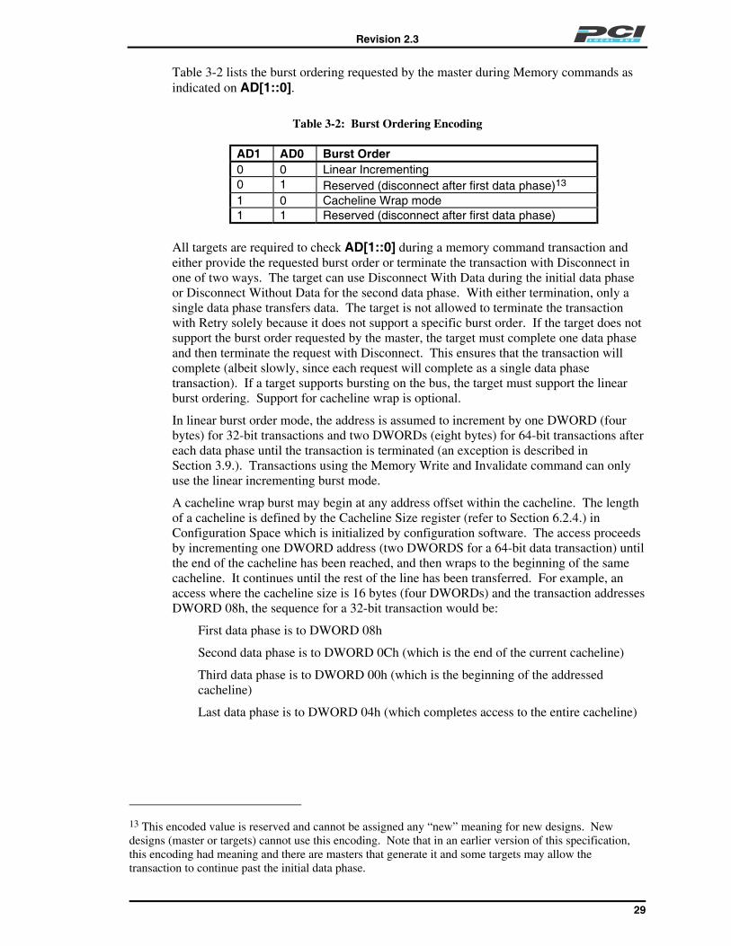
Revision 2.3
29
Table 3-2 lists the burst ordering requested by the master during Memory commands asindicated on AD[1::0].
Table 3-2: Burst Ordering Encoding
AD1 AD0 Burst Order 0 0 Linear Incrementing 0 1 Reserved (disconnect after first data phase)13
1 0 Cacheline Wrap mode 1 1 Reserved (disconnect after first data phase)
All targets are required to check AD[1::0] during a memory command transaction andeither provide the requested burst order or terminate the transaction with Disconnect inone of two ways. The target can use Disconnect With Data during the initial data phaseor Disconnect Without Data for the second data phase. With either termination, only asingle data phase transfers data. The target is not allowed to terminate the transactionwith Retry solely because it does not support a specific burst order. If the target does notsupport the burst order requested by the master, the target must complete one data phaseand then terminate the request with Disconnect. This ensures that the transaction willcomplete (albeit slowly, since each request will complete as a single data phasetransaction). If a target supports bursting on the bus, the target must support the linearburst ordering. Support for cacheline wrap is optional.
In linear burst order mode, the address is assumed to increment by one DWORD (fourbytes) for 32-bit transactions and two DWORDs (eight bytes) for 64-bit transactions aftereach data phase until the transaction is terminated (an exception is described inSection 3.9.). Transactions using the Memory Write and Invalidate command can onlyuse the linear incrementing burst mode.
A cacheline wrap burst may begin at any address offset within the cacheline. The lengthof a cacheline is defined by the Cacheline Size register (refer to Section 6.2.4.) inConfiguration Space which is initialized by configuration software. The access proceedsby incrementing one DWORD address (two DWORDS for a 64-bit data transaction) untilthe end of the cacheline has been reached, and then wraps to the beginning of the samecacheline. It continues until the rest of the line has been transferred. For example, anaccess where the cacheline size is 16 bytes (four DWORDs) and the transaction addressesDWORD 08h, the sequence for a 32-bit transaction would be:
First data phase is to DWORD 08h
Second data phase is to DWORD 0Ch (which is the end of the current cacheline)
Third data phase is to DWORD 00h (which is the beginning of the addressedcacheline)
Last data phase is to DWORD 04h (which completes access to the entire cacheline)
13 This encoded value is reserved and cannot be assigned any “new” meaning for new designs. Newdesigns (master or targets) cannot use this encoding. Note that in an earlier version of this specification,this encoding had meaning and there are masters that generate it and some targets may allow thetransaction to continue past the initial data phase.

Revision 2.3
30
If the burst continues once a complete cacheline has been accessed, the burst continues atthe same DWORD offset of the next cacheline. Continuing the burst of the previousexample would be:
Fifth data phase is to DWORD 18h
Sixth data phase is to DWORD 1Ch (which is the end of the second cacheline)
Seventh data phase is to DWORD 10h (which is the beginning of the secondcacheline)
Last data phase is to DWORD 14h (which completes access to the second cacheline)
If a target does not implement the Cacheline Size register, the target must signalDisconnect with or after the completion of the first data phase if Cacheline Wrap or areserved mode is used.
If a master starts with one burst ordering, it cannot change the burst ordering until thecurrent transaction ends, since the burst ordering information is provided on AD[1::0]during the address phase.
A device may restrict what access granularity it supports in Memory Space. Forexample, a device may restrict its driver to only access the device using byte, word, orDWORD operations and is free to terminate all other accesses with Target-Abort.
3.2.2.3. Configuration Space Decoding
Every device, other than host bus bridges, must implement Configuration Address Space.Host bus bridges may optionally implement Configuration Address Space. In theConfiguration Address Space, each function is assigned a unique 256-byte space that isaccessed differently than I/O or Memory Address Spaces. Configuration registers aredescribed in Chapter 6. The following sections describe:
• Configuration commands (Type 0 and Type 1)
• Software generation of configuration commands
• Software generation of Special Cycles
• Selection of a device’s Configuration Space
• System generation of IDSEL
3.2.2.3.1. Configuration Commands (Type 0 and Type 1)
Because of electrical loading issues, the number of devices that can be supported on agiven bus segment is limited. To allow systems to be built beyond a single bus segment,PCI-to-PCI bridges are defined. A PCI-to-PCI bridge requires a mechanism to know howand when to forward configuration accesses to devices that reside behind the bridge.
To support hierarchical PCI buses, two types of configuration transactions are used.They have the formats illustrated in Figure 3-1, which shows the interpretation of ADlines during the address phase of a configuration transaction.

Revision 2.3
31
031 10
Reserved
15 1278
DeviceNumber
16
BusNumber
Register Number
Function Number
2324
031
Reserved
1278
Register Number
Function Number 0
11
0
11 10
Type 0
Type 1
0 1
Figure 3-1: Address Phase Formats of Configuration Transactions
Type 1 and Type 0 configuration transactions are differentiated by the values onAD[1::0]. A Type 0 configuration transaction (when AD[1::0] = "00") is used to selecta device on the bus where the transaction is being run. A Type 1 configurationtransaction (when AD[1::0] = "01") is used to pass a configuration request to another bussegment.
The Register Number and Function Number fields have the same meaning for bothconfiguration types, and Device Number and Bus Number are used only in Type 1transactions. Targets must ignore reserved fields.
RegisterNumber
is an encoded value used to select a DWORD in theConfiguration Space of the intended target.
FunctionNumber
is an encoded value used to select one of eight possiblefunctions on a multifunction device.
DeviceNumber
is an encoded value used to select one of 32 devices on agiven bus. (Refer to Section 3.2.2.3.5. for limitations onthe number of devices supported.)
BusNumber
is an encoded value used to select 1 of 256 buses in asystem.
Bridges (both host and PCI-to-PCI) that need to generate a Type 0 configurationtransaction use the Device Number to select which IDSEL to assert. The FunctionNumber is provided on AD[10::08]. The Register Number is provided on AD[7::2].AD[1::0] must be "00" for a Type 0 configuration transaction.
A Type 0 configuration transaction is not propagated beyond the local PCI bus and mustbe claimed by a local device or terminated with Master-Abort.
If the target of a configuration transaction resides on another bus (not the local bus), aType 1 configuration transaction must be used. All targets except PCI-to-PCI bridgesignore Type 1 configuration transactions. PCI-to-PCI bridges decode the Bus Numberfield to determine if the destination bus of the configuration transaction resides behindthe bridge. If the Bus Number is not for a bus behind the bridge, the transaction isignored. The bridge claims the transaction if the transaction is to a bus behind the bridge.If the Bus Number is not to the secondary bus of the bridge, the transaction is simplypassed through unchanged. If the Bus Number matches the secondary bus number, thebridge converts the transaction into a Type 0 configuration transaction. The bridgechanges AD[1::0] to "00" and passes AD[10::02] through unchanged. The DeviceNumber is decoded to select one of 32 devices on the local bus. The bridge asserts the

Revision 2.3
32
correct IDSEL and initiates a Type 0 configuration transaction. Note: PCI-to-PCIbridges can also forward configuration transactions upstream (refer to the PCI-to-PCIBridge Architecture Specification for more information).
A standard expansion bus bridge must not forward a configuration transaction to anexpansion bus.
3.2.2.3.2. Software Generation of Configuration Transactions
Systems must provide a mechanism that allows software to generate PCI configurationtransactions. This mechanism is typically located in the host bridge. For PC-ATcompatible systems, the mechanism14 for generating configuration transactions is definedand specified in this section. A device driver should use the API provided by theoperating system to access the Configuration Space of its device and not directly by wayof the hardware mechanism. For other system architectures, the method of generatingconfiguration transactions is not defined in this specification.
Two DWORD I/O locations are used to generate configuration transactions for PC-ATcompatible systems. The first DWORD location (CF8h) references a read/write registerthat is named CONFIG_ADDRESS. The second DWORD address (CFCh) references aread/write register named CONFIG_DATA. The CONFIG_ADDRESS register is 32 bitswith the format shown in Figure 3-2. Bit 31 is an enable flag for determining whenaccesses to CONFIG_DATA are to be translated to configuration transactions on the PCIbus. Bits 30 to 24 are reserved, read-only, and must return 0's when read. Bits 23through 16 choose a specific PCI bus in the system. Bits 15 through 11 choose a specificdevice on the bus. Bits 10 through 8 choose a specific function in a device (if the devicesupports multiple functions). Bits 7 through 2 choose a DWORD in the device'sConfiguration Space. Bits 1 and 0 are read-only and must return 0's when read.
Enable bit ('1' = enabled, '0' = disabled)
031 10
Reserved
15 1278
DeviceNumber
16
BusNumber
RegisterNumber
FunctionNumber
2324 11
0 0
30
Figure 3-2: Layout of CONFIG_ADDRESS Register
Anytime a host bridge sees a full DWORD I/O write from the host toCONFIG_ADDRESS, the bridge must latch the data into its CONFIG_ADDRESSregister. On full DWORD I/O reads to CONFIG_ADDRESS, the bridge must return thedata in CONFIG_ADDRESS. Any other types of accesses to this address (non-DWORD) have no effect on CONFIG_ADDRESS and are executed as normal I/Otransactions on the PCI bus. Therefore, the only I/O Space consumed by this register is aDWORD at the given address. I/O devices that share the same address but use BYTE orWORD registers are not affected because their transactions will pass through the hostbridge unchanged.
When a host bridge sees an I/O access that falls inside the DWORD beginning atCONFIG_DATA address, it checks the Enable bit and the Bus Number in theCONFIG_ADDRESS register. If the Enable bit is set and the Bus Number matches the
14 In versions 2.0 and 2.1 of this specification, two mechanisms were defined. However, only onemechanism (Configuration Mechanism #1) was allowed for new designs and the other (ConfigurationMechanism #2) was included for reference.

Revision 2.3
33
bridge's Bus Number or any Bus Number behind the bridge, a configuration cycletranslation must be done.
There are two types of translation that take place. The first, Type 0, is a translation wherethe device being addressed is on the PCI bus connected to the host bridge. The second,Type 1, occurs when the device is on another bus somewhere behind this bridge.
For Type 0 translations (see Figure 3-3), the host bridge does a decode of the DeviceNumber field to assert the appropriate IDSEL line15 and performs a configurationtransaction on the PCI bus where AD[1::0] = "00". Bits 10 - 8 of CONFIG_ADDRESSare copied to AD[10::8] on the PCI bus as an encoded value which is used bycomponents that contain multiple functions. AD[7::2] are also copied from theCONFIG_ADDRESS register. Figure 3-3 shows the translation from theCONFIG_ADDRESS register to AD lines on the PCI bus.
0 0RegisterNumber
DeviceNumber
BusNumberReserved
1278111516232431 30 010
01011
Only One ‘1’ 0 0
31
CONFIG_ADDRESS
PCI AD BUS
FunctionNumber
Enable bit‘1’ = enabled‘0’ = disabled
Figure 3-3: Host Bridge Translation for Type 0 Configuration Transactions Address Phase
For Type 1 translations, the host bridge directly copies the contents of theCONFIG_ADDRESS register (excluding bits 31 and 0) onto the PCI AD lines during theaddress phase of a configuration transaction making sure that AD[1::0] is "01".
In both Type 0 and Type 1 translations, byte enables for the data transfers must bedirectly copied from the processor bus.
15 If the Device Number field selects an IDSEL line that the bridge does not implement, the bridge mustcomplete the processor access normally, dropping the data on writes and returning all ones on reads. Thebridge may optionally implement this requirement by performing a Type 0 configuration access with noIDSEL asserted. This will terminate with Master-Abort which drops write data and returns all ones onreads.
Revision 2.3
34
Implementation Note: Bus Number Registers and Peer Host Bridges For host bridges that do not support peer host buses, translating configuration accessesinto configuration transactions is simple. If the Bus Number in the CONFIG_ADDRESSregister is zero, a Type 0 configuration translation is used. If the Bus Number in theCONFIG_ADDRESS register is non-zero, a Type 1 configuration translation is used.
For host bridges that support peer host buses, one peer bridge typically is designated toalways acknowledge accesses to the CONFIG_ADDRESS register. Other peer bridgeswould snoop the data written to this register. Accesses to the CONFIG_DATA registerare typically handshaken by the bridge doing the configuration translation.
Host bridges that support peer host buses require two Configuration Space registerswhose contents are used to determine when the bridge does configuration transactiontranslation. One register (Bus Number) specifies the bus number of the PCI bus directlybehind the bridge, and the other register (Subordinate Bus Number) specifies the numberof the last hierarchical bus behind the bridge. (A PCI-to-PCI bridge requires an additionalregister, which is its Primary Bus Number.) System configuration software is responsiblefor initializing these registers to appropriate values. The host bridge determines theconfiguration translation type (1 or 0) based on the value of the bus number in theCONFIG_ADDRESS register. If the Bus Number in the CONFIG_ADDRESS registermatches the Bus Number register, a Type 0 configuration transaction is used. If the BusNumber in CONFIG_ADDRESS is greater than the Bus Number register and less than orequal to the Subordinate Bus Number register, a Type 1 configuration transaction is used.If the Bus Number in CONFIG_ADDRESS is less than the Bus Number register orgreater than the Subordinate Bus Number register, the configuration transaction isaddressing a bus that is not implemented or is behind some other host bridge and isignored.
3.2.2.3.3. Software Generation of Special Cycles
This section defines how a host bridge in a PC-AT compatible systems may optionallyimplement the configuration mechanism for accessing Configuration Space to allowsoftware to generate a transaction that uses a Special Cycle command. Host bridges arenot required to provide a mechanism for allowing software to generate a transaction usinga Special Cycle command.
When the CONFIG_ADDRESS register is written with a value such that the Bus Numbermatches the bridge's bus number, the Device Number is all 1's, the Function Number isall 1's, and the Register Number has a value of zero, then the bridge is primed to generatea transaction using a Special Cycle command the next time the CONFIG_DATA registeris written. When the CONFIG_DATA register is written, the bridge generates atransaction that uses a Special Cycle command encoding (rather than Configuration Writecommand) on the C/BE[3::0]# pins during the address phase and drives the data fromthe I/O write onto AD[31::00] during the first data phase. After CONFIG_ADDRESShas been set up this way, reads to CONFIG_DATA have undefined results. In onepossible implementation, the bridge can treat it as a normal configuration operation (i.e.,generate a Type 0 configuration transaction on the PCI bus). This will terminate with aMaster-Abort and the processor will have all 1's returned.
If the Bus Number field of CONFIG_ADDRESS does not match the bridge's busnumber, then the bridge passes the write to CONFIG_DATA on through to PCI as a Type1 configuration transaction just like any other time the bus numbers do not match.

Revision 2.3
35
3.2.2.3.4. Selection of a Device’s Configuration Space
Accesses in the Configuration Address Space require device selection decoding to bedone externally and to be signaled to the device via initialization device select, or IDSEL,which functions as a classical “chip select” signal. Each device has its own IDSEL input(except for host bus bridges, which are permitted to implement their initialization deviceselection internally).
Devices that respond to Type 0 configuration cycles are separated into two types and aredifferentiated by an encoding in the Configuration Space header. The first type (single-function device) is defined for backward compatibility and only uses its IDSEL pin andAD[1::0] to determine whether or not to respond.
A single function device asserts DEVSEL# to claim a configuration transaction when:• a configuration command is decoded;• the device’s IDSEL is asserted; and• AD[1::0] is "00" (Type 0 Configuration Command) during the Address Phase.
Otherwise, the device ignores the current transaction. A single-function device mayoptionally respond to all function numbers as the same function or may decode theFunction Number field, AD[10::08], and respond only to function 0 and not respond(Master-Abort termination) to the other function numbers.
The second type of device (multi-function device) decodes the Function Number fieldAD[10::08] to select one of eight possible functions on the device when determiningwhether or not to respond. Multi-function devices are required to do a full decode onAD[10::08] and only respond to the configuration cycle if they have implemented theConfiguration Space registers for the selected function. They must not respond (Master-Abort termination) to unimplemented function numbers. They are also required toalways implement function 0 in the device. Implementing other functions is optional andmay be assigned in any order (i.e., a two-function device must respond to function 0 butcan choose any of the other possible function numbers (1-7) for the second function).
If a device implements multiple independent functions, it asserts DEVSEL# to claim aconfiguration transaction when:• a configuration command is decoded;• the target’s IDSEL is asserted;• AD[1::0] is "00"; and• AD[10::08] match a function that is implemented.
Otherwise, the transaction is ignored. For example, if functions 0 and 4 are implemented(functions 1 through 3 and 5 through 7 are not), the device would assert DEVSEL# for aconfiguration transaction in which IDSEL is asserted and AD[1::0] are 00 andAD[10::08] matches 000 or 100. AD[31::11] are ignored by a multi-function deviceduring an access of its configuration registers.
The order in which configuration software probes devices residing on a bus segment isnot specified. Typically, configuration software either starts with Device Number 0 andworks up or starts at Device Number 31 and works down. If a single function device isdetected (i.e., bit 7 in the Header Type register of function 0 is 0), no more functions forthat Device Number will be checked. If a multi-function device is detected (i.e., bit 7 inthe Header Type register of function 0 is 1), then all remaining Function Numbers will bechecked.
Once a function has been selected, it uses AD[7::2] to address a DWORD and the byteenables to determine which bytes within the addressed DWORD are being accessed. Afunction must not restrict the size of the access it supports in Configuration Space. The

Revision 2.3
36
configuration commands, like other commands, allow data to be accessed using anycombination of bytes (including a byte, word, DWORD, or non-contiguous bytes) andmultiple data phases in a burst. The target is required to handle any combination of byteenables. However, it is not required to handle a configuration transaction that consists ofmultiple data phases. If a configuration transaction consists of more than a single dataphase, the target is permitted to terminate the request with Disconnect. This is notsufficient cause for the target to terminate the transaction with Target-Abort, since this isnot an error condition.
If a configuration transaction has multiple data phases (burst), linear burst ordering is theonly addressing mode allowed, since AD[1::0] convey configuration transaction type andnot a burst addressing mode like Memory accesses. The implied address of eachsubsequent data phase is one DWORD larger than the previous data phase. For example,a transaction starts with AD[7::2] equal to 0000 00xxb, the sequence of a burst would be:0000 01xxb, 0000 10xxb, 0000 11xxb, 0001 00xxb (where xx indicate whether thetransaction is a Type 00 or Type 01 configuration transaction). The rest of thetransaction is the same as other commands including all termination semantics.Note: The PCI-to-PCI Bridge Architecture Specification restricts Type 1 configurationtransactions that are converted into a transaction that uses a Special Cycle command to asingle data phase (no Special Cycle bursts).
If no agent responds to a configuration transaction, the request is terminated via Master-Abort (refer to Section 3.3.3.1.).
3.2.2.3.5. System Generation of IDSEL
Exactly how the IDSEL pin is driven is left to the discretion of the host/memory bridgeor system designer. This signal has been designed to allow its connection to one of theupper 21 address lines, which are not otherwise used in a configuration access. However,there is no specified way of determining IDSEL from the upper 21 address bits.Therefore, the IDSEL pin must be supported by all targets. Devices must not make aninternal connection between an AD line and an internal IDSEL signal in order to save apin. The only exception is the host bridge, since it defines how IDSELs are mapped.IDSEL generation behind a PCI-to-PCI bridge is specified in the PCI-to-PCI BridgeArchitecture Specification.
The binding between a device number in the CONFIG_ADDRESS register of PC-ATcompatible system and the generation of an IDSEL is not specified. Therefore, BIOSmust scan all 32 device numbers to ensure all components are located. Note: Thehardware that converts the device number to an IDSEL is required to ensure that only asingle unique IDSEL line is asserted for each device number. Configuration transactionsthat are not claimed by a device are terminated with Master-Abort. The master thatinitiated this transaction sets the received Master-Abort bit in the Status register.

Revision 2.3
37
Implementation Note: System Generation of IDSEL How a system generates IDSEL is system specific; however, if no other mapping isrequired, the following example may be used. The IDSEL signal associated with DeviceNumber 0 is connected to AD[16], IDSEL of Device Number 1 is connected to AD[17],and so forth until IDSEL of Device Number 15 is connected to AD[31]. For DeviceNumbers 17-31, the host bridge should execute the transaction but not assert any of theAD[31::16] lines but allow the access to be terminated with Master-Abort.
Twenty-one different devices can be uniquely selected for configuration accesses byconnecting a different address line to each device and asserting one of the AD[31::11]lines at a time. The issue with connecting one of the upper 21 AD lines to IDSEL is anadditional load on the AD line. This can be mitigated by resistively coupling IDSEL tothe appropriate AD line. This does, however, create a very slow slew rate on IDSEL,causing it to be in an invalid logic state most of the time, as shown in Figure 3-4 with the"XXXX" marks. However, since it is only used on the address phase of a Type 0configuration transaction, the address bus can be pre-driven a few clocks beforeFRAME#16, thus guaranteeing IDSEL to be stable when it needs to be sampled. Pre-driving the address bus is equivalent to IDSEL stepping as discussed in Section 3.6.3.Note that if resistive coupling is used, the bridge that generates the configurationtransaction is required to use IDSEL stepping or ensure that the clock period issufficiently long to allow IDSEL to become stable before initiating the configurationtransaction. For all other cycles, IDSEL is undefined and may be at a non-deterministiclevel during the address phase.
16 The number of clocks the address bus should be pre-driven is determined from the RC time constant onIDSEL.

Revision 2.3
38
FRAME#
CLK
TRDY#
IRDY#
AD
C/BE#
ADDRESS
BE#'s
DATA
CFG-RD
IDSEL
1 2 3 4 5 6
DEVSEL#
Figure 3-4: Configuration Read
3.2.3. Byte Lane and Byte Enable Usage
The bus protocol does not support automatic bus sizing on requests of a DWORD or less.(Automatic bus sizing allows a device to request the master of the current transaction tobreak the access into smaller pieces for the target to complete. For example, an 8-bitdevice that is accessed with a 16-bit request could transfer the lower 8 bits and require themaster to move the upper 8 bits (of the 16-bit access) down to the lower byte lane tocomplete the request.) Since all PCI devices connect to the lower 32 bits for addressdecode, the device itself is required to provide this byte steering when required, or thedriver is required to place the data on the correct byte. In general, software is aware ofthe characteristics of the target device and only issues appropriate length accesses.
The bus protocol requires automatic bus sizing if a master requests a 64-bit data transferto a 32-bit target. In this case, the target does not indicate that it can do a 64-bit datatransfer, and the master is required to complete the current transaction using 32-bit datatransfers. For more details about 64-bit data transactions, refer to Section 3.8.
The byte enables alone are used to determine which byte lanes carry meaningful data.The byte enables are free to change between data phases but must be valid on the clockthat starts each data phase and must stay valid for the entire data phase. In Figure 3-5,data phases begin on clocks 3, 5, and 7. (Changing byte enables during a read bursttransaction is generally not useful, but is permitted.) The master is free to change thebyte enables on each new data phase (although the read diagram does not show this). Ifthe master changes byte enables on a read transaction, it does so with the same timing aswould be used in a write transaction. If byte enables are important for the target on aread transaction, the target must wait for the byte enables to be valid on each data phasebefore completing the transfer; otherwise, it must return all bytes. Note: Byte enablesare valid during the entire data phase independent of the state of IRDY#.

Revision 2.3
39
If a target supports prefetching (bit 3 is set in the Memory Base Address register -- referto Section 6.2.5.1.), it must also return all data17 regardless of which byte enables areasserted. A target can only operate in this mode when there are no side effects (datadestroyed or status changes because of the access).
PCI allows any contiguous or non-contiguous combination of byte enables. If no byteenables are asserted, the target of the access must complete the data phase by assertingTRDY# and providing parity if the transaction is a read request. The target of an accesswhere no byte enables are asserted must complete the current data phase without anystate change. On a read transaction, this means that data and status are not changed. Ifcompleting the access has no affect on the data or status, the target may complete theaccess by either providing data or not. The generation and checking of parity is the sameregardless of the state of the byte enables for both 32-bit and 64-bit data transfers. For adiscussion on parity generation and checking, refer to Section 3.7.1. (32-bit transactions)and Section 3.8. (64-bit transactions).
However, some targets may not be able to properly interpret non-contiguous patterns(e.g., expansion bus bridges that interface to 8- and 16-bit devices). Expansion busbridges may optionally report patterns that are illegal on the expansion bus as anasynchronous error (SERR#) or break the transaction into smaller transactions that arelegal for the intended agent. The target of an I/O transaction is required to signal Target-Abort if it is unable to complete the entire access defined by the byte enables.
3.2.4. Bus Driving and Turnaround
A turnaround cycle is required on all signals that are driven by more than one agent. Theturnaround cycle is required to avoid contention when one agent stops driving a signaland another agent begins driving the signal. This is indicated on the timing diagrams astwo arrows pointing at each others' tail. This turnaround cycle occurs at different timesfor different signals. For instance, IRDY#, TRDY#, DEVSEL#, STOP#, and ACK64#use the address phase as their turnaround cycle. FRAME#, REQ64#, C/BE[3::0]#,C/BE[7::4]#, AD[31::00], and AD[63::32] use the Idle state between transactions astheir turnaround cycle. The turnaround cycle for LOCK# occurs one clock after thecurrent owner releases it. PERR# has a turnaround cycle on the fourth clock after thelast data phase, which is three clocks after the turnaround-cycle for the AD lines. An Idlestate is when both FRAME# and IRDY# are deasserted (e.g., clock 9 in Figure 3-5).
All AD lines (including AD[63::32] when the master supports a 64-bit data path) mustbe driven to stable values during 64-bit transfers every address and data phase. Evenbyte lanes not involved in the current data transfer must physically drive stable (albeitmeaningless) data onto the bus. The motivation is for parity calculations and to keepinput buffers on byte lanes not involved in the transfer from switching at the thresholdlevel and, more generally, to facilitate fast metastability-free latching. In power-sensitiveapplications, it is recommended that in the interest of minimizing bus switching powerconsumption, byte lanes not being used in the current bus phase should be driven with thesame data as contained in the previous bus phase. In applications that are not powersensitive, the agent driving the AD lines may drive whatever it desires on unused bytelanes. Parity must be calculated on all bytes regardless of the byte enables.
3.2.5. Transaction Ordering and Posting
17 For a 32-bit data transfer, this means 4 bytes per data phase; for a 64-bit data transfer, this means 8 bytesper data phase.

Revision 2.3
40
Transaction ordering rules on PCI accomplish three things. First, they satisfy the write-results ordering requirements of the Producer-Consumer Model. This means that theresults of writes from one master (the Producer) anywhere in the system are observableby another master (the Consumer) anywhere in the system only in their original order.(Different masters (Producers) in different places in the system have no fundamental needfor their writes to happen in a particular order with respect to each other, since each willhave a different Consumer. In this case, the rules allow for some writes to berearranged.) Refer to Appendix E for a complete discussion of the Producer-ConsumerModel. Second, they allow for some transactions to be posted to improve performance.And third, they prevent bus deadlock conditions, when posting buffers have to be flushedto meet the first requirement.
The order relationship of a given transaction with respect to other transactions isdetermined when it completes; i.e., when data is transferred. Transactions whichterminate with Retry have not completed since no data was transferred and, therefore,have no ordering requirements relative to each other. Transactions that terminate withMaster-Abort or Target-Abort are considered completed with or without data beingtransferred and will not be repeated by the master. The system may accept requests inany order, completing one while continuing to Retry another. If a master requires onetransaction to be completed before another, the master must not attempt the secondtransaction until the first one is complete. If a master has only one outstanding request ata time, then that master’s transactions will complete throughout the system in the sameorder the master executed them. Refer to Section 3.3.3.3.5. for further discussion ofrequest ordering.
Transactions can be divided into two general groups based on how they are handled by anintermediate agent, such as a bridge. The two groups are posted and non-postedtransactions. Posted transactions complete at the originating device before they reachtheir ultimate destination. The master will often proceed with other work, sometimesincluding other bus transactions, before the posted transaction reaches it ultimatedestination. In essence, the intermediate agent of the access (e.g., a bridge) accepts thedata on behalf of the actual target and assumes responsibility for ensuring that the accesscompletes at the final destination. Memory writes (Memory Write and Memory Writeand Invalidate commands) are allowed to be posted on the PCI bus.
Non-posted transactions reach their ultimate destination before completing at theoriginating device. The master cannot proceed with any other work until the transactionhas completed at the ultimate destination (if a dependency exists). Memory readtransactions (Memory Read, Memory Read Line, and Memory Read Multiple), I/Otransactions (I/O Read and I/O Write), and configuration transactions (ConfigurationRead and Configuration Write) are non-posted (except as noted below for host bridges).
There are two categories of devices with different requirements for transaction orderingand posting. Each category will be presented separately.

Revision 2.3
41
3.2.5.1. Transaction Ordering and Posting for Simple Devices
A simple device is any device that while acting as a bus master does not require its writedata to be posted at the bus interface logic. Generally devices that do not connect to localCPUs are implemented as simple devices.
The target and master state machines in the PCI interface of a simple device arecompletely independent. A device cannot make the completion of any transaction (eitherposted or non-posted) as a target contingent upon the prior completion of any othertransaction as a master. Simple devices are allowed to terminate a transaction with Retryonly to execute the transaction as a Delayed Transaction or for temporary conditionswhich are guaranteed to be resolved with time; e.g., during a video screen refresh orwhile a transaction buffer is filled with transactions moving in the same direction. (Referto Section 3.5.3. for a limit on the length of time a memory write transaction can beterminated with Retry.)
Implementation Note: Deadlock When Target and Master NotIndependent The following is an example of a deadlock that could occur if devices do not make theirtarget and master interfaces independent.
Suppose two devices, Device A and Device B, are talking directly to each other. Bothdevices attempt I/O writes to each other simultaneously. Suppose Device A is grantedthe bus first and executes its I/O write addressing Device B. Device B decodes itsaddress and asserts DEVSEL#. Further, suppose that Device B violates the requirementfor the target state machine to be independent of the master state machine and alwaysterminates transactions as a target with Retry until its master state machine completes itsoutstanding requests. Since Device B also has an I/O transaction it must execute as amaster, it terminates Device A’s transaction with Retry.
Device B is then granted the bus, and Device B executes its I/O write addressing DeviceA. If Device A responds the same way Device B did, the system will deadlock.

Revision 2.3
42
Implementation Note: Deadlock When Posted Write Data is NotAccepted Deadlocks can also occur when a device does not accept a memory write transaction froma bridge. As described below, a bridge is required in certain cases to flush its postingbuffer as a master before it completes a transaction as a target. Suppose a PCI-to-PCIbridge contains posted memory write data addressed to a downstream device. But beforethe bridge can acquire the downstream bus to do the write transaction, a downstreamdevice initiates a read from host memory. Since requirement 3 in the bridge rulespresented below states that posting buffers must be flushed before a read transaction canbe completed, the bridge must Retry the agent’s read and attempt a write transaction. Ifthe downstream device were to make the acceptance of the write data contingent upon theprior completion of the retried read transaction (that is, if it could not accept the postedwrite until it first completed the read transaction), the bus would be deadlocked.
Since certain PCI-to-PCI bridge devices designed to previous versions of thisspecification require their posting buffer to be flushed before starting any non-postedtransaction, the same deadlock could occur if the downstream device makes theacceptance of a posted write contingent on the prior completion of any non-postedtransaction.
The required independence of target and master state machines in a simple device impliesthat a simple device cannot internally post any outbound transactions. For example, ifduring the course of performing its intended function a device must execute a memorywrite as a master on the PCI bus, the device cannot post that memory write in the masterinterface of the device. More specifically, the device cannot proceed to other internaloperations such as updating status registers that would be observable by another master inthe system. The simple device must wait until the memory write transaction completeson the PCI bus (TRDY# asserted; Master-Abort or Target-Abort) before proceedinginternally.
Simple devices are strongly encouraged to post inbound memory write transactions tospeed the transaction on the PCI bus. How such a device deals with ordering of inboundposted write data is strictly implementation dependent and beyond the scope of thisspecification.
Simple devices do not support exclusive accesses and do not use the LOCK# signal.Refer to Appendix F for a discussion of the use of LOCK# in bridge devices.
3.2.5.2. Transaction Ordering and Posting for Bridges
A bridge device is any device that implements internal posting of outbound memorywrite transactions, i.e., write transactions that must be executed by the device as a masteron the PCI bus. Bridges normally join two buses such as two PCI buses, a host bus and aPCI bus, or a PCI bus and a bus for a local CPU; i.e., a peripheral CPU.

Revision 2.3
43
Bridges are permitted to post memory write transactions moving in either directionthrough the bridge. The following ordering rules guarantee that the results of onemaster’s write transactions are observable by other masters in the proper order, eventhough the write transaction may be posted in a bridge. They also guarantee that the busdoes not deadlock when a bridge tries to empty its posting buffers.
• Posted memory writes moving in the same direction through a bridge will completeon the destination bus in the same order they complete on the originating bus. Evenif a single burst on the originating bus is terminated with Disconnect on thedestination bus so that it is broken into multiple transactions, those transactions mustnot allow the data phases to complete on the destination bus in any order other thantheir order on the originating bus.
• Write transactions flowing in one direction through a bridge have no orderingrequirements with respect to writes flowing in the other direction through the bridge.
• Posted memory write buffers in both directions must be flushed before completing aread transaction in either direction. Posted memory writes originating on the sameside of the bridge as a read transaction, and completing before the read commandcompletes on the originating bus, must complete on the destination bus in the sameorder. Posted memory writes originating on the opposite side of the bridge from aread transaction and completing on the read-destination bus before the read commandcompletes on the read-destination bus must complete on the read-origin bus in thesame order. In other words, a read transaction must push ahead of it through thebridge any posted writes originating on the same side of the bridge and posted beforethe read. In addition, before the read transaction can complete on its originating bus,it must pull out of the bridge any posted writes that originated on the opposite sideand were posted before the read command completes on the read-destination bus.
• A bridge can never make the acceptance (posting) of a memory write transaction as atarget contingent on the prior completion of a non-locked transaction as a master onthe same bus. A bridge can make the acceptance of a memory write transaction as atarget contingent on the prior completion of a locked transaction as a master only ifthe bridge has already established a locked operation with its intended target;otherwise, a deadlock may occur. (Refer to Appendix F for a discussion of the use ofLOCK# in bridge devices.) In all other cases, bridges are allowed to refuse to accepta memory write only for temporary conditions which are guaranteed to be resolvedwith time, e.g., during a video screen refresh or while the memory buffer is filled byprevious memory write transactions moving in the same direction.
Host bus bridges are permitted to post I/O write transactions that originate on the host busand complete on a PCI bus segment when they follow the ordering rules described in thisspecification and do not cause a deadlock. This means that when a host bus bridge postsan I/O write transaction that originated on the host bus, it must provide a deadlock freeenvironment when the transaction completes on PCI. The transaction will complete onthe destination PCI bus before completing on the originating PCI bus.
Since memory write transactions may be posted in bridges anywhere in the system, andI/O writes may be posted in the host bus bridge, a master cannot automatically tell whenits write transaction completes at the final destination. For a device driver to guaranteethat a write has completed at the actual target (and not at an intermediate bridge), it mustcomplete a read to the same device that the write targeted. The read (memory or I/O)forces all bridges between the originating master and the actual target to flush all posteddata before allowing the read to complete. For additional details on device drivers, referto Section 6.5. Refer to Section 3.10., item 6, for other cases where a read is necessary.

Revision 2.3
44
Interrupt requests (that use INTx#) do not appear as transactions on the PCI bus (they aresideband signals) and, therefore, have no ordering relationship to any bus transactions.Furthermore, the system is not required to use the Interrupt Acknowledge bus transactionto service interrupts. So interrupts are not synchronizing events and device driverscannot depend on them to flush posting buffers. However, when MSI are used, they havethe same ordering rules as a memory write transaction (refer to Section 6.8. for moreinformation).
3.2.6. Combining, Merging, and Collapsing
Under certain conditions, bridges that receive (write) data may attempt to convert atransaction (with a single or multiple data phases) into a larger transaction to optimize thedata transfer on PCI. The terms used when describing the action are: combining,merging, and collapsing. Each term will be defined and the usage for bridges (host, PCI-to-PCI, or standard expansion bus) will be discussed.
Combining -- occurs when sequential memory write transactions (single data phase orburst and independent of active byte enables) are combined into a single PCI bustransaction (using linear burst ordering).
The combining of data is not required but is recommended whenever posting of writedata is being done. Combining is permitted only when the implied ordering is notchanged. Implied ordering means that the target sees the data in the same order as theoriginal master generated it. For example, a write sequence of DWORD 1, 2, and 4 canbe converted into a burst sequence. However, a write of DWORD 4, 3, and 1 cannot becombined into a burst but must appear on PCI as three separate transactions in the sameorder as they occurred originally. Bursts may include data phases that have no byteenables asserted. For example, the sequence DWORD 1, 2, and 4 could be combinedinto a burst in which data phase 1 contains the data and byte enables provided withDWORD 1. The second data phase of the burst uses data and byte enables provided withDWORD 2, while data phase 3 asserts no byte enables and provides no meaningful data.The burst completes with data phase 4 using data and byte enables provided withDWORD 4.
If the target is unable to handle multiple data phases for a single transaction, it terminatesthe burst transaction with Disconnect with or after each data phase. The target sees thedata in the same order the originating master generated it, whether the transaction wasoriginally generated as a burst or as a series of single data phase accesses which werecombined into a burst.
Byte Merging -- occurs when a sequence of individual memory writes (bytes or words)are merged into a single DWORD.
The merging of bytes within the same DWORD for 32-bit transfers or QUADWORD(eight bytes) for 64-bit transfers is not required but is recommended when posting ofwrite data is done. Byte merging is permitted only when the bytes within a data phase arein a prefetchable address range. While similar to combining in concept, merging can bedone in any order (within the same data phase) as long as each byte is only written once.For example, in a sequence where bytes 3, 1, 0, and 2 are written to the same DWORDaddress, the bridge could merge them into a single data phase memory write on PCI withByte Enable 0, 1, 2, and 3 all asserted instead of four individual write transactions.However, if the sequence written to the same DWORD address were byte 1, and byte 1again (with the same or different data), byte 2, and byte 3, the bridge cannot merge thefirst two writes into a single data phase because the same byte location must be writtentwice. However, the last three transactions could be merged into a single data phase with

Revision 2.3
45
Byte Enable 0 being deasserted and Byte Enable 1, 2, and 3 being asserted. Merging cannever be done to a range of I/O or Memory Mapped I/O addresses (not prefetchable).
Note: Merging and combining can be done independently of each other. Bytes within aDWORD may be merged and merged DWORDs can be combined with other DWORDswhen conditions allow. A device can implement only byte merging, only combining,both byte merging and combining, or neither byte merging or combining.
Collapsing -- is when a sequence of memory writes to the same location (byte, word, orDWORD address) are collapsed into a single bus transaction.
Collapsing is not permitted by PCI bridges (host, PCI-to-PCI, or standard expansion)except as noted below. For example, a memory write transaction with Byte Enable 3asserted to DWORD address X, followed by a memory write access to the same address(X) as a byte, word, or DWORD, or any other combination of bytes allowed by PCIwhere Byte Enable 3 is asserted, cannot be merged into a single PCI transaction. Thesetwo accesses must appear on PCI as two separate and distinct transactions.
Note: The combining and merging of I/O and Configuration transactions are notallowed. The collapsing of data of any type of transaction (Configuration, Memory, orI/O) is never allowed (except where noted below).
Note: If a device cannot tolerate memory write combining, it has been designedincorrectly. If a device cannot tolerate memory write byte merging, it must mark itself asnot prefetchable. (Refer to Section 6.2.5.1. for a description of prefetchable.) A devicethat marks itself prefetchable must tolerate combining (without reordering) and bytemerging (without collapsing) of writes as described previously. A device is explicitly notrequired to tolerate reordering of DWORDs or collapsing of data. A prefetchable addressrange may have write side effects, but it may not have read side effects. A bridge (hostbus, PCI-to-PCI, or standard expansion bus) cannot reorder DWORDs in any space, evenin a prefetchable space.
Bridges may optionally allow data to be collapsed in a specific address range when adevice driver indicates that there are no adverse side-effects due to collapsing. How adevice driver indicates this to the system is beyond the scope of this specification.
Revision 2.3
46
Implementation Note: Combining, Merging, and Collapsing Bridges that post memory write data should consider implementing Combining and ByteMerging. The collapsing of multiple memory write transactions into a single PCI bustransaction is never allowed (except as noted above). The combining of sequentialDWORD memory writes into a PCI burst has significant performance benefits. Forexample, a processor is doing a large number of DWORD writes to a frame buffer. Whenthe host bus bridge combines these accesses into a single PCI transaction, the PCI bus cankeep up with a host bus that is running faster and/or wider than PCI.
The merging of bytes within a single DWORD provides a performance improvement butnot as significant as combining. However, for unaligned multi-byte data transfersmerging allows the host bridge to merge misaligned data into single DWORD memorywrite transactions. This reduces (at a minimum) the number of PCI transactions by afactor of two. When the bridge merges bytes into a DWORD and then combinesDWORDs into a burst, the number of transactions on PCI can be reduced even furtherthan just by merging. With the addition of combining sequential DWORDs, the numberof transactions on PCI can be reduced even further. Merging data (DWORDs) within asingle cacheline appears to have minimal performance gains.
3.3. Bus Transactions The timing diagrams in this section show the relationship of significant signals involvedin 32-bit transactions. When a signal is drawn as a solid line, it is actively being drivenby the current master or target. When a signal is drawn as a dashed line, no agent isactively driving it. However, it may still be assumed to contain a stable value if thedashed line is at the high rail. Tri-stated signals are indicated to have indeterminatevalues when the dashed line is between the two rails (e.g., AD or C/BE# lines). When asolid line becomes a dotted line, it indicates the signal was actively driven and now is tri-stated. When a solid line makes a low to high transition and then becomes a dotted line,it indicates the signal was actively driven high to precharge the bus and then tri-stated.The cycles before and after each transaction will be discussed in Section 3.4.

Revision 2.3
47
3.3.1. Read Transaction
Figure 3-5 illustrates a read transaction and starts with an address phase which occurswhen FRAME# is asserted for the first time and occurs on clock 2. During the addressphase, AD[31::00] contain a valid address and C/BE[3::0]# contain a valid buscommand.
FRAME#
CLK
TRDY#
IRDY#
AD
DEVSEL#
C/BE#
ADDRESS
BUS CMD
DATA-1 DATA-2 DATA-3
BE#'s
1 2 3 4 5 6 7 8 9
DA
TA
TR
AN
SF
ER
DA
TA
TR
AN
SF
ER
DA
TA
TR
AN
SF
ER
WA
IT
ADDRESSPHASE
DATAPHASE
DATAPHASE
WA
IT
DATAPHASE
WA
IT
BUS TRANSACTION
Figure 3-5: Basic Read Operation
The first clock of the first data phase is clock 3. During the data phase, C/BE# indicatewhich byte lanes are involved in the current data phase. A data phase may consist of waitcycles and a data transfer. The C/BE# output buffers must remain enabled (for both readand writes) from the first clock of the data phase through the end of the transaction. Thisensures C/BE# are not left floating for long intervals. The C/BE# lines contain validbyte enable information during the entire data phase independent of the state of IRDY#.The C/BE# lines contain the byte enable information for data phase N+1 on the clockfollowing the completion of the data phase N. This is not shown in Figure 3-5 because aburst read transaction typically has all byte enables asserted; however, it is shown inFigure 3-6. Notice on clock 5 in Figure 3-6, the master inserted a wait state bydeasserting IRDY#. However, the byte enables for data phase 3 are valid on clock 5 andremain valid until the data phase completes on clock 8.
The first data phase on a read transaction requires a turnaround-cycle (enforced by thetarget via TRDY#). In this case, the address is valid on clock 2 and then the master stopsdriving AD. The earliest the target can provide valid data is clock 4. The target mustdrive the AD lines following the turnaround cycle when DEVSEL# is asserted. Onceenabled, the output buffers must stay enabled through the end of the transaction. (Thisensures that the AD lines are not left floating for long intervals.)
One way for a data phase to complete is when data is transferred, which occurs whenboth IRDY# and TRDY# are asserted on the same rising clock edge. There are otherconditions that complete a data phase and these are discussed in Section 3.3.3.2.(TRDY# cannot be driven until DEVSEL# is asserted.) When either IRDY# or TRDY#

Revision 2.3
48
is deasserted, a wait cycle is inserted and no data is transferred. As noted in Figure 3-5,data is successfully transferred on clocks 4, 6, and 8 and wait cycles are inserted onclocks 3, 5, and 7. The first data phase completes in the minimum time for a readtransaction. The second data phase is extended on clock 5 because TRDY# is deasserted.The last data phase is extended because IRDY# was deasserted on clock 7.
The master knows at clock 7 that the next data phase is the last. However, because themaster is not ready to complete the last transfer (IRDY# is deasserted on clock 7),FRAME# stays asserted. Only when IRDY# is asserted can FRAME# be deasserted asoccurs on clock 8, indicating to the target that this is the last data phase of the transaction.
3.3.2. Write Transaction
Figure 3-6 illustrates a write transaction. The transaction starts when FRAME# isasserted for the first time which occurs on clock 2. A write transaction is similar to aread transaction except no turnaround cycle is required following the address phasebecause the master provides both address and data. Data phases work the same for bothread and write transactions.
FRAME#
CLK
TRDY#
IRDY#
AD
DEVSEL#
C/BE#
ADDRESS
BUS CMD
DATA-3
1 2 3 4 5 6 7 8 9
ADDRESSPHASE
DATAPHASE
DATAPHASE
DA
TA
TR
AN
SF
ER
DA
TA
TR
AN
SF
ER
WA
IT
WA
IT
DATA-1 DATA-2
WA
IT
DA
TA
TR
AN
SF
ER
DATAPHASE
BE#'s-1 BE#'s-3BE#'s-2
BUS TRANSACTION
Figure 3-6: Basic Write Operation
In Figure 3-6, the first and second data phases complete with zero wait cycles. However,the third data phase has three wait cycles inserted by the target. Notice both agents inserta wait cycle on clock 5. IRDY# must be asserted when FRAME# is deassertedindicating the last data phase.
The data transfer was delayed by the master on clock 5 because IRDY# was deasserted.The last data phase is signaled by the master on clock 6, but it does not complete untilclock 8.
Note: Although this allowed the master to delay data, it did not allow the byte enables tobe delayed.

Revision 2.3
49
3.3.3. Transaction Termination
Termination of a PCI transaction may be initiated by either the master or the target.While neither can actually stop the transaction unilaterally, the master remains in ultimatecontrol, bringing all transactions to an orderly and systematic conclusion regardless ofwhat caused the termination. All transactions are concluded when FRAME# and IRDY#are both deasserted, indicating an Idle state (e.g., clock 9 in Figure 3-6).
3.3.3.1. Master Initiated Termination
The mechanism used in master initiated termination is when FRAME# is deasserted andIRDY# is asserted. This condition signals the target that the final data phase is inprogress. The final data transfer occurs when both IRDY# and TRDY# are asserted. Thetransaction reaches completion when both FRAME# and IRDY# are deasserted (Idlestate).
The master may initiate termination using this mechanism for one of two reasons:
Completion refers to termination when the master has concluded its intendedtransaction. This is the most common reason for termination.
Timeout refers to termination when the master's GNT# line is deasserted and itsinternal Latency Timer has expired. The intended transaction is notnecessarily concluded. The timer may have expired because of target-induced access latency or because the intended operation was verylong. Refer to Section 3.5.4. for a description of the Latency Timeroperation.
A Memory Write and Invalidate transaction is not governed by theLatency Timer except at cacheline boundaries. A master that initiatesa transaction with the Memory Write and Invalidate command ignoresthe Latency Timer until a cacheline boundary. When the transactionreaches a cacheline boundary and the Latency Timer has expired (andGNT# is deasserted), the master must terminate the transaction.
A modified version of this termination mechanism allows the master to terminate thetransaction when no target responds. This abnormal termination is referred to as Master-Abort. Although it may cause a fatal error for the application originally requesting thetransaction, the transaction completes gracefully, thus preserving normal PCI operationfor other agents.
Two examples of normal completion are shown in Figure 3-7. The final data phase isindicated by the deassertion of FRAME# and the assertion of IRDY#. The final dataphase completes when FRAME# is deasserted and IRDY# and TRDY# are both asserted.The bus reaches an Idle state when IRDY# is deasserted, which occurs on clock 4.Because the transaction has completed, TRDY# is deasserted on clock 4 also. Note:TRDY# is not required to be asserted on clock 3, but could have delayed the final datatransfer (and transaction termination) until it is ready by delaying the final assertion ofTRDY#. If the target does that, the master is required to keep IRDY# asserted until thefinal data transfer occurs.

Revision 2.3
50
CLK
TRDY#
IRDY#
1 2 3 4 1 2 3 4
T/O
T/O
FRAME#
GNT#
Figure 3-7: Master Initiated Termination
Both sides of Figure 3-7 could have been caused by a timeout termination. On the leftside, FRAME# is deasserted on clock 3 because the timer expires, GNT# is deasserted,and the master is ready (IRDY# asserted) for the final transfer. Because GNT# wasdeasserted when the timer expired, continued use of the bus is not allowed except whenusing the Memory Write and Invalidate command (refer to Section 3.5.4.), which must bestopped at the cacheline boundary. Termination then proceeds as normal. If TRDY# isdeasserted on clock 2, that data phase continues until TRDY# is asserted. FRAME#must remain deasserted and IRDY# must remain asserted until the data phase completes.
The right-hand example shows a timer expiring on clock 1. Because the master is notready to transfer data (IRDY# is deasserted on clock 2), FRAME# is required to stayasserted. FRAME# is deasserted on clock 3 because the master is ready (IRDY# isasserted) to complete the transaction on clock 3. The master must be driving valid data(write) or be capable of receiving data (read) whenever IRDY# is asserted. This delay intermination should not be extended more than two or three clocks. Also note that thetransaction need not be terminated after timer expiration unless GNT# is deasserted.
Master-Abort termination, as shown in Figure 3-8, is an abnormal case (except forconfiguration or Special Cycle commands) of master initiated termination. A masterdetermines that there will be no response to a transaction if DEVSEL# remainsdeasserted on clock 6. (For a complete description of DEVSEL# operation, refer toSection 3.6.1.) The master must assume that the target of the access is incapable ofdealing with the requested transaction or that the address was bad and must not repeat thetransaction. Once the master has detected the missing DEVSEL# (clock 6 in thisexample), FRAME# is deasserted on clock 7 and IRDY# is deasserted on clock 8. Theearliest a master can terminate a transaction with Master-Abort is five clocks afterFRAME# was first sampled asserted, which occurs when the master attempts a singledata transfer. If a burst is attempted, the transaction is longer than five clocks. However,the master may take longer to deassert FRAME# and terminate the access. The mastermust support the FRAME# -- IRDY# relationship on all transactions including Master-Abort. FRAME# cannot be deasserted before IRDY# is asserted, and IRDY# mustremain asserted for at least one clock after FRAME# is deasserted even when thetransaction is terminated with Master-Abort.
Alternatively, IRDY# could be deasserted on clock 7, if FRAME# was deasserted as inthe case of a transaction with a single data phase. The master will normally not repeat atransaction terminated with Master-Abort. (Refer to Section 3.7.4.) Note: If DEVSEL#

Revision 2.3
51
had been asserted on clocks 3, 4, 5, or 6 of this example, it would indicate the request hadbeen acknowledged by an agent and Master-Abort termination would not be permissible.
The host bus bridge, in PC compatible systems, must return all 1's on a read transactionand discard data on a write transaction when terminated with Master-Abort. The bridgeis required to set the Master-Abort detected bit in the status register. Other masterdevices may report this condition as an error by signaling SERR# when the mastercannot report the error through its device driver. A PCI-to-PCI bridge must support PCcompatibility as described for the host bus bridge. When the PCI-to-PCI bridge is usedin other systems, the bridge behaves like other masters and reports an error. Prefetchingof read data beyond the actual request by a bridge must be totally transparent to thesystem. This means that when a prefetched transaction is terminated with Master-Abort,the bridge must simply stop the transaction and continue normal operation withoutreporting an error. This occurs when a transaction is not claimed by a target.
TRDY#
DEVSEL#
IRDY#
CLK
NO RESPONSE
ACKNOWLEDGEFAST MED SLOW SUB
FRAME#
1 2 3 4 5 6 7 8
Figure 3-8: Master-Abort Termination
In summary, the following general rules govern FRAME# and IRDY# in all PCItransactions:
1. FRAME# and its corresponding IRDY# define the Busy/Idle state of the bus; wheneither is asserted, the bus is Busy; when both are deasserted, the bus is Idle.
2. Once FRAME# has been deasserted, it cannot be reasserted during the sametransaction.
3. FRAME# cannot be deasserted unless IRDY# is asserted. (IRDY# must always beasserted on the first clock edge that FRAME# is deasserted.)
4. Once a master has asserted IRDY#, it cannot change IRDY# or FRAME# until thecurrent data phase completes.
5. The master must deassert IRDY# the clock after the completion of the last dataphase.
3.3.3.2. Target Initiated Termination
Under most conditions, the target is able to source or sink the data requested by themaster until the master terminates the transaction. But when the target is unable tocomplete the request, it may use the STOP# signal to initiate termination of the

Revision 2.3
52
transaction. How the target combines STOP# with other signals will indicate to themaster something about the condition which lead to the termination.
The three types of target initiated termination are:
Retry refers to termination requested before any data is transferred becausethe target is busy and temporarily unable to process the transaction.This condition may occur, for example, because the device cannotmeet the initial latency requirement, is currently locked by anothermaster, or there is a conflict for a internal resource.
Retry is a special case of Disconnect without data being transferred onthe initial data phase.
The target signals Retry by asserting STOP# and not assertingTRDY# on the initial data phase of the transaction (STOP# cannot beasserted during the turn-around cycle between the address phase andfirst data phase of a read transaction). When the target uses Retry, nodata is transferred.
Disconnect refers to termination requested with or after data was transferred on theinitial data phase because the target is unable to respond within thetarget subsequent latency requirement and, therefore, is temporarilyunable to continue bursting. This might be because the burst crosses aresource boundary or a resource conflict occurs. Data may or may nottransfer on the data phase where Disconnect is signaled. Notice thatDisconnect differs from Retry in that Retry is always on the initial dataphase, and no data transfers. If data is transferred with or before thetarget terminates the transaction, it is a Disconnect. This may alsooccur on the initial data phase because the target is not capable ofdoing a burst.
Disconnect with data may be signaled on any data phase by assertingTRDY# and STOP# together. This termination is used when thetarget is only willing to complete the current data phase and no more.
Disconnect without data may be signaled on any subsequent dataphase (meaning data was transferred on the previous data phase) bydeasserting TRDY# and asserting STOP#.
Target-Abort refers to an abnormal termination requested because the target detecteda fatal error or the target will never be able to complete the request.Although it may cause a fatal error for the application originallyrequesting the transaction, the transaction completes gracefully, thus,preserving normal operation for other agents. For example, a masterrequests all bytes in an I/O Address Space DWORD to be read, but thetarget design restricts access to a single byte in this range. Since thetarget cannot complete the request, the target terminates the requestwith Target-Abort.
Once the target has claimed an access by asserting DEVSEL#, it cansignal Target-Abort on any subsequent clock. The target signalsTarget-Abort by deasserting DEVSEL# and asserting STOP# at thesame time.
Most targets will be required to implement at least Retry capability, but any otherversions of target initiated termination are optional for targets. Masters must be capableof properly dealing with them all. Retry is optional to very simple targets that:

Revision 2.3
53
• do not support exclusive (locked) accesses
• do not have a posted memory write buffer which needs to be flushed to meet the PCIordering rules
• cannot get into a state where they may need to reject an access
• can always meet target initial latency
A target is permitted to signal Disconnect with data (assert STOP# and TRDY#) on theinitial data phase even if the master is not bursting; i.e., FRAME# is deasserted.
3.3.3.2.1. Target Termination Signaling Rules
The following general rules govern FRAME#, IRDY#, TRDY#, STOP#, andDEVSEL# while terminating transactions.
1. A data phase completes on any rising clock edge on which IRDY# is asserted andeither STOP# or TRDY# is asserted.
2. Independent of the state of STOP#, a data transfer takes place on every rising edgeof clock where both IRDY# and TRDY# are asserted.
3. Once the target asserts STOP#, it must keep STOP# asserted until FRAME# isdeasserted, whereupon it must deassert STOP#.
4. Once a target has asserted TRDY# or STOP#, it cannot change DEVSEL#,TRDY#, or STOP# until the current data phase completes.
5. Whenever STOP# is asserted, the master must deassert FRAME# as soon as IRDY#can be asserted.
6. If not already deasserted, TRDY#, STOP#, and DEVSEL# must be deasserted theclock following the completion of the last data phase and must be tri-stated the nextclock.
Rule 1 means that a data phase can complete with or without TRDY# being asserted.When a target is unable to complete a data transfer, it can assert STOP# withoutasserting TRDY#.
When both FRAME# and IRDY# are asserted, the master has committed to completetwo data phases. The master is unable to deassert FRAME# until the current data phasecompletes because IRDY# is asserted. Because a data phase is allowed to complete whenSTOP# and IRDY# are asserted, the master is allowed to start the final data phase bydeasserting FRAME# and keeping IRDY# asserted. The master must deassert IRDY#the clock after the completion of the last data phase.
Rule 2 indicates that data transfers regardless of the state of STOP# when both TRDY#and IRDY# are asserted.
Rule 3 means that once STOP# is asserted, it must remain asserted until the transactionis complete. The last data phase of a transaction completes when FRAME# isdeasserted, IRDY# is asserted, and STOP# (or TRDY#) is asserted. The target must notassume any timing relationship between the assertion of STOP# and the deassertion ofFRAME#, but must keep STOP# asserted until FRAME# is deasserted and IRDY# isasserted (the last data phase completes). STOP# must be deasserted on the clockfollowing the completion of the last data phase.

Revision 2.3
54
When both STOP# and TRDY# are asserted in the same data phase, the target willtransfer data in that data phase. In this case, TRDY# must be deasserted when the dataphase completes. As before, STOP# must remain asserted until the transaction endswhereupon it is deasserted.
If the target requires wait states in the data phase where it asserts STOP#, it must delaythe assertion of STOP# until it is ready to complete the data phase.
Rule 4 means the target is not allowed to change its mind once it has committed tocomplete the current data phase. Committing to complete a data phase occurs when thetarget asserts either TRDY# or STOP#. The target commits to:
• Transfer data in the current data phase and continue the transaction (if a burst) byasserting TRDY# and not asserting STOP#
• Transfer data in the current data phase and terminate the transaction by asserting bothTRDY# and STOP#
• Not transfer data in the current data phase and terminate the transaction by assertingSTOP# and deasserting TRDY#
• Not transfer data in the current data phase and terminate the transaction with an errorcondition (Target-Abort) by asserting STOP# and deasserting TRDY# andDEVSEL#
The target has not committed to complete the current data phase while TRDY# andSTOP# are both deasserted. The target is simply inserting wait states.
Rule 5 means that when the master samples STOP# asserted, it must deassert FRAME#on the first cycle thereafter in which IRDY# is asserted. The assertion of IRDY# anddeassertion of FRAME# should occur as soon as possible after STOP# is asserted,preferably within one to three cycles. This assertion of IRDY# (and therefore FRAME#deassertion) may occur as a consequence of the normal IRDY# behavior of the masterhad the current transaction not been target terminated. Alternatively, if TRDY# isdeasserted (indicating there will be no further data transfer), the master may assertIRDY# immediately (even without being prepared to complete a data transfer). If aMemory Write and Invalidate transaction is terminated by the target, the mastercompletes the transaction (the rest of the cacheline) as soon as possible (adhering to theSTOP# protocol) using the Memory Write command (since the conditions to issueMemory Write and Invalidate are no longer true).
Rule 6 requires the target to release control of the target signals in the same manner itwould if the transaction had completed using master termination. Retry and Disconnectare normal termination conditions on the bus. Only Target-Abort is an abnormaltermination that may have caused an error. Because the reporting of errors is optional,the bus must continue operating as though the error never occurred.

Revision 2.3
55
Examples of Target Termination
Retry
Figure 3-9 shows a transaction being terminated with Retry. The transaction starts withFRAME# asserted on clock 2 and IRDY# asserted on clock 3. The master requestsmultiple data phases because both FRAME# and IRDY# are asserted on clock 3. Thetarget claims the transaction by asserting DEVSEL# on clock 4.
The target determines it cannot complete the master’s request and also asserts STOP# onclock 4 while keeping TRDY# deasserted. The first data phase completes on clock 4because both IRDY# and STOP# are asserted. Since TRDY# was deasserted, no datawas transferred during the initial data phase. Because STOP# was asserted and TRDY#was deasserted on clock 4, the master knows the target is unwilling to transfer any datafor this transaction at the present time. The master is required to deassert FRAME# assoon as IRDY# can be asserted. In this case, FRAME# is deasserted on clock 5 becauseIRDY# is asserted on clock 5. The last data phase completes on clock 5 becauseFRAME# is deasserted and STOP# is asserted. The target deasserts STOP# andDEVSEL# on clock 6 because the transaction is complete. This transaction consisted oftwo data phases in which no data was transferred and the master is required to repeat therequest again.
FRAME#
CLK
TRDY#
IRDY#
DEVSEL#
STOP#
1 2 3 4 5 6
Figure 3-9: Retry

Revision 2.3
56
Disconnect With Data
Disconnect - A, in Figure 3-10, is where the master is inserting a wait state when thetarget signals Disconnect with data. This transaction starts prior to clock 1. The currentdata phase, which could be the initial or a subsequent data phase, completes on clock 3.The master inserts a wait state on clocks 1 and 2, while the target inserts a wait state onlyon clock 1. Since the target wants to complete only the current data phase, and no more,it asserts TRDY# and STOP# at the same time. In this example, the data is transferredduring the last data phase. Because the master sampled STOP# asserted on clock 2,FRAME# is deasserted on clock 3 and the master is ready to complete the data phase(IRDY# is asserted). Since FRAME# is deasserted on clock 3, the last data phasecompletes because STOP# is asserted and data transfers because both IRDY# andTRDY# are asserted. Notice that STOP# remains asserted for both clocks 2 and 3. Thetarget is required to keep STOP# asserted until FRAME# is deasserted.
Disconnect - B, in Figure 3-10, is almost the same as Disconnect - A, but TRDY# is notasserted in the last data phase. In this example, data was transferred on clocks 1 and 2but not during the last data phase. The target indicates that it cannot continue the burstby asserting both STOP# and TRDY# together. When the data phase completes onclock 2, the target is required to deassert TRDY# and keep STOP# asserted. The lastdata phase completes, without transferring data, on clock 3 because TRDY# is deassertedand STOP# is asserted. In this example, there are three data phases, two that transferdata and one that does not.
STOP#
TRDY#
DEVSEL#
FRAME#
IRDY#
CLK
Disconnect - A Disconnect - B
1 2 3 4 1 2 3 4
Figure 3-10: Disconnect With Data

Revision 2.3
57
Figure 3-11 is an example of Master Completion termination where the target blindlyasserts STOP#. This is a legal termination where the master is requesting a transactionwith a single data phase and the target blindly asserts STOP# and TRDY# indicating itcan complete only a single data phase. The transaction starts like all transactions with theassertion of FRAME#. The master indicates that the initial data phase is the final dataphase because FRAME# is deasserted and IRDY# is asserted on clock 3. The targetclaims the transaction, indicates it is ready to transfer data, and requests the transaction tostop by asserting DEVSEL#, TRDY#, and STOP# all at the same time.
FRAME#
CLK
TRDY#
IRDY#
DEVSEL#
STOP#
1 2 3 4 5
Figure 3-11: Master Completion Termination
Disconnect Without Data
Figure 3-12 shows a transaction being terminated with Disconnect without data. Thetransaction starts with FRAME# being asserted on clock 2 and IRDY# being asserted onclock 3. The master is requesting multiple data phases because both FRAME# andIRDY# are asserted on clock 3. The target claims the transaction by asserting DEVSEL#on clock 4.
The first data phase completes on clock 4 and the second completes on clock 5. On clock6, the master wants to continue bursting because FRAME# and IRDY# are still asserted.However, the target cannot complete any more data phases and asserts STOP# anddeasserts TRDY# on clock 6. Since IRDY# and STOP# are asserted on clock 6, thethird data phase completes. The target continues to keep STOP# asserted on clock 7because FRAME# is still asserted on clock 6. The fourth and final data phase completeson clock 7 since FRAME# is deasserted (IRDY# is asserted) and STOP# is asserted onclock 7. The bus returns to the Idle state on clock 8.
In this example, the first two data phases complete transferring data while the last two donot. This might happen if a device accepted two DWORDs of data and then determinedthat its buffers were full or if the burst crossed a resource boundary. The target is able tocomplete the first two data phases but cannot complete the third. When and if the mastercontinues the burst, the device that owns the address of the next untransferred data willclaim the access and continue the burst.

Revision 2.3
58
FRAME#
CLK
TRDY#
IRDY#
DEVSEL#
STOP#
1 2 3 4 5 6 7 8
DATAPHASE
DATA PHASE
DA
TA
TR
AN
SF
ER
DA
TA
TR
AN
SF
ER
DATAPHASE
DATAPHASE
Figure 3-12: Disconnect-1 Without Data Termination
Figure 3-13 shows the same transaction as described in Figure 3-12 except that the masterinserts a wait state on clock 6. Since FRAME# was not deasserted on clock 5, the mastercommitted to at least one more data phase and must complete it. The master is notallowed simply to transition the bus to the Idle state by deasserting FRAME# andkeeping IRDY# deasserted. This would be a violation of bus protocol. When the masteris ready to assert IRDY#, it deasserts FRAME# indicating the last data phase, whichcompletes on clock 7 since STOP# is asserted. This example only consists of three dataphases while the previous had four. The fact that the master inserted a wait state allowedthe master to complete the transaction with the third data phase. However, from a clockcount, the two transactions are the same.
FRAME#
CLK
TRDY#
IRDY#
DEVSEL#
STOP#
1 2 3 4 5 6 7 8
DATAPHASE
DATA PHASE DATA PHASE
DA
TA
TR
AN
SF
ER
DA
TA
TR
AN
SF
ER
Figure 3-13: Disconnect-2 Without Data Termination

Revision 2.3
59
Target-Abort
Figure 3-14 shows a transaction being terminated with Target-Abort. Target-Abortindicates the target requires the transaction to be stopped and does not want the master torepeat the request again. Sometime prior to clock 1, the master asserted FRAME# toinitiate the request and the target claimed the access by asserting DEVSEL#. Dataphases may or may not have completed prior to clock 1. The target determines that themaster has requested a transaction that the target is incapable of completing or hasdetermined that a fatal error has occurred. Before the target can signal Target-Abort,DEVSEL# must be asserted for one or more clocks. To signal Target-Abort, TRDY#must be deasserted when DEVSEL# is deasserted and STOP# is asserted, which occurson clock 2. If any data was transferred during the previous data phases of the currenttransaction, it may have been corrupted. Because STOP# is asserted on clock 2 and themaster can assert IRDY# on clock 3, the master deasserts FRAME# on clock 3. Thetransaction completes on clock 3 because IRDY# and STOP# are asserted. The masterdeasserts IRDY# and the target deasserts STOP# on clock 4.
STOP#
TRDY#
DEVSEL#
FRAME#
IRDY#
CLK1 2 3 4
Figure 3-14: Target-Abort
3.3.3.2.2. Requirements on a Master Because of TargetTermination
Although not all targets will implement all forms of target termination, masters must becapable of properly dealing with them all.
Deassertion of REQ# When Target Terminated
When the current transaction is terminated by the target either by Retry or Disconnect(with or without data), the master must deassert its REQ# signal before repeating thetransaction. A device containing a single source of master activity must deassert REQ#for a minimum of two clocks, one being when the bus goes to the Idle state (at the end ofthe transaction where STOP# was asserted) and either the clock before or the clock afterthe Idle state.

Revision 2.3
60
Some devices contain multiple sources of master activity that share the same REQ# pin.Examples of such devices include the following:
• A single function device that contains two independent sub-functions. One thatproduces data and one that consumes data.
• A multi-function device.
• A PCI-to-PCI bridge that is capable of forwarding multiple Delayed Transactionsfrom the other bus.
A device containing multiple sources of master activity that share a single REQ# pin ispermitted to allow each source to use the bus (assuming that GNT# is still asserted)without deasserting REQ# even if one or more sources are target terminated (STOP#asserted). However, the device must deassert REQ# for two consecutive clocks, one ofwhich while the bus is Idle, before any transaction that was target terminated can berepeated.
The master is not required to deassert its REQ# when the target requests the transactionto end by asserting STOP# in the last data phase. An example is Figure 3-11 which isreally Master Completion termination and not target termination.
Repeat Request Terminated With Retry
A master that is target terminated with Retry must unconditionally repeat the samerequest until it completes; however, it is not required to repeat the transaction whenterminated with Disconnect. "Same request" means that the same address (includingAD[1::0]), same command, same byte enables, same write data for write transactions(even if the byte enable for that byte lane is not asserted), and, if supported, LOCK# andREQ64# that were used on the original request must be used when the access isrepeated. "Unconditionally" in the above rule means the master must repeat the sametransaction that was terminated with Retry independent of any subsequent events (exceptas noted below) until the original transaction is satisfied.
This does not mean the master must immediately repeat the same transaction. In thesimplest form, the master would request use of the bus after the two clocks REQ# wasdeasserted and repeat the same transaction. The master is permitted to perform other bustransactions, but cannot require them to complete before repeating the originaltransaction. If the device also implements target functionality, it must be able to acceptaccesses during this time as well.
A multi-function device is a good example of how this works. Functions 1, 2, and 3 of asingle device are all requesting use of the interface. Function 1 requests a readtransaction and is terminated with Retry. Once Function 1 has returned the bus to an Idlestate, Function 2 may attempt a transaction (assuming GNT# is still active for thedevice). After Function 2 releases the bus, Function 3 may proceed if GNT# is stillactive. Once Function 3 completes, the device must deassert its REQ# for the two clocksbefore reasserting it. As illustrated above, Function 1 is not required to complete itstransaction before another function can request a transaction. But Function 1 must repeatits access regardless of how the transactions initiated by Function 2 or 3 are terminated.The master of a transaction must repeat its transaction unconditionally, which means therepeat of the transaction cannot be gated by any other event or condition.
This rule applies to all transactions that are terminated by Retry regardless of how manyprevious transactions may have been terminated by Retry. In the example above, ifFunction 2 attempted to do a transaction and was terminated by Retry, it must repeat thattransaction unconditionally just as Function 1 is required to repeat its transactionunconditionally. Neither Function 1 nor Function 2 can depend on the completion of the

Revision 2.3
61
other function's transaction or the success of any transaction attempted by Function 3 tobe able to repeat its original request.
A subsequent transaction (not the original request) could result in the assertion ofSERR#, PERR#, or being terminated with Retry, Disconnect, Target-Abort, or Master-Abort. Any of these events would have no effect on the requirement that the master mustrepeat an access that was terminated with Retry.
A master should repeat a transaction terminated by Retry as soon as possible, preferablywithin 33 clocks. However, there are a few conditions when a master is unable to repeatthe request. These conditions typically are caused when an error occurs; for example, thesystem asserts RST#, the device driver resets, and then re-initializes the component, orsoftware disables the master by resetting the Bus Master bit (bit 2 in the Commandregister). Refer to Section 3.3.3.3.3. for a description of how a target using DelayedTransaction termination handles this error condition.
However, when the master repeats the transaction and finally is successful in transferringdata, it is not required to continue the transaction past the first data phase.
Implementation Note: Potential Temporary Deadlock and ResultingPerformance ImpactsThe previous paragraph states that a master may perform other bus transactions, butcannot require them to complete before repeating the original transaction (one previouslytarget terminated with Retry). If a master does not meet this requirement, it may causetemporary deadlocks resulting in significant device and system performance impacts.Devices designed prior to Revision 2.1 of this specification may exhibit this behavior.Such temporary deadlocks should eventually clear when the discard timer (refer toSection 3.3.3.3.3.) expires.
3.3.3.3. Delayed Transactions
Delayed Transaction termination is used by targets that cannot complete the initial dataphase within the requirements of this specification. There are two types of devices thatwill use Delayed Transactions: I/O controllers and bridges (in particular, PCI-to-PCIbridges). In general, I/O controllers will handle only a single Delayed Transaction at atime, while bridges may choose to handle multiple transactions to improve systemperformance.
One advantage of a Delayed Transaction is that the bus is not held in wait states whilecompleting an access to a slow device. While the originating master rearbitrates for thebus, other bus masters are allowed to use the bus bandwidth that would normally bewasted holding the master in wait states. Another advantage is that all posted (memorywrite) data is not required to be flushed before the request is accepted. The actualflushing of the posted memory write data occurs before the Delayed Transactioncompletes on the originating bus. This allows posting to remain enabled while a non-postable transaction completes and still maintains the system ordering rules.
The following discussion focuses on the basic operation and requirements of a device thatsupports a single Delayed Transaction at a time. Section 3.3.3.3.5. extends the basicconcepts from support of a single Delayed Transaction to the support of multiple DelayedTransactions at a time.

Revision 2.3
62
3.3.3.3.1. Basic Operation of a Delayed Transaction
All bus commands that must complete on the destination bus before completing on theoriginating bus may be completed as a Delayed Transaction. These include InterruptAcknowledge, I/O Read, I/O Write, Configuration Read, Configuration Write, MemoryRead, Memory Read Line, and Memory Read Multiple commands. Memory Write andMemory Write and Invalidate commands can complete on the originating bus beforecompleting on the destination bus (i.e., can be posted). Each command is not completedusing Delayed Transaction termination and are either posted or terminated with Retry.For I/O controllers, the term destination bus refers to the internal bus where the resourceaddressed by the transaction resides. For a bridge, the destination bus means the interfacethat was not acting as the target of the original request. For example, the secondary busof a bridge is the destination bus when a transaction originates on the primary bus of thebridge and targets (addresses) a device attached to the secondary bus of the bridge.However, a transaction that is moving in the opposite direction would have the primarybus as the destination bus.
A Delayed Transaction progresses to completion in three steps:
1. Request by the master
2. Completion of the request by the target
3. Completion of the transaction by the master
During the first step, the master generates a transaction on the bus, the target decodes theaccess, latches the information required to complete the access, and terminates therequest with Retry. The latched request information is referred to as a Delayed Request.The master of a request that is terminated with Retry cannot distinguish between a targetwhich is completing the transaction using Delayed Transaction termination and a targetwhich simply cannot complete the transaction at the current time. Since the mastercannot tell the difference, it must reissue any request that has been terminated with Retryuntil the request completes (refer to Section 3.3.3.2.2.).
During the second step, the target independently completes the request on the destinationbus using the latched information from the Delayed Request. If the Delayed Request is aread, the target obtains the requested data and completion status. If the Delayed Requestis a write, the target delivers the write data and obtains the completion status. The resultof completing the Delayed Request on the destination bus produces a DelayedCompletion, which consists of the latched information of the Delay Request and thecompletion status (and data if a read request). The target stores the Delayed Completionuntil the master repeats the initial request.
During the third step, the master successfully rearbitrates for the bus and reissues theoriginal request. The target decodes the request and gives the master the completionstatus (and data if a read request). At this point, the Delayed Completion is retired andthe transaction has completed. The status returned to the master is exactly the same asthe target obtained when it executed (completed) the Delayed Request (i.e., Master-Abort, Target-Abort, parity error, normal, Disconnect, etc.).

Revision 2.3
63
3.3.3.3.2. Information Required to Complete a DelayedTransaction
To complete a transaction using Delayed Transaction termination, a target must latch thefollowing information:
• address
• command
• byte enables
• address and data parity, if the Parity Error Response bit (bit 6 of the commandregister) is set
• REQ64# (if a 64-bit transfer) For write transactions completed using Delayed Transaction termination, a target mustalso latch data from byte lanes for which the byte enable is asserted and may optionallylatch data from byte lanes for which the byte enable is deasserted. Refer to Appendix Ffor requirements for a bridge to latch LOCK# when completing a Delayed Transaction.
On a read transaction, the address and command are available during the address phaseand the byte enables during the following clock. Byte enables for both read and writetransactions are valid the entire data phase and are independent of IRDY#. On a writetransaction, all information is valid at the same time as a read transaction, except for theactual data, which is valid only when IRDY# is asserted.
Note: Write data is only valid when IRDY# is asserted. Byte enables are alwaysvalid for the entire data phase regardless of the state of IRDY#.
The target differentiates between transactions (by the same or different masters) bycomparing the current transaction with information latched previously (for both DelayedRequest(s) and Delayed Completion(s)). During a read transaction, the target is notrequired to use byte enables as part of the comparison, if all bytes are returnedindependent of the asserted byte enables and the accessed location has no read side-effects (pre-fetchable). If the compare matches a Delayed Request (already enqueued),the target does not enqueue the request again but simply terminates the transaction withRetry indicating that the target is not yet ready to complete the request. If the comparematches a Delayed Completion, the target responds by signaling the status and providingthe data if a read transaction.
The master must repeat the transaction exactly as the original request, including writedata in all byte lanes (whether the corresponding byte enables are asserted or not).Otherwise, the target will assume it is a new transaction. If the original transaction isnever repeated, it will eventually be discarded when the Discard Timer expires (refer toSection 3.3.3.3.3.). Two masters could request the exact same transaction and the targetcannot and need not distinguish between them and will simply complete the access.
Special requirements apply if a data parity error occurs while initiating or completing aDelayed Transaction. Refer to Section 3.7.5. for details about a parity error and DelayedTransactions.
Revision 2.3
64
3.3.3.3.3. Discarding a Delayed Transaction
A device is allowed to discard a Delayed Request from the time it is enqueued until it hasbeen attempted on the destination bus, since the master is required to repeat the requestuntil it completes. Once a Request has been attempted on the destination bus, it mustcontinue to be repeated until it completes on the destination bus and cannot be discarded.The master is allowed to present other requests. But if it attempts more than one request,the master must continue to repeat all requests that have been attempted unconditionallyuntil they complete. The repeating of the requests is not required to be equal, but isrequired to be fair.
When a Delayed Request completes on the destination bus, it becomes a DelayedCompletion. The target device is allowed to discard Delayed Completions in only twocases. The first case is when the Delayed Completion is a read to a pre-fetchable region(or the command was Memory Read Line or Memory Read Multiple). The second caseis for all Delayed Completions (read or write, pre-fetchable or not) when the master hasnot repeated the request within 215 clocks. When this timer (referred to as the DiscardTimer) expires, the device is required to discard the data; otherwise, a deadlock mayoccur.
Note: When the transaction is discarded, data may be destroyed. This occurs when thediscarded Delayed Completion is a read to a non-prefetchable region.
If the Discard Timer expires, the device may choose to report an error or not. If the datais prefetchable (case 1), it is recommended that the device not report an error, sincesystem integrity is not effected. However, if the data on a read access is not prefetchable(case 2), it is recommended that the device report the error to its device driver sincesystem integrity is affected.
3.3.3.3.4. Memory Writes and Delayed Transactions
While completing a Delayed Request, the target is also required to complete all memorywrite transactions addressed to it. The target may, from time to time, retry a memorywrite while temporary internal conflicts are being resolved; for example, when all thememory-write data buffers are full, or before the Delayed Request has completed on thedestination bus (but is guaranteed to complete). However, the target cannot require theDelayed Transaction to complete on the originating bus before accepting the memorywrite data; otherwise, a deadlock may occur. Refer to Section 3.10., item 6, foradditional information. The following implementation note describes the deadlock.

Revision 2.3
65
Implementation Note: Deadlock When Memory Write Data is NotAccepted The deadlock occurs when the master and the target of a transaction reside on differentbuses (or segments). The PCI-to-PCI bridge18 that connects the two buses together doesnot implement Delayed Transactions. The master initiates a request that is forwarded tothe target by the bridge. The target responds to the request by using Delayed Transactiontermination (terminated with Retry). The bridge terminates the master’s request withRetry (without latching the request). Another master (on the same bus segment as theoriginal master) posts write data into the bridge targeted at the same device as the readrequest. Because it is designed to the previous version of this specification, beforeDelayed Transactions, the bridge is required to flush the memory write data before theread can be repeated. If the target that uses Delayed Transaction termination will notaccept the memory write data until the master repeats the initial read, a deadlock occursbecause the bridge cannot repeat the request until the target accepts the write data. Toprevent this from occurring, the target that uses the Delayed Transaction termination tomeet the initial latency requirements is required to accept memory write data even thoughthe Delayed Transaction has not completed.
3.3.3.3.5. Supporting Multiple Delayed Transactions
This section takes the basic concepts of a single Delayed Transaction as described in theprevious section and extends them to support multiple Delayed Transactions at the sametime. Bridges (in particular, PCI-to-PCI bridges) are the most likely candidates to handlemultiple Delayed Transactions as a way to improve system performance and meet theinitial latency requirements. To assist in understanding the requirements of supportingmultiple Delayed Transactions, the following section focuses on a PCI-to-PCI bridge.This focus allows the same terminology to be used when describing transactions initiatedon either interface of the bridge. Most other bridges (host bus bridge and standardexpansion bus bridge) will typically handle only a single Delayed Transaction.Supporting multiple transactions is possible but the details may vary. The fundamentalrequirements in all cases are that transaction ordering be maintained as described inSection 3.2.5. and Section 3.3.3.3.4. and deadlocks will be avoided.
Transaction Definitions
PMW - Posted Memory Write is a transaction that has completed on the originating busbefore completing on the destination bus and can only occur for Memory Write andMemory Write and Invalidate commands.
DRR - Delayed Read Request is a transaction that must complete on the destination busbefore completing on the originating bus and can be an Interrupt Acknowledge, I/O Read,Configuration Read, Memory Read, Memory Read Line, or Memory Read Multiplecommand. As mentioned earlier, once a request has been attempted on the destinationbus, it must continue to be repeated until it completes on the destination bus. Until thattime, the DRR is only a request and may be discarded at any time to prevent deadlock orimprove performance, since the master must repeat the request later.
DWR - Delayed Write Request is a transaction that must complete on the destination busbefore completing on the originating bus and can be an I/O Write or Configuration Writecommand. Note: Memory Write and Memory Write and Invalidate commands must be
18 This is a bridge that is built to an earlier version of this specification.

Revision 2.3
66
posted (PMW) and not be completed as DWR. As mentioned earlier, once a request hasbeen attempted on the destination bus, it must continue to be repeated until it completes.Until that time, the DWR is only a request and may be discarded at any time to preventdeadlock or improve performance, since the master must repeat the request later.
DRC - Delayed Read Completion is a transaction that has completed on the destinationbus and is now moving toward the originating bus to complete. The DRC contains thedata requested by the master and the status of the target (normal, Master-Abort, Target-Abort, parity error, etc.).
DWC - Delayed Write Completion is a transaction that has completed on the destinationbus and is now moving toward the originating bus. The DWC does not contain the dataof the access but only status of how it completed (normal, Master-Abort, Target-Abort,parity error, etc.). The write data has been written to the specified target.
Ordering Rules for Multiple Delayed Transactions
Table 3-3 represents the ordering rules when a bridge in the system is capable of allowingmultiple transactions to proceed in each direction at the same time. The number ofsimultaneous transactions is limited by the implementation and not by the architecture.Because there are five types of transactions that can be handled in each direction, thefollowing table has 25 entries. Of the 25 boxes in the table, only four are required No’s,eight are required Yes’s, and the remaining 13 are don’t cares. The column of the tablerepresents an access that was accepted previously by the bridge, while the row representsa transaction that was accepted subsequent to the access represented by the column. Thefollowing table specifies the ordering relationships between transactions as they cross abridge. For an explanation as to why these rules are required or for a general discussionon system ordering rules, refer to Appendix E for details.
Table 3-3: Ordering Rules for Multiple Delayed Transactions
Row passCol.?
PMW (Col 2) DRR (Col 3) DWR (Col 4) DRC (Col 5) DWC (Col 6)
PMW (Row 1) No Yes Yes Yes Yes DRR (Row 2) No Yes/No Yes/No Yes/No Yes/No DWR (Row 3) No Yes/No Yes/No Yes/No Yes/No DRC (Row 4) No Yes Yes Yes/No Yes/No DWC (Row 5) Yes/No Yes Yes Yes/No Yes/No
No - indicates the subsequent transaction is not allowed to complete before the previoustransaction to preserve ordering in the system. The four No boxes are found in column 2and maintain a consistent view of data in the system as described by the Producer -Consumer Model found in Appendix E. These boxes prevent PMW data from beingpassed by other accesses.
Yes - The four Yes boxes in Row 1 indicate the PMW must be allowed to completebefore Delayed Requests or Delayed Completions moving in the same direction or adeadlock can occur. This prevents deadlocks from occurring when Delayed Transactionsare used with devices designed to an earlier version of this specification. A PMW cannotbe delayed from completing because a Delayed Request or a Delayed Completion wasaccepted prior to the PMW. The only thing that can prevent the PMW from completingis gaining access to the bus or the target terminating the attempt with Retry. Bothconditions are temporary and will resolve independently of other events. If the mastercontinues attempting to complete Delayed Requests, it must be fair in attempting tocomplete the PMW. There is no ordering violation when a subsequent transactioncompletes before a prior transaction.

Revision 2.3
67
The four Yes boxes in rows 4 and 5, columns 3 and 4, indicate that Delayed Completionsmust be allowed to pass Delayed Requests moving in the same direction. This preventsdeadlocks from occurring when two bridges that support Delayed Transactions arerequesting accesses to each other. If neither bridge allows Delayed Completions to passthe Delayed Requests, neither can make progress.
Yes/No - indicates the bridge may choose to allow the subsequent transaction to completebefore the previous transaction or not. This is allowed since there are no orderingrequirements to meet or deadlocks to avoid. How a bridge designer chooses toimplement these boxes may have a cost impact on the bridge implementation orperformance impact on the system.
Ordering of Delayed Transactions
The ordering of Delayed Transactions is established when the transaction completes onthe originating bus (i.e., the requesting master receives a response other than Retry).Delayed Requests and Delayed Completions are intermediate steps in the process ofcompleting a Delayed Transaction, which occur prior to the completion of the transactionon the originating bus. As a result, reordering is allowed for Delayed Requests withrespect to other Delayed Requests, Delayed Requests with respect to DelayedCompletions, or for Delayed Completions with respect to other Delayed Completions.However, reordering is not allowed with respect to memory write transactions, which isdescribed in Table 3-3 (the No boxes).
In general, a master does not need to wait for one request to be completed before it issuesanother request. As described in Section 3.3.3.2.2., a master may have any number ofrequests terminated with Retry at one time, some of which may be serviced as DelayedTransactions and some not. However, if the master does issue a second request beforethe first is completed, the master must continue to repeat each of the requests fairly, sothat each has a fair opportunity to be completed. If a master has a specific need for twotransactions to be completed in a particular order, it must wait for the first one tocomplete before requesting the second.

Revision 2.3
68
3.4. Arbitration In order to minimize access latency, the PCI arbitration approach is access-based ratherthan time-slot-based. That is, a bus master must arbitrate for each access it performs onthe bus. PCI uses a central arbitration scheme, where each master agent has a uniquerequest (REQ#) and grant (GNT#) signal. A simple request-grant handshake is used togain access to the bus. Arbitration is "hidden," which means it occurs during theprevious access so that no PCI bus cycles are consumed due to arbitration, except whenthe bus is in an Idle state.
An arbitration algorithm must be defined to establish a basis for a worst case latencyguarantee. However, since the arbitration algorithm is fundamentally not part of the busspecification, system designers may elect to modify it, but must provide for the latencyrequirements of their selected I/O controllers and for add-in cards. Refer to Section 3.5.4.for information on latency guidelines. The bus allows back-to-back transactions by thesame agent and allows flexibility for the arbiter to prioritize and weight requests. Anarbiter can implement any scheme as long as it is fair and only a single GNT# is assertedon any rising clock.
The arbiter is required to implement a fairness algorithm to avoid deadlocks. In general,the arbiter must advance to a new agent when the current master deasserts its REQ#.Fairness means that each potential master must be granted access to the bus independentof other requests. However, this does not mean that all agents are required to have equalaccess to the bus. By requiring a fairness algorithm, there are no special conditions tohandle when LOCK# is active (assuming a resource lock). A system that uses a fairnessalgorithm is still considered fair if it implements a complete bus lock instead of resourcelock. However, the arbiter must advance to a new agent if the initial transactionattempting to establish the lock is terminated with Retry.

Revision 2.3
69
Implementation Note: System Arbitration Algorithm One example of building an arbiter to implement a fairness algorithm is when there are two levelsto which bus masters are assigned. In this example, the agents that are assigned to the first levelhave a greater need to use the bus than agents assigned to the second level (i.e., lower latency orgreater throughput). Second level agents have equal access to the bus with respect to other secondlevel agents. However, the second level agents as a group have equal access to the bus as eachagent of the first level. An example of how a system may assign agents to a given level is wheredevices such as video, ATM, or FDDI bus masters would be assigned to Level 1 while devicessuch as SCSI, LAN, or standard expansion bus masters would be assigned to the second level.
The figure below is an example of a fairness arbitration algorithm that uses two levels ofarbitration. The first level consists of Agent A, Agent B, and Level 2, where Level 2 is the nextagent at that level requesting access to the bus. Level 2 consists of Agent X, Agent Y, and AgentZ. If all agents on level 1 and 2 have their REQ# lines asserted and continue to assert them, andif Agent A is the next to receive the bus for Level 1 and Agent X is the next for Level 2, then theorder of the agents accessing the bus would be:
A, B, Level 2 (this time it is X)
A, B, Level 2 (this time it is Y)
A, B, Level 2 (this time it is Z)
and so forth.
If only Agent B and Agent Y had their REQ#s asserted and continued to assert them, the orderwould be:
B, Level 2 (Y),
B, Level 2 (Y).
By requiring a fairness arbitration algorithm, the system designer can balance the needs of highperformance agents such as video, ATM, or FDDI with lower performance bus devices like LANand SCSI. Another system designer may put only multimedia devices on arbitration Level 1 andput the FDDI (or ATM), LAN, and SCSI devices on Level 2. These examples achieve the highestlevel of system performance possible for throughput or lowest latency without possible starvationconditions. The performance of the system can be balanced by allocating a specific amount ofbus bandwidth to each agent by careful assignment of each master to an arbitration level andprogramming each agent’s Latency Timer appropriately.
Agent A
Agent B
Level 2
Level 1
Agent X
Agent Y
Agent Z
Level 2

Revision 2.3
70
3.4.1. Arbitration Signaling Protocol
An agent requests the bus by asserting its REQ#. Agents must only use REQ# to signala true need to use the bus. An agent must never use REQ# to "park" itself on the bus. Ifbus parking is implemented, it is the arbiter that designates the default owner. When thearbiter determines an agent may use the bus, it asserts the agent's GNT#.
The arbiter may deassert an agent's GNT# on any clock. An agent must ensure its GNT#is asserted on the rising clock edge it wants to start a transaction. Note: A master isallowed to start a transaction when its GNT# is asserted and the bus is in an Idle stateindependent of the state of its REQ#. If GNT# is deasserted, the transaction must notproceed. Once asserted, GNT# may be deasserted according to the following rules:
1. If GNT# is deasserted and FRAME# is asserted on the same clock, the bustransaction is valid and will continue.
2. One GNT# can be deasserted coincident with another GNT# being asserted if thebus is not in the Idle state. Otherwise, a one clock delay is required between thedeassertion of a GNT# and the assertion of the next GNT#, or else there may becontention on the AD lines and PAR due to the current master doing IDSELstepping.
3. While FRAME# is deasserted, GNT# may be deasserted at any time in order toservice a higher priority19 master or in response to the associated REQ# beingdeasserted.
Figure 3-15 illustrates basic arbitration. Two agents are used to illustrate how an arbitermay alternate bus accesses.
CLK
FRAME#
AD
REQ#-a
REQ#-b
GNT#-a
GNT#-b
ADDRESS DATA
71 2 3 5 64
ADDRESS DATA
access - A access - B
Figure 3-15: Basic Arbitration
REQ#-a is asserted prior to or at clock 1 to request use of the interface. Agent A isgranted access to the bus because GNT#-a is asserted at clock 2. Agent A may start atransaction at clock 2 because FRAME# and IRDY# are deasserted and GNT#-a isasserted. Agent A's transaction starts when FRAME# is asserted on clock 3. Since
19 Higher priority here does not imply a fixed priority arbitration, but refers to the agent that would winarbitration at a given instant in time.

Revision 2.3
71
Agent A desires to perform another transaction, it leaves REQ#-a asserted. WhenFRAME# is asserted on clock 3, the arbiter determines Agent B should go next andasserts GNT#-b and deasserts GNT#-a on clock 4.
When agent A completes its transaction on clock 4, it relinquishes the bus. All PCIagents can determine the end of the current transaction when both FRAME# and IRDY#are deasserted. Agent B becomes the owner on clock 5 (because FRAME# and IRDY#are deasserted) and completes its transaction on clock 7.
Notice that REQ#-b is deasserted and FRAME# is asserted on clock 6 indicating agent Brequires only a single transaction. The arbiter grants the next transaction to Agent Abecause its REQ# is still asserted.
The current owner of the bus keeps REQ# asserted when it requires additionaltransactions. If no other requests are asserted or the current master has highest priority,the arbiter continues to grant the bus to the current master.
Implementation Note: Bus Parking When no REQ#s are asserted, it is recommended not to remove the current master’sGNT# to park the bus at a different master until the bus enters its Idle state. If the currentbus master’s GNT# is deasserted, the duration of the current transaction is limited to thevalue of the Latency Timer. If the master is limited by the Latency Timer, it mustrearbitrate for the bus which would waste bus bandwidth. It is recommended to leaveGNT# asserted at the current master (when no other REQ#s are asserted) until the busenters its Idle state. When the bus is in the Idle state and no REQ#s are asserted, thearbiter may park the bus at any agent it desires.
GNT# gives an agent access to the bus for a single transaction. If an agent desiresanother access, it should continue to assert REQ#. An agent may deassert REQ#anytime, but the arbiter may interpret this to mean the agent no longer requires use of thebus and may deassert its GNT#. An agent should deassert REQ# in the same clockFRAME# is asserted if it only wants to do a single transaction. When a transaction isterminated by a target (STOP# asserted), the master must deassert its REQ# for aminimum of two clocks, one being when the bus goes to the Idle state (at the end of thetransaction where STOP# was asserted), and the other being either the clock before orthe clock after the Idle state. For an exception, refer to Section 3.3.3.2.2. This allowsanother agent to use the interface while the previous target prepares for the next access.
The arbiter can assume the current master is "broken" if it has not started an access afterits GNT# has been asserted (its REQ# is also asserted) and the bus is in the Idle state for16 clocks. The arbiter is allowed to ignore any “broken” master’s REQ# and mayoptionally report this condition to the system. However, the arbiter may remove GNT#at any time to service a higher priority agent. A master that has requested use of the busthat does not assert FRAME# when the bus is in the Idle state and its GNT# is assertedfaces the possibility of losing its turn on the bus. Note: In a busy system, a master thatdelays the assertion of FRAME# runs the risk of starvation because the arbiter may grantthe bus to another agent. For a master to ensure that it gains access to the bus, it mustassert FRAME# the first clock possible when FRAME# and IRDY# are deasserted andits GNT# is asserted.
Revision 2.3
72
3.4.2. Fast Back-to-Back Transactions
There are two types of fast back-to-back transactions that can be initiated by the samemaster: those that access the same agent and those that do not. Fast back-to-backtransactions are allowed on PCI when contention on TRDY#, DEVSEL#, STOP#, orPERR# is avoided.
The first type of fast back-to-back support places the burden of avoiding contention onthe master, while the second places the burden on all potential targets. The master mayremove the Idle state between transactions when it can guarantee that no contentionoccurs. This can be accomplished when the master's current transaction is to the sametarget as the previous write transaction. This type of fast back-to-back transactionrequires the master to understand the address boundaries of the potential target;otherwise, contention may occur. This type of fast back-to-back is optional for a masterbut must be decoded by a target. The target must be able to detect a new assertion ofFRAME# (from the same master) without the bus going to the Idle state.
The second type of fast back-to-back support places the burden of no contention on allpotential targets. The Fast Back-to-Back Capable bit in the Status register may behardwired to a logical one (high) if, and, only if, the device, while acting as a bus target,meets the following two requirements:
1. The target must not miss the beginning of a bus transaction, nor lose the address,when that transaction is started without a bus Idle state preceding the transaction.In other words, the target is capable of following a bus state transition from a finaldata transfer (FRAME# high, IRDY# low) directly to an address phase (FRAME#low, IRDY# high) on consecutive clock cycles. Note: The target may or may notbe selected on either or both of these transactions, but must track bus statesnonetheless.20
2. The target must avoid signal conflicts on DEVSEL#, TRDY#, STOP#, andPERR#. If the target does not implement the fastest possible DEVSEL# assertiontime, this guarantee is already provided. For those targets that do perform zero waitstate decodes, the target must delay assertion of these four signals for a single clock,except in either one of the following two conditions:
a. The current bus transaction was immediately preceded by a bus Idle state;that is, this is not a back-to-back transaction, or,
b. The current target had driven DEVSEL# on the previous bus transaction;that is, this is a back-to-back transaction involving the same target as theprevious transaction.
Note: Delaying the assertion of DEVSEL# to avoid contention on fast back-to-backtransactions does not affect the decode speed indicated in the status register. Adevice that normally asserts fast DEVSEL# still indicates “fast” in the status registereven though DEVSEL# is delayed by one clock in this case. The status bitsassociated with decode time are used by the system to allow the subtractive decodingagent to move in the time when it claims unclaimed accesses. However, if thesubtractive decode agent claims the access during medium or slow decode time
20 It is recommended that this be done by returning the target state machine (refer to Appendix B) from theB_BUSY state to the IDLE state as soon as FRAME# is deasserted and the device's decode time has beenmet (a miss occurs) or when DEVSEL# is asserted by another target and not waiting for a bus Idle state(IRDY# deasserted).

Revision 2.3
73
instead of waiting for the subtractive decode time, it must delay the assertion ofDEVSEL# when a fast back-to-back transaction is in progress; otherwise, contentionon DEVSEL#, STOP#, TRDY#, and PERR# may occur.
For masters that want to perform fast back-to-back transactions that are supported by thetarget mechanism, the Fast Back-to-Back Enable bit in the Command register is required.(This bit is only meaningful in devices that act as bus masters and is fully optional.) It isa read/write bit when implemented. When set to a one (high), the bus master may start aPCI transaction using fast back-to-back timing without regard to which target is beingaddressed providing the previous transaction was a write transaction issued by the currentbus master. If this bit is set to a zero (low) or not implemented, the master may performfast back-to-back only if it can guarantee that the new transaction goes to the same targetas the previous one (master based mechanism).
This bit would be set by the system configuration routine after ensuring that all targets onthe same bus had the Fast Back-to-Back Capable Bit set.
Note: The master based fast back-to-back mechanism does not allow these fast cycles tooccur with separate targets while the target based mechanism does.
If the target is unable to provide both of the guarantees specified above, it must notimplement this bit at all, and it will automatically be returned as a zero when the Statusregister is read.
Fast back-to-back transactions allow agents to utilize bus bandwidth more effectively. Itis recommended that targets and those masters that can improve bus utilization shouldimplement this feature, particularly since the implementation cost is negligible.
Under all other conditions, the master must insert a minimum of one Idle bus state. (Alsothere is always at least one Idle bus state between transactions by different masters.)Note: The master is required to cause an Idle state to appear on the bus when therequirements for a fast back-to-back transaction are not met or when bus ownershipchanges.
During a fast back-to-back transaction, the master starts the next transaction immediatelywithout an Idle bus state (assuming its GNT# is still asserted). If GNT# is deasserted inthe last data phase of a transaction, the master has lost access to the bus and mustrelinquish the bus to the next master. The last data phase completes when FRAME# isdeasserted, and IRDY# and TRDY# (or STOP#) are asserted. The current master startsanother transaction on the clock following the completion of the last data phase of theprevious transaction.
It is important to note that agents not involved in a fast back-to-back transaction sequencecannot (and generally need not) distinguish intermediate transaction boundaries usingonly FRAME# and IRDY# (there is no bus Idle state). During fast back-to-backs only,the master and target involved need to distinguish these boundaries. When the lasttransaction is over, all agents will see an Idle state. However, those that do support thetarget based mechanism must be able to distinguish the completion of all PCI transactionsand be able to detect all address phases.
In Figure 3-16, the master completes a write on clock 3 and starts the next transaction onclock 4. The target must begin sampling FRAME# on clock 4 since the previoustransaction completed on clock 3; otherwise, it will miss the address of the nexttransaction. A device must be able to decode back-to-back operations, to determine if itis the current target, while a master may optionally support this function. A target is freeto claim ownership by asserting DEVSEL#, then Retry the request.

Revision 2.3
74
CLK
FRAME#
AD ADDRESS DATA ADDRESS DATA
GNT#
REQ#
71 2 3 5 64
IRDY#
TRDY#
Figure 3-16: Arbitration for Back-to-Back Access
3.4.3. Arbitration Parking
The term park implies permission for the arbiter to assert GNT# to a selected agent whenno agent is currently using or requesting the bus. The arbiter can select the default ownerany way it wants (fixed, last used, etc.) or can choose not to park at all (effectivelydesignating itself the default owner). When the arbiter asserts an agent's GNT# and thebus is in the Idle state, that agent must enable its AD[31::00], C/BE[3::0]#, and (oneclock later) PAR output buffers within eight clocks (required), while two-three clocks isrecommended. Devices that support the 64-bit extension are permitted but not requiredto park AD[63::32], C/BE[7::4]#, and PAR64. (Refer to Section 3.7.1. for adescription of the timing relationship of PAR to AD). The agent is not compelled to turnon all buffers in a single clock. This requirement ensures that the arbiter can safely parkthe bus at some agent and know that the bus will not float. (If the arbiter does not parkthe bus, the central resource device in which the arbiter is embedded typically drives thebus.)
If the bus is in the Idle state and the arbiter removes an agent's GNT#, the agent has lostaccess to the bus except for one case. The one case is if the arbiter deasserted GNT#coincident with the agent asserting FRAME#. In this case, the master will continue thetransaction. Otherwise, the agent must tri-state AD[31::00], C/BE#[3::0], and (oneclock later) PAR. Unlike above, the agent must disable all buffers in a single clock toavoid possible contention with the next bus owner.
Given the above, the minimum arbitration latency achievable on PCI from the bus Idlestate is as follows:
• Parked: zero clocks for parked agent, two clocks for others
• Not Parked: one clock for every agent
When the bus is parked at an agent, the agent is allowed to start a transaction withoutREQ# being asserted. (A master can start a transaction when the bus is in the Idle stateand GNT# is asserted.) When the agent needs to do multiple transactions, it shouldassert REQ# to inform the arbiter that it intends to do multiple transactions. When amaster requires only a single transaction, it should not assert REQ#; otherwise, thearbiter may continue to assert its GNT# when it does not require use of the bus.

Revision 2.3
75
3.5. Latency PCI is a low latency, high throughput I/O bus. Both targets and masters are limited as tothe number of wait states they can add to a transaction. Furthermore, each master has aprogrammable timer limiting its maximum tenure on the bus during times of heavy bustraffic. Given these two limits and the bus arbitration order, worst-case bus acquisitionlatencies can be predicted with relatively high precision for any PCI bus master. Evenbridges to standard expansion buses with long access times (ISA, EISA, or MC) can bedesigned to have minimal impact on the PCI bus and still keep PCI bus acquisitionlatency predictable.
3.5.1. Target Latency
Target latency is the number of clocks the target waits before asserting TRDY#.Requirements on the initial data phase are different from those of subsequent data phases.
3.5.1.1. Target Initial Latency
Target initial latency is the number of clocks from the assertion of FRAME# to theassertion of TRDY# which completes the initial data phase, or to the assertion of STOP#in the Retry and Target-Abort cases. This number of clocks varies depending on whetherthe command is a read or write, and, if a write, whether it can be posted or not. Amemory write command should simply be posted by the target in a buffer and written tothe final destination later. In this case, the target initial latency is small because thetransaction was simply a register to register transfer. Meeting target initial latency onread transactions is more difficult since this latency is a combination of the access time ofthe storage media (e.g., disk, DRAM, etc.) and the delay of the interface logic. Meetinginitial latency on I/O and configuration write transactions are similar to read latency.
Target initial latency requirements depend on the state of system operation. The systemcan either be operating in initialization-time or run-time. Initialization-time begins whenRST# is deasserted and completes 225 PCI clocks later. Run-time follows initialization-time.
If a target is accessed during initialization-time, it is allowed to do any of the following:
• Ignore the request (except if it is a boot device)
• Claim the access and hold in wait states until it can complete the request, not toexceed the end of initialization-time
• Claim the access and terminate with Retry
If a target is accessed during run-time (RST# has been deasserted greater than 225
clocks), it must complete the initial data phase of a transaction (read or write) within 16clocks from the assertion of FRAME#. The target completes the initial data phase byasserting TRDY# (to accept or provide the requested data) or by terminating the requestby asserting STOP# within the target initial latency requirement.
Host bus bridges are granted an additional 16 clocks, to a maximum of 32 clocks, tocomplete the initial data phase when the access hits a modified line in a cache. However,the host bus bridge can never exceed 32 clocks on any initial data phase.
In most designs, the initial data phase latency is known when the device is designed. Ifthe time required to complete the initial data phase will normally exceed the maximum

Revision 2.3
76
target initial latency specification, the device must terminate the transaction with Retry assoon as possible and execute the transaction as a Delayed Transaction.
In the unusual case in which the initial data phase latency cannot be determined inadvance, the target is allowed to implement a counter that causes the target to assertSTOP# and to begin execution of the transaction as a Delayed Transaction on or beforethe sixteenth clock, if TRDY# is not asserted sooner. A target device that waits for aninitial data phase latency counter to expire prior to beginning a Delayed Transactionreduces PCI bandwidth available to other agents and limits transaction efficiency.Therefore, this behavior is strongly discouraged.
Implementation Note: Working with Older Targets that Violate theTarget Initial Latency Specification All new target devices must adhere to the 16 clock initial latency requirement except asnoted above. However, a new master should not depend on targets meeting the 16 clockmaximum initial access latency for functional operation (in the near term), but mustfunction normally (albeit with reduced performance) since systems and devices weredesigned and built against an earlier version of this specification and may not meet thenew requirements. New devices should work with existing devices.
Three options are given to targets to meet the initial latency requirements. Most targetswill use either Option 1 or Option 2. Those devices unable to use Option 1 or Option 2are required to use Option 3.
Option 1 is for a device that always transfers data (asserts TRDY#) within 16 clocksfrom the assertion of FRAME#.
Note: The majority of I/O controllers built prior to revision 2.1 of this specificationwill meet the initial latency requirements using Option 1. In this case, the targetalways asserts TRDY# to complete the initial data phase of the transaction within 16clocks of the assertion of FRAME#.
Option 2 is for devices that normally transfer data within 16 clocks, but under somespecific conditions will exceed the initial latency requirement. Under these conditions,the device terminates the access with Retry within 16 clocks from the assertion ofFRAME#.
For devices that cannot use Option 1, a small modification may be required to meetthe initial latency requirements as described by Option 2. This option is used by atarget that can normally complete the initial data phase within 16 clocks (same asOption 1), but occasionally will take longer and uses the assertion of STOP# to meetthe initial latency requirement. It then becomes the responsibility of the master toattempt the transaction again at a later time. A target is permitted to do this onlywhen there is a high probability the target will be able to complete the transactionwhen the master repeats the request; otherwise, the target must use Option 3.

Revision 2.3
77
Implementation Note: An Example of Option 2 Consider a simple graphic device that normally responds to a request within 16 clocksbut under special conditions, such as refreshing the screen, the internal bus is “busy” andprevents data from transferring. In this case, the target terminates the access with Retryknowing the master will repeat the transaction and the target will most likely be able tocomplete the transfer then.
The device could have an internal signal that indicates to the bus interface unit that theinternal bus is busy and data cannot be transferred at this time. This allows the device toclaim the access (asserts DEVSEL#) and immediately terminate the access with Retry.By doing this instead of terminating the transaction 16 clocks after the assertion ofFRAME#, other agents can use the bus.
Option 3 is for a device that frequently cannot transfer data within 16 clocks. Thisoption requires the device to use Delayed Transactions which are discussed in detail inSection 3.3.3.3.
Those devices that cannot meet the requirements of Option 1 or 2 are required to useOption 3. This option is used by devices that under normal conditions cannotcomplete the transaction within the initial latency requirements. An example couldbe an I/O controller that has several internal functions contending with the PCIinterface to access an internal resource. Another example could be a device that actslike a bridge to another device or bus where the initial latency to complete the accessmay be greater than 16 clocks. The most common types of bridges are host busbridges, standard expansion bus bridges, and PCI-to-PCI bridges.
Implementation Note: Using More Than One Option to Meet InitialLatency A combination of the different options may be used based on the access latency of aparticular device. For example, a graphics controller may meet the initial latencyrequirements using Option 1 when accessing configuration or internal (I/O or memorymapped) registers. However, it may be required to use Option 2 or in some casesOption 3 when accessing the frame buffer.
3.5.1.2. Target Subsequent Latency
Target subsequent latency is the number of clocks from the assertion of IRDY# andTRDY# for one data phase to the assertion of TRDY# or STOP# for the next data phasein a burst transfer. The target is required to complete a subsequent data phase withineight clocks from the completion of the previous data phase. This requires the target tocomplete the data phase either by transferring data (TRDY# asserted), by doing targetDisconnect without data (STOP# asserted, TRDY# deasserted), or by doing Target-Abort (STOP# asserted, DEVSEL# deasserted) within the target subsequent latencyrequirement.
In most designs, the latency to complete a subsequent data phase is known when thedevice is being designed. In this case, the target must manipulate TRDY# and STOP#so as to end the transaction (subsequent data phase) upon completion of data phase "N"(where N=1, 2, 3, ...), if incremental latency to data phase "N+1" is greater than eightclocks. For example, assume a PCI master read from an expansion bus takes a minimumof 15 clocks to complete each data phase. Applying the rule for N = 1, the incrementallatency to data phase 2 is 15 clocks; thus, the target must terminate upon completion of

Revision 2.3
78
data phase 1 (i.e., a target this slow must break attempted bursts on data phaseboundaries).
For designs where the latency to complete a subsequent data phase cannot be determinedin advance, the target is allowed to implement a counter that causes the target to assertSTOP# before or during the eighth clock if TRDY# is not asserted. If TRDY# isasserted before the count expires, the counter is reset and the target continues thetransaction.
3.5.2. Master Data Latency
Master data latency is the number of clocks the master takes to assert IRDY# indicating itis ready to transfer data. All masters are required to assert IRDY# within eight clocks ofthe assertion of FRAME# on the initial data phase and within eight clocks on allsubsequent data phases. Generally in the first data phase of a transaction, there is noreason for a master to delay the assertion of IRDY# more than one or two clocks for awrite transaction. The master should never delay the assertion of IRDY# on a readtransaction. If the master has no buffer available to store the read data, it should delayrequesting use of the bus until a buffer is available. On a write transaction, the mastershould have the data available before requesting the bus to transfer the data. Datatransfers on PCI should be done as register to register transfers to maximize performance.
3.5.3. Memory Write Maximum Completion Time Limit
A target may, from time to time, terminate a memory write transaction with Retry whiletemporary internal conflicts are being resolved; for example, when all the memory-writedata buffers are full or during a video screen refresh. However, a target is not permittedto terminate memory write transactions with Retry indefinitely.
After a target terminates a memory write transaction with Retry, it is required to be readyto complete at least one data phase of a memory write within a specified number of PCIclock cycles from the first Retry termination. This specified number of clock cycles is334 clocks for systems running at 33 MHz or slower and 668 clocks for systems runningat 66 MHz. This time limit, which translates to 10 microseconds at maximumfrequencies (33 MHz and 66 MHz), is called the Maximum Completion Time. If a targetis presented with multiple memory write requests, the Maximum Completion Time ismeasured from the time the first memory write transaction is terminated with Retry untilthe time the first data phase of any memory write to the target is completed withsomething other than Retry. Once a non-Retry termination has occurred, the MaximumCompletion Time limit starts over again with the next Retry termination.
The actual time that the data phase completes will also depend upon when the masterrepeats the transaction. Targets must be designed to meet the Maximum CompletionTime requirements assuming the master will repeat the memory write transactionprecisely at the limit of the Maximum Completion Time.

Revision 2.3
79
Implementation Note: Meeting Maximum Completion Time Limit byRestricting Use of the Device Some target hardware designs may not be able to process every memory write transactionwithin the Maximum Completion Time. An example is writing to a command queuewhere commands can take longer than the Maximum Completion Time to complete.Subsequent writes to such a target when it is currently processing a previous write couldexperience completion times that are longer than the Maximum Completion Time.Devices that take longer than the Maximum Completion Time to process some memorywrite transaction must restrict the usage of the device to prevent write transactions whenthe device cannot complete them within the Maximum Completion Time. This istypically done by the device driver and is accomplished by limiting the rate at whichmemory writes are issued to the device, or by reading the device to determine that abuffer is available before the write transaction is issued.
Bridge devices (Base Class = 0x06) are exempt from the Maximum Completion Timerequirement for any requests that move data across the bridge. Bridge devices mustfollow the Maximum Completion Time requirement for transactions that addresslocations within (or associated with) the bridge.
The Maximum Completion Time requirement is not in effect during device initializationtime, which is defined as the 225 PCI clocks immediately following the deassertion ofRST#.
Even though targets are required to complete memory write transactions within theMaximum Completion Time, masters cannot rely on memory write transactionscompleting within this time. A transaction may flow through a PCI-to-PCI bridge or beone of multiple transactions to a target. In both of these cases, the actual completion timemay exceed the normal limit.
3.5.4. Arbitration Latency
Arbitration latency is the number of clocks from when a master asserts its REQ# untilthe bus reaches an Idle state and the master’s GNT# is asserted. In a lightly loadedsystem, arbitration latency will generally just be the time for the bus arbiter to assert themaster’s GNT#. If a transaction is in progress when the master’s GNT# is asserted, themaster must wait the additional time for the current transaction to complete.
The total arbitration latency for a master is a function of how many other masters aregranted the bus before it, and how long each one keeps the bus. The number of othermasters granted the bus is determined by the bus arbiter as discussed in Section 3.4. Eachmaster’s tenure on the bus is limited by its master Latency Timer when its GNT# hasbeen deasserted.

Revision 2.3
80
The master Latency Timer is a programmable timer in each master’s Configuration Space(refer to Section 6.2.4.). It is required for each master that is capable of bursting morethan two data phases. Each master's Latency Timer is cleared and suspended whenever itis not asserting FRAME#. When a master asserts FRAME#, it enables its LatencyTimer to count. The master’s behavior upon expiration of the Latency Timer depends onwhat command is being used and the state of FRAME# and GNT# when the LatencyTimer expires.
• If the master deasserts FRAME# prior to or on the same clock that the counterexpires, the Latency Timer is meaningless. The cycle terminates as it normallywould when the current data phase completes.
• If FRAME# is asserted when the Latency Timer expires, and the command is notMemory Write and Invalidate, the master must initiate transaction termination whenGNT# is deasserted, following the rules described in Section 3.3.3.1. In this case,the master has committed to the target that it will complete the current data phase andone more (the final data phase is indicated when FRAME# is deasserted).
• If FRAME# is asserted when the Latency Timer expires, the command is MemoryWrite and Invalidate, and the current data phase is not transferring the last DWORDof the current cacheline when GNT# is deasserted, the master must terminate thetransaction at the end of the current cacheline (or when STOP# is asserted).
• If FRAME# is asserted when the Latency Timer expires, the command is MemoryWrite and Invalidate, and the current data phase is transferring the last DWORD ofthe current cacheline when GNT# is deasserted, the master must terminate thetransaction at the end of the next cacheline. (This is required since the mastercommitted to the target at least one more data phase, which would be the beginningof the next cacheline which it must complete, unless STOP# is asserted.)
In essence, the value programmed into the Latency Timer represents a minimumguaranteed number of clocks allotted to the master, after which it must surrender tenureas soon as possible after its GNT# is deasserted. The actual duration of a transaction(assuming its GNT# is deasserted) can be from a minimum of the Latency Timer valueplus one clock to a maximum of the Latency Timer value plus the number of clocksrequired to complete an entire cacheline transfer (unless the target asserts STOP#).
3.5.4.1. Bandwidth and Latency Considerations
In PCI systems, there is a tradeoff between the desire to achieve low latency and thedesire to achieve high bandwidth (throughput). High throughput is achieved by allowingdevices to use long burst transfers. Low latency is achieved by reducing the maximumburst transfer length. The following discussion is provided (for a 32-bit bus) to illustratethis tradeoff.
A given PCI bus master introduces latency on PCI each time it uses the PCI bus to do atransaction. This latency is a function of the behavior of both the master and the targetdevice during the transaction as well as the state of the master’s GNT# signal. The buscommand used, transaction burst length, master data latency for each data phase, and theLatency Timer are the primary parameters which control the master’s behavior. The buscommand used, target latency, and target subsequent latency are the primary parameterswhich control the target’s behavior.
A master is required to assert its IRDY# within eight clocks for any given data phase(initial and subsequent). For the first data phase, a target is required to assert its TRDY#or STOP# within 16 clocks from the assertion of FRAME# (unless the access hits a

Revision 2.3
81
modified cacheline in which case 32 clocks are allowed for host bus bridges). For allsubsequent data phases in a burst transfer, the target must assert its TRDY# or STOP#within eight clocks. If the effects of the Latency Timer are ignored, it is a straightforwardexercise to develop equations for the worst case latencies that a PCI bus master canintroduce from these specification requirements.
latency_max (clocks) = 32 + 8 * (n-1) if a modified cacheline is hit
(for a host bus bridge only)
or = 16 + 8 * (n-1) if not a modified cacheline
where n is the total number of data transfers in the transaction
However, it is more useful to consider transactions that exhibit typical behavior. PCI isdesigned so that data transfers between a bus master and a target occur as register toregister transfers. Therefore, bus masters typically do not insert wait states since theyonly request transactions when they are prepared to transfer data. Targets typically havean initial access latency less than the 16 (32 for modified cacheline hit for host busbridge) clock maximum allowed. Once targets begin transferring data (complete theirfirst data phase), they are typically able to sustain burst transfers at full rate (one clockper data phase) until the transaction is either completed by the master or the target'sbuffers are filled or are temporarily empty. The target can use the target Disconnectprotocol to terminate the burst transaction early when its buffers fill or temporarily emptyduring the transaction. Using these more realistic considerations, the worst case latencyequations can be modified to give a typical latency (assuming that the target’s initial dataphase latency is eight clocks) again ignoring the effects of the Latency Timer.
latency_typical (clocks) = 8 + (n-1)
If a master were allowed to burst indefinitely with a target which could absorb or sourcethe data indefinitely, then there would be no upper bound on the latency which a mastercould introduce into a PCI system. However, the master Latency Timer provides amechanism to constrain a master's tenure on the bus (when other bus masters need to usethe bus).
In effect, the Latency Timer controls the tradeoff between high throughput (higherLatency Timer values) and low latency (lower Latency Timer values). Table 3-4 showsthe latency for different burst length transfers using the following assumptions:• The initial latency introduced by the master or target is eight clocks.• There is no latency on subsequent data phases (IRDY# and TRDY# are always
asserted).• The number of data phases are powers of two because these are easy to correlate to
cacheline sizes.• The Latency Timer values were chosen to expire during the next to last data phase,
which allows the master to complete the correct number of data phases.
For example, with a Latency Timer of 14 and a target initial latency of 8, the LatencyTimer expires during the seventh data phase. The transaction completes with the eighthdata phase.

Revision 2.3
82
Table 3-4: Latency for Different Burst Length Transfers
DataPhases
BytesTransferred
TotalClocks
Latency Timer(clocks)
Bandwidth(MB/s)
Latency(µs)
8 32 16 14 60 .48
16 64 24 22 80 .72
32 128 40 38 96 1.20
64 256 72 70 107 2.16
Data Phases Number of data phases completed during transaction
Bytes Transferred Total number of bytes transferred during transaction (assuming
32-bit transfers)
Total Clocks Total number of clocks used to complete the transfer
total_clocks = 8 + (n-1) + 1 (Idle time on bus)
Latency Timer Latency Timer value in clocks such that the Latency Timer
expires in next to last data phase
latency_timer = total_clocks - 2
Bandwidth Calculated bandwidth in MB/s
bandwidth = bytes_transferred / (total clocks * 30 ns)
Latency Latency in microseconds introduced by transaction
latency = total clocks * 30 ns
Table 3-4 clearly shows that as the burst length increases, the amount of data transferredincreases. Note: The amount of data doubles between each row in the table, while thelatency increases by less than double. The amount of data transferred between the firstrow and the last row increases by a factor of 8, while the latency increases by a factor of4.5. The longer the transaction (more data phases), the more efficiently the bus is beingused. However, this increase in efficiency comes at the expense of larger buffers.
3.5.4.2. Determining Arbitration Latency
Arbitration latency is the number of clocks a master must wait after asserting its REQ#before it can begin a transaction. This number is a function of the arbitration algorithmof the system; i.e., the sequence in which masters are given access to the bus and thevalue of the Latency Timer of each master. Since these factors will vary from system tosystem, the best an individual master can do is to pick a configuration that is consideredthe typical case and apply the latency discussion to it to determine the latency a devicewill experience.

Revision 2.3
83
Arbitration latency is also affected by the loading of the system and how efficient the busis being used. The following two examples illustrate a lightly and heavily loaded systemwhere the bus (PCI) is 32-bit. The lightly loaded example is the more typical case ofsystems today, while the second is more of a theoretical maximum.
Lightly Loaded System
For this example, assume that no other REQ#s are asserted and the bus is either inthe Idle state or that a master is currently using the bus. Since no other REQ#s areasserted, as soon as Agent A’s REQ# is asserted, the arbiter will assert its GNT# onthe next evaluation of the REQ# lines. In this case, Agent A’s GNT# will beasserted within a few clocks. Agent A gains access to the bus when the bus is in theIdle state (assuming its GNT# is still active).
Heavily Loaded System
This example will use the arbiter described in the implementation note in Section 3.4.Assume that all agents have their REQ# lines asserted and all want to transfer moredata than their Latency Timers allow. To start the sequence, assume that the next busmaster is Agent A on level 1 and Agent X on level 2. In this example, Agent A has avery small number of clocks before it gains access to the bus, while Agent Z has thelargest number. In this example, Agents A and B each get a turn before an Agent atLevel 2. Therefore, Agents A and B each get three turns on the bus, and Agents Xand Y each get one turn before Agent Z gets a turn. Arbitration latency (in thisexample) can be as short as a few clocks for Agent A or (assuming a Latency Timerof 22 clocks) as long as 176 clocks (8 masters * 22 clocks/master) for Agent Z. Justto keep this in perspective, the heavily loaded system is constantly moving about90 MB/s of data (assuming target initial latency of eight clocks and target subsequentlatency of one clock).
As seen in the example, a master experiences its maximum arbitration latency when allthe other masters use the bus up to the limits of their Latency Timers. The probability ofthis happening increases as the loading of the bus increases. In a lightly loaded system,fewer masters will need to use the bus or will use it less than their Latency Timer wouldallow, thus allowing quicker access by the other masters.
How efficiently each agent uses the bus will also affect average arbitration latencies. Themore wait states a master or target inserts on each transaction, the longer each transactionwill take, thus increasing the probability that each master will use the bus up to the limitof its Latency Timer.

Revision 2.3
84
The following examples illustrate the impact on arbitration latency as the efficiency ofthe bus goes down due to wait states being inserted. In both examples, the system has asingle arbitration level, the Latency Timer is set to 22 and there are five masters that havedata to move. A Latency Timer of 22 allows each master to move a 64-byte cacheline ifinitial latency is only eight clocks and subsequent latency is one clock. The high busefficiency example illustrates that the impact on arbitration latency is small when the busis being used efficiently.
System with High Bus Efficiency
In this example, each master is able to move an entire 64-byte cacheline before itsrespective Latency Timer expires. This example assumes that each master is readyto transfer another cacheline just after it completes its current transaction. In thisexample, the Latency Timer has no affect. It takes the master
[(1 idle clock) + (8 initial TRDY# clocks)+ (15 subsequent TRDY# clocks)] * 30 ns/clock = 720 ns
to complete each cacheline transfer.
If all five masters use the same number of clocks, then each master will have to waitfor the other four, or
720 ns/master * 4 other masters = 2.9 µs
between accesses. Each master moves data at about 90 MB/s.
The Low Bus Efficiency example illustrates the impact on arbitration latency as a resultof the bus being used inefficiently. The first effect is that the Latency Timer expires.The second effect is that is takes two transactions to complete a single cacheline transferwhich causes the loading to increase.
System with Low Bus Efficiency
This example keeps the target initial latency the same but increases the subsequentlatency (master or target induced) from 1 to 2. In this example, the Latency Timerwill expire before the master has transferred the full 64-byte cacheline. When theLatency Timer expires, GNT# is deasserted, and FRAME# is asserted, the mastermust stop the transaction prematurely and completes the final two data phases it hascommitted to complete (unless a MWI command in which case it completes thecurrent cacheline). Each master’s tenure on the bus would be
[(1 idle clock) + (22 Latency Timer clocks)+(2 * 2 subsequent TRDY# clocks)] * 30 ns/clock = 810 ns
and each master has to wait
810 ns/master * 4 other masters = 3.2 µs
between accesses. However, the master only took slightly more time than the HighBus Efficiency example, but only completed nine data phases (36 bytes, just over halfa cacheline) instead of 16 data phases. Each master moves data at only about44 MB/s.
The arbitration latency in the Low Bus Efficiency example is 3 µs instead of 2.9 µs as inthe High Bus Efficiency example; but it took the master two transactions to complete thetransfer of a single cacheline. This doubled the loading of the system without increasingthe data throughput. This resulted from simply adding a single wait state to each dataphase.

Revision 2.3
85
Also, note that the above description assumes that all five masters are in the samearbitration level. When a master is in a lower arbitration level or resides behind a PCI-to-PCI bridge, it will experience longer latencies between accesses when the primary PCIbus is in use.
The maximum limits of a target and master data latency in this specification are providedfor instantaneous conditions while the recommendations are used for normal behavior.An example of an instantaneous condition is when the device is unable to continuecompleting a data phase on each clock. Rather than stopping the transfer (introducing theoverhead of re-arbitration and target initial latency), the target would insert a couple ofwait states and continue the burst by completing a data phase on each clock. Themaximum limits are not intended to be used on every data phase, but rather on those rareoccasions when data is temporarily unable to transfer.
The following discussion assumes that devices are compliant with the specification andhave been designed to minimize their impact on the bus. For example, a master isrequired to assert IRDY# within eight clocks for all data phases; however, it isrecommended that it assert IRDY# within one or two clocks.
Example of a System
The following system configuration and the bandwidth each device requires aregenerous and exceed the needs of current implementations. The system that will beused for a discussion about latency is a workstation comprised of:
Host bus bridge (with integrated memory controller) Graphics device (VGA and enhanced graphics) Frame grabber (for video conferencing) LAN connection Disk (a single spindle, IDE or SCSI) Standard expansion bus bridge (PCI to ISA) A PCI-to-PCI bridge for providing more than three add-in slots
The graphics controller is capable of sinking 50 MB/s. This assumes that the hostbus bridge generates 30 MB/s and the frame grabber generates 20 MB/s.
The LAN controller requires only about 4 MB/s (100 Mb) on average (workstationrequirements) and is typically much less.
The disk controller can move about 5 MB/s.
The standard expansion bus provides a cost effective way of connecting standard I/Ocontrollers (i.e., keyboard, mouse, serial, parallel ports, etc.) and masters on this busplace a maximum of about 4 MB/s (aggregate plus overhead) on PCI and willdecrease in future systems.
The PCI-to-PCI bridge, in and of itself, does not use PCI bandwidth, but a placeholder of 9 MB/s is allocated for devices that reside behind it.
The total bandwidth needs of the system is about 72 MB/s (50 + 4 + 5 + 4 + 9) if alldevices want to use the bus at the same time.

Revision 2.3
86
To show that the bus can handle all the devices, these bandwidth numbers will beused in the following discussion. The probability of all devices requiring use of thebus at the same time is extremely low, and the typical latency will be much lowerthan the worst cases number discussed. For this discussion, the typical numbers usedare at a steady state condition where the system has been operating for a while andnot all devices require access to the bus at the same time.
Table 3-5 lists the requirements of each device in the target system and how manytransactions each device must complete to sustain its bandwidth requirements within10 µs time slices.
The first column identifies the device generating the data transfer.
The second column is the total bandwidth the device needs.
The third column is the approximate number of bytes that need to be transferredduring this 10 µs time slice.
The fourth column is the amount of time required to move the data.
The last column indicates how many different transactions that are required to movethe data. This assumes that the entire transfer cannot be completed as a singletransaction.
Table 3-5: Example System
Device Bandwidth(MB/s)
Bytes/10 µs Time Used(µs)
Number ofTransactions
per Slice
Notes
Graphics 50 500 6.15 10 1
LAN 4 40 0.54 1 2
Disk 5 50 0.63 1 3
ISA bridge 4 40 0.78 2 4
PCI-to PCIbridge
9 90 1.17 2 5
Total 72 720 9.27 16
Notes:
1. Graphics is a combination of host bus bridge and frame grabber writing data to the frame buffer.The host moves 300 bytes using five transactions with 15 data phases each, assuming eightclocks of target initial latency. The frame grabber moves 200 bytes using five transactions with10 data phases each, assuming eight clocks of target initial latency.
2. The LAN uses a single transaction with 10 data phases with eight clocks of target initial latency.
3. The disk uses a single transaction with 13 data phases with eight clocks of target initial latency.
4. The ISA bridge uses two transactions with five data phases each with eight clocks of target initiallatency.
5. The PCI-to-PCI bridge uses two transactions. One transaction is similar to the LAN and thesecond is similar to the disk requirements.

Revision 2.3
87
If the targeted system only needs full motion video or a frame grabber but not both, thenreplace the Graphics row in Table 3-5 with the appropriate row in Table 3-6. In eithercase, the total bandwidth required on PCI is reduced.
Table 3-6: Frame Grabber or Full Motion Video Example
Device Bandwidth (MB/s)
Bytes/10 µs TimeUsed(µs)
Number ofTransactions
per Slice
Notes
Hostwriting tothe framebuffer
40 400 4.2 5 1
Framegrabber
20 200 3.7 5 2
Notes
1. The host uses five transactions with 20 data phases each, assuming eight clocks of targetinitial latency.
2. The frame grabber uses five transactions with 10 data phases each, assuming eight clocksof target initial latency.
The totals for Table 3-5 indicate that within a 10 µs window all the devices listed in thetable move the data they required for that time slice. In a real system, not all devicesneed to move data all the time. But they may be able to move more data in a singletransaction. When devices move data more efficiently, the latency each deviceexperiences is reduced.
If the above system supported the arbiter illustrated in the System Arbitration AlgorithmImplementation Note (refer to Section 3.4.), the frame grabber (or graphics device whenit is a master) and the PCI-to-PCI bridge would be put in the highest level. All otherdevices would be put in the lower level (i.e., level two). Table 3-5 shows that if alldevices provide 10 µs of buffering, they would not experience underruns or overruns.However, for devices that move large blocks of data and are generally given higherpriority in a system, then a latency of 3 µs is reasonable. (When only two agents are atthe highest level, each experiences about 2 µs of delay between transactions. The tableassumes that the target is able to consume all data as a single transaction.)
3.5.4.3. Determining Buffer Requirements
Each device that interfaces to the bus needs buffering to match the rate the deviceproduces or consumes data with the rate that it can move data across the bus. The size ofbuffering can be determined by several factors based on the functionality of the deviceand the rate at which it handles data. As discussed in the previous section, the arbitrationlatency a master experiences and how efficiently data is transferred on the bus will affectthe amount of buffering a device requires.
In some cases, a small amount of buffering is required to handle errors, while morebuffering may give better bus utilization. For devices which do not use the bus verymuch (devices which rarely require more than 5 MB/s), it is recommended that aminimum of four DWORDs of buffering be supported to ensure that transactions on thebus are done with reasonable efficiency. Moving data as entire cachelines is thepreferred transfer size. Transactions less than four DWORDs in length are inefficient andwaste bus bandwidth. For devices which use the bus a lot (devices which frequentlyrequire more than 5 MB/s), it is recommended that a minimum of 32 DWORDs of

Revision 2.3
88
buffering be supported to ensure that transactions on the bus are done efficiently.Devices that do not use the bus efficiently will have a negative impact on systemperformance and a larger impact on future systems.
While these recommendations are minimums, the real amount of buffering a device needsis directly proportional to the difficulty required to recover from an underrun or overrun.For example, a disk controller would provide sufficient buffering to move data efficientlyacross PCI, but would provide no additional buffering for underruns and overruns (sincethey will not occur). When data is not available to write to the disk, the controller wouldjust wait until data is available. For reads, when a buffer is not available, it simply doesnot accept any new data.
A frame grabber must empty its buffers before new data arrives or data is destroyed. Forsystems that require good video performance, the system designer needs to provide a wayfor that agent to be given sufficient bus bandwidth to prevent data corruption. This canbe accomplished by providing an arbiter that has different levels and/or adjusting theLatency Timer of other masters to limit their tenure on the bus.
The key for future systems is to have all devices use the bus as efficiently as possible.This means to move as much data as possible (preferably several cachelines) in thesmallest number of clocks (preferably one clock subsequent latency). As devices do this,the entire system experiences greater throughput and lower latencies. Lower latenciesallow smaller buffers to be provided in individual devices. Future benchmarks will allowsystem designers to distinguish between devices that use the bus efficiently and those thatdo not. Those that do will enable systems to be built that meet the demands ofmultimedia systems.
3.6. Other Bus Operations
3.6.1. Device Selection
DEVSEL# is driven by the target of the current transaction as shown in Figure 3-17 toindicate that it is responding to the transaction. DEVSEL# may be driven one, two, orthree clocks following the address phase. Each target indicates the DEVSEL# timing ituses in its Configuration Space Status register described in Section 6.2.3. DEVSEL#must be asserted with or prior to the edge at which the target enables its TRDY#,STOP#, and data if a read transaction. In other words, a target must assert DEVSEL#(claim the transaction) before or coincident with signaling any other target response.Once DEVSEL# has been asserted, it cannot be deasserted until the last data phase hascompleted, except to signal Target-Abort. Refer to Section 3.3.3.2. for more information.

Revision 2.3
89
TRDY#
DEVSEL#
IRDY#
CLK
NO RESPONSE
ACKNOWLEDGEFAST MED SLOW SUB
FRAME#
1 2 3 4 5 6 7 8
Figure 3-17: DEVSEL# Assertion
If no agent asserts DEVSEL# within three clocks of FRAME#, the agent doingsubtractive decode may claim and assert DEVSEL#. If the system does not have asubtractive decode agent, the master never sees DEVSEL# asserted and terminates thetransaction per the Master-Abort mechanism (refer to Section 3.3.3.1.).
A target must do a full decode before driving/asserting DEVSEL#, or any other targetresponse signal. It is illegal to drive DEVSEL# prior to a complete decode and then letthe decode combinationally resolve on the bus. (This could cause contention.) A targetmust qualify the AD lines with FRAME# before DEVSEL# can be asserted oncommands other than configuration. A target must qualify IDSEL with FRAME# andAD[1::0] before DEVSEL# can be asserted on a configuration command.
It is expected that most (perhaps all) target devices will be able to complete a decode andassert DEVSEL# within one or two clocks of FRAME# being asserted (fast and mediumin the figure).
Accordingly, the subtractive decode agent may provide an optional device dependentconfiguration register that can be programmed to pull in by one or two clocks the edge atwhich it asserts DEVSEL#, allowing faster access to the expansion bus. Use of such anoption is limited by the slowest positive decode agent on the bus.
If the first byte addressed by the transaction maps into the target's address range, it assertsDEVSEL# to claim the access. But if the master attempts to continue the bursttransaction across the resource boundary, the target is required to signal Disconnect.
When a target claims an I/O access and the byte enables indicate one or more bytes of theaccess are outside the target's address range, it must signal Target-Abort. (Refer toSection 3.3.3.2. for more information.) To deal with this type of I/O access problem, asubtractive decode device (expansion bus bridge) may do one of the following:
• Do positive decode (by including a byte map) on addresses for which differentdevices share common DWORDs, additionally using byte enables to detect thisproblem and signal Target-Abort.
• Pass the full access to the expansion bus, where the portion of the access thatcannot be serviced will quietly drop on the floor. (This occurs only when the firstaddressed target resides on the expansion bus and the other is on PCI.)

Revision 2.3
90
3.6.2. Special Cycle
The Special Cycle command provides a simple message broadcast mechanism on PCI. Inaddition to communicating processor status, it may also be used for logical sidebandsignaling between PCI agents, when such signaling does not require the precise timing orsynchronization of physical signals.
A good paradigm for the Special Cycle command is that of a “logical wire” which onlysignals single clock pulses; i.e., it can be used to set and reset flip flops in real timeimplying that delivery is guaranteed. This allows the designer to define necessarysideband communication without requiring additional pins. As with sideband signalingin general, implementation of Special Cycle command support is optional.
The Special Cycle command contains no explicit destination address, but is broadcast toall agents on the same bus segment. Each receiving agent must determine whether themessage is applicable to it. PCI agents will never assert DEVSEL# in response to aSpecial Cycle command.
Note: Special Cycle commands do not cross PCI-to-PCI bridges. If a master desires togenerate a Special Cycle command on a specific bus in the hierarchy, it must use a Type1 configuration write command to do so. Type 1 configuration write commands cantraverse PCI-to-PCI bridges in both directions for the purpose of generating SpecialCycle commands on any bus in the hierarchy and are restricted to a single data phase inlength. However, the master must know the specific bus on which it desires to generatethe Special Cycle command and cannot simply do a broadcast to one bus and expect it topropagate to all buses. Refer to Section 3.2.2.3.1. for more information.
A Special Cycle command may contain optional, message dependent data, which is notinterpreted by the PCI sequencer itself, but is passed, as necessary, to the hardwareapplication connected to the PCI sequencer. In most cases, explicitly addressed messagesshould be handled in one of the three physical address spaces on PCI and not with theSpecial Cycle command.
Using a message dependent data field can break the logical wire paradigm mentionedabove and create delivery guarantee problems. However, since targets only acceptmessages they recognize and understand, the burden is placed on them to fully processthe message in the minimum delivery time (six bus clocks) or to provide any necessarybuffering for messages they accept. Normally this buffering is limited to a single flip-flop. This allows delivery to be guaranteed. In some cases, it may not be possible tobuffer or process all messages that could be received. In this case, there is no guaranteeof delivery.
A Special Cycle command is like any other bus command where there is an address phaseand a data phase. The address phase starts like all other commands with the assertion ofFRAME# and completes like all other commands when FRAME# and IRDY# aredeasserted. The uniqueness of this command compared to the others is that no agentresponds with the assertion of DEVSEL# and the transaction concludes with a Master-Abort termination. Master-Abort is the normal termination for Special Cycle transactionsand no errors are reported for this case of Master-Abort termination. This command isbasically a broadcast to all agents, and interested agents accept the command and processthe request.
The address phase contains no valid information other than the command field. There isno explicit address; however, AD[31::00] are driven to a stable level and parity isgenerated. During the data phase, AD[31::00] contain the message type and an optionaldata field. The message is encoded on the least significant 16 lines, namely AD[15::00].

Revision 2.3
91
The optional data field is encoded on the most significant 16 lines, namely AD[31::16],and is not required on all messages. The master of a Special Cycle command can insertwait states like any other command while the target cannot (since no target claimed theaccess by asserting DEVSEL#). The message and associated data are only valid on thefirst clock IRDY# is asserted. The information contained in, and the timing of,subsequent data phases are message dependent. When the master inserts a wait state orperforms multiple data phases, it must extend the transaction to give potential targetssufficient time to process the message. This means the master must guarantee the accesswill not complete for at least four clocks (may be longer) after the last valid datacompletes. For example, a master keeps IRDY# deasserted for two clocks for a singledata phase Special Cycle command. Because the master inserted wait states, thetransaction cannot be terminated with Master-Abort on the fifth clock after FRAME#(the clock after subtractive decode time) like usual, but must be extended at least anadditional two clocks. When the transaction has multiple data phases, the master cannotterminate the Special Cycle command until at least four clocks after the last valid dataphase. Note: The message type or optional data field will indicate to potential targets theamount of data to be transferred. The target must latch data on the first clock IRDY# isasserted for each piece of data transferred.
During the address phase, C/BE[3::0]# = 0001 (Special Cycle command) andAD[31::00] are driven to random values and must be ignored. During the data phase,C/BE[3::0]# are asserted and AD[31::00] are as follows:
AD[15::00]
AD[31::16]
Encoded message
Message dependent (optional) data field
The PCI bus sequencer starts this command like all others and terminates it with aMaster-Abort. The hardware application provides all the information like any othercommand and starts the bus sequencer. When the sequencer reports that the accessterminated with a Master-Abort, the hardware application knows the access completed.In this case, the Received Master Abort bit in the configuration Status register(Section 6.2.3.) must not be set. The quickest a Special Cycle command can complete isfive clocks. One additional clock is required for the turnaround cycle before the nextaccess. Therefore, a total of six clocks is required from the beginning of a Special Cyclecommand to the beginning of another access.
There are a total of 64 K messages. The message encodings are defined and described inAppendix A.
3.6.3. IDSEL Stepping
The ability of an agent to spread assertion of qualified signals over several clocks isreferred to as stepping. All agents must be able to handle IDSEL stepping whilegenerating it is optional. Refer to Section 4.2.4. for conditions associated withindeterminate signal levels on the rising edge of CLK.
Stepping is only permitted on IDSEL pins as a result of being driven by an AD signalthrough a series resistor. IDSEL is qualified by the combination of FRAME# and adecoded Type 0 configuration command. Output buffer technologies with a slow tri-stateenable to AD and C/BE# active time are permitted to enable the AD and C/BE# buffersa clock cycle prior to the assertion of FRAME# for non-configuration transactions (thesedevices must still meet the Toff time of Table 4-6).
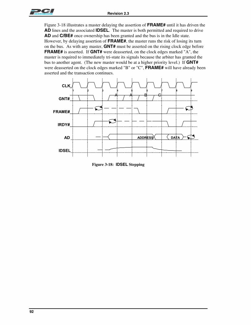
Revision 2.3
92
Figure 3-18 illustrates a master delaying the assertion of FRAME# until it has driven theAD lines and the associated IDSEL. The master is both permitted and required to driveAD and C/BE# once ownership has been granted and the bus is in the Idle state.However, by delaying assertion of FRAME#, the master runs the risk of losing its turnon the bus. As with any master, GNT# must be asserted on the rising clock edge beforeFRAME# is asserted. If GNT# were deasserted, on the clock edges marked "A", themaster is required to immediately tri-state its signals because the arbiter has granted thebus to another agent. (The new master would be at a higher priority level.) If GNT#were deasserted on the clock edges marked "B" or "C", FRAME# will have already beenasserted and the transaction continues.
CLK1 2 3 4 5 7 8 96
GNT#
FRAME#
IRDY#
A A CB
AD
IDSEL
ADDRESS DATA
Figure 3-18: IDSEL Stepping

Revision 2.3
93
3.6.4. Interrupt Acknowledge
The PCI bus supports an Interrupt Acknowledge cycle as shown in Figure 3-19. Thisfigure illustrates an x86 Interrupt Acknowledge cycle on PCI where a single byte enableis asserted and is presented only as an example. In general, the byte enables determinewhich bytes are involved in the transaction. During the address phase, AD[31::00] donot contain a valid address but must be driven with stable data, PAR is valid, and paritymay be checked. An Interrupt Acknowledge transaction has no addressing mechanismand is implicitly targeted to the interrupt controller in the system. As defined in the PCI-to-PCI Bridge Architecture Specification, the Interrupt Acknowledge command is notforwarded to another PCI segment. The Interrupt Acknowledge cycle is like any othertransaction in that DEVSEL# must be asserted one, two, or three clocks after theassertion of FRAME# for positive decode and may also be subtractively decoded by astandard expansion bus bridge. Wait states can be inserted and the request can beterminated, as discussed in Section 3.3.3.2. The vector must be returned when TRDY# isasserted.
FRAME#
CLK
TRDY#
IRDY#
AD
C/BE#
1 2 3 4 5
VECTOR
BE#'s (1110)INT-ACK
NOTVALID
Figure 3-19: Interrupt Acknowledge Cycle
Unlike the traditional 8259 dual cycle acknowledge, PCI runs a single cycleacknowledge. Conversion from the processor's two cycle format to the PCI one cycleformat is easily done in the bridge by discarding the first Interrupt Acknowledge requestfrom the processor.
3.7. Error Functions PCI provides for parity and other system errors to be detected and reported. A singlesystem may include devices that have no interest in errors (particularly parity errors) andagents that detect, signal, and recover from errors. PCI error reporting allows agents thatrecover from parity errors to avoid affecting the operation of agents that do not. To allowthis range of flexibility, the generation of parity is required on all transactions by allagents. The detection and reporting of errors is generally required, with limitedexclusions for certain classes of PCI agents as listed in Section 3.7.2.

Revision 2.3
94
3.7.1. Parity Generation
Parity on PCI provides a mechanism to determine for each transaction if the master issuccessful in addressing the desired target and if data transfers correctly between them.To ensure that the correct bus operation is performed, the four command lines areincluded in the parity calculation. To ensure that correct data is transferred, the four byteenables are also included in the parity calculation. The agent that is responsible fordriving AD[31::00] on any given bus phase is also responsible for driving even parityon PAR. The following requirements also apply when the 64-bit extensions are used(refer to Section 3.8. for more information).
During address and data phases, parity covers AD[31::00] and C/BE[3::0]# linesregardless of whether or not all lines carry meaningful information. Byte lanes notactually transferring data are still required to be driven with stable (albeit meaningless)data and are included in the parity calculation. During configuration, Special Cycle orInterrupt Acknowledge transactions some (or all) address lines are not defined but arerequired to be driven to stable values and are included in the parity calculation.
Parity is generated according to the following rules:
• Parity is calculated the same on all PCI transactions regardless of the type or form.
• The number of "1"s on AD[31::00], C/BE[3::0]#, and PAR equals an evennumber.
• Parity generation is not optional; it must be done by all PCI-compliant devices.
On any given bus phase, PAR is driven by the agent that drives AD[31::00] and lagsthe corresponding address or data by one clock. Figure 3-20 illustrates both read andwrite transactions with parity. The master drives PAR for the address phases on clocks3 and 7. The target drives PAR for the data phase on the read transaction (clock 5) andthe master drives PAR for the data phase on the write transaction (clock 8). Note: Otherthan the one clock lag, PAR behaves exactly like AD[31::00] including wait states andturnaround cycles.
FRAME#
CLK
AD ADDRESS
1 2 3 4 5 6 7 8 9
DATA ADDRESS DATA
PAR
PERR#
Figure 3-20: Parity Operation
Revision 2.3
95
3.7.2. Parity Checking
Parity must be checked to determine if the master successfully addressed the desiredtarget and if data transferred correctly. All devices are required to check parity, exceptdevices in the following two classes for which parity checking is optional:
• Devices that are designed exclusively for use on the system board; e.g., chip sets.System vendors have control over the use of these devices since they will neverappear on add-in cards.
• Devices that never deal with or contain or access any data that represents permanentor residual system or application state; e.g., human interface and video/audio devices.These devices only touch data that is a temporary representation (e.g., pixels) ofpermanent or residual system or application state. Therefore, they are not prone tocreate system integrity problems in the event of undetected failure.
3.7.3. Address Parity Errors
A device is said to have detected an address parity error if the device’s parity checkinglogic detects an error in a single address cycle or either address phase of a dual addresscycle.
If a device detects an address parity error, in some cases, it will assert SERR# (refer toSection 3.7.4.2.), and in all cases it will set the Detected Parity Error bit (Status register,bit 15) (refer to Section 3.7.4.4.).
If a device detects an address parity error, and the device’s Parity Error Response bit(Command register, bit 6) is set, and the device’s address decoder indicates that thedevice is selected, the device must do one of the following:
• claim the transaction and terminate it as if there was no address/command error.
• claim the transaction and terminate with Target-Abort.
• not claim the transaction and let it terminate with Master-Abort.
An error in the address phase of a transaction may affect any or all of the address bits, thecommand bits, and the parity bit. Since devices monitoring the transaction cannotdetermine which bits are actually in error, use of a transaction that contained an addressparity error may cause unpredictable results.
The target is not allowed to claim a transaction and terminate it with Retry solely becauseof an address parity error or a write21 data parity error. However, the occurrence of aparity error does not prevent the target from terminating the transaction with Retry forother reasons.
3.7.4. Error Reporting
PCI provides for the detection and signaling of two kinds of errors: data parity errors andother system errors. It is intended that data parity errors be reported up through theaccess and device driver chain whenever possible. This error reporting chain from targetto bus master to device driver to device manager to operating system is intended to allowerror recovery options to be implemented at any level. Since it is generally not possible
21 Targets check data parity only on write transactions.
Revision 2.3
96
to associate system errors with a specific access chain, they are reported via a separatesystem error signal (refer to Section 3.7.4.2.).
PCI devices are enabled to report data parity errors by the Parity Error Response bit (bit 6of the Command register). This bit is required in all devices except those not required tocheck parity (refer to Section 3.7.2.). If the Parity Error Response bit is set, devices mustrespond to and report data parity errors for all bus operations (except those that occurduring a Special Cycle transaction). If the Parity Error Response bit is cleared, an agentthat detects a data parity error must ignore the error and complete the transaction asthough parity was correct. In this case, no special handling of the data parity error canoccur.
Two signals (pins) and two status bits are used in the PCI error reporting scheme. Eachwill be discussed separately.
3.7.4.1. Data Parity Error Signaling on PERR#
PERR# is used for signaling data parity errors on all transactions except Special Cycletransactions. Data parity errors that occur during a Special Cycle transaction are reportedon SERR# as described in Section 3.7.4.2. PERR# is required for all devices exceptthose not required to check parity (refer to Section 3.7.2.).
If parity error response is enabled (bit 6 of the Command register is set) and a data parityerror is detected by a master during a read transaction, the master must assert PERR#.If parity error response is enabled (bit 6 of the Command register is set) and a data parityerror is detected by a target during a write transaction, the target must assert PERR#.Masters use this information to record the occurrence of the error for the device driver.PERR# is both an input and output signal for a master and only an output signal for atarget.
A device asserting PERR# must do so two clocks after the completion of a data phase inwhich an error occurs, as shown in Figure 3-20. If the receiving agent inserts wait states,that agent is permitted to assert PERR# as soon as a data parity error is detected. Inother words, if the target is inserting wait states during a write transaction, the target ispermitted to assert PERR# two clocks after data is valid (IRDY# asserted) but beforethe data transfers (TRDY# is also asserted). If the master is inserting wait states duringa read transaction, the master is permitted to assert PERR# two clocks after data is valid(TRDY# is asserted) but before the data transfers (IRDY# is also asserted). OncePERR# is asserted, it must remain asserted until two clocks following the completion ofthe data phase (IRDY# and TRDY# both asserted). Note that the master is required toprovide valid byte enables during every clock cycle of every data phase for both read andwrite transactions independent of IRDY#.
If a master asserts PERR# prior to completion of a read data phase, it must eventuallyassert IRDY# to complete the data phase. If a target asserts PERR# prior to completionof a write data phase, it must eventually assert TRDY# to complete the data phase. Thetarget cannot terminate the data phase by signaling Retry, Disconnect without data, orTarget-Abort after signaling PERR#. A master knows a data parity error occurred on awrite data phase anytime PERR# is asserted, which may be prior to the completion ofthe data phase. But the master only knows the data phase was error free two clocksfollowing the completion of the data phase.
Both masters and targets are permitted either to continue a burst transaction or stop itafter detecting a data parity error. During a burst transaction in which multiple data

Revision 2.3
97
phases are completed without intervening wait states, PERR# will be qualified onmultiple consecutive clocks accordingly and may be asserted in any or all of them.
PERR# is a sustained tri-state signal that is bused to all PCI agents. It must be activelydriven to the correct value on each qualified clock edge by the agent receiving the data.At the end of each bus operation, PERR# must actively be driven high for one clockperiod by the agent receiving data, starting two clocks after the AD bus turnaround cycle(e.g., clock 7 in Figure 3-20). The PERR# turnaround cycle occurs one clock later(clock 8 in Figure 3-20). PERR# cannot be driven (enabled) for the current transactionuntil at least three clocks after the address phase (which is one clock long for singleaddress cycles and two clocks long for dual address cycles). Note that the target of awrite transaction must not drive any signal until after asserting DEVSEL#; for example,for decode speed “slow” the target must not drive PERR# until four clocks after theaddress phase.
3.7.4.2. Other Error Signaling on SERR#
If a device is enabled to assert SERR# (i.e., SERR# Enable, bit 8 of the Commandregister, is set), and the device’s Parity Error Response bit (Command register, bit 6) isset, the device must assert SERR# if any of the following conditions occurs:
• The device’s parity checking logic detects an error in a single address cycle or eitheraddress phase of a dual address cycle (regardless of the intended target).
• The device monitors Special Cycle transactions, and the Special Cycles bit(Command register, bit 3) is set, and the device’s parity checking logic detects a dataparity error.
Refer to Section 6.8.2.1. for the cases in which a device must assert SERR# if thatdevice is the master of a Message Signaled Interrupt transaction resulting in PERR#assertion, a Master-Abort, or a Target-Abort.
SERR# may optionally be used to report other internal errors that might jeopardizesystem or data integrity. It must be assumed, however, that signaling on SERR# willgenerate a critical system interrupt (e.g., NMI or Machine Check) and is, therefore, fatal.Consequently, care should be taken in using SERR# to report non-parity or systemerrors.
SERR# is required for all devices except those not required to check parity (refer toSection 3.7.2.). SERR# is an open drain signal that is wire-ORed with all other PCIagents and, therefore, may be simultaneously driven by multiple agents. An agentreporting an error on SERR# drives it active for a single clock and then tri-states it.(Refer to Section 2.2.5. for more details.) Since open drain signaling cannot guaranteestable signals on every rising clock edge, once SERR# is asserted its logical value mustbe assumed to be indeterminate until the signal is sampled in the deasserted state on atleast two successive rising clock edges.

Revision 2.3
98
3.7.4.3. Master Data Parity Error Status Bit
The Master Data Parity Error bit (Status register, bit 8) must be set by the master if itsParity Error Response bit (Command register, bit 6) is set and either of the following twoconditions occurs:
• The master detects a data parity error on a read transaction.
• The master samples PERR# asserted on a write transaction.
If the Parity Error Response bit is cleared, the master must not set the Master Data ParityError bit, even if the master detects a parity error or the target asserts PERR#.
Targets never set the Master Data Parity Error bit.
3.7.4.4. Detected Parity Error Status Bit
The Detected Parity Error bit (Status register, bit 15) must be set by a device whenever itsparity checking logic detects a parity error, regardless of the state the Parity ErrorResponse bit (bit 6 of the command register). The Detected Parity Error bit is required tobe set by the device when any of the following conditions occurs:
• The device’s parity checking logic detects an error in a single address cycle or eitheraddress phase of a dual address cycle.
• The device’s parity checking logic detects a data parity error and the device is thetarget of a write transaction.
• The device’s parity checking logic detects a data parity error and the device is themaster of a read transaction.
3.7.5. Delayed Transactions and Data Parity Errors
This section presents additional requirements for error handling that are unique to a targetcompleting a transaction as a Delayed Transaction. Data parity error requirementspresented in previous sections apply to Delayed Transactions as well.
A data parity error can occur during any of the three steps of a Delayed Transaction, themaster request step, the target completion step, or the master completion step (refer toSection 3.3.3.3.1.). The requirements for handling the error vary depending upon thestep in which the error occurred. Errors that occur during the target completion phase arespecific to the target device and are handled in a device-specific manner (not specifiedhere). 22 Device behavior for errors that occur during the master request step or mastercompletion step depend upon whether the Delayed Transaction is a read23 or a write24
transaction.
22 If the actual target resides on a PCI bus segment generated by a PCI-to-PCI bridge, the target completionphase occurs across a PCI bus segment. In this case, the PCI-to-PCI Bridge Architecture Specificationdetails additional requirements for error handling during the target completion phase of a read DelayedTransaction.
23 Memory Read, Memory Read Line, Memory Read Multiple, Configuration Read, I/O Read, or InterruptAcknowledge.
24 Configuration Write or I/O Write, but never Memory Write and Invalidate or Memory Write.

Revision 2.3
99
During a read transaction, the target device sources the data, and parity is not valid untilTRDY# is asserted. Therefore, a data parity error cannot occur during the masterrequest phase or any subsequent reattempt by the master that is terminated with Retry.During the master completion step of read transaction, the target sources data and dataparity and the master checks parity and conditionally asserts PERR# as for any other(not delayed) transaction (refer to Section 3.7.4.).
During a write transaction, the master sources the write data and must assert IRDY#when the data is valid independent of the response by the target device (refer toSection 3.2.1.). Therefore, a data parity error may occur both in the master request andthe master completion steps. In addition, it is possible for a data parity error to be eitherconstant (i.e., the same error occurs each time the master repeats the transaction) ortransient (i.e., the error occurs on some but not other repetitions of the transaction by themaster). The data parity error reporting methods for write Delayed Transactionsdescribed in the following sections are designed to detect and report both constant andtransient data parity errors, and to prevent transient data parity errors from causing adeadlock condition.
If a target detects a data parity error on a write transaction that would otherwise havebeen handled as a Delayed Transaction, the target is required to do the following:
1. Complete the data phase in which the error occurred by asserting TRDY#. If themaster is attempting a burst, the target must also assert STOP#.
2. Report the error as described in Section 3.7.4.1.
3. Discard the transaction. No Delayed Write Request is enqueued, and no DelayedWrite Completion is retired.
If the target detects a data parity error during the initial request phase of a Delayed WriteTransaction, no Delayed Request is ever enqueued.
If the target enqueues a good Delayed Write Request and later detects a data parity errorduring a subsequent repetition of the transaction, the target does not retire any DelayedWrite Completions, even if the transaction appears to match one previously enqueued. (Itis impossible to determine whether the transaction really matches a previously enqueuedone, since an error is present.) This causes the target to have an orphan Delayed WriteCompletion, because the master believes the transaction has completed, but the target iswaiting for the original (error free) request to be repeated. The orphan completion isdiscarded when the target’s Discard Timer expires (refer to Section 3.3.3.3.3.). Whilewaiting for the discard timer to expire, some target implementations will not be able toaccept a new Delayed Transaction, since the target is not required to handle multipleDelayed Transactions at the same time. However, since this condition is temporary, adeadlock cannot occur. While in this condition, the device is required to completetransactions that use memory write25 commands (refer to Section 3.3.3.3.4.).
25 This includes two commands: Memory Write and Invalidate and Memory Write.

Revision 2.3
100
3.7.6. Error Recovery
The action that a system takes as a result of the assertion of SERR# is not controlled bythis specification. The assertion of SERR# by a device indicates that the device hasencountered an error from which it cannot recover. The system may optionally stopexecution at that point, if it does not have enough information to contain and recoverfrom the error condition.
The PCI parity error signals and status bits are designed to provide a method for dataparity errors to be detected and reported (if enabled). On a write transaction, the targetalways signals data parity errors back to the master on PERR#. On a read transaction,the master asserts PERR# to indicate to the system that an error was detected. In bothcases, the master has the ability to promote the error to its device driver or the operatingsystem or to attempt recovery using hardware and/or software methods.
The system designer may elect to report all data parity errors to the operating system byasserting SERR# when the central resource samples PERR# asserted. Note that whenthis option is used, recovery is not possible.
Implementation Note: Recovery from Data Parity ErrorsIt is optional for PCI masters and systems to attempt recovery from data parity errors.The following are examples of how data parity error recovery may be attempted:
• Recovery by the master. If the master of the transaction in which the parity errorwas detected has sufficient knowledge that the transaction can be repeated withoutside-effects, then the master may simply repeat the transaction. If no error occurs onthe repeated transaction, reporting of the parity error (to the operating system ordevice driver) is unnecessary. If the error persists, or if the master is not capable ofrecovering from the data parity error, the master must inform its device driver. Thiscan be accomplished by generating an interrupt, modifying a status register, setting aflag, or other suitable means. When the master does not have a device driver, it mayreport the error by asserting SERR#.
Note: Most devices have side-effects when accessed, and, therefore, it is unlikelythat recovery is possible by simply repeating a transaction. However, in applicationswhere the master understands the behavior of the target, it may be possible to recoverfrom the error by repetition of the transaction.
• Recovery by the device driver. The device driver may support an error recoverymechanism such that the data parity error can be corrected. In this case, the reportingof the error to the operating system is not required. For example, the driver may beable to repeat an entire block transfer by reloading the master with the transfer size,source, and destination addresses of the data. If no error occurs on the repeated blocktransfer, then the error is not reported. When the device driver does not havesufficient knowledge that the access can be repeated without side-effects, it mustreport the error to the operating system.
• Recovery (or error handling) by the operating system. Once the data parity errorhas been reported to the operating system, no other agent or mechanism can recoverfrom the error. How the operating system handles the data parity error is operatingsystem dependent.
Revision 2.3
101
3.8. 64-Bit Bus ExtensionPCI supports a high 32-bit bus, referred to as the 64-bit extension to the standard low32-bit bus. The 64-bit bus provides additional data bandwidth for agents that require it.The high 32-bit extension for 64-bit devices needs an additional 39 signal pins:REQ64#, ACK64#, AD[63::32], C/BE[7::4]#, and PAR64. These signals are definedin Section 2.2.8. 32-bit agents work unmodified with 64-bit agents. 64-bit agents mustdefault to 32-bit mode unless a 64-bit transaction is negotiated. Hence, 64-bittransactions are totally transparent to 32-bit devices. Note: 64-bit addressing does notrequire a 64-bit data path (refer to Section 3.9.).
64-bit transactions on PCI are dynamically negotiated (once per transaction) between themaster and target. This is accomplished by the master asserting REQ64# and the targetresponding to the asserted REQ64# by asserting ACK64#. Once a 64-bit transaction isnegotiated, it holds until the end of the transaction. ACK64# must not be asserted unlessREQ64# was sampled asserted during the same transaction. REQ64# and ACK64# areexternally pulled up to ensure proper behavior when mixing 32- and 64-bit agents. Referto Section 3.8.1. for the operation of 64-bit devices in a 32-bit system.
During a 64-bit transaction, all PCI protocol and timing remain intact. Only memorytransactions make sense when doing 64-bit data transfers. Interrupt Acknowledge andSpecial Cycle26 commands are basically 32-bit transactions and must not be used with aREQ64#. The bandwidth requirements for I/O and configuration transactions cannotjustify the added complexity, and, therefore, only memory transactions support 64-bitdata transfers.
All memory transactions and other bus transfers operate the same whether data istransferred 32 or 64 bits at a time. 64-bit agents can transfer from one to eight bytes perdata phase, and all combinations of byte enables are legal. As in 32-bit mode, byteenables may change on every data phase. The master initiating a 64-bit data transactionmust use a double DWORD (Quadword or 8 byte) referenced address (AD[2] must be"0" during the address phase).
When a master requests a 64-bit data transfer (REQ64# asserted), the target has threebasic responses and each is discussed in the following paragraphs.
1. Complete the transaction using the 64-bit data path (ACK64# asserted).
2. Complete the transaction using the 32-bit data path (ACK64# deasserted).
3. Complete a single 32-bit data transfer (ACK64# deasserted, STOP# asserted).
The first option is where the target responds to the master that it can complete thetransaction using the 64-bit data path by asserting ACK64#. The transaction thentransfers data using the entire data bus and up to 8 bytes can be transferred in each dataphase. It behaves like a 32-bit bus except more data transfers each data phase.
The second option occurs when the target cannot perform a 64-bit data transfer to theaddressed location (it may be capable in a different space). In this case, the master isrequired to complete the transaction acting as a 32-bit master and not as a 64-bit master.The master has two options when the target does not respond by asserting ACK64# whenthe master asserts REQ64# to start a write transaction. The first option is that the masterquits driving the upper AD lines and only provides data on the lower 32 AD lines. Thesecond option is the master continues presenting the full 64 bits of data on each even
26 Since no agent claims the access by asserting DEVSEL# and, therefore, cannot respond with ACK64#.

Revision 2.3
102
DWORD address boundary. On the odd DWORD address boundary, the master drivesthe same data on both the upper and lower portions of the bus.
The third and last option is where the target is only 32 bits and cannot sustain a burst forthis transaction. In this case, the target does not respond by asserting ACK64#, butterminates the transaction by asserting STOP#. If this is a Retry termination (STOP#asserted and TRDY# deasserted) the master repeats the same request (as a 64-bit request)at a later time. If this is a Disconnect termination (STOP# and TRDY# asserted), themaster must repeat the request as a 32-bit master since the starting address is now on aodd DWORD boundary. If the target completed the data transfer such that the nextstarting address would be a even DWORD boundary, the master would be free to requesta 64-bit data transfer. Caution should be used when a 64-bit request is presented and thetarget transfers a single DWORD as a 32-bit agent. If the master were to continue theburst with the same address, but with the lower byte enables deasserted, no forwardprogress would be made because the target would not transfer any new data, since thelower byte enables are deasserted. Therefore, the transaction would continue to berepeated forever without making progress.
64-bit parity (PAR64) works the same for the high 32-bits of the 64-bit bus as the 32-bitparity (PAR) works for the low 32-bit bus. PAR64 covers AD[63::32] andC/BE[7::4]# and has the same timing and function as PAR. (The number of "1"s onAD[63::32], C/BE[7::4]#, and PAR64 equal an even number). PAR64 must be validone clock after each address phase on any transaction in which REQ64# is asserted. (All64-bit targets qualify address parity checking of PAR64 with REQ64#.) 32-bit devicesare not aware of activity on 64-bit bus extension signals.
For 64-bit devices checking parity on data phases, PAR64 must be additionally qualifiedwith the successful negotiation of a 64-bit transaction. PAR64 is required for 64-bit dataphases; it is not optional for a 64-bit agent.
In the following two figures, a 64-bit master requests a 64-bit transaction utilizing asingle address phase. This is the same type of addressing performed by a 32-bit master(in the low 4 GB address space). The first, Figure 3-21, is a read where the targetresponds with ACK64# asserted and the data is transferred in 64-bit data phases. Thesecond, Figure 3-22, is a write where the target does not respond with ACK64# assertedand the data is transferred in 32-bit data phases (the transaction defaulted to 32-bit mode).These two figures are identical to Figures 3-5 and 3-6 except that 64-bit signals havebeen added and in Figure 3-21 data is transferred 64-bits per data phase. The sametransactions are used to illustrate that the same protocol works for both 32- and 64-bittransactions.
AD[63::32] and C/BE[7::4]# are reserved during the address phase of a single addressphase transaction. AD[63::32] contain data and C/BE[7::4]# contain byte enables forthe upper four bytes during 64-bit data phases of these transactions. AD[63::32] andC/BE[7::4]# are defined during the two address phases of a dual address cycle (DAC)and during the 64-bit data phases (refer to Section 3.9. for details).
Figure 3-21 illustrates a master requesting a 64-bit read transaction by asserting REQ64#(which exactly mirrors FRAME#). The target acknowledges the request by assertingACK64# (which mirrors DEVSEL#). Data phases are stretched by both agentsdeasserting their ready lines. 64-bit signals require the same turnaround cycles as their32-bit counterparts.

Revision 2.3
103
FRAME#
CLK
TRDY#
IRDY#
AD[31::00]
DEVSEL#
C/BE[3::0]#
ADDRESS
BUS CMD
DATA-3
BE#'s
1 2 3 4 5 6 7 8 9
DAT
A TR
ANSF
ER
DAT
A T
RAN
SFE
R
DAT
A TR
ANSF
ER
WAI
T
ADDRESSPHASE
DATAPHASE
DATAPHASE
WAI
T
DATAPHASE
WAI
T
DATA-2
BE#'s
DATA-1 DATA-5
DATA-6DATA-4
REQ64#
AD[63::32]
C/BE[7::4]#
ACK64#
Figure 3-21: 64-bit Read Request With 64-bit Transfer
Figure 3-22 illustrates a master requesting a 64-bit transfer. The 32-bit target is notconnected to REQ64# or ACK64#, and ACK64# is kept in the deasserted state with apull-up. As far as the target is concerned, this is a 32-bit transfer. The master convertsthe transaction from 64- to 32-bits. Since the master is converting 64-bit data transfersinto 32-bit data transfers, there may or may not be any byte enables asserted during anydata phase of the transaction. Therefore, all 32-bit targets must be able to handle dataphases with no byte enables asserted. The target should not use Disconnect or Retrybecause a data phase is encountered that has no asserted byte enables, but should assertTRDY# and complete the data phase. However, the target is allowed to use Retry orDisconnect because it is internally busy and unable to complete the data transferindependent of which byte enables are asserted. The master resends the data thatoriginally appeared on AD[63::32] during the first data phase on AD[31::00] during thesecond data phase. The subsequent data phases appear exactly like the 32-bit transfer.(If the 64-bit signals are removed, Figure 3-22 and Figure 3-6 are identical.)

Revision 2.3
104
FRAME#
CLK
TRDY#
IRDY#
AD[31::00]
DEVSEL#
C/BE[3::0]#
ADDRESS
BUS CMD
1 2 3 4 5 6 7 8 9
ADDRESSPHASE
DATAPHASE
DA
TA T
RA
NS
FER
DAT
A TR
ANSF
ER
WA
IT
WA
IT
WAI
T
DAT
A TR
ANSF
ER
DATA-2
DATA-1 DATA-2 DATA-3
C/BE[7::4]#
AD[63::32]
REQ64#
ACK64#
BE#'s-2 BE#'s-3BE#'s-1
BE#'s-2
DATAPHASE
DATAPHASE
Figure 3-22: 64-bit Write Request With 32-bit Transfer
Using a single data phase with 64-bit transfers may not be very effective. Since themaster does not know how the transaction will be resolved with ACK64# untilDEVSEL# is returned, it does not know the clock on which to deassert FRAME# for a64-bit single data phase transaction. IRDY# must remain deasserted until FRAME#signaling is resolved. The single 64-bit data phase may have to be split into two 32-bitdata phases when the target is only 32-bits, which means a two phase 32-bit transfer is atleast as fast as a one phase 64-bit transfer.
3.8.1. Determining Bus Width During System Initialization
REQ64# is used during reset to distinguish between parts that are connected to a 64-bitdata path, and those that are not. PCI add-in card slots that support only a 32-bit datapath must not connect REQ64# to any other slots or devices. (The REQ64# andACK64# pins are located in the 32-bit portion of the connector.) Each 32-bit-onlyconnector must have an individual pull-up resistor for REQ64# on the system board.ACK64# is bused to all 64-bit devices and slots on the system board and pulled up with asingle resistor located on the system board. ACK64# for each 32-bit slots must bedeasserted either by connecting it to the ACK64# signal connecting the 64-bit devicesand slots or by individual pull-up resistors on the system board.
Revision 2.3
105
REQ64# is bused to all devices on the system board (including PCI connector slots) thatsupport a 64-bit data path. This signal has a single pull-up resistor on the system board.The central resource must drive REQ64# low (asserted) during the time that RST# isasserted, according to the timing specification in Section 4.3.2. Devices that seeREQ64# asserted on the rising edge of RST# are connected to the 64-bit data path, andthose that do not see REQ64# asserted are not connected. This information may be usedby the component to stabilize floating inputs during runtime, as described below.
REQ64# has setup and hold time requirements relative to the deasserting (high-going)edge of RST#. While RST# is asserted, REQ64# is asynchronous with respect to CLK.
When a 64-bit data path is provided, AD[63::32], C/BE[7::4]#, and PAR64 requireeither pull-up resistors or input "keepers," because they are not used in transactions with32-bit devices and may, therefore, float to the threshold level causing oscillation or highpower drain through the input buffer. This pull-up or keeper function must be part of thesystem board central resource, not the add-in card, (refer to Section 4.3.3.) to ensure aconsistent solution and avoid pull-up current overload.
When the 64-bit data path is present on a device but not connected (as in a 64-bit add-incard plugged into a 32-bit PCI slot), that PCI device must insure that its inputs do notoscillate, and that there is not a significant power drain through the input buffer bothbefore and after the rising edge of RST#. This can be done in a variety of ways; e.g.,biasing the input buffer or actively driving the outputs continuously (since they are notconnected to anything). External resistors on an add-in card or any solution that violatesthe input leakage specification are prohibited.
While RST# is asserted, the PCI device floats its output buffers for the extended datapath, AD[63::32], C/BE[7::4]#, and PAR64, unless the device input buffers cannottolerate their inputs floating for an indefinitely long RST# period. If the device inputbuffers cannot tolerate this, the component must control its inputs while RST# isasserted. In this case, the device is permitted to enable its outputs continuously whileRST# is asserted and REQ64# is deasserted (indicating a 32-bit bus), but must drivethem to a logic low level (in case the bus connection is actually 64-bits wide andREQ64# has not yet settled to its final value). After the device detects that REQ64# isdeasserted at the rising edge of RST#, the device must continue to control the extendedbus to protect the device input buffers.
3.9. 64-bit AddressingPCI supports memory addressing beyond the low 4 GB by defining a mechanism totransfer a 64-bit address from the master of the transaction to the target. No additionalpins are required for a 32- or 64-bit device to support 64-bit addressing. Devices thatsupport only 32-bit addresses are mapped into the low 4 GB of the address space andwork transparently with devices that generate 64-bit addresses. Only memorytransactions support 64-bit addressing.
The width of the address is independent of the width of the bus on either the master or thetarget. If both the master and target support a 64-bit bus, the entire 64-bit address couldtheoretically be provided in a single clock. However, the master is required in all cases touse two clocks to communicate a 64-bit address, since the width of the target’s bus is notknown during the address phase.
The standard PCI bus transaction supports a 32-bit address, Single Address Cycle (SAC),where the address is valid for a single clock when FRAME# is first sampled asserted. Tosupport the transfer of a 64-bit address, a Dual Address Cycle (DAC) bus command isused, accompanied with one of the defined bus commands to indicate the desired data

Revision 2.3
106
phase activity for the transaction. The DAC uses two clocks to transfer the entire 64-bitaddress on the AD[31::00] signals. When a 64-bit master uses DAC (64-bit addressing),it must provide the upper 32 bits of the address on AD[63::32] and the associatedcommand for the transaction on C/BE[7::4]# during both address phases of thetransaction to allow 64-bit targets additional time to decode the transaction.
Figure 3-23 illustrates a DAC for a read transaction. In a basic SAC read transaction, aturnaround cycle follows the address phase. In the DAC read transaction, an additionaladdress phase is inserted between the standard address phase and the turnaround cycle.In the figure, the first and second address phases occur on clock 2 and 3 respectively.The turnaround cycle between the address and data phases is delayed until clock 4. Note:FRAME# must be asserted during both address phases even for nonbursting single dataphase transactions. To adhere to the FRAME# - IRDY# relationship, FRAME# cannotbe deasserted until IRDY# is asserted. IRDY# cannot be asserted until the masterprovides data on a write transaction or is ready to accept data on a read transaction.
A DAC is decoded by a potential target when a "1101" is present on C/BE[3::0]# duringthe first address phase. If a 32-bit target supports 64-bit addressing, it stores the addressthat was transferred on AD[31::00] and prepares to latch the rest of the address on thenext clock. The actual command used for the transaction is transferred during the secondaddress phase on C/BE[3::0]#. A 64-bit target is permitted to latch the entire address onthe first address phase. Once the entire address is transferred and the command islatched, the target determines if DEVSEL# is to be asserted. The target can do fast,medium, or slow decode one clock delayed from SAC decoding. A subtractive decodeagent adjusts to the delayed device selection timing either by ignoring the entiretransaction or by delaying its own assertion of DEVSEL#. If the bridge does support 64-bit addressing, it will delay asserting its DEVSEL# (if it does support 64-bit addressing).The master (of a DAC) will also delay terminating the transaction with Master-Abort forone additional clock.
The execution of an exclusive access is the same for either DAC or SAC. In either case,LOCK# is deasserted during the address phase (first clock) and asserted during thesecond clock (which is the first data phase for SAC and the second address phase for aDAC). Agents monitoring the transaction understand the lock resource is busy, and thetarget knows the master is requesting a locked operation. For a target that supports bothSAC and DAC, the logic that handles LOCK# is the same.
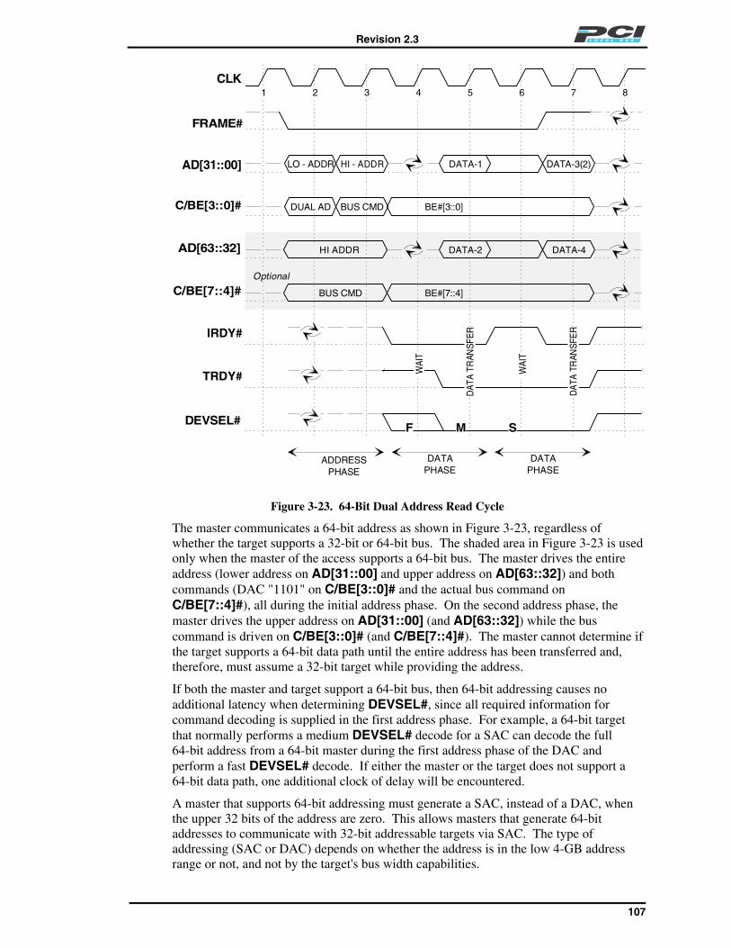
Revision 2.3
107
FRAME#
CLK
TRDY#
IRDY#
AD[31::00]
DEVSEL#
C/BE[3::0]# BUS CMD BE#[3::0]
1 2 3 4 5 6 7 8
ADDRESSPHASE
DATAPHASE
DATAPHASE
DATA-2
BE#[7::4]
DATA-4AD[63::32]
C/BE[7::4]#
HI - ADDRLO - ADDR DATA-3(2)DATA-1
HI ADDR
DUAL AD
BUS CMD
WAI
T
F M S
DAT
A TR
ANSF
ER
DA
TA T
RAN
SFE
R
Optional
WAI
T
Figure 3-23. 64-Bit Dual Address Read Cycle
The master communicates a 64-bit address as shown in Figure 3-23, regardless ofwhether the target supports a 32-bit or 64-bit bus. The shaded area in Figure 3-23 is usedonly when the master of the access supports a 64-bit bus. The master drives the entireaddress (lower address on AD[31::00] and upper address on AD[63::32]) and bothcommands (DAC "1101" on C/BE[3::0]# and the actual bus command onC/BE[7::4]#), all during the initial address phase. On the second address phase, themaster drives the upper address on AD[31::00] (and AD[63::32]) while the buscommand is driven on C/BE[3::0]# (and C/BE[7::4]#). The master cannot determine ifthe target supports a 64-bit data path until the entire address has been transferred and,therefore, must assume a 32-bit target while providing the address.
If both the master and target support a 64-bit bus, then 64-bit addressing causes noadditional latency when determining DEVSEL#, since all required information forcommand decoding is supplied in the first address phase. For example, a 64-bit targetthat normally performs a medium DEVSEL# decode for a SAC can decode the full64-bit address from a 64-bit master during the first address phase of the DAC andperform a fast DEVSEL# decode. If either the master or the target does not support a64-bit data path, one additional clock of delay will be encountered.
A master that supports 64-bit addressing must generate a SAC, instead of a DAC, whenthe upper 32 bits of the address are zero. This allows masters that generate 64-bitaddresses to communicate with 32-bit addressable targets via SAC. The type ofaddressing (SAC or DAC) depends on whether the address is in the low 4-GB addressrange or not, and not by the target's bus width capabilities.
Revision 2.3
108
A 64-bit addressable target must act like a 32-bit addressable target (respond to SACtransactions) when mapped in the lower 4 GB address space. If a 32-bit master mustaccess targets mapped above the lower 4 GB address space, that master must support64-bit addressing using DAC.
3.10. Special Design ConsiderationsThis section describes topics that merit additional comments or are related to PCI but arenot part of the basic operation of the bus.
1. Third party DMAThird party DMA is not supported on PCI since sideband signals are not supportedon the connector. The intent of PCI is to group together the DMA function indevices that need master capability and, therefore, third party DMA is not supported.
2. Snooping PCI transactionsAny transaction generated by an agent on PCI may be snooped by any other agent onthe same bus segment. Snooping does not work when the agents are on different PCIbus segments. In general, the snooping agent cannot drive any PCI signal, but mustbe able to operate independently of the behavior of the current master or target.
3. Illegal protocol behaviorA device is not encouraged actively to check for protocol errors. However, if adevice does detect illegal protocol events (as a consequence of the way it isdesigned), the design may return its state machines (target or master) to an Idle stateas quickly as possible in accordance with the protocol rules for deassertion and tri-state of signals driven by the device.
4. VGA palette snoopThe active VGA device always responds to a read of the color palette, while eitherthe VGA or graphics agent will be programmed to respond to write transactions tothe color palette and the other will snoop it. When a device (VGA or graphics) hasbeen programmed to snoop a write to the VGA palette register, it must only latch thedata when IRDY# and TRDY# are both asserted on the same rising clock edge orwhen a Master-Abort occurs. The first option is the normal case when a VGA andgraphics device are present in the same system. The second option occurs when nodevice on the current bus has been programmed to positively respond to this range ofaddresses. This occurs when the PCI segment is given the first right of refusal and asubtractive decode device is not present. In some systems, this access is stillforwarded to another bus which will complete the access. In this type of system, adevice that has been programmed to snoop writes to the palette should latch the datawhen the transaction is terminated with Master-Abort.
The palette snoop bit will be set by the system BIOS when it detects both a VGAdevice and a graphics accelerator device that are on separate add-in cards on the samebus or on the same path but on different buses.
• When both agents are PCI devices that reside on the same bus, either device canbe set to snoop and the other will be set to positively respond.
• When both are PCI devices that reside on different buses but on the same path,the first device found in the path will be set to snoop and the other device may beset to positively respond or snoop the access. (Either option works in a PC-ATcompatible system since a write transaction on a PCI segment, other than theprimary PCI bus, that is terminated with Master-Abort is simply terminated andthe data is dropped and Master-Aborts are not reported.)

Revision 2.3
109
• When one device is on PCI and the other is behind the subtractive decode device,the PCI device will be set to snoop and the subtractive decode device willautomatically claim the access and forward it.
The only case where palette snooping would be turned off is when only a VGAdevice (no graphics device) is present in the system, or both the VGA and graphicsdevices are integrated together into single device or add-in card.
Note: Palette snooping does not work when the VGA and graphics devices reside ondifferent buses that are not on the same path. This occurs because only a single agentper bus segment may claim the access. Therefore, one agent will never see the accessbecause its bridge cannot forward the access. When a device has been programmedto snoop the access, it cannot insert wait states or delay the access in any way and,therefore, must be able to latch and process the data without delay.
For more information on PCI support of VGA devices, refer to Appendix A of thePCI-to-PCI Bridge Architecture Specification.
5. Potential deadlock scenario when using PCI-to-PCI bridgesWarning: A potential deadlock will occur when all the following conditions exist ina system:
1. When PCI-to-PCI bridges are supported in the system. (Note: If an add-in cardconnector is supported, PCI-to-PCI bridges may be present in the system.)
2. A read access originated by the host bridge targets a PCI device that requiresmore than a single data phase to complete. (Eight-byte transfer or an access thatcrosses a DWORD boundary when targeting an agent that responds to thisrequest as 32-bit agent or resides on a 32-bit PCI segment.)
The deadlock occurs when the following steps are met:
1. A burst read is initiated on PCI by the host bridge and only the first data phasecompletes. (This occurs because either the target or the PCI-to-PCI bridge in thepath terminates the request with Disconnect.)
2. The request passes through a PCI-to-PCI bridge and the PCI-to-PCI bridgeallows posted write data (moving toward main memory) after the initial readcompletes.
3. The host bridge that originated the read request blocks the path to main memory.
The deadlock occurs because the PCI-to-PCI bridge cannot allow a read to transverseit while holding posted write data. The host bridge that initiated the PCI accesscannot allow the PCI-to-PCI bridge to flush data until it completes the second read,because there is no way to “back-off” the originating agent without losing data. Itmust be assumed the read data was obtained from a device that has destructive readside-effects. Therefore, discarding the data and repeating the access is not an option.
If all these conditions are met, the deadlock will occur. If the system allows all theconditions to exist, then the host bridge initiating the read request must use LOCK#to guarantee that the read access will complete without the deadlock conditions beingmet. The fact that LOCK# is active for the transaction causes the PCI-to-PCI bridgeto turn-off posting until the lock operation completes. (A locked operation completeswhen LOCK# is deasserted while FRAME# is deasserted.)
Note: The use of LOCK# is only supported by PCI-to-PCI bridges movingdownstream (away from the processor). Therefore, this solution is only applicable tohost bus bridges.

Revision 2.3
110
Another deadlock that is similar to the above deadlock occurs doing an I/O Writeaccess that straddles an odd DWORD boundary. The same condition occurs as theread deadlock when the host bridge cannot allow access to memory until the I/Owrite completes. However, LOCK# cannot be used to prevent this deadlock sincelocked accesses must be initiated with a read access.
6. Potential data inconsistency when an agent uses delayed transaction termination
Delayed Completion transactions on PCI are matched by the target with the requesterby comparing addresses, bus commands, and byte enables, and if a write, write data.As a result, when two masters access the same address with the same bus commandand byte enables, it is possible that one master will obtain the data assuming that it isa read which was actually requested by the other master. In a prefetchable region,this condition can occur even if the byte enables, and in some cases, the commands ofthe two transactions do not match. A prefetchable region can be defined by the targetusing range registers or by the master using the Memory Read Line or Memory ReadMultiple commands. Targets completing read accesses in a prefetchable memoryrange ignore the byte enables and can also alias the memory read commands whencompleting the delayed read request.
If no intervening write occurs between the read issued by the two masters, there is nodata consistency issue. However, if a master completes a memory write and thenrequests a read of the same location, there is a possibility that the read will return asnapshot of that location which actually occurred prior to the write (due to a DelayedRead Request by another master queued prior to the write).
This is only a problem when multiple masters on one side of a bridge are polling thesame location on the other side of the bridge and one of the masters also writes thelocation. Although it is difficult to envision a real application with thesecharacteristics, consider the sequence below:
1. Master A attempts a read to location X and a bridge responds to the request usingDelayed Transaction semantics (queues a Delayed Read Request).
2. The bridge obtains the requested read data and the Delayed Request is nowstored as a Delayed Completion in the bridge.
3. Before Master A is able to complete the read request (obtain the results stored inthe Delayed Completion in the bridge), Master B does a memory write toLocation X and the bridge posts the memory write transaction.
4. Master B then reads location X using the same address, byte enables, and buscommand as Master A’s original request. Note that if the transaction reads froma prefetchable location, the two commands can be confused by the bridge even ifthe byte enable patterns and read commands are different.
5. The bridge completes Master B’s read access and delivers read data which is asnapshot of Location X prior to the memory write of Location X by Master B.
Since both transactions are identical, the bridge provides the data to the wrongmaster. If Master B takes action on the read data, then an error may occur, sinceMaster B will see the value before the write. However, if the purpose of the read byMaster B was to ensure that the write had completed at the destination, no erroroccurs and the system is coherent since the read data is not used (dummy read). Ifthe purpose of the read is only to flush the write posted data, it is recommended thatthe read be to a different DWORD location of the same device. Then the reading ofstale data does not exist. If the read is to be compared to decide what to do, it isrecommended that the first read be discarded and the decision be based on the secondread.

Revision 2.3
111
The above example applies equally to an I/O controller that uses Delayed Transactiontermination. In the above example, replace the word "bridge" with "I/O controller"and the same potential problem exists.
A similar problem can occur if the two masters are not sharing the same location, butlocations close to each other, and one master begins reading at a smaller address thanthe one actually needed. If the smaller address coincides exactly with the address ofthe other master’s read from the near location, then the two masters’ reads can beswapped by a device using Delayed Transaction termination. If there is anintervening write cycle, then the second master may receive stale data; i.e., the resultsfrom the read which occurred before the write cycle. The result of this example is thesame as the first example since the start addresses are the same. To avoid thisproblem, the master must address the data actually required and not start at a smalleraddress.
In summary, this problem can only occur if two masters on one side of a bridge aresharing locations on the other side of the bridge. Although typical applications arenot configured this way, the problem can be avoided if a master doing a read fetchesonly the actual data it needs and does not prefetch data before the desired data, or ifthe master does a dummy read after the write to guarantee that the write completes.
Another data inconsistency situation can occur when a single master changes itsbehavior based on a new transaction it receives after having a request terminated withRetry. The following sequence illustrates the data inconsistency:
1. A master is informed that pointer 1 at DWORD Location X is valid. (Pointer 2 atLocation Y, the next sequential DWORD location, is not valid.)
2. The master initiates a memory read to Location X and is terminated with Retry.(The master intends to read only pointer 1, since pointer 2 is invalid.)
3. The host bridge begins to fetch the contents of Location X as a DelayedTransaction.
4. The host bridge completes the read request, prefetching beyond Location X toinclude Location Y and places the Delayed Read Completion in the outboundqueue.
5. The CPU updates pointer 2 in Location Y in memory.
6. The CPU uses a memory write to inform the master that pointer 2 is valid. Thehost bridge posts the memory write. Ordering rule number 7 in Appendix Erequires the host bridge to allow the posted memory write transaction to pass theDelayed Read Completion of Location X (including the stale value fromLocation Y).
7. The host bridge executes the posted memory write on the PCI bus informing themaster that pointer 2 in now valid.
8. The master repeats the original memory read to Location X, but because pointer2 in now valid, it extends the transaction and obtains two DWORDS includingLocation Y.
The data the master received from Location Y is stale. To prevent this datainconsistency from occurring, the master is not allowed to extend a memory readtransaction beyond its original intended limits after it has been terminated withRetry.
7. Peer-to-peer transactions crossing multiple host bridges
Revision 2.3
112
PCI host bridges may, but are not required to, support PCI peer-to-peer transactionsthat traverse multiple PCI host bridges.
8. The effect of PCI-to-PCI bridges on the PCI clock specification
The timing parameters for CLK for PCI add-in card connectors are specified at theinput of the device in the slot. Refer to Section 4.2.3.1. and Section 7.6.4.1. for moreinformation. Like all signals on the connector, only a single load is permitted onCLK in each slot. An add-in card that uses several devices behind a PCI-to-PCIbridge must accommodate the clock buffering requirements of that bridge. Forexample, if the bridge’s clock buffer affects the duty cycle of CLK, the rest of thedevices on the add-in card must accept the different duty cycle. It is theresponsibility of the add-in card designer to choose components with compatibleCLK specifications.
The system must always guarantee the timing parameters for CLK specified inSection 4.2.3.1. and Section 7.6.4.1. at the input of the device in a PCI add-in cardslot, even if the system board places PCI slots on the secondary side of a PCI-to-PCIbridge. It is the responsibility of the system board designer to choose clock sourcesand PCI-to-PCI bridges that will guarantee this specification for all slots.
9. Devices cannot drive and receive signals at the same time
Bus timing requires that no device both drive and receive a signal on the bus at thesame time. System timing analysis considers the worst signal propagation case to bewhen one device drives a signal and the signal settles at the input of all other deviceson the bus. In most cases, the signal will not settle at the driving device until sometime after it has settled at all other devices. Refer to Section 4.3.5. and Section 7.7.5.for a description of Tprop.
Logic internal to a device must never use the signal received from the bus while thatdevice is driving the bus. If internal logic requires the state of a bus signal while thedevice is driving the bus, that logic must use the internal signal (the one going to theoutput buffer of the device) rather than the signal received from the device inputbuffer. For example, if logic internal to a device continuously monitors the state ofFRAME# on the bus, that logic must use the signal from the device input bufferwhen the device is not the current bus master, and it must use the internally generatedFRAME# when the device is the current bus master.

Revision 2.3
113
Chapter 4Electrical Specification
4.1. OverviewThis chapter defines all the electrical characteristics and constraints of PCI components,systems, and add-in cards, including pin assignment on the add-in card connector, whenthe operating frequency is at or below 33 MHz. PCI-X is the preferred replacement ofPCI when higher operating frequencies are required. Refer to the PCI-X Addendum tothe PCI Local Bus Specification for PCI-X requirements and to Chapter 7 for informationon existing 66-MHz PCI requirements. PCI-X is capable of supporting four add-in cardslots at 66 MHz making it an easier migration path than the two slot capability of66 MHz PCI. This chapter is divided into major sections covering integrated circuitcomponents (Section 4.2.), systems or system boards (Section 4.3.), and add-in cards(Section 4.4.). Each section contains the requirements that must be met by the respectiveproduct, as well as the assumptions it may make about the environment provided. Whileevery attempt was made to make these sections self-contained, there are invariablydependencies between sections so that it is necessary that all vendors be familiar with allthree areas. The PCI electrical definition provides for both 3.3V and 5V signalingenvironments. These should not be confused with 3.3V and 5V component technologies.A "3.3V component" can be designed to work in a 5V signaling environment and viceversa; component technologies can be mixed in either signaling environment. Thesignaling environments cannot be mixed; all components on a given PCI bus must use thesame signaling convention of 3.3V or 5V.
4.1.1. Transition Road Map
PCI is rapidly moving to the 3.3V signaling environment. PCI-X, Low Profile, Mini PCI,and PCI 66 systems support only 3.3V signaling. PCI defines two system add-in cardconnectors−one for the 3.3V signaling environment and one for the 5V signalingenvironment−and two add-in card electrical types, as shown in Figure 4-1. In the interestof facilitating the transition to the 3.3V signaling environment, the 5V keyed add-in cardis no longer supported. Support for the system 5V signaling environment is retained inthis specification for backward compatibility with the many 5V keyed add-in cards but isexpected to be removed from future versions of this specification. The connector keyingsystem prevents an add-in card from being inserted into an inappropriate slot.
The system board (including connectors) defines the signaling environment for the bus,whether it be 3.3V or 5V. The 3.3V add-in card is designed to work only in the 3.3Vsignaling environment. The Universal add-in card is capable of detecting the signalingenvironment in use and adapting itself to that environment. It can, therefore, be plugged

Revision 2.3
114
into either connector type. Both add-in card types define connections to both 3.3V and5V power supplies and may contain either 3.3V and/or 5V components. The distinctionbetween add-in card types is the signaling protocol they use, not the power rails theyconnect to nor the component technology they contain.
3.3 Volt Connector
3.3 Volt Add-in CardI/O buffers powered on
3.3 volt rail
Dual Voltage Signaling Add-in Card
I/O buffers powered on connector dependent rail
5 Volt Connector
Figure 4-1: Add-in Card Connectors
PCI components on the Universal add-in card must use I/O buffers that can be compliantwith either the 3.3V or 5V signaling environment. While there are multiple bufferimplementations that can achieve this dual environment compliance, dual voltage bufferscapable of operating from either power rail can be used. They should be powered from"I/O" designated power pins27 on PCI connectors that will always be connected to thepower rail associated with the signaling environment in use. This means that in the 3.3Vsignaling environment, these buffers are powered on the 3.3V rail. When the same add-in card is plugged into a 5V connector, these buffers are powered on the 5V rail. Thisenables the Universal add-in card to be compliant with either signaling environment.
The intent of this transition approach is to require all add-in cards to support the 3.3Vsignaling environment. This will ensure there will be an adequate selection of add-incards available when the systems move to the 3.3V signaling environment. Universaladd-in cards are supported and can be used in systems that provided only the 5V keyedconnectors.
27 When “5V tolerant” 3.3V parts are used on the Universal add-in card, its I/O buffers may optionally beconnected to the 3.3V rail rather than the "I/O" designated power pins; but high clamp diodes may still beconnected to the "I/O" designated power pins. (Refer to the last paragraph of Section 4.2.1.2. - "Clampingdirectly to the 3.3V rail with a simple diode must never be used in the 5V signaling environment.") Sincethe effective operation of these high clamp diodes may be critical to both signal quality and devicereliability, the designer must provide enough "I/O" designated power pins on a component to handle thecurrent spikes associated with the 5V maximum AC waveforms (Section 4.2.1.3.).

Revision 2.3
115
4.1.2. Dynamic vs. Static Drive Specification
The PCI bus has two electrical characteristics that motivate a different approach tospecifying I/O buffer characteristics. First, PCI is a CMOS bus, which means that steadystate currents (after switching transients have died out) are minimal. In fact, the majorityof the DC drive current is spent on pull-up resistors. Second, PCI is based on reflectedwave rather than incident wave signaling. This means that bus drivers are sized to onlyswitch the bus half way to the required high or low voltage. The electrical wavepropagates down the bus, reflects off the unterminated end and back to the point oforigin, thereby doubling the initial voltage excursion to achieve the required voltagelevel. The bus driver is actually in the middle of its switching range during thispropagation time, which lasts up to 10 ns, one third of the bus cycle time at 33 MHz.
PCI bus drivers spend this relatively large proportion of time in transient switching, andthe DC current is minimal, so the typical approach of specifying buffers based on theirDC current sourcing capability is not useful. PCI bus drivers are specified in terms oftheir AC switching characteristics rather than DC drive. Specifically, the voltage tocurrent relationship (V/I curve) of the driver through its active switching range is theprimary means of specification. These V/I curves are targeted at achieving acceptableswitching behavior in typical configurations of six loads on the system board and twoadd-in card connectors or two loads on the system board and four add-in card connectors.However, it is possible to achieve different or larger configurations depending on theactual equipment practice, layout arrangement, loaded impedance of the system board,etc.
4.2. Component SpecificationThis section specifies the electrical and timing parameters for PCI components; i.e.,integrated circuit devices. Both 3.3V and 5V rail-to-rail signaling environments aredefined. The 3.3V environment is based on Vcc-relative switching voltages and is anoptimized CMOS approach. The 5V environment, on the other hand, is based onabsolute switching voltages in order to be compatible with TTL switching levels. Theintent of the electrical specification is that components connect directly together, whetheron the system board or an add-in card, without any external buffers.
These specifications are intended to provide a design definition of PCI componentelectrical compliance and are not, in general, intended as actual test specifications. Someof the elements of this design definition cannot be tested in any practical way but must beguaranteed by design characterization. It is the responsibility of component designersand ASIC vendors to devise an appropriate combination of device characterization andproduction tests, correlated to the parameters herein, in order to guarantee the PCIcomponent complies with this design definition. All component specifications havereference to a packaged component and, therefore, include package parasitics. Unlessspecifically stated otherwise, component parameters apply at the package pins, not at baresilicon pads28 nor at add-in card edge connectors.
The intent of this specification is that components operate within the "commercial" rangeof environmental parameters. However, this does not preclude the option of otheroperating environments at the vendor's discretion.
28 It may be desirable to perform some production tests at bare silicon pads. Such tests may have differentparameters than those specified here and must be correlated back to this specification.

Revision 2.3
116
PCI output buffers are specified in terms of their V/I curves. Limits on acceptable V/Icurves provide for a maximum output impedance that can achieve an acceptable first stepvoltage in typical configurations and for a minimum output impedance that keeps thereflected wave within reasonable bounds. Pull-up and pull-down sides of the buffer haveseparate V/I curves, which are provided with the parametric specification. The effectivebuffer strength is primarily specified by an AC drive point, which defines an acceptablefirst step voltage, both high going and low going, together with required currents toachieve that voltage in typical configurations. The DC drive point specifies steady stateconditions that must be maintained, but in a CMOS environment these are minimal anddo not indicate real output drive strength. The shaded areas on the V/I curves shown inFigures 4-2 and 4-4 define the allowable range for output characteristics.
DC parameters must be sustainable under steady state (DC) conditions. AC parametersmust be guaranteed under transient switching (AC) conditions, which may represent up to33% of the clock cycle. The sign on all current parameters (direction of current flow) isreferenced to a ground inside the component; that is, positive currents flow into thecomponent while negative currents flow out of the component. The behavior of reset(RST#) is described in Section 4.3.2. (system specification) rather than in this(component) section.
The optional PME# signal is unique because of its use when the system is in a low-power state in which the PCI bus and all the peripherals attached to it will sometimeshave power removed. This requires careful design to ensure that a voltage applied to thePME# pin will never cause damage to the part, even if the component’s Vcc pins are notpowered. Additionally, the device must ensure that it does not pull the signal to groundunless the PME# signal is being intentionally asserted. See the PCI Power ManagementInterface Specification for requirements for PME# in systems that support it.

Revision 2.3
117
4.2.1. 5V Signaling Environment
4.2.1.1. DC Specifications
Table 4-1 summarizes the DC specifications for 5V signaling.
Table 4-1: DC Specifications for 5V Signaling
Symbol Parameter Condition Min Max Units Notes
Vcc Supply Voltage 4.75 5.25 V
Vih Input High Voltage 2.0 Vcc+0.5 V
Vil Input Low Voltage -0.5 0.8 V
Iih Input High LeakageCurrent
Vin = 2.7 70 µA 1
Iil Input Low LeakageCurrent
Vin = 0.5 -70 µA 1
Voh Output High Voltage Iout = -2 mA 2.4 V
Vol Output Low Voltage Iout = 3 mA, 6 mA 0.55 V 2
Cin Input Pin Capacitance 10 pF 3
Cclk CLK Pin Capacitance 5 12 pF
CIDSEL IDSEL Pin Capacitance 8 pF 4
Lpin Pin Inductance 20 nH 5
IOff PME# input leakage Vo ≤ 5.25 VVcc off or floating
– 1 µA 6
NOTES:
1. Input leakage currents include hi-Z output leakage for all bi-directional buffers with tri-state outputs.
2. Signals without pull-up resistors must have 3 mA low output current. Signals requiring pull up must have6 mA; the latter include, FRAME#, TRDY#, IRDY#, DEVSEL#, STOP#, SERR#, PERR#, LOCK#, INTA#,INTB#, INTC#, INTD#, and, when used, AD[63::32], C/BE[7::4]#, PAR64, REQ64#, and ACK64#.
3. Absolute maximum pin capacitance for a PCI input is 10 pF (except for CLK, SMBDAT, and SMBCLK)with an exception granted to system board-only devices up to 16 pF, in order to accommodate PGApackaging. This means, in general, that components for add-in cards need to use alternatives to ceramicPGA packaging (i.e., PQFP, SGA, etc.). Pin capacitance for SMBCLK and SMBDAT is not specified;however, the maximum capacitive load is specified for the add-in card in Section 8.2.5.
4. Lower capacitance on this input-only pin allows for non-resistive coupling to AD[xx].
5. This is a recommendation, not an absolute requirement. The actual value should be provided with thecomponent data sheet.
6. This input leakage is the maximum allowable leakage into the PME# open drain driver when power isremoved from Vcc of the component. This assumes that no event has occurred to cause the device to
attempt to assert PME#.

Revision 2.3
118
Refer to Section 3.8.1. for special requirements for AD[63::32], C/BE[7::4]#, andPAR64 when they are not connected (as in a 64-bit add-in card installed in a 32-bitconnector).
4.2.1.2. AC Specifications
Table 4-2 summarizes the AC specifications for 5V signaling.
Table 4-2: AC Specifications for 5V Signaling
Symbol Parameter Condition Min Max Units Notes
Ioh(AC) Switching0<Vout<1.4 -44 mA 1
Current High 1.4<Vout<2.4 -44+(Vout-1.4)/0.024 mA 1, 2
3.1<Vout<Vcc Eqt'n A 1, 3
(Test Point) Vout = 3.1 -142 mA 3
Iol(AC) SwitchingVout > 2.2 95 mA 1
Current Low 2.2>Vout>0.55 Vout/0.023 mA 1
0.71>Vout>0 Eqt'n B 1, 3
(Test Point) Vout = 0.71 206 mA 3
Icl Low ClampCurrent
-5 < Vin ≤ -1 -25+(Vin+1)/0.015 mA
slewr Output Rise SlewRate
0.4V to 2.4V load 1 5 V / ns 4
slewf Output Fall SlewRate
2.4V to 0.4V load 1 5 V / ns 4
NOTES:
1. Refer to the V/I curves in Figure 4-2. Switching current characteristics for REQ# and GNT# are permittedto be one half of that specified here; i.e., half size output drivers may be used on these signals. Thisspecification does not apply to CLK and RST# which are system outputs. "Switching Current High"specifications are not relevant to SERR#, PME#, INTA#, INTB#, INTC#, and INTD# which are open drainoutputs.
2. Note that this segment of the minimum current curve is drawn from the AC drive point directly to the DCdrive point rather than toward the voltage rail (as is done in the pull-down curve). This difference isintended to allow for an optional N-channel pull-up.
3. Maximum current requirements must be met as drivers pull beyond the first step voltage. Equationsdefining these maximums (A and B) are provided with the respective diagrams in Figure 4-2. Theequation-defined maximums should be met by design. In order to facilitate component testing, a maximumcurrent test point is defined for each side of the output driver.

Revision 2.3
119
4. This parameter is to be interpreted as the cumulative edge rate across the specified range, ratherthan the instantaneous rate at any point within the transition range. The specified load (diagrambelow) is optional; i.e., the designer may elect to meet this parameter with an unloaded output.However, adherence to both maximum and minimum parameters is required (the maximum is notsimply a guideline).
1K Ω10 pF
outputbuffer
pin 1/2 in. max.
Vcc
1K Ω
The minimum and maximum drive characteristics of PCI output buffers are defined byV/I curves. These curves should be interpreted as traditional “DC” transistor curves withthe following exceptions: the “DC Drive Point” is the only position on the curves atwhich steady state operation is intended, while the higher current parts of the curves areonly reached momentarily during bus switching transients. The “AC Drive Point” (thereal definition of buffer strength) defines the minimum instantaneous current curverequired to switch the bus with a single reflection. From a quiescent or steady state, thecurrent associated with the AC drive point must be reached within the output delay time,Tval. Note, however, that this delay time also includes necessary logic time. Thepartitioning of Tval between clock distribution, logic, and output buffer is not specified,but the faster the buffer (as long as it does not exceed the maximum rise/fall slew ratespecification), the more time is allowed for logic delay inside the part. The “Test Point”defines the maximum allowable instantaneous current curve in order to limit switchingnoise and is selected roughly on a 22 Ω load line.
Current (mA)-44 -176
Vcc
Vol
tage
2.4
1.4
-2 Current (mA)95 380
Vcc
Volta
ge
2.2
0.55
3, 6
DC drivepoint
AC drivepoint
Pull Up Pull Down
DCdrive point
AC drivepoint
testpoint
testpoint
Equation A: Equation B:
Ioh = 11.9*(Vout-5.25)*(Vout+2.45) Iol = 78.5*Vout*(4.4-Vout)
for Vcc > Vout > 3.1 V for 0 V < Vout < 0.71 V
Figure 4-2: V/I Curves for 5V Signaling
Revision 2.3
120
Adherence to these curves is evaluated at worst case conditions. The minimum pull upcurve is evaluated at minimum Vcc and high temperature. The minimum pull downcurve is evaluated at maximum Vcc and high temperature. The maximum curve testpoints are evaluated at maximum Vcc and low temperature.
Inputs are required to be clamped to ground. Clamps to the 5V rail are optional, but maybe needed to protect 3.3V input devices (refer to Section 4.2.1.3.). Clamping directly tothe 3.3V rail with a simple diode must never be used in the 5V signaling environment.When dual power rails are used, parasitic diode paths can exist from one supply toanother. These diode paths can become significantly forward biased (conducting) if oneof the power rails goes out of specification momentarily. Diode clamps to a power rail,as well as to output pull-up devices, must be able to withstand short circuit current untildrivers can be tri-stated. Refer to Section 4.3.2. for more information.
4.2.1.3. Maximum AC Ratings and Device Protection
Maximum AC waveforms are included here as examples of worst case AC operatingconditions. It is recommended that these waveforms be used as qualification criteria,against which the long term reliability of a device is evaluated. This is not intended to beused as a production test; it is intended that this level of robustness be guaranteed bydesign. This section covers AC operating conditions only; DC conditions are specified inSection 4.2.1.1.
The PCI environment contains many reactive elements and, in general, must be treated asa non-terminated, transmission line environment. The basic premise of the environmentrequires that a signal reflect at the end of the line and return to the driver before the signalis considered switched. As a consequence of this environment, under certain conditionsof drivers, device topology, system board impedance, add-in card impedance, etc., the"open circuit" voltage at the pins of PCI devices will exceed the expected ground-to-Vccvoltage range by a considerable amount. The technology used to implement PCI canvary from vendor to vendor, so it cannot be assumed that the technology is naturallyimmune to these effects. This under-/over-voltage specification provides a syntheticworst-case AC environment, against which the long term reliability of a device can beevaluated.
All input, bi-directional, and tri-state outputs used on each PCI device must be capable ofcontinuous exposure to the following synthetic waveform which is applied with theequivalent of a zero impedance voltage source driving a series resistor directly into eachinput or tri-stated output pin of the PCI device. The waveform provided by the voltagesource (or open circuit voltage) and the resistor value are shown in Figure 4-3. The opencircuit waveform is a composite of simulated worst cases29; some had narrower pulsewidths, while others had lower voltage peaks. The resistor is calculated to provide aworst case current into an effective (internal) clamp diode. Note that:
• The voltage waveform is supplied at the resistor shown in the evaluation setup, notthe package pin.
• With effective clamping, the waveform at the package pin will be greatly reduced.
29 Waveforms based on worst case (strongest) driver, maximum and minimum system configurations, withno internal clamp diodes.

Revision 2.3
121
• The upper clamp is optional, but if used, it must be connected to the 5V supply or theVI/O plane of the add-in card but never30 the 3.3V supply.
• For devices built in “3 volt technology,” the upper clamp is, in practice, required fordevice protection.
• In order to limit signal ringing in systems that tend to generate large overshoots,system board vendors may wish to use layout techniques to lower circuit impedance.
4 nSec(max)
11 v, p-to-p(minimum)
11 nSec(min)
62.5 nSec(16 MHz)
Overvoltage WaveformVoltage Source Impedance
R = 55 Ω
10.75 v, p-to-p(minimum)
Undervoltage WaveformVoltage Source Impedance
R = 25 Ω
+ 5.25 v
- 5.5 v
+ 11 v
0 v
VEvaluation
Setup
RInput
Buffer
5v. supply
Figure 4-3: Maximum AC Waveforms for 5V Signaling
30 It is possible to use alternative clamps, such as a diode stack to the 3.3V rail or a circuit to ground, if itcan be insured that the I/O pin will never be clamped below the 5V level.

Revision 2.3
122
4.2.2. 3.3V Signaling Environment
4.2.2.1. DC Specifications
Table 4-3 summarizes the DC specifications for 3.3V signaling.
Table 4-3: DC Specifications for 3.3V Signaling
Symbol Parameter Condition Min Max Units Notes
Vcc Supply Voltage 3.0 3.6 V
Vih Input High Voltage 0.5Vcc Vcc + 0.5 V
Vil Input Low Voltage -0.5 0.3Vcc V
Vipu Input Pull-up Voltage 0.7Vcc V 1
Iil Input Leakage Current 0 < Vin < Vcc +10 µA 2
Voh Output High Voltage Iout = -500 µA 0.9Vcc V
Vol Output Low Voltage Iout = 1500 µA 0.1Vcc V
Cin Input Pin Capacitance 10 pF 3
Cclk CLK Pin Capacitance 5 12 pF
CIDSEL IDSEL Pin Capacitance 8 pF 4
Lpin Pin Inductance 20 nH 5
IOff PME# input leakage Vo ≤ 3.6 VVcc off or floating
– 1 µA 6
NOTES:
1. This specification should be guaranteed by design. It is the minimum voltage to which pull-up resistors arecalculated to pull a floated network. Applications sensitive to static power utilization must assure that theinput buffer is conducting minimum current at this input voltage.
2. Input leakage currents include hi-Z output leakage for all bi-directional buffers with tri-state outputs.
3. Absolute maximum pin capacitance for a PCI input is 10 pF (except for CLK, SMBDAT, and SMBCLK)with an exception granted to system board-only devices up to 16 pF in order to accommodate PGApackaging. This would mean, in general, that components for add-in cards need to use alternatives toceramic PGA packaging; i.e., PQFP, SGA, etc. Pin capacitance for SMBCLK and SMBDAT is notspecified; however, the maximum capacitive load is specified for the add-in card in Section 8.2.5.
4. Lower capacitance on this input-only pin allows for non-resistive coupling to AD[xx].
5. This is a recommendation, not an absolute requirement. The actual value should be provided with thecomponent data sheet.
6. This input leakage is the maximum allowable leakage into the PME# open drain driver when power isremoved from Vcc of the component. This assumes that no event has occurred to cause the device to
attempt to assert PME#.
Refer to Section 3.8.1. for special requirements for AD[63::32], C/BE[7::4]#, andPAR64 when they are not connected (as in a 64-bit add-in card installed in a 32-bitconnector).

Revision 2.3
123
4.2.2.2. AC Specifications
Table 4-4 summarizes the AC specifications for 3.3V signaling.Table 4-4: AC Specifications for 3.3V Signaling
Symbol Parameter Condition Min Max Units Notes
Ioh(AC) Switching0<Vout<0.3Vcc -12Vcc mA 1
Current High 0.3Vcc<Vout<0.9Vcc -17.1(Vcc-Vout) mA 1
0.7Vcc<Vout<Vcc Eqt'n C 1, 2
(Test Point) Vout = 0.7Vcc -32Vcc mA 2
Iol(AC) SwitchingVcc>Vout>0.6Vcc 16Vcc mA 1
Current Low 0.6Vcc>Vout>0.1Vcc 26.7Vout mA 1
0.18Vcc>Vout>0 Eqt'n D 1, 2
(Test Point) Vout = 0.18Vcc 38Vcc mA 2
Icl Low ClampCurrent
-3<Vin ≤ -1 -25+(Vin+1)/0.015 mA
Ich High ClampCurrent
Vcc+4>Vin ≥ Vcc+1 25+(Vin-Vcc-1)/0.015 mA
slewrOutput Rise SlewRate
0.2Vcc - 0.6Vcc load 1 4 V/ns 3
slewfOutput Fall SlewRate
0.6Vcc - 0.2Vccl load 1 4 V/ns 3
NOTES:
1. Refer to the V/I curves in Figure 4-4. Switching current characteristics for REQ# and GNT# arepermitted to be one half of that specified here; i.e., half size output drivers may be used on thesesignals. This specification does not apply to CLK and RST# which are system outputs. "SwitchingCurrent High" specifications are not relevant to SERR#, PME#, INTA#, INTB#, INTC#, and INTD# whichare open drain outputs.
2. Maximum current requirements must be met as drivers pull beyond the first step voltage. Equationsdefining these maximums (C and D) are provided with the respective diagrams in Figure 4-4. Theequation-defined maximums should be met by design. In order to facilitate component testing, amaximum current test point is defined for each side of the output driver.
3. This parameter is to be interpreted as the cumulative edge rate across the specified range, rather thanthe instantaneous rate at any point within the transition range. The specified load (diagram below) isoptional; i.e., the designer may elect to meet this parameter with an unloaded output. However,adherence to both maximum and minimum parameters is required (the maximum is not simply aguideline). Rise slew rate does not apply to open drain outputs.
1K Ω10 pF
outputbuffer
pin 1/2 in. max.
Vcc
1K Ω
The minimum and maximum drive characteristics of PCI output buffers are defined byV/I curves. These curves should be interpreted as traditional “DC” transistor curves withthe following exceptions: the “DC Drive Point” is the only position on the curves atwhich steady state operation is intended, while the higher current parts of the curves are

Revision 2.3
124
only reached momentarily during bus switching transients. The “AC Drive Point” (thereal definition of buffer strength) defines the minimum instantaneous current curverequired to switch the bus with a single reflection. From a quiescent or steady state, thecurrent associated with the AC drive point must be reached within the output delay time,Tval. Note, however, that this delay time also includes necessary logic time. Thepartitioning of Tval between clock distribution, logic, and output buffer is not specified,but the faster the buffer (as long as it does not exceed the maximum rise/fall slew ratespecification), the more time is allowed for logic delay inside the part. The “Test Point”defines the maximum allowable instantaneous current curve in order to limit switchingnoise and is selected roughly on a 22 Ω load line.
Adherence to these curves is evaluated at worst case conditions. The minimum pull upcurve is evaluated at minimum Vcc and high temperature. The minimum pull downcurve is evaluated at maximum Vcc and high temperature. The maximum curve testpoints are evaluated at maximum Vcc and low temperature.
DCdrive point
-12Vcc
Vcc
Vol
tage
0.9Vcc
-0.5 16Vcc 64Vcc
Vcc
1.5
0.1Vcc
0.6Vcc
0.3Vcc
Pull Up
-48Vcc Current (mA)Current (mA)
Vol
tage
DC drivepoint
AC drivepoint
Pull Down
AC drivepoint
testpoint
testpoint
0.5 Vcc
Equation C: Equation D:
Ioh = (98.0/Vcc)*(Vout-Vcc)*(Vout+0.4Vcc) Iol = (256/Vcc)*Vout*(Vcc-Vout)
for Vcc > Vout > 0.7 Vcc for 0v < Vout < 0.18 VccFigure 4-4: V/I Curves for 3.3V Signaling
Inputs are required to be clamped to both ground and Vcc (3.3V) rails. When dual powerrails are used, parasitic diode paths could exist from one supply to another. These diodepaths can become significantly forward biased (conducting) if one of the power rails goesout of specification momentarily. Diode clamps to a power rail, as well as output pull-updevices, must be able to withstand short circuit current until drivers can be tri-stated.Refer to Section 4.3.2. for more information.

Revision 2.3
125
4.2.2.3. Maximum AC Ratings and Device Protection
Refer to the "Maximum AC Ratings" section in the 5V signaling environment.Maximum AC waveforms are included here as examples of worst case AC operatingconditions. It is recommended that these waveforms be used as qualification criteriaagainst which the long term reliability of a device is evaluated. This is not intended to beused as a production test; it is intended that this level of robustness be guaranteed bydesign. This section covers AC operating conditions only; DC conditions are specified inSection 4.2.2.1.
All input, bi-directional, and tri-state outputs used on each PCI device must be capable ofcontinuous exposure to the following synthetic waveform, which is applied with theequivalent of a zero impedance voltage source driving a series resistor directly into eachinput or tri-stated output pin of the PCI device. The waveform provided by the voltagesource (or open circuit voltage) and the resistor value are shown in Figure 4-5. The opencircuit waveform is a composite of simulated worst cases; some had narrower pulsewidths, while others had lower voltage peaks. The resistor is calculated to provide aworst case current into an effective (internal) clamp diode. Note that:
• The voltage waveform is supplied at the resistor shown in the evaluation setup, notthe package pin.
• With effective clamping, the waveform at the package pin will be greatly reduced.
• In order to limit signal ringing in systems that tend to generate large overshoots,system board vendors may wish to use layout techniques to lower circuit impedance.
4 nSec(max)
7.1 v, p-to-p(minimum)
11 nSec(min)
62.5 nSec(16 MHz)
Overvoltage WaveformVoltage Source Impedance
R = 29 Ω
7.1 v, p-to-p(minimum)
Undervoltage WaveformVoltage Source Impedance
R = 28 Ω
+ 3.6 v
- 3.5 v
+ 7.1 v
0 v
VEvaluation
Setup
RInput
Buffer
3.3v. supply
Figure 4-5: Maximum AC Waveforms for 3.3V Signaling

Revision 2.3
126
4.2.3. Timing Specification
4.2.3.1. Clock Specification
The clock waveform must be delivered to each PCI component in the system. In the caseof add-in cards, compliance with the clock specification is measured at the add-in cardcomponent not at the connector slot. Figure 4-6 shows the clock waveform and requiredmeasurement points for both 5V and 3.3V signaling environments. Table 4-5summarizes the clock specifications. Refer to item 8 in Section 3.10. for specialconsiderations when using PCI-to-PCI bridges on add-in cards or when add-in card slotsare located downstream of a PCI-to-PCI bridge.
2.0 v
0.8 v
1.5 v
2.4 v
0.4 v
2 v, p-to-p(minimum)
T_high
T_low
0.3 Vcc
T_cyc
0.5 Vcc
5 volt Clock
3.3 volt Clock
0.4 Vcc
0.6 Vcc
0.2 Vcc
0.4 Vcc, p-to-p(minimum)
Figure 4-6: Clock Waveforms

Revision 2.3
127
Table 4-5: Clock and Reset Specifications
Symbol Parameter Min Max Units Notes
Tcyc CLK Cycle Time 30 ∞ ns 1
Thigh CLK High Time 11 ns
Tlow CLK Low Time 11 ns
- CLK Slew Rate 1 4 V/ns 2
- RST# Slew Rate 50 - mV/ns 3
NOTES:
1. In general, all PCI components must work with any clock frequency betweennominal DC and 33 MHz. Device operational parameters at frequencies under16 MHz may be guaranteed by design rather than by testing. The clockfrequency may be changed at any time during the operation of the system solong as the clock edges remain "clean" (monotonic) and the minimum cycle andhigh and low times are not violated. For example, the use of spread spectrumtechniques to reduce EMI emissions is included in this requirement. Refer toSection 7.6.4.1. for the spread spectrum requirements for 66 MHz. The clockmay only be stopped in a low state. A variance on this specification is allowedfor components designed for use on the system board only. Thesecomponents may operate at any single fixed frequency up to 33 MHz and mayenforce a policy of no frequency changes.
2. Rise and fall times are specified in terms of the edge rate measured in V/ns.This slew rate must be met across the minimum peak-to-peak portion of theclock waveform as shown in Figure 4-6.
3. The minimum RST# slew rate applies only to the rising (deassertion) edge ofthe reset signal and ensures that system noise cannot render an otherwisemonotonic signal to appear to bounce in the switching range. RST# waveformsand timing are discussed in Section 4.3.2.
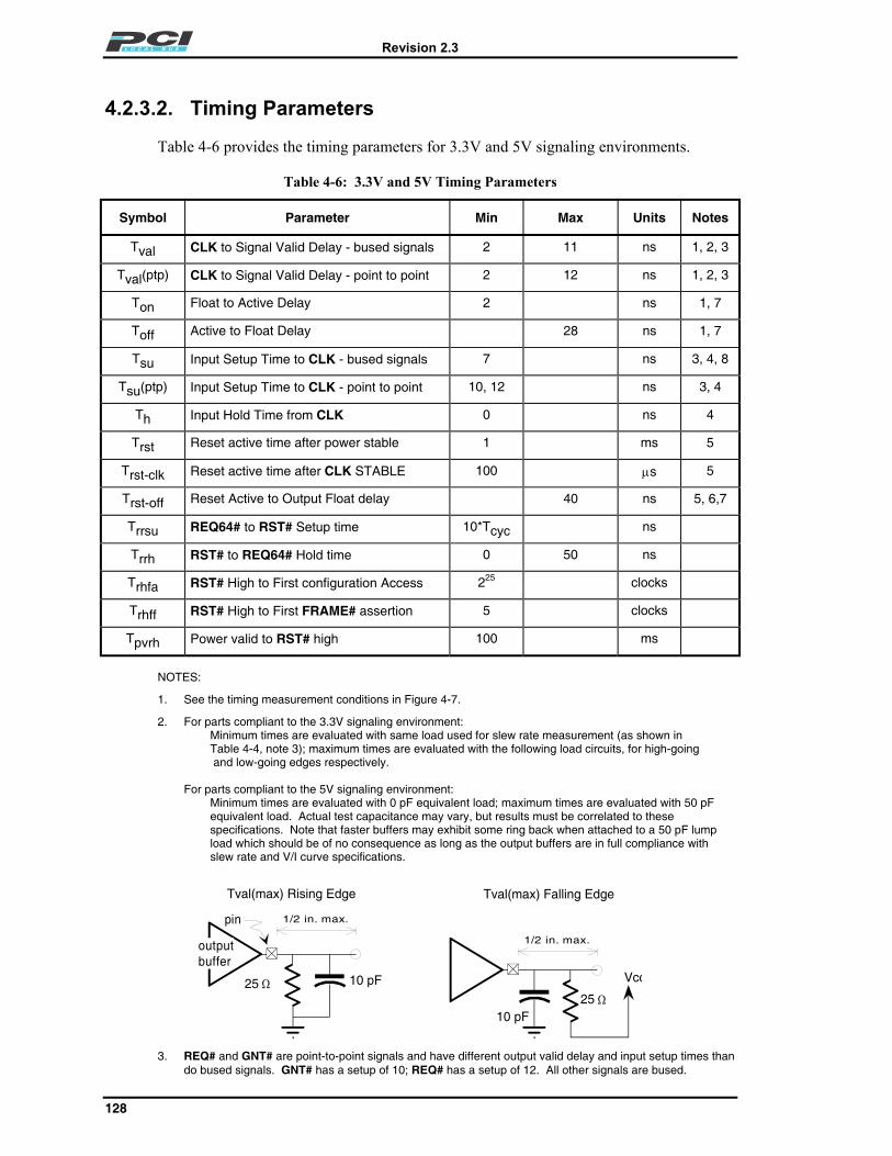
Revision 2.3
128
4.2.3.2. Timing Parameters
Table 4-6 provides the timing parameters for 3.3V and 5V signaling environments.
Table 4-6: 3.3V and 5V Timing Parameters
Symbol Parameter Min Max Units Notes
Tval CLK to Signal Valid Delay - bused signals 2 11 ns 1, 2, 3
Tval(ptp) CLK to Signal Valid Delay - point to point 2 12 ns 1, 2, 3
Ton Float to Active Delay 2 ns 1, 7
Toff Active to Float Delay 28 ns 1, 7
Tsu Input Setup Time to CLK - bused signals 7 ns 3, 4, 8
Tsu(ptp) Input Setup Time to CLK - point to point 10, 12 ns 3, 4
Th Input Hold Time from CLK 0 ns 4
Trst Reset active time after power stable 1 ms 5
Trst-clk Reset active time after CLK STABLE 100 µs 5
Trst-off Reset Active to Output Float delay 40 ns 5, 6,7
Trrsu REQ64# to RST# Setup time 10*Tcyc ns
Trrh RST# to REQ64# Hold time 0 50 ns
Trhfa RST# High to First configuration Access 225 clocks
Trhff RST# High to First FRAME# assertion 5 clocks
Tpvrh Power valid to RST# high 100 ms
NOTES:
1. See the timing measurement conditions in Figure 4-7.
2. For parts compliant to the 3.3V signaling environment:Minimum times are evaluated with same load used for slew rate measurement (as shown inTable 4-4, note 3); maximum times are evaluated with the following load circuits, for high-going and low-going edges respectively.
For parts compliant to the 5V signaling environment:Minimum times are evaluated with 0 pF equivalent load; maximum times are evaluated with 50 pFequivalent load. Actual test capacitance may vary, but results must be correlated to thesespecifications. Note that faster buffers may exhibit some ring back when attached to a 50 pF lumpload which should be of no consequence as long as the output buffers are in full compliance withslew rate and V/I curve specifications.
25 Ω10 pF
Vcc
1/2 in. max.
25 Ω 10 pF
Tval(max) Rising Edge
1/2 in. max.
outputbuffer
pin
Tval(max) Falling Edge
3. REQ# and GNT# are point-to-point signals and have different output valid delay and input setup times thando bused signals. GNT# has a setup of 10; REQ# has a setup of 12. All other signals are bused.

Revision 2.3
129
4. See the timing measurement conditions in Figure 4-8.
5. CLK is stable when it meets the requirements in Section 4.2.3.1. RST# is asserted and deassertedasynchronously with respect to CLK. Refer to Section 4.3.2. for more information.
6. All output drivers must be asynchronously floated when RST# is active. Refer to Section 3.8.1. for specialrequirements for AD[63::32], C/BE[7::4]#, and PAR64 when they are not connected (as in a 64-bit add-incard installed in a 32-bit connector).
7. For purposes of Active/Float timing measurements, the Hi-Z or “off” state is defined to be when the totalcurrent delivered through the component pin is less than or equal to the leakage current specification.
8. Setup time applies only when the device is not driving the pin. Devices cannot drive and receive signals atthe same time. Refer to Section 3.10., item 9, for additional details.
4.2.3.3. Measurement and Test Conditions
Figures 4-7 and 4-8 define the conditions under which timing measurements are made.The component test guarantees that all timings are met with minimum clock slew rate(slowest edge) and voltage swing. The design must guarantee that minimum timings arealso met with maximum clock slew rate (fastest edge) and voltage swing. In addition, thedesign must guarantee proper input operation for input voltage swings and slew rates thatexceed the specified test conditions.
CLK
OUTPUTDELAY
T_val
T_on
V_test
T_off
Tri-StateOUTPUT
V_test (5v. signaling)V_trise, V_tfall (3.3v. signaling)
V_th
V_tl
output current leakage current
Figure 4-7: Output Timing Measurement Conditions
INPUTinputsvalid
V_th
V_tl
T_hT_su
CLK
V_test
V_test
V_test V_max
V_th
V_tl
Figure 4-8: Input Timing Measurement Conditions

Revision 2.3
130
Table 4-7: Measure Condition Parameters
Symbol 3.3V Signaling 5V Signaling Units
Vth 0.6Vcc 2.4 V (Note)
Vtl 0.2Vcc 0.4 V (Note)
Vtest 0.4Vcc 1.5 V
Vtrise 0.285Vcc n/a V
Vtfall 0.615Vcc n/a V
Vmax 0.4Vcc 2.0 V (Note)
Input SignalEdge Rate
1 V/ns
NOTE:
The input test for the 3.3V environment is done with 0.1Vcc ofoverdrive; the test for the 5V environment is done with 400 mV ofoverdrive (over Vih and Vil) Timing parameters must be met with nomore overdrive than this. Vmax specifies the maximum peak-to-peakwaveform allowed for measuring input timing. Production testing mayuse different voltage values, but must correlate results back to theseparameters.
4.2.4. Indeterminate Inputs and Metastability
At times, various inputs may be indeterminate. Components must avoid logicaloperational errors and metastability by sampling inputs only on “qualified” clock edges.In general, synchronous signals are assumed to be valid and determinate only at the clockedge on which they are “qualified” (refer to Section 3.2.).
System designs must assure that floating inputs are biased away from the switchingregion in order to avoid logical, electrical, thermal, or reliability problems. In general, itis not possible to avoid situations where low slew rate signals (e.g., resistively coupledIDSEL) pass through the switching region at the time of a clock edge, but they must notbe allowed to remain at the threshold point for many clock periods. Frequently, a pre-charged bus may be assumed to retain its state while not driven for a few clock periodsduring bus turnaround.
There are specific instances when signals are known to be indeterminate. These must becarefully considered in any design.
All AD[31::00], C/BE[3::0]#, and PAR pins are indeterminate when tri-stated for busturnaround. This will sometimes last for several cycles while waiting for a device torespond at the beginning of a transaction.
The IDSEL pin is indeterminate at all times except during configuration cycles. If aresistive connection to an AD line is used, it may tend to float around the switchingregion much of the time.

Revision 2.3
131
The PME# and SERR# pins must be considered indeterminate for a number of cyclesafter they have been deasserted.
Nearly all signals will be indeterminate for as long as RST# is asserted and for a periodof time after it is released. Pins with pull-up resistors will eventually resolve high.
4.2.5. Vendor Provided Specification
The vendor of a PCI system is responsible for electrical simulation of the PCI bus andcomponents to guarantee proper operation. To help facilitate this effort, componentvendors are encouraged to make the following information available: (It is recommendedthat component vendors make this information electronically available in the IBIS modelformat.)
• Pin capacitance for all pins.
• Pin inductance for all pins.
• Output V/I curves under switching conditions. Two curves should be given for eachoutput type used: one for driving high, the other for driving low. Both should showbest-typical-worst curves. Also, "beyond-the-rail" response is critical, so the voltagerange should span -3 V to 7 V for 3.3V signaling and -5 V to 10 V for 5V signaling.
• Input V/I curves under switching conditions. A V/I curve of the input structure whenthe output is tri-stated is also important. This plot should also show best-typical-worst curves over the range of 0 to Vcc.
• Rise/fall slew rates for each output type.
• Complete absolute maximum data, including operating and non-operatingtemperature, DC maximums, etc.
In addition to this component information, connector vendors are encouraged to makeavailable accurate simulation models of PCI connectors.
4.2.6. Pinout Recommendation
This section provides a recommended pinout for PCI components. Since add-in cardstubs are so limited, layout issues are greatly minimized if the component pinout alignsexactly with the add-in card (connector) pinout. Components for use only on systemboards are encouraged also to follow this same signal ordering to allow layouts withminimum stubs. Figure 4-9 shows the recommended pinout for a typical PQFP PCIcomponent. Note that the pinout is exactly aligned with the signal order on the add-incard connector. Placement and number of power and ground pins is device-dependent.
The additional signals needed in 64-bit versions of the bus continue wrapping around thecomponent in a counter-clockwise direction in the same order they appear on the 64-bitconnector extension.

Revision 2.3
132
PCI Component
All PCI Shared SignalsBelow this Line
JTAG
RST#CLKGNTREQ
AD[31]..
AD[24]C/BE3#IDSEL
C/B
E2#
FRA
ME
#IR
DY
#TR
DY
#D
EV
SE
L#S
TOP
#LO
CK
#P
ER
R#
SE
RR
#P
AR
C/B
E1#
AD
[23]
.A
D[1
6]
AD
[15]
. .A
D[8
]
AD[0].
AD[7]C/BE0#
AD[32]..
AD[63]C/BE4#C/BE5#C/BE6#C/BE7#
REQ64#ACK64#
PCI Card Edge
PAR64
Figure 4-9: Suggested Pinout for PQFP PCI Component
Placing the IDSEL input as close as possible to AD[31::11] allows the option for a non-resistive31 connection of IDSEL to the appropriate address line with a small additionalload. Note that this pin has a lower capacitance specification that in some cases willconstrain its placement in the package.
4.3. System Board Specification
4.3.1. Clock Skew
The maximum allowable clock skew is 2 ns. This specification applies not only at asingle threshold point, but at all points on the clock edge that fall in the switching rangedefined in Table 4-8 and Figure 4-10. The maximum skew is measured between any twocomponents32 rather than between connectors. To correctly evaluate clock skew, thesystem designer must take into account clock distribution on the add-in card which isspecified in Section 4.4.
31 Non-resistive connections of IDSEL to one of the AD[xx] lines create a technical violation of the singleload per add-in card rule. PCI protocol provides for pre-driving of address lines in configuration cycles,and it is recommended that this be done in order to allow a resistive coupling of IDSEL. In absence of this,signal performance must be derated for the extra IDSEL load.
32 The system designer must address an additional source of skew. This clock skew occurs between twocomponents that have clock input trip points at opposite ends of the Vil - Vih range. In certaincircumstances, this can add to the clock skew measurement as described here. In all cases, total clock skewmust be limited to the specified number.

Revision 2.3
133
Table 4-8: Clock Skew Parameters
Symbol 3.3V Signaling 5V Signaling Units
Vtest 0.4 Vcc 1.5 V
Tskew 2 (max) 2 (max) ns
CLK(@Device #1)
CLK(@Device #2)
V_testV_ih
T_skew
T_skew
T_skew
V_testV_il
V_il
V_ih
Figure 4-10: Clock Skew Diagram
4.3.2. Reset
The assertion and deassertion of the PCI reset signal (RST#) is asynchronous withrespect to CLK. The rising (deassertion) edge of the RST# signal must be monotonic(bounce free) through the input switching range and must meet the minimum slew ratespecified in Table 4-5. The PCI specification does not preclude the implementation of asynchronous RST#, if desired. The timing parameters for reset are listed in Table 4-6with the exception of the Tfail parameter. This parameter provides for system reaction toone or both of the power rails going out of specification. If this occurs, parasitic diodepaths could short circuit active output buffers. Therefore, RST# is asserted upon powerfailure in order to float the output buffers.
The value of Tfail is the minimum of:
• 500 ns (maximum) from either power rail going out of specification (exceedingspecified tolerances by more than 500 mV)
• 100 ns (maximum) from the 5V rail falling below the 3.3V rail by more than300 mV.
The system must assert RST# during power up or in the event of a power failure. Inorder to minimize possible voltage contention between 5V and 3.3V parts, RST# must beasserted as soon as possible during the power up sequence. Figure 4-11 shows a worstcase assertion of RST# asynchronously following the "power good" signal.33 AfterRST# is asserted, PCI components must asynchronously disable (float) their outputs butare not considered reset until both Trst and Trst-clk parameters have been met. The firstrising edge of RST# after power-on for any device must be no less than Tpvrh after allthe power supply voltages are within their specified limits for that device. If RST# is
33 Component vendors should note that a fixed timing relationship between RST# and power sequencingcannot be guaranteed in all cases.

Revision 2.3
134
asserted while the power supply voltages remain within their specified limits, theminimum pulse width of RST# is Trst. Figure 4-11 shows RST# signal timing.
The system must guarantee that the bus remains in the idle state for a minimum timedelay following the deassertion of RST# to a device before the system will permit thefirst assertion of FRAME#. This time delay is included in Table 4-6 as Reset High toFirst FRAME# assertion (Trhff). If a device requires longer than the specified time(Trhff) after the deassertion of RST# before it is ready to participate in the bus signalingprotocol, then the device's state machines must remain in the reset state until all of thefollowing are simultaneously true:
• RST# is deasserted
• The device is ready to participate in the bus signaling protocol
• The bus is in the idle state
Implementation Note: Reset An example of a device that could require more than Trhff to be ready to participate inthe bus signaling protocol is a 66-MHz device that includes a Phase-Locked Loop (PLL)for distribution of the PCI clock internally to the device. The device may inhibit clocksto the PCI interface until the PLL has locked. Since the PLL could easily require morethan Trhff to lock, this could result in the clocks being enabled to the PCI interface of thisdevice in the middle of a burst transfer between two other devices. When this occurs, the66-MHz device would have to detect an idle bus condition before enabling the targetselection function.
Some PCI devices must be prepared to respond as a target Trhff time after RST#deasserts. For example, devices in the path between the CPU and the boot ROM (notexpansion ROM) must be prepared to respond as a target Trhff time after RST#deasserts.
All other devices must be prepared to respond as a target not more than Trhfa after thedeassertion of RST#. It is recommended that the system wait at least Trhfa following thedeassertion of RST# to a device before the first access to that device, unless the device isin the path between the CPU and the boot ROM or the system knows that the device isready sooner.
Software that accesses devices prior to the expiration of Trhfa must be prepared for thedevices either not to respond at all (resulting in Master-Abort) or for the devices torespond with Retry until the expiration of Trhfa. At no time can a device return invaliddata. Devices are exempt from the Maximum Retry Time specification and the targetinitial latency requirement until the expiration of Trhfa.

Revision 2.3
135
Implementation Note: Trhfa Devices are encouraged to complete their initialization and be ready to accept their firstcycle (generally a Configuration Read cycle) as soon as possible after the deassertion ofRST#. Some system implementations will access devices prior to waiting the full valueof Trhfa, if they know in advance that all devices are ready sooner. For example, asystem with no PCI slots would only need to wait for the initialization requirements ofthe embedded devices. Similarly, an intelligent add-in card that initialized its ownembedded PCI devices would only need to wait for the initialization requirements ofthose devices.
In some cases, such as intelligent add-in cards, the add-in card designer must selectdevices that initialize in less than the full value of Trhfa. For example, suppose anintelligent add-in card is not ready to respond as a target to the first Configurationtransaction from the host CPU until after the local CPU has configured the local devices.In this case, the local devices must initialize fast enough to enable the local CPU tocomplete its initialization in time for the first access from the host CPU.
PCISIGNALS
PCI_CLK
POWER
PWR_GOOD
RST#
REQ64#
Vnominal - X%
Tpvrh
tri-state
Trhff
Trhfa
Trst
Trst-clk
Trrsu
Trrh
Trst-off
Tfail
) (
) (
) (
Figure 4-11: Reset Timing 34
Refer to Section 3.8.1. for special requirements for AD[63::32], C/BE[7::4]#, andPAR64 when they are not connected (as in a 64-bit add-in card installed in a 32-bitconnector).
34 This reset timing figure optionally shows the "PWR_GOOD" signal as a pulse which is used to time theRST# pulse. In many systems, "PWR_GOOD" may be a level, in which case the RST# pulse must betimed in another way.

Revision 2.3
136
4.3.3. Pull-ups
PCI control signals always require pull-up resistors (pulled up to Vcc of the signalingenvironment) on the system board (not the add-in card) to ensure that they contain stablevalues when no agent is actively driving the bus. This includes FRAME#, TRDY#,IRDY#, DEVSEL#, STOP#, SERR#, PERR#, LOCK#, INTA#, INTB#, INTC#,INTD#, REQ64#, and ACK64#. The point-to-point and shared 32-bit signals do notrequire pull-ups; bus parking ensures their stability. Refer to Section 3.8.1. for specialrequirements for terminating AD[63::32], C/BE[7::4]#, and PAR64. Refer to Section4.3.7. for pull-up and decoupling requirements for PRSNT1# and PRSNT2#. Refer toSection 7.7.7. for pull-up and decoupling requirements for M66EN.
A system that does not support the optional SMBus interface must provide individualpull-up resistors (~5 kΩ) on the SMBCLK and SMBDAT pins for the system boardconnectors. A system that supports the SMBus interface must provide pull-up devices(passive or active) on SMBCLK and SMBDAT as defined in the SMBus 2.0Specification. Refer to Section 8 of this specification. The pull-ups must be connected tothe power source attached to the 3.3Vaux pin of the PCI connector for systems with theoptional auxiliary power supply and to +3.3V supply for systems without the optionalsupply. If boundary scan is not implemented on the system board, TMS and TDI must beindependently bused and pulled up, each with ~5 kΩ resistors, and TRST# and TCKmust be independently bused and pulled down, each with ~5 kΩ resistors. TDO must beleft open.
The formulas for minimum and maximum pull-up resistors are provided below. Rmin isprimarily driven by Iol, the DC low output current, whereas the number of loads only hasa secondary effect. On the other hand, Rmax is primarily driven by the number of loadspresent. The specification provides for a minimum R value that is calculated based on 16loads (believed to be a worst case) and a typical R value that is calculated as themaximum R value with 10 loads. The maximum R value is provided by formula onlyand will be the highest in a system with the smallest number of loads.
Rmin = [Vcc(max) − Vol] / [Iol + (16 * Iil)], where 16 = max number of loads
Rmax = [Vcc(min) – Vx] / [num_loads * Iih], where Vx = 2.7 V for 5Vsignaling and Vx = 0.7Vcc for 3.3V signaling.
Table 4-9 provides minimum and typical values for both 3.3V and 5V signalingenvironments. The typical values have been derated for 10% resistors at nominal values.
Table 4-9: Minimum and Typical Pull-up Resistor Values
Signaling Rail Rmin Rtypical Rmax
3.3V 2.42 kΩ 8.2 kΩ @ 10% see formula
5V 963 Ω 2.7 kΩ @ 10% see formula
The central resource, or any component containing an arbitration unit, may require aweak pull-up on each unconnected REQ# pin and each REQ# pin connected to a PCIslot in order to insure that these signals do not float. Values for this pull-up shall bespecified by the central resource vendor.

Revision 2.3
137
Systems utilizing PME# must provide a pull-up on that signal. The resistor value used iscalculated using the formulas above but substituting IOff for Iih.
4.3.4. Power
4.3.4.1. Power Requirements
All PCI connectors require four power rails: +5V, +3.3V, +12V, and -12V. Systems thatprovide PCI connectors are required to provide all four rails in every system with thecurrent budget specified in Table 4-10. Systems may optionally supply 3.3Vaux power,as specified in the PCI Bus Power Management Interface Specification. Systems that donot support PCI bus power management must treat the 3.3Vaux pin as reserved.
Current requirements per connector for the two 12V rails are provided in Table 4-10.There are no specific system requirements for current per connector on the 3.3V and 5Vrails; this is system dependent. Note that Section 4.4.2.2. requires that an add-in cardmust limit its total power consumption to 25 watts (from all power rails). The systemprovides a total power budget for add-in cards that can be distributed between connectorsin an arbitrary way. The PRSNTn# pins on the connector allow the system to optionallyassess the power demand of each add-in card and determine if the installed configurationwill run within the total power budget. Refer to Section 4.4.1. for further details.
Table 4-10 specifies the tolerances of supply rails. Note that these tolerances are to beguaranteed at the components not the supply.
Table 4-10: Power Supply Rail Tolerances
Power Rail Add-in Cards (Short and Long)
3.3 V ±0.3 V 7.6 A max. (system dependent)
5 V ± 5 % 5 A max. (system dependent)
12 V ±5% 500 mA max.
-12 V ±10% 100 mA max.
4.3.4.2. Sequencing
There is no specified sequence in which the four power rails are activated or deactivated.They may come up and go down in any order. The system must assert RST# both atpower up and whenever either the 3.3V or 5V rails go out of specification (perSection 4.3.2.). During reset, all PCI signals are driven to a "safe" state, as described inSection 4.3.2.

Revision 2.3
138
4.3.4.3. Decoupling
All power planes must be decoupled to ground to provide:
• reasonable management of the switching currents (d I/d t) to which the plane and itssupply path are subjected
• an AC return path in a manner consistent with high-speed signaling techniques
This is platform dependent and not detailed in the specification.
4.3.5. System Timing Budget
When computing a total PCI load model, careful attention must be paid to maximumtrace length and loading of add-in cards, as specified in Section 4.4.3. Also, themaximum pin capacitance of 10 pF must be assumed for add-in cards, whereas the actualpin capacitance may be used for system board devices.
The total clock period can be divided into four segments. Valid output delay (Tval) andinput setup time (Tsu) are specified by the component specification. Total clock skew(Tskew) and maximum bus propagation time (Tprop) are system parameters. Tprop isspecified as 10 ns but may be increased to 11 ns by lowering clock skew; that is, Tpropplus Tskew together may not exceed 12 ns; however, under no circumstance may Tskewexceed 2 ns. Furthermore, by using clock rates slower than 33 MHz, some systems maybuild larger PCI topologies having Tprop values larger than those specified here. Sincecomponent times (Tval and Tsu) and clock skew are fixed, any increase in clock cycletime allows an equivalent increase in Tprop. For example, at 25 MHz (40 ns clockperiod), Tprop may be increased to 20 ns. Note that this tradeoff affects system boardsonly; all add-in card designs must assume 33 MHz operation.
Tprop is measured as shown in Figure 4-12 and Figure 4-13. It begins at the time thesignal at the output buffer would have crossed the threshold point of Vtrise or Vtfall for3.3V signaling (Vtest in Figure 4-13 for 5V signaling) had the output been driving thespecified Tval load (50 pF lump load for 5V signaling). The end of Tprop for anyparticular input is determined by one of the following two measurement methods. Themethod that produces the longer value for Tprop must be used.
Method 1: The end of Tprop is the time when the signal at the input crosses Vtest for thelast time in Figure 4-12 a, d. (See Figure 4-13 a, d for 5V signaling.)
Method 2: Construct a line with a slope equal to the Input Signal Edge Rate shown inTable 4-7 and crossing through the point where the signal at the input crossesVih (high going) or Vil (low going) for the last time. The end of Tprop is thetime when the constructed line crosses Vtest in Figure 4-12 b, c, e, f. (SeeFigure 4-13 b, c, e, f for 5V signaling.)

Revision 2.3
139
Implementation Note: Determining the End of TpropThe end of Tprop is always determined by the calculation method that produces thelonger value of Tprop. The shape of the waveform at the input buffer will determinewhich measurement method will produce the longer value.
When the signal rises or falls from Vtest to the last crossing of Vih (high going) or Vil(low going) faster than the Input Signal Edge Rate shown in Table 4-7, Method 1 willproduce the longer value as shown in Figure 4-12 a, d for 3.3V signaling. (See Figure 4-13 a, d for 5V signaling.)
When the signal rises or falls from Vtest to the last crossing of Vih (high going) or Vil(low going) slower than the Input Signal Edge Rate, Method 2 will produce the longervalue. In other words, if the signal plateaus or rises (high going) or falls (low going)slowly after crossing Vtest, or rings back across Vih (high going) or Vil (low going)significantly after crossing Vtest, Method 2 will produce the longer value as shown inFigure 4-12 b, c, e, f for 3.3V signaling. (See Figure 4-13 b, c, e, f for 5V signaling.)
Refer to Table 4-1, Table 4-3, and Table 4-7 for the values of parameters in Figure 4-12and Figure 4-13 in 33-MHz mode. Refer to Chapter 7 for a description of 66-MHzoperation.
For a given driver location, the worst case that must be considered when determining thevalue of Tprop is when the signal settles at all other devices on the bus. The value ofTprop is not affected by the time the signal settles at the driver output, since devices arenot permitted to drive and receive a signal at the same time. Refer to Section 3.10, item 9for additional details.
In many system layouts, correct PCI signal propagation relies on diodes embedded in PCIcomponents to limit reflections and successfully meet Tprop. In configurations whereunterminated trace ends propagate a significant distance from a PCI component (e.g., asection of unpopulated add-in card connectors), it may be necessary to add active (e.g.,diode) termination at the unloaded end of the bus in order to insure adequate signalquality. Note that since the signaling protocol depends on the initial reflection, passivetermination does not work.

Revision 2.3
140
(b)(a)
0.7Vcc
0.6Vcc
0.5Vcc
0.4Vcc
0.3Vcc
0.2Vcc
0.1Vcc
0
testV
triseV
ihV
propT
propT
propTpropT
propT
propT
testV
triseV
ihV
thV
testV
ilV
tlV
tfallV
DrivingTest Load
DrivingTest Load
DrivingBus
Input SignalSlew RateDriving Bus
DrivingTest Load
DrivingBus
DrivingTest Load
Input SignalSlew Rate
Driving Bus
testV
ilV
tlV
tfallV
DrivingTest Load
Driving Bus
DrivingTest Load
Driving Bus
Input SignalSlew Rate
(f)(e)
0.9Vcc
0.8Vcc
0.7Vcc
0.6Vcc
0.5Vcc
0.4Vcc
0.3Vcc
0.2Vcc
0.1Vcc
0
(d)(c)
0.9Vcc
0.8Vcc
0.7Vcc
0.6Vcc
0.5Vcc
0.4Vcc
0.3Vcc
0.2Vcc
0.1Vcc
0
Input SignalSlew Rate
0.7Vcc
0.6Vcc
0.5Vcc
0.4Vcc
0.3Vcc
0.2Vcc
0.1Vcc
0
0.9Vcc
0.8Vcc
0.7Vcc
0.6Vcc
0.5Vcc
0.4Vcc
0.3Vcc
0.2Vcc
0.1Vcc
0
0.9Vcc
0.8Vcc
0.7Vcc
0.6Vcc
0.5Vcc
0.4Vcc
0.3Vcc
0.2Vcc
0.1Vcc
0
testV
triseV
ihV
thV
testV
ilV
tlV
tfallV
Figure 4-12: Measurement of Tprop, 3.3 Volt Signaling

Revision 2.3
141
DrivingBus
DrivingTest Load
2.0V
1.0V
thV
ihV
testVDrivingBus
DrivingTest Load
thV
ihV
testV
DrivingBus
DrivingTest Load
2.0V
1.0V
thV
ihV
testV
Driving Bus
Driving Test Load
tlV
ilV
testV
DrivingBus
Tprop
2.0V
1.0V
tlV
ilV
testV
DrivingTest Load
ilV
tlV
testV
InputSignalEdgeRate
Input SignalEdge Rate
Driving Test Load
Input SignalEdge Rate
Input SignalEdge Rate
Driving Bus
(a) (b)
(c) (d)
(e) (f)
2.0V
1.0V
2.0V
1.0V
2.0V
1.0V
Tprop
Tprop Tprop
Tprop
Tprop
Figure 4-13: Measurement of Tprop, 5 Volt Signaling

Revision 2.3
142
4.3.6. Physical Requirements
4.3.6.1. Routing and Layout Recommendations for Four-LayerSystem Boards
The power pins have been arranged on the connector to facilitate layouts on four layersystem boards. A "split power plane" is permitted - creating a 3.3V island in the 5Vplane, which connects all the 3.3V PCI connector pins and may optionally have a powerdistribution "finger" reaching to the power supply connector. Although this is a standardtechnique, routing high speed signals directly over this plane split can cause signalintegrity problems. The split in the plane disrupts the AC return path for the signalcreating an impedance discontinuity.
A recommended solution is to arrange the signal level layouts so that no high speedsignal (e.g., 33 MHz) is referenced to both planes. Signal traces should either remainentirely over the 3.3V plane or entirely over the 5V plane. Signals that must cross fromone domain to the other should be routed on the opposite side of the system board so thatthey are referenced to the ground plane which is not split. If this is not possible, andsignals must be routed over the plane split, the two planes should be capacitively tiedtogether (5V plane decoupled directly to 3.3V plane) with 0.01 µF high-speed capacitorsfor each four signals crossing the split and the capacitor should be placed not more than0.25 inches from the point the signals cross the split.
4.3.6.2. System Board Impedance
There is no bare board impedance specification for system boards. The system designerhas two primary constraints in which to work:
• The length and signal velocity must allow a full round trip time on the bus within thespecified propagation delay of 10 ns. (Refer to Section 4.3.5.)
• The loaded impedance seen at any drive point on the network must be such that a PCIoutput device (as specified by its V/I curve) can meet input device specifications witha single reflection of the signal. This includes loads presented by add-in cards.
Operating frequency may be traded off for additional round trips on the bus to buildconfigurations that might not comply with the two constraints mentioned above. Thisoption is neither recommended nor specifically precluded.
Revision 2.3
143
4.3.7. Connector Pin Assignments
The PCI connector contains all the signals defined for PCI components, plus two pinsthat are related to the connector only. These pins, PRSNT1# and PRSNT2#, aredescribed in Section 4.4.1. System boards must decouple both of these pins individuallyto ground with 0.01 µF high-speed capacitors, because one or both of the pins alsoprovide an AC return path. These pins may not be bused or otherwise connected to eachother on the system board. Further use of these pins on the system board is optional. Ifthe system board design accesses these pins to obtain add-in card information, each pinmust have an appropriate pull-up resistor (of approximately 5 kΩ) on the system board.The connector pin assignments are shown in Table 4-11. Pins labeled “Reserved” mustbe left unconnected on all connectors.
Pin 38B is a special pin that has logical significance in PCI-X capable slots. In PCI-Xslots, pin 38B must be handled as indicated in the PCIXCAP Connection section of thePCI-X Addendum to the PCI Local Bus Specification. For all other PCI connectors, thispin must be treated in all respects as a standard ground pin; i.e., the connector pin must beconnected to the ground plane.
Pin 49B is a special purpose pin that has logical significance in 66-MHz-capable slots,and, in such slots, it must be separately bused, pulled up, and decoupled as described inSection 7.7.7. For all other PCI connectors, this pin must be treated in all respects as astandard ground pin; i.e., the connector pin must be connected to the ground plane.

Revision 2.3
144
Table 4-11: PCI Connector Pinout
3.3V System Environment 5V System Environment
Pin Side B Side A Side B Side A Comments
1 -12V TRST# -12V TRST# 32-bit connector start
2 TCK +12V TCK +12V3 Ground TMS Ground TMS4 TDO TDI TDO TDI5 +5V +5V +5V +5V6 +5V INTA# +5V INTA#7 INTB# INTC# INTB# INTC#8 INTD# +5V INTD# +5V9 PRSNT1# Reserved PRSNT1# Reserved10 Reserved +3.3V (I/O) Reserved +5V (I/O)
11 PRSNT2# Reserved PRSNT2# Reserved12 CONNECTOR KEY Ground Ground 3.3 volt key
13 CONNECTOR KEY Ground Ground 3.3 volt key
14 Reserved 3.3Vaux Reserved 3.3Vaux15 Ground RST# Ground RST#16 CLK +3.3V (I/O) CLK +5V (I/O)
17 Ground GNT# Ground GNT#18 REQ# Ground REQ# Ground19 +3.3V (I/O) PME# +5V (I/O) PME#20 AD[31] AD[30] AD[31] AD[30]21 AD[29] +3.3V AD[29] +3.3V22 Ground AD[28] Ground AD[28]23 AD[27] AD[26] AD[27] AD[26]24 AD[25] Ground AD[25] Ground25 +3.3V AD[24] +3.3V AD[24]26 C/BE[3]# IDSEL C/BE[3]# IDSEL27 AD[23] +3.3V AD[23] +3.3V28 Ground AD[22] Ground AD[22]29 AD[21] AD[20] AD[21] AD[20]30 AD[19] Ground AD[19] Ground31 +3.3V AD[18] +3.3V AD[18]32 AD[17] AD[16] AD[17] AD[16]33 C/BE[2]# +3.3V C/BE[2]# +3.3V34 Ground FRAME# Ground FRAME#35 IRDY# Ground IRDY# Ground36 +3.3V TRDY# +3.3V TRDY#37 DEVSEL# Ground DEVSEL# Ground38 PCIXCAP STOP# Ground STOP#39 LOCK# +3.3V LOCK# +3.3V40 PERR# SMBCLK PERR# SMBCLK41 +3.3V SMBDAT +3.3V SMBDAT42 SERR# Ground SERR# Ground

Revision 2.3
145
Table 4-11: PCI Connector Pinout (continued)
3.3V System Environment 5V System Environment
Pin Side B Side A Side B Side A Comments
43 +3.3V PAR +3.3V PAR44 C/BE[1]# AD[15] C/BE[1]# AD[15]45 AD[14] +3.3V AD[14] +3.3V46 Ground AD[13] Ground AD[13]47 AD[12] AD[11] AD[12] AD[11]48 AD[10] Ground AD[10] Ground49 M66EN AD[09] Ground AD[09] 66 MHz / gnd
50 Ground Ground CONNECTOR KEY 5 volt key
51 Ground Ground CONNECTOR KEY 5 volt key
52 AD[08] C/BE[0]# AD[08] C/BE[0]#53 AD[07] +3.3V AD[07] +3.3V54 +3.3V AD[06] +3.3V AD[06]55 AD[05] AD[04] AD[05] AD[04]56 AD[03] Ground AD[03] Ground57 Ground AD[02] Ground AD[02]58 AD[01] AD[00] AD[01] AD[00]59 +3.3V (I/O) +3.3V (I/O) +5V (I/O) +5V (I/O)
60 ACK64# REQ64# ACK64# REQ64#61 +5V +5V +5V +5V62 +5V +5V +5V +5V 32-bit connector end
CONNECTOR KEY CONNECTOR KEY 64-bit spacerCONNECTOR KEY CONNECTOR KEY 64-bit spacer
63 Reserved Ground Reserved Ground 64-bit connector start
64 Ground C/BE[7]# Ground C/BE[7]#65 C/BE[6]# C/BE[5]# C/BE[6]# C/BE[5]#66 C/BE[4]# +3.3V (I/O) C/BE[4]# +5V (I/O)
67 Ground PAR64 Ground PAR6468 AD[63] AD[62] AD[63] AD[62]69 AD[61] Ground AD[61] Ground70 +3.3V (I/O) AD[60] +5V (I/O) AD[60]71 AD[59] AD[58] AD[59] AD[58]72 AD[57] Ground AD[57] Ground73 Ground AD[56] Ground AD[56]74 AD[55] AD[54] AD[55] AD[54]75 AD[53] +3.3V (I/O) AD[53] +5V (I/O)
76 Ground AD[52] Ground AD[52]77 AD[51] AD[50] AD[51] AD[50]78 AD[49] Ground AD[49] Ground79 +3.3V (I/O) AD[48] +5V (I/O) AD[48]80 AD[47] AD[46] AD[47] AD[46]81 AD[45] Ground AD[45] Ground82 Ground AD[44] Ground AD[44]

Revision 2.3
146
Table 4-11: PCI Connector Pinout (continued)
3.3V System Environment 5V System Environment
Pin Side B Side A Side B Side A Comments
83 AD[43] AD[42] AD[43] AD[42]84 AD[41] +3.3V (I/O) AD[41] +5V (I/O)
85 Ground AD[40] Ground AD[40]86 AD[39] AD[38] AD[39] AD[38]87 AD[37] Ground AD[37] Ground88 +3.3V (I/O) AD[36] +5V (I/O) AD[36]89 AD[35] AD[34] AD[35] AD[34]90 AD[33] Ground AD[33] Ground91 Ground AD[32] Ground AD[32]92 Reserved Reserved Reserved Reserved93 Reserved Ground Reserved Ground94 Ground Reserved Ground Reserved 64-bit connector end
Pins labeled "+3.3V (I/O)" and "+5V (I/O)" are special power pins for defining and drivingthe PCI signaling rail on the Universal add-in card. On the system board, these pins areconnected to the main +3.3V or +5V plane, respectively.
Refer to Section 3.8.1. for special requirements for the connection of REQ64# on 32-bit-only slot connectors.
Revision 2.3
147
4.4. Add-in Card Specification
4.4.1. Add-in Card Pin Assignment
The PCI connector contains all the signals defined for PCI components, plus two pinsthat are related to the connector only. These are PRSNT1# and PRSNT2#. They areused for two purposes: indicating that an add-in card is physically present in the slot andproviding information about the total power requirements of the add-in card. Table 4-12defines the required setting of the PRSNT# pins for add-in cards.
Table 4-12: Present Signal Definitions
PRSNT1# PRSNT2# Add-in Card Configuration
Open Open No add-in card present
Ground Open Add-in card present, 25 W maximum
Open Ground Add-in card present, 15 W maximum
Ground Ground Add-in card present, 7.5 W maximum
In providing a power level indication, the add-in card must indicate total maximumpower consumption for the add-in card, including all supply voltages. The add-in cardsmay optionally draw all this power from either the 3.3V or 5V power rail. Furthermore,if the add-in card is configurable (e.g., sockets for memory expansion, etc.), the pinstrapping must indicate the total power consumed by a fully configured add-in card,which may be more than that consumed in its shipping configuration.
Add-in cards that do not implement JTAG Boundary Scan are required to connect TDIand TDO (pins 4A and 4B) so the scan chain is not broken.
Pin 38B is a special pin that has logical significance in PCI-X capable add-in cards. InPCI-X slots, pin 38B must be handled as indicated in the PCIXCAP Connection sectionof the PCI-X Addendum to the PCI Local Bus Specification. For all other PCI add-incards, this pin must be treated in all respects as a standard ground pin; i.e., the edge fingermust be plated and connected to the ground plane of the add-in card.
Pin 49B is a special purpose pin that has logical significance in 66-MHz-capable add-incards, and, in such add-in cards, it must be connected and decoupled as described inSection 7.8. For all other add-in cards, this pin must be treated in all respects as astandard ground pin; i.e., the edge finger must be plated and connected to the groundplane of the add-in card.

Revision 2.3
148
Table 4-13: PCI Add-in Card Pinout
Universal Add-in Card 3.3V Add-in Card
Pin Side B Side A Side B Side A Comments
1 -12V TRST# -12V TRST# 32-bit start
2 TCK +12V TCK +12V3 Ground TMS Ground TMS4 TDO TDI TDO TDI5 +5V +5V +5V +5V6 +5V INTA# +5V INTA#7 INTB# INTC# INTB# INTC#8 INTD# +5V INTD# +5V9 PRSNT1# Reserved PRSNT1# Reserved10 Reserved +VI/O Reserved +3.3V11 PRSNT2# Reserved PRSNT2# Reserved12 KEYWAY KEYWAY 3.3V key
13 KEYWAY KEYWAY 3.3V key
14 Reserved 3.3Vaux Reserved 3.3Vaux15 Ground RST# Ground RST#16 CLK +VI/O CLK +3.3V17 Ground GNT# Ground GNT#18 REQ# Ground REQ# Ground19 +VI/O PME# +3.3V PME#20 AD[31] AD[30] AD[31] AD[30]21 AD[29] +3.3V AD[29] +3.3V22 Ground AD[28] Ground AD[28]23 AD[27] AD[26] AD[27] AD[26]24 AD[25] Ground AD[25] Ground25 +3.3V AD[24] +3.3V AD[24]26 C/BE[3]# IDSEL C/BE[3]# IDSEL27 AD[23] +3.3V AD[23] +3.3V28 Ground AD[22] Ground AD[22]29 AD[21] AD[20] AD[21] AD[20]30 AD[19] Ground AD[19] Ground31 +3.3V AD[18] +3.3V AD[18]32 AD[17] AD[16] AD[17] AD[16]33 C/BE[2]# +3.3V C/BE[2]# +3.3V34 Ground FRAME# Ground FRAME#35 IRDY# Ground IRDY# Ground36 +3.3V TRDY# +3.3V TRDY#37 DEVSEL# Ground DEVSEL# Ground38 PCIXCAP STOP# PCIXCAP STOP#39 LOCK# +3.3V LOCK# +3.3V40 PERR# SMBCLK PERR# SMBCLK41 +3.3V SMBDAT +3.3V SMBDAT42 SERR# Ground SERR# Ground

Revision 2.3
149
Table 4-13: PCI Add-in Card Pinout (continued)
Universal Add-in Card 3.3V Add-in Card
Pin Side B Side A Side B Side A Comments
43 +3.3V PAR +3.3V PAR44 C/BE[1]# AD[15] C/BE[1]# AD[15]45 AD[14] +3.3V AD[14] +3.3V46 Ground AD[13] Ground AD[13]47 AD[12] AD[11] AD[12] AD[11]48 AD[10] Ground AD[10] Ground49 M66EN AD[09] M66EN AD[09] 66 MHz /gnd
50 KEYWAY Ground Ground 5V key
51 KEYWAY Ground Ground 5V key
52 AD[08] C/BE[0]# AD[08] C/BE[0]#53 AD[07] +3.3V AD[07] +3.3V54 +3.3V AD[06] +3.3V AD[06]55 AD[05] AD[04] AD[05] AD[04]56 AD[03] Ground AD[03] Ground57 Ground AD[02] Ground AD[02]58 AD[01] AD[00] AD[01] AD[00]59 +VI/O +VI/O +3.3V +3.3V60 ACK64# REQ64# ACK64# REQ64#61 +5V +5V +5V +5V62 +5V +5V +5V +5V 32-bit end
KEYWAY KEYWAY 64-bit spacerKEYWAY KEYWAY 64-bit spacer
63 Reserved Ground Reserved Ground 64-bit start
64 Ground C/BE[7]# Ground C/BE[7]#65 C/BE[6]# C/BE[5]# C/BE[6]# C/BE[5]#66 C/BE[4]# +VI/O C/BE[4]# +3.3V67 Ground PAR64 Ground PAR6468 AD[63] AD[62] AD[63] AD[62]69 AD[61] Ground AD[61] Ground70 +VI/O AD[60] +3.3V AD[60]71 AD[59] AD[58] AD[59] AD[58]72 AD[57] Ground AD[57] Ground73 Ground AD[56] Ground AD[56]74 AD[55] AD[54] AD[55] AD[54]75 AD[53] +VI/O AD[53] +3.3V76 Ground AD[52] Ground AD[52]77 AD[51] AD[50] AD[51] AD[50]78 AD[49] Ground AD[49] Ground79 +VI/O AD[48] +3.3V AD[48]80 AD[47] AD[46] AD[47] AD[46]81 AD[45] Ground AD[45] Ground82 Ground AD[44] Ground AD[44]

Revision 2.3
150
Table 4-13: PCI Add-in Card Pinout (continued)
Universal Add-in Card 3.3V Add-in Card
Pin Side B Side A Side B Side A Comments
83 AD[43] AD[42] AD[43] AD[42]84 AD[41] +VI/O AD[41] +3.3V85 Ground AD[40] Ground AD[40]86 AD[39] AD[38] AD[39] AD[38]87 AD[37] Ground AD[37] Ground88 +VI/O AD[36] +3.3V AD[36]89 AD[35] AD[34] AD[35] AD[34]90 AD[33] Ground AD[33] Ground91 Ground AD[32] Ground AD[32]92 Reserved Reserved Reserved Reserved93 Reserved Ground Reserved Ground94 Ground Reserved Ground Reserved 64-bit end
Table 4-14: Pin Summary - 32-bit Add-in Card
Pin Type Universal Add-in Card 3.3V Add-in Card
Ground 18 (Note) 22 (Note)+5 V 8 8
+3.3 V 12 17I/O pwr 5 0
Reserv'd 4 4
NOTE:
If the PCIXCAP and M66EN pins are implemented, the numberof ground pins for a Universal add-in card is 16 and the numberof ground pins for a 3.3V add-in card is 20.
Table 4-15: Pin Summary - 64-bit Add-in Card (incremental pins)
Pin Type Universal Add-in Card 3.3V Add-in Card
Ground 16 16+5 V 0 0
+3.3 V 0 6I/O pwr 6 0
Reserv'd 5 5

Revision 2.3
151
Pins labeled "+VI/O" are special power pins for defining and driving the PCI signalingrail on the Universal add-in card. On this add-in card, the PCI component's I/O buffersmust be powered from these special power pins only35—not from the other +3.3V or +5Vpower pins.
4.4.2. Power Requirements
4.4.2.1. Decoupling
Under typical conditions, the Vcc plane to ground plane capacitance will provideadequate decoupling for the Vcc connector pins. The maximum trace length from aconnector pad to the Vcc/GND plane via shall be 0.25 inches (assumes a 20 mil tracewidth).
However, on the Universal add-in card, it is likely that the I/O buffer power rail will nothave adequate capacitance to the ground plane to provide the necessary decoupling. Pinslabeled "+VI/O" should be decoupled to ground with an average of 0.047 µF per pin.
Additionally, all +3.3V pins and any unused +5V and VI/O pins on the PCI edgeconnector provide an AC return path and must have plated edge fingers and be coupled tothe ground plane on the add-in card as described below to ensure they continue tofunction as efficient AC reference points:
1. The decoupling must average at least 0.01 µF (high-speed) per Vcc pin.
2. The trace length from pin pad to capacitor pad shall be no greater than 0.25 inchesusing a trace width of at least 0.02 inches.
3. There is no limit to the number of pins that can share the same capacitor providedthat requirements 1 and 2 are met.
All edge fingers must be plated and all ground edge fingers must be connected to theground plane on the add-in card.
4.4.2.2. Power Consumption
The maximum power allowed for any add-in card is 25 watts, and represents the totalpower drawn from all power rails provided at the connector (+3.3V, +5V, +VI/O, +12V,-12V, +3.3Vaux). The add-in card may optionally draw all this power from either the+3.3V or +5V rail.
It is anticipated that many systems will not provide a full 25 watts per connector for eachpower rail, because most add-in cards will typically draw much less than this amount.For this reason, it is recommended that add-in cards that consume more than 10 watts
35 When “5V tolerant parts” are used on the Universal add-in card, its I/O buffers may optionally beconnected to the 3.3V rail rather than the "I/O" designated power pins; but high clamp diodes may still beconnected to the "I/O" designated power pins. (Refer to the last paragraph of Section 4.2.1.2. - "Clampingdirectly to the 3.3V rail with a simple diode must never be used in the 5V signaling environment.") Sincethe effective operation of these high clamp diodes may be critical to both signal quality and devicereliability, the designer must provide enough "I/O" designated power pins on a component to handle thecurrent spikes associated with the 5V maximum AC waveforms (Section 4.2.1.3.).

Revision 2.3
152
power up in and reset to a reduced-power state that consumes 10 watts or less. While inthis state, the add-in card must provide full access to its PCI Configuration Space andmust perform required bootstrap functions, such as basic text mode on a video add-incard. All other add-in card functions can be suspended if necessary. This power savingstate can be achieved in a variety of ways. For example:
• Clock rates on the add-in card can be reduced, which reduces performance but doesnot limit functionality.
• Power planes to non-critical parts could be shut off with a FET, which could limitfunctional capability.
After the driver for the add-in card has been initialized, it may place the add-in card into afully powered, full function/performance state using a device dependent mechanism ofchoice (probably register based). In advanced power managed systems, the device drivermay be required to report the target power consumption before fully enabling the add-incard in order to allow the system to determine if it has a sufficient power budget for alladd-in cards in the current configuration.
Add-in cards must never source any power back to the system board, except in the casewhere an add-in card has been specifically designed to provide a given system’s power.In some cases, add-in cards capable of 3.3V PCI signaling have multiple mechanisms thatindirectly source power back to the system and will violate this requirement if notproperly controlled. For example, add-in cards containing components with bus clampsto the 3.3V rail may create a “charge pump” which directs excess bus switching energyback into the system board. Alternately, I/O output buffers operating on the 3.3V rail,but used in a 5V signaling environment, may bleed the excess charge off the bus and intothe 3.3V power net when they drive the bus “high” after it was previously driven to the5V rail. Unintentional power sourcing by any such mechanism must be managed byproper decoupling and sufficient local load on the supply (bleed resistor or otherwise) todissipate any power “generated” on the add-in card. This requirement does not apply tonoise generated on the power rail as long as the net DC current accumulated over any twoclock periods is zero.
4.4.3. Physical Requirements
4.4.3.1. Trace Length Limits
Trace lengths from the top of the add-in card’s edge connector to the PCI device are asfollows:
• The maximum trace lengths for all 32-bit interface signals are limited to 1.5 inchesfor 32-bit and 64-bit add-in cards. This includes all signal groups (refer to Section2.2.) except those listed as “System Pins,” “Interrupt Pins,” “SMBus,” and “JTAGPins.”
• The trace lengths of the additional signals used in the 64-bit extension are limited to2 inches on all 64-bit add-in cards.
• The trace length for the PCI CLK signal is 2.5 inches ± 0.1 inches for 32-bit and64-bit add-in cards and must be routed to only one load.

Revision 2.3
153
4.4.3.2. Routing Recommendations for Four-Layer Add-in Cards
The power pins have been arranged on the connector to facilitate layouts on four layeradd-in cards. A "split power plane" is permitted, as described in Section 4.3.6.1.Although this is a standard technique, routing high speed signals directly over this planesplit can cause signal integrity problems. The split in the plane disrupts the AC returnpath for the signal creating an impedance discontinuity.
A recommended solution is to arrange the signal level layouts so that no high speedsignal (e.g., 33 MHz) is referenced to both planes. Signal traces should either remainentirely over the 3.3V plane or entirely over the 5V plane. Signals that must cross fromone domain to the other should be routed on the opposite side of the add-in card so thatthey are referenced to the ground plane which is not split. If this is not possible, andsignals must be routed over the plane split, the two planes should be capacitively tiedtogether (5V plane decoupled directly to 3.3V plane) with 0.01 µF high-speed capacitorsfor each four signals crossing the split and the capacitor should be placed not more than0.25 inches from the point the signals cross the split.
4.4.3.3. Impedance
The unloaded characteristic impedance (Z0) of the shared PCI signal traces on the add-incard shall be controlled to be in the 60 Ω - 100 Ω range if the device input capacitance(Cin) exceeds 8 pF. If Cin is 8 pF or less, the range for Z0 is 51 Ω - 100 Ω. The tracevelocity must be between 150 ps/inch and 190 ps/inch.
4.4.3.4. Signal Loading
Shared PCI signals must be limited to one load on the add-in card. Violation of add-incard trace length or loading limits will compromise system signal integrity. It isspecifically a violation of this specification for add-in cards to:
• Attach an expansion ROM directly (or via bus transceivers) on any PCI pins.
• Attach two or more PCI devices on an add-in card, unless they are placed behind aPCI-to-PCI bridge.
• Attach any logic (other than a single PCI device) that "snoops" PCI pins.
• Use PCI component sets that place more than one load on each PCI pin; e.g., separateaddress and data path components.
• Use a PCI component that has more than 10 pF capacitance per pin.
• Attach any pull-up resistors or other discrete devices to the PCI signals, unless theyare placed behind a PCI-to-PCI bridge.
The SMBus signal group is exempt from this requirement. Refer to Section 8.2.5 forSMBus signal loading requirements.

Revision 2.3
154

Revision 2.3
155
Chapter 5Mechanical Specification
5.1. OverviewThe PCI add-in card is based on a raw add-in card design (see Figures 5-1 to 5-4) that iseasily implemented in existing chassis designs from multiple manufacturers. PCI add-incards have three basic form factors: standard length, short length, and low profile. Thestandard length card provides 49 square inches of real estate. The fixed and variableheight short length cards were chosen for panel optimization to provide the lowest costfor a function. The fixed and variable height short cards also provide the lowest cost toimplement in a system, the lowest energy consumption, and allow the design of smallersystems. The interconnect for the PCI add-in card has been defined for both the 32-bitand 64-bit interfaces.
PCI add-in cards and connectors are keyed to manage the 5V to 3.3V transition. Thebasic 32-bit connector contains 120 pins. The logical numbering of pins shows 124 pinidentification numbers, but four pins are not present and are replaced by the keyinglocation. In one orientation, the connector on the system board is keyed to accept 3.3Vsystem signaling environment add-in cards; turned 180 degrees, the key is located toaccept 5V system signaling add-in cards. Universal add-in cards, add-in cards built towork in both 3.3V and 5V system signaling environments, have two key slots so that theycan plug into either connector. A 64-bit extension, built onto the same connectormolding, extends the total number of pins to 184. The 32-bit connector subset defines thesystem signaling environment. 32-bit add-in cards and 64-bit add-in cards are inter-operable within the system's signaling voltage classes defined by the keying in the 32-bitconnector subset. A 32-bit add-in card identifies itself for 32-bit transfers on the 64-bitconnector. A 64-bit add-in card in a 32-bit connector must configure for 32-bit transfers.
Maximum add-in card power dissipation is encoded on the PRSNT1# and PRSNT2#pins of the add-in card. This hard encoding can be read by system software uponinitialization. The system's software can then make a determination whether adequatecooling and supply current is available in that system for reliable operation at start-up andinitialization time. Supported power levels and their encoding are defined in Chapter 4.
The PCI add-in card includes a mounting bracket for add-in card location and retention.The backplate is the interface between the add-in card and the system that provides forcable escapement. The retainer fastens to the front edge of the PCI add-in card to providesupport via a standard PCI add-in card guide.
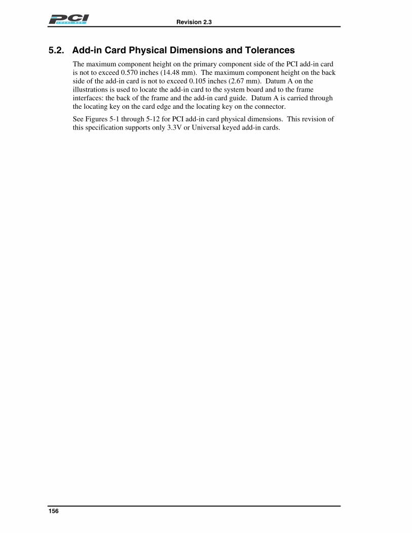
Revision 2.3
156
5.2. Add-in Card Physical Dimensions and TolerancesThe maximum component height on the primary component side of the PCI add-in cardis not to exceed 0.570 inches (14.48 mm). The maximum component height on the backside of the add-in card is not to exceed 0.105 inches (2.67 mm). Datum A on theillustrations is used to locate the add-in card to the system board and to the frameinterfaces: the back of the frame and the add-in card guide. Datum A is carried throughthe locating key on the card edge and the locating key on the connector.
See Figures 5-1 through 5-12 for PCI add-in card physical dimensions. This revision ofthis specification supports only 3.3V or Universal keyed add-in cards.

Revision 2.3
157
(3X)
10.
16[.4
00]
10.1
6[.4
00]
1[.0
39]
(2X)
250
.71
[9.8
70]
TOLE
RANC
E UN
LESS
OTH
ERW
ISE
NOTE
D ±
0.12
7 m
m [0
.005
in]*R
EQUI
RED
ONLY
IF U
SING
BRA
CKET
WIT
H M
OUNT
ING
TABS
COM
PONE
NT A
ND T
RACE
FREE
ARE
A (B
OTH
SIDE
S)
(2X)
3.8
1[.1
50]
(2X)
89.
53[3
.525
]
79.1
4 RE
F BE
VEL
REQ'
D[3
.12]
312
(LON
G CA
RD)
[12.
283]
167.
64 (S
HORT
CAR
D)[6
.600
]
5.08
[.200
] 12.7
[.500
]
4[.1
57]
7.24
[.285
]
COM
PONE
NT A
ND T
RACE
FRE
EAR
EA (S
IDE
A ON
LY)*
85.4
[3.3
62]
106.
68[4
.200
]88
.9[3
.5]
10.1
6[.4
00]
0.35
[.014
]
12.0
6[.4
75]
41.2
1[1
.622
]
56.2
1[2
.213
]
(2X)
48.
71[1
.918
]
56.2
1[2
.213
]
(3X)
12.
07[.4
75]
BB
A
(4X)
3.
18 ±
0.08
[.125
]
5.08
[.200
]
Figure 5-1: PCI Raw Add-in Card (3.3V, 32-bit)

Revision 2.3
158
5.08[.200]
12.7[.500]
± 0.127 [0.005in]
4[.157]
(4X) 1[.039]
COMPONENT AND TRACEFREE AREA (BOTH SIDES)
COMPONENT AND TRACEFREE AREA (BOTH SIDES)
(2X) 48.71[1.918]
41.2[1.622] 56.21
[2.213]
167.64[6.600]
MAX. LENGTH
(3X) 12.07[.475]
(2X) 3.81[.150]
119.91[4.721]
MIN. LENGTH
SEE NOTE 1
COMPONENT ANDTRACE FREE AREA
(SIDE A ONLY)*
85.4[3.632]
106.68 MAX. HEIGHT[4.200]
7.24[.285]
36.07 MIN. HEIGHT[1.420]
NOTES:
1
2.
COMPONENT AND TRACE FREE AREA (BOTH SIDES) ENDS AT
OTHERWISE, IT ENDS AT THE CARD EDGE.
79.14 REF. BEVEL REQ'D[3.116]
(2X) Ø ± 0.08[.125]
*REQUIRED ONLY IF USING BRACKET WITH MOUNTING TABS
B
A
(2X) Ø 3.175 ± 0.08[.125]
Figure 5-2: PCI Raw Variable Height Short Add-in Card (3.3V, 32-bit)

Revision 2.3
159
5.08[.200]
12.7[.500]
4[.157]
(4X) 1[.039]
COMPONENT ANDTRACE FREE AREA
(BOTH SIDES)
COMPONENT AND TRACEFREE AREA (BOTH SIDES)
48.71[1.918]
41.2[1.622] 56.21
[2.213]
167.64[6.600]
MAX. LENGTH
(4X) 12.07[.475]
3.81[.150]
167.64[6.600]
MIN. LENGTH
COMPONENT ANDTRACE FREE AREA
(SIDE A ONLY)*
85.4[3.632]
106.68 MAX. HEIGHT[4.200]
7.24[.285]
36.07 MIN. HEIGHT[1.420]
122.32 BEVEL REQ'D[4.82]
(2X) Ø 3.175 ± 0.08[125]
* REQUIRED ONLY IF USING BRACKET WITH MOUNTING TABSTOLERANCE UNLESS OTHERWISE NOTED ± 0.127 (.005)
B
A
Figure 5-3: PCI Raw Variable Height Short Add-in Card (3.3V, 64-bit)

Revision 2.3
160
3X 1
2.07
[.475
]
2X 3
.81
[.150
]
5.08
[.200
]
79.1
4 R
EF
BE
VE
L R
EQ
'D[3
.116
]
6X 1
[.039
]
119.
91 (M
AX
. LE
NG
TH M
D1)
[4.7
21]
4.19
[.165
]
.075
64.4
1[2
.536
]M
AX
. HE
IGH
T
41.2
1[1
.622
]
48.7
1[1
.918
]
56.2
1[2
.213
]
NO
TE: C
OM
PO
NE
NT
AN
D T
RA
CE
FR
EE
AR
EA
(BO
TH S
IDE
S).
OP
TIO
NA
L A
RE
A A
VA
ILA
BLE
FO
R I/
O C
ON
NE
CTO
RS
WH
EN
TAB
S A
RE
NO
T U
SE
D T
O A
TTA
CH
BR
AC
KE
T TO
CA
RD
.
CO
MP
ON
EN
T A
ND
TR
AC
E F
RE
E A
RE
A (S
IDE
A O
NLY
).
CO
MP
ON
EN
T A
ND
TR
AC
E F
RE
E A
RE
A (B
OTH
SID
ES
)A
LON
G P
ER
IME
TER
OF
VA
RIA
BLE
HE
IGH
T, V
AR
IAB
LELE
NG
TH C
AR
DS
. K
EE
PO
UTS
SH
OW
N A
LON
G M
INIM
UM
HE
IGH
T, M
D1
CA
RD
S F
OR
CLA
RIT
Y O
NLY
.
5.TO
LER
AN
CE
UN
LES
S O
THE
RW
ISE
NO
TED
0.
127
mm
±[0
.005
in]
4.IT
IS R
EC
OM
ME
ND
ED
TH
AT
CA
RD
S B
E M
AD
E T
O F
ULL
HE
IGH
T D
IME
NS
ION
TO
AID
IN A
IR F
LOW
CO
NTR
OL
IN T
HE
SY
STE
M A
ND
CA
RD
RE
TEN
TIO
N.
CO
MP
ON
EN
T A
ND
TRA
CE
FR
EE
AR
EA
(BO
TH S
IDE
S)
167.
64 (M
AX
. LE
NG
TH M
D2)
[6.6
00]
241.
3 (M
AX
. LE
NG
TH M
D3)
[9.5
00]
24
7.24
[.285
]
53.9
[2.1
22]
12.7
[.500
]
CO
MP
ON
EN
T S
IDE
B(P
RIM
AR
Y S
IDE
)
CO
MP
ON
EN
T S
IDE
A(S
EC
ON
DA
RY
SID
E)
4.48
[.570
]4.
24[.1
67]
PR
IMA
RY
SID
E O
FP
RIN
TED
CIR
CU
IT B
OA
RD
[1.4
20]
MIN
. HE
IGH
T
3
1
21 2 3
B
A
(2X
) 3
.18
0.
08[.1
25 ±
1.57
RE
F[.0
62]
B
C
Figure 5-4: PCI Raw Low Profile Add-in Card (3.3V, 32-bit)

Revision 2.3
161
20˚ TYP
1.81 +0.25/-0.38 TYP[.071 +.010/-.015]
0.25 +0.13/-0.254 TYP[.010 +.005/-.010]
1.77 MAX. OVER PLATING[.07]
Figure 5-5: PCI Add-in Card Edge Connector Bevel

Revision 2.3
162
313.
78 (R
EF)
LONG
CAR
D[1
2.35
4]
169.
52 (R
EF)
SHOR
T CA
RD[6
.674
]
1.57
REF
.[.0
62]
58.0
9 ±
.25
[2.2
87 ±
.010
]
1.02
[.04
] END
OF
CARD
TO
INSI
DE O
F BR
ACKE
T
100.
33 ±
0.25
[3.9
50 ±
.010
]
CARD
BRAC
KET
I/O C
ONNE
CTOR
ENVE
LOPE
[13.
415]
±.0
61
RETA
INER
NOTE
: IT
IS H
IGHL
Y RE
COM
MEN
DED
THAT
ADD
-IN A
DAPT
ER C
ARD
DESI
GNER
SLO
CATE
THE
IR I/
O CO
NNEC
TORS
WIT
HIN
THE
VOLU
ME
DEFI
NED
SO T
HAT
THEI
RAD
D-IN
CAR
D W
ILL
FIT
OUT
THRO
UGH
THE
I/O P
ORTS
OF
LEGA
CY P
CIM
ECHA
NICA
L PA
CKAG
ES.
TOLE
RANC
E UN
LESS
OTH
ERW
ISE
NOTE
D ±
0.25
[0.0
10]
OUTS
IDE
FLAT
SUR
FACE
OF
BRAC
KET
COM
PONE
NTSI
DE B
B
AA
B
Figure 5-6: PCI Add-in Card Assembly (3.3V)

Revision 2.3
163
121.
79 R
EF (M
AX. L
ENGT
H M
D1)
[4.7
95]
51.5
1[2
.028
]
169.
52 R
EF (M
AX. L
ENGT
H M
D2)
[6.6
74]
243.
18 (M
AX. L
ENGT
H M
D3)
[9.5
74]
1.02
[.040
]
CONN
ECTO
R OP
ENIN
G
CHAS
SIS
KEEP
OUT
5.08
[.200
]1.
57[.0
62]
END
OF C
ARD
TOIN
SIDE
OF
BRAC
KET
64.4
4[2
.537
]
CARD
BRAC
KET
14.7
1[.5
79] OU
TSID
E FL
ATSU
RFAC
E OF
BRA
CKET
0.37
[.015
]
12.0
7[.4
75]
12.0
7[.4
75]42
.47
[1.6
72]
C
C
BB
A A58
.09
±0.
25[2
.287
] ±0.
010
TOLE
RANC
E UN
LESS
OTH
ERW
ISE
NOTE
D ±
0.25
[0.0
10]
Figure 5-7: Low Profile PCI Add-in Card Assembly (3.3V)

Revision 2.3
164
R 1.
3[.0
51]
4 PL
ACES
4.11
[.162
]
4.12
REF
[.162
]
R 1.
91[.0
75]
14.3
[.563
]
2.54
[.100
]
120.
02[4
.725
]11
2.75
[4.4
39]
0.51
[.020
]
2.92
[.115
]
3.94
[.155
]
21.5
9[.8
50]
18.4
2[.7
25]
17.1
5 RE
F.[.6
75]
3.17
REF
[.125
]
B B
10.1
1[.3
98]
85.4
[3.3
62]
3.97
[.156
]
7.94
[.313
]
5.08
[.200
]R
1.3
4 PL
ACES
[.05]
5 ±
2˚9.
39[.3
70]
12.5
7[.4
95]
NOTE
S:1.
MAT
ERIA
L: .0
34 T
HK (2
0 GA
)C1
010/
1020
CRS
ZIN
C PL
ATE
((
SECT
ION
B-B
SCAL
E 4
.000
2 PL
ACES
0.41
MIN
.[.0
16]
R 0.
13[.0
05]
2.46
[.097
]
R
11.4
3[.4
50]
5.08
[.200
]7.
24[.2
85]
10.9
2[.4
30]
13.9
7[.5
50]
17.1
5[.6
75]
18.4
2[.7
25]
4.42
[.174
]
3.81
2 P
LACE
S[.1
50]
STAR
T OF
30˚
ANGL
E FO
RM
O.66
MIN
.[.0
26]
+0.0
8 DI
A–0
.00
[–.0
00]
+0.1
3 DI
A–0
.00
[–.0
00]
+30
˚ ± 5
˚ 2 P
LACE
S
0.76
±0.
25[.0
30 ±
.010
]
45 ±
10˚
2 PL
ACES
45 ±
10˚
2 PL
ACES
TOLE
RANC
E UN
LESS
OTH
ERW
ISE
NOTE
D ±
0.25
[0.0
10]
Figure 5-8: PCI Standard Bracket36, 37
36 It is highly recommended that add-in card designers implement I/O brackets which mount on thebackside of PCI add-in cards as soon as possible to reduce their exposure to causing EMC leakage insystems.
37 It is highly recommended that system designers initiate requirements which include the use of this newdesign by their add-in card suppliers.

Revision 2.3
165
3X R 1.3[.05]
4.11[.162]
2X 45˚ ± 10˚
79.2[3.118]
71.46[2.814]
2X 17.15[.675]
4.11 REF[.162]
14.3[.563]
18.42[.725]
18.59[.732]
0.86[.034]
6.35[.250]
11.84[.466]
3.58[.141]
4.42[.174]
Full R
8.66[.341]
3.18[.125]
0.84[.033]
EMC/EMI DIMPLE
3X R 1.9[0.08]
3.96[.156]
6.35[.250]
14.3[.563]
9.39[.370]
4.84[.190]
9.04[.356]
5.07[.200]
0.79 ± 0.25[.031 ± .009]
ChassisKeepout
ConnectorOpening
2X R 1.9[.08]
4X R 1.3[.05]
2X 3.97[.156]
2X 7.94[.313] 5˚ ± 2˚
ConnectorOpening Depth
2X 5.08 REF[.200]
54.53 REF[2.147]
53.9[2.122]
54.53[2.147]
NOTES:1. MATERIAL: .034 THK (20 GA)C1010/1020 CRS ZINC PLATE
((
TOLERANCE UNLESS OTHERWISE NOTED ± 0.25 [0.010]
Figure 5-9: PCI Low Profile Bracket
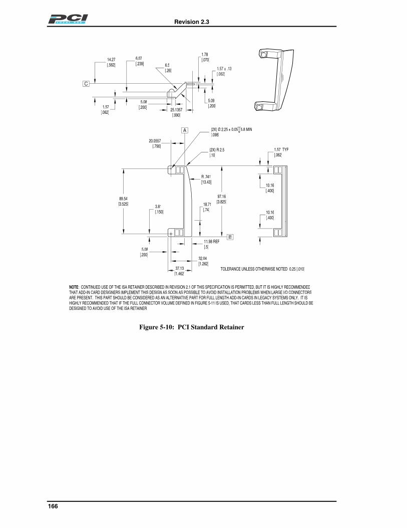
Revision 2.3
166
TOLERANCE UNLESS OTHERWISE NOTED 0.25 [.010]
10.16[.400]
10.16[.400]
1.57 TYP[.062]
18.71[.74]
R .341[13.43]
97.16[3.825]
(2X) R 2.5[.10]
(2X) Ø 2.25 ± 0.05 5.8 MIN.[.098]
11.98 REF[.5]5.08
[.200]32.04[1.262]
3.81[.150]
89.54[3.525]
20.0557[.790]
5.09[.200]
1.78[.070]
5.08[.200] 25.1357
[.990]
6.5[.26]
6.07[.239]
1.57[.062]
14.27[.562]
37.13[1.462]
NOTE: CONTINUED USE OF THE ISA RETAINER DESCRIBED IN REVISION 2.1 OF THIS SPECIFICATION IS PERMITTED, BUT IT IS HIGHLY RECOMMENDEDTHAT ADD-IN CARD DESIGNERS IMPLEMENT THIS DESIGN AS SOON AS POSSIBLE TO AVOID INSTALLATION PROBLEMS WHEN LARGE I/O CONNECTORSARE PRESENT. THIS PART SHOULD BE CONSIDERED AS AN ALTERNATIVE PART FOR FULL LENGTH ADD-IN CARDS IN LEGACY SYSTEMS ONLY. IT ISHIGHLY RECOMMENDED THAT IF THE FULL CONNECTOR VOLUME DEFINED IN FIGURE 5-11 IS USED, THAT CARDS LESS THAN FULL LENGTH SHOULD BEDESIGNED TO AVOID USE OF THE ISA RETAINER.
C
B
A
1.57 ± .13[.062]
Figure 5-10: PCI Standard Retainer

Revision 2.3
167
0.35
[.014
]
88.9
[3.5
0]
25.4
[1.0
]
NOTE
S:
1IT
IS H
IGHL
Y RE
COM
MEN
DED
FOR
ADD-
IN C
ARD
DESI
GNER
S TO
LOC
ATE
THEI
R I/O
CON
NECT
ORS
WIT
HTH
E 81
.9m
m L
ENGT
H TO
ENC
OMPA
SS L
EGAC
Y SY
STEM
S
IT IS
HIG
HLY
RECO
MM
ENDE
D TH
AT S
YSTE
M D
ESIG
NERS
IMPL
EMEN
T TH
E 88
.9m
m L
ENGT
H I/O
WIN
DOW
AS
SOON
AS P
OSSI
BLE
TO A
CCOM
MOD
ATE
THE
NEW
MUL
TI-P
ORT
ADD-
IN C
ARD
DESI
GNS.
2 3SY
STEM
S BU
ILT
AFTE
R JU
LY 1
997
MUS
T CO
MPL
Y W
ITH
THE
NEW
88.
9mm
LEN
GTH
I/O W
INDO
W.
TOLE
RANC
E UN
LESS
OTH
ERW
ISE
NOTE
D ±
0.25
[0.0
10]
10 [.39]
210
.16
[.40]
INSI
DE S
URFA
CE
3
23
R 88
.9[3
.50]
20 [.79]
LEGA
CY
313
.62
[.356
] IN
SIDE
SUR
FACE
1
25.4
[1.0
]
81.9
[3.2
24]
13
0.35
[.014
]
DETA
ILA
DETA
ILA
12.0
6[.4
7]
4AD
D-IN
CAR
DS U
SING
THE
FUL
L EX
TENT
OF
THIS
CONN
ECTO
R VO
LUM
E SH
OULD
DES
IGN
CARD
S US
ING
LESS
THAN
FUL
L LE
NGTH
AND
NOT
USE
THE
ISA
RETA
INER
.
Figure 5-11: I/O Window Height

Revision 2.3
168
Figure 5-12: Add-in Card Installation with Large I/O Connector

Revision 2.3
169
5.3. Connector Physical DescriptionThere are four connectors that can be used depending on the PCI implementation. Thedifferences between connectors are 32 bit and 64 bit, and the 3.3V and 5V signalingenvironments. A key differentiates the signaling environment voltages. The samephysical connector is used for the 32-bit signaling environments. In one orientation, thekey accepts 3.3V add-in cards. Rotated 180 degrees, the connector accepts 5V signalingadd-in cards. The pin numbering of the connector changes for the different signalingenvironments to maintain the same relative position of signals on the connector (seeFigures 5-14, 5-15, 5-17, and 5-19 for system board layout details).
In the connector drawings, the recommended system board layout details are given asnominal dimensions. Layout detail tolerancing should be consistent with the connectorsupplier's recommendations and good engineering practice.
See Figures 5-13 through 5-19 for connector dimensions and layout recommendations.See Figures 5-20 through 5-24 for card edge connector dimensions and tolerances.Tolerances for add-in cards are given so that interchangeable add-in cards can bemanufactured.

Revision 2.3
170
84.8
4[3
.40]
(2X)
4.5
7[.1
80]
(6X)
3.4
3[.1
35]
11.4
3[.4
50]
FITS
CAR
DS63
.25
[2.4
90]
1.27
[.050
]
1.27
[.050
]
4.41
[.174
]
1.57
±.0
2[.0
62 ±
.008
]
7.62
[.300
]9.02
MAX
[.355
]
81.2
8[3
.200
]
2.54
[.100
]
17.3
9[.6
85]
14.9
9[.5
90]
1.78
[.070
]
2.41
[.095
]
1.57
±.2
0b[.0
62 ±
.008
]
2.54
[.100
]
Figure 5-13: 32-bit Connector
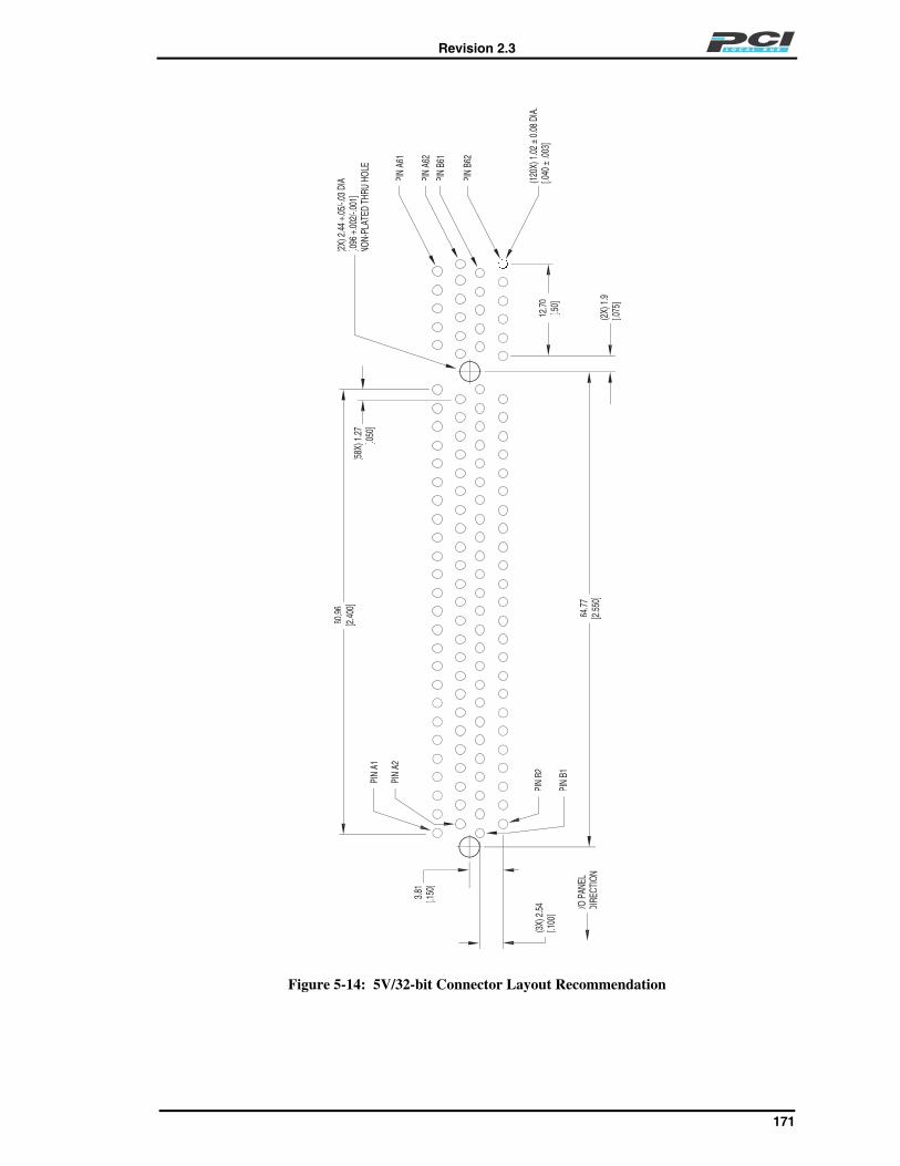
Revision 2.3
171
64.7
7[2
.550
](2
X) 1
.9[.0
75]
I/O P
ANEL
DIRE
CTIO
N
PIN
B2
PIN
B1
3.81
[.150
]
(3X)
2.5
4[.1
00]
PIN
A1
60.9
6[2
.400
](5
8X) 1
.27
[.050
]
(2X)
2.4
4 +.
05/-.
03 D
IA[.0
96 +
.002
/-.00
1]NO
N-PL
ATED
THR
U HO
LE
PIN
A61
PIN
B61
PIN
A62
PIN
B62
12.7
0[.5
0]
PIN
A2
(120
X) 1
.02
± 0.
08 D
IA.
[.040
± .0
03]
Figure 5-14: 5V/32-bit Connector Layout Recommendation

Revision 2.3
172
60.9
6[2
.400
]
(2X)
2.4
4 +.
05/-.
03 D
IA[.0
96 +
.002
/-.00
1]NO
N-PL
ATED
THR
U HO
LE
PIN
A1
PIN
B1
PIN
A2
PIN
B2
PIN
B62
PIN
B61
±.0
8 DI
A.[.0
40 ±
.003
]
3.81
[.150
]
(2X)
2.5
4[.1
00]
12.7
0[.5
00]
(58X
) 1.2
7[.0
50]
I/O P
ANEL
DIRE
CTIO
N64
.77
[2.5
50]
PIN
A62
PIN
A61
(2X)
1.9
1[.0
75]
Figure 5-15: 3.3V/32-bit Connector Layout Recommendation

Revision 2.3
173
43.1
8[1
.700
]
(8X)
3.4
3[.1
35]
58.1
7[2
.290
]
64.7
7[2
.550
]
1.27
[.050
]
FITS
CAR
DS
[.062
±.0
08]
7.62
[.300
]
9.02
MAX
[.355
]
(3X)
4.5
7[.1
80]
81.2
8[3
.200
]
2.54
[.100
]
17.3
9[.6
85]
128.
02[5
.040
]
14.9
9[.5
90]
1.78
[.070
]
2.41
[.095
]
1.78
±.0
3[.0
70 ±
.001
]1.
37 ±
.08
[.054
±.0
03]
Figure 5-16: 5V/64-bit Connector

Revision 2.3
174
(3X)
2.4
4 +0
5/-.0
3 DI
A[.0
96] +
.002
/-.00
1NO
N-PL
ATED
THR
U HO
LE PIN
A1
PIN
A2
PIN
B1
PIN
B2
3.81
[.150
]
(3X)
2.5
4[.1
00]
I/O P
ANEL
DIRE
CTIO
N[2
.55]
64.7
7
60.9
6[2
.400
](8
8X) 1
.27
[.050
]PI
N A6
1PI
N A6
2
(2X)
1.9
1[.0
75]
12.7
0[.5
00]
59.6
9[2
.350
]
39.3
7[.5
50]
PIN
B61
PIN
B62
PIN
B93
PIN
B94
PIN
A93
PIN
A94
(184
X) 1
.02
±.0
8 DI
A[.0
40]
±.0
03
1.91
[.075
]
Figure 5-17: 5V/64-bit Connector Layout Recommendation

Revision 2.3
175
FITS
CAR
DS1.
57 ±
.02
[.062
±.0
08]
7.62
[.300
]
9.02
MAX
[.355
] (3X)
4.5
7[.1
80]
107.
95[4
.250
]
64.7
7[2
.550
]18
.29
[.720
]
2.54
[.100
]
(8X)
1.5
2[.0
60]
15.4
9[.6
10]
128.
02[5
.040
]
63.2
[2.4
88]
14.9
9[.5
90]
16.2
9[.6
41]
2 [.0
79]2.
41[.0
95]
1.78
±.0
3±
1.37
±.0
8±
41.8
6[1
.648
]
Figure 5-18: 3.3V/64-bit Connector

Revision 2.3
176
(5X)
1.9
1[.0
75]
60.9
6[2
.400
]
PIN
A62
43.1
8[1
.700
]
12.7
0[.5
00]
39.3
7[1
.550
]
PIN
B2
PIN
B62
PIN
B61
PIN
B1
PIN
A2
PIN
A1
(88X
) 1.2
7[.0
50]
I/O P
ANEL
DIRE
CTIO
N64
.77
[2.5
50]
PIN
B94
(3X)
2.4
4 +.
05/-.
03 D
IA[.0
96 +
.002
/-.00
1]NO
N-PL
ATED
THRU
HOL
E
PIN
B93
3.81
[.150
]
(3X)
2.5
4[.1
00]
PIN
A94
PIN
A93
PIN
A61
(184
X) 1
.02
±.0
8 DI
A.[.0
40 ±
.003
]
Figure 5-19: 3.3V/64-bit Connector Layout Recommendation

Revision 2.3
177
63.7
[2.5
08]
15.4
4[0
.608
]
0.05
[0.0
02]
M MA
0.15
[0.0
06]
TYPI
CAL
ALL
TABS
BOTH
SID
ES T
AB T
O TA
B
BOTH
SID
ES T
AB T
O DA
TUM
TYPI
CAL
ALL
TABS
B14
B62
O.38
1X45
˚ CHA
MFE
R TY
P[0
.015
]
(2X)
0.9
27 ±
0.02
5[0
.036
±0.
001]
32 B
IT /
3 VO
LT2
X 60
CON
NECT
OR
(2X)
COM
PONE
NTSI
DE B
B11
12.7
[0.5
00]
60.9
7[2
.400
]
56.2
1[2
.213
]
O.38
1X45
˚
B01
1.27
[0.0
50]
62.8
7[2
.475
]
AA
1.91
[0.0
75]
14.6
1[0
.575
]
TO
LER
AN
CE
UN
LES
S O
TH
ER
WIS
E N
OT
ED
±0.
25 [0
.010
]
Figure 5-20: 3.3V/32-bit Add-in Card Edge Connector Dimensions and Tolerances

Revision 2.3
178
63.7
[2.5
08]
15.4
4[0
.608
]
106.
88[4
.208
]
0.05
[0.0
02]
M MA
0.15
[0.0
06]
TYPI
CAL
ALL
TABS
BOTH
SID
ES T
AB T
O TA
B
BOTH
SID
ES T
AB T
O DA
TUM
TYPI
CAL
ALL
TABS
65.8
4[2
.592
]
B14
B62
O.38
1X45
˚[0
.015
] CH
AMFE
R TY
P
(2X)
0.9
27 ±
0.02
5[0
.036
±0.
001]
B1
64 B
IT /
3 VO
LT2
X 92
CON
NECT
OR
(2X)
106.
06[4
.175
]
B63
B94
COM
PONE
NTSI
DE B
39.3
7[1
.550
]
B11
12.7
[0.5
00]
60.8
7[2
.475
]
62.8
7[2
.475
]
66.6
8[2
.625
]
56.2
1[2
.213
]
1.91
[0.0
75]
1.27
[0.0
50]
AA
14.6
1[0
.575
]
TO
LER
AN
CE
UN
LES
S O
TH
ER
WIS
E N
OT
ED
± 0
.25
[0.0
10]
Figure 5-21: 3.3V/64-bit Add-in Card Edge Connector Dimensions and Tolerances

Revision 2.3
179
48.2
[1.9
0]15
.44
[0.6
08]
63.7
[2.5
08]
44.4
5[1
.750
]
1.91
[.075
]
46.3
5[1
.825
]12
.7[.5
00]
(2X)
50.1
7[1
.975
]14
.61
[.575
]12
.7[.5
00]
56.2
1[2
.213
]62
.87
[2.4
75]
1.27
[.050
]
32 B
IT /
UNIV
ERSA
L2
X 60
CON
NECT
OR
(4X)
0.9
27 ±
0.02
5[0
.036
±
[0.0
15]
CHAM
FER
TYP
O.38
1X45
˚
B01
B11
B14
B49
B52
B62
BOTH
SID
ES T
AB T
O DA
TUM
BOTH
SID
ES T
AB T
O TA
BTY
PICA
L AL
L TA
BS
0.15
[0.0
06]
AMM
0.05
[0.0
02]
COM
PONE
NTSI
DE B
A AT
OLE
RA
NC
E U
NLE
SS
OT
HE
RW
ISE
NO
TE
D ±
0.25
[0.0
10]
Figure 5-22: Universal 32-bit Add-in Card Edge Connector Dimensions and Tolerances

Revision 2.3
180
48.2
[1.9
0]
15.4
4[0
.608
]
63.7
[2.5
08]
65.8
4[2
.592
]
106.
88[4
.208
]
44.4
5[1
.750
]
1.91
[.075
]
46.3
5[1
.825
]12
.7[.5
00]
(2X)
50.1
7[1
.975
]14
.61
[.575
]
12.7
[.500
]1.
27[.0
50]
56.2
1[2
.213
]62
.87
[2.4
75]
39.3
7[1
.550
]
106.
06[4
.176
]
64 B
IT /
UNIV
ERSA
L2
X 92
CON
NECT
OR
(4X)
0.9
27 ±
0.02
5[0
.036
±0.
001]
[0.0
15]
CHAM
FER
TYP
O.38
1X45
˚
B01
B94
B11
B14
B49
B52
B62
B63
TYPI
CAL
ALL
TABS
BOTH
SID
ES T
AB T
O DA
TUM
BOTH
SID
ES T
AB T
O TA
BTY
PICA
L AL
L TA
BS
0.15
[0.0
06]
AMM
0.05
[0.0
02]
COM
PONE
NTSI
DE B
A AT
OLE
RA
NC
E U
NLE
SS
OT
HE
RW
ISE
NO
TE
D ±
0.2
5 [0
.010
]
Figure 5-23: Universal 64-bit Add-in Card Edge Connector Dimensions and Tolerances

Revision 2.3
181
CRITICAL CONTACT AREA
0.25 ± 0.13[.010 ± 0.005](OPTIONAL)
TYP BOTH SIDES
5.18 ± 0.13[0.20 ± 0.005]
12.07 ± 0.13[.475 ± 0.005]
6.35 ± 0.13[.250 ± 0.005]
9.52 ± 0.13[.380 ± 0.005]
0.508 ± 0.025±
TYP BOTH SIDES
0.508 ± 0.025
TYP BOTH SIDES
R TYPBOTH SIDES(OPTIONAL)
B
1.27[0.050]
Figure 5-24: PCI Add-in Card Edge Connector Contacts
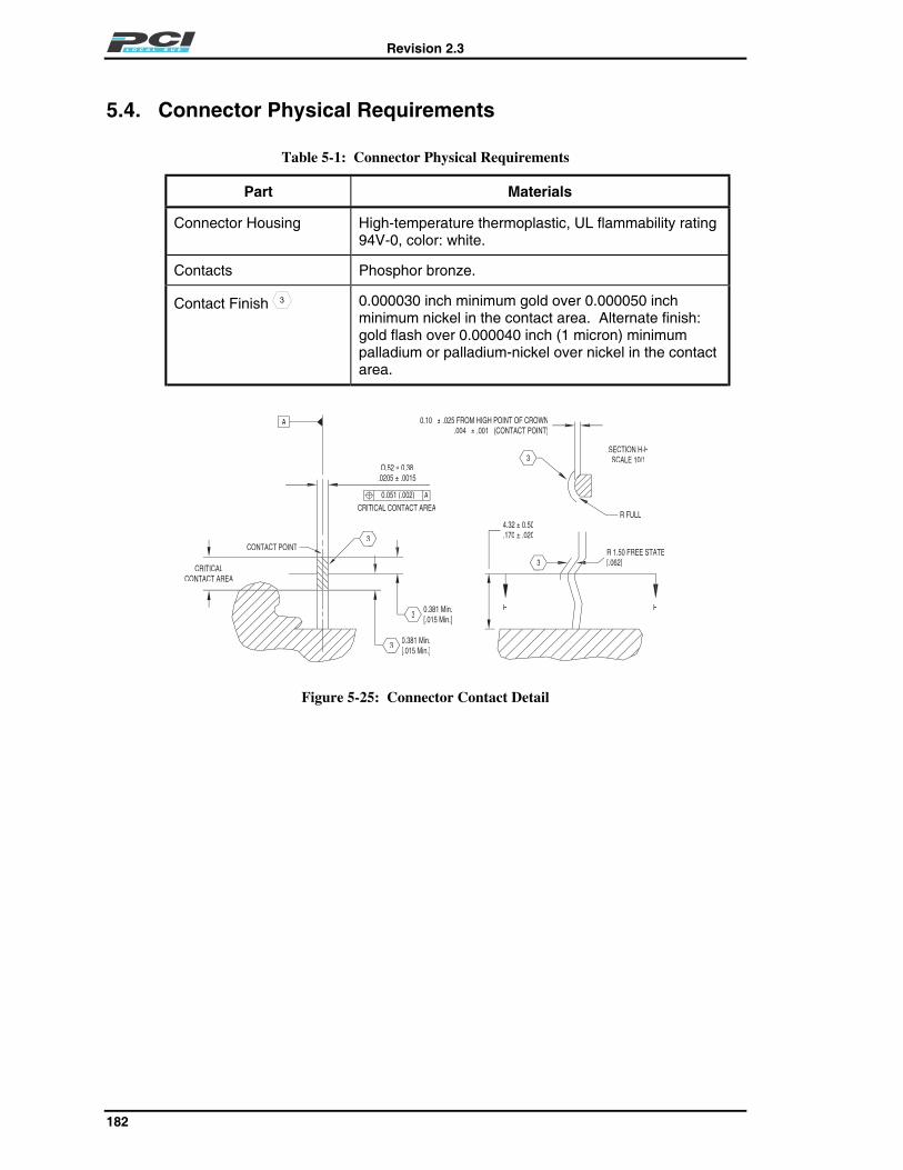
Revision 2.3
182
5.4. Connector Physical Requirements
Table 5-1: Connector Physical Requirements
Part Materials
Connector Housing High-temperature thermoplastic, UL flammability rating94V-0, color: white.
Contacts Phosphor bronze.
Contact Finish 3 0.000030 inch minimum gold over 0.000050 inchminimum nickel in the contact area. Alternate finish:gold flash over 0.000040 inch (1 micron) minimumpalladium or palladium-nickel over nickel in the contactarea.
0.051 (.002) A
O.52 ± 0.38±
CONTACT POINT
A
CRITICAL CONTACT AREA
CRITICALCONTACT AREA
0.381 Min.[.015 Min.]
0.381 Min.[.015 Min.]
H H
R 1.50 FREE STATE[.062]
SECTION H-HSCALE 10/1
R FULL
0.10 ± .025 FROM HIGH POINT OF CROWN.004 ± .001 (CONTACT POINT)
4.32 ± 0.50.170 .020
3
3
3
3
3
Figure 5-25: Connector Contact Detail

Revision 2.3
183
5.5. Connector Performance Specification
Table 5-2: Connector Mechanical Performance Requirements
Parameter Specification
Durability 100 mating cycles without physical damage orexceeding low level contact resistance requirementwhen mated with the recommended add-in card edge.
Mating Force 6 oz. (1.7 N) max. avg. per opposing contact pair usingMIL-STD-1344, Method 2013.1 and gauge perMIL-C-21097 with profile as shown in add-in cardspecification.
Contact Normal Force 75 grams minimum.
Table 5-3: Connector Electrical Performance Requirements
Parameter Specification
Contact Resistance (low signal level) 30 mΩ max. initial, 10 mΩ max.increase through testing. Contact resistance, test perMIL-STD-1344, Method 3002.1.
Insulation Resistance 1000 MΩ min. per MIL STD 202, Method 302,Condition B.
Dielectric WithstandVoltage
500 VAC RMS. per MIL-STD-1344, Method D3001.1Condition 1.
Capacitance 2 pF max. @ 1 MHz.
Current Rating 1 A, 30 °C rise above ambient.
Voltage Rating 125 V.
Certification UL Recognition and CSA Certification required.
Table 5-4: Connector Environmental Performance Requirements
Parameter Specification
Operating Temperature -40 °C to 105 °C
Thermal Shock -55 °C to 85 °C, 5 cycles per MIL-STD-1344, Method1003.1.
Flowing Mixed Gas Test Battelle, Class II. Connector mated with an add-in cardand tested per Battelle method.

Revision 2.3
184
5.6. System Board ImplementationTwo types of system board implementations are supported by the PCI add-in card design:add-in card connectors mounted on the system board and add-in card connectors mountedon a riser card.
See Figure 5-26 for system board details. The system board drawing shows the relativelocations of the PCI 3.3V and 5V connector datums. Both 3.3V and 5V connectors areshown on the system board to concisely convey the dimensional information.Frequently, a given system would incorporate either the 3.3V or the 5V PCI connector,but not both. The standard card spacing for PCI connectors is 0.8 inches.
See Figures 5-27, 5-28, 5-29, 5-30, 5-31, 5-32, and 5-33 for riser card details. In theconnector drawings and riser connector footprints, the details are given as nominaldimensions. The tolerances should be consistent with the connector supplier’srecommendations and good engineering practice.

Revision 2.3
185
BULK
HEAD
LOCA
TION
3.3V
PCI
CONN
ECTO
R
5V P
CICO
NNEC
TOR
REST
RICT
EDCO
MPO
NENT
HEI
GHT
5.08
[.20
0] M
AX88
.90
[3.5
0] M
AX.
61.4
7 [2
.42]
MIN
.VA
RIAB
LE S
HORT
CAR
D SL
OT
SHOR
T CA
RD S
LOT
70.1
0 [2
.76]
MIN
.
207.
52 [8
.17]
MIN
LO
NG C
ARD
SLOT
REST
RICT
ED C
OMPO
NENT
HEIG
HT 1
5.24
[.60
0] M
AX.
20.3
2 [.8
00]
20.3
2 [.8
00]
8.89
[.35
2]
48.2
[1.9
0]61
.47
[2.4
20]
REST
RICT
ED C
OMPO
NENT
HEI
GHT
5.08
[.20
0] M
AX. O
N 32
BIT
PLA
NAR
FOR
64-B
IT C
ARD
INTE
ROPE
RABI
LITY
3.3V
PCI
PRI
MAR
YRE
FERE
NCE
DATU
M5V
PCI
PRI
MAR
YRE
FERE
NCE
DATU
M
TO
LER
AN
CE
UN
LES
S O
TH
ER
WIS
E N
OT
ED
± 0
.25
[0.0
10]
Figure 5-26: PCI Connector Location on System Board

Revision 2.3
186
84.8
4[3
.40]
(2X)
4.5
7[.1
80]
(6X)
3.4
3[.1
35]
11.4
3[.4
50]
FITS
CAR
DS63
.25
[2.4
90]
1.27
[.050
]
1.27
[.050
]
4.41
[.174
]
1.57
±.0
2[.0
62 ±
.008
]
7.62
[.300
]9.02
MAX
[.355
]
81.2
8[3
.200
]
2.54
[.100
]
17.3
9[.6
85]
14.9
9[.5
90]
1.78
[.070
]
2.41
[.095
]
1.78
±.0
3[.0
70 ±
.001
]
2.54
[.100
]
Figure 5-27: 32-bit PCI Riser Connector38
38 It is highly recommended that LPX system chassis designers utilize the PCI riser connector whenimplementing riser cards on LPX systems and using connectors on 0.800-inch spacing.
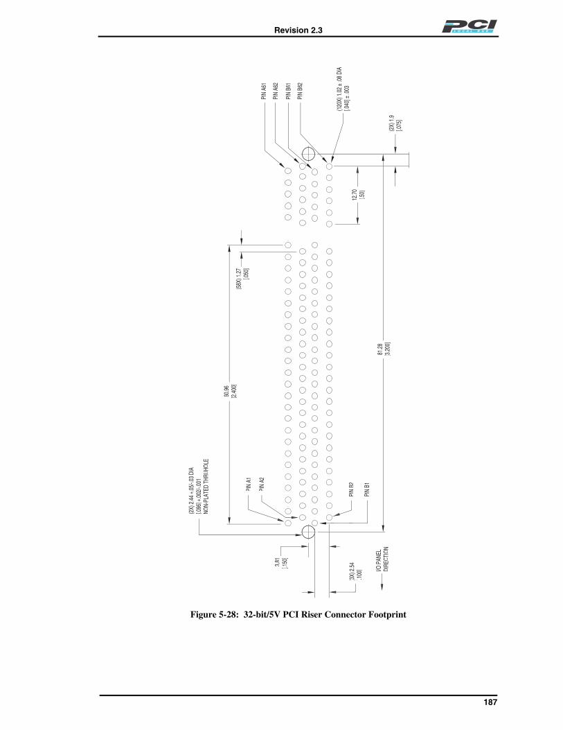
Revision 2.3
187
81.2
8[3
.200
](2
X) 1
.9[.0
75]
I/O P
ANEL
DIRE
CTIO
N
PIN
B2
PIN
B1
3.81
[.150
]
(3X)
2.5
4[.1
00]
PIN
A1
60.9
6[2
.400
](5
8X) 1
.27
[.050
]
(2X)
2.4
4 +.
05/-.
03 D
IA[.0
96] +
.002
/-.00
1NO
N-PL
ATED
THR
UHOL
E
PIN
A61
PIN
B61
PIN
A62
PIN
B62
12.7
0[.5
0]
PIN
A2
(120
X) 1
.02
± .0
8 DI
A[.0
40] ±
.003
Figure 5-28: 32-bit/5V PCI Riser Connector Footprint

Revision 2.3
188
60.9
6[2
.400
]
(2X)
2.4
4 +.
05/-.
03 D
IA[.0
96 +
.002
/-.00
1]NO
N-PL
ATED
THR
U HO
LE
PIN
A1
PIN
B1
PIN
A2
PIN
B2PI
N B6
2
PIN
B61
±.0
8 DI
A.[.0
40 ±
.003
]
3.81
[.150
]
(3X)
2.5
4[.1
00]
12.7
0[.5
00]
(58X
) 1.2
7[.0
50]
I/O P
ANEL
DIRE
CTIO
N81
.28
[3.2
00]
PIN
A62
PIN
A61
(2X)
1.9
[.075
]
Figure 5-29: 32-bit/3.3V PCI Riser Connector Footprint

Revision 2.3
189
43.1
8[1
.700
]
(8X)
3.4
3[.1
35]
58.1
7[2
.290
]
64.7
7[2
.550
]
1.27
[.050
]
FITS
CAR
DS
[.062
±.0
08]
7.62
[.300
]
9.02
MAX
[.355
]
(3X)
4.5
7[.1
80]
81.2
8[3
.200
]
2.54
[.100
]
17.3
9[.6
85]
128.
02[5
.040
]
14.9
9[.5
90]
1.78
[.070
]
2.41
[.095
]
1.78
±.0
3[.0
70 ±
.001
]1.
37 ±
.08
[.054
±.0
03]
Figure 5-30: 64-bit/5V PCI Riser Connector38

Revision 2.3
190
(3X)
2.4
4 +0
5/-.0
3 DI
A[.0
96 +
.002
/-.00
1]NO
N-PL
ATED
THR
U HO
LE PIN
A1
PIN
A2
PIN
B1
PIN
B2
3.81
[.150
]
(3X)
2.5
4[.1
00]
I/O P
ANEL
DIRE
CTIO
N[3
.200
]81
.28
60.9
6[2
.400
](8
8X) 1
.27
[.050
]PI
N A6
1
PIN
A62
(2X)
1.9
1[.0
75]
12.7
0[.5
00]
43.1
8[1
.700
]
39.3
7[.5
50]
PIN
B61
PIN
B62
PIN
B93
PIN
B94
PIN
A93
PIN
A94
(184
X) 1
.02
±[.0
40 ±
.003
]
1.91
[.07
5]
Figure 5-31: 64-bit/5V PCI Riser Connector Footprint

Revision 2.3
191
FITS
CAR
DS1.
57
.02
[.062
±.0
08]
7.62
[.300
]
9.02
MAX
[.355
]
(3X)
4.5
7[.1
80]
124.
46[4
.900
]
81.2
8[3
.200
]
2.54
[.100
]
(8X)
1.5
2[.0
62]
17.3
9[.6
85]
128.
02[5
.040
]
63.2
[2.4
88]
14.9
9[.5
90]
1.78
[.070
]
2.41
[.095
]
1.78
± .0
3[.0
70 ±
.001
]1.
37 ±
.08
[.054
±.0
03]
41.8
6[1
.648
]
Figure 5-32: 64-bit/3.3V PCI Riser Connector38

Revision 2.3
192
(2X)
1.9
1[.0
75]
77.4
7[3
.050
]
PIN
A62
43.1
8[1
.700
]
12.7
0[.5
00]
39.3
7[1
.550
]
PIN
B2
PIN
B94
(3X)
2.4
4 +.
05/-.
03 D
IA[.0
96 +
.002
/-.00
1]NO
N-PL
ATED
THRU
HOL
E
PIN
B93
PIN
B62
PIN
B61
3.81
[.150
]
(3X)
2.5
4[.1
00]
PIN
B1
PIN
A2
PIN
A1
(88X
) 1.2
7[.0
50]
I/O P
ANEL
DIRE
CTIO
N81
.28
[3.2
00]
PIN
A94
PIN
A93
PIN
A61
(184
X) 1
.02
±.0
8 DI
A.[.0
40 ±
.003
]
Figure 5-33: 64-bit/3.3V PCI Riser Connector Footprint

Revision 2.3
193
Chapter 6Configuration Space
This chapter defines the programming model and usage rules for the configurationregister space in PCI compliant devices. This chapter is limited to the definition of PCIcompliant components for a wide variety of system types. System dependent issues forspecific platforms, such as mapping various PCI address spaces into host CPU addressspaces, access ordering rules, requirements for host-to-PCI bus bridges, etc., are notdescribed in this chapter.
The intent of the PCI Configuration Space definition is to provide an appropriate set ofconfiguration "hooks" which satisfies the needs of current and anticipated systemconfiguration mechanisms, without specifying those mechanisms or otherwise placingconstraints on their use. The criteria for these configuration "hooks" are:
• Sufficient support to allow future configuration mechanisms to provide:
• Full device relocation, including interrupt binding
• Installation, configuration, and booting without user intervention
• System address map construction by device independent software
• Minimize the silicon burden created by required functions
• Leverage commonality with a template approach to common functions, withoutprecluding devices with unique requirements
All PCI devices (except host bus bridges) must implement Configuration Space.Multifunction devices must provide a Configuration Space for each functionimplemented (refer to Section 6.2.1.).

Revision 2.3
194
6.1. Configuration Space OrganizationThis section defines the organization of Configuration Space registers and imposes aspecific record structure or template on the 256-byte space. This space is divided into apredefined header region and a device dependent region.39 Devices implement only thenecessary and relevant registers in each region. A device's Configuration Space must beaccessible at all times, not just during system boot.
The predefined header region consists of fields that uniquely identify the device andallow the device to be generically controlled. The predefined header portion of theConfiguration Space is divided into two parts. The first 16 bytes are defined the same forall types of devices. The remaining bytes can have different layouts depending on thebase function that the device supports. The Header Type field (located at offset 0Eh)defines what layout is provided. Currently three Header Types are defined, 00h whichhas the layout shown in Figure 6-1, 01h which is defined for PCI-to-PCI bridges and isdocumented in the PCI to PCI Bridge Architecture Specification, and 02h which isdefined for CardBus bridges and is documented in the PC Card Standard40.
System software may need to scan the PCI bus to determine what devices are actuallypresent. To do this, the configuration software must read the Vendor ID in each possiblePCI "slot." The host bus to PCI bridge must unambiguously report attempts to read theVendor ID of non-existent devices. Since 0FFFFh is an invalid Vendor ID, it is adequatefor the host bus to PCI bridge to return a value of all 1's on read accesses toConfiguration Space registers of non-existent devices. (Note that these accesses will beterminated with a Master-Abort.)
All PCI devices must treat Configuration Space write operations to reserved registers asno-ops; that is, the access must be completed normally on the bus and the data discarded.Read accesses to reserved or unimplemented registers must be completed normally and adata value of 0 returned.
Figure 6-1 depicts the layout of a Type 00h predefined header portion of the 256-byteConfiguration Space. Devices must place any necessary device specific registers after thepredefined header in Configuration Space. All multi-byte numeric fields follow little-endian ordering; that is, lower addresses contain the least significant parts of the field.Software must take care to deal correctly with bit-encoded fields that have some bitsreserved for future use. On reads, software must use appropriate masks to extract thedefined bits, and may not rely on reserved bits being any particular value. On writes,software must ensure that the values of reserved bit positions are preserved; that is, thevalues of reserved bit positions must first be read, merged with the new values for otherbit positions and the data then written back. Section 6.2. describes the registers in theType 00h predefined header portion of the Configuration Space.
39 The device dependent region contains device specific information and is not described in this document.
40 The PC Card Standard is available from PCMCIA and contact information can be found athttp://www.pc-card.com

Revision 2.3
195
Figure 6-1: Type 00h Configuration Space Header
All PCI compliant devices must support the Vendor ID, Device ID, Command, Status,Revision ID, Class Code, and Header Type fields in the header. Refer to Section 6.2.4.for the requirements for Subsystem ID and Subsystem Vendor ID. Implementation of theother registers in a Type 00h predefined header is optional (i.e., they can be treated asreserved registers) depending on device functionality. If a device supports the functionthat the register is concerned with, the device must implement it in the defined locationand with the defined functionality.
Revision 2.3
196
6.2. Configuration Space FunctionsPCI has the potential for greatly increasing the ease with which systems may beconfigured. To realize this potential, all PCI devices must provide certain functions thatsystem configuration software can utilize. This section also lists the functions that needto be supported by PCI devices via registers defined in the predefined header portion ofthe Configuration Space. The exact format of these registers (i.e., number of bitsimplemented) is device specific. However, some general rules must be followed. Allregisters must be capable of being read, and the data returned must indicate the value thatthe device is actually using.
Configuration Space is intended for configuration, initialization, and catastrophic errorhandling functions. Its use should be restricted to initialization software and errorhandling software. All operational software must continue to use I/O and/or MemorySpace accesses to manipulate device registers.
6.2.1. Device Identification
Five fields in the predefined header deal with device identification. All PCI devices arerequired to implement these fields. Generic configuration software will be able to easilydetermine what devices are available on the system's PCI bus(es). All of these registersare read-only.
Vendor ID This field identifies the manufacturer of the device. Validvendor identifiers are allocated by the PCI SIG to ensureuniqueness. 0FFFFh is an invalid value for Vendor ID.
Device ID This field identifies the particular device. This identifier isallocated by the vendor.
Revision ID This register specifies a device specific revision identifier.The value is chosen by the vendor. Zero is an acceptablevalue. This field should be viewed as a vendor definedextension to the Device ID.
Header Type This byte identifies the layout of the second part of thepredefined header (beginning at byte 10h in ConfigurationSpace) and also whether or not the device contains multiplefunctions. Bit 7 in this register is used to identify a multi-function device. If the bit is 0, then the device is singlefunction. If the bit is 1, then the device has multiple functions.Bits 6 through 0 identify the layout of the second part of thepredefined header. The encoding 00h specifies the layoutshown in Figure 6-1. The encoding 01h is defined for PCI-to-PCI bridges and is defined in the document PCI to PCI BridgeArchitecture Specification. The encoding 02h is defined for aCardBus bridge and is documented in the PC Card Standard.All other encodings are reserved.

Revision 2.3
197
Class Code The Class Code register is read-only and is used to identify thegeneric function of the device and, in some cases, a specificregister-level programming interface. The register is brokeninto three byte-size fields. The upper byte (at offset 0Bh) is abase class code which broadly classifies the type of functionthe device performs. The middle byte (at offset 0Ah) is a sub-class code which identifies more specifically the function ofthe device. The lower byte (at offset 09h) identifies a specificregister-level programming interface (if any) so that deviceindependent software can interact with the device. Encodingsfor base class, sub-class, and programming interface areprovided in Appendix D. All unspecified encodings arereserved.
6.2.2. Device Control
The Command register provides coarse control over a device's ability to generate andrespond to PCI cycles. When a 0 is written to this register, the device is logicallydisconnected from the PCI bus for all accesses except configuration accesses. Alldevices are required to support this base level of functionality. Individual bits in theCommand register may or may not be implemented depending on a device’sfunctionality. For instance, devices that do not implement an I/O Space will notimplement a writable element at bit location 0 of the Command register. Devicestypically power up with all 0's in this register, but Section 6.6. explains some exceptions.Figure 6-2 shows the layout of the register and Table 6-1 explains the meanings of thedifferent bits in the Command register.
Interrupt Disable
01234
Reserved
515 678
IO Space
910
Fast Back-to-Back EnableSERR# EnableReservedParity Error ResponseVGA Palette SnoopMemory Write and Invalidate EnableSpecial CyclesBus MasterMemory Space
Figure 6-2: Command Register Layout

Revision 2.3
198
Table 6-1: Command Register Bits
Bit Location Description
0 Controls a device's response to I/O Space accesses. A value of 0disables the device response. A value of 1 allows the device torespond to I/O Space accesses. State after RST# is 0.
1 Controls a device's response to Memory Space accesses. A value of0 disables the device response. A value of 1 allows the device torespond to Memory Space accesses. State after RST# is 0.
2 Controls a device's ability to act as a master on the PCI bus. A valueof 0 disables the device from generating PCI accesses. A value of 1allows the device to behave as a bus master. State after RST# is 0.
3 Controls a device's action on Special Cycle operations. A value of 0causes the device to ignore all Special Cycle operations. A value of 1allows the device to monitor Special Cycle operations. State afterRST# is 0.
4 This is an enable bit for using the Memory Write and Invalidatecommand. When this bit is 1, masters may generate the command.When it is 0, Memory Write must be used instead. State after RST#is 0. This bit must be implemented by master devices that cangenerate the Memory Write and Invalidate command.
5 This bit controls how VGA compatible and graphics devices handleaccesses to VGA palette registers. When this bit is 1, palettesnooping is enabled (i.e., the device does not respond to paletteregister writes and snoops the data). When the bit is 0, the deviceshould treat palette write accesses like all other accesses. VGAcompatible devices should implement this bit. Refer to Section 3.10.for more details on VGA palette snooping.

Revision 2.3
199
Table 6-1: Command Register Bits (continued)
Bit Location Description
6 This bit controls the device's response to parity errors. When the bitis set, the device must take its normal action when a parity error isdetected. When the bit is 0, the device sets its Detected Parity Errorstatus bit (bit 15 in the Status register) when an error is detected, butdoes not assert PERR# and continues normal operation. This bit'sstate after RST# is 0. Devices that check parity must implement thisbit. Devices are still required to generate parity even if paritychecking is disabled.
7 Hardwire this bit to 0.41
8 This bit is an enable bit for the SERR# driver. A value of 0 disablesthe SERR# driver. A value of 1 enables the SERR# driver. This bit'sstate after RST# is 0. All devices that have an SERR# pin mustimplement this bit. Address parity errors are reported only if this bitand bit 6 are 1.
9 This optional read/write bit controls whether or not a master can dofast back-to-back transactions to different devices. Initializationsoftware will set the bit if all targets are fast back-to-back capable. Avalue of 1 means the master is allowed to generate fast back-to-backtransactions to different agents as described in Section 3.4.2. Avalue of 0 means fast back-to-back transactions are only allowed tothe same agent. This bit's state after RST# is 0.
10 This bit disables the device/function from asserting INTx#. A value of0 enables the assertion of its INTx# signal. A value of 1 disables theassertion of its INTx# signal. This bit’s state after RST# is 0. Refer toSection 6.8.1.3 for control of MSI.
11-15 Reserved.
41 This bit cannot be assigned any new meaning in new designs. In an earlier version of this specification,bit 7 was used and devices may have hardwired it to 0, 1, or implemented a read/write bit.

Revision 2.3
200
6.2.3. Device Status
The Status register is used to record status information for PCI bus related events. Thedefinition of each of the bits is given in Table 6-2 and the layout of the register is shownin Figure 6-3. Devices may not need to implement all bits, depending on devicefunctionality. For instance, a device that acts as a target, but will never signal Target-Abort, would not implement bit 11. Reserved bits should be read-only and return zerowhen read.
Reads to this register behave normally. Writes are slightly different in that bits can bereset, but not set. A one bit is reset (if it is not read-only) whenever the register iswritten, and the write data in the corresponding bit location is a 1. For instance, to clearbit 14 and not affect any other bits, write the value 0100_0000_0000_0000b to theregister.
15 14 13 12 11 10 9 8 7 6 5 4 3 0
Interrupt StatusCapabilities List66 MHz CapableReservedFast Back-to-Back CapableMaster Data Parity ErrorDEVSEL timing
00 - fast01 - medium10 - slow
Signaled Target AbortReceived Target AbortReceived Master AbortSignaled system ErrorDetected Parity Error
Reserved
Figure 6-3: Status Register Layout

Revision 2.3
201
Table 6-2: Status Register Bits
Bit Location Description
0-2 Reserved.
3 This read-only bit reflects the state of the interrupt in thedevice/function. Only when the Interrupt Disable bit in the commandregister is a 0 and this Interrupt Status bit is a 1, will thedevice’s/function’s INTx# signal be asserted. Setting the InterruptDisable bit to a 1 has no effect on the state of this bit.
4 This optional read-only bit indicates whether or not this deviceimplements the pointer for a New Capabilities linked list at offset 34h.A value of zero indicates that no New Capabilities linked list isavailable. A value of one indicates that the value read at offset 34h isa pointer in Configuration Space to a linked list of new capabilities.Refer to Section 6.7. for details on New Capabilities.
5 This optional read-only bit indicates whether or not this device iscapable of running at 66 MHz as defined in Chapter 7. A value of zeroindicates 33 MHz. A value of 1 indicates that the device is 66 MHzcapable.
6 This bit is reserved42.
7 This optional read-only bit indicates whether or not the target iscapable of accepting fast back-to-back transactions when thetransactions are not to the same agent. This bit can be set to 1 if thedevice can accept these transactions and must be set to 0 otherwise.Refer to Section 3.4.2. for a complete description of requirements forsetting this bit.
8 This bit is only implemented by bus masters. It is set when threeconditions are met: 1) the bus agent asserted PERR# itself (on aread) or observed PERR# asserted (on a write); 2) the agent settingthe bit acted as the bus master for the operation in which the erroroccurred; and 3) the Parity Error Response bit (Command register) isset.
9-10 These bits encode the timing of DEVSEL#. Section 3.6.1. specifiesthree allowable timings for assertion of DEVSEL#. These areencoded as 00b for fast, 01b for medium, and 10b for slow (11b isreserved). These bits are read-only and must indicate the slowesttime that a device asserts DEVSEL# for any bus command exceptConfiguration Read and Configuration Write.
42 In Revision 2.1 of this specification, this bit was used to indicate whether or not a device supported UserDefinable Features.

Revision 2.3
202
Table 6-2: Status Register Bits (continued)
Bit Location Description
11 This bit must be set by a target device whenever it terminates atransaction with Target-Abort. Devices that will never signal Target-Abort do not need to implement this bit.
12 This bit must be set by a master device whenever its transaction isterminated with Target-Abort. All master devices must implement thisbit.
13 This bit must be set by a master device whenever its transaction(except for Special Cycle) is terminated with Master-Abort. All masterdevices must implement this bit.
14 This bit must be set whenever the device asserts SERR#. Deviceswho will never assert SERR# do not need to implement this bit.
15 This bit must be set by the device whenever it detects a parity error,even if parity error handling is disabled (as controlled by bit 6 in theCommand register).
6.2.4. Miscellaneous Registers
This section describes the registers that are device independent and only need to beimplemented by devices that provide the described function.
CacheLine Size
This read/write register specifies the system cacheline size in units of DWORDs. Thisregister must be implemented by master devices that can generate the Memory Write andInvalidate command (refer to Section 3.1.1.). The value in this register is also used bymaster devices to determine whether to use Read, Read Line, or Read Multiplecommands for accessing memory (refer to Section 3.1.2.).
Slave devices that want to allow memory bursting using cacheline wrap addressing mode(refer to Section 3.2.2.2.) must implement this register to know when a burst sequencewraps to the beginning of the cacheline.
This field must be initialized to 0 at RST#.
A device may limit the number of cacheline sizes that it can support. For example, itmay accept only powers of 2 less than 128. If an unsupported value is written to theCacheLine Size register, the device should behave as if a value of 0 was written.
Latency Timer
This register specifies, in units of PCI bus clocks, the value of the Latency Timer for thisPCI bus master (refer to Section 3.5.4.). This register must be implemented as writableby any master that can burst more than two data phases. This register may beimplemented as read-only for devices that burst two or fewer data phases, but thehardwired value must be limited to 16 or less. A typical implementation would be tobuild the five high-order bits (leaving the bottom three as read-only), resulting in a timergranularity of eight clocks. At RST#, the register must be initialized to 0 (ifprogrammable).

Revision 2.3
203
Built-in Self Test (BIST)
This optional register is used for control and status of BIST. Devices that do not supportBIST must always return a value of 0 (i.e., treat it as a reserved register). A device whoseBIST is invoked must not prevent normal operation of the PCI bus. Figure 6-4 shows theregister layout and Table 6-3 describes the bits in the register.
7 6 5 4 0123
Rsvd
Start BISTBIST capable
Figure 6-4: BIST Register Layout
Table 6-3: BIST Register Bits
Bit Location Description
7 Return 1 if device supports BIST. Return 0 if the device is not BISTcapable.
6 Write a 1 to invoke BIST. Device resets the bit when BIST iscomplete. Software should fail the device if BIST is not complete after2 seconds.
5-4 Reserved. Device returns 0.
3-0 A value of 0 means the device has passed its test. Non-zero valuesmean the device failed. Device-specific failure codes can be encodedin the non-zero value.
CardBus CIS Pointer
This optional register is used by those devices that want to share silicon between CardBusand PCI. The field is used to point to the Card Information Structure (CIS) for theCardBus card.
For a detailed explanation of the CIS, refer to the PCMCIA v2.10 specification. Thesubject is covered under the heading Card Metaformat and describes the types ofinformation provided and the organization of this information.
Interrupt Line
The Interrupt Line register is an eight-bit register used to communicate interrupt linerouting information. The register is read/write and must be implemented by any device(or device function) that uses an interrupt pin. POST software will write the routinginformation into this register as it initializes and configures the system.
The value in this register tells which input of the system interrupt controller(s) thedevice's interrupt pin is connected to. The device itself does not use this value, rather it isused by device drivers and operating systems. Device drivers and operating systems can

Revision 2.3
204
use this information to determine priority and vector information. Values in this registerare system architecture specific.43
Interrupt Pin
The Interrupt Pin register tells which interrupt pin the device (or device function) uses. Avalue of 1 corresponds to INTA#. A value of 2 corresponds to INTB#. A value of 3corresponds to INTC#. A value of 4 corresponds to INTD#. Devices (or devicefunctions) that do not use an interrupt pin must put a 0 in this register. The values 05hthrough FFh are reserved. This register is read-only. Refer to Section 2.2.6. for furtherdescription of the usage of the INTx# pins.
MIN_GNT and MAX_LAT
These read-only byte registers are used to specify the device’s desired settings forLatency Timer values. For both registers, the value specifies a period of time in units of¼ microsecond. Values of 0 indicate that the device has no major requirements for thesettings of Latency Timers.
MIN_GNT is used for specifying how long a burst period the device needs assuming aclock rate of 33 MHz. MAX_LAT is used for specifying how often the device needs togain access to the PCI bus.
Devices should specify values that will allow them to most effectively use the PCI bus aswell as their internal resources. Values should be chosen assuming that the target doesnot insert any wait-states.
Implementation Example: Choosing MIN_GNT and MAX_LATA fast Ethernet controller (100 Mbs) has a 64-byte buffer for each transfer direction.Optimal usage of these internal resources is achieved when the device treats each bufferas two 32-byte ping-pong buffers. Each 32-byte buffer has eight DWORDS of data to betransferred, resulting in eight data phases on the PCI bus. These eight data phasestranslate to ¼ microsecond at 33 MHz, so the MIN_GNT value for this device is “1”.When moving data, the device will need to empty or fill a 32-byte buffer every 3.2 µs(assuming a throughput of 10 MB/s). This would correspond to a MAX_LAT value of12.
Subsystem Vendor ID and Subsystem ID
These registers are used to uniquely identify the add-in card or subsystem where the PCIdevice resides. They provide a mechanism for add-in card vendors to distinguish theiradd-in cards from one another even though the add-in cards may have the same PCIcontroller on them (and, therefore, the same Vendor ID and Device ID).
43 For x86 based PCs, the values in this register correspond to IRQ numbers (0-15) of the standard dual8259 configuration. The value 255 is defined as meaning "unknown" or "no connection" to the interruptcontroller. Values between 15 and 254 are reserved.

Revision 2.3
205
Implementation of these registers is required for all PCI devices except those that have abase class 6 with sub class 0-4 (0, 1, 2, 3, 4), or a base class 8 with sub class 0-3 (0, 1, 2,3). Subsystem Vendor IDs can be obtained from the PCI SIG and are used to identify thevendor of the add-in card or subsystem.44 Values for the Subsystem ID are vendorspecific.
Values in these registers must be loaded and valid prior to the system BIOS or anysystem software accessing the PCI Configuration Space. How these values are loaded isnot specified but could be done during the manufacturing process or loaded from externallogic (e.g., strapping options, serial ROMs, etc.). These values must not be loaded usingexpansion ROM software because expansion ROM software is not guaranteed to be runduring POST in all systems. Devices are responsible for guaranteeing the data is validbefore allowing reads to these registers to complete. This can be done by responding toany accesses with Retry until the data is valid.
If a device is designed to be used exclusively on the system board, the system vendormay use system specific software to initialize these registers after each power-on.
Capabilities Pointer
This optional register is used to point to a linked list of new capabilities implemented bythis device. This register is only valid if the “Capabilities List” bit in the Status Registeris set. If implemented, the bottom two bits are reserved and should be set to 00b.Software should mask these bits off before using this register as a pointer inConfiguration Space to the first entry of a linked list of new capabilities. Refer toSection 6.7. for a description of this data structure.
6.2.5. Base Addresses
One of the most important functions for enabling superior configurability and ease of useis the ability to relocate PCI devices in the address spaces. At system power-up, deviceindependent software must be able to determine what devices are present, build aconsistent address map, and determine if a device has an expansion ROM. Each of theseareas is covered in the following sections.
6.2.5.1. Address Maps
Power-up software needs to build a consistent address map before booting the machine toan operating system. This means it has to determine how much memory is in the system,and how much address space the I/O controllers in the system require. After determiningthis information, power-up software can map the I/O controllers into reasonable locationsand proceed with system boot. In order to do this mapping in a device independentmanner, the base registers for this mapping are placed in the predefined header portion ofConfiguration Space.
Bit 0 in all Base Address registers is read-only and used to determine whether the registermaps into Memory or I/O Space. Base Address registers that map to Memory
44 A company requires only one Vendor ID. That value can be used in either the Vendor ID field ofconfiguration space (offset 00h) or the Subsystem Vendor ID field of configuration space (offset 2Ch). Itis used in the Vendor ID field (offset 00h) if the company built the silicon. It is used in the SubsystemVendor ID field (offset 2Ch) if the company built the add-in card. If a company builds both the silicon andthe add-in card, then the same value would be used in both fields.

Revision 2.3
206
Space must return a 0 in bit 0 (see Figure 6-5). Base Address registers that map to I/OSpace must return a 1 in bit 0 (see Figure 6-6).
1234 0
0
31
Base Address
Memory Space Indicator
Type
PrefetchableSet to one. If there are no side effects on reads, the device returns allbytes on reads regardless of the byte enables, and host bridges canmerge processor writes into this range without causing errors.Bit must be set to zero otherwise.
00 - Locate anywhere in 32-bit access space01 - Reserved10 - Locate anywhere in 64-bit access space11 - Reserved
Figure 6-5: Base Address Register for Memory
12 0
0 1
31
Base Address
I/O Space IndicatorReserved
Figure 6-6: Base Address Register for I/O
Base Address registers that map into I/O Space are always 32 bits wide with bit 0hardwired to a 1. Bit 1 is reserved and must return 0 on reads and the other bits are usedto map the device into I/O Space.
Base Address registers that map into Memory Space can be 32 bits or 64 bits wide (tosupport mapping into a 64-bit address space) with bit 0 hardwired to a 0. For MemoryBase Address registers, bits 2 and 1 have an encoded meaning as shown in Table 6-4. Bit3 should be set to 1 if the data is prefetchable and reset to 0 otherwise. A device canmark a range as prefetchable if there are no side effects on reads, the device returns allbytes on reads regardless of the byte enables, and host bridges can merge processorwrites (refer to Section 3.2.3.) into this range45 without causing errors. Bits 0-3 are read-only.
45 Any device that has a range that behaves like normal memory should mark the range as prefetchable. Alinear frame buffer in a graphics device is an example of a range that should be marked prefetchable.

Revision 2.3
207
Table 6-4: Memory Base Address Register Bits 2/1 Encoding
Bits 2/1 Meaning
00 Base register is 32 bits wide and mapping can bedone anywhere in the 32-bit Memory Space.
01 Reserved46
10 Base register is 64 bits wide and can be mappedanywhere in the 64-bit address space.
11 Reserved
The number of upper bits that a device actually implements depends on how much of theaddress space the device will respond to. A 32-bit register can be implemented to supporta single memory size that is a power of 2 from 16 bytes to 2 GB. A device that wants a1 MB memory address space (using a 32-bit base address register) would build the top 12bits of the address register, hardwiring the other bits to 0.
Power-up software can determine how much address space the device requires by writinga value of all 1's to the register and then reading the value back. The device will return0's in all don't-care address bits, effectively specifying the address space required.Unimplemented Base Address registers are hardwired to zero.
This design implies that all address spaces used are a power of two in size and arenaturally aligned. Devices are free to consume more address space than required, butdecoding down to a 4 KB space for memory is suggested for devices that need less thanthat amount. For instance, a device that has 64 bytes of registers to be mapped intoMemory Space may consume up to 4 KB of address space in order to minimize thenumber of bits in the address decoder. Devices that do consume more address space thanthey use are not required to respond to the unused portion of that address space. Devicesthat map control functions into I/O Space must not consume more than 256 bytes per I/OBase Address register. The upper 16 bits of the I/O Base Address register may behardwired to zero for devices intended for 16-bit I/O systems, such as PC compatibles.However, a full 32-bit decode of I/O addresses must still be done.
46 The encoding to support memory space below 1 MB was supported in previous versions of thisspecification. System software should recognize this encoding and handle appropriately.

Revision 2.3
208
Implementation Note: Sizing a 32-bit Base Address RegisterExampleDecode (I/O or memory) of a register is disabled via the command register before sizing aBase Address register. Software saves the original value of the Base Address register,writes 0FFFFFFFFh to the register, then reads it back. Size calculation can be done fromthe 32-bit value read by first clearing encoding information bits (bit 0 for I/O, bits 0-3 formemory), inverting all 32 bits (logical NOT), then incrementing by 1. The resultant 32-bit value is the memory/I/O range size decoded by the register. Note that the upper 16bits of the result is ignored if the Base Address register is for I/O and bits 16-31 returnedzero upon read. The original value in the Base Address register is restored before re-enabling decode in the command register of the device.
64-bit (memory) Base Address registers can be handled the same, except that the second32-bit register is considered an extension of the first; i.e., bits 32-63. Software writes0FFFFFFFFh to both registers, reads them back, and combines the result into a 64-bitvalue. Size calculation is done on the 64-bit value.
A type 00h predefined header has six DWORD locations allocated for Base Addressregisters starting at offset 10h in Configuration Space. A device may use any of thelocations to implement Base Address registers. An implemented 64-bit Base Addressregister consumes two consecutive DWORD locations. Software looking forimplemented Base Address registers must start at offset 10h and continue upwardsthrough offset 24h. A typical device will require one memory range for its controlfunctions. Some graphics devices may use two ranges, one for control functions andanother for a frame buffer. A device that wants to map control functions into bothmemory and I/O Spaces at the same time must implement two Base Address registers(one memory and one I/O). The driver for that device might only use one space in whichcase the other space will be unused. Devices are recommended always to map controlfunctions into Memory Space.
6.2.5.2. Expansion ROM Base Address Register
Some PCI devices, especially those that are intended for use on add-in cards in PCarchitectures, require local EPROMs for expansion ROM (refer to Section 6.3. for adefinition of ROM contents). The four-byte register at offset 30h in a type 00hpredefined header is defined to handle the base address and size information for thisexpansion ROM. Figure 6-7 shows how this word is organized. The register functionsexactly like a 32-bit Base Address register except that the encoding (and usage) of thebottom bits is different. The upper 21 bits correspond to the upper 21 bits of theExpansion ROM base address. The number of bits (out of these 21) that a device actuallyimplements depends on how much address space the device requires. For instance, adevice that requires a 64 KB area to map its expansion ROM would implement the top 16bits in the register, leaving the bottom 5 (out of these 21) hardwired to 0. Devices thatsupport an expansion ROM must implement this register.
Device independent configuration software can determine how much address space thedevice requires by writing a value of all 1's to the address portion of the register and thenreading the value back. The device will return 0's in all don't-care bits, effectivelyspecifying the size and alignment requirements. The amount of address space a devicerequests must not be greater than 16 MB.

Revision 2.3
209
031Expansion ROM Base Address Reserved
11011
(Upper 21 bits)
Expansion ROM Enable
Figure 6-7: Expansion ROM Base Address Register Layout
Bit 0 in the register is used to control whether or not the device accepts accesses to itsexpansion ROM. When this bit is 0, the device’s expansion ROM address space isdisabled. When the bit is 1, address decoding is enabled using the parameters in the otherpart of the base register. This allows a device to be used with or without an expansionROM depending on system configuration. The Memory Space bit in the Commandregister has precedence over the Expansion ROM enable bit. A device must respond toaccesses to its expansion ROM only if both the Memory Space bit and the ExpansionROM Base Address Enable bit are set to 1. This bit's state after RST# is 0.
In order to minimize the number of address decoders needed, a device may share adecoder between the Expansion ROM Base Address register and other Base Addressregisters.47 When expansion ROM decode is enabled, the decoder is used for accesses tothe expansion ROM and device independent software must not access the device throughany other Base Address registers.
6.3. PCI Expansion ROMsThe PCI specification provides a mechanism where devices can provide expansion ROMcode that can be executed for device-specific initialization and, possibly, a system bootfunction (refer to Section 6.2.5.2.). The mechanism allows the ROM to contain severaldifferent images to accommodate different machine and processor architectures. Thissection specifies the required information and layout of code images in the expansionROM. Note that PCI devices that support an expansion ROM must allow that ROM to beaccessed with any combination of byte enables. This specifically means that DWORDaccesses to the expansion ROM must be supported.
The information in the ROMs is laid out to be compatible with existing Intel x86Expansion ROM headers for ISA add-in cards, but it will also support other machinearchitectures. The information available in the header has been extended so that moreoptimum use can be made of the function provided by the add-in cards and so that theminimum amount of Memory Space is used by the runtime portion of the expansionROM code.
47Note that it is the address decoder that is shared, not the registers themselves. The Expansion ROM BaseAddress register and other Base Address registers must be able to hold unique values at the same time.

Revision 2.3
210
The PCI Expansion ROM header information supports the following functions:
• A length code is provided to identify the total contiguous address space needed bythe PCI device ROM image at initialization.
• An indicator identifies the type of executable or interpretive code that exists in theROM address space in each ROM image.
• A revision level for the code and data on the ROM is provided.
• The Vendor ID and Device ID of the supported PCI device are included in the ROM.
PCI expansion ROM code is never executed in place. It is always copied from the ROMdevice to RAM and executed from RAM. This enables dynamic sizing of the code (forinitialization and runtime) and provides speed improvements when executing runtimecode.
6.3.1. PCI Expansion ROM Contents
PCI device expansion ROMs may contain code (executable or interpretive) for multipleprocessor architectures. This may be implemented in a single physical ROM which cancontain as many code images as desired for different system and processor architectures(see Figure 6-8). Each image must start on a 512-byte boundary and must contain thePCI expansion ROM header. The starting point of each image depends on the size ofprevious images. The last image in a ROM has a special encoding in the header toidentify it as the last image.
Image 0
Image 1
Image N
Figure 6-8: PCI Expansion ROM Structure

Revision 2.3
211
6.3.1.1. PCI Expansion ROM Header FormatThe information required in each ROM image is split into two different areas. One area,the ROM header, is required to be located at the beginning of the ROM image. Thesecond area, the PCI Data Structure, must be located in the first 64 KB of the image. Theformat for the PCI Expansion ROM Header is given below. The offset is a hexadecimalnumber from the beginning of the image and the length of each field is given in bytes.
Extensions to the PCI Expansion ROM Header and/or the PCI Data Structure may bedefined by specific system architectures. Extensions for PC-AT compatible systems aredescribed in Section 6.3.3.
Offset Length Value Description0h 1 55h ROM Signature, byte 11h 1 AAh ROM Signature, byte 2
2h-17h 16h xx Reserved (processor architecture unique data)18h-19h 2 xx Pointer to PCI Data Structure
ROM Signature The ROM Signature is a two-byte field containing a 55h inthe first byte and AAh in the second byte. This signaturemust be the first two bytes of the ROM address space for eachimage of the ROM.
Pointer to PCI DataStructure
The Pointer to the PCI Data Structure is a two-byte pointer inlittle endian format that points to the PCI Data Structure. Thereference point for this pointer is the beginning of the ROMimage.

Revision 2.3
212
6.3.1.2. PCI Data Structure Format
The PCI Data Structure must be located within the first 64 KB of the ROM image andmust be DWORD aligned. The PCI Data Structure contains the following information:
Offset Length Description0 4 Signature, the string "PCIR"4 2 Vendor Identification6 2 Device Identification8 2 ReservedA 2 PCI Data Structure LengthC 1 PCI Data Structure RevisionD 3 Class Code10 2 Image Length12 2 Revision Level of Code/Data14 1 Code Type15 1 Indicator16 2 Reserved
Signature These four bytes provide a unique signature for the PCI DataStructure. The string "PCIR" is the signature with "P" being atoffset 0, "C" at offset 1, etc.
Vendor Identification The Vendor Identification field is a 16-bit field with the samedefinition as the Vendor Identification field in theConfiguration Space for this device.
Device Identification The Device Identification field is a 16-bit field with the samedefinition as the Device Identification field in theConfiguration Space for this device.
Resvd Reserved 16-bit field.
Note that in earlier versions of the PCI Local BusSpecification this field pointed to ROM located Vital ProductData. This has been superseded by Vital Product Data asdescribed in Section 6.4.
PCI Data StructureLength
The PCI Data Structure Length is a 16-bit field that defines thelength of the data structure from the start of the data structure(the first byte of the Signature field). This field is in little-endian format and is in units of bytes.
PCI Data StructureRevision
The PCI Data Structure Revision field is an eight-bit field thatidentifies the data structure revision level. This revision levelis 0.
Class Code The Class Code field is a 24-bit field with the same fields anddefinition as the class code field in the Configuration Spacefor this device.
Image Length The Image Length field is a two-byte field that represents thelength of the image. This field is in little-endian format, andthe value is in units of 512 bytes.

Revision 2.3
213
Revision Level The Revision Level field is a two-byte field that contains therevision level of the code in the ROM image.
Code Type The Code Type field is a one-byte field that identifies the typeof code contained in this section of the ROM. The code maybe executable binary for a specific processor and systemarchitecture or interpretive code. The following code typesare assigned:
Type Description
0 Intel x86, PC-AT compatible1 Open Firmware standard for PCI48
2 Hewlett-Packard PA RISC3 Extensible Firmware Interface (EFI)4-FF Reserved
Indicator Bit 7 in this field tells whether or not this is the last image inthe ROM. A value of 1 indicates "last image;" a value of 0indicates that another image follows. Bits 0-6 are reserved.
6.3.2. Power-on Self Test (POST) Code
For the most part, system POST code treats add-in card PCI devices identically to thosethat are soldered on to the system board. The one exception is the handling of expansionROMs. POST code detects the presence of an option ROM in two steps. First, the codedetermines if the device has implemented an Expansion ROM Base Address register inConfiguration Space. If the register is implemented, the POST must map and enable theROM in an unused portion of the address space and check the first two bytes for theAA55h signature. If that signature is found, there is a ROM present; otherwise, no ROMis attached to the device.
If a ROM is attached, the POST must search the ROM for an image that has the propercode type and whose Vendor ID and Device ID fields match the corresponding fields inthe device.
After finding the proper image, the POST copies the appropriate amount of data intoRAM. Then the device's initialization code is executed. Determining the appropriateamount of data to copy and how to execute the device's initialization code will depend onthe code type for the field.
48 Open Firmware is a processor architecture and system architecture independent standard for dealingwith device specific option ROM code. Documentation for Open Firmware is available in the IEEE 1275-1994 Standard for Boot (Initialization, Configuration) Firmware Core Requirements and Practices. Arelated document, PCI Bus Binding to IEEE 1275-1994, specifies the application of Open Firmware to thePCI local bus, including PCI-specific requirements and practices. This document may be obtained usinganonymous FTP to the machine playground.sun.com with the filename/pub/p1275/bindings/postscript/PCI.ps.

Revision 2.3
214
6.3.3. PC-compatible Expansion ROMs
This section describes further requirements on ROM images and the handling of ROMimages that are used in PC-compatible systems. This applies to any image that specifiesIntel x86, PC-AT compatible in the Code Type field of the PCI Data Structure, and anyplatform that is PC-compatible.
6.3.3.1. ROM Header Extensions
The standard header for PCI Expansion ROM images is expanded slightly for PC-compatibility. Two fields are added, one at offset 02h provides the initialization size forthe image. Offset 03h is the entry point for the expansion ROM INIT function.
Offset Length Value Description0h 1 55h ROM Signature byte 11h 1 AAh ROM Signature byte 22h 1 xx Initialization Size - size of the code in units of
512 bytes3h 3 xx Entry point for INIT function. POST does a
FAR CALL to this location.6h-17h 12h xx Reserved (application unique data)18h-19h 2 xx Pointer to PCI Data Structure
6.3.3.1.1. POST Code Extensions
POST code in these systems copies the number of bytes specified by the InitializationSize field into RAM, and then calls the INIT function whose entry point is at offset 03h.POST code is required to leave the RAM area where the expansion ROM code wascopied to as writable until after the INIT function has returned. This allows the INITcode to store some static data in the RAM area and to adjust the runtime size of the codeso that it consumes less space while the system is running.
The PC-compatible specific set of steps for the system POST code when handling eachexpansion ROM are:
1. Map and enable the expansion ROM to an unoccupied area of the memory addressspace.
2. Find the proper image in the ROM and copy it from ROM into the compatibility areaof RAM (typically 0C0000h to 0DFFFFh) using the number of bytes specified byInitialization Size.
3. Disable the Expansion ROM Base Address register.
4. Leave the RAM area writable and call the INIT function.
5. Use the byte at offset 02h (which may have been modified) to determine how muchmemory is used at runtime.
Before system boot, the POST code must make the RAM area containing expansionROM code read-only.
POST code must handle VGA devices with expansion ROMs in a special way. The VGAdevice's expansion BIOS must be copied to 0C0000h. VGA devices can be identified byexamining the Class Code field in the device's Configuration Space.

Revision 2.3
215
6.3.3.1.2. INIT Function Extensions
PC-compatible expansion ROMs contain an INIT function that is responsible forinitializing the I/O device and preparing for runtime operation. INIT functions in PCIexpansion ROMs are allowed some extended capabilities because the RAM area wherethe code is located is left writable while the INIT function executes.
The INIT function can store static parameters inside its RAM area during the INITfunction. This data can then be used by the runtime BIOS or device drivers. This area ofRAM will not be writable during runtime.
The INIT function can also adjust the amount of RAM that it consumes during runtime.This is done by modifying the size byte at offset 02h in the image. This helps conservethe limited memory resource in the expansion ROM area (0C0000h - 0DFFFFh).
For example, a device expansion ROM may require 24 KB for its initialization andruntime code, but only 8 KB for the runtime code. The image in the ROM will show asize of 24 KB, so that the POST code copies the whole thing into RAM. Then when theINIT function is running, it can adjust the size byte down to 8 KB. When the INITfunction returns, the POST code sees that the runtime size is 8 KB and can copy the nextexpansion BIOS to the optimum location.
The INIT function is responsible for guaranteeing that the checksum across the size of theimage is correct. If the INIT function modifies the RAM area in any way, a newchecksum must be calculated and stored in the image. The INIT function should notmodify system memory (except for the INIT function RAM area) in any way, unless ituses appropriate protocol or BIOS services to allocate memory. It is not uncommon forPOST software to use system memory for critical data or code, and its destruction ormodification may prevent system boot.
If the INIT function wants to completely remove itself from the expansion ROM area, itdoes so by writing a zero to the Initialization Size field (the byte at offset 02h). In thiscase, no checksum has to be generated (since there is no length to checksum across).
On entry, the INIT function is passed three parameters: the bus number, device number,and function number of the device that supplied the expansion ROM. These parameterscan be used to access the device being initialized. They are passed in x86 registers, [AH]contains the bus number, the upper five bits of [AL] contain the device number, and thelower three bits of [AL] contain the function number.
Prior to calling the INIT function, the POST code will allocate resources to the device(via the Base Address and Interrupt Line registers).
6.3.3.1.3. Image Structure
A PC-compatible image has three lengths associated with it: a runtime length, aninitialization length, and an image length. The image length is the total length of theimage, and it must be greater than or equal to the initialization length.
The initialization length specifies the amount of the image that contains both theinitialization and runtime code. This is the amount of data that POST code will copy intoRAM before executing the initialization routine. Initialization length must be greaterthan or equal to runtime length. The initialization data that is copied into RAM mustchecksum to 0 (using the standard algorithm).
The runtime length specifies the amount of the image that contains the runtime code.This is the amount of data the POST code will leave in RAM while the system isoperating. Again, this amount of the image must checksum to 0.

Revision 2.3
216
The PCI Data structure must be contained within the runtime portion of the image (ifthere is any), otherwise, it must be contained within the initialization portion. Figure 6-9shows the typical layout of an image in the expansion ROM.
Header
PCI Data structureRuntime size
Initialization size
Checksum byte
Checksum byte
Image size
Figure 6-9: Typical Image Layout
6.4. Vital Product DataVital Product Data (VPD) is the information that uniquely defines items such as thehardware, software, and microcode elements of a system. The VPD provides the systemwith information on various FRUs (Field Replaceable Unit) including Part Number,Serial Number, and other detailed information. VPD also provides a mechanism forstoring information such as performance and failure data on the device being monitored.The objective, from a system point of view, is to collect this information by reading itfrom the hardware, software, and microcode components.
Support of VPD within add-in cards is optional depending on the manufacturer. Thedefinition of PCI VPD presents no impact to existing PCI devices and minimal impact tofuture PCI devices which optionally include VPD. Though support of VPD is optional,add-in card manufacturers are encouraged to provide VPD due to its inherent benefits forthe add-in card, system manufacturers, and for Plug and Play.
The mechanism for accessing VPD and the description of VPD data structures isdocumented in Appendix I.

Revision 2.3
217
6.5. Device DriversThere are two characteristics of PCI devices that may make PCI device drivers differentfrom "standard" or existing device drivers. The first characteristic is that PCI devices arerelocatable (i.e., not hardwired) in the address spaces. PCI device drivers (and otherconfiguration software) should use the mapping information stored in the device'sConfiguration Space registers to determine where the device was mapped. This alsoapplies to determining interrupt line usage.
The second characteristic is that PCI interrupts are shareable. PCI device drivers arerequired to support shared interrupts, since it is very likely that system implementationswill connect more than one device to a single interrupt line. The exact method forinterrupt sharing is operating system specific and is not elaborated here.
Some systems may not guarantee that data is delivered to main memory before interruptsare delivered to the CPU. If not handled properly, this can lead to data consistencyproblems (loss of data). This situation is most often associated with the implementationof posting buffers in bridges between the PCI bus and other buses.
There are three ways that data and interrupt consistency can be guaranteed:
1. The system hardware can guarantee that posting buffers are flushed before interruptsare delivered to the processor.
2. The device signaling the interrupt can perform a read of the just-written data beforesignaling the interrupt. This causes posting buffers to be flushed.
3. The device driver can perform a read to any register in the device before accessingthe data written by the device. This read causes posting buffers to be flushed.
Device drivers are ultimately responsible for guaranteeing consistency of interrupts anddata by assuring that at least one of the three methods described above is performed in thesystem. This means a device driver must do Method 3 unless it implicitly knows Method2 is done by its device, or it is informed (by some means outside the scope of thisspecification) that Method 1 is done by the system hardware.
6.6. System ResetAfter system reset, the processor(s) must be able to access boot code and any devicesnecessary to boot the machine. Depending on the system architecture, bridges may needto come up enabled to pass these accesses through to the remote bus.
Similarly, devices on PCI may need to come up enabled to recognize fixed addresses tosupport the boot sequence in a system architecture. Such devices are required to supportthe Command register disabling function described in Section 6.2.2. They should alsoprovide a mechanism (invoked through the Configuration Space) to re-enable therecognition of fixed addresses.
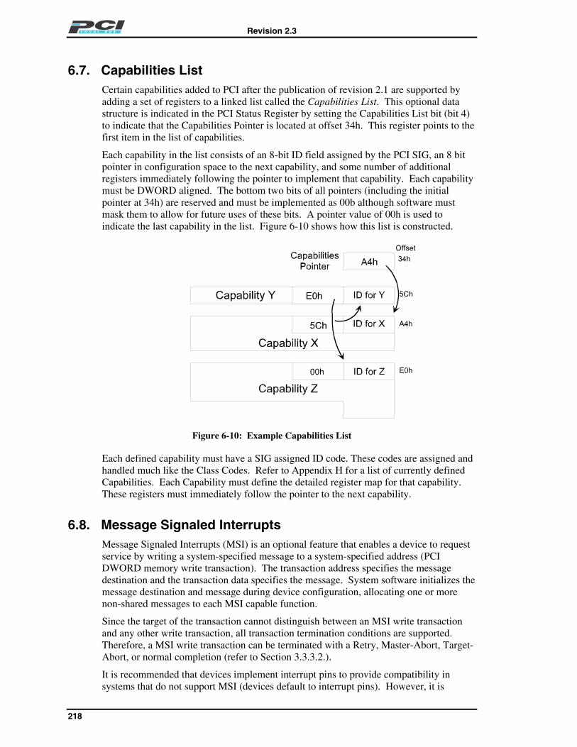
Revision 2.3
218
6.7. Capabilities ListCertain capabilities added to PCI after the publication of revision 2.1 are supported byadding a set of registers to a linked list called the Capabilities List. This optional datastructure is indicated in the PCI Status Register by setting the Capabilities List bit (bit 4)to indicate that the Capabilities Pointer is located at offset 34h. This register points to thefirst item in the list of capabilities.
Each capability in the list consists of an 8-bit ID field assigned by the PCI SIG, an 8 bitpointer in configuration space to the next capability, and some number of additionalregisters immediately following the pointer to implement that capability. Each capabilitymust be DWORD aligned. The bottom two bits of all pointers (including the initialpointer at 34h) are reserved and must be implemented as 00b although software mustmask them to allow for future uses of these bits. A pointer value of 00h is used toindicate the last capability in the list. Figure 6-10 shows how this list is constructed.
Figure 6-10: Example Capabilities List
Each defined capability must have a SIG assigned ID code. These codes are assigned andhandled much like the Class Codes. Refer to Appendix H for a list of currently definedCapabilities. Each Capability must define the detailed register map for that capability.These registers must immediately follow the pointer to the next capability.
6.8. Message Signaled InterruptsMessage Signaled Interrupts (MSI) is an optional feature that enables a device to requestservice by writing a system-specified message to a system-specified address (PCIDWORD memory write transaction). The transaction address specifies the messagedestination and the transaction data specifies the message. System software initializes themessage destination and message during device configuration, allocating one or morenon-shared messages to each MSI capable function.
Since the target of the transaction cannot distinguish between an MSI write transactionand any other write transaction, all transaction termination conditions are supported.Therefore, a MSI write transaction can be terminated with a Retry, Master-Abort, Target-Abort, or normal completion (refer to Section 3.3.3.2.).
It is recommended that devices implement interrupt pins to provide compatibility insystems that do not support MSI (devices default to interrupt pins). However, it is

Revision 2.3
219
expected that the need for interrupt pins will diminish over time. Devices that do notsupport interrupt pins due to pin constraints (rely on polling for device service) mayimplement messages to increase performance without adding additional pins. Therefore,system configuration software must not assume that a message capable device has aninterrupt pin.
Interrupt latency (the time from interrupt signaling to interrupt servicing) is systemdependent. Consistent with current interrupt architectures, message signaled interruptsdo not provide interrupt latency time guarantees.
6.8.1. Message Capability Structure
The capabilities mechanism (refer to Section 6.7.) is used to identify and configure a MSIcapable device. The message capability structure is illustrated in Figure 6-11. Eachdevice function that supports MSI (in a multi-function device) must implement its ownMSI capability structure. More then one MSI capability structure per function isprohibited.
Capability Pointer
Capability Pointer + 04h
Capability Pointer + 08h
31 16 15 8 7 0
Message Control Next Pointer Capability ID
Message Address
Message Data
Capability Pointer
Capability Pointer + 04h
Capability Pointer + 08h
Capability Pointer + 0Ch
31 16 15 8 7 0
Message Control Next Pointer Capability ID
Message Address
Message Data
Message Upper Address
Capability Structure for 32-bit Message Address
Capability Structure for 64-bit Message Address
Figure 6-11: Message Signaled Interrupt Capability Structure
To request service, an MSI function writes the contents of the Message Data register tothe address specified by the contents of the Message Address register (and, optionally,the Message Upper Address register for a 64-bit message address). A read of the addressspecified by the contents of the Message Address register produces undefined results.
The capability structure for a 32-bit message address (illustrated in Figure 6-11) isimplemented if the function supports a 32-bit message address. The capability structurefor a 64-bit message address (illustrated in Figure 6-11) is implemented if the functionsupports a 64-bit message address. If a device supports MSI and the device supports64-bit addressing (DAC) when acting as a master, the device is required to implement the64-bit message address structure.
The message control register indicates the function’s capabilities and provides systemsoftware control over MSI.
Each field is further described in the following sub-sections. Reserved registers and bitsalways return 0 when read and write operations have no effect. Read-only registersreturn valid data when read and write operations have no effect.

Revision 2.3
220
6.8.1.1. Capability ID
7::0 CAP_ID The value of 05h in this field identifies the function asmessage signaled interrupt capable. This field isread only.
6.8.1.2. Next Pointer
7::0 NXT_PTR Pointer to the next item in the capabilities list. Mustbe NULL for the final item in the list. This field is readonly.
6.8.1.3. Message Control
This register provides system software control over MSI. After reset, MSI is disabled (bit0 is cleared) and the function requests servicing via its INTx# pin (if supported). Systemsoftware can enable MSI by setting bit 0 of this register. System software is permitted tomodify the Message Control register’s read/write bits and fields. A device driver is notpermitted to modify the Message Control register’s read/write bits and fields.
Bits Field Description
15::08 ReservedAlways returns 0 on a read and a write operation hasno effect.
7 64 bit addresscapable
If 1, the function is capable of generating a 64-bitmessage address.
If 0, the function is not capable of generating a 64-bitmessage address.
This bit is read only.
Revision 2.3
221
Bits Field Description
6::4 Multiple MessageEnable
System software writes to this field to indicate thenumber of allocated messages (equal to or less thanthe number of requested messages). The number ofallocated messages is aligned to a power of two. If afunction requests four messages (indicated by aMultiple Message Capable encoding of “010”),system software can allocate either four, two, or onemessage by writing a “010”, “001, or “000” to thisfield, respectively. When MSI is enabled, a devicewill be allocated at least 1 message. The encoding isdefined as:
Encoding # of messages allocated
000 1
001 2
010 4
011 8
100 16
101 32
110 Reserved
111 Reserved
This field’s state after reset is “000”.
This field is read/write.
3::1 Multiple MessageCapable
System software reads this field to determine thenumber of requested messages. The number ofrequested messages must be aligned to a power oftwo (if a function requires three messages, itrequests four by initializing this field to “010”). Theencoding is defined as:
Encoding # of messages requested
000 1
001 2
010 4
011 8
100 16
101 32
110 Reserved
111 Reserved
This field is read/only.

Revision 2.3
222
Bits Field Description
0 MSI EnableIf 1, the function is permitted to use MSI to requestservice and is prohibited from using its INTx# pin (ifimplemented). System configuration software setsthis bit to enable MSI. A device driver is prohibitedfrom writing this bit to mask a function’s servicerequest. Refer to Section 6.2.2. for control of INTx#.
If 0, the function is prohibited from using MSI torequest service.
This bit’s state after reset is 0 (MSI is disabled).
This bit is read/write.
6.8.1.4. Message Address
Bits Field Description
31::02 MessageAddress
System-specified message address.
If the Message Enable bit (bit 0 of the MessageControl register) is set, the contents of this registerspecify the DWORD aligned address (AD[31::02]) forthe MSI memory write transaction. AD[1::0] aredriven to zero during the address phase.
This field is read/write.
01::00 Reserved Always returns 0 on read. Write operations have noeffect.
6.8.1.5. Message Upper Address (Optional)
Bits Field Description
31::00 Message UpperAddress
System-specified message upper address.
This register is optional and is implemented only ifthe device supports a 64-bit message address (bit 7in Message Control register set)49. If the MessageEnable bit (bit 0 of the Message Control register) isset, the contents of this register (if non-zero) specifythe upper 32-bits of a 64-bit message address(AD[63::32]). If the contents of this register are zero,the device uses the 32 bit address specified by themessage address register.
This field is read/write.
49 This register is required when the device supports 64-bit addressing (DAC) when acting as a master.

Revision 2.3
223
6.8.1.6. Message Data
Bits Field Description
15::00 Message Data System-specified message.
Each MSI function is allocated up to 32 uniquemessages.
System architecture specifies the number of uniquemessages supported by the system.
If the Message Enable bit (bit 0 of the MessageControl register) is set, the message data is drivenonto the lower word (AD[15::00]) of the memorywrite transaction’s data phase. AD[31::16] aredriven to zero during the memory write transaction’sdata phase. C/BE[3::0]# are asserted during thedata phase of the memory write transaction.
The Multiple Message Enable field (bits 6-4 of theMessage Control register) defines the number of loworder message data bits the function is permitted tomodify to generate its system software allocatedmessages. For example, a Multiple Message Enableencoding of “010” indicates the function has beenallocated four messages and is permitted to modifymessage data bits 1 and 0 (a function modifies thelower message data bits to generate the allocatednumber of messages). If the Multiple MessageEnable field is “000”, the function is not permitted tomodify the message data.
This field is read/write.
6.8.2. MSI Operation
At configuration time, system software traverses the function’s capability list. If acapability ID of 05h is found, the function implements MSI. System software reads theMSI capability structure’s Message Control register to determine the function’scapabilities.
System software reads the Multiple Message Capable field (bits 3-1 of the MessageControl register) to determine the number of requested messages. System software writesto the Multiple Message Enable field (bits 6-4 of the Message Control register) to allocateeither all or a subset of the requested messages. For example, a function can request fourmessages and be allocated either four, two, or one message. The number of messagesrequested and allocated are aligned to a power of two (a function that requires threemessages must request four).
If the 64-bit Address Capable bit (bit 7 of the Message Control register) is set, systemsoftware initializes the MSI capability structure’s Message Address register (specifyingthe lower 32 bits of the message address) and the Message Upper Address register(specifying the upper 32 bits of the message address) with a system-specified messagedestination address. System software may program the Message Upper Address registerto zero so that the function generates a 32-bit address for the MSI write transaction. Ifthis bit is clear, system software initializes the MSI capability structure’s Message

Revision 2.3
224
Address register (specifying a 32-bit message address) with a system specified messagedestination address.
System software initializes the MSI capability structure’s Message Data register with asystem specified message. Care must be taken to initialize only the Message Dataregister (i.e., a 2-byte value) and not modify the upper two bytes of that DWORDlocation.
To maintain backward compatibility, the MSI Enable bit (bit 0 of the Message Controlregister) is cleared after reset (MSI is disabled). System configuration software sets thisbit to enable MSI. A device driver is prohibited from writing this bit to mask a function’sservice request. Once enabled, a function is prohibited from using its INTx# pin (ifimplemented) to request service (MSI and INTx# are mutually exclusive).
Once MSI is enabled (bit 0 of the Message Control Register is set), the function may sendmessages. To send a message, a function does a DWORD memory write to the addressspecified by the contents of the Message Address register (and optionally the MessageUpper Address register for a 64-bit message address). The DWORD that is written ismade up of the value in the Message Data register in the lower two bytes and zeroes inthe upper two bytes. If the Multiple Message Enable field (bits 6-4 of the MessageControl register) is non-zero, the device is permitted to modify the low order bits of themessage data to generate multiple messages. For example, a Multiple Message Enableencoding of “010” indicates the function is permitted to modify message data bits 1 and 0to generate up to four unique messages. If the Multiple Message Enable field is “000”,the function is not permitted to modify the message data. How a function uses multiplemessages (when allocated) is device dependent. A function must handle being allocatedless messages than requested.
If a device signals the same message many times, only one message is guaranteed to beserviced. If all messages must be serviced, a device driver handshake is required. Inother words, once a function signals Message A, it cannot signal Message A again until itis explicitly enabled to do so by its device driver (provided all messages must beserviced). If some messages can be lost, a device driver handshake is not required. Forfunctions that support multiple messages, a function can signal multiple unique messagesand is guaranteed that each unique message will be serviced. For example, a device cansignal Message A followed by Message B without any device driver handshake (bothMessage A and Message B will be serviced).
An MSI is by definition a non-shared interrupt that enforces data consistency (ensures theinterrupt service routine accesses the most recent data). The system guarantees that anydata written by the device prior to sending the MSI has reached its final destinationbefore the interrupt service routine accesses that data. Therefore, a device driver is notrequired to read its device before servicing its MSI.

Revision 2.3
225
6.8.2.1. MSI Transaction Termination
The target of an MSI transaction cannot distinguish between it and any other memorywrite transaction. The termination requirements for an MSI transaction are the same asfor any other memory write transaction except as noted below.
If the MSI write transaction is terminated with a Master-Abort or a Target-Abort, themaster that originated the MSI memory write transaction is required to report the error byasserting SERR# (if bit 8 in the Command register is set) and to set the appropriate bitsin the Status register (refer to Section 3.7.4.2.). An MSI memorywrite transaction isignored by the target if it is terminated with a Master-Abort or Target-Abort.
Refer to the PCI-to-PCI Bridge Architecture Specification, Revision 1.1 (Section 6, ErrorSupport) for PCI-to-PCI bridge SERR# generation in response to error conditions fromposted memory writes on the destination bus.
Note that SERR# generation in an MSI-enabled environment containing PCI-to-PCIbridges requires the SERR# reporting enable bits in all devices in the MSI message pathto be set. For PCI-to-PCI bridges specifically, refer to Section 6.2.2 and PCI-to-PCIBridge Architecture Specification, Revision 1.1, Sections 3.2.4.3 and 3.2.5.17.).
If the MSI write transaction results in a data parity error, the master that originated theMSI write transaction is required to assert SERR# (if bit 8 in the Command register isset) and to set the appropriated bits in the Status register (refer to Section 3.7.4.).
6.8.2.2. MSI Transaction Reception and Ordering Requirements
As with all memory write transactions, the device that includes the target of the interruptmessage (the interrupt receiver) is required to complete all interrupt message transactionsas a target without requiring other transactions to complete first as a master. (Refer toSection 3.3.3.3.4. In general, this means that the message receiver must complete theinterrupt message transaction independent of when the CPU services the interrupt. Forexample, each time the interrupt receiver receives an interrupt message, it could set a bitin an internal register indicating that this message had been received and then completethe transaction on the bus. The appropriate interrupt service routine would later bedispatched because this bit was set. The message receiver would not be allowed to delaythe completion of the interrupt message on the bus pending acknowledgement from theprocessor that the interrupt was being serviced. Such dependencies can lead to deadlockwhen multiple devices generate interrupt messages simultaneously.
Although interrupt messages remain strictly ordered throughout the PCI bus hierarchy,the order of receipt of the interrupt messages does not guarantee any order in which theinterrupts will be serviced. Since the message receiver must complete all interruptmessage transactions without regard to when the interrupt was actually serviced, themessage receiver will generally not maintain any information about the order in whichthe interrupts were received. This is true both of interrupt messages received fromdifferent devices, and multiple messages received from the same device. If a devicerequires one interrupt message to be serviced before another, then the device must notsend the second interrupt message until the first one has been serviced.

Revision 2.3
226

Revision 2.3
227
Chapter 766 MHz PCI Specification
7.1. IntroductionThe 66 MHz PCI bus is a compatible superset of PCI defined to operate up to amaximum clock speed of 66 MHz. The 66 MHz PCI bus is intended to be used by lowlatency, high bandwidth bridges, and peripherals. Systems may augment the 66 MHzPCI bus with a separate 33 MHz PCI bus to handle lower speed peripherals.
Differences between 33 MHz PCI and 66 MHz PCI are minimal. Both share the sameprotocol, signal definitions, and connector layout. To identify 66 MHz PCI devices, onestatic signal is added by redefining an existing ground pin, and one bit is added to theConfiguration Status register. Bus drivers for the 66 MHz PCI bus meet the same DCcharacteristics and AC drive point limits as 33 MHz PCI bus drivers; however, 66 MHzPCI requires faster timing parameters and redefined measurement conditions. As a result,66 MHz PCI buses may support smaller loading and trace lengths.
A 66 MHz PCI device operates as a 33 MHz PCI device when it is connected to a33 MHz PCI bus. Similarly, if any 33 MHz PCI devices are connected to a 66 MHz PCIbus, the 66 MHz PCI bus will operate as a 33 MHz PCI bus.
The programming models for 66 MHz PCI and 33 MHz PCI are the same, includingconfiguration headers and class types. Agents and bridges include a 66 MHz PCI statusbit.
7.2. ScopeThis chapter defines aspects of 66 MHz PCI that differ from those defined elsewhere inthis document, including information on device and bridge support. This chapter will notrepeat information defined elsewhere.

Revision 2.3
228
7.3. Device Implementation Considerations
7.3.1. Configuration Space
Identification of a 66 MHz PCI-compliant device is accomplished through the use of theread-only 66MHZ_CAPABLE flag located in bit 5 of the PCI Status register (seeFigure 6-3). If set, this bit signifies that the device is capable of operating in 66 MHzmode.
7.4. Agent ArchitectureA 66 MHz PCI agent is defined as a PCI agent capable of supporting 66 MHz PCI.
All 66 MHz PCI agents must support a read-only 66MHZ_CAPABLE flag located inbit 5 of the PCI Status register for that agent. If set, the 66MHZ_CAPABLE bit signifiesthat the agent can operate in 66 MHz PCI mode.50
7.5. Protocol
7.5.1. 66MHZ_ENABLE (M66EN) Pin Definition
Pin 49B on the PCI connector is designated M66EN. Add-in cards and bus segments notcapable of operation in 66 MHz mode must connect this pin to ground. A 66 MHz PCIsystem board segment must provide a single pullup resistor to Vcc on the M66EN pin.
Refer to Section 7.7.7. for the appropriate pullup value. M66EN is bused to all 66 MHzPCI connectors and system board-only 66 MHz PCI components that include the M66ENpin. The 66 MHz PCI clock generation circuitry must connect to M66EN to generate theappropriate clock for the segment (33 to 66 MHz if M66EN is asserted, 0 to 33 MHz ifM66EN is deasserted).
If a 66 MHz PCI agent requires clock speed information (for example, for a PLL bypass),it is permitted to use M66EN as an input. If a 66 MHz PCI agent can run without anyknowledge of the speed, it is permitted to leave M66EN disconnected.
50 Configuration software identifies agent capabilities by checking the 66MHZ_CAPABLE bit in theStatus register. This includes both the primary and secondary Status registers in a PCI-to-PCI bridge. Thisallows configuration software to detect a 33 MHz PCI agent on a 66 MHz PCI bus or a 66 MHz PCI agenton a 33 MHz PCI bus and issue a warning to the user describing the situation.

Revision 2.3
229
Table 7-1: Bus and Agent Combinations
Bus66MHZ_CAPABLE51
Agent66MHZ_CAPABLE Description
0 0 33 MHz PCI agent located on a33 MHz PCI bus
0 1 66 MHz PCI agent located on a33 MHz PCI bus52
1 0 33 MHz PCI agent located on a66 MHz PCI bus52
1 1 66 MHz PCI agent located on a66 MHz PCI bus
7.5.2. Latency
The 66 MHz PCI bus is intended for low latency devices. It is required that the targetinitial latency not exceed 16 clocks.
7.6. Electrical Specification
7.6.1. Overview
This chapter defines the electrical characteristics and constraints of 66 MHz PCIcomponents, systems, and add-in cards, including connector pin assignments.
All electrical specifications from Chapter 4 of this document apply to 66 MHz PCI exceptwhere explicitly superseded. Specifically:
• The 66 MHz PCI bus uses the 3.3V signaling environment.
• Timing parameters have been scaled to 66 MHz.
• AC test loading conditions have been changed.
51 The bus 66MHZ_CAPABLE status bit is located in a bridge’s Status registers.
52 This condition may cause the configuration software to generate a warning to the user stating that theadd-in card is installed in an inappropriate socket and should be relocated.

Revision 2.3
230
7.6.2. Transition Roadmap to 66 MHz PCI
The 66 MHz PCI bus utilizes the PCI bus protocol; 66 MHz PCI simply has a highermaximum bus clock frequency. Both 66 MHz and 33 MHz devices can coexist on thesame bus segment. In this case, the bus segment will operate as a 33 MHz segment.
To ensure compatibility, 66 MHz PCI devices have the same DC specifications and ACdrive point limits as 33 MHz PCI devices. However, 66 MHz PCI requires modifiedtiming parameters as described in the analysis of the timing budget shown in Figure 7-1.
Tcyc ≥ Tval + Tprop + Tskew + Tsu
Tval =11 ns Tprop = 10 ns Tskew = 2ns Tsu=7ns
Tval Tprop Tskew Tsu6 ns 5 ns 1 ns 3 ns
Tcyc = 30 ns
Tcyc = 15 ns
33 MHZ
66 MHZ
Figure 7-1: 33 MHz PCI vs. 66 MHz PCI Timing
Since AC drive requirements are the same for 66 MHz PCI and 33 MHz PCI, it isexpected that 66 MHz PCI devices will function on 33 MHz PCI buses. Therefore,66 MHz PCI devices must meet both 66 MHz PCI and 33 MHz PCI requirements.
7.6.3. Signaling Environment
A 66 MHz PCI system board segment must use the PCI 3.3V keyed connector.Therefore, 66 MHz PCI system board segments accept either 3.3V or Universal add-incards; 5V add-in cards are not supported.
While 33 MHz PCI bus drivers are defined by their V/I curves, 66 MHz PCI outputbuffers are specified in terms of their AC and DC drive points, timing parameters, andslew rate. The minimum AC drive point defines an acceptable first step voltage and mustbe reached within the maximum Tval time. The maximum AC drive point limits theamount of overshoot and undershoot in the system. The DC drive point specifies steadystate conditions. The minimum slew rate and the timing parameters guarantee 66 MHzoperation. The maximum slew rate minimizes system noise. This method ofspecification provides a more concise definition for the output buffer.

Revision 2.3
231
7.6.3.1. DC Specifications
Refer to Section 4.2.2.1.
7.6.3.2. AC Specifications
Table 7-2: AC Specifications
Symbol Parameter Condition Min Max Units Notes
AC Drive Points
Ioh(AC,min) Switching CurrentHigh, minimum
Vout = 0.3Vcc -12Vcc - mA 1
Ioh(AC,max) Switching CurrentHigh, maximum
Vout = 0.7Vcc - -32Vcc mA
Iol(AC,min) Switching CurrentLow, minimum
Vout = 0.6Vcc 16Vcc - mA 1
Iol(AC,max) SwitchingCurrent Low,maximum
Vout = 0.18Vcc - 38Vcc mA
DC Drive Points
VOH Output highvoltage
Iout = -0.5 mA 0.9Vcc - V 2
VOL Output lowvoltage
Iout = 1.5 mA - 0.1Vcc V 2
Slew Rate
tr Output rise slewrate
0.3Vcc to 0.6Vcc 1 4 V/ns 3
tf Output fall slewrate
0.6Vcc to 0.3Vcc 1 4 V/ns 3
Clamp Current
Ich High clampcurrent
Vcc + 4 > Vin ≥ Vcc + 1 25 + (Vin - Vcc - 1) / 0.015 - mA
Icl Low clampcurrent
-3 < Vin ≤ -1 -25 + (Vin + 1) / 0.015 - mA
NOTES:1. Switching current characteristics for REQ# and GNT# are permitted to be one half of that specified here; i.e., half
size drivers may be used on these signals. This specification does not apply to CLK and RST# which are systemoutputs. "Switching Current High" specifications are not relevant to SERR#, PME#, INTA#, INTB#, INTC#, andINTD# which are open drain outputs.
2. These DC values are duplicated from Section 4.2.2.1. and are included here for completeness.
3. This parameter is to be interpreted as the cumulative edge rate across the specified range rather than theinstantaneous rate at any point within the transition range. The specified load (see Figure 7-7) is optional. Thedesigner may elect to meet this parameter with an unloaded output . However, adherence to both maximum andminimum parameters is required (the maximum is not simply a guideline). Rise slew rate does not apply to opendrain outputs.
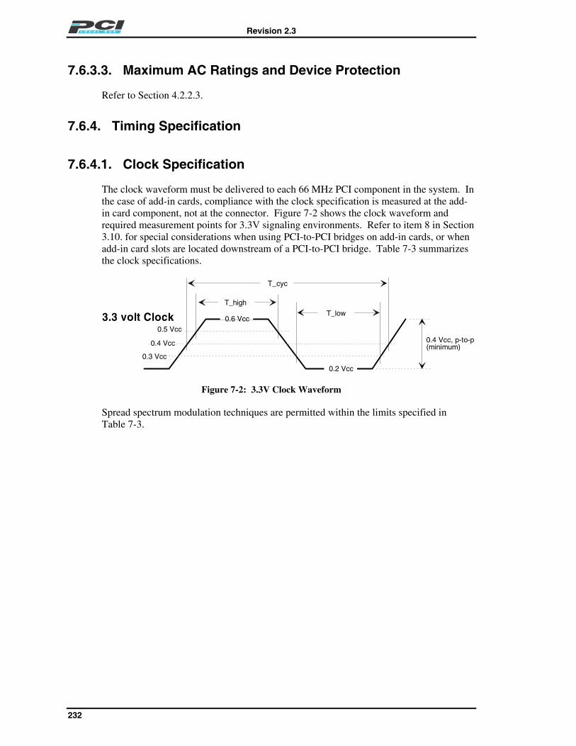
Revision 2.3
232
7.6.3.3. Maximum AC Ratings and Device Protection
Refer to Section 4.2.2.3.
7.6.4. Timing Specification
7.6.4.1. Clock Specification
The clock waveform must be delivered to each 66 MHz PCI component in the system. Inthe case of add-in cards, compliance with the clock specification is measured at the add-in card component, not at the connector. Figure 7-2 shows the clock waveform andrequired measurement points for 3.3V signaling environments. Refer to item 8 in Section3.10. for special considerations when using PCI-to-PCI bridges on add-in cards, or whenadd-in card slots are located downstream of a PCI-to-PCI bridge. Table 7-3 summarizesthe clock specifications.
T_high
T_low
0.3 Vcc
T_cyc
0.5 Vcc
3.3 volt Clock
0.4 Vcc
0.6 Vcc
0.2 Vcc
0.4 Vcc, p-to-p(minimum)
Figure 7-2: 3.3V Clock Waveform
Spread spectrum modulation techniques are permitted within the limits specified inTable 7-3.

Revision 2.3
233
Table 7-3: Clock Specifications
66 MHz 33 MHz4
Symbol Parameter Min Max Min Max Units Notes
Tcyc CLK Cycle Time 15 30 30 ∞ ns 1,3
Thigh CLK High Time 6 11 ns
Tlow CLK Low Time 6 11 ns
- CLK Slew Rate 1.5 4 1 4 V/ns 2
Spread Spectrum Requirements
fmod modulationfrequency
30 33 - - kHz
fspread frequencyspread
-1 0 %
NOTES:
1. In general, all 66 MHz PCI components must work with any clock frequency up to 66 MHz. CLKrequirements vary depending upon whether the clock frequency is above 33 MHz.
a. Device operational parameters at frequencies at or under 33 MHz will conform to the specifications inChapter 4. The clock frequency may be changed at any time during the operation of the system solong as the clock edges remain "clean" (monotonic) and the minimum cycle and high and low timesare not violated. The clock may only be stopped in a low state. A variance on this specification isallowed for components designed for use on the system board only. Refer to Section 4.2.3.1. formore information.
b. For clock frequencies between 33 MHz and 66 MHz, the clock frequency may not change exceptwhile RST# is asserted or when spread spectrum clocking (SSC) is used to reduce EMI emissions.
2. Rise and fall times are specified in terms of the edge rate measured in V/ns. This slew rate must be metacross the minimum peak-to-peak portion of the clock waveform as shown in Figure 7-2. Clock slew rateis measured by the slew rate circuit shown in Figure 7-7.
3. The minimum clock period must not be violated for any single clock cycle; i.e., accounting for all systemjitter.
4. These values are duplicated from Section 4.2.3.1. and included here for comparison.
Implementation Note: Spread Spectrum Clocking (SSC)Spreading the frequency is only allowed below the maximum clock frequency that isspecified (i.e., the minimum clock period shown in Table 7-3 cannot be violated). Inother words, the frequency change can only occur to reduce the frequency of the clockand never to increase it. When PLLs are used to track CLK, they need to track the SSCmodulation quickly in order not to accumulate excessive phase difference between thePLL input and output clocks (commonly referred to as SSC tracking skew). The amountof tracking skew depends on the PLL bandwidth, phase angle at 30-33 kHz, and theamount of the spread. It is desirable to maximize bandwidth and/or reduce the phaseangle in order to minimize the tracking skew; otherwise, the SSC frequency spread of thesystem must be reduced, thereby, reducing the SSC EMI reduction capability.

Revision 2.3
234
7.6.4.2. Timing Parameters
Table 7-4: 66 MHz and 33 MHz Timing Parameters
66 MHz 33 MHz7
Symbol Parameter Min Max Min Max Units Notes
Tval CLK to Signal Valid Delay -bused signals
2 6 2 11 ns 1, 2,3, 8
Tval(ptp) CLK to Signal Valid Delay -point to point signals
2 6 2 12 ns 1, 2,3, 8
Ton Float to Active Delay 2 2 ns 1, 8, 9
Toff Active to Float Delay 14 28 ns 1, 9
Tsu Input Setup Time to CLK -bused signals
3 7 ns 3, 4,10
Tsu(ptp) Input Setup Time to CLK -point to point signals
5 10,12 ns 3, 4
Th Input Hold Time from CLK 0 0 ns 4
Trst Reset Active Time afterpower stable
1 1 ms 5
Trst-clk Reset Active Time after CLKstable
100 100 µs 5
Trst-off Reset Active to output floatdelay
40 40 ns 5, 6
trrsu REQ64# to RST# setup time 10Tcyc 10Tcyc ns
trrh RST# to REQ64# hold time 0 50 0 50 ns
Trhfa RST# high to firstConfiguration access
225 225 clocks
Trhff RST# high to first FRAME#assertion
5 5 clocks
NOTES:
1. See the timing measurement conditions in Figure 7-3. It is important that all driven signal transitions drive to theirVoh or Vol level within one Tcyc.
2. Minimum times are measured at the package pin with the load circuit shown in Figure 7-7. Maximum times aremeasured with the load circuit shown in Figures 7-5 and 7-6.
3. REQ# and GNT# are point-to-point signals and have different input setup times than do bused signals. GNT# andREQ# have a setup of 5 ns at 66 MHz. All other signals are bused.
4. See the timing measurement conditions in Figure 7-4.
5. If M66EN is asserted, CLK is stable when it meets the requirements in Section 7.6.4.1. RST# is asserted anddeasserted asynchronously with respect to CLK. Refer to Section 4.3.2. for more information.
6. All output drivers must be floated when RST# is active. Refer to Section 4.3.2. for more information.
7. These values are duplicated from Section 4.2.3.2. and are included here for comparison.

Revision 2.3
235
8. When M66EN is asserted, the minimum specification for Tval(min), Tval(ptp)(min), and Ton may be reduced to
1 ns if a mechanism is provided to guarantee a minimum value of 2 ns when M66EN is deasserted.
9. For purposes of Active/Float timing measurements, the Hi-Z or “off” state is defined to be when the total currentdelivered through the component pin is less than or equal to the leakage current specification.
10. Setup time applies only when the device is not driving the pin. Devices cannot drive and receive signals at thesame time. Refer to Section 3.10., item 9 for additional details.
7.6.4.3. Measurement and Test Conditions
CLK
OUTPUTDELAY
T_val
V_test
V_tfall
V_th
V_tl
T_on
Tri-StateOUTPUT
OUTPUTDELAY
V_trise
T_val
T_off
Figure 7-3: Output Timing Measurement Conditions
INPUTinputsvalid
V_th
V_tl
T_hT_su
CLK
V_test
V_test
V_test V_max
V_th
V_tl
Figure 7-4: Input Timing Measurement Conditions

Revision 2.3
236
Table 7-5: Measurement Condition Parameters
Symbol 3.3V Signaling Units NotesVth 0.6Vcc V 1
Vtl 0.2Vcc V 1
Vtest 0.4Vcc V
Vtrise 0.285Vcc V 2
Vtfall 0.615Vcc V 2
Vmax 0.4Vcc V 1
Input SignalSlew Rate
1.5 V/ns 3
NOTES:
1. The test for the 3.3V environment is done with 0.1*Vcc of overdrive.Vmax specifies the maximum peak-to-peak waveform allowed formeasuring input timing. Production testing may use different voltagevalues but must correlate results back to these parameters.
2. Vtrise and Vtfall are reference voltages for timing measurements only.Developers of 66 MHz PCI systems need to design buffers that launchenough energy into a 25 Ω transmission line so that correct input levelsare guaranteed after the first reflection.
3. Outputs will be characterized and measured at the package pin withthe load shown in Figure 7-7. Input signal slew rate will be measuredbetween 0.2Vcc and 0.6Vcc.
25 Ω 10 pF
1/2 in. max.
outputbuffer
pin
Figure 7-5: Tval(max) Rising Edge
25 Ω10 pF
Vcc
1/2 in. max.
Figure 7-6: Tval(max) Falling Edge

Revision 2.3
237
1K Ω10 pF
outputbuffer
pin 1/2 in. max.
Vcc
1K Ω
Figure 7-7: Tval (min) and Slew Rate
7.6.5. Vendor Provided Specification
Refer to Section 4.2.5.
7.6.6. Recommendations
7.6.6.1. Pinout Recommendations
Refer to Section 4.2.6.
The 66 MHz PCI electrical specification and physical requirements must be met;however, the designer is permitted to modify the suggested pinout shown in Figure 4-9 asrequired.
7.6.6.2. Clocking Recommendations
This section describes a recommended method for routing the 66 MHz PCI clock signal.Routing the 66 MHz PCI clock as a point-to-point signal from individual low-skew clockdrivers to both system board and add-in card components will greatly reduce signalreflection effects and optimize clock signal integrity. This, in addition to observing thephysical requirements outlined in Section 4.4.3.1., will minimize clock skew.
Developers must pay careful attention to the clock trace length limits stated inSection 4.4.3.1. and the velocity limits in Section 4.4.3.3. Figure 7-8 illustrates therecommended method for routing the 66 MHz PCI clock signal.

Revision 2.3
238
Clock Source Add-in Card
PCI Add-inConnector
66 MHzDevice C
66 MHzDevice B
66 MHzDevice A
Figure 7-8: Recommended Clock Routing
7.7. System Board Specification
7.7.1. Clock Uncertainty
The maximum allowable clock skew including jitter is 1 ns. This specification appliesnot only at a single threshold point, but at all points on the clock edge that fall in theswitching range defined in Table 7-6 and Figure 7-9. The maximum skew is measuredbetween any two components,53 not between connectors. To correctly evaluate clockskew, the system designer must take into account clock distribution on the add-in card asspecified in Section 4.4.
Developers must pay careful attention to the clock trace length limits stated inSection 4.4.3.1. and the velocity limits in Section 4.4.3.3.
Table 7-6: Clock Skew Parameters
Symbol 66 MHz 3.3V Signaling 33 MHz 3.3V Signaling Units
Vtest 0.4Vcc 0.4Vcc V
Tskew 1 (max) 2 (max) ns
53 The system designer must address an additional source of clock skew. This clock skew occurs betweentwo components that have clock input trip points at opposite ends of the Vil - Vih range. In certaincircumstances, this can add to the clock skew measurement as described here. In all cases, total clockskew must be limited to the specified number.

Revision 2.3
239
CLK(@Device #1)
CLK(@Device #2)
V_testV_ih
T_skew
T_skew
T_skew
V_testV_il
V_il
V_ih
Figure 7-9: Clock Skew Diagram
7.7.2. Reset
Refer to Section 4.3.2.
7.7.3. Pullups
The 66 MHz PCI bus requires a single pullup resistor, supplied by the system board, onthe M66EN pin. Refer to Section 7.7.7. for the resistor value.
7.7.4. Power
7.7.4.1. Power Requirements
Refer to Section 4.3.4.1.
7.7.4.2. Sequencing
Refer to Section 4.3.4.2.
7.7.4.3. Decoupling
Refer to Section 4.3.4.3.
7.7.5. System Timing Budget
Refer to Section 4.3.5.
The total clock period can be divided into four segments. Valid output delay (Tval) andinput setup times (Tsu) are specified by the component specification. Total clock skew(Tskew) and bus propagation times (Tprop) are system parameters. Tprop is a systemparameter that is indirectly specified by subtracting the other timing budget componentsfrom the cycle time. Table 7-7 lists timing budgets for several bus frequencies.

Revision 2.3
240
Table 7-7: Timing Budgets
Timing Element 33 MHz 66 MHz 50 MHz1 Units Notes
Tcyc 30 15 20 ns
Tval 11 6 6 ns
Tprop 10 5 10 ns 2
Tsu 7 3 3 ns
Tskew 2 1 1 ns 3
NOTES:
1. The 50 MHz example is shown for example purposes only.
2. These times are computed. The other times are fixed. Thus, slowing down the bus clock enables thesystem manufacturer to gain additional distance or add additional loads. The component specificationsare required to guarantee operation at 66 MHz.
3. Clock skew specified here includes all sources of skew. If spread spectrum clocking (SSC) is used on thesystem board, the maximum clock skew at the input of the device on an add-in card includes SSC trackingskew.
7.7.6. Physical Requirements
7.7.6.1. Routing and Layout Recommendations for Four-LayerSystem Boards
Refer to Section 4.3.6.1.
7.7.6.2. System Board Impedance
Refer to Section 4.3.6.2. Timing numbers are changed according to the tables in thischapter.
7.7.7. Connector Pin Assignments
The M66EN pin (pin 49B) is the only connector difference between bus segmentscapable of 66 MHz operation and those limited to 33 MHz. Refer to Section 4.3.7. forsystem board connectors. This pin is a normal ground pin in implementations that are notcapable of 66 MHz operation.
In implementations that are 66-MHz-capable, the M66EN pin is bused between allconnectors54 within the single logical bus segment that is 66-MHz-capable, and this net ispulled up with a 5 kΩ resistor to Vcc. Also, this net is connected to the M66EN input
54 As a general rule, there will be only one such connector, but more than one are possible in certain cases.

Revision 2.3
241
pin of components located on the same logical bus segment of the system board. Thissignal is static; there is no stub length restriction.
To complete an AC return path, a 0.01 µF capacitor must be located within 0.25 inches ofthe M66EN pin, of each such add-in card connector and must decouple the M66ENsignal to ground. Any attached component or installed add-in card that is not 66-MHz-capable, must pull the M66EN net to the Vil input level. The remaining components,add-in cards, and the logical bus segment clock resource are, thereby, signaled to operatein 33-MHz mode.
7.8. Add-in Card SpecificationsThe 66 MHz add-in card specifications are the same as the 33 MHz add-in cardspecifications (refer to Section 4.4) except as noted in this section. The M66EN pin(pin 49B) is the only connector difference between add-in cards capable of 66 MHzoperation and those limited to 33 MHz. Refer to Section 4.4.1. for the add-in card edge-connector. The M66EN pin is a normal ground pin in implementations that are notcapable of 66 MHz operation.
In implementations that are 66-MHz-capable, the M66EN pin must be decoupled toground with a 0.01 µF capacitor, which must be located within 0.25 inches of the edgecontact to complete an AC return path. If the M66EN pin is pulled to the Vil input level,it indicates that the add-in card must operate in the 33-MHz mode.

Revision 2.3
242

Revision 2.3
243
Chapter 8System Support for SMBus
The SMBus interface is based upon the System Management Bus Specification55
(SMBus 2.0 Specification). This two-wire serial interface has low power and lowsoftware overhead characteristics that make it well suited for low-bandwidth systemmanagement functions. The capabilities enabled by the SMBus interface include, but arenot limited to, the following:
• Support for client management technologies
• Support for server management technologies
• Support for thermal sensors and other instrumentation devices on add-in cards
• Add-in card identification when the bus is in the B3 state or when the PCI device isin the D3hot or D3cold states as defined in the PCI Power Management InterfaceSpecification56
8.1. SMBus System RequirementsSMBus device interfaces must meet the electrical and protocol requirements in theSMBus 2.0 Specification.
The SMBus interface connections on the PCI connector are optional. However, if theSMBus interface is supported, then all of the following requirements must be met.
8.1.1. Power
It is recommended that the system board provide 3.3V auxiliary power to the PCIconnector (pin 14A). This allows an add-in card to maintain SMBus functionality whenthe system is in a low power state.
55 System Management Bus (SMBus) Specification, Version 2.0, available from the SMBus website athttp://www.smbus.org.
56 PCI Bus Power Management Interface Specification, Rev. 1.1 available from the PCI Special InterestGroup website at http://www.pcisig.com.

Revision 2.3
244
8.1.2. Physical and Logical SMBus
A physical SMBus segment is defined as a set of SMBus device interfaces whoseSMBCLK and SMBDAT lines are directly connected to one another (i.e., not connectedthrough an SMBus repeater or bridge). Each physical bus segment must meet theelectrical requirements of the SMBus 2.0 Specification.
A logical SMBus is defined as one or more physical SMBuses having a single SMBusaddress space and a single SMBus arbitration domain. Multiple physical SMBussegments are connected into a single logical SMBus segment by means of bus repeaters.An SMBus address space is a logical connection of SMBus devices such that two deviceswith the same slave address will conflict with one another. An arbitration domain is acollection of one or more physical buses connected such that bus signal assertions causedby any device on any physical bus within the arbitration domain are seen by all deviceson all the physical buses within the arbitration domain.
8.1.3. Bus Connectivity
Connection of SMBus to system board add-in card slot connectors is optional. However,if SMBus is connected to one slot in a chassis, it must be connected to all slots in thatchassis. SMBus-connected slots in a chassis must be in the same logical SMBus. Thislogical SMBus may optionally be broken during system initialization or hot remove toallow the system to determine which SMBus device is in which PCI slot, but must berestored before the end of system initialization and during normal operation.
A typical implementation of a single physical SMBus is illustrated in Figure 8-1. TheSMBus host bus controller is provided by the system.
SMBCLK
SMBDAT SMBCLK
SMBDAT
3.3Vaux 3.3Vaux
Add-in Card #0
Host BusController
PCIHost Add-in Cards
SMBCLK
SMBDAT
SMBCLK
SMBDAT
Add-in Card #1
Add-in Card #n-1
Figure 8-1. A Typical Single Physical SMBus

Revision 2.3
245
An SMBus in any one chassis is not required to support connection to an SMBus inanother chassis. This does not preclude connection to another chassis, but thespecification of any such connection is outside the scope of this document.
System board configurations with one or more SMBus-connected PCI bus segments mustcontain a single logical SMBus between all the PCI bus segments. There is nocorrelation between PCI bus segments and SMBus physical buses. As such, the SMBusis wired “around” a PCI bus bridge and not “through” it.
8.1.4 Master and Slave Support
As defined in the SMBus 2.0 Specification, an SMBus transaction occurs between amaster and a slave. A master is a device that issues commands, generates the clocksignal, and terminates the bus transaction. A slave is a device that receives or responds tothe bus transaction.
The system board supporting the SMBus interface must have both slave and mastercapability and support the multi-master arbitration mechanism as defined in the SMBus2.0 Specification.
8.1.5 Addressing and Configuration
An address resolution protocol (ARP) is defined in the SMBus 2.0 Specification that isused to assign slave addresses to SMBus devices. Although optional in the SMBus 2.0Specification, it is required that systems that connect the SMBus to PCI slots implementthe ARP for assignment of SMBus slave addresses to SMBus interface devices on PCIadd-in cards. The system must execute the ARP on a logical SMBus whenever any PCIbus segment associated with the logical SMBus exits the B3 state or a device in anindividual slot associated with the logical SMBus exits the D3cold state. Prior toexecuting the ARP, the system must insure that all ARP-capable SMBus interface devicesare returned to their default address state57.
The system may optionally support in a chassis inclusion of a single add-in card with anSMBus interface device with a fixed address in the range C6h – C9h. Such a systemmust not contain SMBus interface devices with a fixed address in this range and must notassign addresses in this range to other SMBus interface devices on PCI add-in cards.Such systems are not required to provide mechanisms to resolve conflicts if more thanone such add-in card is installed.
57 The System Management Bus (SMBus) Specification, Version 2.0 allows SMBus devices that are notassociated with PCI add-in cards to have fixed SMBus addresses that are not assigned by the ARP. Suchdevices include, for example, system board temperature sensors. The SMBus slave addresses of suchdevices must be known to the system prior to the execution of the ARP and are not assigned to any ARP-capable SMBus devices.

Revision 2.3
246
Implementation Note: Fixed Address SMBus Interface Devices on anAdd-in CardVersions of the SMBus Specification prior to 2.0 did not include the ARP and SMBusinterface devices compliant with those earlier specifications had fixed slave addresses.Many systems used such devices on the system board only. With the advent of the needfor SMBus-enabled add-in cards and prior to this specification, a few add-in cards wereintroduced for special-purpose applications that included the available fixed-addressSMBus interface devices with slave addresses fixed in the range C6h – C9h. Thisspecification supports use of such add-in cards for backward compatibility. However, itis expected that all new designs will use the ARP and thereby avoid address-conflictproblems.
The system may optionally implement a mechanism by which system configurationsoftware performs a mapping of the associations between SMBus devices and physicaladd-in card slots. This mechanism determines the slot number in which an add-in cardresides and associates this number with the address(s) of the SMBus interface device(s)on that add-in card. The system is permitted to isolate individual slots during themapping process but must restore isolated slot connection states once the mappingprocess is complete.
8.1.6 Electrical
SMBus physical segments that connect to a PCI connector must use the high-power DCelectrical specifications as defined in the SMBus 2.0 Specification.
The maximum capacitive load for a physical SMBus segment is 400 pF. If an SMBusphysical segment includes PCI add-in card slots, a maximum capacitance per add-in cardof 40 pF must be used in calculations. The absolute value of the total leakage current foran SMBus physical segment, source, and/or sink, must be less than 200 µA measured at0.1 * Vcc and 0.9 * Vcc.
8.1.7 SMBus Behavior on PCI Reset
When power is applied to an SMBus device, it must perform default initialization ofinternal state as specified in the SMBus 2.0 Specification. SMBus device interface logicis not affected by RST#. This normally allows the SMBus to support communicationswhen the PCI bus cannot.
8.2 Add-in Card SMBus Requirements
8.2.1 Connection
Only PCI add-in cards that support the SMBus interface as described in the SMBus 2.0Specification, including the ARP, are permitted to connect to the SMBCLK andSMBDAT pins. Any PCI add-in card implementing SMBus interface functionality viathe PCI connector must connect to the SMBCLK and SMBDAT pins.

Revision 2.3
247
8.2.2 Master and Slave Support
An add-in card SMBus implementation that is intended to respond to commands orrequests for data from a master must implement SMBus slave functionality and mustsupport the ARP.
Master capability is optional. However, if an add-in card implementation supports mastercapability, it must support multi-master arbitration.
8.2.3 Addressing and Configuration
Add-in card SMBus interface devices must implement the ARP for establishing theirslave addresses as defined in the SMBus 2.0 Specification. Although the ARP is optionalin the SMBus 2.0 Specification, it is required by this specification.
8.2.4 Power
An add-in card is permitted to power its SMBus interface logic from the 3.3Vaux pin onthe PCI connector if the add-in card vendor intends that the add-in card’s SMBusfunctionality be available while the system is at a low power consumption state. Such anadd-in card must support PME# from D3cold , as defined in the PCI Power ManagementInterface Specification. Alternatively, the SMBus interface logic may be powered fromthe standard 3.3V supply.
8.2.5 Electrical
Add-in card SMBus interface devices must comply with the high-power electricalrequirements stated in the SMBus 2.0 Specification.
Add-in card designers must meet the maximum-capacitance-per-add-in card requirementof 40 pF per SMBus signal pin. The 40 pF limit includes:
• The sum of device capacitance loads
• The capacitance of trace length from the add-in card’s PCI connector
The absolute value of the sum of the leakage current, source, and/or sink, for all SMBusinterface devices on the add-in card must be less than 20 µA measured at 0.1* Vcc and0.9 * Vcc.
There is no limitation on the number of SMBus devices on an add-in card provided theserequirements are met.
Implementation Note: SMBus Loading in a PCI Low-Power StateWhen/if power is removed from SMBus interface logic when an associated PCI functionis transitioned to a low-power state, the SMBus clock and data lines must not be loadedso as to make the SMBus inoperative. Other SMBus interfaces on the bus may still bepowered and operational. The designer is reminded to observe the leakage currentparameters in the SMBus 2.0 Specification for unpowered SMBus interfaces.

Revision 2.3
248

Revision 2.3
249
Appendix ASpecial Cycle Messages
Special Cycle message encodings are defined in this appendix. Reserved encodings should notbe used. PCI SIG member companies that require special encodings outside the range ofcurrently defined encodings should send a written request to the PCI SIG Board of Directors.The Board of Directors will allocate and define special cycle encodings based upon informationprovided by the requester specifying usage needs and future product or application direction.
Message Encodings
AD[15::0] Message Type
0000h SHUTDOWN0001h HALT0002h x86 architecture-specific0003h Reserved
throughFFFFh Reserved
SHUTDOWN is a broadcast message indicating the processor is entering into a shutdownmode.HALT is a broadcast message from the processor indicating it has executed a haltinstruction.The x86 architecture-specific encoding is a generic encoding for use by x86 processorsand chipsets. AD[31::16] determine the specific meaning of the Special Cycle message.Specific meanings are defined by Intel Corporation and are found in product specificdocumentation.
Use of Specific EncodingsUse or generation of architecture-specific encodings is not limited to the requester of theencoding. Specific encodings may be used by any vendor in any system. Theseencodings allow system specific communication links between cooperating PCI devicesfor purposes which cannot be handled with the standard data transfer cycle types.

Revision 2.3
250

Revision 2.3
251
Appendix BState Machines
This appendix describes master and target state machines. These state machines are forillustrative purposes only and are included to help illustrate PCI protocol. Actualimplementations should not directly use these state machines. The machines are believedto be correct; however, if a conflict exists between the specification and the statemachines, the specification has precedence.
The state machines use three types of variables: states, PCI signals, and internal signals.They can be distinguished from each other by:
State in a state machine = STATEPCI signal = SIGNALInternal signal = Signal
The state machines assume no delays from entering a state until signals are generated andavailable for use in the machine. All PCI signals are latched on the rising edge of CLK.
The state machines support some options (but not all) discussed in the PCI specification.A discussion about each state and the options illustrated follows the definition of eachstate machine. The target state machine assumes medium decode and, therefore, does notdescribe fast decode. If fast decode is implemented, the state diagrams (and theirassociated equations) will need to be changed to support fast decode. Caution needs tobe taken when supporting fast decode (Refer to Section 3.4.2.).
The bus interface consists of two parts. The first is the bus sequencer that performs theactual bus operation. The second part is the backend or hardware application. In amaster, the backend generates the transaction and provides the address, data, command,Byte Enables, and the length of the transfer. It is also responsible for the address when atransaction is retried. In a target, the backend determines when a transaction isterminated. The sequencer performs the bus operation as requested and guarantees thePCI protocol is not violated. Note that the target implements a resource lock.
The state machine equations assume a logical operation where "*" is an AND functionand has precedence over "+" which is an OR function. Parentheses have precedence overboth. The "!" character is used to indicate the NOT of the variable. In the state machineequations, the PCI SIGNALs represent the actual state of the signal on the PCI bus. Lowtrue signals will be true or asserted when they appear as !SIGNAL# and will be false ordeasserted when they appear as SIGNAL#. High true signals will be true or assertedwhen they appear as SIGNAL and will be false or deasserted when they appear as!SIGNAL. Internal signals will be true when they appear as Signal and false when they

Revision 2.3
252
appear as !Signal. A few of the output enable equations use the "==" symbol to refer tothe previous state. For example:
OE[PAR] == [S_DATA * !TRDY# * (cmd=read)]
This indicates the output buffer for PAR is enabled when the previous state is S_DATA,TRDY# is asserted, the transaction is a read. The first state machine presented is for thetarget, the second is the master. Caution needs to be taken when an agent is both amaster and a target. Each must have its own state machine that can operateindependently of the other to avoid deadlocks. This means that the target state machinecannot be affected by the master state machine. Although they have similar states, theycannot be built into a single machine.
Note: LOCK# can only be implemented by a bridge; refer to Appendix F for detailsabout the use of LOCK#. For a non-bridge device, the use of LOCK# is prohibited.
F R E E L O C K ED
ID LE B_BU SY
S_DATA
TU R N _ AR
BACKOFF
Target LOCK Machine
TargetSequencer
Machine
IDLE or TURN_AR -- Idle condition or completed transaction on bus.
goto IDLE if FRAME#goto B_BUSY if !FRAME# * !Hit

Revision 2.3
253
B_BUSY -- Not involved in current transaction.
goto B_BUSY if (!FRAME# + !D_done) * !Hitgoto IDLE if FRAME# * D_done + FRAME# * !D_done * !DEVSEL#goto S_DATA if (!FRAME# + !IRDY#) * Hit * (!Term + Term * Ready)
* (FREE + LOCKED * L_lock#)goto BACKOFF *if (!FRAME# + !IRDY#) * Hit
* (Term * !Ready + LOCKED * !L_lock#)
S_DATA -- Agent has accepted request and will respond.
goto S_DATA if !FRAME# * !STOP# * !TRDY# * IRDY#+ !FRAME# * STOP# + FRAME# * TRDY# * STOP#
goto BACKOFF if !FRAME# * !STOP# * (TRDY# + !IRDY#)goto TURN_AR if FRAME# * (!TRDY# + !STOP#)
BACKOFF -- Agent busy unable to respond at this time.
goto BACKOFF if !FRAME#goto TURN_AR if FRAME#
Target LOCK Machine
FREE -- Agent is free to respond to all transactions.
goto LOCKED if !FRAME# * LOCK# * Hit * (IDLE + TURN_AR)+ L_lock# * Hit * B_BUSY)
goto FREE if ELSE
LOCKED -- Agent will not respond unless LOCK# is deasserted during the addressphase.
goto FREE if FRAME# * LOCK#goto LOCKED if ELSE
Target of a transaction is responsible to drive the following signals:58
OE[AD[31::00]] = (S_DATA + BACKOFF) * Tar_dly * (cmd = read)OE[TRDY#] = BACKOFF + S_DATA + TURN_AR (See note.)
OE[STOP#] = BACKOFF + S_DATA + TURN_AR (See note.)
OE[DEVSEL#] = BACKOFF + S_DATA + TURN_AR (See note.)
OE[PAR] = OE[AD[31::00]] delayed by one clockOE[PERR#] = R_perr + R_perr (delayed by one clock)
Note: If the device does fast decode, OE[PERR#] must be delayed one clock toavoid contention.
58 When the target supports the Special Cycle command, an additional term must be included to ensurethese signals are not enabled during a Special Cycle transaction.
Revision 2.3
254
TRDY# = !(Ready * !T_abort * S_DATA * (cmd=write + cmd=read * Tar_dly))STOP# = ![BACKOFF + S_DATA * (T_abort + Term)
* (cmd=write + cmd=read * Tar_dly)]DEVSEL# = ![(BACKOFF + S_DATA) * !T_abort]PAR = even parity across AD[31::00] and C/BE#[3::0] lines.PERR# = R_perr
Definitions
These signals are between the target bus sequencer and the backend. They indicate howthe bus sequencer should respond to the current bus operation.
Hit = Hit on address decode.D_done = Decode done. Device has completed the address decode.T_abort = Target is in an error condition and requires the current transaction to stop.Term = Terminate the transaction. (Internal conflict or > n wait states.)Ready = Ready to transfer data.L_lock# = Latched (during address phase) version of LOCK#.Tar_dly = Turn around delay only required for zero wait state decode.R_perr = Report parity error is a pulse of one PCI clock in duration.Last_target = Device was the target of the last (prior) PCI transaction.
The following paragraphs discuss each state and describe which equations can beremoved if some of the PCI options are not implemented.
The IDLE and TURN_AR are two separate states in the state machine, but are combinedhere because the state transitions are the same from both states. They are implemented asseparate states because active signals need to be deasserted before the target tri-statesthem.
If the target cannot do single cycle address decode, the path from IDLE to S_DATA canbe removed. The reason the target requires the path from the TURN_AR state toS_DATA and B_BUSY is for back-to-back bus operations. The target must be able todecode back-to-back transactions.
B_BUSY is a state where the agent waits for the current transaction to complete and thebus to return to the Idle state. B_BUSY is useful for devices that do slow address decodeor perform subtractive decode. If the target does neither of these two options, the path toS_DATA and BACKOFF may be removed. The term "!Hit" may be removed from theB_BUSY equation also. This reduces the state to waiting for the current bus transactionto complete.
S_DATA is a state where the target transfers data and there are no optional equations.
BACKOFF is where the target goes after it asserts STOP# and waits for the master todeassert FRAME#.
FREE and LOCKED refer to the state of the target with respect to a lock operation. If thetarget does not implement LOCK#, then these states are not required. FREE indicateswhen the agent may accept any request when it is the target. If LOCKED, the target willretry any request when it is the target unless LOCK# is deasserted during the addressphase. The agent marks itself locked whenever it is the target of a transaction andLOCK# is deasserted during the address phase. It is a little confusing for the target tolock itself on a transaction that is not locked. However, from an implementation point ofview, it is a simple mechanism that uses combinatorial logic and always works. Thedevice will unlock itself at the end of the transaction when it detects FRAME# andLOCK# both deasserted.

Revision 2.3
255
The second equation in the goto LOCKED in the FREE state can be removed if fastdecode is done. The first equation can be removed if medium or slow decode is done.L_lock# is LOCK# latched during the address phase and is used when the agent's decodecompletes.
IDLE
S_TAR
TURN_AR
ADDR
M_DATA
DR_BUS
FREE BUSY
Master LOCK Machine
MasterSequencerMachine
Master Sequencer Machine
IDLE -- Idle condition on bus.
goto ADDR if (Request * !Step) * !GNT# * FRAME# * IRDY#goto DR_BUS if (Request * Step + !Request) * !GNT# * FRAME# * IRDY#
goto IDLE if ELSE
ADDR -- Master starts a transaction.
goto M_DATA on the next rising edge of CLK.

Revision 2.3
256
M_DATA -- Master transfers data.
goto M_DATA if !FRAME# + FRAME# * TRDY# * STOP#* !Dev_to
goto ADDR if (Request *!Step) * !GNT# * FRAME# * !TRDY# *STOP# * L-cycle * (Sa +FB2B_Ena)
goto S_TAR if FRAME# * !STOP# + FRAME# * Dev_togoto TURN_AR if ELSE
TURN_AR -- Transaction complete, do housekeeping.
goto ADDR if (Request * !Step) * !GNT#goto DR_BUS if (Request * Step + !Request) * !GNT#goto IDLE if GNT#
S_TAR -- Stop was asserted, do turn around cycle.
goto DR_BUS if !GNT#goto IDLE if GNT#
DR_BUS -- Bus parked at this agent or agent is using address stepping.
goto DR_BUS if (Request * Step + !Request)* !GNT#goto ADDR if (Request * !Step) * !GNT#goto IDLE if GNT#
Master LOCK Machine
FREE -- LOCK# is not in use (not owned).
goto FREE if LOCK# + !LOCK# * Own_lockgoto BUSY if !LOCK# * !Own_lock
BUSY -- LOCK# is currently being used (owned).
goto FREE if LOCK# * FRAME#goto BUSY if !LOCK# + !FRAME#

Revision 2.3
257
The master of the transaction is responsible to drive the following signals:
Enable the output buffers:
OE[FRAME#] = ADDR + M_DATAOE[C/BE#[3::0]] = ADDR + M_DATA + DR_BUS
if ADDR drive commandif M_DATA drive byte enablesif DR_BUS if (Step * Request) drive command else drive lines to a valid state
OE[AD[31::00] = ADDR + M_DATA * (cmd=write) + DR_BUSif ADDR drive addressif M_DATA drive dataif DR_BUS if (Step * Request) drive address else drive lines to a valid state
OE [LOCK#] = Own_lock * M_DATA + OE [LOCK#] * (!FRAME# + !LOCK#)OE[IRDY#] == [M_DATA + ADDR]OE[PAR] = OE[AD[31::00]] delayed by one clockOE[PERR#] = R_perr + R_perr (delayed by one clock)
The following signals are generated from state and sampled (not asynchronous) bussignals.
FRAME# = !( ADDR + M_DATA * !Dev_to * [!Comp * (!To + !GNT#) * STOP#] + !Ready )
IRDY# = ![M_DATA * (Ready + Dev_to)]REQ# = ![(Request * !Lock_a + Request * Lock_a * FREE)
*!(S_TAR * Last State was S_TAR)]
LOCK# = Own_lock * ADDR + Target_abort + Master_abort + M_DATA * !STOP# * TRDY# * !Ldt + Own_lock * !Lock_a * Comp * M_DATA * FRAME# * !TRDY#
PAR = even parity across AD[31::00] and C/BE#[3::0] lines.PERR# = R_perr
Master_abort = (M_DATA * Dev_to)Target_abort = (!STOP# * DEVSEL# * M_DATA * FRAME# * !IRDY#)Own_lock = LOCK# * FRAME# * IRDY# * Request * !GNT# * Lock_a
+ Own_lock * (!FRAME# + !LOCK#)

Revision 2.3
258
Definitions
These signals go between the bus sequencer and the backend. They provide informationto the sequencer when to perform a transaction and provide information to the backendon how the transaction is proceeding. If a cycle is retried, the backend will make thecorrect modification to the affected registers and then indicate to the sequencer toperform another transaction. The bus sequencer does not remember that a transactionwas retried or aborted but takes requests from the backend and performs the PCItransaction.
Master_abort = The transaction was aborted by the master. (No DEVSEL#.)Target_abort = The transaction was aborted by the target.Step = Agent using address stepping (wait in the state until !Step).Request = Request pending.Comp = Current transaction in last data phase.L-cycle = Last cycle was a write.To = Master timeout has expired.Dev_to = Devsel timer has expired without DEVSEL# being asserted.Sa = Next transaction to same agent as previous transaction.Lock_a = Request is a locked operation.Ready = Ready to transfer data.Sp_cyc = Special Cycle command.Own_lock = This agent currently owns LOCK#.Ldt = Data was transferred during a LOCK operation.R_perr = Report parity error is a pulse one PCI clock in duration.FB2B_Ena = Fast Back-to-Back Enable (Configuration register bit).
The master state machine has many options built in that may not be of interest to someimplementations. Each state will be discussed indicating what affect certain options haveon the equations.
IDLE is where the master waits for a request to do a bus operation. The only option inthis state is the term "Step". It may be removed from the equations if address stepping isnot supported. All paths must be implemented. The path to DR_BUS is required toinsure that the bus is not left floating for long periods. The master whose GNT# isasserted must go to the drive bus if its Request is not asserted.
ADDR has no options and is used to drive the address and command on the bus.
M_DATA is where data is transferred. If the master does not support fast back-to-backtransactions, the path to the ADDR state is not required.
The equations are correct from the protocol point of view. However, compilers may giveerrors when they check all possible combinations. For example, because of protocol,Comp cannot be asserted when FRAME# is deasserted. Comp indicates the master is inthe last data phase, and FRAME# must be deasserted for this to be true.
TURN_AR is where the master deasserts signals in preparation for tri-stating them. Thepath to ADDR may be removed if the master does not do back-to-back transactions.
S_TAR could be implemented a number of ways. The state was chosen to clarify that"state" needs to be remembered when the target asserts STOP#.
DR_BUS is used when GNT# has been asserted, and the master either is not prepared tostart a transaction (for address stepping) or has none pending. If address stepping is not

Revision 2.3
259
implemented, then the equation in goto DR_BUS that has "Step" may be removed andthe goto ADDR equation may also remove "Step".
If LOCK# is not supported by the master, the FREE and BUSY states may be removed.These states are for the master to know the state of LOCK# when it desires to do alocked transaction. The state machine simply checks for LOCK# being asserted. Onceasserted, it stays BUSY until FRAME# and LOCK# are both deasserted signifying thatLOCK# is now free.

Revision 2.3
260

Revision 2.3
261
Appendix COperating Rules
This appendix is not a complete list of rules of the specification and should not be used asa replacement for the specification. This appendix only covers the basic protocol andrequirements contained in Chapter 3. It is meant to be used as an aid or quick referenceto the basic rules and relationships of the protocol.
When Signals are Stable1. The following signals are guaranteed to be stable on all rising edges of CLK once
reset has completed: LOCK#, IRDY#, TRDY#, FRAME#, DEVSEL#, STOP#,REQ#, GNT#, REQ64#, ACK64#, SERR# (on falling edge only), and PERR#.
2. Address/Data lines are guaranteed to be stable at the specified clock edge as follows:
a. Address -- AD[31::00] are stable regardless of whether some are logical don'tcares on the first clock that samples FRAME# asserted.
b. Address -- AD[63::32] are stable and valid during the first clock after REQ64#assertion when 32-bit addressing is being used (SAC), or the first two clocksafter REQ64# assertion when 64-bit addressing is used (DAC). When REQ64#is deasserted, AD[63::32] are pulled up by the central resource.
c. Data -- AD[31::00] are stable and valid regardless which byte lanes are involvedin the transaction on reads when TRDY# is asserted and on writes when IRDY#is asserted. At any other time, they may be indeterminate. The AD lines cannotchange until the current data phase completes once IRDY# is asserted on a writetransaction or TRDY# is asserted on a read transaction.
d. Data -- AD[63::32] are stable and valid regardless which byte lanes are involvedin the transaction when ACK64# is asserted and either TRDY# is asserted onreads, or IRDY# is asserted on writes. At any other time, they may beindeterminate.
e. Data -- Special cycle command -- AD[31::00] are stable and valid regardlesswhich byte lanes are involved in the transaction when IRDY# is asserted.
f. Do not gate asynchronous data directly onto PCI while IRDY# is asserted on awrite transaction and while TRDY# is asserted on a read transaction.

Revision 2.3
262
3. Command/Byte enables are guaranteed to be stable at the specified clock edge asfollows:
a. Command -- C/BE[3::0]# are stable and valid the first time FRAME# issampled asserted and contain the command codes. C/BE[7::4]# are stable andvalid during the first clock after REQ64# assertion when 32-bit addressing isbeing used (SAC) and are reserved. C/BE[7::4]# are stable and valid during thefirst two clocks after REQ64# assertion when 64-bit addressing is used (DAC)and contain the actual bus command. When REQ64# is deasserted, theC/BE[7::4]# are pulled up by the central resource.
b Byte Enables -- C/BE[3::0]# are stable and valid the clock following the addressphase and each completed data phase and remain valid every clock during theentire data phase regardless if wait states are inserted and indicate which bytelanes contain valid data. C/BE[7::4]# have the same meaning as C/BE[3::0]#except they cover the upper 4 bytes when REQ64# is asserted.
4. PAR is stable and valid one clock following the valid time of AD[31::00]. PAR64is stable and valid one clock following the valid time of AD[63::32].
5. IDSEL is only stable and valid the first clock FRAME# is asserted when the accessis a configuration command. IDSEL is indeterminate at any other time.
6. RST#, INTA#, INTB#, INTC#, and INTD# are not qualified or synchronous.
Master Signals7. A transaction starts when FRAME# is asserted for the first time.
8. The following govern FRAME# and IRDY# in all PCI transactions.
a. FRAME# and its corresponding IRDY# define the Busy/Idle state of the bus;when either is asserted, the bus is busy; when both are deasserted, the bus is inthe Idle state.
b. Once FRAME# has been deasserted, it cannot be reasserted during the sametransaction.
c. FRAME# cannot be deasserted unless IRDY# is asserted. (IRDY# must alwaysbe asserted on the first clock edge that FRAME# is deasserted.)
d. Once a master has asserted IRDY#, it cannot change IRDY# or FRAME# untilthe current data phase completes.
e. The master must deassert IRDY# the clock after the completion of the last dataphase.
9. When FRAME# and IRDY# are deasserted, the transaction has ended.
10. When the current transaction is terminated by the target (STOP# asserted), themaster must deassert its REQ# signal before repeating the transaction. A devicecontaining a single source of master activity must deassert REQ# for a minimum oftwo clocks; one being when the bus goes to the Idle state (at the end of thetransaction where STOP# was asserted) and either the clock before or the clock afterthe Idle state. A device containing multiple sources of master activity is permitted toallow each source to use the bus without deasserting REQ# even if one or moresources are target terminated. However, the device must deassert REQ# for twoclocks, one of which while the bus is Idle before any transaction that was targetterminated can be repeated.

Revision 2.3
263
11. A master that is target terminated with Retry must unconditionally repeat the samerequest until it completes; however, it is not required to repeat the transaction whenterminated with Disconnect.
Target Signals12. The following general rules govern FRAME#, IRDY#, TRDY#, and STOP# while
terminating transactions.
a. A data phase completes on any rising clock edge on which IRDY# is asserted andeither STOP# or TRDY# is asserted.
b. Independent of the state of STOP#, a data transfer takes place on every risingedge of clock where both IRDY# and TRDY# are asserted.
c. Once the target asserts STOP#, it must keep STOP# asserted until FRAME# isdeasserted, whereupon it must deassert STOP#.
d. Once a target has asserted TRDY# or STOP#, it cannot change DEVSEL#,TRDY#, or STOP# until the current data phase completes.
e. Whenever STOP# is asserted, the master must deassert FRAME# as soon asIRDY# can be asserted.
f. If not already deasserted, TRDY#, STOP#, and DEVSEL# must be deassertedthe clock following the completion of the last data phase and must be tri-statedthe next clock.
13. An agent claims to be the target of the access by asserting DEVSEL#.
14. DEVSEL# must be asserted with, or prior to, the edge at which the target enables itsoutputs (TRDY#, STOP#, or (on a read) AD lines).
15. Once DEVSEL# has been asserted, it cannot be deasserted until the last data phasehas completed, except to signal Target-Abort.
Data Phases16. The source of the data is required to assert its xRDY# signal unconditionally when
data is valid (IRDY# on a write transaction, TRDY# on a read transaction).
17. Data is transferred between master and target on each clock edge for which bothIRDY# and TRDY# are asserted.
18. Last data phase completes when:
a. FRAME# is deasserted and TRDY# is asserted (normal termination) or
b. FRAME# is deasserted and STOP# is asserted (target termination) or
c. FRAME# is deasserted and the device select timer has expired (Master-Abort) or
d. DEVSEL# is deasserted and STOP# is asserted (Target-Abort).

Revision 2.3
264
19. Committing to complete a data phase occurs when the target asserts either TRDY# orSTOP#. The target commits to:
a. Transfer data in the current data phase and continue the transaction (if a burst) byasserting TRDY# and not asserting STOP#.
b. Transfer data in the current data phase and terminate the transaction by assertingboth TRDY# and STOP#.
c. Not transfer data in the current data phase and terminate the transaction byasserting STOP# and deasserting TRDY#.
d. Not transfer data in the current data phase and terminate the transaction with anerror condition (Target-Abort) by asserting STOP# and deasserting TRDY# andDEVSEL#.
20. The target has not committed to complete the current data phase while TRDY# andSTOP# are both deasserted. The target is simply inserting wait states.
Arbitration21. The agent is permitted to start a transaction only in the following two cases:
a. GNT# is asserted and the bus is idle (FRAME# and IRDY# are deasserted).
b. GNT# is asserted in the last data phase of a transaction and the agent is starting anew transaction using fast back-to-back timing (FRAME# is deasserted andTRDY# or STOP# is asserted or the transaction terminates with Master-Abort).
22. The arbiter may deassert an agent's GNT# on any clock.
23. Once asserted, GNT# may be deasserted according to the following rules.
a. If GNT# is deasserted and FRAME# is asserted on the same clock, the bustransaction is valid and will continue.
b. One GNT# can be deasserted coincident with another GNT# being asserted if thebus is not in the Idle state. Otherwise, a one clock delay is required between thedeassertion of a GNT# and the assertion of the next GNT# or else there may becontention on the AD lines and PAR.
c. While FRAME# is deasserted, GNT# may be deasserted at any time in order toservice a higher priority59 master or in response to the associated REQ# beingdeasserted.
24. When the arbiter asserts an agent's GNT# and the bus is in the Idle state, that agentmust enable its AD[31::00], C/BE[3::0]#, and (one clock later) PAR output bufferswithin eight PCI clocks (required), while two-three clocks is recommended.
Latency25. All targets are required to complete the initial data phase of a transaction (read or
write) within 16 clocks from the assertion of FRAME#. Host bus bridges have anexception (refer to Section 3.5.1.1.).
59 Higher priority here does not imply a fixed priority arbitration, but refers to the agent that would winarbitration at a given instant in time.

Revision 2.3
265
26. The target is required to complete a subsequent data phase within eight clocks fromthe completion of the previous data phase.
27. A master is required to assert its IRDY# within eight clocks for any given data phase(initial and subsequent).
Device Selection28. A target must do a full decode before driving/asserting DEVSEL# or any other target
response signal.
29. A target must assert DEVSEL# (claim the transaction) before it is allowed to issueany other target response.
30. In all cases except Target-Abort, once a target asserts DEVSEL# it must not deassertDEVSEL# until FRAME# is deasserted (IRDY# is asserted) and the last data phasehas completed.
31. A PCI device is a target of a Type 0 configuration transaction (read or write) only ifits IDSEL is asserted, and AD[1::0] are “00” during the address phase of thecommand.
Parity32. Parity is generated according to the following rules:
a. Parity is calculated the same on all PCI transactions regardless of the type orform.
b. The number of “1”s on AD[31::00], C/BE[3::0]#, and PAR equals an evennumber.
c. The number of “1”s on AD[63::32], C/BE[7::4]#, and PAR64 equals an evennumber.
d. Generating parity is not optional; it must be done by all PCI-compliant devices.
33. Only the master of a corrupted data transfer is allowed to report parity errors tosoftware using mechanisms other than PERR# (i.e., requesting an interrupt orasserting SERR#). In some cases, the master delegates this responsibility to a PCI-to-PCI bridge handling posted memory write data. See the PCI-to-PCI BridgeArchitecture Specification for details.

Revision 2.3
266

Revision 2.3
267
Appendix DClass Codes
This appendix describes the current Class Code encodings. This list may be enhanced atany time. The PCI SIG web pages contain the latest version. Companies wishing todefine a new encoding should contact the PCI SIG. All unspecified values are reservedfor SIG assignment.
Base Class Meaning00h Device was built before Class Code
definitions were finalized
01h Mass storage controller
02h Network controller
03h Display controller
04h Multimedia device
05h Memory controller
06h Bridge device
07h Simple communication controllers
08h Base system peripherals
09h Input devices
0Ah Docking stations
0Bh Processors
0Ch Serial bus controllers
0Dh Wireless controller
0Eh Intelligent I/O controllers
0Fh Satellite communication controllers
10h Encryption/Decryption controllers
11h Data acquisition and signal processingcontrollers
12h - FEh Reserved
FFh Device does not fit in any definedclasses

Revision 2.3
268
Base Class 00h
This base class is defined to provide backward compatibility for devices that were builtbefore the Class Code field was defined. No new devices should use this value andexisting devices should switch to a more appropriate value if possible.
For class codes with this base class value, there are two defined values for the remainingfields as shown in the table below. All other values are reserved.
Base Class Sub-Class Interface Meaning
00h00h 00h All currently implemented devices
except VGA-compatible devices01h 00h VGA-compatible device
Base Class 01h
This base class is defined for all types of mass storage controllers. Several sub-classvalues are defined. The IDE controller class is the only one that has a specific register-level programming interface defined.
Base Class Sub-Class Interface Meaning00h 00h SCSI bus controller01h xxh IDE controller (see below)
01h 02h 00h Floppy disk controller03h 00h IPI bus controller04h 00h RAID controller
20h ATA controller with single DMA05h30h ATA controller with chained DMA
80h 00h Other mass storage controller
Figure D-1: Programming Interface Byte Layout for IDE Controller Class Code

Revision 2.3
269
Base Class 02h
This base class is defined for all types of network controllers. Several sub-class valuesare defined. There are no register-level programming interfaces defined.
Base Class Sub-Class Interface Meaning00h 00h Ethernet controller
02h 01h 00h Token Ring controller02h 00h FDDI controller03h 00h ATM controller04h 00h ISDN controller05h 00h WorldFip controller06h xxh (see
below)PICMG 2.14 Multi Computing
80h 00h Other network controller
For information on the use of this field see the PICMG 2.14 Multi ComputingSpecification (http://www.picmg.com).
Base Class 03h
This base class is defined for all types of display controllers. For VGA devices (Sub-Class 00h), the programming interface byte is divided into a bit field that identifiesadditional video controller compatibilities. A device can support multiple interfaces byusing the bit map to indicate which interfaces are supported. For the XGA devices (Sub-Class 01h), only the standard XGA interface is defined. Sub-Class 02h is for controllersthat have hardware support for 3D operations and are not VGA compatible.
Base Class Sub-Class Interface Meaning00000000b VGA-compatible controller. Memory
addresses 0A0000h through0BFFFFh. I/O addresses 3B0h to3BBh and 3C0h to 3DFh and allaliases of these addresses.
03h 00h 00000001b 8514-compatible controller -- 2E8hand its aliases, 2EAh-2EFh
01h 00h XGA controller02h 00h 3D controller80h 00h Other display controller
Base Class 04h
This base class is defined for all types of multimedia devices. Several sub-class valuesare defined. There are no register-level programming interfaces defined.
Base Class Sub-Class Interface Meaning00h 00h Video device01h 00h Audio device
04h 02h 00h Computer telephony device80h 00h Other multimedia device

Revision 2.3
270
Base Class 05h
This base class is defined for all types of memory controllers. Several sub-class valuesare defined. There are no register-level programming interfaces defined.
Base Class Sub-Class Interface Meaning00h 00h RAM
05h 01h 00h Flash80h 00h Other memory controller
Base Class 06h
This base class is defined for all types of bridge devices. A PCI bridge is any PCI devicethat maps PCI resources (memory or I/O) from one side of the device to the other.Several sub-class values are defined.
Base Class Sub-Class Interface Meaning00h 00h Host bridge01h 00h ISA bridge02h 00h EISA bridge
06h 03h 00h MCA bridge00h PCI-to-PCI bridge
04h 01h Subtractive Decode PCI-to-PCIbridge. This interface code identifiesthe PCI-to-PCI bridge as a device thatsupports subtractive decoding inaddition to all the currently definedfunctions of a PCI-to-PCI bridge.
05h 00h PCMCIA bridge06h 00h NuBus bridge07h 00h CardBus bridge08h xxh RACEway bridge (see below)
09h
40h Semi-transparent PCI-to-PCI bridgewith the primary PCI bus side facingthe system host processor
80h Semi-transparent PCI-to-PCI bridgewith the secondary PCI bus sidefacing the system host processor
0Ah 00h InfiniBand-to-PCI host bridge80h 00h Other bridge device
RACEway is an ANSI standard (ANSI/VITA 5-1994) switching fabric. For theProgramming Interface bits, [7:1] are reserved, read-only, and return zeros. Bit 0 definesthe operation mode and is read-only:
0 - Transparent mode
1 - End-point mode

Revision 2.3
271
Base Class 07h
This base class is defined for all types of simple communications controllers. Severalsub-class values are defined, some of these having specific well-known register-levelprogramming interfaces.
Base Class Sub-Class Interface Meaning00h Generic XT-compatible serial
controller00h 01h 16450-compatible serial controller
02h 16550-compatible serial controller03h 16650-compatible serial controller04h 16750-compatible serial controller05h 16850-compatible serial controller
06h 16950-compatible serial controller00h Parallel port01h Bi-directional parallel port
01h 02h ECP 1.X compliant parallel port03h IEEE1284 controllerFEh IEEE1284 target device (not a
controller)07h 02h 00h Multiport serial controller
00h Generic modem01h Hayes compatible modem, 16450-
compatible interface (see below)03h 02h Hayes compatible modem, 16550-
compatible interface (see below)03h Hayes compatible modem, 16650-
compatible interface (see below)04h Hayes compatible modem, 16750-
compatible interface (see below)04h 00h GPIB (IEEE 488.1/2) controller05h 00h Smart Card80h 00h Other communications device
For Hayes-compatible modems, the first base address register (at offset 10h) maps theappropriate compatible (i.e., 16450, 16550, etc.) register set for the serial controller at thebeginning of the mapped space. Note that these registers can be either memory or I/Omapped depending what kind of BAR is used.

Revision 2.3
272
Base Class 08h
This base class is defined for all types of generic system peripherals. Several sub-classvalues are defined, most of these having a specific well-known register-levelprogramming interface.
Base Class Sub-Class Interface Meaning00h Generic 8259 PIC01h ISA PIC02h EISA PIC
00h 10h I/O APIC interrupt controller (seebelow)
20h I/O(x) APIC interrupt controller00h Generic 8237 DMA controller
01h 01h ISA DMA controller08h 02h EISA DMA controller
00h Generic 8254 system timer02h 01h ISA system timer.
02h EISA system timers (two timers)03h 00h Generic RTC controller
01h ISA RTC controller04h 00h Generic PCI Hot-Plug controller80h 00h Other system peripheral
For I/O APIC Interrupt Controller, the Base Address Register at offset 0x10 is used torequest a minimum of 32 bytes of non-prefetchable memory. Two registers within thatspace are located at Base+0x00 (I/O Select Register) and Base+0x10 (I/O WindowRegister). For a full description of the use of these registers, refer to the data sheet for theIntel 8237EB in the 82420/82430 PCIset EISA Bridge Databook #290483-003.

Revision 2.3
273
Base Class 09h
This base class is defined for all types of input devices. Several sub-class values aredefined. A register-level programming interface is defined for gameport controllers.
Base Class Sub-Class Interface Meaning00h 00h Keyboard controller01h 00h Digitizer (pen)02h 00h Mouse controller
09h 03h 00h Scanner controller04h 00h Gameport controller (generic)
10h Gameport controller (see below)80h 00h Other input controller
A gameport controller with a Programming Interface == 10h indicates that any BaseAddress registers in this function that request/assign I/O address space, the registers inthat I/O space conform to the standard ‘legacy’ game ports. The byte at offset 00h in anI/O region behaves as a legacy gameport interface where reads to the byte returnjoystick/gamepad information, and writes to the byte start the RC timer. The byte atoffset 01h is an alias of the byte at offset 00h. All other bytes in an I/O region areunspecified and can be used in vendor unique ways.
Base Class 0Ah
This base class is defined for all types of docking stations. No specific register-levelprogramming interfaces are defined.
Base Class Sub-Class Interface Meaning0Ah 00h 00h Generic docking station
80h 00h Other type of docking station
Base Class 0Bh
This base class is defined for all types of processors. Several sub-class values are definedcorresponding to different processor types or instruction sets. There are no specificregister-level programming interfaces defined.
Base Class Sub-Class Interface Meaning00h 00h 38601h 00h 486
0Bh 02h 00h Pentium10h 00h Alpha20h 00h PowerPC30h 00h MIPS40h 00h Co-processor

Revision 2.3
274
Base Class 0Ch
This base class is defined for all types of serial bus controllers. Several sub-class valuesare defined. There are specific register-level programming interfaces defined forUniversal Serial Bus controllers and IEEE 1394 controllers.
Base Class Sub-Class Interface Meaning00 00h IEEE 1394 (FireWire)
10h IEEE 1394 following the 1394OpenHCI specification
01h 00h ACCESS.bus02h 00h SSA
00h Universal Serial Bus (USB) followingthe Universal Host ControllerSpecification
0Ch 03h 10h Universal Serial Bus (USB) followingthe Open Host ControllerSpecification
20h USB2 host controller following theIntel Enhanced Host ControllerInterface
80h Universal Serial Bus with no specificprogramming interface
FEh USB device (not host controller)04h 00h Fibre Channel05h 00h SMBus (System Management Bus)06h 00h InfiniBand
00h IPMI SMIC Interface01h IPMI Kybd Controller Style Interface
07h (see a.below)
02h IPMI Block Transfer Interface08h (see b.below
00h SERCOS Interface Standard (IEC61491)
09h 00h CANbus
a. The register interface definitions for the Intelligent Platform Management Interface(Sub-Class 07h) are in the IPMI specification.
b. There is no register level definition for the SERCOS Interface standard. For moreinformation see IEC 61491.
Base Class 0Dh
This base class is defined for all types of wireless controllers. Several sub-class valuesare defined. There are no specific register-level programming interfaces defined.
Base Class Sub-Class Interface Meaning00 00h iRDA compatible controller
0Dh 01h 00h Consumer IR controller10h 00h RF controller11h 00h Bluetooth12h 00h Broadband80h 00h Other type of wireless controller

Revision 2.3
275
Base Class 0Eh
This base class is defined for intelligent I/O controllers. The primary characteristic ofthis base class is that the I/O function provided follows some sort of generic definition foran I/O controller.
Base Class Sub-Class Interface Meaning0Eh 00 xxh Intelligent I/O (I2O) Architecture
Specification 1.000h Message FIFO at offset 040h
The specification for Intelligent I/O Architecture I/O can be downloaded from:ftp.intel.com/pub/IAL/i2o/
Base Class 0Fh
This base class is defined for satellite communication controllers. Controllers of this typeare used to communicate with satellites.
Base Class Sub-Class Interface Meaning01h 00h TV
0Fh 02h 00h Audio03h 00h Voice04h 00h Data
Base Class 10h
This base class is defined for all types of encryption and decryption controllers. Severalsub-class values are defined. There are no register-level interfaces defined.
Base Class Sub-Class Interface Meaning00h 00h Network and computing en/decryption
10h 10h 00h Entertainment en/decryption80h 00h Other en/decryption
Base Class 11h
This base class is defined for all types of data acquisition and signal processingcontrollers. Several sub-class values are defined. There are no register-level interfacesdefined.
Base Class Sub-Class Interface Meaning00h 00h DPIO modules01h 00h Performance counters
11h 10h 00h Communications synchronization plustime and frequency test/measurement
20h 00h Management card80h 00h Other data acquisition/signal
processing controllers

Revision 2.3
276

Revision 2.3
277
Appendix ESystem Transaction Ordering
Many programming tasks, especially those controlling intelligent peripheral devicescommon in PCI systems, require specific events to occur in a specific order. If the eventsgenerated by the program do not occur in the hardware in the order intended by thesoftware, a peripheral device may behave in a totally unexpected way. PCI transactionordering rules are written to give hardware the flexibility to optimize performance byrearranging certain events that do not affect device operation, yet strictly enforce theorder of events that do affect device operation.
One performance optimization that PCI systems are allowed to do is the posting ofmemory write transactions. Posting means the transaction is captured by an intermediateagent; e.g., a bridge from one bus to another, so that the transaction completes at thesource before it actually completes at the intended destination. This allows the source toproceed with the next operation while the transaction is still making its way through thesystem to its ultimate destination.
While posting improves system performance, it complicates event ordering. Since thesource of a write transaction proceeds before the write actually reaches its destination,other events that the programmer intended to happen after the write may happen beforethe write. Many of the PCI ordering rules focus on posting buffers requiring them to beflushed to keep this situation from causing problems.
If the buffer flushing rules are not written carefully, however, deadlock can occur. Therest of the PCI transaction ordering rules prevent the system buses from deadlockingwhen posting buffers must be flushed.
Simple devices do not post outbound transactions. Therefore, their requirements aremuch simpler than those presented here for bridges. Refer to Section 3.2.5.1. for therequirements for simple devices.
The focus of the remainder of this appendix is on a PCI-to-PCI bridge. This allows thesame terminology to be used to describe a transaction initiated on either interface and iseasier to understand. To apply these rules to other bridges, replace a PCI transaction typewith its equivalent transaction type of the host bus (or other specific bus). While thediscussion focuses on a PCI-to-PCI bridge, the concepts can be applied to all bridges.

Revision 2.3
278
The ordering rules for a specific implementation may vary. This appendix covers therules for all accesses traversing a bridge assuming that the bridge can handle multipletransactions at the same time in each direction. Simpler implementations are possible butare not discussed here.
E.1 Producer - Consumer Ordering Model
The Producer - Consumer model for data movement between two masters is an exampleof a system that would require this kind of ordering. In this model, one agent, theProducer, produces or creates the data and another agent, the Consumer, consumes oruses the data. The Producer and Consumer communicate between each other via a flagand a status element. The Producer sets the flag when all the data has been written andthen waits for a completion status code. The Consumer waits until it finds the flag set,then it resets the flag, consumes the data, and writes the completion status code. Whenthe Producer finds the completion status code, it clears it and the sequence repeats.Obviously, the order in which the flag and data are written is important. If some of theProducer’s data writes were posted, then without buffer-flushing rules it might bepossible for the Consumer to see the flag set before the data writes had completed. ThePCI ordering rules are written such that no matter which writes are posted, the Consumercan never see the flag set and read the data until the data writes are finished. Thisspecification refers to this condition as “having a consistent view of data.” Notice that ifthe Consumer were to pass information back to the Producer in addition to the statuscode, the order of writing this additional information and the status code becomesimportant, just as it was for the data and flag.
In practice, the flag might be a doorbell register in a device or it might be a main-memorypointer to data located somewhere else in memory. And the Consumer might signal theProducer using an interrupt or another doorbell register, rather than having the Producerpoll the status element. But in all cases, the basic need remains the same; the Producer’swrites to the data area must complete before the Consumer observes that the flag has beenset and reads the data.
This model allows the data, the flag, the status element, the Producer, and the Consumerto reside anywhere in the system. Each of these can reside on different buses and theordering rules maintain a consistent view of the data. For example, in Figure E-1, theagent producing the data, the flag, and the status element reside on Bus 1, while theactual data and the Consumer of the data both reside on Bus 0. The Producer writes thelast data and the PCI-to-PCI bridge between Bus 0 and 1 completes the access by postingthe data. The Producer of the data then writes the flag changing its status to indicate thatthe data is now valid for the Consumer to use. In this case, the flag has been set beforethe final datum has actually been written (to the final destination). PCI ordering rulesrequire that when the Consumer of the data reads the flag (to determine if the data isvalid), the read will cause the PCI-to-PCI bridge to flush the posted write data to the finaldestination before completing the read. When the Consumer determines the data is validby checking the flag, the data is actually at the final destination.

Revision 2.3
279
PCI-PCIBridge
Producer Flag
PCI Bus 1
PCI Bus 0
Consumer Data
Status
Figure E-1: Example Producer - Consumer Model
The ordering rules lead to the same results regardless of where the Producer, theConsumer, the data, the flag, and the status element actually reside. The data is always atthe final destination before the Consumer can read the flag. This is true even when allfive reside on different bus segments of the system. In one configuration, the data will beforced to the final destination when the Consumer reads the flag. In anotherconfiguration, the read of the flag occurs without forcing the data to its final destination;however, the read request of the actual data pushes the final datum to the final destinationbefore completing the read.
A system may have multiple Producer-Consumer pairs operating simultaneously, withdifferent data - flag-status sets located all around the system. But since only oneProducer can write to a single data-flag set, there are no ordering requirements betweendifferent masters. Writes from one master on one bus may occur in one order on one bus,with respect to another master’s writes, and occur in another order on another bus. In thiscase, the rules allow for some writes to be rearranged; for example, an agent on Bus 1may see Transaction A from a master on Bus 1 complete first, followed by Transaction Bfrom another master on Bus 0. An agent on Bus 0 may see Transaction B complete firstfollowed by Transaction A. Even though the actual transactions complete in a differentorder, this causes no problem since the different masters must be addressing differentdata-flag sets.
E.2. Summary of PCI Ordering Requirements
Following is a summary of the general PCI ordering requirements presented inSection 3.2.5. These requirements apply to all PCI transactions, whether they are usingDelayed Transactions or not.
General Requirements
1. The order of a transaction is determined when it completes. Transactions terminatedwith Retry are only requests and can be handled by the system in any order.
2. Memory writes can be posted in both directions in a bridge. I/O and Configurationwrites are not posted. (I/O writes can be posted in the Host Bridge, but somerestrictions apply.) Read transactions (Memory, I/O, or Configuration) are notposted.

Revision 2.3
280
3. Posted memory writes moving in the same direction through a bridge will completeon the destination bus in the same order they complete on the originating bus.
4. Write transactions crossing a bridge in opposite directions have no orderingrelationship.
5. A read transaction must push ahead of it through the bridge any posted writesoriginating on the same side of the bridge and posted before the read. Before theread transaction can complete on its originating bus, it must pull out of the bridge anyposted writes that originated on the opposite side and were posted before the readcommand completes on the read-destination bus.
6. A bridge can never make the acceptance (posting) of a memory write transaction as atarget contingent on the prior completion of a non-locked transaction as a master onthe same bus. Otherwise, a deadlock may occur. Bridges are allowed to refuse toaccept a memory write for temporary conditions which are guaranteed to be resolvedwith time. A bridge can make the acceptance of a memory write transaction as atarget contingent on the prior completion of locked transaction as a master only if thebridge has already established a locked operation with its intended target.
The following is a summary of the PCI ordering requirements specific to DelayedTransactions, presented in Section 3.3.3.3.
Delayed Transaction Requirements
1. A target that uses Delayed Transactions may be designed to have any number ofDelayed Transactions outstanding at one time.
2. Only non-posted transactions can be handled as Delayed Transactions.
3. A master must repeat any transaction terminated with Retry since the target may beusing a Delayed Transaction.
4. Once a Delayed Request has been attempted on the destination bus, it must continueto be repeated until it completes on the destination bus. Before it is attempted on thedestination bus, it is only a request and may be discarded at any time.
5. A Delayed Completion can only be discarded when it is a read from a prefetchableregion, or if the master has not repeated the transaction in 215 clocks.
6. A target must accept all memory writes addressed to it, even while completing arequest using Delayed Transaction termination.
7. Delayed Requests and Delayed Completions are not required to be kept in theiroriginal order with respect to themselves or each other.
8. Only a Delayed Write Completion can pass a Posted Memory Write. A PostedMemory Write must be given an opportunity to pass everything except anotherPosted Memory Write.
9. A single master may have any number of outstanding requests terminated with Retry.However, if a master requires one transaction to be completed before another, itcannot attempt the second one on PCI until the first one has completed.

Revision 2.3
281
E.3. Ordering of Requests
A transaction is considered to be a request when it is presented on the bus. When thetransaction is terminated with Retry, it is still considered a request. A transactionbecomes complete or a completion when data actually transfers (or is terminated withMaster-Abort or Target-Abort). The following discussion will refer to transactions asbeing a request or completion depending on the success of the transaction.
A transaction that is terminated with Retry has no ordering relationship with any otheraccess. Ordering of accesses is only determined when an access completes (transfersdata). For example, four masters A, B, C, and D reside on the same bus segment and alldesire to generate an access on the bus. For this example, each agent can only request asingle transaction at a time and will not request another until the current accesscompletes. The order in which transactions complete are based on the algorithm of thearbiter and the response of the target, not the order in which each agent’s REQ# signalwas asserted. Assuming that some requests are terminated with Retry, the order in whichthey complete is independent of the order they were first requested. By changing thearbiter’s algorithm, the completion of the transactions can be any sequence (i.e., A, B, C,and then D or B, D, C, and then A, and so on). Because the arbiter can change the orderin which transactions are requested on the bus, and, therefore, the completion of suchtransactions, the system is allowed to complete them in any order it desires. This meansthat a request from any agent has no relationship with a request from any other agent.The only exception to this rule is when LOCK# is used, which is described later.
Take the same four masters (A, B, C, and D) used in the previous paragraph and integratethem onto a single piece of silicon (a multi-function device). For a multi-function device,the four masters operate independent of each other, and each function only presents asingle request on the bus for this discussion. The order their requests complete is thesame as if they where separate agents and not a multi-function device, which is based onthe arbitration algorithm. Therefore, multiple requests from a single agent may completein any order, since they have no relationship to each other.
Another device, not a multi-function device, has multiple internal resources that cangenerate transactions on the bus. If these different sources have some orderingrelationship, then the device must ensure that only a single request is presented on the busat any one time. The agent must not attempt a subsequent transaction until the previoustransaction completes. For example, a device has two transactions to complete on thebus, Transaction A and Transaction B and A must complete before B to preserve internalordering requirements. In this case, the master cannot attempt B until A has completed.
The following example would produce inconsistent results if it were allowed to occur.Transaction A is to a flag that covers data, and Transaction B accesses the actual datacovered by the flag. Transaction A is terminated with Retry, because the addressed targetis currently busy or resides behind a bridge. Transaction B is to a target that is ready andwill complete the request immediately. Consider what happens when these twotransactions are allowed to complete in the wrong order. If the master allows TransactionB to be presented on the bus after Transaction A was terminated with Retry, TransactionB can complete before Transaction A. In this case, the data may be accessed before it isactually valid. The responsibility to prevent this from occurring rests with the master,which must block Transaction B from being attempted on the bus until Transaction Acompletes. A master presenting multiple transactions on the bus must ensure thatsubsequent requests (that have some relationship to a previous request) are not presentedon the bus until the previous request has completed. The system is allowed to completemultiple requests from the same agent in any order. When a master allows multiple

Revision 2.3
282
requests to be presented on the bus without completing, it must repeat each requestindependent of how any of the other requests complete.
E.4. Ordering of Delayed Transactions
A Delayed Transaction progresses to completion in three phases:
1. Request by the master
2. Completion of the request by the target
3. Completion of the transaction by the master
During the first phase, the master generates a transaction on the bus, the target decodesthe access, latches the information required to complete the access, and terminates therequest with Retry. The latched request information is referred to as a Delayed Request.During the second phase, the target independently completes the request on thedestination bus using the latched information from the Delayed Request. The result ofcompleting the Delayed Request on the destination bus produces a Delayed Completion,which consists of the latched information of the Delayed Request and the completionstatus (and data if a read request). During the third phase, the master successfully re-arbitrates for the bus and reissues the original request. The target decodes the request andgives the master the completion status (and data if a read request). At this point, theDelayed Completion is retired and the transaction has completed.
The number of simultaneous Delayed Transactions a bridge is capable of handling islimited by the implementation and not by the architecture. Table E-1 represents theordering rules when a bridge in the system is capable of allowing multiple transactions toproceed in each direction at the same time. Each column of the table represents an accessthat was accepted by the bridge earlier, while each row represents a transaction justaccepted. The contents of the box indicate what ordering relationship the secondtransaction must have to the first.
PMW - Posted Memory Write is a transaction that has completed on the originating busbefore completing on the destination bus and can only occur for Memory Write andMemory Write and Invalidate commands.
DRR - Delayed Read Request is a transaction that must complete on the destination busbefore completing on the originating bus and can be an I/O Read, Configuration Read,Memory Read, Memory Read Line, or Memory Read Multiple commands. Asmentioned earlier, once a request has been attempted on the destination bus, it mustcontinue to be repeated until it completes on the destination bus. Before it is attemptedon the destination bus the DRR is only a request and may be discarded at any time toprevent deadlock or improve performance, since the master must repeat the request later.
DWR - Delayed Write Request is a transaction that must complete on the destination busbefore completing on the originating bus and can be an I/O Write or Configuration Writecommand. Note: Memory Write and Memory Write and Invalidate commands must beposted (PMW) and not be completed as DWR. As mentioned earlier, once a request hasbeen attempted on the destination bus, it must continue to be repeated until it completes.Before it is attempted on the destination bus, the DWR is only a request and may bediscarded at any time to prevent deadlock or improve performance, since the master mustrepeat the request later.
DRC - Delayed Read Completion is a transaction that has completed on the destinationbus and is now moving toward the originating bus to complete. The DRC contains thedata requested by the master and the status of the target (normal, Master-Abort, Target-Abort, parity error, etc.).

Revision 2.3
283
DWC - Delayed Write Completion is a transaction that has completed on the destinationbus and is now moving toward the originating bus. The DWC does not contain the dataof the access, but only status of how it completed (Normal, Master-Abort, Target-Abort,parity error, etc.). The write data has been written to the specified target.
No - indicates that the subsequent transaction is not allowed to complete before theprevious transaction to preserve ordering in the system. The four No boxes found incolumn 2 prevent PMW data from being passed by other accesses and thereby maintain aconsistent view of data in the system.
Yes - indicates that the subsequent transaction must be allowed to complete before theprevious one or a deadlock can occur.
When blocking occurs, the PMW is required to pass the Delayed Transaction. If themaster continues attempting to complete Delayed Requests, it must be fair in attemptingto complete the PMW. There is no ordering violation when these subsequent transactionscomplete before a prior transaction.
Yes/No - indicates that the bridge designer may choose to allow the subsequenttransaction to complete before the previous transaction or not. This is allowed since thereare no ordering requirements to meet or deadlocks to avoid. How a bridge designerchooses to implement these boxes may have a cost impact on the bridge implementationor performance impact on the system.
Table E-1: Ordering Rules for a Bridge
Row pass Col.?PMW(Col 2)
DRR(Col 3)
DWR(Col 4)
DRC(Col 5)
DWC(Col 6)
PMW (Row 1) No1 Yes5 Yes5 Yes7 Yes7
DRR (Row 2) No2 Yes/No Yes/No Yes/No Yes/No
DWR (Row 3) No3 Yes/No Yes/No Yes/No Yes/No
DRC (Row 4) No4 Yes6 Yes6 Yes/No Yes/No
DWC (Row 5) Yes/No Yes6 Yes6 Yes/No Yes/No
Rule 1 - A subsequent PMW cannot pass a previously accepted PMW.(Col 2, Row 1)Posted Memory write transactions must complete in the order they arereceived. If the subsequent write is to the flag that covers the data, theConsumer may use stale data if write transactions are allowed to pass eachother.
Rule 2 - A read transaction must push posted write data to maintain ordering.(Col 2, Row 2)For example, a memory write to a location followed by an immediatememory read of the same location returns the new value (refer toSection 3.10, item 6, for possible exceptions). Therefore, a memory readcannot pass posted write data. An I/O read cannot pass a PMW, because theread may be ensuring the write data arrives at the final destination.
Rule 3 - A non-postable write transaction must push posted write data to maintainordering. (Col 2, Row 3)

Revision 2.3
284
A Delayed Write Request may be the flag that covers the data previouslywritten (PMW), and, therefore, the write flag cannot pass the data that itpotentially covers.
Rule 4 - A read transaction must pull write data back to the originating bus of theread transaction. (Col 2, Row 4)For example, the read of a status register of the device writing data tomemory must not complete before the data is pulled back to the originatingbus; otherwise, stale data may be used.
Rule 5 - A Posted Memory Write must be allowed to pass a Delayed Request (read orwrite) to avoid deadlocks. (Col 3 and Col 4, Row 1)A deadlock can occur when bridges that support Delayed Transactions areused with bridges that do not support Delayed Transactions. Referring toFigure E-2, a deadlock can occur when Bridge Y (using DelayedTransactions) is between Bridges X and Z (designed to a previous version ofthis specification and not using Delayed Transactions). Master 1 initiates aread to Target 1 that is forwarded through Bridge X and is queued as aDelayed Request in Bridge Y. Master 3 initiates a read to Target 3 that isforwarded through Bridge Z and is queued as a Delayed Request in BridgeY. After Masters 1 and 3 are terminated with Retry, Masters 2 and 4 beginmemory write transactions of a long duration addressing Targets 2 and 4respectively, which are posted in the write buffers of Bridges X and Zrespectively. When Bridge Y attempts to complete the read in eitherdirection, Bridges X and Z must flush their posted write buffers beforeallowing the Read Request to pass through it.If the posted write buffers of Bridges X and Z are larger than those of BridgeY, Bridge Y’s buffers will fill. If posted write data is not allowed to pass theDRR, the system will deadlock. Bridge Y cannot discard the read requestsince it has been attempted, and it cannot accept any more write data until theread in the opposite direction is completed. Since this condition exists inboth directions, neither DRR can complete because the other is blocking thepath. Therefore, the PMW data is required to pass the DRR when the DRRblocks forward progress of PMW data.The same condition exists when a DWR sits at the head of both queues, sincesome old bridges also require the posting buffers to be flushed on a non-posted write cycle.
Rule 6 – A Delayed Completion (read or write) must be allowed to pass a DelayedRequest (read or write) to avoid deadlocks. (Cols 3 and 4, Rows 4 and 5)A deadlock can occur when two bridges that support Delayed Transactionsare requesting accesses to each other. The common PCI bus segment is onthe secondary bus of Bridge A and the primary bus for Bridge B. If neitherbridge allows Delayed Completions to pass the Delayed Requests, neithercan make progress.

Revision 2.3
285
For example, suppose Bridge A’s request to Bridge B completes on BridgeB’s secondary bus, and Bridge B’s request completes on Bridge A’s primarybus. Bridge A’s completion is now behind Bridge B’s request and BridgeB’s completion is behind Bridge A’s request. If neither bridge allowscompletions to pass the requests, then a deadlock occurs because neithermaster can make progress.
Rule 7 - A Posted Memory Write must be allowed to pass a Delayed Completion(read or write) to avoid deadlocks. (Col 5 and Col 6, Row 1)As in the example for Rule 5, another deadlock can occur in the systemconfiguration in Figure E-2. In this case, however, a DRC sits at the head ofthe queues in both directions of Bridge Y at the same time. Again the oldbridges (X and Z) contain posted write data from another master. Theproblem in this case, however, is that the read transaction cannot be repeateduntil all the posted write data is flushed out of the old bridge and the masteris allowed to repeat its original request. Eventually, the new bridge cannotaccept any more posted data because its internal buffers are full and it cannotdrain them until the DRC at the other end completes. When this conditionexists in both directions, neither DRC can complete because the other isblocking the path. Therefore, the PMW data is required to pass the DRCwhen the DRC blocks forward progress of PMW data.The same condition exists when a DWC sits at the head of both queues.
Transactions that have no ordering constraints
Some transactions enqueued as Delayed Requests or Delayed Completions have noordering relationship with any other Delayed Requests or Delayed Completions. Thedesigner can (for performance or cost reasons) allow or disallow Delayed Requests topass other Delayed Requests and Delayed Completions that were previously enqueued.
Delayed Requests can pass other Delayed Requests (Cols 3 and 4, Rows 2 and 3).Since Delayed Requests have no ordering relationship with other DelayedRequests, these four boxes are don’t cares.
Delayed Requests can pass Delayed Completions (Col 5 and 6, Rows 2 and 3).Since Delayed Requests have no ordering relationship with DelayedCompletions, these four boxes are don’t cares.
Delayed Completions can pass other Delayed Completions (Col 5 and 6, Rows 4 and5).
Since Delayed Completions have no ordering relationship with other DelayedCompletions, these four boxes are don’t cares.
Delayed Write Completions can pass posted memory writes or be blocked by them(Col 2, Row 5).
If the DWC is allowed to pass a PMW or if it remains in the same order,there is no deadlock or data inconsistencies in either case. The DWC dataand the PMW data are moving in opposite directions, initiated by mastersresiding on different buses accessing targets on different buses.

Revision 2.3
286
PCI-PCIBridge Y
(pre 2.1)
Master 2
PCI Bus N
PCI-PCIBridge X
Master 1 Target 3
(Rev. 2.1)
Master 3
PCI Bus P
PCI-PCIBridge Z
Master 4Target 2
(pre 2.1)
Target 1
Target 4
Figure E-2: Example System with PCI-to-PCI Bridges
E.5. Delayed Transactions and LOCK#
The bridge is required to support LOCK# when a transaction is initiated on its primarybus (and is using the lock protocol), but is not required to support LOCK# ontransactions that are initiated on its secondary bus. If a locked transaction is initiated onthe primary bus and the bridge is the target, the bridge must adhere to the lock semanticsdefined by this specification. The bridge is required to complete (push) all PMWs(accepted from the primary bus) onto the secondary bus before attempting the lock on thesecondary bus. The bridge may discard any requests enqueued, allow the lockedtransaction to pass the enqueued requests, or simply complete all enqueued transactionsbefore attempting the locked transaction on the secondary interface. Once a lockedtransaction has been enqueued by the bridge, the bridge cannot accept any othertransaction from the primary interface until the lock has completed except for acontinuation of the lock itself by the lock master. Until the lock is established on thesecondary interface, the bridge is allowed to continue enqueuing transactions from thesecondary interface, but not the primary interface. Once lock has been established on thesecondary interface, the bridge cannot accept any posted write data moving toward theprimary interface until LOCK# has been released (FRAME# and LOCK# deasserted onthe same rising clock edge). (In the simplest implementation, the bridge does not acceptany other transactions in either direction once lock is established on the secondary bus,except for locked transactions from the lock master.) The bridge must complete PMW,DRC, and DWC transactions moving toward the primary bus before allowing the lockedaccess to complete on the originating bus. The preceding rules are sufficient for deadlockfree operation. However, an implementation may be more or less restrictive, but, in allcases must ensure deadlock-free operation.

Revision 2.3
287
E.6. Error Conditions
A bridge is free to discard data or status of a transaction that was completed usingDelayed Transaction termination when the master has not repeated the request within 210
PCI clocks (about 30 µs at 33 MHz). However, it is recommended that the bridge notdiscard the transaction until 215 PCI clocks (about 983 µs at 33 MHz) after it acquired thedata or status. The shorter number is useful in a system where a master designed to aprevious version of this specification frequently fails to repeat a transaction exactly asfirst requested. In this case, the bridge may be programmed to discard the abandonedDelayed Completion early and allow other transactions to proceed. Normally, however,the bridge would wait the longer time, in case the repeat of the transaction is beingdelayed by another bridge or bridges designed to a previous version of this specificationthat did not support Delayed Transactions.
When this timer (referred to as the Discard Timer) expires, the device is required todiscard the data; otherwise, a deadlock may occur.
Note: When the transaction is discarded, data may be destroyed. Thisoccurs when the discarded Delayed Completion is a read to a non-prefetchable region.
When the Discard Timer expires, the device may choose to report or ignore the error.When the data is prefetchable, it is recommended that the device ignore the error sincesystem integrity is not affected. However, when the data is not prefetchable, it isrecommended that the device report the error to its device driver since system integrity isaffected. A bridge may assert SERR# since it typically does not have a device driver.

Revision 2.3
288
Revision 2.2
289
Appendix FExclusive Accesses
The use of LOCK# is only allowed to be supported by a host bus bridge, a PCI-to-PCIbridge, or an expansion bus bridge. In earlier versions of this specification, other deviceswere allowed to initiate and respond to exclusive accesses using LOCK#. However, theusefulness of a hardware-based lock mechanism has diminished and is only useful toprevent a deadlock or to provide backward compatibility. Therefore, all other devices arerequired to ignore LOCK#.
A host bus bridge can only initiate an exclusive access to prevent a deadlock as describedin Section 3.10., item 5, or to provide backward compatibility to an expansion bus bridgethat supports exclusive access. A host bus bridge can only honor an exclusive access as atarget when providing compatibility to an access initiated by an expansion bus bridge thatsupports exclusive accesses. (No other agent can initiate a locked access to the Host Busbridge.)
A PCI-to-PCI bridge is only allowed to propagate an exclusive access from its primarybus to its secondary bus and is never allowed to initiate an exclusive access of its owninitiative. A PCI-to-PCI bridge is required to ignore LOCK# when acting as a target onits secondary interface.
An expansion bus bridge is only allowed to initiate an exclusive access to providebackward compatibility. This means that the expansion bus supports a hardware basedexclusive access mechanism (i.e., EISA and not ISA). The expansion bus bridge canhonor an exclusive access as a target when supported by the expansion bus; otherwise,LOCK# has no meaning to the bridge.
The remainder of this chapter is only applicable to a device that is allowed to supportLOCK#. Note: existing software that does not support the PCI lock usage rules has thepotential of not working correctly. Software is not allowed to use an exclusive access todetermine if a device is present.
F.1. Exclusive Accesses on PCI
PCI provides an exclusive access mechanism, which allows non-exclusive accesses toproceed in the face of exclusive accesses. This allows a master to hold a hardware lockacross several accesses without interfering with non-exclusive data transfer, such as real-time video between two devices on the same bus segment. The mechanism is based on

Revision 2.3
290
locking only the PCI resource to which the original locked access was targeted and iscalled a resource lock.
LOCK# indicates whether the master desires the current transaction to complete as anexclusive access or not. Control of LOCK# is obtained under its own protocol inconjunction with GNT#. Refer to Section F.2. for details. Masters and targets notinvolved in the exclusive access are allowed to proceed with non-exclusive accesseswhile another master retains ownership of LOCK#. However, when compatibilitydictates, the arbiter can optionally grant the agent that owns LOCK# exclusive access tothe bus until LOCK# is released. This is referred to as complete bus lock and isdescribed in Section F.7. For a resource lock, the target of the access guaranteesexclusivity.
The following paragraphs describe the behavior of a master and a target for a lockedoperation. The rules of LOCK# will be stated for both the master and target. A detaileddiscussion of how to start, continue, and complete an exclusive access operation followsthe discussion of the rules. A discussion of how a target behaves when it supports aresource lock will follow the description of the basic lock mechanism. The concludingsection will discuss how to implement a complete bus lock.
Master rules for supporting LOCK#:
1. A master can access only a single resource60 during a lock operation.
2. The first transaction of a lock operation must be a memory read transaction.
3. LOCK# must be asserted the clock61 following the address phase and kept assertedto maintain control.
4. LOCK# must be released if the initial transaction of the lock request is terminatedwith Retry62. (Lock was not established.)
5. LOCK# must be released whenever an access is terminated by Target-Abort orMaster-Abort.
6. LOCK# must be deasserted between consecutive63 lock operations for a minimum ofone clock while the bus is in the Idle state.
60 In previous versions of this specification, a minimum of 16 bytes (naturally aligned) was considered thelock resource. A device was permitted to lock its entire memory address space. This definition stillapplies for an upstream locked access to main memory. For downstream locked access, a resource is thePCI-to-PCI bridge or the Expansion Bus bridge that is addressed by the locked operation.
61 For a SAC, this is the clock after the address phase. For a DAC, this occurs the clock after the firstaddress phase.
62 Once lock has been established, the master retains ownership of LOCK# when terminated with Retry orDisconnect.
63 Consecutive refers to back-to-back locked operations and not a continuation of the current lockedoperation.

Revision 2.3
291
Target Rules for supporting LOCK#:
1. A bridge acting as a target of an access locks itself when LOCK# is deassertedduring the address phase and is asserted on the following clock.
2. Once lock is established64, a bridge remains locked until both FRAME# and LOCK#are sampled deasserted regardless of how the transaction is terminated.
3. The bridge is not allowed to accept any new requests (from either interface) while itis in a locked condition except from the owner of LOCK#.
F.2. Starting an Exclusive Access
When an agent needs to do an exclusive operation, it checks the internally tracked state ofLOCK# before asserting REQ#. The master marks LOCK# busy anytime LOCK# isasserted (unless it is the master that owns LOCK#) and not busy when both FRAME#and LOCK# are deasserted. If LOCK# is busy (and the master does not own LOCK#),the agent must delay the assertion of REQ# until LOCK# is available.
While waiting for GNT#, the master continues to monitor LOCK#. If LOCK# is everbusy, the master deasserts REQ# because another agent has gained control of LOCK#.
When the master is granted access to the bus and LOCK# is not busy, ownership ofLOCK# has been obtained. The master is free to perform an exclusive operation whenthe current transaction completes and is the only agent on the bus that can drive LOCK#.All other agents must not drive LOCK#, even when they are the current master.
Figure F-1 illustrates starting an exclusive access. LOCK# is deasserted during theaddress phase (one clock for SAC or DAC) to request a lock operation, which must beinitiated with a memory read command. LOCK# must be asserted the clock followingthe first address phase, which occurs on clock 3 to keep the target in the locked state.This allows the current master to retain ownership of LOCK# beyond the end of thecurrent transaction.
64 A locked operation is established when LOCK# is deasserted during the address phase, asserted thefollowing clock, and data is transferred during the current transaction.

Revision 2.3
292
C L K
1 2 3 4
L O C K #
IR D Y #
T R D Y #
F R A M E #
D E V S E L #
5
A D D A T A A D D
Figure F-1: Starting an Exclusive Access
A locked operation is not established on the bus until completion of the first data phase ofthe first transaction (IRDY# and TRDY# asserted). If the target terminates the firsttransaction with Retry, the master terminates the transaction and releases LOCK#. Oncethe first data phase completes with both TRDY# and IRDY# asserted, the exclusiveoperation is established and the master keeps LOCK# asserted until either the lockoperation completes or an error (Master-Abort or Target-Abort) causes an earlytermination. Target termination of Retry and Disconnect is normal termination evenwhen a lock operation is established. When a master is terminated by the target withDisconnect or Retry after the lock has been established, the target is indicating it iscurrently busy and unable to complete the requested data phase. The target will acceptthe access when it is not busy and continues to honor the lock by excluding all otheraccesses. The master continues to control LOCK# if this condition occurs. Non-exclusive accesses to unlocked targets on the same PCI bus segment are allowed to occurwhile LOCK# is asserted. However, transactions to other bus segments are not allowedto cross a locked bridge.
When a bridge is locked, it may only accept requests when LOCK# is deasserted duringthe address phase (which indicates that the transaction is a continuation of the exclusiveaccess sequence by the master that established the lock). If LOCK# is asserted duringthe address phase, a locked bridge will terminate all accesses by asserting STOP# withTRDY# deasserted (Retry). A locked target remains in the locked state until bothFRAME# and LOCK# are deasserted.
Delayed Transactions and Lock
A locked transaction can be completed using Delayed Transaction termination. All therules of LOCK# still apply except the bridge must consider itself locked when itenqueues the request even though no data has transferred. This condition is referred to asa target-lock. While in target-lock, the bridge enqueues no new requests on the primaryinterface and terminates all new requests with Retry. The bridge locks its secondaryinterface when lock is established on the secondary bus and starts checking for the repeatof the original lock request on the primary interface. A target-lock becomes a full-lock

Revision 2.3
293
when the master repeats the locked request and the bridge transfers data. At this point,the master has established the lock.
A bridge acting as a target that supports exclusive accesses must sample LOCK# with theaddress and on a subsequent clock. If the bridge performs medium or slow decode, itmust latch LOCK# during the first address phase. Otherwise, the bridge cannotdetermine if the access is a lock operation when decode completes. A bridge marks itselfas target-locked if LOCK# is deasserted during the first address phase and is asserted onthe next clock. A bridge does not mark itself target-locked if LOCK# is deasserted theclock following the first address phase and is free to respond to other requests.
F.3. Continuing an Exclusive Access
Figure F-2 shows a master continuing an exclusive access. However, this access may ormay not complete the exclusive operation. When the master is granted access to the bus,it starts another exclusive access to the target it previously locked. LOCK# is deassertedduring the address phase to continue the lock. The locked device accepts and responds tothe request. LOCK# is asserted on clock 3 to keep the target in the locked state andallow the current master to retain ownership of LOCK# beyond the end of the currenttransaction.
When the master is continuing the lock operation, it continues to assert LOCK#. Whenthe master completes the lock operation, it deasserts LOCK# after the completion of thelast data phase which occurs on clock 5. Refer to Section F.5. for more information oncompleting an exclusive access.
CLK
FRAME#
AD
LOCK#
ADDRESS DATA
IRDY#
TRDY#
1 2 3 54
Release
Continue
DEVSEL#
Figure F-2: Continuing an Exclusive Access

Revision 2.3
294
F.4. Accessing a Locked Agent
Figure F-3 shows a master trying a non-exclusive access to a locked agent. WhenLOCK# is asserted during the address phase, and if the target is locked (full-lock ortarget-lock), it terminates the transaction with Retry and no data is transferred.
CLK
FRAME#
AD
LOCK#
ADDRESS DATA
IRDY#
TRDY#
(driven low by master holding lock)
1 2 3 54
STOP#
DEVSEL#
Figure F-3: Accessing a Locked Agent
F.5. Completing an Exclusive Access
During the final transaction of an exclusive operation, LOCK# is deasserted so the targetwill accept the request, and then re-asserted until the exclusive access terminatessuccessfully. The master may deassert LOCK# at any time when the exclusive operationhas completed. However, it is recommended (but not required) that LOCK# bedeasserted with the deassertion of IRDY# following the completion of the last data phaseof the locked operation. Releasing LOCK# at any other time may result in a subsequenttransaction being terminated with Retry unnecessarily. A locked agent unlocks itselfwhenever LOCK# and FRAME# are deasserted.
If a master wants to execute two independent exclusive operations on the bus, it mustensure a minimum of one clock between operations where both FRAME# and LOCK#are deasserted. (For example, the fast back-to-back case depicted in Figure 3-16 (clock3) cannot lock both transactions.) This ensures any target locked by the first operation isreleased prior to starting the second operation. (An agent must unlock itself whenFRAME# and LOCK# are both deasserted on the same clock.)

Revision 2.3
295
F.6. Complete Bus Lock
The PCI resource lock can be converted into a complete bus lock by having the arbiternot grant the bus to any other agent while LOCK# is asserted. If the first access of thelocked sequence is terminated with Retry, the master must deassert both REQ# andLOCK#. If the first access completes normally, the complete bus lock has beenestablished and the arbiter will not grant the bus to any other agent. If the arbiter grantedthe bus to another agent when the complete bus lock was being established, the arbitermust remove the other grant to ensure that complete bus lock semantics are observed. Acomplete bus lock may have a significant impact on the performance of the system,particularly the video subsystem. All non-exclusive accesses will not proceed while acomplete bus lock operation is in progress

Revision 2.3
296

Revision 2.3
297
Appendix GI/O Space Address
Decoding for Legacy Devices
A function that supports a PC legacy function (IDE, VGA, etc.) is allowed to claim thoseaddresses associated with the specific function when the I/O Space (see Figure 6-2)enable bit is set.
These addresses are not requested using a Base Address register but are assigned byinitialization software. If a device identifies itself as a legacy function (class code), theinitialization software grants the device permission to claim the I/O legacy addresses bysetting the device’s I/O Space enable bit.
If the device does not own all bytes within a DWORD of a legacy I/O range, it is requiredto use AD[1::0] to complete the decode before claiming the access by assertingDEVSEL#. If a legacy function is addressed by an I/O transaction, but does not own allbytes being accessed in the DWORD, it is required to terminate the transaction withTarget-Abort. An expansion bus bridge is granted an exception to this requirement whenperforming subtractive decode. The bridge is permitted to assume that all bytes withinthe DWORD being addressed reside on the expansion bus. This means that the bridge isnot required to check the encoding of AD[1::0], and the byte enables before passing therequest to the expansion bus to complete.

Revision 2.3
298

Revision 2.3
299
Appendix HCapability IDs
This appendix describes the current Capability IDs. Each defined capability must have aPCI SIG-assigned ID code. These codes are assigned and handled much like the ClassCodes.
Section 6.7. of this specification provides a full description of the Extended Capabilitiesmechanism for PCI devices.
Table H-1: Capability IDs
ID Capability
0 Reserved
1 PCI Power Management Interface – This capability structure providesa standard interface to control power management features in a PCIdevice. It is fully documented in the PCI Power Management InterfaceSpecification. This document is available from the PCI SIG asdescribed in Chapter 1 of this specification.
2 AGP – This capability structure identifies a controller that is capable ofusing Accelerated Graphics Port features. Full documentation can befound in the Accelerated Graphics Port Interface Specification. This isavailable at http://www.agpforum.org.
3 VPD – This capability structure identifies a device that supports VitalProduct Data. Full documentation of this feature can be found inSection 6.4. and Appendix I of this specification.

Revision 2.3
300
Table H-1: Capability IDs (continued)
ID Capability
4 Slot Identification – This capability structure identifies a bridge thatprovides external expansion capabilities. Full documentation of thisfeature can be found in the PCI to PCI Bridge ArchitectureSpecification. This document is available from the PCI SIG asdescribed in Chapter 1 of this specification.
5 Message Signaled Interrupts – This capability structure identifies a PCIfunction that can do message signaled interrupt delivery as defined inSection 6.8. of this specification.
6 CompactPCI Hot Swap – This capability structure provides a standardinterface to control and sense status within a device that supports HotSwap insertion and extraction in a CompactPCI system. Thiscapability is documented in the CompactPCI Hot Swap SpecificationPICMG 2.1, R1.0 available at http://www.picmg.org.
7 PCI-X – Refer to the PCI-X Addendum to the PCI Local BusSpecification for details.
8 Reserved for AMD
9 Vendor Specific – This ID allows device vendors to use the capabilitymechanism for vendor specific information. The layout of theinformation is vendor specific, except that the byte immediatelyfollowing the “Next” pointer in the capability structure is defined to be alength field. This length field provides the number of bytes in thecapability structure (including the ID and Next pointer bytes). Anexample vendor specific usage is a device that is configured in the finalmanufacturing steps as either a 32-bit or 64-bit PCI agent and theVendor Specific capability structure tells the device driver whichfeatures the device supports.
0xA Debug port
0xB CompactPCI central resource control – Definition of this capability canbe found in the PICMG 2.13 Specification (http://www.picmg.com).
0xC PCI Hot-Plug – This ID indicates that the associated device conformsto the Standard Hot-Plug Controller model.
0xD-0xFF
Reserved

Revision 2.3
301
Appendix IVital Product Data
Vital Product Data (VPD) is information that uniquely identifies hardware and,potentially, software elements of a system. The VPD can provide the system withinformation on various Field Replaceable Units such as part number, serial number, andother detailed information. The objective from a system point of view is to make thisinformation available to the system owner and service personnel. Support of VPD isoptional.
VPD resides in a storage device (for example a serial EEPROM) in a PCI device. Accessto the VPD is provided using the Capabilities List in Configuration Space. The VPDcapability structure has the following format.
31 30 16 15 8 7 0
F VPD Address Pointer to Next ID ID = 03h
VPD Data
Figure I-1: VPD Capability Structure
Register Field Descriptions:
ID—Capability structure ID 03h, which is a read-only field.
Pointer to Next ID—Pointer to the next capability structure, or 00h if this is the laststructure in the Capability List. This is a read-only field.
VPD Address—DWORD-aligned byte address of the VPD to be accessed. The registeris read/write, and the initial value at power-up is indeterminate.
F—A flag used to indicate when the transfer of data between the VPD Data register andthe storage component is completed. The flag register is written when the VPD Addressregister is written. To read VPD information, a zero is written to the flag register whenthe address is written to the VPD Address register. The hardware device will set the flagto a one when 4 bytes of data from the storage component have been transferred to theVPD Data register. Software can monitor the flag and, after it is set to a one, read theVPD information from the VPD Data register. If either the VPD Address or VPD Dataregister is written, prior to the flag bit being set to a one, the results of the original readoperation are unpredictable. To write VPD information, to the read/write portion of theVPD space, write the data to the VPD Data register. Then write the address of where theVPD data is to be stored, into the VPD Address register and write the flag bit to a one (atthe time the address is written). The software then monitors the flag bit and when it is set

Revision 2.3
302
to zero (by device hardware), the VPD data (all 4 bytes) has been transferred from theVPD Data register to the storage component. If either the VPD Address or VPD Dataregister is written, prior to the flag bit being set to a zero, the results of the writeoperation to the storage component are unpredictable.
VPD Data—VPD data can be read through this register. The least significant byte of thisregister (at offset 4 in this capability structure) corresponds to the byte of VPD at theaddress specified by the VPD Address register. The data read from or written to thisregister uses the normal PCI byte transfer capabilities. Four bytes are always transferredbetween this register and the VPD storage component. Reading or writing data outside ofthe VPD space in the storage component is not allowed. The VPD (both the read onlyitems and the read/write fields) is stored information and will have no direct control ofany device operations. The initial value of this register at power up is indeterminate.
The VPD Address field is a byte address but must specify a DWORD-aligned location(i.e., the bottom two bits must be zero).
Every add-in card may contain VPD. When a PCI add-in card contains multiple devices,VPD, if provided, is required on only one of them but may be included in each. PCIdevices designed exclusively for use on the system board may also support the optionalVPD registers.
VPD in a PCI add-in card uses two of the predefined tag item names previously definedin the Plug and Play ISA Specification and two new ones defined specifically for PCIVPD. The PnP ISA tag item names that are used are: Identifier String (0x02) for a LargeResource Data Type and End Tag (0xF) for a Small Resource Data Type. The new largeresource item names for VPD are VPD-R with a value of 0x10 for read only data andVPD-W with a value of 0x11 for read/write data.
Vital Product Data is made up of Small and Large Resource Data Types as described inthe Plug and Play ISA Specification, Version 1.0a. Use of these data structures allowsleveraging of data types already familiar to the industry and minimizes the amount ofadditional resources needed for support. This data format consists of a series of “tagged”data structures. The data types from the Plug and Play ISA Specification, Version 1.0a,are reproduced in the following figures.
Offset Field Name
Byte 0 Value = 0xxxxyyyb (Type = Small(0), Small Item Name = xxxx,length = yy bytes
Bytes 1 to n Actual information
Figure I-2: Small Resource Data Type Tag Bit Definitions

Revision 2.3
303
Offset Field Name
Byte 0 Value = 1xxxxxxxB (Type = Large(1), Large item name =xxxxxxx)
Byte 1 Length of data items bits[7:0] (lsb)
Byte 2 Length of data items bits[15:8] (msb)
Byte 3 to n Actual data items
Figure I-3: Large Resource Data Type Tag Bit Definitions
The Identifier String (0x02) tag is the first VPD tag and provides the product name of thedevice. One VPD-R (0x10) tag is used as a header for the read-only keywords, and oneVPD-W (0x11) tag is used as a header for the read-write keywords. The VPD-R list(including tag and length) must checksum to zero. The storage component containing theread/write data is a non-volatile device that will retain the data when powered off.Attempts to write the read-only data will be executed as a no-op. The last tag must be theEnd Tag (0x0F). A small example of the resource data type tags used in a typical VPD isshown in Figure I-4.
TAG Identifier String
TAG VPD-R list containing one or more VPDkeywords
TAG VPD-W list containing one or more VPDkeywords
TAG End Tag
Figure I-4: Resource Data Type Flags for a Typical VPD

Revision 2.3
304
I.1. VPD FormatInformation fields within a VPD resource type consist of a three-byte header followed bysome amount of data (see Figure I-5). The three-byte header contains a two-bytekeyword and a one-byte length.
A keyword is a two-character (ASCII) mnemonic that uniquely identifies the informationin the field. The last byte of the header is binary and represents the length value (inbytes) of the data that follows.
Keyword Length Data
Byte 0 Byte 1 Byte 2 Bytes 3 through n
Figure I-5: VPD Format
VPD keywords are listed in two categories: read-only fields and read/write fields.Unless otherwise noted, keyword data fields are provided as ASCII characters. Use ofASCII allows keyword data to be moved across different enterprise computer systemswithout translation difficulty. An example of the “add-in card serial number” VPD itemis as follows:
Keyword: SN The S is in byte 0 (in Figure I-5) and the N is in byte 1.
Length: 08h
Data: “00000194”
I.2. VPD CompatibilityOptional VPD was supported in prior versions of this specification. For information onthe previous definition of VPD, see PCI Local Bus Specification, Revision 2.1.
I.3. VPD DefinitionsThis section describes the current VPD large and small resource data tags plus the VPDkeywords. This list may be enhanced at any time. Companies wishing to define a newkeyword should contact the PCI SIG. All unspecified values are reserved for SIGassignment.

Revision 2.3
305
I.3.1. VPD Large and Small Resource Data Tags
VPD is contained in four types of Large and Small Resource Data Tags. The followingtags and VPD keyword fields may be provided in PCI devices.
Large resource type IdentifierString Tag(0x2)
This tag is the first item in the VPD storagecomponent. It contains the name of the add-in cardin alphanumeric characters.
Large resource type VPD-RTag(0x10)
This tag contains the read only VPD keywords for anadd-in card.
Large resource type VPD-WTag(0x11)
This tag contains the read/write VPD keywords foran add-in card.
Small resource type End Tag(0xF)
This tag identifies the end of VPD in the storagecomponent.
I.3.1.1. Read-Only Fields
PN Add-in Card PartNumber
This keyword is provided as an extension to theDevice ID (or Subsystem ID) in the ConfigurationSpace header in Figure 6-1.
EC EC Level of the Add-in Card
The characters are alphanumeric and represent theengineering change level for this add-in card.
FG Fabric Geography This keyword provides a standard interface forinventorying the fabric devices on a CompactPCIboard and is applicable to multiple switch fabricarchitectures. This keyword is defined and used inspecifications maintained by the PCI IndustrialComputer Manufacturers Group (PICMG) andavailable at www.picmg.org, but also follows thearchitecture requirements defined in Appendix I ofthis specification. This keyword is intended to beused only in designs based on PICMG specifications.
LC Location This keyword provides a standard interface fordetermining the location of a CompactPCI board.For example, the keyword field can provide thephysical slot number and chassis or shelf numberwhere the board is installed. This keyword is definedand used in specifications maintained by the PICMGand available at www.picmg.org, but also follows thearchitecture requirements defined in Appendix I ofthis specification. This keyword is intended to beused only in designs based on PICMG specifications.

Revision 2.3
306
MN Manufacture ID This keyword is provided as an extension to theVendor ID (or Subsystem Vendor ID) in theConfiguration Space header in Figure 6-1. Thisallows vendors the flexibility to identify anadditional level of detail pertaining to the sourcing ofthis device.
PG PCI Geography This keyword provides a standard interface fordetermining the PCI slot geography (the mappingbetween physical slot numbers and PCI logicaladdresses) of a segment of peripheral slots created bya CompactPCI Specification board. This keyword isdefined and used in specifications maintained by thePICMG and available at www.picmg.org, but alsofollows the architecture requirements defined inAppendix I of this specification. This keyword isintended to be used only in designs based on PICMGspecifications.
SN Serial Number The characters are alphanumeric and represent theunique add-in card Serial Number.
Vx Vendor Specific This is a vendor specific item and the characters arealphanumeric. The second character (x) of thekeyword can be 0 through Z.
CP Extended Capability This field allows a new capability to be identified inthe VPD area. Since dynamic control/status cannotbe placed in VPD, the data for this field identifieswhere, in the device’s memory or I/O address space,the control/status registers for the capability can befound. Location of the control/status registers isidentified by providing the index (a value between 0and 5) of the Base Address register that defines theaddress range that contains the registers, and theoffset within that Base Address register range wherethe control/status registers reside. The data area forthis field is four bytes long. The first byte containsthe ID of the extended capability. The second bytecontains the index (zero based) of the Base Addressregister used. The next two bytes contain the offset(in little endian order) within that address rangewhere the control/status registers defined for thatcapability reside.
RV Checksum andReserved
The first byte of this item is a checksum byte. Thechecksum is correct if the sum of all bytes in VPD(from VPD address 0 up to and including this byte) iszero. The remainder of this item is reserved space(as needed) to identify the last byte of read-onlyspace. The read-write area does not have achecksum. This field is required.

Revision 2.3
307
I.3.1.2 Read/Write Fields
Vx Vendor Specific This is a vendor specific item and the charactersare alphanumeric. The second character (x) ofthe keyword can be 0 through Z.
Yx System Specific This is a system specific item and the charactersare alphanumeric. The second character (x) ofthe keyword can be 0 through 9 and B throughZ.
YA Asset Tag Identifier This is a system specific item and the charactersare alphanumeric. This keyword contains thesystem asset identifier provided by the systemowner.
RW Remaining Read/WriteArea
This descriptor is used to identify the unusedportion of the read/write space. The productvendor initializes this parameter based on thesize of the read/write space or the spaceremaining following the Vx VPD items. One ormore of the Vx, Yx, and RW items are required.
I.3.2. VPD Example
The following is an example of a typical VPD.
Offset Item Value
0 Large Resource Type ID String Tag(0x02)
0x82 “Product Name”
1 Length 0x0021
3 Data “ABCD Super-FastWidget Controller”
36 Large Resource Type VPD-R Tag (0x10) 0x90
37 Length 0x0059
39 VPD Keyword “PN”
41 Length 0x08
42 Data “6181682A”
50 VPD Keyword “EC”
52 Length 0x0A

Revision 2.3
308
Offset Item Value
53 Data “4950262536”
63 VPD Keyword “SN”
65 Length 0x08
66 Data “00000194”
74 VPD Keyword “MN”
76 Length 0x04
77 Data “1037”
81 VPD Keyword “RV”
83 Length 0x2C
84 Data Checksum
85 Data Reserved (0x00)
128 Large Resource Type VPD-W Tag (0x11) 0x91
129 Length 0x007C
131 VPD Keyword “V1”
133 Length 0x05
134 Data “65A01”
139 VPD Keyword “Y1”
141 Length 0x0D
142 Data “Error Code 26”
155 VPD Keyword “RW”
157 Length 0x61
158 Data Reserved (0x00)
255 Small Resource Type End Tag (0xF) 0x78

Revision 2.3
309
Glossary
add-in card A circuit board that plugs into a system board andadds functionality.
64-bit extension A group of PCI signals that support a 64-bit data path.
Address Spaces A reference to the three separate physical addressregions of PCI: Memory, I/O, and Configuration.
agent An entity that operates on a computer bus.
arbitration latency The time that the master waits after having assertedREQ# until it receives GNT#, and the bus returns tothe idle state after the previous master’s transaction.
backplate The metal plate used to fasten an add-in card to thesystem chassis.
BIST register An optional register in the header region used forcontrol and status of built-in self tests.
bridge The logic that connects one computer bus to another,allowing an agent on one bus to access an agent on theother.
burst transfer The basic bus transfer mechanism of PCI. A burst iscomprised of an address phase and one or more dataphases.
bus commands Signals used to indicate to a target the type oftransaction the master is requesting.
bus device A bus device can be either a bus master or target:
• master -- drives the address phase and transactionboundary (FRAME#). The master initiates atransaction and drives data handshaking (IRDY#)with the target.
• target -- claims the transaction by assertingDEVSEL# and handshakes the transaction(TRDY#) with the initiator.
catastrophic error An error that affects the integrity of system operationsuch as a detected address parity error or an invalidPWR_GOOD signal.

Revision 2.3
310
central resources Bus support functions supplied by the host system,typically in a PCI compliant bridge or standardchipset.
command See bus command.
Configuration Address Space A set of 64 registers (DWORDs) used forconfiguration, initialization, and catastrophic errorhandling. This address space consists of two regions:a header region and a device-dependent region.
configuration transaction Bus transaction used for system initialization andconfiguration via the configuration address space.
DAC Dual address cycle. A PCI transaction where a 64-bitaddress is transferred across a 32-bit data path in twoclock cycles. See also SAC.
deadlock When two devices (one a master, the other a target)require the other device to respond first during asingle bus transaction. For example, a master requiresthe addressed target to assert TRDY# on a writetransaction before the master will assert IRDY#.(This behavior is a violation of this specification.)
Delayed Transaction The process of a target latching a request andcompleting it after the master was terminated withRetry.
device See PCI device.
device dependent region The last 48 DWORDs of the PCI configuration space.The contents of this region are not described in thisdocument.
Discard Timer When this timer expires, a device is permitted todiscard unclaimed Delayed Completions (refer toSection 3.3.3.3.3. and Appendix E).
DWORD A 32-bit block of data.
EISA Extended Industry Standard Architecture expansionbus, based on the IBM PC AT bus, but extended to 32bits of address and data.
expansion bus bridge A bridge that has PCI as its primary interface and ISA,EISA, or Micro Channel as its secondary interface.This specification does not preclude the use of bridgesto other buses, although deadlock and other systemissues for those buses have not been considered.
Function A set of logic that is represented by a singleConfiguration Space.
header region The first 16 DWORDs of a device’s ConfigurationSpace. The header region consists of fields thatuniquely identify a PCI device and allow the device tobe generically controlled.See also device dependent region.

Revision 2.3
311
hidden arbitration Arbitration that occurs during a previous access sothat no PCI bus cycles are consumed by arbitration,except when the bus is idle.
host bus bridge A low latency path through which the processor maydirectly access PCI devices mapped anywhere in thememory, I/O, or configuration address spaces.
Idle state Any clock period that the bus is idle (FRAME# andIRDY# deasserted).
Initialization Time The period of time that begins when RST# isdeasserted and completes 225 PCI clocks later.
ISA Industry Standard Architecture expansion bus builtinto the IBM PC AT computer.
keepers Pull-up resistors or active components that are onlyused to sustain a signal state.
latency See arbitration latency, master data latency, targetinitial latency, and target subsequent latency.
Latency Timer A mechanism for ensuring that a bus master does notextend the access latency of other masters beyond aspecified value.
master An agent that initiates a bus transaction.
Master-Abort A termination mechanism that allows a master toterminate a transaction when no target responds.
master data latency The number of PCI clocks until IRDY# is assertedfrom FRAME# being asserted for the first data phaseor from the end of the previous data phase.
MC The Micro Channel architecture expansion bus asdefined by IBM for its PS/2 line of personalcomputers.
multi-function device A device that implements from two to eight functions.Each function has its own Configuration Space that isaddressed by a different encoding of AD[10::08]during the address phase of a configurationtransaction.
multi-master device A single-function device that contains more than onesource of bus master activity. For example, a devicethat has a receiver and transmitter that operateindependently.
NMI Non-maskable interrupt.
operation A logical sequence of transactions, e.g., Lock.
output driver An electrical drive element (transistor) for a singlesignal on a PCI device.
PCI connector An expansion connector that conforms to the electricaland mechanical requirements of the PCI local busstandard.

Revision 2.3
312
PCI device A device that (electrical component) conforms to thePCI specification for operation in a PCI local busenvironment.
PGA Pin grid array component package.
phase One or more clocks in which a single unit ofinformation is transferred, consisting of:
• an address phase (a single address transfer in oneclock for a single address cycle and two clocks fora dual address cycle)
• a data phase (one transfer state plus zero or morewait states)
positive decoding A method of address decoding in which a deviceresponds to accesses only within an assigned addressrange. See also subtractive decoding.
POST Power-on self test. A series of diagnostic routinesperformed when a system is powered up.
pullups Resistors used to insure that signals maintain stablevalues when no agent is actively driving the bus.
run time The time that follows Initialization Time.
SAC Single address cycle. A PCI transaction where a32-bit address is transferred across a 32-bit data pathin a single clock cycle. See also DAC.
single-function device A device that contains only one function.
sideband signals Any signal not part of the PCI specification thatconnects two or more PCI-compliant agents and hasmeaning only to those agents.
Special Cycle A message broadcast mechanism used forcommunicating processor status and/or (optionally)logical sideband signaling between PCI agents.
stale data Data in a cache-based system that is no longer validand, therefore, must be discarded.
stepping The ability of an agent to spread assertion of qualifiedsignals over several clocks.
subtractive decoding A method of address decoding in which a deviceaccepts all accesses not positively decoded by anotheragent. See also positive decoding.
system board A circuit board containing the basic functions (e.g.,CPU, memory, I/O, and add-in card connectors) of acomputer.
target An agent that responds (with a positiveacknowledgment by asserting DEVSEL#) to a bustransaction initiated by a master.

Revision 2.3
313
Target-Abort A termination mechanism that allows a target toterminate a transaction in which a fatal error hasoccurred, or to which the target will never be able torespond.
target initial latency The number of PCI clocks that the target takes toassert TRDY# for the first data transfer.
target subsequent latency The number of PCI clocks that the target takes toassert TRDY# from the end of the previous data phaseof a burst.
termination A transaction termination brings bus transactions to anorderly and systematic conclusion. All transactionsare concluded when FRAME# and IRDY# aredeasserted (an idle cycle). Termination may beinitiated by the master or the target.
transaction An address phase plus one or more data phases.
turnaround cycle A bus cycle used to prevent contention when oneagent stops driving a signal and another agent beginsdriving it. A turnaround cycle must last one clock andis required on all signals that may be driven by morethan one agent.
wait state A bus clock in which no transfer occurs.

Revision 2.3
314