PCF8582C-2 256 x 8-bit CMOS EEPROM with I2C-bus interface · PCF8582C-2 256 × 8-bit CMOS EEPROM...
21
PCF8582C-2 256 × 8-bit CMOS EEPROM with I 2 C-bus interface Rev. 04 — 25 October 2004 Product data 1. Description The PCF8582C-2 is a floating gate Electrically Erasable Programmable Read Only Memory (EEPROM) with 2 kbits (256 × 8-bit) non-volatile storage. By using an internal redundant storage code, it is fault tolerant to single bit errors. This feature dramatically increases the reliability compared to conventional EEPROMs. Power consumption is low due to the full CMOS technology used. The programming voltage is generated on-chip, using a voltage multiplier. Data bytes are received and transmitted via the serial I 2 C-bus. Up to eight PCF8582C-2 devices may be connected to the I 2 C-bus. Chip select is accomplished by three address inputs (A0, A1 and A2). Timing of the E/W cycle is carried out internally, thus no external components are required. Programming Time Control (PTC), Pin 7, must be connected to either V DD or left open-circuit. There is an option of using an external clock for timing the length of an E/W cycle. 2. Features ■ Low power CMOS: ◆ 2.0 mA maximum operating current ◆ maximum standby current 10 μA (at 6.0 V), typical 4 μA ■ Non-volatile storage of 2 kbits organized as 256 × 8-bit ■ Single supply with full operation down to 2.5 V ■ On-chip voltage multiplier ■ Serial input/output I 2 C-bus ■ Write operations: ◆ byte write mode ◆ 8-byte page write mode (minimizes total write time per byte) ■ Read operations: ◆ sequential read ◆ random read ■ Internal timer for writing (no external components) ■ Internal power-on reset ■ 0 kHz to 100 kHz clock frequency ■ High reliability by using a redundant storage code ■ Endurance: 1,000,000 Erase/Write (E/W) cycles at T amb = 22 °C ■ 10 years non-volatile data retention time
Transcript of PCF8582C-2 256 x 8-bit CMOS EEPROM with I2C-bus interface · PCF8582C-2 256 × 8-bit CMOS EEPROM...

PCF8582C-2256 × 8-bit CMOS EEPROM with I2C-bus interfaceRev. 04 — 25 October 2004 Product data
1. Description
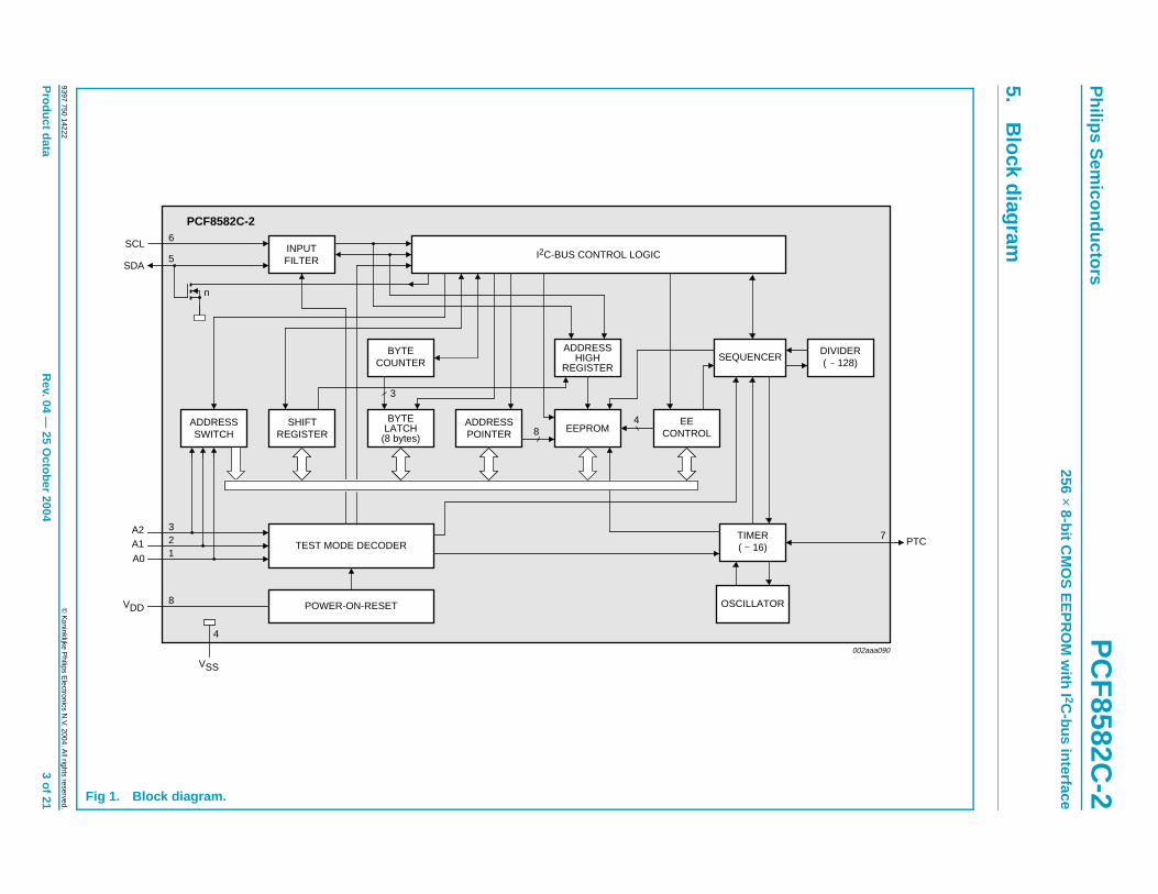
The PCF8582C-2 is a floating gate Electrically Erasable Programmable Read OnlyMemory (EEPROM) with 2 kbits (256 × 8-bit) non-volatile storage. By using aninternal redundant storage code, it is fault tolerant to single bit errors. This featuredramatically increases the reliability compared to conventional EEPROMs. Powerconsumption is low due to the full CMOS technology used. The programming voltageis generated on-chip, using a voltage multiplier.
Data bytes are received and transmitted via the serial I2C-bus. Up to eightPCF8582C-2 devices may be connected to the I2C-bus. Chip select is accomplishedby three address inputs (A0, A1 and A2).
Timing of the E/W cycle is carried out internally, thus no external components arerequired. Programming Time Control (PTC), Pin 7, must be connected to either VDDor left open-circuit. There is an option of using an external clock for timing the lengthof an E/W cycle.
2. Features
Low power CMOS:
2.0 mA maximum operating current
maximum standby current 10 µA (at 6.0 V), typical 4 µA
Non-volatile storage of 2 kbits organized as 256 × 8-bit
Single supply with full operation down to 2.5 V
On-chip voltage multiplier
Serial input/output I2C-bus
Write operations:
byte write mode
8-byte page write mode (minimizes total write time per byte)
Read operations:
sequential read
random read
Internal timer for writing (no external components)
Internal power-on reset
0 kHz to 100 kHz clock frequency
High reliability by using a redundant storage code
Endurance: 1,000,000 Erase/Write (E/W) cycles at Tamb = 22 °C 10 years non-volatile data retention time

Philips Semiconductors PCF8582C-2256 × 8-bit CMOS EEPROM with I 2C-bus interface
Pin and address compatible to: PCF8570, PCF8571, PCF8572, PCA8581 andPCF85102
Pin compatible with a different address to PCF85103
ESD protection exceeds 2000 V HBM per JESD22-A114, 150 V MM perJESD22-A115, and 1000 V CDM per JESD22-C101
Latch-up testing is done to JEDEC Standard JESD78 which exceeds 100 mA
Offered in DIP8 and SO8 packages.
3. Quick reference data
4. Ordering information
4.1 Ordering options
Table 1: Quick reference data
Symbol Parameter Conditions Min Typ Max Unit
VDD supply voltage 2.5 - 6.0 V
IDDR supply current read fSCL = 100 kHz
VDD = 2.5 V - - 60 µA
VDD = 6 V - - 200 µA
IDDW supply current E/W fSCL = 100 kHz
VDD = 2.5 V - - 0.6 mA
VDD = 6 V - - 2.0 mA
IDD(stb) standby supply current VDD = 2.5 V - - 3.5 µA
VDD = 6 V - - 10 µA
Table 2: Ordering information
Type number Package
Name Description Version
PCF8582C-2P/03 DIP8 plastic dual in-line package; 8 leads (300 mil) SOT97-1
PCF8582C-2T/03 SO8 plastic small outline package 8 leads (straight);body width 3.9 mm
SOT96-1
Table 3: Ordering options
Type number Topside mark
PCF8582C-2P/03 PCF8582C-2
PCF8582C-2T/03 8582C-2
Product data Rev. 04 — 25 October 2004 2 of 21
9397 750 14222 © Koninklijke Philips Electronics N.V. 2004. All rights reserved.
xxxx xxxxxxxxxxxxxxxxxxxxxxxxxxxxxx x xxxxxxxxxxxxxx xxxxxxxxxx xxx xxxxxx xxxxxxxxxxxxxxxxxxxxxxx xxxxxxxxxxxxxxxxxxxxxxxxxxx xxxxxx xx xxxxxxxxxxxxxxxxxxxxxxxxxxxxx xxxxxxxxxxxxxxxxxxxxxx xxxxxxxxxxx xxxxxxx xxxxxxxxxxxxxxxxxxxxxxxxxxxxxxxxxxx xxxxxxxxxxxxxx xxxxxx xx xxxxxxxxxxxxxxxxxxxxxxxxxxxxxxxx xxxxxxxxxxxxxxxxxxxxxxxx xxxxxxxxxxxxxxxxxxxxxxxxxxxxxxxxxxxxxxxxxxxxxxxxxxxxx xxxxxxxxxxx xxxxx x x P
hilips Sem
ic
9397750
14222©
Koninklijke P
hilips Electronics N
.V. 2004. All rights reserved.
Product data
Rev. 04 —
25 October 2004
3 of 21
5.B
lock d
onductorsP
CF
8582C-2
256× 8-bit C
MO
S E
EP
RO
M w
ith I2C
-bus interface
iagram
002aaa090
IVIDER 128)
7PTC
Fig 1. Block diagram.
TEST MODE DECODER
POWER-ON-RESET
I2C-BUS CONTROL LOGIC
SEQUENCERADDRESS
HIGHREGISTER
BYTECOUNTER
D(
EECONTROL
TIMER( 16)
EEPROMADDRESSPOINTER
BYTELATCH
(8 bytes)
SHIFTREGISTER
ADDRESSSWITCH
INPUTFILTER
OSCILLATOR
84
3
n
PCF8582C-2
4
VSS
A1A2
A0
321
8VDD
6
5
SCL
SDA

Philips Semiconductors PCF8582C-2256 × 8-bit CMOS EEPROM with I 2C-bus interface
6. Pinning information
6.1 Pinning
6.2 Pin description
7. Device addressing
[1] The Most Significant Bit (MSB) ‘b7’ is sent first.
A2, A1, A0 are hardware selectable pins.
A system could have up to eight PCF8582C-2 devices on the same I2C-bus,equivalent to a 16 kbit EEPROM or 8 pages of 256 bytes of memory.
The eight addresses are defined by the state of the A0, A1, A2 inputs (logic level ‘1’when connected to VDD, logic level ‘0’ when connected to GND). Figure 3 shows thevarious address combinations.
Fig 2. Pin configuration.
1
2
3
4
8
7
6
5
A0
A1
A2
VSS SDA
SCL
PTC
VDD
PCF8582C-2
MGD928
Table 4: Pin description
Symbol Pin Description
A0 1 address input 0
A1 2 address input 1
A2 3 address input 2
VSS 4 negative supply voltage
SDA 5 serial data input/output (I2C-bus)
SCL 6 serial clock input (I2C-bus)
PTC 7 programming time control output
VDD 8 positive supply voltage
Table 5: Device address code
Selection Device code Chip Enable R/W
Bit b7[1] b6 b5 b4 b3 b2 b1 b0
Device 1 0 1 0 A2 A1 A0 R/W
Product data Rev. 04 — 25 October 2004 4 of 21
9397 750 14222 © Koninklijke Philips Electronics N.V. 2004. All rights reserved.

Philips Semiconductors PCF8582C-2256 × 8-bit CMOS EEPROM with I 2C-bus interface
Fig 3. Device addressing.
002aaa246
256-BYTE PAGE
PCF8582C-2DEVICE 1
256-BYTE PAGE
PCF8582C-2DEVICE 2
256-BYTE PAGE
PCF8582C-2DEVICE 3
256-BYTE PAGE
PCF8582C-2DEVICE 4
256-BYTE PAGE
PCF8582C-2DEVICE 5
256-BYTE PAGE
PCF8582C-2DEVICE 6
256-BYTE PAGE
PCF8582C-2DEVICE 7
256-BYTE PAGE
PCF8582C-2DEVICE 8
I2C-BUSA2
0
0
0
0
1
1
1
1
A1
0
0
1
1
0
0
1
1
A0
0
1
0
1
0
1
0
1
Product data Rev. 04 — 25 October 2004 5 of 21
9397 750 14222 © Koninklijke Philips Electronics N.V. 2004. All rights reserved.

Philips Semiconductors PCF8582C-2256 × 8-bit CMOS EEPROM with I 2C-bus interface
8. Functional description
8.1 I2C-bus protocolThe I2C-bus is for 2-way, 2-line communication between different ICs or modules. Theserial bus consists of two bidirectional lines; one for data signals (SDA), and one forclock signals (SCL).
Both the SDA and SCL lines must be connected to a positive supply voltage via apull-up resistor.
The following protocol has been defined:
• Data transfer may be initiated only when the bus is not busy.
• During data transfer, the data line must remain stable whenever the clock line isHIGH. Changes in the data line while the clock line is HIGH will be interpreted ascontrol signals.
8.1.1 Bus conditions
The following bus conditions have been defined:
Bus not busy — Both data and clock lines remain HIGH.
Start data transfer — A change in the state of the data line, from HIGH-to-LOW,while the clock is HIGH, defines the START condition.
Stop data transfer — A change in the state of the data line, from LOW-to-HIGH,while the clock is HIGH, defines the STOP condition.
Data valid — The state of the data line represents valid data when, after a STARTcondition, the data line is stable for the duration of the HIGH period of the clocksignal. There is one clock pulse per bit of data.
8.1.2 Data transfer
Each data transfer is initiated with a START condition and terminated with a STOPcondition. The number of the data bytes, transferred between the START and STOPconditions is limited to 7 bytes in the E/W mode and 8 bytes in the Page E/W mode.
Data transfer is unlimited in the read mode. The information is transmitted in bytesand each receiver acknowledges with a ninth bit.
Within the I2C-bus specifications, a standard-speed mode (100 kHz clock rate) and afast speed mode (400 kHz clock rate) are defined. The PCF8582C-2 operates in onlythe standard-speed mode.
By definition, a device that sends a signal is called a ‘transmitter’, and the devicewhich receives the signal is called a ‘receiver’. The device which controls the signal iscalled the ‘master’. The devices that are controlled by the master are called ‘slaves’.
Each byte is followed by one acknowledge bit. This acknowledge bit is a HIGH level,put on the bus by the transmitter. The master generates an extra acknowledge relatedclock pulse. The slave receiver which is addressed is obliged to generate anacknowledge after the reception of each byte.
Product data Rev. 04 — 25 October 2004 6 of 21
9397 750 14222 © Koninklijke Philips Electronics N.V. 2004. All rights reserved.

Philips Semiconductors PCF8582C-2256 × 8-bit CMOS EEPROM with I 2C-bus interface
The master receiver must generate an acknowledge after the reception of each bytethat has been clocked out of the slave transmitter.
The device that acknowledges has to pull down the SDA line during the acknowledgeclock pulse in such a way that the SDA line is stable LOW during the HIGH period ofthe acknowledge related clock pulse.
Set-up and hold times must be taken into account. A master receiver must signal anend of data to the slave transmitter by not generating an acknowledge on the last bytethat has been clocked out of the slave. In this event, the transmitter must leave thedata line HIGH to enable the master generation of the STOP condition.
8.1.3 Device addressing
Following a START condition, the bus master must output the address of the slave itis accessing. The address of the PCF8582C-2 is shown in Figure 4. To conservepower, no internal pull-up resistors are incorporated on the hardware selectable pinsand they must be connected to either VDD or VSS.
The last bit of the slave address defines the operation to be performed. When set tologic 1, a read operation is selected, while a logic 0 selects a write operation.
8.1.4 Write operations
Byte/word write: For a write operation, the PCF8582C-2 requires a second addressfield. This address field is a word address providing access to the 256 words ofmemory. Upon receipt of the word address, the PCF8582C-2 responds with anacknowledge and awaits the next eight bits of data, again responding with anacknowledge. Word address is automatically incremented. The master can nowterminate the transfer by generating a STOP condition or transmit up to six morebytes of data and then terminate by generating a STOP condition.
After this STOP condition, the E/W cycle starts and the bus is free for anothertransmission. Its duration is 10 ms per byte.
During the E/W cycle the slave receiver does not send an acknowledge bit ifaddressed via the I2C-bus.
Fig 4. Slave address.
002aaa173
1 0 1 0 A2 A1 A0 R/W
FIXED HARDWARESELECTABLE
Product data Rev. 04 — 25 October 2004 7 of 21
9397 750 14222 © Koninklijke Philips Electronics N.V. 2004. All rights reserved.

Philips Semiconductors PCF8582C-2256 × 8-bit CMOS EEPROM with I 2C-bus interface
Page write: The PCF8582C-2 is capable of an eight-byte page write operation. It isinitiated in the same manner as the byte write operation. The master can transit eightdata bytes within one transmission. After receipt of each byte, the PCF8582C-2 willrespond with an acknowledge. The typical E/W time in this mode is9 × 3.5 ms = 31.5 ms. Erasing a block of 8 bytes in page mode takes typical 3.5 msand sequential writing of these 8 bytes another typical 28 ms.
After the receipt of each data byte, the three low-order bits of the word address areinternally incremented. The high-order five bits of the address remain unchanged.The slave acknowledges the reception of each data byte with an ACK. The I2C-busdata transfer is terminated by the master after the 8th byte with a STOP condition. Ifthe master transmits more than eight bytes prior to generating the STOP condition,no acknowledge will be given on the ninth (and following) data bytes and the wholetransmission will be ignored and no programming will be done. As in the byte writeoperation, all inputs are disabled until completion of the internal write cycles.
Fig 5. Auto-increment memory word address; two byte write.
S 0 ASLAVE ADDRESS WORD ADDRESS A ADATA P
acknowledgefrom slave
acknowledgefrom slave
acknowledgefrom slave
acknowledgefrom slave
ADATA
R/Wauto incrementword address
auto incrementword address
MBA701
Fig 6. Page write operation; eight bytes.
S 0 ASLAVE ADDRESS WORD ADDRESS A ADATA N
acknowledgefrom slave
acknowledgefrom slave
acknowledgefrom slave
R/Wauto incrementword address
acknowledgefrom slave
ADATA N + 1
auto incrementword address
002aaa245
A
acknowledgefrom slave
ADATA N + 7
auto incrementword address
last byte
Product data Rev. 04 — 25 October 2004 8 of 21
9397 750 14222 © Koninklijke Philips Electronics N.V. 2004. All rights reserved.

Philips Semiconductors PCF8582C-2256 × 8-bit CMOS EEPROM with I 2C-bus interface
8.1.5 Read operations
Read operations are initiated in the same manner as write operations with theexception that the LSB of the slave address is set to logic 1.
There are three basic read operations: current address read, random read, andsequential read.
Remark: The lower 8 bits of the word address are incremented after eachtransmission of a data byte (read or write). The MSB of the word address, which isdefined in the slave address, is not changed when the word address count overflows.Thus, the word address overflows from 255 to 0, and from 511 to 256.
Fig 7. Master reads PCF8582C-2 slave after setting word address (write word address; read data);sequential read.
S 0 ASLAVE ADDRESS WORD ADDRESS A ASLAVE ADDRESS
acknowledgefrom slave
acknowledgefrom slave
acknowledgefrom slave
R/W
acknowledgefrom master
ADATA
auto incrementword address
MBA703
P
no acknowledgefrom master
1DATA
auto incrementword address
last byte
R/W
S 1
n bytesat this moment mastertransmitter becomesmaster receiver andEEPROM slave receiverbecomes slave transmitter
Fig 8. Master reads PCF8582C-2 immediately after first byte (read mode); current address read.
S 1 ASLAVE ADDRESS DATA A 1DATA
acknowledgefrom slave
acknowledgefrom master
no acknowledgefrom master
R/Wauto incrementword address
MBA704 - 1
auto incrementword address
n bytes last bytes
P
Product data Rev. 04 — 25 October 2004 9 of 21
9397 750 14222 © Koninklijke Philips Electronics N.V. 2004. All rights reserved.

Philips Semiconductors PCF8582C-2256 × 8-bit CMOS EEPROM with I 2C-bus interface
9. Limiting values
10. Characteristics
Table 6: Limiting valuesIn accordance with the Absolute Maximum Rating System (IEC 60134).
Symbol Parameter Conditions Min Max Unit
VDD supply voltage −0.3 +6.5 V
Vi input voltage on any input pin |Zi| > 500 Ω VSS − 0.8 +6.5 V
Ii input current on any input pin - 1 mA
Io output current - 10 mA
Tstg storage temperature −65 +150 °C
Tamb operating ambient temperature −40 +85 °C
Table 7: CharacteristicsVDD = 2.5 to 6.0 V; VSS = 0 V; Tamb = −40 to +85 °C; unless otherwise specified.
Symbol Parameter Conditions Min Typ Max Unit
Supplies
VDD supply voltage 2.5 - 6.0 V
IDDR supply current read fSCL = 100 kHz
VDD = 2.5 V - - 60 µA
VDD = 6.0 V - - 200 µA
IDDW supply current E/W fSCL = 100 kHz
VDD = 2.5 V - - 0.6 mA
VDD = 6.0 V - - 2.0 mA
IDD(stb) standby supply current VDD = 2.5 V - - 3.5 µA
VDD = 6.0 V - - 10 µA
PTC output (pin 7)
VIL LOW level input voltage −0.8 - 0.1VDD V
VIH HIGH level input voltage 0.9VDD - VDD + 0.8 V
SCL input (pin 6)
VIL LOW level input voltage −0.8 - 0.3VDD V
VIH HIGH level input voltage 0.7VDD - +6.5 V
ILI input leakage current VI = VDD or VSS - - ±1 µA
fSCL clock input frequency 0 - 100 kHz
Ci input capacitance VI = VSS - - 7 pF
Product data Rev. 04 — 25 October 2004 10 of 21
9397 750 14222 © Koninklijke Philips Electronics N.V. 2004. All rights reserved.

Philips Semiconductors PCF8582C-2256 × 8-bit CMOS EEPROM with I 2C-bus interface
11. I2C-bus characteristics
[1] The hold time required (not greater than 300 ns) to bridge the undefined region of the falling edge of SCL must be internally provided bya transmitter.
SDA input/output (pin 5)
VIL LOW level input voltage −0.8 - 0.3VDD V
VIH HIGH level input voltage 0.7VDD - +6.5 V
VOL LOW level output voltage IOL = 3 mA; VDD(min) - - 0.4 V
ILO output leakage current VOH = VDD - - 1 µA
Ci input capacitance VI = VSS - - 7 pF
Data retention time
tS data retention time Tamb = 55 °C 10 − − years
Table 7: Characteristics …continuedVDD = 2.5 to 6.0 V; VSS = 0 V; Tamb = −40 to +85 °C; unless otherwise specified.
Symbol Parameter Conditions Min Typ Max Unit
Table 8: I 2C-bus characteristicsAll of the timing values are valid within the operating supply voltage and ambient temperature range and refer to VIL and VIHwith an input voltage swing from VSS to VDD; see Figure 9.
Symbol Parameter Conditions Min Max Unit
fSCL clock frequency 0 100 kHz
tBUF bus free time between a STOP andSTART condition
4.7 − µs
tHD;STA START condition hold time afterwhich first clock pulse is generated
4.0 − µs
tLOW LOW level clock period 4.7 − µs
tHIGH HIGH level clock period 4.0 − µs
tSU;STA set-up time for START condition repeated start 4.7 − µs
tHD;DAT data hold time
for bus compatible masters 5 − µs
for bus devices [1] 0 − ns
tSU;DAT data set-up time 250 − ns
tr SDA and SCL rise time − 1 µs
tf SDA and SCL fall time − 300 ns
tSU;STO set-up time for STOP condition 4.0 − µs
Product data Rev. 04 — 25 October 2004 11 of 21
9397 750 14222 © Koninklijke Philips Electronics N.V. 2004. All rights reserved.

Philips Semiconductors PCF8582C-2256 × 8-bit CMOS EEPROM with I 2C-bus interface
12. Write cycle limits
13. External clock timing
P = STOP condition; S = START condition.
Fig 9. Timing requirements for the I 2C-bus.
MBA705
t BUF
HD;STAt
SCL
SDA
P S
t LOW
t r HD;DATt SU;DATt
t f
t HIGH
S
HD;STAt
SU;STAt SU;STOt
P
Table 9: Write cycle limitsSelection of the chip address is achieved by connecting the A0, A1 and A2 inputs to either VSS or VDD.
Symbol Parameter Conditions Min Typ Max Unit
E/W cycle timing
tE/W E/W cycle time internal oscillator − 7 − ms
external clock 4 − 10 ms
Endurance
NE/W E/W cycle per byte Tamb = −40 °C to +85 °C 100000 − − cycles
Tamb = 22 °C 1000000 − cycles
Fig 10. One byte E/W cycle.
td tHIGHftrt
LOWt
STOP
1 2 257PTC
SDA
SCL
MBA697
Product data Rev. 04 — 25 October 2004 12 of 21
9397 750 14222 © Koninklijke Philips Electronics N.V. 2004. All rights reserved.
Philips Semiconductors PCF8582C-2256 × 8-bit CMOS EEPROM with I 2C-bus interface
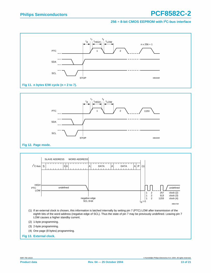
Fig 11. n bytes E/W cycle (n = 2 to 7).
td tHIGHftrt
LOWt
STOP
1 2PTC
SDA
SCL
MBA698
n x 256 + 1
Fig 12. Page mode.
td tHIGHftrt
LOWt
STOP
1 2PTC
SDA
SCL
MBA699
1153
(1) If an external clock is chosen, this information is latched internally by setting pin 7 (PTC) LOW after transmission of theeighth bits of the word address (negative edge of SCL). Thus the state of pin 7 may be previously undefined. Leaving pin 7LOW causes a higher standby current.
(2) 1-byte programming.
(3) 2-byte programming.
(4) One page (8 bytes) programming.
Fig 13. External clock.
S 0 A A DATA A DATA A P
SLAVE ADDRESS WORD ADDRESS
(1)
undefined
111
222
257513
1153
clock (2)clock (3)clock (4)
dt 0negative edge
SCL 8-bit
undefinedLOW
HIGHPTC
2I C-bus
MBA700
Product data Rev. 04 — 25 October 2004 13 of 21
9397 750 14222 © Koninklijke Philips Electronics N.V. 2004. All rights reserved.

Philips Semiconductors PCF8582C-2256 × 8-bit CMOS EEPROM with I 2C-bus interface
14. Package outline
Fig 14. DIP8 package outline (SOT97-1).
REFERENCESOUTLINEVERSION
EUROPEANPROJECTION ISSUE DATE
IEC JEDEC JEITA
SOT97-199-12-2703-02-13
UNIT Amax.
1 2 b1(1) (1) (1)
b2 c D E e M ZHL
mm
DIMENSIONS (inch dimensions are derived from the original mm dimensions)
A min.
A max. b
max.wMEe1
1.731.14
0.530.38
0.360.23
9.89.2
6.486.20
3.603.05
0.2542.54 7.628.257.80
10.08.3
1.154.2 0.51 3.2
inches 0.0680.045
0.0210.015
0.0140.009
1.070.89
0.0420.035
0.390.36
0.260.24
0.140.12
0.010.1 0.30.320.31
0.390.33
0.0450.17 0.02 0.13
b2
050G01 MO-001 SC-504-8
MH
c
(e )1
ME
A
L
seat
ing
plan
e
A1
w Mb1
e
D
A2
Z
8
1
5
4
b
E
0 5 10 mm
scale
Note
1. Plastic or metal protrusions of 0.25 mm (0.01 inch) maximum per side are not included.
pin 1 index
DIP8: plastic dual in-line package; 8 leads (300 mil) SOT97-1
Product data Rev. 04 — 25 October 2004 14 of 21
9397 750 14222 © Koninklijke Philips Electronics N.V. 2004. All rights reserved.
Philips Semiconductors PCF8582C-2256 × 8-bit CMOS EEPROM with I 2C-bus interface
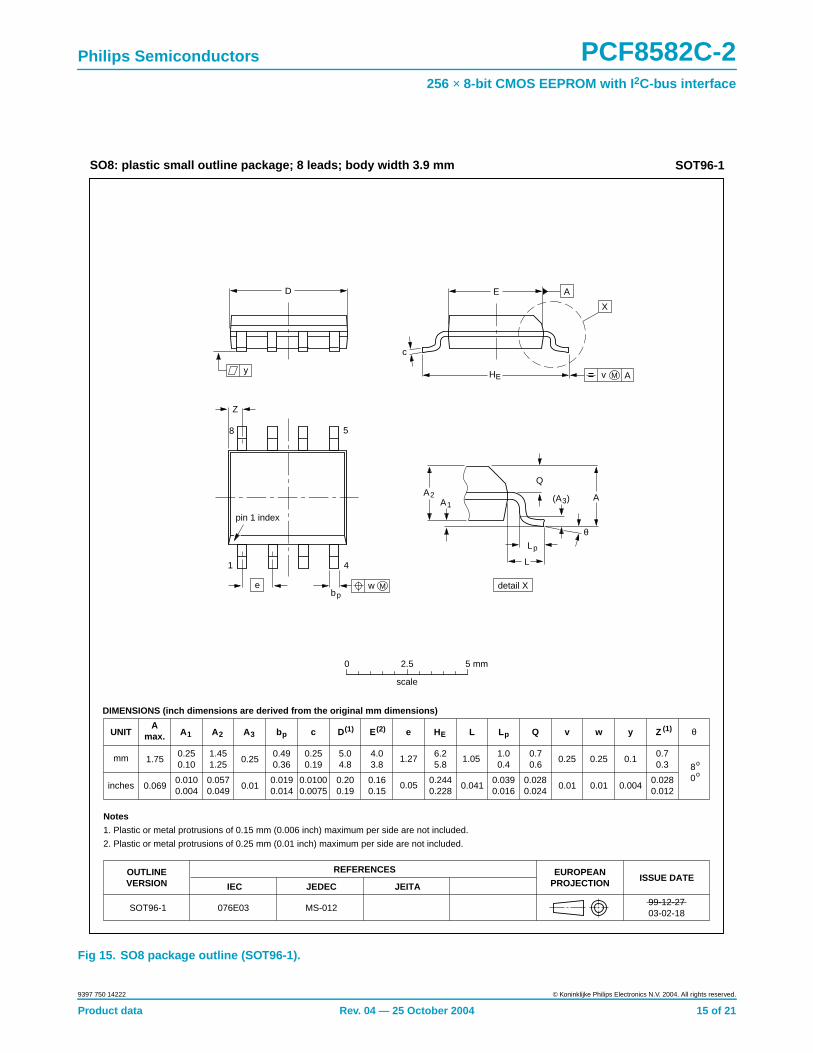
Fig 15. SO8 package outline (SOT96-1).
UNITA
max. A1 A2 A3 bp c D(1) E(2) (1)e HE L L p Q Zywv θ
REFERENCESOUTLINEVERSION
EUROPEANPROJECTION ISSUE DATE
IEC JEDEC JEITA
mm
inches
1.750.250.10
1.451.25
0.250.490.36
0.250.19
5.04.8
4.03.8
1.276.25.8
1.050.70.6
0.70.3 8
0
o
o
0.25 0.10.25
DIMENSIONS (inch dimensions are derived from the original mm dimensions)
Notes
1. Plastic or metal protrusions of 0.15 mm (0.006 inch) maximum per side are not included.
2. Plastic or metal protrusions of 0.25 mm (0.01 inch) maximum per side are not included.
1.00.4
SOT96-1
X
w M
θ
AA1
A2
bp
D
HE
Lp
Q
detail X
E
Z
e
c
L
v M A
(A )3
A
4
5
pin 1 index
1
8
y
076E03 MS-012
0.0690.0100.004
0.0570.049
0.010.0190.014
0.01000.0075
0.200.19
0.160.15
0.050.2440.228
0.0280.024
0.0280.012
0.010.010.041 0.0040.0390.016
0 2.5 5 mm
scale
SO8: plastic small outline package; 8 leads; body width 3.9 mm SOT96-1
99-12-2703-02-18
Product data Rev. 04 — 25 October 2004 15 of 21
9397 750 14222 © Koninklijke Philips Electronics N.V. 2004. All rights reserved.

Philips Semiconductors PCF8582C-2256 × 8-bit CMOS EEPROM with I 2C-bus interface
15. Soldering
15.1 IntroductionThis text gives a very brief insight to a complex technology. A more in-depth accountof soldering ICs can be found in our Data Handbook IC26; Integrated CircuitPackages (document order number 9398 652 90011).
There is no soldering method that is ideal for all IC packages. Wave soldering is oftenpreferred when through-hole and surface mount components are mixed on oneprinted-circuit board. Wave soldering can still be used for certain surface mount ICs,but it is not suitable for fine pitch SMDs. In these situations reflow soldering isrecommended. Driven by legislation and environmental forces the worldwide use oflead-free solder pastes is increasing.
15.2 Through-hole mount packages
15.2.1 Soldering by dipping or by solder wave
Typical dwell time of the leads in the wave ranges from 3 to 4 seconds at 250 °C or265 °C, depending on solder material applied, SnPb or Pb-free respectively.
The total contact time of successive solder waves must not exceed 5 seconds.
The device may be mounted up to the seating plane, but the temperature of theplastic body must not exceed the specified maximum storage temperature (Tstg(max)).If the printed-circuit board has been pre-heated, forced cooling may be necessaryimmediately after soldering to keep the temperature within the permissible limit.
15.2.2 Manual soldering
Apply the soldering iron (24 V or less) to the lead(s) of the package, either below theseating plane or not more than 2 mm above it. If the temperature of the soldering ironbit is less than 300 °C it may remain in contact for up to 10 seconds. If the bittemperature is between 300 and 400 °C, contact may be up to 5 seconds.
15.3 Surface mount packages
15.3.1 Reflow soldering
Reflow soldering requires solder paste (a suspension of fine solder particles, flux andbinding agent) to be applied to the printed-circuit board by screen printing, stencillingor pressure-syringe dispensing before package placement.
Several methods exist for reflowing; for example, convection or convection/infraredheating in a conveyor type oven. Throughput times (preheating, soldering andcooling) vary between 100 and 200 seconds depending on heating method.
Typical reflow peak temperatures range from 215 to 270 °C depending on solderpaste material. The top-surface temperature of the packages should preferably bekept:
• below 225 °C (SnPb process) or below 245 °C (Pb-free process)
– for all the BGA and SSOP-T packages
Product data Rev. 04 — 25 October 2004 16 of 21
9397 750 14222 © Koninklijke Philips Electronics N.V. 2004. All rights reserved.

Philips Semiconductors PCF8582C-2256 × 8-bit CMOS EEPROM with I 2C-bus interface
– for packages with a thickness ≥ 2.5 mm
– for packages with a thickness < 2.5 mm and a volume ≥ 350 mm3 so calledthick/large packages.
• below 240 °C (SnPb process) or below 260 °C (Pb-free process) for packages witha thickness < 2.5 mm and a volume < 350 mm3 so called small/thin packages.
Moisture sensitivity precautions, as indicated on packing, must be respected at alltimes.
15.3.2 Wave soldering
Conventional single wave soldering is not recommended for surface mount devices(SMDs) or printed-circuit boards with a high component density, as solder bridgingand non-wetting can present major problems.
To overcome these problems the double-wave soldering method was specificallydeveloped.
If wave soldering is used the following conditions must be observed for optimalresults:
• Use a double-wave soldering method comprising a turbulent wave with highupward pressure followed by a smooth laminar wave.
• For packages with leads on two sides and a pitch (e):
– larger than or equal to 1.27 mm, the footprint longitudinal axis is preferred to beparallel to the transport direction of the printed-circuit board;
– smaller than 1.27 mm, the footprint longitudinal axis must be parallel to thetransport direction of the printed-circuit board.
The footprint must incorporate solder thieves at the downstream end.
• For packages with leads on four sides, the footprint must be placed at a 45° angleto the transport direction of the printed-circuit board. The footprint mustincorporate solder thieves downstream and at the side corners.
During placement and before soldering, the package must be fixed with a droplet ofadhesive. The adhesive can be applied by screen printing, pin transfer or syringedispensing. The package can be soldered after the adhesive is cured.
Typical dwell time of the leads in the wave ranges from 3 to 4 seconds at 250 °C or265 °C, depending on solder material applied, SnPb or Pb-free respectively.
A mildly-activated flux will eliminate the need for removal of corrosive residues inmost applications.
15.3.3 Manual soldering
Fix the component by first soldering two diagonally-opposite end leads. Use a lowvoltage (24 V or less) soldering iron applied to the flat part of the lead. Contact timemust be limited to 10 seconds at up to 300 °C.
When using a dedicated tool, all other leads can be soldered in one operation within2 to 5 seconds between 270 and 320 °C.
Product data Rev. 04 — 25 October 2004 17 of 21
9397 750 14222 © Koninklijke Philips Electronics N.V. 2004. All rights reserved.

Philips Semiconductors PCF8582C-2256 × 8-bit CMOS EEPROM with I 2C-bus interface
15.4 Package related soldering information
[1] For more detailed information on the BGA packages refer to the (LF)BGA Application Note(AN01026); order a copy from your Philips Semiconductors sales office.
[2] All surface mount (SMD) packages are moisture sensitive. Depending upon the moisture content, themaximum temperature (with respect to time) and body size of the package, there is a risk that internalor external package cracks may occur due to vaporization of the moisture in them (the so calledpopcorn effect). For details, refer to the Drypack information in the Data Handbook IC26; IntegratedCircuit Packages; Section: Packing Methods.
[3] For SDIP packages, the longitudinal axis must be parallel to the transport direction of theprinted-circuit board.
[4] Hot bar soldering or manual soldering is suitable for PMFP packages.
[5] These transparent plastic packages are extremely sensitive to reflow soldering conditions and muston no account be processed through more than one soldering cycle or subjected to infrared reflowsoldering with peak temperature exceeding 217 °C ± 10 °C measured in the atmosphere of the reflowoven. The package body peak temperature must be kept as low as possible.
[6] These packages are not suitable for wave soldering. On versions with the heatsink on the bottomside, the solder cannot penetrate between the printed-circuit board and the heatsink. On versions withthe heatsink on the top side, the solder might be deposited on the heatsink surface.
[7] If wave soldering is considered, then the package must be placed at a 45° angle to the solder wavedirection. The package footprint must incorporate solder thieves downstream and at the side corners.
[8] Wave soldering is suitable for LQFP, QFP and TQFP packages with a pitch (e) larger than 0.8 mm; itis definitely not suitable for packages with a pitch (e) equal to or smaller than 0.65 mm.
[9] Wave soldering is suitable for SSOP and TSSOP packages with a pitch (e) equal to or larger than0.65 mm; it is definitely not suitable for packages with a pitch (e) equal to or smaller than 0.5 mm.
Table 10: Suitability of IC packages for wave, reflow and dipping soldering methods
Mounting Package [1] Soldering method
Wave Reflow [2] Dipping
Through-holemount
DBS, DIP, HDIP, RDBS,SDIP, SIL
suitable[3] − suitable
Through-hole-surface mount
PMFP[4] not suitable notsuitable
−
Surface mount BGA, LBGA, LFBGA,SQFP, SSOP-T[5],TFBGA, VFBGA
not suitable suitable −
DHVQFN, HBCC, HBGA,HLQFP, HSQFP, HSOP,HTQFP, HTSSOP,HVQFN, HVSON, SMS
not suitable[6] suitable −
PLCC[7], SO, SOJ suitable suitable −
LQFP, QFP, TQFP not recommended[7][8] suitable −
SSOP, TSSOP, VSO,VSSOP
not recommended[9] suitable −
Product data Rev. 04 — 25 October 2004 18 of 21
9397 750 14222 © Koninklijke Philips Electronics N.V. 2004. All rights reserved.

Philips Semiconductors PCF8582C-2256 × 8-bit CMOS EEPROM with I 2C-bus interface
16. Revision history
Table 11: Revision history
Rev Date CPCN Description
04 20041025 - Product data (9397 750 14222).
Modifications:
• Section 8.1.2 “Data transfer” on page 6, third paragraph: change ‘high-speed’ to‘standard-speed’ (2 places).
03 20031006 - Product data (9397 750 12029). ECN 853-2338 30407 dated 02 October 2003.
02 20020509 - Product data; second version (0397 750 08536). Supersedes data in data sheetPCF85xxC-2 family dated 1997 Feb 13 (9397 750 01773). Engineering Change Notice853-2338 28170 dated 09 May 2002.
01 19970213 - Product data; initial version (as PCF85xxC-2 family , 9397 750 01773).
Product data Rev. 04 — 25 October 2004 19 of 21
9397 750 14222 © Koninklijke Philips Electronics N.V. 2004. All rights reserved.

Philips Semiconductors PCF8582C-2256 × 8-bit CMOS EEPROM with I 2C-bus interface
17. Data sheet status
[1] Please consult the most recently issued data sheet before initiating or completing a design.
[2] The product status of the device(s) described in this data sheet may have changed since this data sheet was published. The latest information is available on the Internet atURL http://www.semiconductors.philips.com.
[3] For data sheets describing multiple type numbers, the highest-level product status determines the data sheet status.
18. Definitions
Short-form specification — The data in a short-form specification isextracted from a full data sheet with the same type number and title. Fordetailed information see the relevant data sheet or data handbook.
Limiting values definition — Limiting values given are in accordance withthe Absolute Maximum Rating System (IEC 60134). Stress above one ormore of the limiting values may cause permanent damage to the device.These are stress ratings only and operation of the device at these or at anyother conditions above those given in the Characteristics sections of thespecification is not implied. Exposure to limiting values for extended periodsmay affect device reliability.
Application information — Applications that are described herein for anyof these products are for illustrative purposes only. Philips Semiconductorsmake no representation or warranty that such applications will be suitable forthe specified use without further testing or modification.
19. Disclaimers
Life support — These products are not designed for use in life supportappliances, devices, or systems where malfunction of these products canreasonably be expected to result in personal injury. Philips Semiconductors
customers using or selling these products for use in such applications do soat their own risk and agree to fully indemnify Philips Semiconductors for anydamages resulting from such application.
Right to make changes — Philips Semiconductors reserves the right tomake changes in the products - including circuits, standard cells, and/orsoftware - described or contained herein in order to improve design and/orperformance. When the product is in full production (status ‘Production’),relevant changes will be communicated via a Customer Product/ProcessChange Notification (CPCN). Philips Semiconductors assumes noresponsibility or liability for the use of any of these products, conveys nolicence or title under any patent, copyright, or mask work right to theseproducts, and makes no representations or warranties that these products arefree from patent, copyright, or mask work right infringement, unless otherwisespecified.
20. Licenses
Level Data sheet status [1] Product status [2][3] Definition
I Objective data Development This data sheet contains data from the objective specification for product development. PhilipsSemiconductors reserves the right to change the specification in any manner without notice.
II Preliminary data Qualification This data sheet contains data from the preliminary specification. Supplementary data will be publishedat a later date. Philips Semiconductors reserves the right to change the specification without notice, inorder to improve the design and supply the best possible product.
III Product data Production This data sheet contains data from the product specification. Philips Semiconductors reserves theright to make changes at any time in order to improve the design, manufacturing and supply. Relevantchanges will be communicated via a Customer Product/Process Change Notification (CPCN).
Purchase of Philips I 2C components
Purchase of Philips I2C components conveys a licenseunder the Philips’ I2C patent to use the components in theI2C system provided the system conforms to the I2Cspecification defined by Philips. This specification can beordered using the code 9398 393 40011.
9397 750 14222 © Koninklijke Philips Electronics N.V. 2004. All rights reserved.
Product data Rev. 04 — 25 October 2004 20 of 21
Contact informationFor additional information, please visit http://www.semiconductors.philips.com .For sales office addresses, send e-mail to: [email protected] . Fax: +31 40 27 24825

© Koninklijke Philips Electronics N.V. 2004.Printed in the U.S.A.
All rights are reserved. Reproduction in whole or in part is prohibited without the priorwritten consent of the copyright owner.
The information presented in this document does not form part of any quotation orcontract, is believed to be accurate and reliable and may be changed without notice. Noliability will be accepted by the publisher for any consequence of its use. Publicationthereof does not convey nor imply any license under patent- or other industrial orintellectual property rights.
Date of release: 25 October 2004 Document order number: 9397 750 14222
Contents
Philips Semiconductors PCF8582C-2256 × 8-bit CMOS EEPROM with I 2C-bus interface
1 Description . . . . . . . . . . . . . . . . . . . . . . . . . . . . . 12 Features . . . . . . . . . . . . . . . . . . . . . . . . . . . . . . . 13 Quick reference data . . . . . . . . . . . . . . . . . . . . . 24 Ordering information . . . . . . . . . . . . . . . . . . . . . 24.1 Ordering options . . . . . . . . . . . . . . . . . . . . . . . . 25 Block diagram . . . . . . . . . . . . . . . . . . . . . . . . . . 36 Pinning information . . . . . . . . . . . . . . . . . . . . . . 46.1 Pinning . . . . . . . . . . . . . . . . . . . . . . . . . . . . . . . 46.2 Pin description . . . . . . . . . . . . . . . . . . . . . . . . . 47 Device addressing . . . . . . . . . . . . . . . . . . . . . . . 48 Functional description . . . . . . . . . . . . . . . . . . . 68.1 I2C-bus protocol . . . . . . . . . . . . . . . . . . . . . . . . 68.1.1 Bus conditions . . . . . . . . . . . . . . . . . . . . . . . . . 68.1.2 Data transfer . . . . . . . . . . . . . . . . . . . . . . . . . . . 68.1.3 Device addressing . . . . . . . . . . . . . . . . . . . . . . 78.1.4 Write operations . . . . . . . . . . . . . . . . . . . . . . . . 78.1.5 Read operations . . . . . . . . . . . . . . . . . . . . . . . . 99 Limiting values. . . . . . . . . . . . . . . . . . . . . . . . . 1010 Characteristics . . . . . . . . . . . . . . . . . . . . . . . . . 1011 I2C-bus characteristics . . . . . . . . . . . . . . . . . . 1112 Write cycle limits . . . . . . . . . . . . . . . . . . . . . . . 1213 External clock timing. . . . . . . . . . . . . . . . . . . . 1214 Package outline . . . . . . . . . . . . . . . . . . . . . . . . 1415 Soldering . . . . . . . . . . . . . . . . . . . . . . . . . . . . . 1615.1 Introduction . . . . . . . . . . . . . . . . . . . . . . . . . . 1615.2 Through-hole mount packages . . . . . . . . . . . . 1615.2.1 Soldering by dipping or by solder wave . . . . . 1615.2.2 Manual soldering . . . . . . . . . . . . . . . . . . . . . . 1615.3 Surface mount packages . . . . . . . . . . . . . . . . 1615.3.1 Reflow soldering . . . . . . . . . . . . . . . . . . . . . . . 1615.3.2 Wave soldering . . . . . . . . . . . . . . . . . . . . . . . . 1715.3.3 Manual soldering . . . . . . . . . . . . . . . . . . . . . . 1715.4 Package related soldering information . . . . . . 1816 Revision history . . . . . . . . . . . . . . . . . . . . . . . . 1917 Data sheet status . . . . . . . . . . . . . . . . . . . . . . . 2018 Definitions . . . . . . . . . . . . . . . . . . . . . . . . . . . . 2019 Disclaimers. . . . . . . . . . . . . . . . . . . . . . . . . . . . 2020 Licenses . . . . . . . . . . . . . . . . . . . . . . . . . . . . . . 20