I2C Bus Serial EEPROM Driver using GPIO -...
22
Texas Instruments Inc., January 2002 I2C Bus Serial EEPROM Driver using GPIO Module & Software Test Bench (STB) user’s Guide C28x Foundation Software
Transcript of I2C Bus Serial EEPROM Driver using GPIO -...

Texas Instruments Inc., January 2002
I2C Bus Serial EEPROM Driver using GPIO
Module & Software Test Bench (STB) user’s Guide
C28x Foundation Software

Texas Instruments Inc., January 2002

Texas Instruments Inc., January 2002
CCCooonnnttteeennntttsss Chapter I: Module details
1. I2CSE2P_IO: I2C bus serial EEPROM driver using GPIO………....………………..………….…1
Chapter 2. Software Test Bench
1. Software Test Bench (STB) overview………………………………….………………..………….13
2. Directory structure…………………………………….………………………………………………15
3. Hardware Setup..……………………………………………………………………………………...16
4. Address length selection……………………………………………………………………………..16
5. Loading and building CC project for I2CSE2P_IO demo………………..………………………..17

Texas Instruments Inc., January 2002

Texas Instruments Inc., January 2002 1
Description This module implements the I2C bus serial EEPROM driver using virtual
I2C module (GPIO based). Availability C-Callable Assembly (CcA) Module Properties Type: Target Dependent, Application Dependent Target Devices: x28xx
C-Callable file names: i2cse2pd.c, i2cse2pu.c, i2cm_io.asm, i2cmu.c, i2cse2p.h, i2cm_io.h & i2cmpin.h
Item C-Callable ASM Comments
Code Sizeÿ 554 words (.text) + 36 words (.switch)
Data RAM 13 words (.bss)
xDAIS ready No xDAIS component No
Multiple instances No Reentrancy No
Multiple Invocation
No
Stack usage 0 words
ÿ Code size mentioned here is sum of init & tick functions.
Note: The I2C bus serial EEPROM utilities viz., i2cSe2pFree(), i2cSe2pWrite(), i2cSe2pRead() take 33 words of program memory.
I2C bus serial EEPROM driver using virtual I2C (GPIO based) I2CSE2P_IO
APIs
I2CSE2P_IO (GPIO based)
SDA
SCL
R R
VCC

Texas Instruments Inc., January 2002 2
C/C-Callable ASM Interface C/C-Callable ASM Interface Object Definition
typedef struct { I2CSE2P_DATA msgPtr; /* Message pointer */ unsigned int csr; /* Control and Status register */ void (*init)(void *); /* Driver Initialization routine */ void (*tick)(void *); /* I2C bus EEPROM tick */
}I2CSE2P_IO; I2C Serial EEPROM Message Definition typedef struct { unsigned int *dataPtr; /* Data pointer */ unsigned int nrData; /* number of data */ unsigned int addr; /* Address */ unsigned int Did_Blknr; /* Device select and/or Block select bits */
}I2CSE2P_DATA; Module Terminal Variables
Item Name Description Format Range(Hex) Register csr Control and Status register - -
Input msgPtr Handle to the EEPROM message - -
Message parameters
Item Name Description Format Range(Hex) Did_Blknr Device select and/or Block select bits Q0 0-7
addr Address location within the EEPROM - -
dataPtr Pointer to the data array - -
Attributes
nrData Number of data in the data array - -
Special Constants and Data types I2CSE2P_IO
The module definition is created as a data type. This makes it convenient to instance an interface to the virtual I2C master driver. Multiple instantiation is not allowed for driver modules. I2CSE2P_DATA The message definition is created as a data type. This makes it convenient to instance multiple messages. I2CSE2P_IO_handle User defined data type of pointer to I2CSE2P_IO Module
I2CSE2P_IO_DEFAULTS This symbolic constant is used to initialize the I2CSE2P_IO Module. This provides the initial values to the terminal variables as well as method pointers.

Texas Instruments Inc., January 2002 3
C/C-Callable ASM Interface
Write Sequence Following the START condition, the control byte with the direction bit set to logic “0” for write operation is sent to the I2C bus serial EEPROM. The driver checks for acknowledge from the EEPROM, if acknowledge is not generated by the EEPROM device, then the driver will issue STOP condition and re-try again. If acknowledged by the serial EEPROM, the address byte is transmitted (one or two) and it will be written to the internal address pointer register of serial EEPROM. After receiving another acknowledge signal, data bytes are transmitted to the serial EEPROM that are temporarily stored in the page buffer and will be written into the memory starting at the address value in the internal address register after the master has transmitted a STOP condition. If acknowledge was not generated by the EEPROM during the address or data transmission, the slave driver sets ERROR flag in control and status register and exits. Caution: Write operation limited to writing bytes within a single physical page (page size depends on device) regardless of the number of bytes actually being written. Physical page boundary starts at addresses that are integer multiple of the page buffer size (or page size) and end address that are integer multiples of page size minus one (page size-1). If write command attempts to write across a physical page boundary, the result is that the data wraps around to the beginning of the current page (overwriting data previously stored there), instead of being written to next page as might be expected. It is therefore necessary for the application software to prevent write operations that would attempt to cross page boundary.
Write sequence for device up to 16Kbits storage capacity (One Byte address):
Write sequence for devices grater then 16Kbits storage capacity (Two byte address):

Texas Instruments Inc., January 2002 4
C/C-Callable ASM Interface
Read Sequence To perform read operation, first address must be written into the internal address register of serial EEPROM. This is done by sending the word address to the serial EEPROM as part of write operation. After the word address is sent, the driver generates a repeat START condition following acknowledge. This terminates the write operation but not before the internal address register is set. Then the driver issues the control byte with direction bit set to ‘1” for read operation. The driver checks for acknowledge from the EEPROM and starts reading the 8-bit data word from serial EEPROM. After reading the 8-bit data, the driver issues acknowledge to serial EEPROM. This directs the serial EEPROM to transmit the next sequentially addressed 8-bit word. After reading all the data bytes acknowledge is not issued to the serial EEPROM and generates STOP condition to terminate the data transfer.
Read sequence for device up to 16Kbits storage capacity (One byte address)
Read sequence for device grater then 16Kbits storage capacity (Two byte address)

Texas Instruments Inc., January 2002 5
C/C-Callable ASM Interface Device Addressing
A control byte is the first byte transmitted following the start condition. This control byte has the following three primary functions.
• Identify the serial EEPROM as the slave addressed on the bus (4bits). • Select the specific serial EEPROM and/or the internal memory blocks on the bus.
There may be up to 8 serial EEPROMs on the bus (3bits). • Select READ or WRITE function for the next command transmitted by the master.
Control Byte:
a). I2C Slave Address (Must be 1010 for memory) Since there is not a chip select pin, the part is selected by four-bit code in the control byte to identify the type of product. The four-bit code was established by Philips for I2C protocol. A 1010 code identifies the slave device as a serial EEPROM. The serial EEPROM will remain in stand-by until the 1010 code is transmitted on the bus. Other non serial EEPROM slave device will not respond to the 1010 code on the bus. b). Chip and/or block select bits The next three control bits are utilized for the chip selection and/or internal block selection. The standard I2C protocol was proposed to allow up to 16K bits ( 82 ×k ) of memory to be selected. This could be accomplished by accessing combination of devices or blocks within a device, as shown in the below table. These 3-bits for this select must match the hardware conditions (IF ANY ARE USED) of the external A0, A1 & A2 pins or the internal block address. Store the 3-bit values that are to be transferred in this time slot in Did_Blknr attributes of I2C message object.
Device (MICROCHIP part no)
K bits Density
Internal Blocks
A2 Pin
A1 Pin
A0 Pin
Bus Access Devices
24LC01B 1 )8128( × 1 H or L H or L H or L Up to 8 devices
24LC02B 2 )8256( × 1 H or L H or L H or L Up to 8 devices
24LC04B 4 )8512( × 2 H or L H or L X Up to 4 devices
24LC08B 8 )81024( × 4 H or L X X Up to 2 devices
24LC16B 16 )82048( × 8 X X X Only 1 device
X= NOT USED. This pin must be tied to Vss or Vdd. c). Read or Write bit If this bit is a ‘1’, then the operation will be READ If this bit is a ‘0’, then the operation will be WRITEd After the control byte, acknowledge bit is generated by the serial EEPROM, the driver will send the appropriate word address and data information.
Texas Instruments Inc., January 2002 6
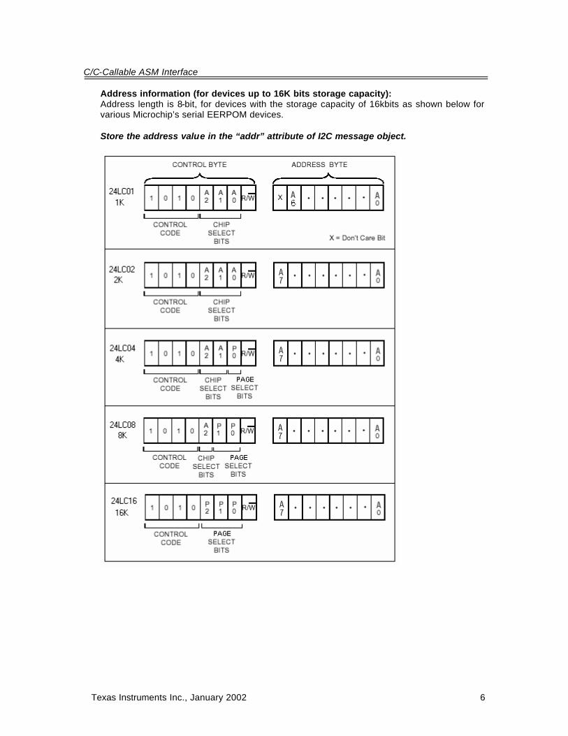
C/C-Callable ASM Interface
Address information (for devices up to 16K bits storage capacity): Address length is 8-bit, for devices with the storage capacity of 16kbits as shown below for various Microchip’s serial EERPOM devices. Store the address value in the “addr” attribute of I2C message object.

Texas Instruments Inc., January 2002 7
C/C-Callable ASM Interface
Address information (for devices above 16K bits storage capacity): Address length is two bytes for devices with the storage capacity of more then 16kbits as given below for various Microchip’s serial EERPOM devices. Store the address value in the “addr” attribute of I2C message object.
Address length selection
Edit the symbolic constant “ADDRWIDTH” in i2cse2p.h header file to select single byte addressing (for devices up to 16Kbits) or two-byte addressing (for devices above 16Kbits). Set the ADDRWIDTH symbolic constant to ONEBYTE for single byte addressing and to TWOBYTE for two-byte addressing.
/*******************************************************************/ /* Configurable Parameter for I2C bus Serial EEPROM */ /*******************************************************************/ #define ADDRWIDTH ONEBYTE /*******************************************************************/

Texas Instruments Inc., January 2002 8
C/C-Callable ASM Interface Serial EEPROM control and status register
WRITE REQ: Application program sets this bit after initializing the “msgPtr” element to perform the write operation.This bit is reset by write state machine after writing the data into serial EEPROM.
READ REQ: Application program sets this bit after initializing the “msgPtr” element to
perform the read operation. This bit is reset by read state machine after reading the data from serial EEPROM.
WRITE IN PROGRESS:
The serial EEPROM write state machine set this bit in the beginning of write operation and resets this bit along with the WRITE REQ bit after the write operation.
READ IN PROGRESS:
The serial EEPROM read state machine set this bit in the beginning of read operation and resets this bit along with the READ REQ bit after the read operation.
ERROR If acknowledge is not generated during the address or data transmit to serial
EEPROM , ERROR flag is set and exits the read or write operation. Application Program Interface (APIs) void init(I2CS E2P_IO *);
This function configures the I/O pins used for I2C bus serial clock (SCL) and serial data (SDA) in general purpose I/O mode and then as input. User can select I/O pins arbitrarily for serial clock (SCL) and serial data (SDA) by editing the following symbolic constants in i2cmpin.h file.
; I/O pin selection for SCL SCL_MUX .set GPFMUX SCL_DIR .set GPFDIR SCL_BIT .set BIT_2 ; I/O pin selection for SDA SDA_MUX .set GPFMUX SDA_DIR .set GPFDIR SDA_BIT .set BIT_1
1 0
RW-0 RW-0
3 2
RW-0 RW-0
READ IN
PROGRESS
WRITE IN
PROGRESS
READ
REQ
WRITE
REQ ERROR
4
RW-0

Texas Instruments Inc., January 2002 9
C/C-Callable ASM Interface void tick(I2CSE2P_IO *);
This function implements the read/write state machine of I2C bus serial EEPROM driver. Upon read/write request from application, it triggers the corresponding state sequence to carry out the request. The request bit (READ REQ or WRITE REQ) is reset at the end to indicate to the application that the request is fulfilled.
Serial EEPROM utilities unsigned int i2cSe2pFree(I2CSE2P_IO *);
This function checks the status of READ REQ & WRITE REQ bits (control and status register) and returns ONE if there were no request. It tells the application program that the driver is free and ready to accept the read or write request.
void i2cSe2pWrite(I2CSE2P_IO *, I2CSE2P_DATA *);
This function stores the message handle in the “msgPtr” element and asserts the write request by setting the csr.0 bit
void i2cSe2pRead(I2CSE2P_IO *, I2CSE2P_DATA *);
This function stores the message handle in the “msgPtr” element and asserts the read request by setting the csr.1 bit
Module Usage Instantiation The following example instances empty I2CSE2P_IO object I2CSE2P_IO se2p; Initialization To Instance pre-initialized object I2CSE2P_IO se2p= I2CSE2P_IO _DEFAULTS; Invoking the I2CSE2P_IO module API’s and Utilities se2p.init(&se2p); se2p.tick(&se2p); i2cSe2pFree(&se2p); i2cSe2pWrite(&se2p); i2cSe2pRead(&se2p); MIPS Requirement
The number cycles required to execute the tick function depends on the internal state of I2CSE2P_IO module. In worst case, the tick function takes 130 cycles to execute. The MIPS consumed by tick function depends on its invocation frequency.
Bit rate of I2C bus is ½ of the tick invocation frequency.
Assuming that the I2CSE2P_IO tick function is invoked in 20Khz ISR to perform data transfer @10kbps, then the MIPS consumed is given below
Maximum MIPS k20115×= = 2.3 MIPS

Texas Instruments Inc., January 2002 10
C/C-Callable ASM Interface Example
The pseudo code of I2CSE2P_IO driver module usage is given below Requirement specification: Interface the Microchip’s 32Kbits I2C Bus Serial EEPROM (24LC32B) to TI C2000 DSP.
1. The I/O pin requirement: SDA : PORT-F, BIT1 SCL : PORT-F, BIT2
2. Serial bit rate: 5Kbps Solution: Step 1: Edit the i2cmpin.h file to select the I/O pins for SDA and SCL signals.
Step 2: edit i2cse2p.h header file and specify the address width. Address width of 24LC32B device is 2 bytes.
Step 3: Rebuild the serial EEPROM driver library and add it to the project Step 4: Hardware setup: Connect the SDA and SCL pins of serial EEPROM to the I/O pins configured for SDA and SCL respectively. Select the device ID using A0, A1 & A2 pins. For example to select device ID ‘1’ (001), connect the A0 line to Vcc and A1 & A2 pins to ground for the device.
; I/O pin selection for SCL SCL_MUX .set GPFMUX SCL_DIR .set GPFDIR SCL_BIT .set BIT_2 ; I/O pin selection for SDA SDA_MUX .set GPFMUX SDA_DIR .set GPFDIR SDA_BIT .set BIT_1
/***********************************************************************/ /* Configurable Parameter for I2C bus Serial EEPROM */ /***********************************************************************/ #define ADDRWIDTH TWOBYTE /***********************************************************************/
C2000 DSP
SDA
SCL
R R
VCC
I/O
I/O
Serial
EEPROM
SDA
SCL
A0
A1
A2
VCC
Select the Device ID

Texas Instruments Inc., January 2002 11
C/C-Callable ASM Interface
Step 5: Invoke the serial EEPROM tick at twice the rate of the required bit rate. To transfer the data at 5kbps, invoke the tick function in 10khz timer ISR.
#include<i2cse2p.h> /* Instance the I2C bus serial EEPROM driver */
I2CSE2P_IO se2p= I2CSE2P_IO_DEFAULTS; /* Instance I2C serial EEPROM data transfer structure */
I2CSE2P_DATA writeData, readData; unsigned int writeBuf[10], readBuf[10], i, enable;
main( ) { /* initialize the VSPISE2P module */
se2p.init(&se2p); /* Initialise Write buff */ for(i=0;i<10;i++) writeBuf[i]=i; writeData.dataPtr=writeBuf; writeData.nrData=10; writeData.se2pAddr=0x00; writeData.Did_Blkr=0x1; /* Device ID: 1 */ readData.dataPtr=readBuf; readData.nrData=10; readData.se2pAddr=0x00; readData.Did_Blkr=0x1; /* Device ID: 1 */
/* Initialize timer to generate 10Khz Interrupt */
enable=1; /* Background loop */
while(1) { if(enable==1) {
/* Write into the serial EEPROM */ while(!i2cSe2pFree(&se2p)) i2cSe2pWrite(&se2p, &writeData); /* Read from serial EEPROM */ while(!i2cSe2pFree(&se2p)) i2cSe2pRead(&se2p, &readData); /* Wait for the driver to become free */ while(!i2cSe2pFree(&se2p)) enable=0
} }
} /* End: main() */

Texas Instruments Inc., January 2002 12
C/C-Callable ASM Interface
void interrupt isr10khz() {
/* Reset the interrupt flag */
/* Invoke Serial EEPROM driver tick */ se2p.tick(&se2p);
}

Texas Instruments Inc., January 2002 13
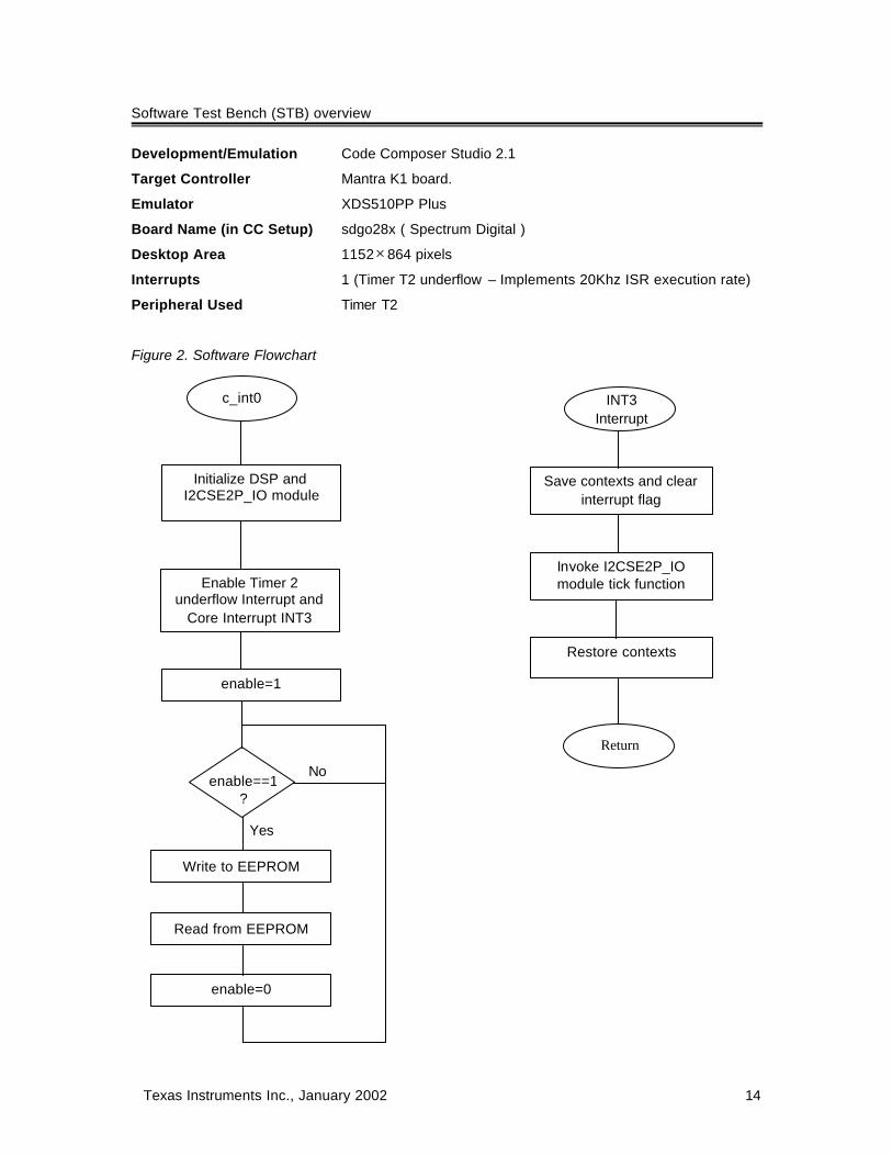
Chapter 2: Software Test Bench 1. Software Test Bench (STB) overview
This document describes the Software Test Bench (STB) to demonstrate the I2CSE2P_IO module implemented using C28x ISA. The software test bench is designed to run on Mantra K1 Board This test bench requires an I2C bus serial EEPROM device. It basically writes the data from write buffer into the I2C bus serial EEPROM starting at location 0x00, then reads back the same and stores the data in read buffer. Hence the user can quickly evaluate the working of the module by looking at the content of read buffer and write buffer.
Figure 1. Software Test Bench (STB) of I2CSE2P_IO module The STB for I2CSE2P_IO module has the following properties
C Frame work
System Name Program memory usage Data memory usage 1
I2CSE2P_IO 981 words 184 words
1 Excluding the Stack Size
I2CSE2P_IO
IOPF1/SPISOMI
IOPF2/SPICLK
R R
VCC
I2C Bus
Serial EEPROM
SDA
SCL
writeBuf[10]
readBuf[10]
Texas Instruments Inc., January 2002 14
Software Test Bench (STB) overview
Development/Emulation Code Composer Studio 2.1
Target Controller Mantra K1 board.
Emulator XDS510PP Plus
Board Name (in CC Setup) sdgo28x ( Spectrum Digital )
Desktop Area 1152× 864 pixels
Interrupts 1 (Timer T2 underflow – Implements 20Khz ISR execution rate)
Peripheral Used Timer T2
Figure 2. Software Flowchart
INT3 Interrupt
Save contexts and clear interrupt flag
Invoke I2CSE2P_IO module tick function
Return
Restore contexts
Initialize DSP and I2CSE2P_IO module
enable=1
c_int0
Enable Timer 2 underflow Interrupt and
Core Interrupt INT3
enable==1 ?
No
Yes
Write to EEPROM
Read from EEPROM
enable=0
Texas Instruments Inc., January 2002 15
Directory structure
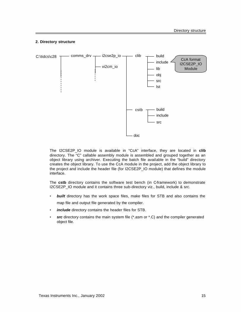
2. Directory structure
The I2CSE2P_IO module is available in “CcA” interface, they are located in clib directory. The “C” callable assembly module is assembled and grouped together as an object library using archiver. Executing the batch file available in the “build” directory creates the object library. To use the CcA module in the project, add the object library to the project and include the header file (for I2CSE2P_IO module) that defines the module interface.
The cstb directory contains the software test bench (in C-framework) to demonstrate I2CSE2P_IO module and it contains three sub-directory viz., build, include & src. • built directory has the work space files, make files for STB and also contains the
map file and output file generated by the compiler.
• include directory contains the header files for STB.
• src directory contains the main system file (*.asm or *.C) and the compiler generated object file.
C:\tidcs\c28 i2cse2p_io clib
build
include
lib
obj
src
lst
CcA format I2CSE2P_IO
Module
cstb build
include
src
doc
comms_drv
vi2cm_io

Texas Instruments Inc., January 2002 16
Hardware setup 3. Hardware Setup
Default pins configured for SDA and SCL signals are IOPE2/PWM8 and IOPE1/PWM7 respectively. Hence connect the SDA pin and SCL pin of serial EEPROM to IOPE2/PWM8 and IOPE1/PWM7 pin of DSP.
Figure 3. Hardware setup – F2812 ezDSP
Note: No need to connect A0, A1 & A2 pins to GND, if they are NC (Not connected) in the particular serial EEPOM device you are using. For example, in Microchip’s 24LC16B (8K) device A0, A1 & A2 are NC pins.
4. Address length selection
If the address length is one byte for the I2C serial EEPROM (for devices with storage capacity up to 16Kbits) then directly go to section 5 to execute the demo. For example following Microchip’s devices address length is one byte viz., 24LC01, 24LC02, 24LC04, 24LC08 and 24LC16. Otherwise (for devices with storage capacity greater then 16Kbits), configure the I2CSE2P_IO module for two-byte addressing and re-build the library. For example following Microchip’s devices address length is two bytes viz., 24LC32, 24LC64, 24LC128, 24LC256. a). Edit symbolic constant ADDRWIDTH in i2cse2p.h header file as given below (Full path: c:\ti\dcs\comms_drv\i2cse2p_io\clib\include\i2cse2p.h)
b) Execute build.bat file to re-build the library. (Full path name: c:\ti\dcs\comms_drv\i2cse2p_io\clib\\build\build.bat)
Mantra K1
IOPF1/SPISOMI
IOPF2/SPICLK
R R
I2C Bus Serial EEPROM
24LC16
SDA
SCL
GND GND
Vcc
P1(33)
JP13(2)
JP13(1) A0
A1
A2
/***********************************************************************/ /* Configurable Parameter for I2C bus Serial EEPROM */ /***********************************************************************/ #define ADDRWIDTH TWOBYTE /***********************************************************************/
Vcc
WP

Texas Instruments Inc., January 2002 17
Loading and building CC project 5. Loading and building CC project for I2CSE2P demo
The workspace file (*.wks) and make file (*.mak) for the STB is located within the build directory of cstb directory. The CC workspace file, contains the setup information for the whole project and the debugging environment such us the graph window properties, watch window parameters, break points and probe points etc. It facilitates the user to save and restore the same environment between debugging sessions instead of reconfiguring the working environment again and again for each debugging session. • To quickly execute demo using the pre-configured work environment, load the
workspace file “build.wks” from the build directory (Full path c:\c28x\dcs\comms_drv\i2cse2p_io\cstb\build\build.wks) Loading the workspace file will open up the project file (*.mak) for the corresponding project and show all the files relevant to the project in the FILEVIEW tab.
• From the Option menu choose ‘customize’ and enable the ‘Load Program After
Build’ option. This allows the automatic loading of the program to the target DSP once the program is compiled
• From the Project menu choose ‘Rebuild All’ or the ‘Rebuild All’ shortcut on the
toolbar to compile the program and load it to the target. Once this is done, the expanded project view as part of the CC environment will be as shown in figure 4. Memory window on the TOP shows the content of read buffer and memory window on the BOTTOM shows the content of write buffer. Upon power up these memory locations will have garbage data.
• Run the software by choosing Run from the Debug menu or using the tool bar
shortcut.
• Observe that the write and read buffer will have the same data as shown in figure 5, after it is halted due to breakpoint.

Texas Instruments Inc., January 2002 18
Loading and building CC project
Figure 4. CC Project view of I2CSE2P_IO demo
Figure 5. Run time view of I2CSE2P_IO demo