PCB VERIFICATION AND ORDERING
23
PCB VERIFICATION AND ORDERING George Hadley ©2016, Images Property of their Respective Owners.
Transcript of PCB VERIFICATION AND ORDERING

PCB VERIFICATION AND
ORDERING
George Hadley ©2016, Images Property of their Respective Owners.

OUTLINE• PCB Verification
• Parts Completion Check
• Footprint Verification Check
• Parts Placement Check
• Space Conflicts Check
• Routing Minimization Check
• Signal Plane Check
• Silkscreen Check
• Gerber File Generation
• PCB Ordering

PARTS COMPLETION CHECKValues and Ratings of Passive Components
• When choosing passive components, both component
value and power/voltage ratings matter
• Consider: How much current is running through your
resistors? How much voltage is being dropped across
your capacitors?Which of these resistor
packages is more likely to
survive having 4 amps run
through it?

PARTS COMPLETION CHECKMiscellaneous PCB Components
• Does your board have…
• A programming header? (note: use of an RJ-11
connector is not required)
• Reset tactile switch? (tact switches are recommended
over pushbuttons and other button types)
• A power connector and LED?
• Mounting holes?
• Debugging support?

FOOTPRINT VERIFICATION CHECK• Print a 1:1 scale layout of your board and lay your parts
on the printout to ensure that layout footprints match the
actual component packages
• Board doesn’t have
to be fully routed; what
matters is that you
have at least 1 instance
of every unique PCB
footprint on the printout
to compare against
physical parts

PARTS PLACEMENT CHECK• Is your crystal physically
close to your microcontroller?
• Are decoupling capacitors near/under microcontroller?
• Have connectors been placed at board edges?
• Are parts grouped by system or a logical order that minimizes trace lengths?

MECHANICAL CHECKX/Y-Space Conflicts
• Will your parts sit flush with the board? Has clearance
been provided for the X/Y space around your parts?
• For your mounting holes, has clearance been provided for
the heads of the bolts in addition to the bolt shaft?
• Best remedy to avoid these types of conflicts is to place
an outline of the part in the documentation layer

MECHANICAL CHECKZ-Space Conflicts
• When students add breakout boards, RPis/Atom Boards,
utilize stacked PCB design, or have special packaging
constraints, the height of components becomes
important. If components are too tall, they may run into
and/or create a short circuit with another board
• Best remedy to avoid these types of conflicts is to place
an outline of the part in the documentation layer (so you
know when to check for height concerns)
ROUTING CHECKSRouting Completion Check
• Have all airwires been resolved? (In Eagle, the ratsnest
command should report “Nothing to Do”)
• Have you separated AGND from GND using a jumper,
SMD resistor, or as suggested in your microcontroller
connection guidelines?

ROUTING CHECKSTrace Length Minimization Check
• Have unnecessary right angles been removed?
• Have PCB trace bends, loops, and spurs been removed?
(Loops function like antennae at high frequencies)
• Has octagonal
routing mode
been used?
(“Anything-goes”
diagonal routing
mode is not
recommended
for designs)

ROUTING CHECKSVia Minimization Check
• Have unnecessary vias been removed?
• Remember: you can enter through-hole pins from either
the top or bottom layers, just like vias
• Remember: you can route standard ~10 mil signal traces
between pairs of 0.1” spaced through-holes without
violating clearance requirements
• Remember: you can
route into a pin/pad
from any direction,
including behind it
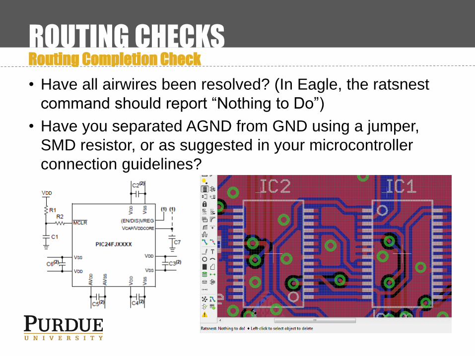
ROUTING CHECKSTrace/Via Current Capacity Check
• Have traces been sized appropriately to the amount of
current they are carrying? (32 mils or greater is
recommended for power traces; consult trace width
calculators for high current traces)
• Have vias in high-current traces been sized appropriately
to match the trace width?

SIGNAL PLANE CHECKS• Are signal planes being used
where appropriate?
• Has the isolation on all signal
planes been set to an
appropriate value? (Eagle
currently defaults isolation to
0; signal plane isolation of 12
mils or greater is STRONGLY
recommended).

SILKSCREEN CHECKS• Have labels been provided (in either the name or
silkscreen layers) for all component IDs and appropriate
connector signal names?
• Is pin 1 of all polarity-sensitive ICs and passives clearly
marked?
• Have all silkscreen labels been positioned so as to not
overlap pins, pads, or anywhere else that solder will be
applied?
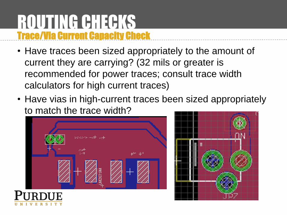
PCB LAYOUT IMPROVEMENTS• What’s good about this layout? What could be improved?

PCB LAYOUT IMPROVEMENTS• What’s good about this layout? What could be improved?

PCB LAYOUT IMPROVEMENTS• What’s good about this layout? What could be improved?

PCB LAYOUT IMPROVEMENTS• What’s good about this layout? What could be improved?

PCB LAYOUT IMPROVEMENTS• What’s good about this layout? What could be improved?

GERBER FILE GENERATION• Once PCB has been routed and passes DRC +
verification checks, the design must be translated into
machine files for PCB fabhouse equipment
• The current industry standard for PCB fabrication is the
Gerber RS274-X format (output option for Eagle, Altium,
etc.)
• In Eagle, CAM processor files are available on the course
website
(https://engineering.purdue.edu/ece477/Course/Process/
process.html)

GERBER FILE GENERATION• The CAM processor outputs a number of Gerber files:
• *.GTO (Top Overlay): Top silkscreen
• *.GTS (Top Soldermask): Top soldermask
• *.GTL (Top Layer): Top copper
• *.GBL (Bottom Layer): Bottom copper
• *.GBS (Bottom Soldermask): Bottom soldermask
• *.GBO (Bottom Overlay): Bottom silkscreen
• *.XLN (Excellon): Drill holes
• Once generated, inspect files with Gerber viewer (gerbv
recommended). When satisfied, zip files and send to
fabhouse

PCB ORDERING
• A few useful resources:
• OSH Park: US-based hobbyist service.
$5/square inch, 3 copies of each board design
• Advanced Circuits: US-based. $33 student
board special, quick turn times
• PCBShopper: PCB marketplace to compare
price quotes from 26 manufacturers instantly

Questions?


![Q5) 6LQJOH&KLS *+]5DGLR7UDQVFHLYHU Single chip 2.4 GHz ... · NRF2401 IC 24 pin QFN 5x5 A NRF2401-EVKIT Evaluation kit (2 test PCB, 2 configuration PCB, SW) 1.0 Table 2 nRF2401 ordering](https://static.fdocuments.in/doc/165x107/5e10fb92c143a17c360f11b5/q5-6lqjohkls-5dglr7udqvfhlyhu-single-chip-24-ghz-nrf2401-ic-24-pin.jpg)