MONOBLOC INSTRUCTION MANUAL diagrams only€¦ · 4700uF 16V PCB Pin 7, 450V PCB Pin 2 PCB Pin 6...
6
KEL80 MONOBLOC INSTRUCTION MANUAL diagrams only
Transcript of MONOBLOC INSTRUCTION MANUAL diagrams only€¦ · 4700uF 16V PCB Pin 7, 450V PCB Pin 2 PCB Pin 6...
KEL80MONOBLOC
INSTRUCTIONMANUAL
diagrams only
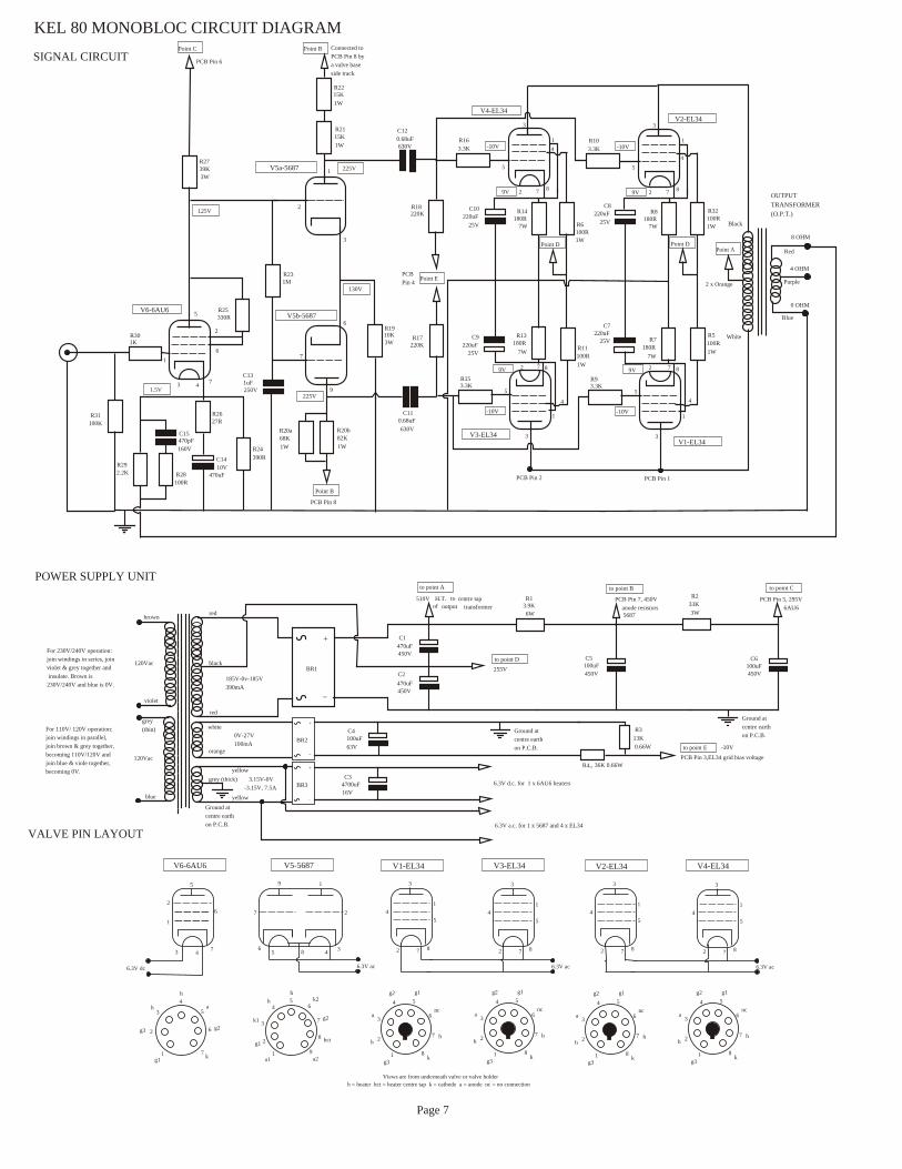
V5-5687
V5a-5687
V5b-5687
V1-EL34 V2-EL34V3-EL34 V4-EL34
100K
1K
27R
330R
39K3W
1M
1W
1W
15K
15K
1W1W
10K
220K
220K3W
82K68K
3.3K 3.3K
3.3K 3.3K
2.2K
1W1W
100R100R 1W1W
180R 180R7W 7W
180R 180R7W 7W
470uF10V
1uF250V
220uF 220uF25V 25V
220uF220uF
25V25V
0.68uF630V
0.68uF630V
0 OHM
8 OHM
4 OHM
OUTPUTTRANSFORMER(O.P.T.)
1
2
5
5
6
7
1
2
9
7
6
3
7
7 7
3
3
4
4
1 1
2 2
3 3
44
5 5
8 8
1 1
2 2
3 3
4 45 5
7 78 8
26
1
12
3
45 6
7
8
91
2
34
5
6
7
1
2
3456
7
8
9
1 11 1
2 22 2
3 33 3
4 44 45 55 5
7 77 78 88 8
1 11 1
2 22 2
3 33 3
4 44 45 55 5
6 66 6
7 77 7
8 88 8
a
kg1
g2g3
h
h
a1
k2
k1
hctg1
g2
hh
a2
a aa a
k kk k
g1 g1g1 g1g2 g2g2 g2
g3 g3g3 g3
h hh hh hh h
nc ncnc nc
V6-6AU6
6.3V dc 6.3V ac6.3V ac 6.3V ac
Views are from underneath valve or valve holderh = heater hct = heater centre tap k = cathode a = anode nc = no connection
100R100R
Point E
Point APoint D Point D
Point BPoint C
Point B
VALVE PIN LAYOUT
Page 7
470pF160V
+
+
+
_
_
_
BR1
BR2
BR3
470uF
470uF
450V
450V
100uF450V
100uF450V
6.3V d.c. for 1 x 6AU6 heaters
6.3V a.c. for 1 x 5687 and 4 x EL34
PCB Pin 3,EL34 grid bias voltage
100uF63V
4700uF16V
PCB Pin 7, 450V
PCB Pin 2
PCB Pin 6
PCB Pin 8
Connected toPCB Pin 8 bya valve base side track
PCB Pin 4
PCB Pin 1
5687
PCB Pin 5, 295V6AU6
510V H.T. to centre tapof output transformer
Ground atcentre earthon P.C.B.
Ground atcentre earthon P.C.B.
Ground atcentre earthon P.C.B.
to point D
to point A to point B to point C
to point E
33K3W
3.9K6W
POWER SUPPLY UNIT
anode resistors
255V 120Vac
120Vac
185V-0v-185V390mA
3.15V-0V-3.15V, 7.5A
R1
R3
R2
R4,
-10V
C1
C2
C3
C4
C5 C6
, 36K 0.66W
13K 0.66W
R30
R26
R24
R27
R23
R21
R22
R20bR20a
R19
R18
R17
R16 R10
R15 R9
R32
2 x Orange
Black
White
Blue
Purple
Red
R6
R5R11
R31
R25
R14 R8
R13 R7
R29
C15
C10 C8
C9C7
C12
C11
C14
C13
225V
225V
125V
130V
1.5V
-10V -10V
-10V -10V
9V 9V
9V 9V
0V-27V100mA
For 230V/240V operation:join windings in series, joinviolet & grey together and insulate. Brown is230V/240V and blue is 0V.
For 110V/ 120V operation:join windings in parallel,join brown & grey together,becoming 110V/120V andjoin blue & viole together,becoming 0V.
V6-6AU6
V4-EL34V2-EL34
V3-EL34 V1-EL34
red
red
black
white
yellow
yellow
grey (thick)
orange
brown
blue
grey(thin)
violet
SIGNAL CIRCUIT
KEL 80 MONOBLOC CIRCUIT DIAGRAM
100R
390R
R28
tab 1tab 2
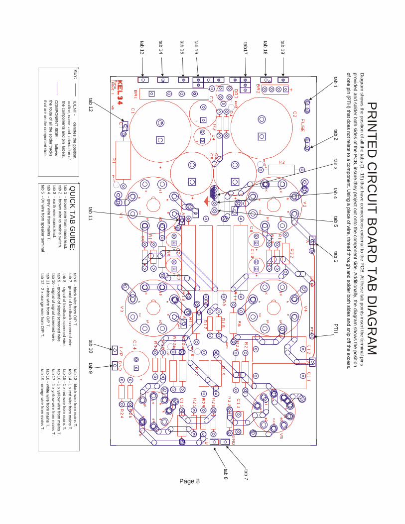
tab 1 - brown wire from mains lead.tab 2 - brown wire to mains switch.tab 3 - earth wire mains lead.tab 4 - grey wire from mains T.
QUICK TAB GUIDE:
tab 5 - 0V wire from speaker terminal
tab 6 - black wire from O/P T.
tab 10 - signal of signal screened wire.tab 11 - white wire from O/P T.tab 12 - 2 x orange wire from O/P T.
tab 3tab 4
tab 5tab 6
tab 7
PTH
tab 8
tab 9tab 10
tab 11tab 12
tab 13
tab 14
tab 15
tab 16
tab17
tab 18
tab 19
tab 15 - 1 x red wire from mains T.tab 16 - 1 x yellow wire from mains T.tab 17 - 1 x yellow wire from mains T.tab 18 - white wire from mains T.tab 19 - orange wire from mains T.
IDENT - denotes the position, outline, name and orientation of the components and pin labels. COMPONENT SIDE - followsthe route of all the solder tracksthat are on the component side.
KEY:
Diagram shows the position of all the tabs (1 - 19) that have connections external to the PCB. At these tab points insert the terminal pins provided and solder both sides of the PCB, insure they project out onto the component side. Additionally, the diagram shows the position of one pin (PTH) that does not relate to a component. Using a piece of wire, thread through and solder both sides and snip off the excess.
PRINTED CIRCUIT BOARD TAB DIAGRAM
tab 8 - signal of feedback screened wire.tab 7 - ground of feedback screened wire
tab 14 - 1 x red wire from mains T. tab 13 - black wire from mains T.
tab 14 - 1 x red wire from mains T.
tab 9 - ground of signal screened wire.
Page 8
Heater link 1
Heater link 2
link 2
link 4
link 1
link 3
Heater link 5
Heater link 6
Heater link 7
Heater link 8
Heater link 9
Heater link 10
Heater link 11
Heater link 12
Heater link 3
Heater link 4
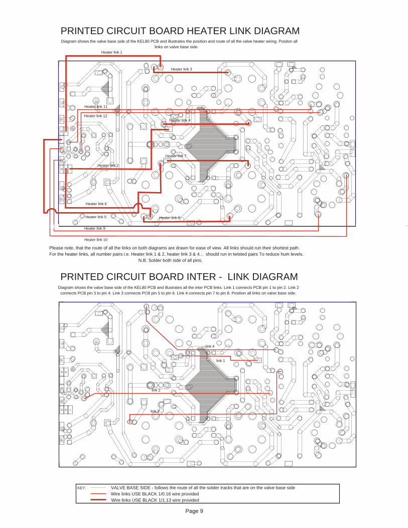
PRINTED CIRCUIT BOARD HEATER LINK DIAGRAM
PRINTED CIRCUIT BOARD INTER - LINK DIAGRAM
VALVE BASE SIDE - follows the route of all the solder tracks that are on the valve base sideWire links USE BLACK 1/0.16 wire providedWire links USE BLACK 1/1.13 wire provided
KEY:
Please note, that the route of all the links on both diagrams are drawn for ease of view. All links should run their shortest path. For the heater links, all number pairs i.e. Heater link 1 & 2, heater link 3 & 4... should run in twisted pairs To reduce hum levels. N.B. Solder both side of all pins.
Diagram shows the valve base side of the KEL80 PCB and illustrates all the inter PCB links. Link 1 connects PCB pin 1 to pin 2. Link 2 connects PCB pin 3 to pin 4. Link 3 connects PCB pin 5 to pin 6. Link 4 connects pin 7 to pin 8. Position all links on valve base side.
Diagram shows the valve base side of the KEL80 PCB and illustrates the position and route of all the valve heater wiring. Positon all links on valve base side.
Page 9
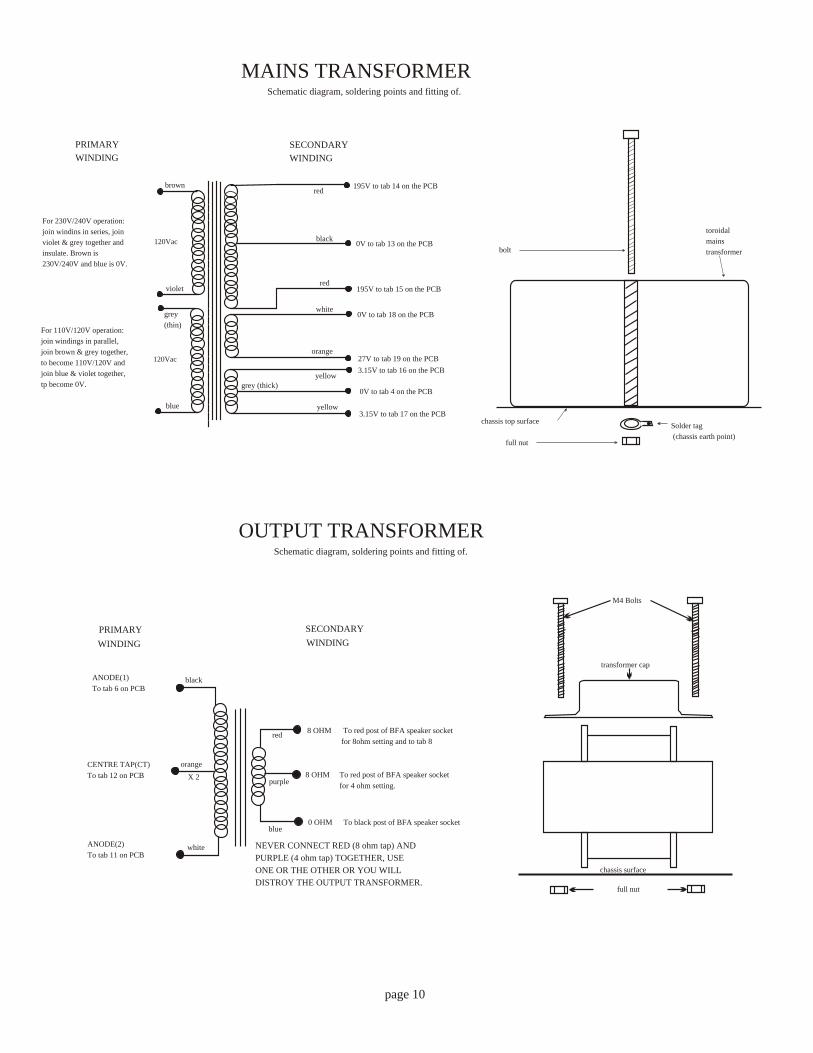
0 OHM
8 OHM
8 OHM
blue
purple
red
OUTPUT TRANSFORMER
black
orangeX 2
ANODE(1)To tab 6 on PCB
ANODE(2)To tab 11 on PCB
CENTRE TAP(CT) To tab 12 on PCB
PRIMARY SECONDARYWINDINGWINDING
To red post of BFA speaker socket for 8ohm setting and to tab 8
To red post of BFA speaker socket for 4 ohm setting.
NEVER CONNECT RED (8 ohm tap) ANDPURPLE (4 ohm tap) TOGETHER, USE ONE OR THE OTHER OR YOU WILL DISTROY THE OUTPUT TRANSFORMER.
To black post of BFA speaker socket
Schematic diagram, soldering points and fitting of.
120Vac
120Vac
For 230V/240V operation:join windins in series, joinviolet & grey together andinsulate. Brown is 230V/240V and blue is 0V.
For 110V/120V operation:join windings in parallel,join brown & grey together,to become 110V/120V and join blue & violet together,tp become 0V.
195V to tab 14 on the PCB
195V to tab 15 on the PCB
0V to tab 13 on the PCB
0V to tab 18 on the PCB
27V to tab 19 on the PCB 3.15V to tab 16 on the PCB
0V to tab 4 on the PCB
3.15V to tab 17 on the PCB
red
black
red
white
orange
yellowgrey (thick)
yellowblue
grey(thin)
violet
brown
MAINS TRANSFORMER
PRIMARYWINDING
SECONDARY WINDING
Schematic diagram, soldering points and fitting of.
full nut
full nut
Solder tag (chassis earth point)
chassis top surface
bolt
toroidalmains transformer
white
page 10
M4 Bolts
transformer cap
chassis surface
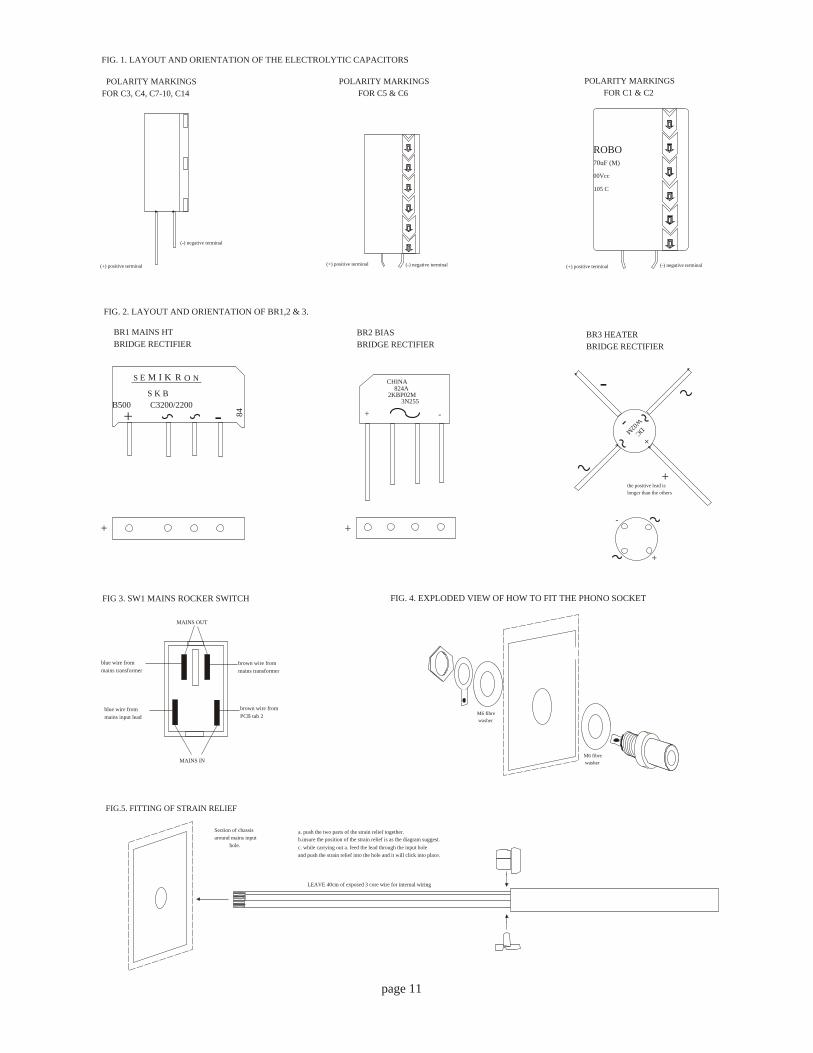
BR1 MAINS HT BRIDGE RECTIFIER
BR3 HEATER BRIDGE RECTIFIER
+
+ +
+
+
+
+
-
-
---
BR2 BIAS BRIDGE RECTIFIER
S E M I K R O N
B500 C3200/2200S K B
84
CHINA824A
2KBP02M3N255
DCW02M
the positive lead is longer than the others
M6 fibre washer
M6 fibre washer
ROBO70uF (M)00Vcc105 C
(-) negative terminal(-) negative terminal
(-) negative terminal
(+) positive terminal(+) positive terminal (+) positive terminal
POLARITY MARKINGS FOR C1 & C2
POLARITY MARKINGS FOR C5 & C6
POLARITY MARKINGS FOR C3, C4, C7-10, C14
FIG 3. SW1 MAINS ROCKER SWITCH
MAINS IN
MAINS OUT
FIG. 2. LAYOUT AND ORIENTATION OF BR1,2 & 3.
FIG. 1. LAYOUT AND ORIENTATION OF THE ELECTROLYTIC CAPACITORS
blue wire frommains transformer
blue wire frommains input lead
brown wire frommains transformer
brown wire from PCB tab 2
CDInput
FIG. 4. EXPLODED VIEW OF HOW TO FIT THE PHONO SOCKET
LEAVE 40cm of exposed 3 core wire for internal wiring
Section of chassisaround mains input hole.
a. push the two parts of the strain relief together.
c. while carrying out a. feed the lead through the input holeand push the strain relief into the hole and it will click into place.
b.insure the position of the strain relief is as the diagram suggest.
FIG.5. FITTING OF STRAIN RELIEF
page 11


![Q5) 6LQJOH&KLS *+]5DGLR7UDQVFHLYHU Single chip 2.4 GHz ... · NRF2401 IC 24 pin QFN 5x5 A NRF2401-EVKIT Evaluation kit (2 test PCB, 2 configuration PCB, SW) 1.0 Table 2 nRF2401 ordering](https://static.fdocuments.in/doc/165x107/5e10fb92c143a17c360f11b5/q5-6lqjohkls-5dglr7udqvfhlyhu-single-chip-24-ghz-nrf2401-ic-24-pin.jpg)