PB-MC-AVR28 28 Pin AVR Full Size Development Board · 2019-01-25 · PB-MC-AVR28 28 Pin AVR Full...
20
PB-MC-AVR28 28 Pin AVR Full Size Development Board User Guide Version 1.0 14 September 2008 PB-MC-AVR28-UG
Transcript of PB-MC-AVR28 28 Pin AVR Full Size Development Board · 2019-01-25 · PB-MC-AVR28 28 Pin AVR Full...

PB-MC-AVR28 28 Pin AVR Full Size Development Board
User Guide
Version 1.0 14 September 2008
PB-MC-AVR28-UG

PB-MC-AVR28 28 Pin AVR Full Size Development Board User Guide Version 1.0
14 September 2008
iii
TABLE OF CONTENTS
1. OVERVIEW .......................................................................................................................... 1
1.1. Introduction ............................................................................................................. 1
1.2. References .............................................................................................................. 1 1.2.1. Referenced Documents .................................................................................... 1 1.2.2. Acronyms and Abbreviations ............................................................................ 1 1.2.3. Definitions ........................................................................................................ 2
1.3. Supported Microcontrollers ...................................................................................... 2
1.4. Warnings ................................................................................................................. 2
2. BOARD LAYOUT .................................................................................................................. 3
2.1. Microcontroller ......................................................................................................... 4
2.2. Pull-up resistor and Reset Button ............................................................................ 4
2.3. ISP Port ................................................................................................................... 5
2.4. AVCC Block............................................................................................................. 5
2.5. External Oscillator ................................................................................................... 6
2.6. Ports PD0-PD7, PB0-PB7 and PC0-PC6 ................................................................. 6
2.7. Positive and Ground power rails .............................................................................. 7
2.8. 3 hole I/O Protostrips ............................................................................................... 8
2.9. Small and large prototyping areas ........................................................................... 9 2.9.1. Using the prototyping area to interface to the board ......................................... 9
2.10. Mounting Holes ..................................................................................................... 10
3. BOARD SETUP .................................................................................................................. 11
3.1. Attach the microcontroller ...................................................................................... 11
3.2. Add the pull-up resistor and reset switch ............................................................... 12
3.3. Add the ISP Connector .......................................................................................... 13
3.4. Wire up the AVCC Block ....................................................................................... 14
3.5. Add an external Oscillator...................................................................................... 15
3.6. Add a power source ............................................................................................... 15
3.7. Add some I/O ........................................................................................................ 15
4. COMMENT AND QUESTIONS ............................................................................................... 16
PB-MC-AVR28 28 Pin AVR Full Size Development Board User Guide Version 1.0
14 September 2008
iv
TABLE OF TABLES
Table 1. Referenced Documents ........................................................................................................... 1Table 2. Acronyms and Abbreviations ................................................................................................... 1Table 3. Definitions ................................................................................................................................ 2Table 4. Supported Microcontrollers ...................................................................................................... 2Table 5. Data Port Mappings ................................................................................................................. 7
TABLE OF FIGURES
Figure 1. Board layout – AVR Specific features ...................................................................................... 3Figure 2. Board layout – General Specific features ................................................................................ 4Figure 3. Microcontroller location on Board ............................................................................................ 4Figure 4. Pull-up resistor and reset switch ............................................................................................... 5Figure 5. ISP port pinout ......................................................................................................................... 5Figure 6. AVCC Low Pass Filter ............................................................................................................. 6Figure 7. Positive and ground power rails ............................................................................................... 8Figure 8. Stacking headers used in a 3 board stack ............................................................................... 8Figure 9. Polarised header used in 3 hole protostrips ............................................................................ 9Figure 10. Prototyping areas ................................................................................................................... 9Figure 11. Right angle polarised header on board ............................................................................... 10Figure 12. Microcontroller markings and orientation ............................................................................. 11Figure 13. Microcontroller location on board ......................................................................................... 11Figure 14. IC Socket on board .............................................................................................................. 12Figure 15. Microcontroller in socket ...................................................................................................... 12Figure 16. 10KΩ pull-up resistor for reset (pin 1) ................................................................................... 12Figure 17. Pin pairs on micro tactile switch ............................................................................................ 13Figure 18. Reset button on board ......................................................................................................... 13Figure 19. ISP Right Angle Connector .................................................................................................. 14Figure 20. ISP Straight Pin Connector .................................................................................................. 14Figure 21. AVCC Connected to VCC with Jumper ............................................................................... 14Figure 22. External Oscillator on board ................................................................................................ 15

PB-MC-AVR28 28 Pin AVR Full Size Development Board User Guide Version 1.0
14 September 2008
1
1. Overview
1.1. Introduction
The Protostack 28 Pin AVR Full Size Development Board is designed for ATMEL AVR Microcontrollers that are available in the PDIP 28 pin package. This board performs the following functions:
a. Provides the infrastructure necessary to use the microcontroller,
b. “Untangles” the I/O ports in order to present them in an orderly fashion, and
c. Provides area for the user to add their own circuitry
This board conforms to the Protostack full size board form factor and is able to be stacked with other full size or half size boards.
1.2. References
1.2.1. Referenced Documents
The documents referenced in this User Guide are listed in Table 1.
Document Version Date PB-MC-AVR28 Datasheet tba tba AT90S2333/AT90LS2333/AT90S4433/AT90LS4433 Datasheet
1042DS–04/99 N/A
ATmega8/ ATmega8L Datasheet 2486S–AVR–08/07 N/A ATmega48/V, ATmega88/V and ATmega168/V Datasheet 2545M–AVR–09/07 N/A
Table 1. Referenced Documents
1.2.2. Acronyms and Abbreviations
The acronyms and abbreviations utilised in this User Guide are listed in Table 2.
Acronym and Abbreviation Description AVCC Analogue VCC AVR Advanced Virtual RISC DIP Dual Inline Package IC Integrated Circuit I/O Input/Output ISP In System/Service Programming PDIP Plastic Dual Inline Package VCC Positive supply voltage
Table 2. Acronyms and Abbreviations
PB-MC-AVR28 28 Pin AVR Full Size Development Board User Guide Version 1.0
14 September 2008
2
1.2.3. Definitions
The definitions utilised in this User Guide are listed in Table 3.
Term Definition Firmware Firmware is a software program or set of instructions programmed onto
the microcontroller. It provides the necessary instructions for how the device communicates with the other hardware.
Flash Non-volatile computer memory that can be electrically erased and reprogrammed
Protostrip A strip of 2 or more holes (pad) on a prototyping board that are connected together
Table 3. Definitions
1.3. Supported Microcontrollers
Table 4 lists the microcontrollers that are supported by the 28 Pin AVR Full Size Development Board.
Microcontroller Flash EPROM SRAM Speed Notes AT90S2333 2 Kbytes 128 Bytes 128 Bytes 0-8 MHz Obsolete AT90LS2333 2 Kbytes 128 Bytes 128 Bytes 0-4 MHz Obsolete AT90S4433 4 Kbytes 256 Bytes 128 Bytes 0-8 MHz Obsolete AT90LS4433 4 Kbytes 256 Bytes 128 Bytes 0-4 MHz Obsolete ATMEGA8 8 Kbytes 512 Bytes 1 Kbytes 0-16 MHz ATMEGA8L 8 Kbytes 512 Bytes 1 Kbytes 0-8 MHz ATMEGA48 4 Kbytes 256 Bytes 512 Bytes 0-20 MHz ATMEGA48V 4 Kbytes 256 Bytes 512 Bytes 0-10 MHz ATMEGA88 8 Kbytes 512 Bytes 1 Kbytes 0-20 MHz ATMEGA88V 8 Kbytes 512 Bytes 1 Kbytes 0-10 MHz ATMEGA168 16 Kbytes 512 Bytes 1 Kbytes 0-20 MHz ATMEGA168V 16 Kbytes 512 Bytes 1 Kbytes 0-10 MHz
Table 4. Supported Microcontrollers
1.4. Warnings
Some of the components discussed in this document are very sensitive to electrical static discharges. The reader should take precautions to ensure that components are protected against these discharges.
Whilst the voltages typically seen in microcontroller circuits are low, the reader should be aware of the risk of working with electrical circuits and take necessary precautions.
PB-MC-AVR28 28 Pin AVR Full Size Development Board User Guide Version 1.0
14 September 2008
3
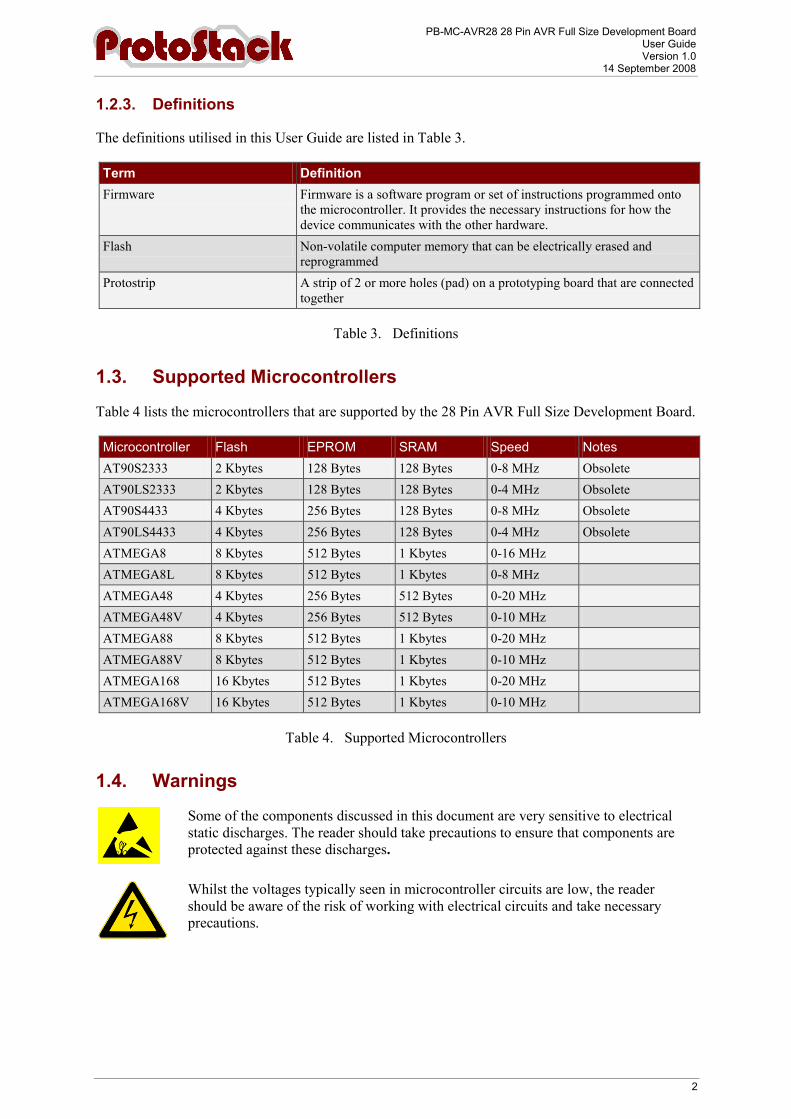
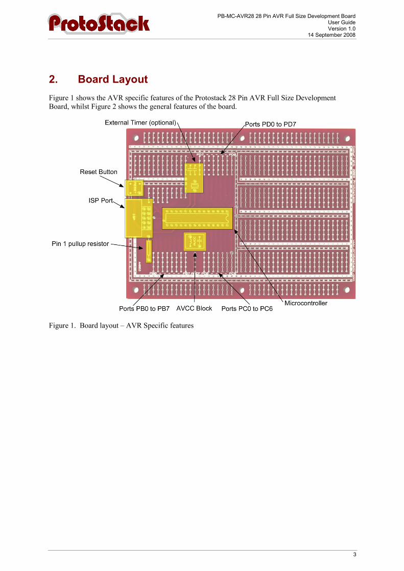
2. Board Layout Figure 1 shows the AVR specific features of the Protostack 28 Pin AVR Full Size Development Board, whilst Figure 2 shows the general features of the board.
Figure 1. Board layout – AVR Specific features
PB-MC-AVR28 28 Pin AVR Full Size Development Board User Guide Version 1.0
14 September 2008
4
Figure 2. Board layout – General Specific features
2.1. Microcontroller
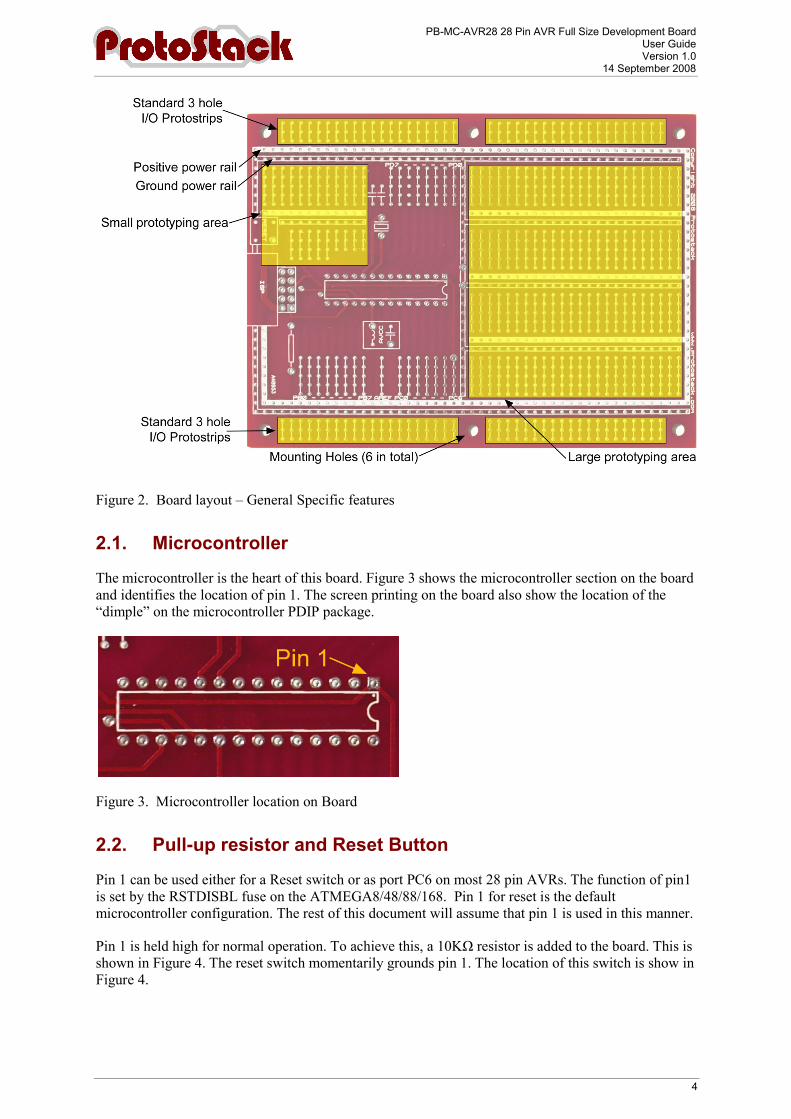
The microcontroller is the heart of this board. Figure 3 shows the microcontroller section on the board and identifies the location of pin 1. The screen printing on the board also show the location of the “dimple” on the microcontroller PDIP package.
Figure 3. Microcontroller location on Board
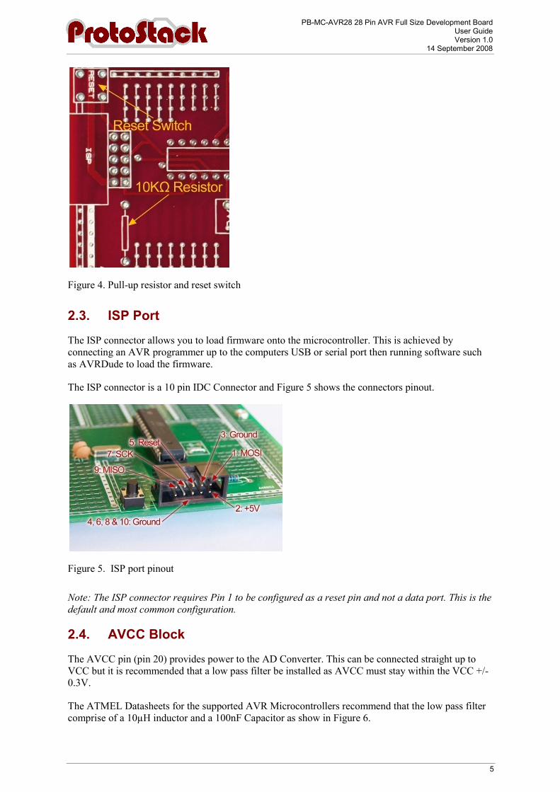
2.2. Pull-up resistor and Reset Button
Pin 1 can be used either for a Reset switch or as port PC6 on most 28 pin AVRs. The function of pin1 is set by the RSTDISBL fuse on the ATMEGA8/48/88/168. Pin 1 for reset is the default microcontroller configuration. The rest of this document will assume that pin 1 is used in this manner.
Pin 1 is held high for normal operation. To achieve this, a 10KΩ resistor is added to the board. This is shown in Figure 4. The reset switch momentarily grounds pin 1. The location of this switch is show in Figure 4.
PB-MC-AVR28 28 Pin AVR Full Size Development Board User Guide Version 1.0
14 September 2008
5
Figure 4. Pull-up resistor and reset switch
2.3. ISP Port
The ISP connector allows you to load firmware onto the microcontroller. This is achieved by connecting an AVR programmer up to the computers USB or serial port then running software such as AVRDude to load the firmware.
The ISP connector is a 10 pin IDC Connector and Figure 5 shows the connectors pinout.
Figure 5. ISP port pinout
Note: The ISP connector requires Pin 1 to be configured as a reset pin and not a data port. This is the default and most common configuration.
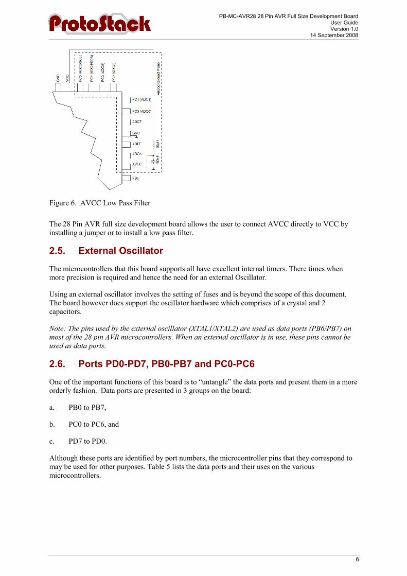
2.4. AVCC Block
The AVCC pin (pin 20) provides power to the AD Converter. This can be connected straight up to VCC but it is recommended that a low pass filter be installed as AVCC must stay within the VCC +/- 0.3V.
The ATMEL Datasheets for the supported AVR Microcontrollers recommend that the low pass filter comprise of a 10µH inductor and a 100nF Capacitor as show in Figure 6.
PB-MC-AVR28 28 Pin AVR Full Size Development Board User Guide Version 1.0
14 September 2008
6
Figure 6. AVCC Low Pass Filter
The 28 Pin AVR full size development board allows the user to connect AVCC directly to VCC by installing a jumper or to install a low pass filter.
2.5. External Oscillator
The microcontrollers that this board supports all have excellent internal timers. There times when more precision is required and hence the need for an external Oscillator.
Using an external oscillator involves the setting of fuses and is beyond the scope of this document. The board however does support the oscillator hardware which comprises of a crystal and 2 capacitors.
Note: The pins used by the external oscillator (XTAL1/XTAL2) are used as data ports (PB6/PB7) on most of the 28 pin AVR microcontrollers. When an external oscillator is in use, these pins cannot be used as data ports.
2.6. Ports PD0-PD7, PB0-PB7 and PC0-PC6
One of the important functions of this board is to “untangle” the data ports and present them in a more orderly fashion. Data ports are presented in 3 groups on the board:
a. PB0 to PB7,
b. PC0 to PC6, and
c. PD7 to PD0.
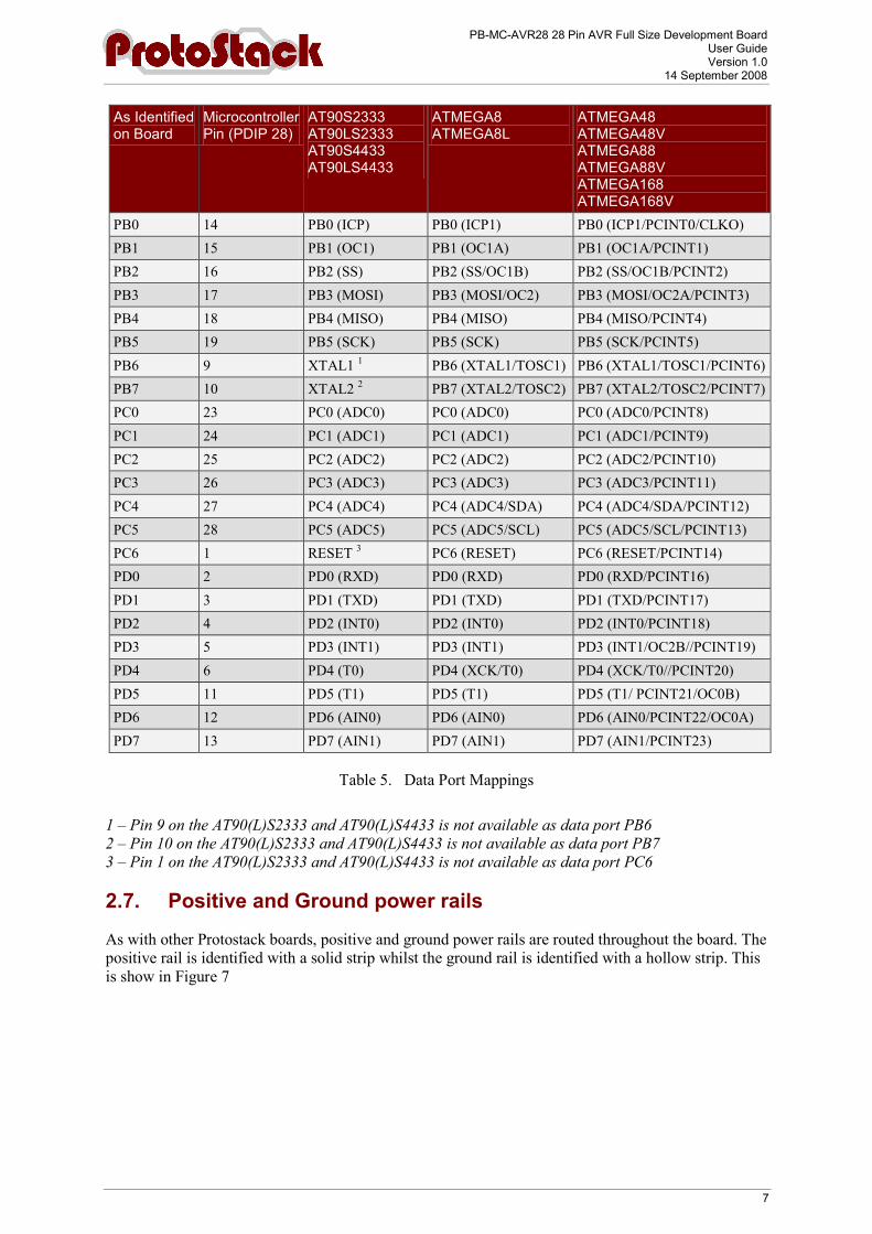
Although these ports are identified by port numbers, the microcontroller pins that they correspond to may be used for other purposes. Table 5 lists the data ports and their uses on the various microcontrollers.
PB-MC-AVR28 28 Pin AVR Full Size Development Board User Guide Version 1.0
14 September 2008
7
As Identified on Board
Microcontroller Pin (PDIP 28)
AT90S2333 AT90LS2333 AT90S4433 AT90LS4433
ATMEGA8 ATMEGA8L
ATMEGA48 ATMEGA48V ATMEGA88 ATMEGA88V ATMEGA168 ATMEGA168V
PB0 14 PB0 (ICP) PB0 (ICP1) PB0 (ICP1/PCINT0/CLKO) PB1 15 PB1 (OC1) PB1 (OC1A) PB1 (OC1A/PCINT1) PB2 16 PB2 (SS) PB2 (SS/OC1B) PB2 (SS/OC1B/PCINT2) PB3 17 PB3 (MOSI) PB3 (MOSI/OC2) PB3 (MOSI/OC2A/PCINT3) PB4 18 PB4 (MISO) PB4 (MISO) PB4 (MISO/PCINT4) PB5 19 PB5 (SCK) PB5 (SCK) PB5 (SCK/PCINT5) PB6 9 XTAL1 1 PB6 (XTAL1/TOSC1) PB6 (XTAL1/TOSC1/PCINT6) PB7 10 XTAL2 2 PB7 (XTAL2/TOSC2) PB7 (XTAL2/TOSC2/PCINT7) PC0 23 PC0 (ADC0) PC0 (ADC0) PC0 (ADC0/PCINT8) PC1 24 PC1 (ADC1) PC1 (ADC1) PC1 (ADC1/PCINT9) PC2 25 PC2 (ADC2) PC2 (ADC2) PC2 (ADC2/PCINT10) PC3 26 PC3 (ADC3) PC3 (ADC3) PC3 (ADC3/PCINT11) PC4 27 PC4 (ADC4) PC4 (ADC4/SDA) PC4 (ADC4/SDA/PCINT12) PC5 28 PC5 (ADC5) PC5 (ADC5/SCL) PC5 (ADC5/SCL/PCINT13) PC6 1 RESET 3 PC6 (RESET) PC6 (RESET/PCINT14) PD0 2 PD0 (RXD) PD0 (RXD) PD0 (RXD/PCINT16) PD1 3 PD1 (TXD) PD1 (TXD) PD1 (TXD/PCINT17) PD2 4 PD2 (INT0) PD2 (INT0) PD2 (INT0/PCINT18) PD3 5 PD3 (INT1) PD3 (INT1) PD3 (INT1/OC2B//PCINT19) PD4 6 PD4 (T0) PD4 (XCK/T0) PD4 (XCK/T0//PCINT20) PD5 11 PD5 (T1) PD5 (T1) PD5 (T1/ PCINT21/OC0B) PD6 12 PD6 (AIN0) PD6 (AIN0) PD6 (AIN0/PCINT22/OC0A) PD7 13 PD7 (AIN1) PD7 (AIN1) PD7 (AIN1/PCINT23)
Table 5. Data Port Mappings
1 – Pin 9 on the AT90(L)S2333 and AT90(L)S4433 is not available as data port PB6 2 – Pin 10 on the AT90(L)S2333 and AT90(L)S4433 is not available as data port PB7 3 – Pin 1 on the AT90(L)S2333 and AT90(L)S4433 is not available as data port PC6
2.7. Positive and Ground power rails
As with other Protostack boards, positive and ground power rails are routed throughout the board. The positive rail is identified with a solid strip whilst the ground rail is identified with a hollow strip. This is show in Figure 7
PB-MC-AVR28 28 Pin AVR Full Size Development Board User Guide Version 1.0
14 September 2008
8
Figure 7. Positive and ground power rails
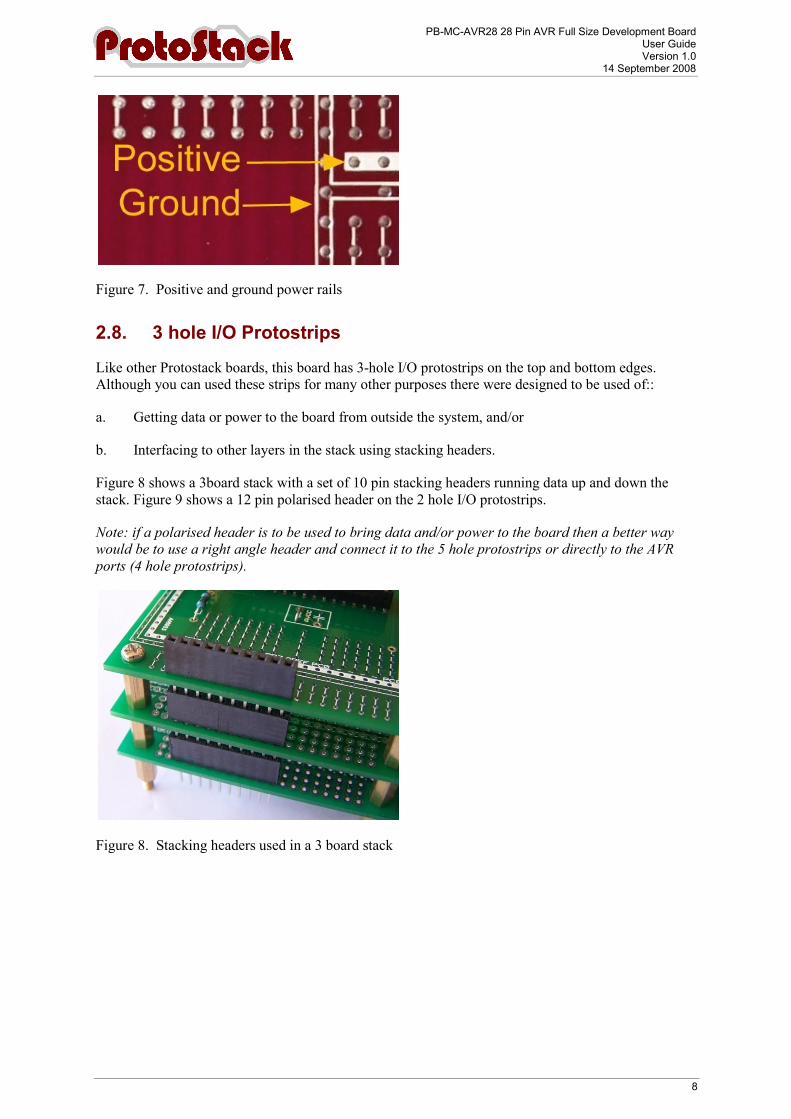
2.8. 3 hole I/O Protostrips
Like other Protostack boards, this board has 3-hole I/O protostrips on the top and bottom edges. Although you can used these strips for many other purposes there were designed to be used of::
a. Getting data or power to the board from outside the system, and/or
b. Interfacing to other layers in the stack using stacking headers.
Figure 8 shows a 3board stack with a set of 10 pin stacking headers running data up and down the stack. Figure 9 shows a 12 pin polarised header on the 2 hole I/O protostrips.
Note: if a polarised header is to be used to bring data and/or power to the board then a better way would be to use a right angle header and connect it to the 5 hole protostrips or directly to the AVR ports (4 hole protostrips).
Figure 8. Stacking headers used in a 3 board stack

PB-MC-AVR28 28 Pin AVR Full Size Development Board User Guide Version 1.0
14 September 2008
9
Figure 9. Polarised header used in 3 hole protostrips
2.9. Small and large prototyping areas
The prototyping areas are based on the layout of a breadboard and consist of:
a. Positive Power Rail,
b. Ground power rail, and
c. A number of 5-hole protostrips arranged parallel to each other.
This is shown in Figure 10.
Figure 10. Prototyping areas
2.9.1. Using the prototyping area to interface to the board
In general the 3 hole I/O protostrips on the top and bottom of the board are used for interfacing between boards in a stack or to the outside world. A useful exception is the use of right angled polarised headers directly.

PB-MC-AVR28 28 Pin AVR Full Size Development Board User Guide Version 1.0
14 September 2008
10
Figure 11. Right angle polarised header on board
2.10. Mounting Holes
This board conforms to the standard form factor for full size protostack boards. This includes 6 mounting holes which can be used for stacking boards together with hexagonal spacers and/or mounting the boards to a faceplate or case.

PB-MC-AVR28 28 Pin AVR Full Size Development Board User Guide Version 1.0
14 September 2008
11
3. Board Setup This section describes the process involved to get your board operational.
3.1. Attach the microcontroller
Like most ICs using a PDIP package, the AMTEL AVR series of Microcontrollers has a small dimple on one end showing you how to orient the chip and the location of pin 1. Figure 12 shows the location of the dimple and pin 1.
Figure 12. Microcontroller markings and orientation
To make IC orientation easier, a white outline on the board shows the location of the dimple and pin 1 is further highlighted with a square pad and a dot next to the pin
Figure 13. Microcontroller location on board
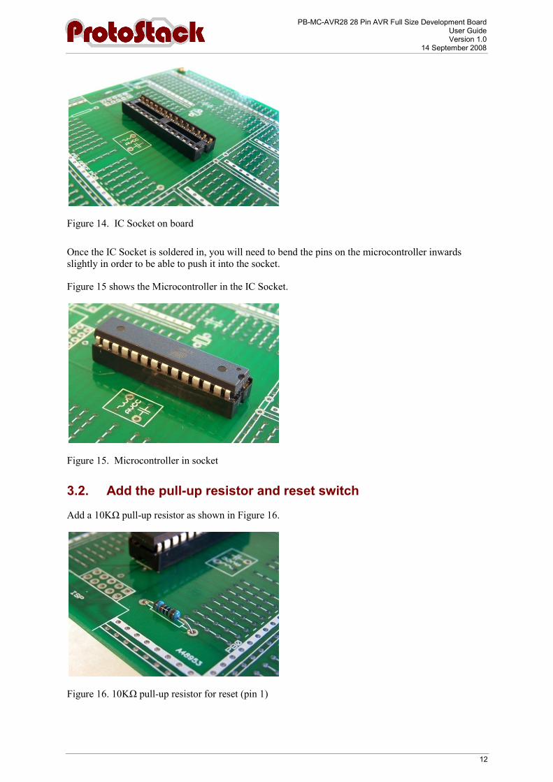
Although the microcontroller can be soldered directly onto the board, many people prefer to solder an IC socket onto the board then insert the microcontroller into the socket. This option does not expose the microcontroller to the high temperatures of soldering, and also allows for the removal and substitution of the microcontroller in the event that your project requires more flash memory or additional microcontroller features.
Figure 14 shows the IC socket on the board.
PB-MC-AVR28 28 Pin AVR Full Size Development Board User Guide Version 1.0
14 September 2008
12
Figure 14. IC Socket on board
Once the IC Socket is soldered in, you will need to bend the pins on the microcontroller inwards slightly in order to be able to push it into the socket.
Figure 15 shows the Microcontroller in the IC Socket.
Figure 15. Microcontroller in socket
3.2. Add the pull-up resistor and reset switch
Add a 10KΩ pull-up resistor as shown in Figure 16.
Figure 16. 10KΩ pull-up resistor for reset (pin 1)
PB-MC-AVR28 28 Pin AVR Full Size Development Board User Guide Version 1.0
14 September 2008
13
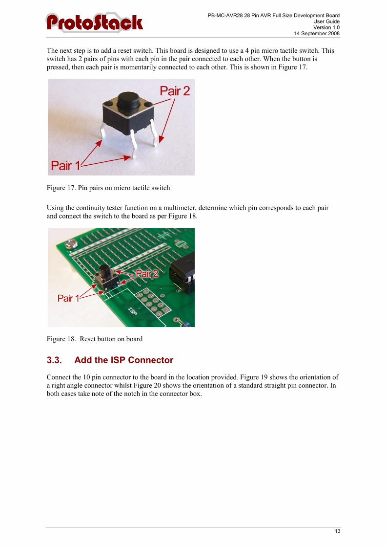
The next step is to add a reset switch. This board is designed to use a 4 pin micro tactile switch. This switch has 2 pairs of pins with each pin in the pair connected to each other. When the button is pressed, then each pair is momentarily connected to each other. This is shown in Figure 17.
Figure 17. Pin pairs on micro tactile switch
Using the continuity tester function on a multimeter, determine which pin corresponds to each pair and connect the switch to the board as per Figure 18.
Figure 18. Reset button on board
3.3. Add the ISP Connector
Connect the 10 pin connector to the board in the location provided. Figure 19 shows the orientation of a right angle connector whilst Figure 20 shows the orientation of a standard straight pin connector. In both cases take note of the notch in the connector box.

PB-MC-AVR28 28 Pin AVR Full Size Development Board User Guide Version 1.0
14 September 2008
14
Figure 19. ISP Right Angle Connector
Figure 20. ISP Straight Pin Connector
3.4. Wire up the AVCC Block
This board allows AVCC to be connected directly to VCC or connected via a low pass filter. Figure 21 shows AVCC connected to VCC With a jumper.
Figure 21. AVCC Connected to VCC with Jumper
To connect AVCC via a low pass filter, use a 10 µH inductor instead of the jumper and install a 100nF capacitor in the location shown.
PB-MC-AVR28 28 Pin AVR Full Size Development Board User Guide Version 1.0
14 September 2008
15
3.5. Add an external Oscillator
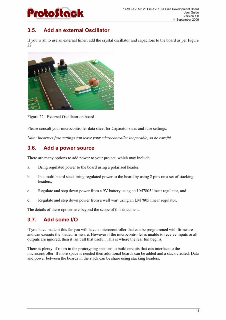
If you wish to use an external timer, add the crystal oscillator and capacitors to the board as per Figure 22.
Figure 22. External Oscillator on board
Please consult your microcontroller data sheet for Capacitor sizes and fuse settings.
Note: Incorrect fuse settings can leave your microcontroller inoperable, so be careful.
3.6. Add a power source
There are many options to add power to your project, which may include:
a. Bring regulated power to the board using a polarised header,
b. In a multi board stack bring regulated power to the board by using 2 pins on a set of stacking headers,
c. Regulate and step down power from a 9V battery using an LM7805 linear regulator, and
d. Regulate and step down power from a wall wart using an LM7805 linear regulator.
The details of these options are beyond the scope of this document.
3.7. Add some I/O
If you have made it this far you will have a microcontroller that can be programmed with firmware and can execute the loaded firmware. However if the microcontroller is unable to receive inputs or all outputs are ignored, then it isn’t all that useful. This is where the real fun begins.
There is plenty of room in the prototyping sections to build circuits that can interface to the microcontroller. If more space is needed then additional boards can be added and a stack created. Data and power between the boards in the stack can be share using stacking headers.
PB-MC-AVR28 28 Pin AVR Full Size Development Board User Guide Version 1.0
14 September 2008
16
4. Comment and Questions If you have any questions or comments regarding this documentation or any of our products, please post to the Protostack forum at http://www.protostack.com/forum/. The forum will allow you to interact with peers and are constantly monitored by our support engineers.


![Atmel AVR XMEGA A4 Datasheet - RS ComponentsTCD0:1 USARTD0:1 SPID EVENT ROUTING NETWORK PB[0..3] Int. Ref. AREFA AREFB Tempref VCC/10 7 8069R–AVR–06/2013 XMEGA A4 Not recommended](https://static.fdocuments.in/doc/165x107/60d6499aa3f607123a3cb22b/atmel-avr-xmega-a4-datasheet-rs-components-tcd01-usartd01-spid-event-routing.jpg)