Pavel Moreno-García1*, Andrea La Rosa2 š 1,3 2 , Koji ... with TOC_La Rosa-1.pdf · Pavel...
12
Pavel Moreno-García 1 *, Andrea La Rosa 2 * † , Viliam Kolivoška 1,3 *, Daniel Bermejo 2 , Wenjing Hong 1 , Koji Yoshida 1 , Masoud Baghernejad 1 , Salvatore Filippone 2 , Peter Broekmann 1 , Thomas Wandlowski 1 , Nazario Martín 2,4 * 1 Department of Chemistry and Biochemistry, University of Bern, Freiestrasse 3, CH-3012 Bern, Switzerland 2 Departamento de Química Orgánica, Facultad de Química, Universidad Complutense de Madrid, E-28040, Madrid, Spain 3 J.Heyrovský Institute of Physical Chemistry, AS CR, v.v.i., Dolejškova 3, 18223, Prague 8, Czech Republic 4 IMDEA-Nanoscience, Campus Universidad Autónoma, 28049-Madrid, Spain charge transport, single molecule conductance, fullerene, dumbbell-type molecules, scanning tunneling microscopy break junction, current sensing atomic force microscopy break junction, mechanically controlled break junction ABSTRACT: Single molecule charge transport characteristics of buckminsterfullerene-capped symmetric fluorene-based dumbbell-type compound (1) were investigated by scanning tunneling microscopy break junction (STM-BJ), current sensing atomic force microscopy break junction (CS-AFM-BJ) and mechanically controlled break junction (MCBJ) techniques, under ambient conditions. We also show that the compound 1 is able to form highly organized defect-free surface adlayers, allowing the molecules on the surface to be addressed specifically. Two distinct single molecule conductance states (called high G H 1 and low G L 1 ) were observed, depending on the pressure exerted by the probe on the junction, allowing thus molecule 1 to function as a mechanically driven molecular switch. These two distinct conductance states were attributed to the electron tunneling through the buckminsterfullerene anchoring group and fully extended molecule 1, respectively. The assignment of conductance features to these configurations was further confirmed by control experiments with asymmetrically designed buckminsterfullerene derivative ( 2) as well as pristine buckminsterfullerene (3), both lacking the G L feature. 1 Introduction Organic molecules employed as active device components within molecular electronic circuits could offer interesting technological opportunities to overcome the scaling limits of silicon-based technology. 1-4 To date, the ease to functionalize allotropes of carbon 5-8 has been exploited in applications in organic photovoltaics 9,10 and, in this context, devices have been prepared, which are capable of reaching energy conversion efficiencies up to 8 %. 11 Fullerenes constitute a particular class of molecules that have attracted the attention of the scientific community since their discovery in 1985. 12 They exhibit many unique properties and are particularly important as singular photo- and electro-active species in organic electronics. 13 In previous years, scanning probe spectroscopy experiments have been carried out on buckminsterfullerene C 60 adsorbed on noble metal surfaces to address its electronic characteristics. 14- 16 These investigations have shown that distinct specific adsorption orientations and geometries as well as intermolecular interactions strongly influence its electronic properties. 17-20 At the same time, advances in the manipulation of single molecules now permit one to contact them between two metal electrodes, 21-26 and study their electron transport characteristics to reveal the details of the formed molecular junctions. Thus, the capability of pristine fullerene C 60 to be trapped between two electrodes has been envisaged and achieved. 23,27-29 Thanks to its spherical geometry and the multi- interaction configurations of its carbon atoms with metal electrodes, it has been possible to measure the electric conductance across the molecule itself. Additionally, a variety of strategies for the synthesis of molecular wires with two fullerene-type anchoring sites (dumbbell-type molecules) has been developed. 30,31 Such molecules have been designed to act as molecular bridges between two electrodes in break junction studies. 32,33 This new class of molecules is promising due to an ease of functionalization, which allows incorporation of many linkers between the two C 60 termini. 30,31
Transcript of Pavel Moreno-García1*, Andrea La Rosa2 š 1,3 2 , Koji ... with TOC_La Rosa-1.pdf · Pavel...

Pavel Moreno-García1*, Andrea La Rosa
2*
†, Viliam Kolivoška
1,3*, Daniel Bermejo
2, Wenjing
Hong1, Koji Yoshida
1, Masoud Baghernejad
1, Salvatore Filippone
2, Peter Broekmann
1, Thomas
Wandlowski1, Nazario Martín
2,4*
1Department of Chemistry and Biochemistry, University of Bern, Freiestrasse 3, CH-3012 Bern, Switzerland 2Departamento de Química Orgánica, Facultad de Química, Universidad Complutense de Madrid, E-28040, Madrid,
Spain 3J.Heyrovský Institute of Physical Chemistry, AS CR, v.v.i., Dolejškova 3, 18223, Prague 8, Czech Republic 4IMDEA-Nanoscience, Campus Universidad Autónoma, 28049-Madrid, Spain
charge transport, single molecule conductance, fullerene, dumbbell-type molecules, scanning tunneling microscopy
break junction, current sensing atomic force microscopy break junction, mechanically controlled break junction
ABSTRACT: Single molecule charge transport characteristics of buckminsterfullerene-capped symmetric fluorene-based dumbbell-type compound (1) were investigated by scanning tunneling microscopy break junction (STM-BJ), current sensing atomic force microscopy break junction (CS-AFM-BJ) and mechanically controlled break junction (MCBJ) techniques, under ambient
conditions. We also show that the compound 1 is able to form highly organized defect-free surface adlayers, allowing the molecules on the surface to be addressed specifically. Two distinct single molecule conductance states (called high GH
1 and low GL
1) were
observed, depending on the pressure exerted by the probe on the junction, allowing thus molecule 1 to function as a mechanically driven molecular switch. These two distinct conductance states were attributed to the electron tunneling through the
buckminsterfullerene anchoring group and fully extended molecule 1, respectively. The assignment of conductance features to these configurations was further confirmed by control experiments with asymmetrically designed buckminsterfullerene derivative (2) as
well as pristine buckminsterfullerene (3), both lacking the GL feature.
1 Introduction
Organic molecules employed as active device components
within molecular electronic circuits could offer interesting technological opportunities to overcome the scaling limits of
silicon-based technology.1-4
To date, the ease to functionalize allotropes of carbon
5-8 has been exploited in applications in
organic photovoltaics9,10
and, in this context, devices have been prepared, which are capable of reaching energy
conversion efficiencies up to 8 %.11
Fullerenes constitute a particular class of molecules that have attracted the attention
of the scientific community since their discovery in 1985.12
They exhibit many unique properties and are particularly
important as singular photo- and electro-active species in organic electronics.
13
In previous years, scanning probe spectroscopy experiments
have been carried out on buckminsterfullerene C60 adsorbed on noble metal surfaces to address its electronic characteristics.
14-
16 These investigations have shown that distinct specific
adsorption orientations and geometries as well as intermolecular interactions strongly influence its electronic
properties.17-20
At the same time, advances in the manipulation of single molecules now permit one to contact them between
two metal electrodes,21-26
and study their electron transport characteristics to reveal the details of the formed molecular
junctions. Thus, the capability of pristine fullerene C60 to be trapped between two electrodes has been envisaged and
achieved.23,27-29
Thanks to its spherical geometry and the multi-interaction configurations of its carbon atoms with metal
electrodes, it has been possible to measure the electric conductance across the molecule itself. Additionally, a variety
of strategies for the synthesis of molecular wires with two fullerene-type anchoring sites (dumbbell-type molecules) has
been developed.30,31
Such molecules have been designed to act
as molecular bridges between two electrodes in break junction studies.
32,33 This new class of molecules is promising due to an
ease of functionalization, which allows incorporation of many linkers between the two C60 termini.
30,31

2
Location of a molecule adsorbed on a surface and
determination of its scanning probe spectroscopic properties while maintaining a tunneling gap has been achieved with
several molecules, such as naphthalocyanines34
and redox-active proteins.
35 However, the aim of the current study is to
wire a molecule by attaching both of its termini to metal electrodes. These experiments usually require low
temperatures and ultrahigh vacuum to suppress mobility of the adsorbed molecules along the substrate.
36 Nonetheless, recent
pioneering studies with dumbbell-type molecules under ambient conditions were reported.
32,33,37 Theoretical
calculations have demonstrated that the conductance of these molecules is dominated by the alignment of LUMO orbitals
with the electrode Fermi levels.38
Using a scanning tunneling microscopy (STM) setup, Leary et al.
33and Gillemot et al.
37
were able to image individual dumbbell molecules attached to gold substrates, and recorded subsequently the current through
isolated, single molecular nanojunctions by gently touching one of the bulky C60 anchoring groups with the STM tip. More
than one conductance state was found in these investigations. These experimental findings have been attributed to the
existence of distinct metal-molecule-metal geometrical configurations. In this context, our work aims at extending
these investigations by exploring electron transport of single molecular dumbbell junctions in a liquid phase with the
ultimate goal of potentially exploiting the electroactivity employing the concept of electrolyte gating (C60 is a unique
electron acceptor).39
Figure 1: Structures of molecules 1, 2 and 3.
In this paper, we report on the transport characteristics of a
fluorene-based dumbbell-type molecular wire (molecule 1 in Figure 1), in which two C60 moieties are covalently connected
to a central fluorene unit through the sp3
carbon atoms of a fused pyrrolidine ring
40. As this molecule is sufficiently large
to be imaged by STM, direct visualization of the molecule prior to the transport measurement allows carrying out single-
molecule electrical measurements under well-controlled conditions. Obtained single molecule charge transport
characteristics of 1 were compared to those of an asymmetrically designed buckminsterfullerene-capped
fluorene-based derivative as well as pristine C60 (molecules 2 and 3 in Figure 1). For the first time, we demonstrate STM tip
pressure controlled molecular conductance switching (between high and low molecular conductance states), realized under
ambient conditions (temperature and pressure) for an isolated molecule 1 at gold(111)/decane interface.
2 Experimental procedures
2.1 Synthesis and characterization of the compounds
The synthesis of dumbbell-type molecule 1 was carried out
by using the well-known Prato reaction on C60.41,42
Briefly, 2,7-diformyl-9,9-dihexylfluorene reacted with sarcosine (N-
methylglycine) in toluene at reflux temperature to form, via a
two-fold 1,3-dipolar cycloaddition reaction of the in situ generated azomethyne ylide with the double bond of C60,
molecule 1, which was obtained in 10% yield. In turn, 2,7-diformyl-9,9-dihexylfluorene was prepared from
commercially available 2,7-dibromofluorene by a dialkylation reaction in position 9, followed by a formylation reaction.
43,44
To corroborate the expected electronic structure and
investigate electron transfer (redox behavior) in molecules 1 to 3, their solutions were characterized by transmission UV-VIS
spectroscopy and cyclic voltammetry (see Figures S3 and S4 in the SI for details).
2.2 STM imaging experiments
Bead gold electrodes with 111 facets were used as substrates. They were cleaned by immersion in concentrated
sulfuric acid, ensuing electrochemical polishing and thorough rinsing with Milli-Q water (Millipore Corp.,
18.2 MΩ·cm, 2 ppb TOC). Prior to experiments, they were flame annealed by butane flame and cooled down to room
temperature under an argon stream (Carbagas, Alphagaz, 99.999%). The reconstruction of the surface was removed by
immersion of the as-prepared electrodes in 0.1 M HCl (diluted from 37%, for analysis, Merck) for 20 minutes. The electrodes
were then thoroughly rinsed with Milli-Q water to remove all chloride anions adsorbed on the electrode surface and dried in
a stream of argon. Mechanically cut Pt/Ir wires (80/20, Goodfellow, 0.25 mm in diameter) were employed as STM
probes. After assembling an STM Kel-F liquid cell to confine the liquid phase on top of the substrate, 90 μL of decane (99
%, Sigma-Aldrich) were added to prevent the adsorption of ambient impurities. The surface was then inspected by STM
imaging to verify their absence. Subsequently, 10 μL of 10 μM solution of 1 in toluene (99.8 %, Sigma-Aldrich) were added
to the liquid phase. In this way, submonolayers of 1 were found to be formed on the Au(111) surface via adsorption
from solution. Unlike 1, molecule 2 was found to be soluble in
decane and significantly more soluble in toluene. This allowed carrying out the STM experiments with concentrations of up
to 0.1 mM of 2 in decane. For the experiments performed with the molecule 3, we first immersed the electrode in its 17 μM
solution in toluene for 4 min. After rinsing with decane, such modified electrode was mounted to the liquid cell, and
subsequently 150 μL of decane were added to protect the surface. In all three cases, the entire STM setup was housed in
an all-glass argon-filled environmental chamber.
2.3 Charge transport measurements
Charge transport measurements were first performed using
the STM-based break junction (STM-BJ) technique.25,26
The adsorbate-modified substrates were prepared following the
protocol described in the Section 2.2. We used electrochemically etched gold wires (Goodfellow, 99.999%,
0.25 mm in diameter) as STM tips to form molecular junctions and investigated their transport characteristics through
symmetric Au‒molecule (1, 2 or 3)‒Au junctions. The approaching distance between the STM probe and the
electrode surface was controlled by a lab-made electronics and dedicated software. Complementary charge transport
experiments were carried out with 1 dissolved in mesitylene (98%, Sigma-Aldrich).
3
Additionally, charge transport experiments with molecule 1
were performed using the mechanically controlled break junction (MCBJ) technique. As this approach relies on the
formation of molecular junctions between two horizontally suspended electrodes,
45 we used a modified assembly
procedure, which is detailed as follows. First, control transport experiments were carried out in pure decane in the MCBJ
liquid cell. The obtained conductance-distance traces showed only quantized gold-gold contact features. Decane was then
evaporated by passing an argon flow and 0.1 mM solution of 1 in toluene (99.8%, Sigma-Aldrich) was then dropcast at 60 °C
onto the closed MCBJ nanojunction and allowed to be dried under argon flow. This step was repeated four times.
Subsequently the MCBJ nanojunction was opened and the dropcasting procedure was repeated three more times
employing the same solution of 1 at room temperature. When the solvent was completely evaporated, decane was injected
into the liquid cell on top of the central part of the MCBJ liquid cell, to avoid contamination from ambient atmosphere.
The system was deoxygenated by purging with an argon stream prior to the conductance measurements.
2.4 Force measurements
Electromechanical measurements were conducted using the conductive probe atomic force microscopy break junction
(CP-AFM) approach.46,47
Besides monitoring the electric current flowing through the nanojunctions, we simultaneously
recorded interaction forces within individual stretching cycles. The experimental setup was based on a modified Agilent
Picoplus 5500 system equipped with a 10 μm multi-mode AFM scanner with a contact-mode nose-cone. The electrically
conductive gold-coated Si AFM probes (PPP-NCSTAu, spring constant of 13 N m
-1) were purchased from NanoSensors.
They were cleaned by immersion in chloroform (98%, Acros Organics) and ethanol (94%, Dr Grogg Chemie AG, Basel)
followed by drying in argon flow (Carbagas, Alphagaz, 99.999%) and subsequent exposure to a UV-ozone cleaner
(Novascan) for 30 min. The parts of the AFM scanner
assembly, which were in contact with the solution during the experiments, were rinsed with isopropanol and afterwards
dried in argon flow. The AFM probe was mounted onto the AFM scanner with a metal clamp, which also provided the
electrical contact between the conductive gold film on the AFM probe and the lab-built current-to-voltage (i-V)
converter. Decane and the solution of 1 in toluene were injected to the liquid cell immediately after the mounting of
the setup was completed, as described in Section 2.2.
2.5 Electrochemical characterization
The cyclic voltammetric experiments were carried out either
with a home-made potentiostat48
or with commercially available Autolab platform (Metrohm, The Netherlands) in a
three-electrode electrochemical cell. All glassware was cleaned by an overnight immersion in caroic acid (see SI for
details), followed by repeated boiling and copious rinsing in Milli-Q water and subsequent drying in an oven. Solutions of
molecules 1 to 3 (0.125 mM) were prepared in a mixture of acetonitrile (99.99%, anhydrous, Fisher) and 1,2-
dichlorobenzene (99%, anhydrous, Sigma-Aldrich), in the ratio 1:4 v/v. TBAPF6 (99 %, Fluka for electrochemistry) was
added to all solutions as supporting electrolyte, at concentration of 0.1 M. The electrode potential scale as well
as the electron consumption of 1 to 3 was referenced to the
Fc/Fc+ couple (see Figure S4 in the SI for details).
3 Experimental results
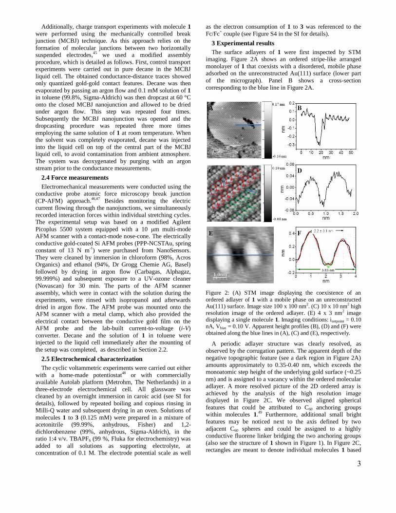
The surface adlayers of 1 were first inspected by STM imaging. Figure 2A shows an ordered stripe-like arranged
monolayer of 1 that coexists with a disordered, mobile phase adsorbed on the unreconstructed Au(111) surface (lower part
of the micrograph). Panel B shows a cross-section
corresponding to the blue line in Figure 2A.
Figure 2: (A) STM image displaying the coexistence of an
ordered adlayer of 1 with a mobile phase on an unreconstructed Au(111) surface. Image size 100 x 100 nm2. (C) 10 x 10 nm2 high resolution image of the ordered adlayer. (E) 4 x 3 nm2 image displaying a single molecule 1. Imaging conditions: isetpoint = 0.10 nA, Vbias = 0.10 V. Apparent height profiles (B), (D) and (F) were obtained along the blue lines in (A), (C) and (E), respectively.
A periodic adlayer structure was clearly resolved, as
observed by the corrugation pattern. The apparent depth of the negative topographic feature (see a dark region in Figure 2A)
amounts approximately to 0.35-0.40 nm, which exceeds the monoatomic step height of the underlying gold surface (~0.25
nm) and is assigned to a vacancy within the ordered molecular adlayer. A more resolved picture of the 2D ordered array is
achieved by the analysis of the high resolution image displayed in Figure 2C. We observed aligned spherical
features that could be attributed to C60 anchoring groups within molecules 1.
49 Furthermore, additional small bright
features may be noticed next to the axis defined by two
adjacent C60 spheres and could be assigned to a highly conductive fluorene linker bridging the two anchoring groups
(also see the structure of 1 shown in Figure 1). In Figure 2C, rectangles are meant to denote individual molecules 1 based
4
on two distinct models (red and green) of the surface adlayer.
The analysis of profiles pertaining to individual molecules based on these two models revealed a characteristic separation
distance between the centers of two adjacent spherical features amounting to (1.00 ± 0.20) nm (Figure 2D).
Since one of our main goals was to address charge transport
characteristics of a single dumbbell molecule 1, we also explored low-coverage adlayer regions. Interestingly, the latter
were found to coexist with ordered molecular adlayers and disordered phase, both shown in Figure 2A. In low coverage
areas, we identified well-isolated dumbbell molecules. After identifying their location, we monitored them over longer
distances and times to explore their strength of attachment to the Au(111) surface. Sufficiently strong binding to the gold
substrate is, in this context, essential for locating and lifting of an immobilized single molecule from the substrate to form a
molecular bridge between the substrate and the STM tip.33
Figure 2E shows a single dumbbell molecule 1 adsorbed in the
low coverage region. Similarly to what was observed in the monolayer of 1 (Figure 2C), a small bright feature may be
noticed next to the axis of the two bright C60 spheres, most probably related to the presence of the highly conductive
fluorene group bridging the two C60 anchoring groups (compare to Figure 1). The cross section associated with the
horizontal blue line in Figure 2E is displayed in Figure 2F. The center-to-center distance between the two C60 anchoring
sites is estimated as (2.20 ± 0.10) nm. However, it is larger than the theoretically estimated value (1.44 ± 0.04) nm.
50 This
mismatch may be caused by a thermal or tip induced movement of the molecule 1 on the gold surface. On the other
hand, the apparent height of the C60 anchoring group (0.40 nm,
Figure 2F) is in an excellent agreement with literature values (0.35 nm
and 0.40 nm
27 as well as with the vacancy depth in
the ordered molecular adlayer (0.35-0.40 nm, Figure 2A and B). The isolated dumbbell molecules could be imaged at very
low tunneling setpoint currents for roughly one hour provided the entire measurement system was stable enough. However,
at higher setpoint currents, we observed a higher surface mobility caused by displacement of the dumbbell molecule
with the STM probe (data not shown). Such mobility reflects limited attractive interactions between the gold surface and the
dumbbell molecule. This behavior is different from that in the ordered, closely-packed molecular adlayers. In the case of an
isolated molecule, there are no attractive intermolecular interactions, which would stabilize the molecule in its fixed
position. The observation of the high mobility differs from studies carried out in air with similar dumbbell systems by
Leary et al. 33
and Gillemot et al..37
Therefore, we conclude that the presence of a liquid phase (decane with 10 % of
toluene added due to solubility reasons) diminishes the strength of attractive interactions of the dumbbell molecules
with the gold surface.
Direct visualization of a single molecule prior to charge transport measurements through it is a significant step towards
improving the reliability of STM-BJ experiments. Further, working with rather diluted molecular adlayers reduces the
risk of their aggregation on the surface and therefore suppresses the interference from intermolecular interactions,
20
leading to preferential formation of metal-single molecule-
metal nanojuntions. Additional support for single molecule junctions in the STM-BJ setup is provided by recent
concentration-dependent charge transport experiments, which
lead to identical conductance, except that the junction formation probability decreases with decreasing
concentration.52
Upon STM imaging, we proceeded to investigate charge transport characteristics of formed nanojunctions at solid-
liquid interfaces. In a first stage, we performed control experiments on the unmodified gold electrodes covered by
decane (i.e. without molecules 1). We recorded hundreds of G-Δz traces employing the STM-BJ approach.
25,53 The individual
traces were processed further by constructing all-data-point 1D conductance histograms.
52 The latter constructed for gold-
gold junctions at gold/pure decane interface only displayed well known quantized conductance features at G ≥ G0 (data not
shown), with G0 = 77.5 μS, being the quantum of conductance. This result confirmed the cleanliness and proper operation of
the experimental setup. Next, we introduced the solution of 1 into the liquid cell following the strategy outlined in the
Section 2.2. We then carried out charge transport measurements by recording G-Δz characteristics at interfacial
regions, where the gold surface was covered by diluted monolayers of 1 (Figure 2E). The low surface coverage of 1
was found to lead to favorable conditions to form single molecule junctions during the continuous approach and
retraction probe cycles.
It is known that the transport characteristics through pristine C60 in STM-BJ measurements are strongly influenced by the
tensile stress and compressive deformation of C60 cage generated by the pressure exerted by the tip.
54 To account for
this source of conductance variation, we carried out
conductance-distance measurements by varying systematically the closest approaching distance of the tip relative to the
substrate surface. The latter was achieved by stopping the approach of the probe at a certain position with respect to the
surface, as defined by a preset value of the conductance, so-called trigger conductance Gtrigger, determined as Gtrigger =
itrigger/Vbias. The probe vertical movement was controlled via an external feedback loop. The value of Gtrigger applied in this
work spanned the range of -2.5 ≤ log(Gtrigger/G0) ≤ 1.5, where G0 refers to the conductance quantum. The movement of the
probe was either stopped so that a physical contact between the probe and the substrate was prevented (log(Gtrigger/G0) < 0),
or established (log(Gtrigger/G0) ≥ 0) (see below).
Figure 3A shows a typical sample G-Δz curve acquired with log(Gtrigger/G0) = -1.0. The black trace represents the
approaching G-Δz curve part. The retracting part is plotted as green trace. The majority of the G-Δz curves exhibit well-
defined plateaus around log(G/G0) ~ -3.0 to -4.0 and around log(G/G0) ~ -5.0 to -6.0 that interrupt a characteristic steep
decay before and after their appearance, which is assigned to direct electron tunneling through the solvent in the junction
both during the approaching and retraction of the STM tip.
Figures 3B and 3C show further typical withdrawal traces and the corresponding 1D conductance histogram constructed
from 558 individual retracting curves, respectively. The histogram displays two well-separated conductance features at
high, log(GH1/G0) ~ -3.2, and low, log(GL
1/G0) ~ -5.9 region,
with both features having a relatively narrow distribution. This
observation differs from the results of Ref. 33, in which the
STM-BJ method in air was used and no clearly spaced features

5
were observed using the same representation. We assign the
two molecular features to the most probable conductance states, GH
1 and GL
1, through a single molecule 1 trapped
between metal leads for the particular trigger value log(Gtrigger/G0) = -1.0 (justifying thus an increased data density
around this value, see Figure 3C). The existence of the two molecular features GH
1 and GL
1 is also supported by the two-
dimensional representation of the conductance as a function of the tip displacement.
53 Figure 3D shows the 2D conductance
histogram, which was constructed with the same data as in panel 3C. The G-Δz curves were aligned at log(G/G0) = -6.0 as
common point (this value is just above the detection limit of the measurement electronics detected when the tip is far from
the surface, denoted by asterisks in Figure 3). Panels 3A and 3B (green curves) demonstrate that the high conductance state
always precedes the low conductance feature as the tip is being retracted from the adlayer covered substrate (low
surface coverage!). On the other hand, the high conductance state follows the occurrence of the low conductance feature for
the approaching curves (Figure 3A, black).
Figure 3: Typical approaching (A, black) and retracting (A, B,
green) G-∆z curves recorded with log(Gtrigger/G0) = -1.0. (C) and (E) show 1D conductance histogram constructed from 558 and 186 withdrawing curves at log(Gtrigger/G0) = -1.0 and 1.5, respectively. (D) and (F) show 2D histograms corresponding to the data in (C) and (E). The traces were aligned at log(G/G0) = -6.0 (D) and -0.2 (F). Vbias = 0.03 V, tip rate v = 58 nm s-1.
We then decreased systematically the distance of the closest
approach between the tip and the gold substrate, by increasing
the trigger level value. For each Gtrigger value, we recorded and analyzed the conductance data independently. Figure 3E
shows the 1D conductance histogram obtained from 186 withdrawing curves by applying log(Gtrigger/G0) = 1.5, i.e. with
the physical contact between gold leads created. The sharp
peak at log(G/G0) = 0 represents the conductance of a monatomic gold constriction just before the contact between
the two Au electrodes breaks upon further retraction of the tip. The 2D representation of these data displayed in Figure 3F is
obtained by aligning all conductance traces at a relative origin of log(G/G0) = -0.2.
53 This choice is justified by a sharp decay
in conductance value upon rupture of the last gold-gold contact in the course of the STM probe retraction.
Figure 4 summarizes the dependence of the molecular
conductance on the Gtrigger value. The existence of both high and low conductance states (GH
1, GL
1) is preserved upon
varying the Gtrigger value. We found that GH1 increases by up to
two orders of magnitude as the Gtrigger value increases (blue
circles). However, GL1 value remains practically unchanged
(log(GL1/G0) ~ -5.5, red circles).
Figure 4: Dependence of the GH1 (blue) and GL
1 (red) values of 1
as a function of Gtrigger. Full and empty circles represent average values obtained from approaching and withdrawing curves, respectively. Gray crosses represent STM-BJ data with 1 dissolved in mesitylene. Black and green empty circles correspond to complementary MCBJ and CP-AFM-BJ data, respectively.
Previous work by Schull et al.55
in ultrahigh vacuum
demonstrated that the conductance of C60 rises as the STM tip progressively presses it, because the latter leads to an increase
in contact area and an effective decrease of distance between
gold leads. We note that the conductance is in all cases larger for the approaching traces (full circles) than for the retracting
counterparts (empty circles). We also investigated charge transport properties of 1 dissolved in mesitylene bulk (0.2
mM) to verify whether the molecule 1 could be trapped directly from the solution to form a molecular bridge between
the electrodes. Applying log(Gtrigger/G0) = 1.0, we obtained the two most probable conductance values log(GH
1/G0) = -2.8 and
log(GL1/G0) = -5.0, from 2604 withdrawing curves (grey
crosses in Figure 4). For details, see Figure S5 in the SI.
Complementary conductance measurements using the
MCBJ method were carried out to verify the STM-BJ results. Since this technique forms molecular junctions between two
horizontally suspended gold electrodes, we employed a different molecular deposition strategy (Section 2.3). We
recorded 10700 G-Δz retracting traces applying log(Gtrigger/G0) = 1.0. The conductance distributions obtained upon plotting all
retracting traces without any data selection did not show any clear conductance features. Closer inspection of the raw data
revealed that no molecular plateaus were observed in most of the cycles. Upon disregarding curves showing only pure

6
tunneling events, i.e. those exhibiting exponential decay upon
the tip retraction, we found that only 30 % and 7 % of the cycles showed the GH
1 and the GL
1 states, respectively (see
Figure S6 in the SI for details). The low junction formation probability is understandable because when employing the
MCBJ technique combined with the abovementioned molecular deposition strategy, one cannot inspect a new
surface area as in the STM-BJ technique when the adsorbed molecule is depleted from the studied substrate location. The
availability of the molecules bridging the junction is therefore lower and the probability to successfully form molecular
junctions is accordingly expected to be decreased. The conductance values extracted from Gaussian fits of the peak-
shaped features after the abovementioned data selection procedure are represented in Figure 4 by black symbols
(log(GH1/G0) = -2.2 and log(GL
1/G0) = -5.0) (see Figure S6 in
the SI for details). They are slightly above the trends found by
the STM-BJ technique (see dashed lines).
Figure 5: (A) A characteristic withdrawing G-∆z curve recorded by CP-AFM-BJ. (B) 2D conductance histogram (black) and corresponding master curve (red). (C) F-∆z curve recorded simultaneously with G-∆z curve in (A). (D) 2D force histogram obtained for FL
1 feature (black) and corresponding master curve (red). Obtained with log(Gtrigger/G0) = 1.0 Vbias = 0.030 V, v = 50 nm s-1.
As another complementary experimental technique, we used conductive-probe atomic force microscopy break junction
(CP-AFM-BJ) method.46,47
The latter provides an access to simultaneous dynamic assessment of the force coupled to the
electric current detection during the evolution of the nanojunction.
46,47 This allows finding correlations between
molecular conductance and force as the molecular junction breaks. The experimental assembly conditions were the same
as for the STM-BJ based charge transport experiment (see Section 2.2). We recorded 3769 G-Δz retracting curves
applying log(Gtrigger/G0) = 1.0, while simultaneously monitoring the interaction force between the substrate and the
AFM probe. One characteristic retracting conductance-distance trace is shown in Figure 5A. Similarly to STM-BJ, we
resolved two most probable conductance features GH1 and GL
1
(highlighted in the 2D conductance histogram shown in Figure
5B by blue ellipses). Additionally, we constructed a master
curve (Figure 5B, red profile) by averaging all log(G/G0)
values (a Gaussian fit used) at all given displacement values Δz. The average molecular conductance values (log(GH
1/G0) =
-2.8 ± 0.6 and log(GL1/G0) = -5.1 ± 0.5) obtained by CP-AFM-
BJ technique were extracted from the corresponding 1D
histogram (see Figure S7 in the SI for details) and are denoted by empty green symbols in Figure 4. The conductance values
fit well to the trends found by the STM-BJ technique (dashed lines).
Figure 5C displays the force-distance curve acquired
simultaneously with the conductance-distance curve shown in Figure 5A. Three force “jumps” at 0.02, 0.20 and 0.30 nm
were observed, i.e. simultaneously with an abrupt decrease of the junction conductance (compare Figure 5C to Figure 5A).
The first force jump reflects a plastic deformation of the junction, in the course of which the last Au-Au bond of the
junction breaks (the junction conductance drops by three orders of magnitude), leaving a molecule 1 bridging the
electrodes. The jump at 0.20 nm, denoted as FH1
in Figure 5C, reflects a junction transition from the high to the low
molecular conductance state, as documented by a concomitant decrease of the junction conductance value from GH
1 to GL
1.
The latter observed force jump (at 0.30 nm, denoted as FL1)
originates from the breaking of the molecular junction, as
evidenced by an abrupt drop of the conductance value to the detection limit of the measurement electronics (log(G/G0) ≈ -
6.0). Similarly, the value of the interaction force gradually reaches 0 nN (Figure, 5C), indicating the departure of the
probe from the electrode surface. We constructed a 2D representation of all force-distance traces that showed a clear
force jump (FL1)
at ∆z values corresponding to the end of the
low conductance feature (GL1) by aligning them according to
the distance scale shift obtained by the alignment of
corresponding conductance-distance traces to zaligned = 0 nm at G = 0.1 GL
1. The resulting force histogram is shown in
Figure 5D. The red line superimposed on top of this 2D force histogram displays the force-distance master curve obtained
by averaging all force values at each value of the aligned
displacement zaligned. The vertical distance of the two force
profiles (blue dashed lines in Figure 5D, obtained by linear
fitting of the master curve for zaligned < 0 and zaligned > 0,
respectively) extrapolated to zaligned = 0, allows estimating the most probable breaking force of the junction in the GL
1
state. This force amounts to ca. 0.4 nN. In a similar way we estimated the rupture force of molecular junctions containing 1
in the GH1 state, amounting to ca. 0.7 nN (see Figure S8 in the
SI for details). Interestingly, the latter force value is very close
to the one reported for a (dative covalent) Au-N bond at a gold/molecule interface (FAu-N = (0.8 ± 0.2) nN
46). On the
other hand, force values obtained in the present work are much smaller than the most probable breaking force value found for
the rupture of the Au-Au bond (1.5 nN).47,56,57
This indirectly indicates that, most probably, an Au-C bond is broken in the
junction containing a molecule 1.
For the data obtained by the STM-BJ technique, we also carried out a careful analysis of the characteristic molecular
plateau length (denoted as ∆zH1
for GH1 and ∆z
L1 for GL
1
features, see Figure 6A-B for characteristic profiles), as a
function of the trigger level (Figure 6C-D). The conductance boundaries for the plateau length determination were 0.1 GH
1 ≤

7
G ≤ 10 GH1 and 0.1 GL
1 ≤ G ≤ 10 GL
1 for GH
1 and GL
1,
respectively. Comparison of Figures 6A and 6B shows that the approaching curves exhibit considerably longer plateau
lengths for both conductance states than the withdrawing curves. Additionally, the characteristic plateau length of the
GL1 state, Δz
L1, shows a more noticeable dependence on the
Gtrigger than GH1 (Figure 6C-D): Δz
L1 increases with Gtrigger (red
data points) while the data for ΔzH1
scatters and does not show a clear trend (blue data points). Finally, Δz
L1 for the
approaching curves reaches a plateau value around 2.0 nm as log(Gtrigger/G0) values are above -1.0 (Figure 6C, red data
points). Interestingly, this value is in good agreement with the length of molecule 1 (2.1 ± 0.1 nm)
50 (see below).
Figure 6: Distributions of ∆zH1 (blue) and ∆zL
1 (red) obtained from approaching (A) and withdrawing (B) curves using log(Gtrigger/G0) = -1.2. (C) and (D) dependence of the ave-rage plateau length values of approaching (C) and withdrawing (D) events as a function of Gtrigger. Vbias = 0.03 V, v = 58 nm s-1.
The conductance through pristine C60 confined between two
noble metal leads has been studied in vacuum.15,27,29
and under ambient conditions.
58 More than one conductance state was
observed for pristine C60 in ultrahigh vacuum experiments. The difference was attributed to the sensitivity of C60 to the contact
geometry on noble metal electrodes. Berndt et al.15,55,59,60
showed that different adsorption configurations of C60 on
metal substrates modify the tunneling current across the molecule when it is contacted by an STM tip. With the
exception of Ref. 27 all observed values are in the range log(G/G0) = -1.0 to 0.2.
29,37,54,55,58-65 The difference in
conductance (up to factor of 20)55
of these distinct states is,
however, much lower than that one of the two well-discernible GH
1 and GL
1 features that we resolved for 1 (compare blue and
red trend lines in Figure 4). We suggest therefore that different contact geometries of the C60 anchoring groups cannot account
for the existence of these two distinctly observed conductance states of molecule 1. Additionally, the spread of the most
probable conductance values GH1 and GL
1 is comparable to
their absolute difference (Figure 3C-F). Molecule 1 possesses
a conjugated fluorene system in its central part that leads to efficient delocalization of electric charge between the two C60
anchoring groups (Figure 1). However, each C60 group is attached to the central fluorene moiety via two electron
saturated linkers. This may, in principle, decrease in a
noticeable way the transport efficiency of the whole molecule 1. The degree of conjugation between the three components
(two C60 anchoring groups and the linker between them) of related dumbbell-type molecules is crucial for electronic
transmission across the molecular bridge.40
Moreover, the transport through differently-capped biphenyls (fluorene
including) has been comprehensibly studied 66,67
and could be described by a non-resonant tunneling mechanism. This means
that the conductance across the molecular bridge decreases exponentially with its length and is independent of
temperature. Therefore, one could then expect that the conductance through an extended molecule 1 connected to two
metal leads should be remarkably lower than the conductance of a pristine C60 due to both the interruption of conjugation by
the saturated (sp3-type) carbon atoms (Figure 1) and the
significantly larger length of the fully extended molecule 1.
Based on the above arguments, we are lead to propose that the two distinct molecular conductance states of 1 (GH
1 and GL
1)
are originated from two different configurations of the whole molecule of 1 in the junction. They are illustrated in the Figure
7. Within this scenario, the GL1 state is assigned to the
configuration of molecule 1 bridging the junction with each
C60 anchor attached to one of the two metal electrodes, i.e. tip and substrate. The GH
1 state is attributed to a single C60
anchoring group being trapped between the two leads.
Figure 7: Evolution (approaching/retracting cycles) of the STM-
BJ experiment with molecule 1.
The whole stretching cycle may be visualized as follows: In a first stage of the junction evolution, the STM tip is being
approached towards the surface modified by molecule 1
(Figure 7A). When the gap separation is close to the molecular
length, one C60 anchoring group of the molecule jumps into contact with the tip due the thermal motion or applied electric
field (Figure 7B). The low conductance state of the junction GL
1 is reached and the electric current flows through the entire
molecule 1, including the fluorene linker. Alternatively, by the action of the force exerted by the probe on the molecular
junction, the molecule 1 may change conformation (not shown in Figure 7B). Due to a short length of the fluorene linker, the
two C60 moieties may get close to each other, causing their π-systems to overlap, creating thus an additional conductance
channel. However, at this stage, we cannot conclusively say if the electron transport in the GL
1 state of the molecular junction
is secured solely by the fluorene linker or is assisted by this

8
additional C60-C60 conductance channel. The C60 anchoring
group attached to the tip is then confined and eventually compressed between tip and substrate (Figure 7C).
Alternatively, the sliding of the C60 anchoring group along the tip may be possible and the conductance would have
contributions from the molecular channel as well as from direct tunneling through the solvent. Upon tip retraction, the
decompression or reintroduction of the C60 group into the nanogap takes place (Figure 7D). The fully extended
molecular junction is formed again via attachment of the molecule between tip and substrate through both C60 anchoring
groups (Figure 7E). Possibly, an alternative conductance channel leading through two mutually connected C60
anchoring groups may be operative (not shown in Figure 7E). Finally, the molecular junction breaks (Figure 7F). This
interpretation is supported by the occurrence sequence of the GH
1 and GL
1 features (compare Figure 7B to E to Figure 3A)
and the evolution of the characteristic plateau length in the two molecular conductance states. As mentioned above, Figure 6
illustrates that the approaching curves exhibit considerably higher plateau lengths for the low conductance feature than the
withdrawing curves. The characteristic length of the low conductance state Δz
L1, particularly for the approaching curves
is rather close to the length of a molecule 1 being completely extended (~2.2 nm). This is reasonable as the molecule jumps
into contact with the tip as soon as the latter is close enough to form an Au-1-Au junction, with completely extended
molecule 1. However, the average withdrawing plateau length (Figure 6D) is shorter because during the retraction, the
molecule may detach from the tip before complete elongation
is reached, due to the weak coupling of C60 on Au in decane, caused by the thermal motion of the molecule 1 within the
junction. On the other hand, the ΔzH1
values are shorter than the length of a fully extended molecule 1 (Figure 6C-D, blue
symbols) and this suggests the trapping of one C60 anchoring group, which can be compressed or elongated over much
shorter distances than the whole molecule 1. The characteristic length of the high conductance feature Δz
H1, however, is
sometimes also larger than the actual size of the C60 moiety. This might suggest that the fluorene moiety could attach to the
tip which would further stabilize the molecular junctions in the GL
1 state as it was found in Ref. 37.
As illustrated in Figure 4, GH1 value increases by up to two
orders of magnitude as the Gtrigger value increases (blue data points). By increasing the Gtrigger value, the effective gap
distance between the two electrodes decreases, causing that the tip exerts a certain pressure on the molecule located within
the junction, explaining thus the above trend. The low conductance value GL
1 is, however, rather insensitive to the
Gtrigger value (red data points in Figure 4). This reflects a certain conformational flexibility of the fully extended
molecule 1 in the junction. We remind that the existence of the two conductance states, GH
1 and GL
1, was also corroborated by
MCBJ and CP-AFM-BJ measurements (see Figures 4 and 5 as well as Figures S6 to S8 in the SI).
In an attempt to further rationalize the physical meaning of
the two conductance states of 1, we used STM-BJ technique to further explore transport characteristics of two additional
molecules. The molecule 2 (the asymmetric counterpart of 1,
see Figure 1) bears only one C60 anchoring group attached to the fluorene moiety. The second reference molecule to be
inspected further was pristine fullerene C60 (3, see Figure 1).
The conductance measurements of 2 were carried out with a rather large bulk concentration in comparison to 1 (0.1 mM for
2 vs. 1 M for 1), since it was not possible to immobilize molecules 2 on the unreconstructed Au(111) substrate due to
their higher solubility in decane.
We explored the molecular conductance and plateau length dependence of 2 and 3 on the Gtrigger value in the same fashion
as for the molecule 1. The individual G-Δz curves as well as 1D and 2D conductance histograms (Figure 8A-B, data shown
for log(Gtrigger/G0) = 0.40) obtained for 2 displayed only one molecular feature. The dependence of the latter on the Gtrigger
value (Figure 8C) follows qualitatively well the corresponding dependence constructed for GH
1 feature (Figure 4, blue
circles), and is therefore further referred to as GH2.
Figure 8: (A) 1D and (B) 2D conductance histograms of 2
constructed from 186 withdrawing curves with log(Gtrigger/G0) = 0.40. (C) Conductance and (D) plateau length dependence on Gtrigger. Vbias = 0.03 V, v = 58 nm s-1. Filled and empty circles denote the data of approaching and withdrawing events, respectively.
The corresponding average values of plateau length
distributions as a function of the trigger level (Figure 8D) also show that the length over which the junction in the GH
2 state
coincides relatively well to that of GH1, obtained for the
approaching events (Figure 6C). The withdrawing events
(Figure 8D, empty circles) obtained for 2 exhibit, however, slightly longer plateaus than in the case of 1 (Figure 6D, blue
circles). Additionally, we notice that the highest conductance GH
2 that we found (log(GH
2/G0) = -1.01, Figure 8C) matches
the value of Ref. 37 when only one C60 moiety of a related dumbbell compound was trapped between gold electrodes.
The value obtained in this work is also rather close to the results found in the literature for pristine C60 immobilized
between gold nanoelectrodes in air (log(G/G0) = -1.00)58
and vacuum (log(G/G0) = -1.00 and log(G/G0) = -0.70)
29,61 but
significantly higher than other reference27
(log(G/G0) = -3.60). Our value is, on the other hand, lower than the conductance of
C60 trapped between copper (log(G/G0) = -0.87 to 0.18)
,54,55,59,60,62-64
platinum (log(G/G0) = -0.15) ,65
and silver (log(G/G0) = -0.30)
61electrodes.
9
We also carried out transport experiments with molecule 3
and found a unique GH3 feature in both the 1D and 2D
histograms, as exemplified in Figure 9A-B (the data shown
here were obtained with log(Gtrigger/G0) = 0.40). The GH3
dependence on the trigger level (Figure 9C) follows a similar
trend as that found for GH1 (Figure 4, blue symbols) and GH
2
(Figure 8C). The maximum conductance found by us for 3
(log(GH3/G0) = -2.20, Figure 9C) is considerably higher than
that reported by Joachim et al. (log(G/G0) = -3.6),27
but lower
than data communicated by the authors of Refs. 29,58 and 61 (range of -1.0 ≤ log(G/G0) ≤ -0.7). The plateau length
dependence on Gtrigger of 3 is displayed in Figure 9D and indicates that the GH
3 state remains stable for slightly longer
distances as the Gtrigger value is increased.
Transport experiments with molecules 2 and 3 revealed only one conductance feature (Figures 8A and 9A), which exhibited
a similar dependence of GH2 and GH
3 on Gtrigger (Figures 8C
and 9C) as GH1
(Figure 4, blue circles). The conductance
values of all three molecules increase as the trigger level rises. The latter is related to a decreased electrode separation,
increasing the transport efficiency and nanogap contact area.
Figure 9: (A) 1D and (B) 2D conductance histograms for 3 constructed from 558 withdrawing curves with log(Gtrigger/G0) = 0.40. (C) Conductance and (D) plateau length dependence on Gtrigger. Vbias = 0.03 V, v = 58 nm s-1. Filled and empty circles denote the data of the approaching and withdrawing events, respectively.
The absolute values of single molecule conductance are however not the same. For example, taking as reference the
conductance obtained at log(Gtrigger/G0) = 0.20, the difference between GH
2 and GH
3 amounts to ca. half an order of
magnitude (expressed in the logarithmic scale, compare Figures 8C and 9C). Furthermore, the maximum high
conductance values of molecules 1 and 3 (both log(GH/G0) ≈ -2.2, Figure 4 and 9C), are one order of magnitude lower than
reported values for C60 29,37,54,58-65
, but much larger than the value reported by Joachim, et al..
27 The conductance of
molecule 2 obtained at log(Gtrigger/G0) > 1.25 (log(GH2/G0) ≈ -
1.1, Figure 8C) is in a good agreement with the former reports.
The difference in conductance observed for GH* (* stands
for 1, 2 or 3), following the trend GH2 > GH
1 > GH
3, originating
from trapping of a C60 anchoring group between gold leads,
cannot be accounted for by an experimental error. Consideration of the Δz
H* values may shade light into the
origin of these differences. As mention above, the characteristic length distribution follows the trend Δz
H2 > Δz
H1
> ΔzH3
. This suggests that possible attachment of the fluorene bridge in molecules 1 and 2 to the tip may contribute to the
longer distances that these molecular structures can be elongated upon existence of the GH* feature as compared to
molecule 3 (having no fluorene group). Within this scenario, the extra interaction of the fluorene bridge with the gold tip
would also involve additional overlapping of the metallic orbitals and the fluorene π-system (see Figure 7). This, in turn,
would explain why GH1 and GH
2 are larger than GH
3 (pristine
fullerene does not possess the additional molecular
conductance channel).
However, this scenario does not explain why the GH2 is
larger than GH1. Our argument to account for this difference is
as follows. The presence of an additional free C60 anchoring group in 1 (absent in molecule 2) before formation of the
completely elongated molecular junction decreases the stability of the through-fluorene attachment due to steric
reasons or thermal movement. In this way, the physical and electronic coupling between fluorene linker in 1 and tip would
be less strong leading to lower transport efficiency (in other words, molecular conductance value) and a correspondingly
shorter characteristic plateau length value.
A final comment is related to the possibility of locally addressing energetic states of the molecules 1 to 3 under
study. All of them are redox-active, having multiple redox
states. Under our experimental electrochemical conditions, neutral and two reduced states of molecules 1 to 3 could be
accessible (see Figure S4 in the SI for details). Their electroactivity may represent a platform for constructing
multi-state redox molecular switches, being addressable under electrochemical conditions (i.e. by the electrolyte gating
concept). The latter is currently intensively investigated in our laboratory. We also emphasize that the immobilization of the
molecules into ordered defect-free adlayers might in the future allow „writing“ and „reading“ the (electro)chemical state of
the molecules, by the aid of a scanning probe, allowing thus the adlayers to serve as molecular memories.
5 Conclusions
In summary, we have studied charge transport properties of
the fluorene-containing dumbbell-type molecular wire 1 under ambient conditions (temperature and pressure) employing the
molecular self-assembly deposition strategy in a liquid environment. We were able to image ordered molecular
assemblies as well as isolated molecules on the unreconstructed Au(111) substrate. Transport experiments in
an STM-BJ configuration revealed two conductance states, GH
1 and GL
1 that may be intentionally switched by the pressure
exerted by the STM probe. Based on transport studies of related systems performed in ultrahigh vacuum
59,60, this large
difference cannot be accounted for by mere variations in the contact geometry between the C60 anchoring groups and the
gold leads. The analysis of the evolution of the two states upon approaching and retraction of the STM tip suggests that the
GL1 feature corresponds to molecular junctions with 1 attached
via each C60 anchoring site to two distinct leads at opposite

10
sides of the extended molecule. In other words, the molecule is
extended along its axis in the junction. In this state of the molecular junction, the presence of an additional conductance
channel may be proposed, running through the two C60 anchoring groups, being put together by the pressure exerted
by the probe. The GH1 feature appears when the distance
between the two gold electrodes is significantly shorter. We
ascribe this junction configuration to a single C60 anchoring group trapped between the two adjacent electrodes. This
assignment is also supported by the absence of the GL1 states
in complementary transport experiments with molecule 2,
which bears only one C60 anchoring site and with pristine buckminsterfullerene 3. The GH
1 conductance state is strongly
dependent on the pressure exerted on the C60 group by the tip, with the junction conductance increasing by up to two orders
of magnitude. The molecular conductance value is the lowest when the C60 is touched gently and reaches the maximum
when it is strongly compressed or displaced along the edge of the tip. This represents a unique mechanical switching
capability of molecule 1. The agreement in the values of the junction conductance of 1, 2 and 3 is rather qualitative. GH
2 is
one order of magnitude larger than the corresponding values for GH
1 and GH
3.
CP-AFM experiments also allowed exploring the breaking
forces of molecular junctions formed by molecule 1 as trapped between two gold leads. We obtained average rupture forces
amounting to 0.4 and 0.7 nN for the low and the high molecular conductance state, respectively. The latter value
compares well to that obtained in molecular junctions, in which an Au-N bond is broken (0.8 nN). On the other hand,
the average values found in this work are markedly lower than
that known for the rupture of an Au-Au bond (1.5 nN). This indirectly proves that an Au-C bond is broken in the junction.
Finally, we remind that the unique electrochemical
properties of C60 and its derivatives provide opportunities to construct multi-state redox switching at the single molecule as
well as the molecular ensemble level.
Supporting Information. Synthesis and characterization of the compounds 1 to 3, Additional data of charge transport measurements obtained by MCBJ, CP-AFM-BJ and STM-BJ, Optimized geometry of 1. This material is available free of charge via the Internet at http://pubs.acs.org.
* Pavel Moreno-García, E-mail: [email protected] * Andrea La Rosa, E-mail: [email protected]
* Viliam Kolivoška, E-mail: [email protected] * Nazario Martín, E-mail: [email protected]
† Department of Chemical and Pharmaceutical Sciences, University of Trieste, Piazzale Europa 1, 34127 Trieste, Italy
The authors declare no competing financial interest.
This work was generously supported by the Swiss National Science Foundation (200021-124643; NFP 62), the German Science Foundation (priority program SPP 1243), the UK EPSRC, the EC FP7 ITN “FUNMOLS” project no. 212942, European Commission (Community Research and Development
Information Service, MOLESCO, project reference 606728) and the University of Bern. P. M.-G. also acknowledges support from CONACyT, Mexico (209297). V. K. acknowledges the financial support from SCIEX (Project Code 10.209) and Grant Agency of the Czech Republic (project No. 14-05180S). Financial support by the Ministerio de Ecoomía y Competitividad (MINECO) of Spain (project CTQ2011-24652). N.M. thanks to the Alexander von Humboldt Foundation.
STM-BJ, scanning tunneling break junction; CS-AFM-BJ, current sensing atomic force microscopy break junction; MCBJ, mechanically controllable break junction.
(1) Molecular Electronics: An Introduction to Theory and Experiment; Cuevas, J. C., Scheer, E, Ed.; World
Scientific: Singapore, 2010.
(2) Aviram, A.; Ratner, M. A. Chem. Phys. Lett. 1974, 29, 277-283.
(3) Flood, A. H.; Stoddart, J. F.; Steuerman, D. W.; Heath, J. R. Science 2004, 306, 2055-2056.
(4) Hush, N. S. An overview of the first half-century of molecular electronics. In Molecular Electronics III;
Reimers, J. R., Picconatto, C. A., Ellenbogen, J. C., Shashidhar, R., Eds.; New York Acad Sciences: New York,
2003; Vol. 1006; pp 01-20. (5) Guldi, D. M., Martin, N. Fullerenes: From Synthesis
to Optoelectronic Properties; Academic Publishers: Dordrecht, 2003; Vol. 4.
(6) Hirsch, A., Brettreich, M. Fullerenes, Chemistry and Reactions; Wiley-VCH: Weinheim, 2005.
(7) Langa, F. N., Nierengarten, J.-F. Fullerenes: Principles and Applications; RSC: Cambridge, 2007.
(8) Martin, N. Chem. Commun. 2006, 2093-2104. (9) Thompson, B. C.; Frechet, J. M. J. Angew. Chem. Int.
Edit. 2008, 47, 58-77. (10) Luis Delgado, J.; Bouit, P.-A.; Filippone, S.; Angeles
Herranz, M.; Martin, N. Chem. Commun. 2010, 46, 4853-4865.
(11) Huo, L.; Zhang, S.; Guo, X.; Xu, F.; Li, Y.; Hou, J. Angew. Chem. Int. Edit. 2011, 50, 9697-9702.
(12) Kroto, H. W.; Heath, J. R.; Obrien, S. C.; Curl, R. F.; Smalley, R. E. Nature 1985, 318, 162-163.
(13) Guldi, D. M.; Illescas, B. M.; Ma Atienza, C.; Wielopolskia, M.; Martin, N. Chem. Soc. Rev. 2009, 38,
1587-1597. (14) Lu, X. H.; Grobis, M.; Khoo, K. H.; Louie, S. G.;
Crommie, M. F. Phy. Rev. B. 2004, 70, 115418.
(15) Schull, G.; Neel, N.; Becker, M.; Kroeger, J.; Berndt, R. New J. Phys. 2008, 10, 065012.
(16) Sanchez, L.; Otero, R.; Maria Gallego, J.; Miranda, R.; Martin, N. Chem. Rev. 2009, 109, 2081-2091.
(17) Grobis, M.; Lu, X.; Crommie, M. F. Phy. Rev. B. 2002, 66, 161408.
11
(18) Rogero, C.; Pascual, J. I.; Gomez-Herrero, J.; Baro,
A. M. J. Chem. Phys. 2002, 116, 832-836. (19) Silien, C.; Pradhan, N. A.; Ho, W.; Thiry, P. A. Phys.
Rev. B. 2004, 69, 115434. (20) Torrente, I. F.; Franke, K. J.; Pascual, J. I. J. Phys.:
Condens. Matter 2008, 20, 184001. (21) Reed, M. A.; Zhou, C.; Muller, C. J.; Burgin, T. P.;
Tour, J. M. Science 1997, 278, 252-254. (22) Reichert, J.; Ochs, R.; Beckmann, D.; Weber, H. B.;
Mayor, M.; Lohneysen, H. V. Phys. Rev. Lett. 2002, 88, 176804-176804.
(23) Park, H.; Park, J.; Lim, A. K. L.; Anderson, E. H.; Alivisatos, A. P.; McEuen, P. L. Nature 2000, 407, 57-60.
(24) Cui, X. D.; Primak, A.; Zarate, X.; Tomfohr, J.; Sankey, O. F.; Moore, A. L.; Moore, T. A.; Gust, D.; Harris,
G.; Lindsay, S. M. Science 2001, 294, 571-574. (25) Xu, B. Q.; Tao, N. J. J. Science 2003, 301, 1221-
1223. (26) Li, C.; Pobelov, I.; Wandlowski, T.; Bagrets, A.;
Arnold, A.; Evers, F. J. Am. Chem. Soc. 2008, 130, 318-326.
(27) Joachim, C.; Gimzewski, J. K.; Schlittler, R. R.; Chavy, C. Phys. Rev. Lett. 1995, 74, 2102-2105.
(28) Parks, J. J.; Champagne, A. R.; Hutchison, G. R.; Flores-Torres, S.; Abruna, H. D.; Ralph, D. C. Phys. Rev.
Lett. 2007, 99, 026601. (29) Boehler, T.; Edtbauer, A.; Scheer, E. Phys. Rev. B.
2007, 76, 125432. (30) Segura, J. L.; Martin, N. Chem. Soc. Rev. 2000, 29,
13-25.
(31) Leary, E.; La Rosa, A.; González, M. T.; Rubio-Bollinger, G.; Agraït, N.; Martín, N. Chem. Soc. Rev. 2014
DOI: 10.1039/C4CS00264D. (32) Martin, C. A.; Ding, D.; Sorensen, J. K.; Bjornholm,
T.; van Ruitenbeek, J. M.; van der Zant, H. S. J. J. Am. Chem. Soc. 2008, 130, 13198-13199.
(33) Leary, E.; Gonzalez, M. T.; van der Pol, C.; Bryce, M. R.; Filippone, S.; Martin, N.; Rubio-Bollinger, G.;
Agrait, N. Nano Lett. 2011, 11, 2236-2241. (34) Liljeroth, P.; Repp, J.; Meyer, G. Science 2007, 317,
1203-1206. (35) Della Pia, E. A.; Chi, Q.; Jones, D. D.; Macdonald, J.
E.; Ulstrup, J.; Elliott, M. Nano Lett. 2011, 11, 176-182. (36) Zandvliet, H. J. W. Chimia 2012, 66, 52-55.
(37) Gillemot, K.; Evangeli, C.; Leary, E.; La Rosa, A.; Teresa Gonzalez, M.; Filippone, S.; Grace, I.; Rubio-
Bollinger, G.; Ferrer, J.; Martin, N.; Lambert, C. J.; Agrait, N. Small 2013, 9, 3812-3822.
(38) Markussen, T.; Settnes, M.; Thygesen, K. S. J. Chem. Phys. 2011, 135, 144104.
(39) Morita, T.; Lindsay, S. J. Phys. Chem. B 2008, 112, 10563-10572.
(40) Sorensen, J. K.; Fock, J.; Pedersen, A. H.; Petersen, A. B.; Jennum, K.; Bechgaard, K.; Kilsa, K.; Geskin, V.;
Cornil, J.; Bjornholm, T.; Nielsen, M. B. J. Org. Chem. 2011, 76, 245-263.
(41) Maggini, M.; Scorrano, G.; Prato, M. J. Am. Chem. Soc. 1993, 115, 9798-9799.
(42) Prato, M.; Maggini, M. Acc. Chem. Res. 1998, 31,
519-526.
(43) Hughes, G.; Wang, C. S.; Batsanov, A. S.; Fern, M.;
Frank, S.; Bryce, M. R.; Perepichka, I. F.; Monkman, A. P.; Lyons, B. P. Org. Biomol. Chem. 2003, 1, 3069-3077.
(44) Giuseppone, N.; Lehn, J. M. J. Am. Chem. Soc. 2004, 126, 11448-11449.
(45) Hong, W.; Valkenier, H.; Meszaros, G.; Manrique, D. Z.; Mishchenko, A.; Putz, A.; Garcia, P. M.; Lambert, C. J.;
Hummelen, J. C.; Wandlowski, T. Beilstein J. Nanotechnol. 2011, 2, 699-713.
(46) Xu, B. Q.; Xiao, X. Y.; Tao, N. J. J. Am. Chem. Soc. 2003, 125, 16164-16165.
(47) Pobelov, I. V.; Meszaros, G.; Yoshida, K.; Mishchenko, A.; Gulcur, M.; Bryce, M. R.; Wandlowski, T.
J. Phys.: Condens. Matter 2012, 24, 164210. (48) Meszaros, G.; Li, C.; Pobelov, I.; Wandlowski, T.
Nanotechnology 2007, 18, 424004. (49) Chavy, C.; Joachim, C.; Altibelli, A. Chem. Phys.
Lett. 1993, 214, 569-575. (50) CS Chem3D Ultra Molecular Modeling and Analysis;
7.0.0. ed.; CambridgeSoft, 2001. (51) Katsonis, N.; Marchenko, A.; Fichou, D. Synth. Met.
2003, 137, 1453-1455. (52) Moreno-García, P.; Gulcur, M.; Manrique, D. Z.;
Pope, T.; Hong, W.; Kaliginedi, V.; Huang, C.; Batsanov, A. S.; Bryce, M. R.; Lambert, C.; Wandlowski, T. J. Am.
Chem. Soc. 2013, 135, 12228-12240. (53) Hong, W.; Manrique, D. Z.; Moreno-García, P.;
Gulcur, M.; Mishchenko, A.; Lambert, C. J.; Bryce, M. R.; Wandlowski, T. J. Am. Chem. Soc. 2012, 134, 2292-2304.
(54) Hauptmann, N.; Mohn, F.; Gross, L.; Meyer, G.;
Frederiksen, T.; Berndt, R., New J. Phys. 2012, 14, 073032. (55) Schull, G.; Frederiksen, T.; Arnau, A.; Sanchez-
Portal, D.; Berndt, R. Nat. Nanotechnol. 2011, 6, 23-27. (56) Rubio-Bollinger, G.; Bahn, S. R.; Agrait, N.;
Jacobsen, K. W.; Vieira, S. Phys. Rev. Lett. 2001, 87, 026101.
(57) Frei, M.; Aradhya, S. V.; Koentopp, M.; Hybertsen,
M. S.; Venkataraman, L. Nano Lett. 2011, 11, 1518-1523. (58) Evangeli, C.; Gillemot, K.; Leary, E.; Teresa
Gonzalez, M.; Rubio-Bollinger, G.; Lambert, C. J.; Agrait, N. Nano Lett. 2013, 13, 2141-2145.
(59) Neel, N.; Kroeger, J.; Limot, L.; Frederiksen, T.; Brandbyge, M.; Berndt, R. Phys. Rev. Lett. 2007, 98,
065502. (60) Neel, N.; Kroeger, J.; Limot, L.; Berndt, R. Nano
Lett. 2008, 8, 1291-1295. (61) Zhao, J.; Murakoshi, K.; Yin, X.; Kiguchi, M.; Guo,
Y.; Wang, N.; Liang, S.; Liu, H. J. Phys. Chem. C 2008, 112, 20088-20094.
(62) Schulze, G.; Franke, K. J.; Gagliardi, A.; Romano, G.; Lin, C. S.; Rosa, A. L.; Niehaus, T. A.; Frauenheim, T.;
Di Carlo, A.; Pecchia, A.; Pascual, J. I. Phys. Rev. Lett. 2008, 100, 136801.
(63) Schull, G.; Frederiksen, T.; Brandbyge, M.; Berndt, R. Phys. Rev. Lett. 2009, 103, 206803.
(64) Strozecka, A.; Muthukumar, K.; Dybek, A.; Dennis, T. J.; Larsson, J. A.; Myslivecek, J.; Voigtlaender, B. Appl.
Phys. Lett. 2009, 95, 133118. (65) Kiguchi, M. Appl. Phys. Lett. 2009, 95, 073301.

12
(66) Venkataraman, L.; Klare, J. E.; Nuckolls, C.;
Hybertsen, M. S.; Steigerwald, M. L. Nature 2006, 442, 904-907.
(67) Mishchenko, A.; Zotti, L. A.; Vonlanthen, D.; Buerkle, M.; Pauly, F.; Carlos Cuevas, J.; Mayor, M.;
Wandlowski, T. J. Am. Chem. Soc. 2011, 133, 184-187.