Partial Discharge Pattern of Various Defects Measured … · Partial Discharge Pattern of Various...
17
International Journal on Electrical Engineering and Informatics ‐ Volume 6, Number 2, June 2014 Partial Discharge Pattern of Various Defects Measured by Spiral Antenna as UHF External Sensor on 66 kV GIS Model Umar Khayam 1 , Widya Anggoro Putro 2 , Sriyono 2 , Koji Urano 3 , Chen Min 3 , Suwarno 1 , Masahiro Kozako 4 , and Masayuki Hikita 4 1 School of Electrical Engineering and Informatics, Institut Teknologi Bandung, Indonesia 2 PT PLN (Persero), Indonesia 3 SE Technology, Hongkong 4 Department of Electrical Engineering, Kyushu Institute of Technology, Japan [email protected] Abstract: This paper deals with partial discharge (PD) measurement in gas insulated switchgear (GIS) using spiral antenna as UHF external sensor. PD detection in UHF band is effective because it detects electromagnetic (EM) wave induced by PD with high S/N ratio. External sensor was used to detect leaked EM wave signals from insulation spacer of GIS tank. The experiment was conducted in 66 kV GIS model with metal type spacer. There is insulation window in the spacer. PD was generated by some artificial defects in GIS and an external PD source. The leaked EM wave propagated through spacer aperture was measured using spiral type sensor without filter and amplifier. The peak to peak value (Vpp) and the transmission rate of electromagnetic wave signals were evaluated. The PD patterns were observed. The results showed that the PD was detected by the spiral antenna. PD pattern was unique for each defect. These results are considered to be useful for enhancement of database PD diagnosis. Keywords – partial discharge, external sensor, spiral antenna, UHF detection, PD pattern 1. Introduction Detection of partial discharge (PD) is useful for condition monitoring of gas insulated switchgear (GIS) [1-8]. For the insulation diagnosis of GIS, the ultra-high frequency (UHF) method which detects PD induced electromagnetic wave (EM-wave) in the UHF band (300 MHz to several GHz) with little noise influence, has rapidly developed in recent years [9-18]. It is necessary to install a sensor inside or set on the outside of a GIS tank to detect partial discharge (PD) signals that propagate inside a GIS. For GISs that have already been constructed, it is effective to use external diagnosis using EM-wave signals that radiate (leak) from the insulation spacer of the GIS tank [19]. For a metal spacer, there is usually an insulation aperture in the spacer which enables EM-wave to radiate. Some external sensors for PD detection in GIS have been examined recently such as bowtie antenna, horn antenna, and loop antenna [20-30]. In this research the spiral antenna was examined to measure PD in 66 kV GIS model. PD was generated by some artificial PD sources; those are protrusion on the high voltage conductor, protrusion on the tank, floating electrode, free particle, void, particle on the spacer, and aerial/external defects. PD pattern was measured by spiral antenna as UHF sensors and observed by PD monitoring device. These results are considered to be useful for enhancement of database PD diagnosis. 2. Experimental Setup A. GIS Model The experimental setup was arranged as shown in Figure 1. The 66 kV GIS model was used in the experiment. GIS 66 kV structure is composed of coaxial cylindrical electrodes with high voltage conductors and insulating spacers. The GIS central conductor is 80 mm in diameter and GIS tank was 200 mm in diameter. Each gas section is 1000 mm in length, except for the end Received: February 24 th , 2013. Accepted: June 23 rd , 2014 404 404
Transcript of Partial Discharge Pattern of Various Defects Measured … · Partial Discharge Pattern of Various...

International Journal on Electrical Engineering and Informatics ‐ Volume 6, Number 2, June 2014 Partial Discharge Pattern of Various Defects Measured by Spiral Antenna
as UHF External Sensor on 66 kV GIS Model
Umar Khayam1, Widya Anggoro Putro2, Sriyono2, Koji Urano3, Chen Min3, Suwarno1, Masahiro Kozako4, and Masayuki Hikita4
1School of Electrical Engineering and Informatics, Institut Teknologi Bandung, Indonesia 2PT PLN (Persero), Indonesia 3SE Technology, Hongkong
4Department of Electrical Engineering, Kyushu Institute of Technology, Japan [email protected]
Abstract: This paper deals with partial discharge (PD) measurement in gas insulated switchgear (GIS) using spiral antenna as UHF external sensor. PD detection in UHF band is effective because it detects electromagnetic (EM) wave induced by PD with high S/N ratio. External sensor was used to detect leaked EM wave signals from insulation spacer of GIS tank. The experiment was conducted in 66 kV GIS model with metal type spacer. There is insulation window in the spacer. PD was generated by some artificial defects in GIS and an external PD source. The leaked EM wave propagated through spacer aperture was measured using spiral type sensor without filter and amplifier. The peak to peak value (Vpp) and the transmission rate of electromagnetic wave signals were evaluated. The PD patterns were observed. The results showed that the PD was detected by the spiral antenna. PD pattern was unique for each defect. These results are considered to be useful for enhancement of database PD diagnosis. Keywords – partial discharge, external sensor, spiral antenna, UHF detection, PD pattern
1. Introduction Detection of partial discharge (PD) is useful for condition monitoring of gas insulated switchgear (GIS) [1-8]. For the insulation diagnosis of GIS, the ultra-high frequency (UHF) method which detects PD induced electromagnetic wave (EM-wave) in the UHF band (300 MHz to several GHz) with little noise influence, has rapidly developed in recent years [9-18]. It is necessary to install a sensor inside or set on the outside of a GIS tank to detect partial discharge (PD) signals that propagate inside a GIS. For GISs that have already been constructed, it is effective to use external diagnosis using EM-wave signals that radiate (leak) from the insulation spacer of the GIS tank [19]. For a metal spacer, there is usually an insulation aperture in the spacer which enables EM-wave to radiate. Some external sensors for PD detection in GIS have been examined recently such as bowtie antenna, horn antenna, and loop antenna [20-30]. In this research the spiral antenna was examined to measure PD in 66 kV GIS model. PD was generated by some artificial PD sources; those are protrusion on the high voltage conductor, protrusion on the tank, floating electrode, free particle, void, particle on the spacer, and aerial/external defects. PD pattern was measured by spiral antenna as UHF sensors and observed by PD monitoring device. These results are considered to be useful for enhancement of database PD diagnosis. 2. Experimental Setup A. GIS Model The experimental setup was arranged as shown in Figure 1. The 66 kV GIS model was used in the experiment. GIS 66 kV structure is composed of coaxial cylindrical electrodes with high voltage conductors and insulating spacers. The GIS central conductor is 80 mm in diameter and GIS tank was 200 mm in diameter. Each gas section is 1000 mm in length, except for the end
Received: February 24th, 2013. Accepted: June 23rd, 2014
404404

conductor with connected gas compartment with total length is 1500 mm. The insulating spacer is made from epoxy resin with a cone-shaped structure (relative dielectric constant = 4). The outer periphery of the insulating spacer is clad with aluminium and part of the epoxy resin is exposed bare. The exposed part of the epoxy resin (spacer aperture) is 65 mm in length and 15 mm width. The gas compartment was filled with SF6 gas at 0.15 MPa.
Figure 1. Experimental setup and condition
B. PD charge calibration Before the main experiment, the charge calibration was conducted using a pulse calibrator as shown in Figure 2. The charge was injected from a pulse calibrator into GIS bushing and the output was measured by an oscilloscope. The charge calibration results are shown in Figure 3. The PD apparent charge can be estimated when the voltage measured using CD6 based on the conventional method (IEC 60270) is known.
Figure 2. Charge calibration of experimental setup
Umar Khayam, et al.
405

Figure 3. Charge calibration I (Volt & mv) C. Spiral Antenna as UHF PD Sensor The leaked EM wave propagated through spacer aperture was measured using spiral type sensor. For PD pattern measurement, three spiral antennas as UHF sensors (named as A, B, C) placed on the aperture spacer. The sensors were connected to the channel switch as a power supply. The output of the channel switch was connected to PDM device and the oscilloscope and the computer. The envelope processing and amplification were processed in PDM device. The PD pattern was observed and recorded in the computer. For transmission rate evaluation, two spiral sensors without envelope processing & amplifier (called as original sensor) connected to spacer A and spacer B. The sensors were connected to an oscilloscope (oscilloscope Tektronix, DPO4104, 1 GHz, 5 GS/s). The PD detecting device (CD-6) based on conventional method IEC 60270 was used as comparison. We used limit resistance 200 kΩ, coupling capacitor 2 nF, and RC detection impedance (R constant = 50 ohm and C variable = 470 pF). The voltage was converted into apparent charge based on the calibration result using the charge calibrator. Partial discharge was measured using partial discharge monitoring (PDM) device, oscilloscope voltage / current-time graph, and conventional method IEC 60270. D. Artificial PD Source Figure 4 shows seven artificial defects used in this experiment. Those are: protrusion on the high voltage conductor (POC), protrusion on the tank (POT), floating electrode (FLOATING), free metal particle (FMP), particle on the spacer (POS), void / delamination (DEL) and aerial defect (OUTSIDE). Protrusion on the high voltage conductor (HVC) is a 5 cm needle electrode (Ogura) attached on the conductor. The curvature of the needle tip was 30˚. The gap between the needle tip and the tank was 1 cm. PDIV from above configuration was 6 kV. Protrusion on the tank was made similar with protrusion on the high voltage conductor. PDIV from protrusion on the tank was 11 kV. Floating electrode defect made from steel with 20 mm in length was floating in SF6 gas by being tied to a piece of string attached to the side walls of the tank. The gap length between the conductor and the tip of maximum position of floating electrode was 5 mm. PDIV for this model was 23 kV. Two free metal particle defects made from steel with length 1 cm was attached to both end of a 12 cm string adhered in middle to the side wall. PDIV for this model was 15 kV. Particle on the spacer is made from steel adhered to the top side of the spacer. The length of steel was 1 cm with the gap between the conductor and the spacer was 1 cm. We placed a piece of spacer on the bottom side of tank with 5 cm in height. PDIV for this model was 45 kV.
Partial Discharge Pattern of Various Defects Measured by Spiral Antenna
406

Void / delamination defect is made from resin with 0,3 mm air gap. The length of void was 3 mm. We placed the resin connected to the conductor on the topside and grounded to the tank on the bottom side. Aerial outside defect made from needle-plane electrode with gap 1 mm was directly connected to GIS. PDIV from this model was 3 kV.
Protrusion on the high voltage conductor (HVC)
Protrusion on the Tank (TANK)
Floating electrode (FLOATING)
Free Metal Particle (FMP)
Particle on Spacer (POS)
Umar Khayam, et al.
407

Defects on GIS outside (AERIAL)
Delamination (DEL)
Figure 4. Seven different artificial PD defects 3. Experimental Results Partial discharges are represented by several parameters: PD inception voltage (Vi) in [kV], phase angle of PD occurrence and PD number or PD frequency in a specific time or phase angle. Figures 5-11 show PD emitted EM waveform from the various defects.
Figure 5. PD induced EM waveform from protrusion on high voltage conductor measured by
external sensors in 66 kV GIS model
Partial Discharge Pattern of Various Defects Measured by Spiral Antenna
408
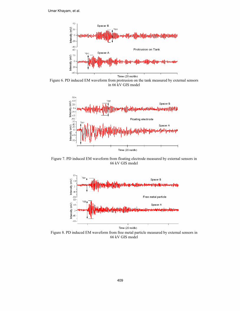
Figure 6. PD induced EM waveform from protrusion on the tank measured by external sensors
in 66 kV GIS model
Figure 7. PD induced EM waveform from floating electrode measured by external sensors in 66 kV GIS model
Figure 8. PD induced EM waveform from free metal particle measured by external sensors in
66 kV GIS model
Umar Khayam, et al.
409

Figure 9. PD induced EM waveform from particle on the spacer measured by external sensors in 66 kV GIS model
Figure 10. PD induced EM waveform from aerial defect (PD source outside GIS) measured by external sensors in 66 kV GIS model
Figure 11 PD induced EM waveform from delamination model measured by external sensors
in 66 kV GIS model
Partial Discharge Pattern of Various Defects Measured by Spiral Antenna
410

Figures 12-18 show PRPD pattern measured by external spiral type antenna sensor.
PDIV = 6 kV SP A SP B SP C
12 kV
SP A SP B SP C
Figure 12. PD Pattern of protrusion on HVC measured by external sensors with spiral antenna
in 66 kV GIS
PDIV = 12.5 kV SP A SP B SP C
17.5 kV
SP A SP B SP C
Figure 13. PD Pattern of protrusion on the tank measured by external sensors with spiral
antenna in 66 kV GIS
PDIV = 23 kV SP A SP B SP C
27 kV
SP A SP B SP C
Figure 14. PD Pattern of floating electrode measured by external sensors with spiral antenna in
66 kV GIS
Umar Khayam, et al.
411

PDIV = 15 kV SP A SP B SP C
21.5 kV
SP A SP B SP C
Figure 15. PD Pattern of Free metal particle measured by external sensors with spiral antenna
in 66 kV GIS
PDIV = 48 kV SP A SP B SP C
54 kV SP A SP B SP C
Figure 16. PD Pattern of Particle on spacer measured by external sensors with spiral antenna in
66 kV GIS
PDIV = 3 kV SP A SP B SP C
4 kV
SP A SP B SP C
Figure 17. PD Pattern of Aerial Defects measured by external sensors with spiral antenna in 66 kV GIS
Partial Discharge Pattern of Various Defects Measured by Spiral Antenna
412

PDIV = 8 kV
12 kV
Delamination model
Figure 18. PD Pattern of Delamination model measured by external sensors with spiral antenna
in 66 kV GIS 4. ANALYSIS & DISCUSSION A. Phase Resolved PD Pattern The experiment results are analyzed and discussed based on statistical approach, trending, and graph or table. First we examined PRPD pattern data. PRPD patterns presented here were recorded in uni-polar mode with time of acquisition of 120 seconds. Characteristics of PD for pattern recognition and classification are computed from the relation of the voltage phase angle, the discharge magnitude and the repeated existing of PD using statistical analysis. The PD quantity as function of the phase angle represent the recurrence of PD related to their phase angle [31-33]. The voltage cycle is divided into phase window representing the angle axis (0–360°). The four quantities can be determined in each phase window as follows: 1. The sum of the discharge magnitudes observed in one phase window (discharge amount). 2. The number of discharges observed in one phase window (pulse count). 3. The average value of discharges observed in one phase (mean pulse height). 4. The maximum value of discharge observed in one phase window (maximum pulse height). Table 1 summarizes the specific PD occurrence phase angle of each artificial defect. Protrusion on high voltage conductor (POC) defect shows that discharges pulses occurred in negative half cycles. The discharges were concentrated around the peak of the negative half cycle of the applied voltage which indicated that the discharges occurrence was mainly influenced by the instantaneous applied voltage. This phenomenon was due to the availability of initial electrons which were easily ejected from needle tip to initiate negative discharges.
Table 1 Specific PD occurrence phase angle of each artificial defect
Umar Khayam, et al.
413

Protrusion on tank (POT) defect shows that discharges pulses occurred in positive half cycles. It is also influenced by instantaneous applied voltage because positive ions on HV conductor side affect the appearance of negative ion (electron) on the ground side (tank). Then, initial electrons are ejected from needle tip to initiate discharges. Floating electrode (FLOATING) defect shows that discharges pulses occurred in 225˚ and 45˚. It indicates that discharges occurred under voltage rise and fall (time derivative of applied voltage dv/dt is positive on the left side and negative on the right side). This indicates that discharge occurrence depends on the slope/gradien of the applied voltage. Free metal particle (FMP) defect shows that discharges pulses occurred as a random in voltage phase. It indicates that the discharges occurrence influenced by the instantaneous applied voltage. As a free particle, they can behave like a protrusion on the conductor/tank or floating metal. Therefore they have combination pattern from protrusion and floating metal. Particle on spacer (POS) defect shows that discharges pulses occurred in 45˚ and 225˚. It can be explained that the spacer acts as capacitor in which there are charging and discharging process. Besides that, influence of particle existences give a reason that discharge still depend on instantaneous applied voltage. Therefore they undergo like phase shift because of space charge process and also act as particle. B. Statistical Characteristic of PD Pattern Table 2 summarizes statistical characteristics of PD for various defects. H n( ) represents the number of the observed discharges in each phase window as a function of the phase angle. Hqn ( ) is mean pulse height distribution which represents the average amplitude in each phase window as a function of phase angle. Hq n max ( ) represents maximum amplitude in each phase window as a function of phase angle.
Table 2. Statistical Characteristic of PRPD pattern for various defects
Table 3 summarizes skewness and kurtosis of PD pattern characteristics for various defects. Skewness is a measure of symmetry, or more precisely, the lack of symmetry. A distribution, or data set, is symmetric if it looks the same to the left and right of the center point. Kurtosis is a measure of whether the data are peaked or flat relative to a normal distribution. That is, data sets with high kurtosis tend to have a distinct peak near the mean, decline rather rapidly, and have heavy tails. Data sets with low kurtosis tend to have a flat top near the mean rather than a sharp peak.
Discharges / Problem
Hq n max ( ) +
Hq n max ( ) ‐
Hq n ( )+ Hq n ( )‐ Hn ( ) + Hn ( ) ‐
Protrusion on HVC (POC)
‐ 240.6 ‐ 117.5 ‐ 185.4
Protrusion on Tank (POT)
110 22.5 21.8 1.1 154.7 4.2
Floating electrode (FLOATING)
8.9 11.9 2.1 3.8 5.1 6.7
Free metal particle (FMP)
11.9 32.1 3.8 4.1 17.4 21.3
Particle on spacer (POS)
18.2 20.1 2.2 2.3 13.1 14.2
Void / delamination (DEL)
14.1 14.6 2.9 3.1 19.5 20.4
Aerial / GIS outside (OUTSIDE)
18.6 4.8 3.5 1.8 20.5 4.7
Partial Discharge Pattern of Various Defects Measured by Spiral Antenna
414

Table 3. Kurtosis & Skewness values from various defects
It can be concluded that there is tendency kurtosis give positive result for protrusion on the tank defect, aerial defect, and particle on the spacer defect and negative result for the rest. On the other side, there is tendency that skewness of all defects almost give symmetric pattern, so skewness value tend to zero value. It can be explained because of the effect of symmetrical role of the electrode system (i.e needle-ground electrode) in producing discharges. Figure 19 shows apparent charge from different defects measured based on IEC 60270. It was seen that floating electrode (FL) defect gives the largest apparent charge and followed by aerial defects charge. Floating electrode is not connected into conductor or tank (ground), so they will result in big discharge once exceed the threshold. Free metal particle and particle on spacer defects give small apparent charge. Free metal particle (FMP) defect result small apparent charge due to mobile effect, meanwhile particle on spacer (POS) defect result small apparent charge due to combination between spacer existence and small protrusion. From above explanation, the apparent charge results does not seem to be correlated with UHF measurement.
Figure 19. Apparent charge of various defects measured by partial discharge detection in 66 kV
GIS Figure 20 shows Transmission Rate based on Vpp comparison. The transmission rate (TRAB) is defined as a comparison between intensity of PD induced electromagnetic wave measured by sensor B (length from PD source = 1,5 m) compare to one measured by sensor A (length from PD source = 0,5 m). The transmission rate (TR) informs attenuation (damping) characteristics because of the spacer presence and the propagation properties. It was obvious from Figure 20 that the average transmission rate is about 70% except floating electrode and aerial defect.
Protrusion on HVC (POC)
Protrusion on Tank (POT)
Floating electrode (FLOATING)
Free metal particle (FMP)
Particle on spacer (POS)
Void / delamination
(DEL)
Aerial / GIS outside
(OUTSIDE)
ku+ ‐ 1.1 ‐0.5 ‐1.1 2 ‐1.2 1.4
ku‐ ‐1.1 ‐ ‐0.5 ‐0.5 2 ‐1.1 ‐
sk+ ‐ 0.1 0 ‐0.1 ‐0.2 0.1 0.3
sk‐ 0.1 ‐ 0 0 0 0.5 ‐
Umar Khayam, et al.
415

Figure 20. Transmission Rate based on Vpp comparison between 2 sensors on spacer A and
spacer B 5. Conclusion We investigated PD pattern from several artificial defects measured with spiral antenna type as the external UHF sensors in 66 kV GIS model. The results showed that PD PRPD Pattern and PD waveform of each defect their own characteristic that differ from each other. Specific PD phase angle and statistical analysis of each artificial defect result various characteristic. Floating electrode defect gives the largest apparent charge the transmission rate of each artificial defect was about 70%. These results are considered to be useful for the enhancement of PD database PD measured by the external sensor. 6. References [1] M. D. Judd, O. Farish, and B.F. Hampton, “The Excitation of UHF Signals by Partial
Discharges in GIS”, IEEE Trans. Dielectr. Electr. Insul., Vol. 3, pp.213-228, 1996. [2] T. Hoshino, H. Koyama, S. Maruyama, and M. Hanai, "Comparison of Sensitivity
between UHF Method and IEC 60270 for On-site Calibration in Various GIS," IEEE Trans. Power Delivery, Vol. 21, No. 4, pp. 1948-1953, 2006.
[3] S.M.Hoek, U.Riechert, T.Streh, S.Tenbohlen and K. Feser, “A New Procedure for Partial Discharge Localization in Gas-Insulated Switchgears in Frequency Domain”,14thInt’l. Sympos. High Voltage Eng. (ISH), Paper No.G-05,2005.
[4] S.M. Hoek, M. Koch and M. Heindl,“Propagation Mechanisms of PD Pulses for UHF and Traditional Electrical Measurements”, Int’l. Conf. Condition Monitoring and Diagnosis, Paper No. C2-2, 2010.
[5] M. Hanai, F. Endo, S. Okabe, T. Kato, H. Hama, and M. Nagao, “New development for detecting partial discharge using an UHF method and its application to power apparatus in Japan,” CIGRE,2006.
[6] S. Okabe, S. Kaneko, M. Yoshimura, H. Muto, C. Nishida and M. Kamei, “Partial Discharge Diagnosis Method Using Electromagnetic Wave Mode Transformation in Gas Insulated Switchgear”, IEEE Trans. Dielectr. Electr. Insul., Vol. 14, No. 3, pp. 702-709, 2007.
[7] M. Yoshimura, H. Muto, C. Nishida, M. Kamei, S. Okabe and S. Kaneko, “Propagation Properties of Electromagnetic Wave through T-branch in GIS”, IEEE Trans. Dielectr. Electr. Insul., Vol. 14, No. 2, pp.328-333, 2007.
[8] A. J. Reid, and M. D. Judd, “High Bandwidth Measurement of Partial Discharge Pulses in SF6,” 14thInt’l. Sympos. High Voltage Eng. (ISH), Paper No. G-012, 2005.
[9] M. Hikita, S. Ohtsuka, S. Okabe, J. Wada,T. Hoshino and S. Maruyama. “Influence of Disconnecting Part on Propagation Properties of PD-induced Electromagnetic Wave inModel GIS”, IEEE Trans. Dielectr. Electr. Insul., Vol. 17, No.6, pp.1731-1737, 2010.
Partial Discharge Pattern of Various Defects Measured by Spiral Antenna
416

[10] Umar Khayam, Masahiro Kozako, Masayuki Hikita, Tosihiro Hoshino, Shiro Maruyama, Junichi Wada and Shigemitsu Okabe, "Effect of the Presence of Epoxy Spacer on Transmission Rate of Electromagnetic Wave Propagating through T-Branch of 66 kV GIS Model Tank", IEEE Transactions on Dielectric and Electrical Insulation, Volume 20 Issue 6, pp. 2254-2261, December 2013.
[11] M. Hikita, S. Ohtsuka, G. Ueta, S. Okabe,T. Hoshino and S. Maruyama. “Influence of Insulating SpacerType on Propagation Properties of PD-induced Electromagnetic Wave inGIS”, IEEE Trans. Dielectr. Electr. Insul., Vol. 17, No.5, pp. 1642-1647,2010.
[12] M. Hikita, S. Otsuka, J. Wada, S. Okabe, T. Hoshino, and S. Maruyama, “Propagation Properties of PD-induced Electromagnetic Wave in 66 kV GIS Model with L Branch Structure”, IEEE, Trans. Dielectr. Electr. Insul., Vol.18, No.5, pp.1678-1685, 2011.
[13] M. Hikita, S. Otsuka, S. Okabe, G. Ueta, T. Hoshino, and S. Maruyama, “Propagation Properties of PD-induced Electromagnetic Wave in GIS Model Tank with T Branch Structure”, IEEE, Trans. Dielectr. Electr. Insul.,Vol.18, No.1, pp.256-263, 2011.
[14] H. Muto, M. Doi, H. Fujii, M. Kamei,"Resonance characteristics and identification of modes of electromagnetic wave excited by partial discharges in GIS", 11thInt’l. Sympos. High Voltage Eng. (ISH), Vol. 5, pp. 70-73, 1999.
[15] H.Muto, M. Doi, H. Fujii, M. Kamei,"Resonance characteristics and identification of modes of electromagnetic wave excited by partial discharge in GIS", Trans. ElectriEng in Japan, Vol. 131, No.2, pp. 1-11, 2000 (in Japanese).
[16] R. Kurrer, K. Feser,”Attenuation Measurements of Ultra High Frequency Partial Discharge Signals in Gas Insulated Substations”, 10thInt’l. Sympos. High Voltage Eng. (ISH), Montreal, Vol. 2, pp. 161-164, 1997.
[17] S. Meijer, Partial Discharge Diagnosis of High Voltage Gas Insulated Systems, Ph.D. Dissertation, TU Delft, 2001.
[18] M.D. Judd, O.Farish and B.F. Hampton, “Modeling Partial Discharge Excitation of UHF Signals in Waveguide Structures using Green’s Functions”, IEE Proc., Sci., Measurement and Techn., Vol. 143, No. 1, pp.63-70,1996.
[19] M. D. Judd, B.F. Hampton and O Farish,”Partial Discharge Excitation of UHF Modes in a Cylindrical Cavity”, 9thInt’l. Sympos. High Voltage Eng. (ISH), Graz, Austria, Vol. 4, pp. 4561-1-4561-4,1995.
[20] S. Kaneko, et al.,” Detecting characteristics of various type antennas on partial discharge electromagnetic wave radiating through insulating spacer in Gas Insulated Switchgear”, IEEE DEIS Vol. 16, No. 5, pp. 1462-1472, 2009.
[21] Sriyono, Widya Anggoro Putro, Kichi Nishigouchi, Umar Khayam, Suwarno, Masahiro Kozako, Masayuki Hikita, Koji Urano, Chen Min,” Sensitivity Verification and Determination of the Best Location of External UHF Sensors for PD Measurement in GIS, IEEE CMD , Bali, Indonesia, 2012.
[22] Sriyono, Yong-Joo Kim, Umar Khayam, Suwarno, Masayuki Hikita,”Characteristics of External Loop Sensor Located near Bushing on Partial Discharge Induced Electromagnetic Wave Measurement”, International Journal on Electrical Engineering and Informatics, Volume 5, Number 1, pp. 12-23, March 2013.
[23] Sriyono, Widya Anggoro Putro, Kichi Nishigouchi, Umar Khayam, Suwarno, Masahiro Kozako, Masayuki Hikita, Koji Urano, Chen Min,” Sensitivity Verification and Determination of the Best Location of External UHF Sensors for PD Measurement in GIS, IEEE CMD, Bali, Indonesia, 2012.
[24] Widya Anggoro Putro,Sriyono, K. Nishigouchi, Umar Khayam, Suwarno, Masahiro Kozako, Masayuki Hikita, Koji Urano, Chen Min,” Influence of Spacer Aperture Size on PD-Induced Electromagnetic Wave Measured with UHF External Sensor in 66 kV GIS Model, IEEE CMD, Bali, Indonesia, 2012.
[25] Widya Anggoro Putro,Sriyono, K. Nishigouci, Umar Khayam, Suwarno, Masahiro Kozako, Masayuki Hikita, Koji Urano, Chen Min,” PD Pattern of Various Defects
Umar Khayam, et al.
417

Mea2012
[26] JokoAnteInter25, 2
[27] JokoSuwInsu
[28] HanHighConfYog
[29] Inu MasDeteSens
[30] Inu MasPartiInter
[31] J. J“Clapack153,
[32] M. DkV G
[33] S. MIEEE
LaboratorConferencin 2005 Kresearch iDr. Umar
asured by UHF2. o Muslim, Suwenna Model frnational Conf2013. o Muslim, Ach
warno, Enhanculated Substationalde Andre, Uh Frequency Pference on I
gyakarta, IndonSuprianto, U
sayuki Hikita,”ect Partial Dissor, Sensor Sys
Suprianto, Usahiro Kozakoial Dischargernational Symp
Jin, J. Jin, C.assification of ket transform a, No. 2, March D. Judd, B. F. GIS”, 10th Inte
Meijer, E. GulsE Transactions
Umarand Inin SuM.EnrespecKyushReseaCurre
ry, ITB. Dr. Uce on Conditio
Korea Japan Syinterest is partir Khayam is a m
Widyreceivin 20engin2009. duringPLN. switch
F External Sen
warno, Umar Kfor Detecting ference on Ele
hmad Susilo, Kced Bowtie Uon, UPEC, Dub
Umar Khayam,”Partial DischarInformation Tnesia, October 7Umar Khayam”Design and Imscharge in Gastem, and Actua
Umar Khayamo, Masayuki He Emitted Elposium on Elec.S. Chang, C
f partial dischaand neural net2006. Hampton, W.
ernational Symski and J. J. Sms on Dielectric
r Khayam is anformatics, Insrakarta, Indong. degrees inctively. He rechu Institute ofarcher at Hikitntly he is theUmar Khayamon, Monitoringymposium on ial discharge mmember of IEE
ya Anggoro Puved the B.Eng.006 and 2012eer in Indones He conducte
g 2011-2012.His research i
hgear.
nsor on 66 kV
Khayam, MasayPD in GIS,”
ectrical Engine
Kiichi NishigouUHF Antenna blin, Ireland, 2” Design of Nerge Sensor in
Technology an7-8, 2013.
m, Suwarno, mplementation as Insulated Sator, Bandung
m, Suwarno, KHikita, ”UHF ectromagnetic ctrical Insulati. Chang, T. arge events intwork approach
. L. Brown, “Umposium on Higmit, “Pattern Acs and Electrica
an Assistant Prstitut Teknolognesia in 1975. electrical enceived the Dr.f Technologyta Laboratory, Head of Hig
m is the Generg, and DiagnosHigh Voltage
measurement anEE.
utro is an Eng. and M.Eng. d2, respectivelysia Electrical C
ed the researchSince 2012 he
interest is parti
GIS Model, I
yuki Hikita,” ImProcedia Tec
eering and Info
uchi, M. Kozakfor Detecting
013. ew Shape PrinGas-Insulated
nd Electrical
Kiichi Nishigof Small Glas
Switchgear”, Ig, Indonesia, MKiichi NishigSensor OptimWave in G
ing Material ISHoshino, M.
n gas insulatedhes”, IEE Pro
UHF Partial Dgh Voltage Eng
Analysis of Partal Insulation, V
rofessor at Schogi Bandung (ITHe received t
ngineering from Engdegree in(KIT), Japan
, KIT during gh Voltage andral Secretary sis (CMD). HeEngineering and phenomena
gineer in Indondegrees in elecy. He workedCompany, PT
h in Kyushu Ine has been woial discharge m
IEEE CMD, B
mprovement ochnology, 8C, formatics, Mala
ko, M. Hikita, Ug Partial Disc
nted Bowtie And Substations”,
Engineering,
gouchi, Masases Model as U
International CMay 28, 2014.
ouchi, Mohammization used Gas Insulated SEIM, Japan, Ju
Hanai and Nd substations
oc.-Sci. Meas.
ischarge Monigineering, Augtial DischargesVol. 5 No. 6, D
ool of ElectricTB), Indonesiathe B.Eng. (cum ITB in 19n electrical engn in 2008. He
2008-2009 and High Currenof 2012 IEEE
e received Bestand Electrical Da in electric po
nesia Electrical ctrical engineed as electrical
PLN (Perseronstitute of Techorking in headmeasurement in
Bali, Indonesia,
of Bowtie UHFpp. 217-224
aysia, June 24-
Umar Khayam,charge in Gas
ntena for Ultra, Internationalpp. 365-369,
ahiro Kozako,UHF Sensor toConference on
mad Kamarol,for DetectingSwitchgear”,
une, 2014. N. Kobayashi,using waveletTechnol., Vol.
itoring for 132gust 1997. s in SF6 GIS”,
December 1998
al Engineeringa. He was bornum laude) and98 and 2000,
gineering frome worked as and 2010-2012nt EngineeringE Internationalt Paper AwardDischarge. Hiswer apparatus
Company. Heering from ITBl maintenanceo) since 2007-hnology, Japand office of PTn gas insulated
,
F . -
, s
a l ,
, o n
, g ,
, t .
2
, 8
g n d ,
m a .
g l d s .
e B e -n T d
Partial Discharge Pattern of Various Defects Measured by Spiral Antenna
418

equipmen
from 201polymer npower app
SriyoBanduin IndSumbEngindevelovisitinHis r
nt.
SuwarDepartIndoneUniverprofesTeknomemb
Koji UduringJuly 2system
Chen Tokyo1992-2002. based
MasaElectrAugudegre1997,years CollegVisiti
11 for a year.nano-compositparatus. He is a
no received ung Institute odonesia Electribagteng (Nationeer during 20opment divisiong student in Hresearch intere
rno was born tment of Elecesia in 1988 drsity, Japan in sor in Schoo
ologi Bandung er of IEEE.
Urano was bog 1998-2002. H2002. His resem based on part
Min was boro Institute of T2002. He has His research ion partial disc
ahiro Kozakoronic Engineer
ust, 1974 in Toes in electrica, 1999, and 20as an Assistan
ge of Technong Researcher. His researchte materials ana member of th
Bachelor and f Technology iical Company
onal Grid Elec004-2012. Sincon in the sam
Hikita Laboratoest is partal
in Indonesia ctrical Enginedan 1991 resp1996 in the fie
ol of Electricand currently
orn in March He has been wearch interest itial discharge m
rn in FebruaryTechnology in 1
been workinginterest is devecharge measure
is an Associatering, Kyusyu Inokyo. He receal engineering 002, respectivent Professor anlogy for 3 yer at the LAPLh interests connd the develophe IEEJ and the
Master in Ein 2004 and 20
y, PT PLN (Pectricity) as Scace 2012 he is me company. ory, Kyushu In
discharge me
in 1965. He rering, Bandun
pectively. He ed of high volt
cal Engineerinhe is the Dean
27, 1971. Heworking at Hon
is developmenmeasurement.
y 2, 1960. He 1992. He workg at Hongkongelopment of hiement.
e Professor at Dnstitute of Techeived the B. E
from Kyushuly. He workednd a Lecturer,
ears as an AssLACE in Univncern the devepment of diage IEEE.
Electrical Eng012, respectiveersero) P3B Sada and Telecan engineer inDuring 2011-
stitute of Techeasurement in
received BSc ang Institute oreceived PhD tage insulation
ng and Informn of the School
worked in J ngkong SE Tecnt of high vol
finished his mked in J Power g SE Technoloigh voltage dia
Department ofhnology. He w
Eng., M. Eng.,u Institute of Td at Waseda U and at Kagossistant Professersité Paul Saelopment of nnostic techniq
gineering fromely. He workedumatera, UPB
communicationn research and-2012 he was
hnology, Japann high votage
and MSc fromf Technology,from Nagoya
n. Suwarno is amatics Institutl. Suwarno is a
Power Systemchnology sincetage diagnosis
master study inSystem duringogy since Julyagnosis system
f Electrical andwas born on 13 and Dr. EngTechnology in
University for 3shima Nationalsor. He was aabatier, France,new insulatingque for electric
m d B n d s . e
m , a a t a
m e s
n g y
m
d 3 .
n 3 l a ,
g c
Umar Khayam, et al.
419

of electrapparatus
Masdegr1979AssorespElecScieDr.
ric power apps. He is a mem
sayuki Hikitarees in electric9, and 1982,ociate Profess
pectively. Sincctrical Engineeentist at the HigHikita has beeparatus and
mber of the Jap
a was born in cal engineering
respectively. sor at Nagoyace 1996, he hering, Kyushu gh Voltage Laben interested ininsulation sy
pan Society of A
1953. He receg from NagoyaHe was Lect
a University has been a pInstitute of T
boratory in MIn the developmstem of powApplied Physic
eived the B.S.,a University, Jture assistant in 1982, 198
professor of DTechnology. HeIT, USA, fromment of diagno
wer electroniccs and the IEEJ
, M.S. and DrJapan, in 1977,Professor and
89, and 1992,Department ofe was Visiting
m 1985 to 1987ostic techniques device andJ.
. ,
d , f g . e d
Partial Discharge Pattern of Various Defects Measured by Spiral Antenna
420


![Aqueous solution discharge of cylindrical lithium-ion cells...measured alongside the corrosion residue, and not detected at all in the case of pure water discharge [13]. Highlighting](https://static.fdocuments.in/doc/165x107/602d04fc219bd327492dbf62/aqueous-solution-discharge-of-cylindrical-lithium-ion-cells-measured-alongside.jpg)