Partial Discharge Analysis at Arbitrary Voltage …572451/...iii Abstract Partial discharge (PD)...
60
KTH Electrical Engineering Partial Discharge Analysis at Arbitrary Voltage Waveform Stimulus XIAOLEI WANG Licentiate Thesis Stockholm, Sweden 2012
Transcript of Partial Discharge Analysis at Arbitrary Voltage …572451/...iii Abstract Partial discharge (PD)...

KTH Electrical Engineering
Partial Discharge Analysis at Arbitrary Voltage Waveform Stimulus
XIAOLEI WANG
Licentiate Thesis Stockholm, Sweden 2012

ii
TRITA-EE 2012: 063 KTH School of Electrical Engineering ISSN 1653-5146 SE-100 44 Stockholm ISBN 978-91-7501-587-3 SWEDEN Akademisk avhandling som med tillstånd av Kungl Tekniska Högskolan framlägges till offentlig granskning för avläggande av teknologie licentiatexamen tisdagen den 18 december 2012 klockan 10.00 i H21, Teknikringen 33, Kungl Tekniska Högskolan, Stockholm. © Xiaolei Wang, December 2012 Tryck: Universitetsservice US AB
iii
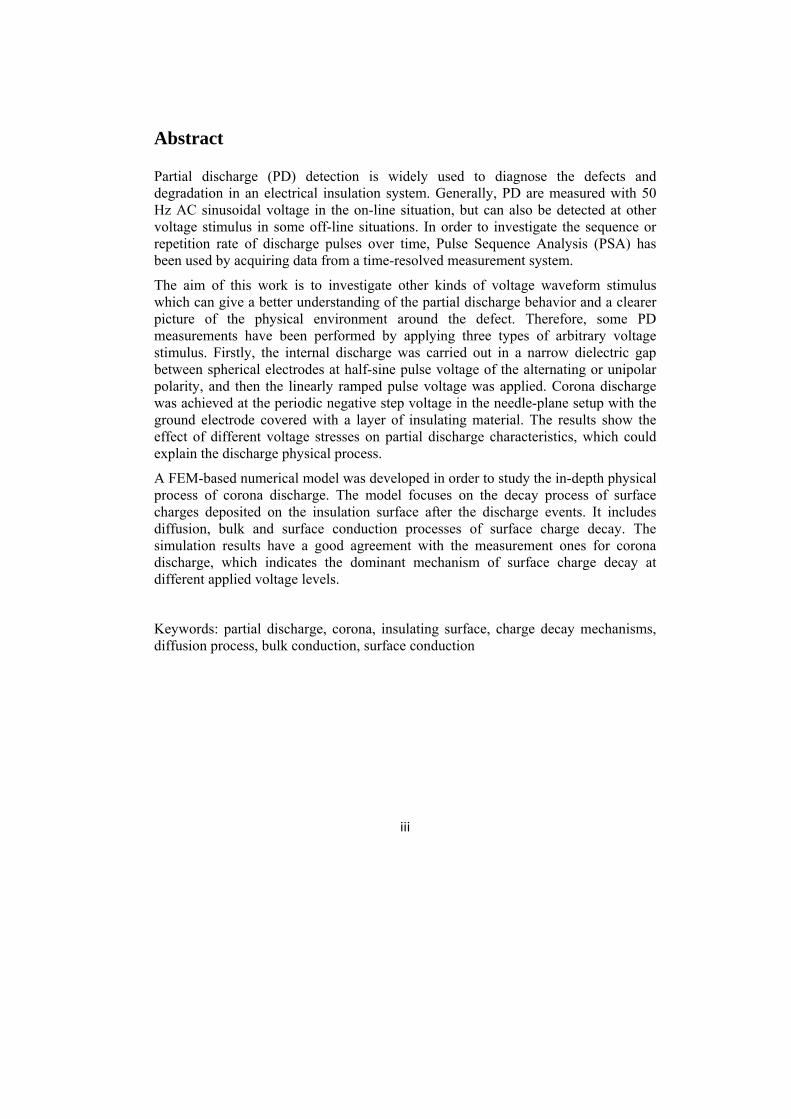
Abstract
Partial discharge (PD) detection is widely used to diagnose the defects and degradation in an electrical insulation system. Generally, PD are measured with 50 Hz AC sinusoidal voltage in the on-line situation, but can also be detected at other voltage stimulus in some off-line situations. In order to investigate the sequence or repetition rate of discharge pulses over time, Pulse Sequence Analysis (PSA) has been used by acquiring data from a time-resolved measurement system.
The aim of this work is to investigate other kinds of voltage waveform stimulus which can give a better understanding of the partial discharge behavior and a clearer picture of the physical environment around the defect. Therefore, some PD measurements have been performed by applying three types of arbitrary voltage stimulus. Firstly, the internal discharge was carried out in a narrow dielectric gap between spherical electrodes at half-sine pulse voltage of the alternating or unipolar polarity, and then the linearly ramped pulse voltage was applied. Corona discharge was achieved at the periodic negative step voltage in the needle-plane setup with the ground electrode covered with a layer of insulating material. The results show the effect of different voltage stresses on partial discharge characteristics, which could explain the discharge physical process.
A FEM-based numerical model was developed in order to study the in-depth physical process of corona discharge. The model focuses on the decay process of surface charges deposited on the insulation surface after the discharge events. It includes diffusion, bulk and surface conduction processes of surface charge decay. The simulation results have a good agreement with the measurement ones for corona discharge, which indicates the dominant mechanism of surface charge decay at different applied voltage levels.
Keywords: partial discharge, corona, insulating surface, charge decay mechanisms, diffusion process, bulk conduction, surface conduction

iv
v
Acknowledgements
I would like to express my gratitude to all those who have helped and supported me during my work.
My deepest acknowledgement goes first and foremost to my supervisor, Assoc. Prof. Hans Edin. His patience, encouragement and professional guidance means a lot to me during the study. This work would not be completed without his support and guidance. I also thank Prof. Rajeev Thottappillil for suggestions regarding my Ph.D. study.
I extend my sincere thanks to my co-supervisor, Dr. Nathaniel Taylor, for his helpful assistance in laboratory experiments, rewarding discussion and correction of my writing. My special thanks to Nadja Jäverberg, who is the first person I turn to for help, and she is really helpful not only in academic area but also in daily life.
I am very fortunate to have a lot of friends within and outside my research group who are supportive and helpful: Mohamad Ghaffarian Niasar, Respicius Clemence Kiiza, Roya Nikjoo, Håkan Westerlund, Seyedali Mousavi, Hanif Tavakoli, Ara Bissal, Jesper Magnusson, giving me a very kind atmosphere to work in.
I am appreciating and enjoying the time together with Chinese friends in Sweden. You make me feel warm in a foreign country.
Also, thanks to Ms. Carin Norberg for financial administration and Mr. Peter Lönn for his continuous support in maintaining computers and software.
The project is funded by the Swedish Energy Agency, Elforsk AB, ABB AB and Swedish Railway Company via the ELEKTRA program, which is gratefully acknowledged. The project is also part of KIC-InnoEnergy through the CIPOWER innovation project.
Last but not least, I am indebted to my parents for their continuous support, encouragement, and endless love to me. I have been far away from them for ten years! I miss them a lot!
Thanks to all of you! Xiaolei Wang Stockholm, December 2012

vi

vii
List of Papers
This thesis is based on the following papers:
I. X. Wang, R. Clemence, and H. Edin, Partial discharge analysis of a narrow dielectric gap with repetitive half-sine pulses, Int. Conf. on Electrical Insulation and Dielectric Phenomena (CEIDP), West Lafayette, Indiana, USA, pp. 481-484, 2010.
II. X. Wang, R. Clemence and H. Edin, Partial discharge analysis of a narrow dielectric gap with repetitive linear ramping pulses, Proc. Nordic Insulation Symposium (Nord-IS 11), Tampere, Finland, pp. 53-56, 2011.
III. X. Wang, M. Ghaffarian Niasar, R. Clemence, and H. Edin, Partial discharge analysis in a needle-plane gap with repetitive step voltage, Int. Conf. on Electrical Insulation and Dielectric Phenomena (CEIDP), Montreal, Canada, pp. 92-95, 2012.
IV. X. Wang, N. Taylor, M. Ghaffarian Niasar, R. Clemence Kiiza, and H. Edin, Surface charge dynamics studied by the temporal evolution of the corona charging current, submitted to IEEE Transactions on dielectrics and electrical insulation, 2012.

viii

ix
Contents
1 Introduction ............................................................................................................ 1 1.1 Background and motivation ......................................................................... 1 1.2 Previous studies ............................................................................................ 2
1.2.1 PD pulse sequence analysis .................................................................. 2 1.2.2 The need for arbitrary voltage application ........................................... 2 1.2.3 PD diagnosis on rotating machines ...................................................... 3
1.3 Aim of this work .......................................................................................... 3 1.4 Thesis disposition ......................................................................................... 4 1.5 Author’s contributions ................................................................................. 4
2 Literature Review .................................................................................................. 7 2.1 Introduction .................................................................................................. 7 2.2 Corona discharge .......................................................................................... 7 2.3 Mechanisms of charge decay ....................................................................... 9
2.3.1 Space charge......................................................................................... 9 2.3.2 Bulk conduction ................................................................................. 10 2.3.3 Surface conduction ............................................................................. 10 2.3.4 Charge diffusion ................................................................................. 11 2.3.5 Gas neutralization ............................................................................... 11
3 Experimental ........................................................................................................ 13 3.1 Measurement system .................................................................................. 13 3.2 Arbitrary waveform .................................................................................... 13 3.3 Test object .................................................................................................. 14
3.3.1 Needle-plane geometry ...................................................................... 14 3.3.2 Cavity in dielectric ............................................................................. 15
3.4 Analysis method ......................................................................................... 16
4 Partial Discharge Experiment Results ............................................................... 17 4.1 Partial discharge in a dielectric gap............................................................ 17
4.1.1 PD analysis with periodic half-sine pulse voltage ............................. 17 4.1.2 PD analysis with periodic linearly ramped pulse voltage .................. 20
4.2 Corona discharge with periodic negative step voltage ............................... 23
5 Corona Discharge Modeling ................................................................................ 27 5.1 Current-voltage characteristic .................................................................... 27 5.2 Lumped circuit modeling of charge decay ................................................. 28
x
5.3 FEM modeling of charge decay ................................................................. 32 5.4 Simulation results ....................................................................................... 33
5.4.1 Diffusion process ............................................................................... 34 5.4.2 Conduction ......................................................................................... 36
5.5 Comparison of measurements to simulation results ................................... 37
6 Summary of Papers .............................................................................................. 41
7 Conclusions and Future Work ............................................................................ 43
Appendix A ............................................................................................................... 45
References ................................................................................................................. 47

1
Chapter 1
Introduction
This chapter starts by describing the background and the motivation of this study, particularly the limitation of present research; it then describes some previous studies of the pulse sequence analysis method (PSA), the benefit of arbitrary voltage application, and partial discharge diagnosis on rotating machines. The focus here is on the aim of this work. Finally, the outline of this thesis and author’s main contribution are given.
1.1 Background and motivation
Electrical insulation systems play a significant role in high voltage apparatus, and their state will determine the safety and stability of the electrical power system. Defects in the insulation system may be created by combined electrical, mechanical, thermal, and environmental stresses during their operation or manufacturing process, resulting in the generation of partial discharges when exposed to a high electric stress, which could lead to a gradual degradation no matter in what kind of insulation system, gaseous, liquid, solid, or a combination of these. Therefore, partial discharge activity is the most common symptom of degradation and overstress in the insulation system of electrical power equipment.
Partial discharge measurement provides a powerful tool for the reliable detection of locally confined insulation defects. The ability to detect, localize and interpret the activity of partial discharges is of fundamental significance in many applications like power cables, rotating machines, transformers etc. It is important to understand the correlations among the measurable parameters of discharge activity and the nature, form and extent of the present degradation for the maintenance and asset management of existing electrical systems. Besides this, understanding the processes and mechanism of partial discharge is of importance to the development of new insulation systems capable of withstanding this stress mechanism [1]. Partial discharge analysis is therefore the most general diagnostic technique for insulation systems.
Partial discharges are commonly measured with 50 Hz AC sinusoidal voltage stimulus in an on-line situation. In off-line situations, it is sometimes possible to apply voltages with another frequency. Low frequencies have therefore been of great interest for a long time, and low frequency partial discharge tests like 0.1 Hz are commonly performed. The ability to vary the frequency at lower frequencies also has

2
a great impact on obtaining much more information about any degradation processes within the equipment. The phase resolved PD activities with variable frequency of the applied voltage have been analyzed in previous projects at KTH [2, 3].
The physics of partial discharges and its relation to the characteristics of the defect is affected by the temporal evolution of the discharges over several time-scales, so the relation between the observations of PDs and its voltage and time dependence is not simple. Therefore, a ‘frequency domain’ approach of excitation and acquisition where the accumulation of PDs into certain phase positions is studied might not be the best method. Therefore, the general aim of this study is to identify an excitation strategy that can give a better picture of partial discharge behavior.
1.2 Previous studies
1.2.1 PD pulse sequence analysis
One of the most common electric PD evaluation tools is the Phase Resolved Partial Discharge Analysis (PRPDA) technique, which gives the q n patterns by analyzing the number and amplitude of the PD pulses with respect to the phase of the applied voltage during a certain time interval [4-6]. The achieved pattern provides some insight into the discharge type and could help to recognize the insulation defects that cause the discharges [7, 8]. However, a particular insulation defect and its specific features may also be reflected in the behavior of the sequence or repetition of partial discharges over time. Sometimes, the accumulated mapping of PDs in an q n pattern may be less suitable to reveal the important information of the relations between different excitations and PD behaviors under certain physical conditions.
Pulse Sequence Analysis (PSA) techniques are well known in PD measurement and assessment; they are based on the evaluation of data sets in which also the sequence of PD events is registered. Each PD activity has memory characteristics which influence the sequence of pulses. The memory is related to the space charges remaining in the proximity of the discharge space after previous discharges [9-11]. Therefore, relating the sequence of PD pulses to defect characteristics is of importance to investigate in order to get a clearer picture of the PD behavior. A lot of research on the characteristics and applications of PSA has been reported in [12-15].
1.2.2 The need for arbitrary voltage application
Partial discharges are non-linear, stochastic, time-variant and hysteretic behavior. They do not appear below a certain inception/extinction voltage, and their pulses occur partly randomly depending on the availability of seed electrons that can initiate the discharge. They are time-variant as they strongly depend on the local conditions, for example, a cavity will change gradually with the exposure to the discharge
3
plasma, which is local ageing. They are hysteretic, for example, discharge activity may continue at a voltage lower than the inception voltage if the voltage is decreased after the stimulus has been above inception for some time.
Therefore, the complexity of the PD phenomena would require that the stimulus is more thoughtful than it has to be for linear systems. For linear systems the same kind of information can be achieved almost independently of how the excitation is performed. However, for dynamic studies of PD we have found that the following ingredients are necessary: to increase and decrease the voltage above and below inception and extinction voltage respectively. Allowing periods without stress, i.e. periods with relaxation might be valuable for obtaining information, which means the arbitrary voltage waveforms are really needed.
1.2.3 PD diagnosis on rotating machines
Rotating machines have a very widespread use in any area of industry. The stator insulating system is one of the most important parts of a high voltage rotating machine with respect to the maintenance and lifetime aspects. Studies show that 56% of the failed machines are caused by insulation damages, and other major types are mechanical, thermal and bearing damages. The two main causes leading to these insulation damages are aging and internal partial discharge, taking 31% and 22%, respectively [16]. There are several kinds of PD sources in insulation system of rotating machines, like slot discharge, end-winding discharge, internal discharge, surface discharge, discharge between bars of different phases, or copper conductor interfaces, and inter-turn discharge. Some important results concerning aging signature and PD behaviors of different defects based on PD patterns for high voltage rotating machines have been reported in [8].
In rotating machines, the insulation usually consists of mica flakes impregnated and bonded with a resin, therefore, this is a highly PD-resistant insulation, able to tolerate considerable internal PD activities (some nC) without having significant effects on the insulation properties. However, degradation of the insulation can develop very quickly if it is exposed to very intensive discharges. Dielectric response and partial discharge measurements on stator insulation have been carried out at KTH in a previous PhD thesis [17].
1.3 Aim of this work
The aim of this project is to investigate other ‘patterns’ of voltage stimulus that can give a better picture of partial discharges and that better can relate the PDs to a physical model. The studies are also performed in conjunction with in-depth physical modeling of PDs, which focuses on the behavior of surface charges deposited on the insulating surface after the discharge events, aiming to improve the models and interpretation rules for PD behaviors.
4
The measurement techniques are intended to be used on the real stator insulation of high voltage rotating machines. The purpose of this work is to improve diagnostic methods that can give significant contributions to the understanding of PD in off-line measurements.
1.4 Thesis disposition
This licentiate thesis is based on the Papers I-IV, and the contents are organized as follows:
Chapter 2 gives short introduction to the partial discharge fundamentals focusing on corona discharge. It then summarizes different mechanisms of surface charge decay, which are bulk and surface conduction, gas neutralization, and diffusion process.
Chapter 3 shows the time-resolved PD measurement system, which was established as a first step in this work. Also the arbitrary waveforms stimulus and the test objects used in this work are introduced.
Chapter 4 presents a summary of the partial discharge measurement results. The internal discharge was carried out in a narrow dielectric gap between spherical electrodes at half-sine pulse voltage and linearly ramped pulse voltage stimulus, separately. Corona discharge was achieved at the periodic negative step voltage stimulus in the needle-plane setup with the ground electrode covered with a layer of insulating material.
Chapter 5 creates an equivalent circuit of a dielectric, as well as a FEM based numerical model based on corona discharge to investigate the dominant mechanisms of the charge decay processes in certain conditions. The measurement results acquired from a needle-plane corona setup are compared with the simulation results from the numerical model.
Chapter 6 summarizes Papers I-IV.
Chapter 7 presents the summary, general conclusions and defines future works.
1.5 Author’s contributions
The author is fully responsible for Papers I-IV. The results in Paper I through IV were developed by the author in collaboration with the Ph.D. students in the Insulation Diagnostics group. The contributions of co-authors are as stated below:
Respicius Clemence Kiiza worked together with the author in laboratory experiments during PD measurements for the results in Paper I and II, and participated in the discussion of some measurement results in Paper III and IV.

5
Mohamad Ghaffarian Niasar participated in the laboratory experiments in Paper III, and joined in the discussion of some simulation results in Paper IV.
The entire work was initialized and supervised by Assoc. Prof. Hans Edin, with Dr. Nathaniel Taylor as co-supervisor.

6
7
Chapter 2
Literature Review
This chapter reviews previous studies on Warburg’s law and current-voltage characteristic equation of corona discharge, as well as different decay mechanisms of surface charges deposited on the insulating surface, such as bulk conduction, surface conduction, gas neutralization, and surface- and bulk diffusion processes.
2.1 Introduction
The investigation of PD has played an important role in electrical apparatus design and long-term performance during the last decades. Although PD does not cause an immediate breakdown of insulation, every discharge event could cause a slow deterioration of the material by the energy impact of high energy electrons or accelerated ions, causing many types of discharge-induced physical-chemical reactions to the material, e.g. temperature increases, reactions and wall erosion, space charge injection. Therefore, with the development of discharges, the insulation system could be damaged gradually, and then eventually the complete failure may happen.
The reason for the partial discharge being initiated could be a nonuniform electric field or an inhomogeneous material between the electrodes. PD includes a wide group of classic sources: (a) corona discharges occurring in air or other gaseous dielectrics at a sharp point, corner or protrusion of an electrode; (b) surface discharges appearing at the boundary of different insulation materials where there is a high electric field component parallel to the dielectric surface; (c) dielectric-barrier discharge is widely used for deliberate production of PD, where plasmas are desired for their optical and chemical effects [17]; (d) internal discharges occurring on locations of solid or liquid insulation where the dielectric strength is lower than that of the surrounding dielectric, such as voids or impurities; (e) continuous impact of discharges in solid dielectrics may cause erosion of the walls of the cavities, forming electrical treeing.
2.2 Corona discharge
Corona is a self-sustained discharge which occurs around the electrode of small radius of curvature in gaseous dielectrics; its electrical characteristics are strongly dependent on the polarity of the active electrode. Corona is detected at lower voltage when the point electrode is negative rather than positive.

8
The steady point-plane corona discharges can be described by the characteristics of Warburg’s law and the corona current-potential equation. Warburg’s law is an empirical relation of corona current density distribution on a conducting plane given as
0m
sJ J cos (2.1)
which shows the current density distribution sJ over the plane electrode as a
function of the angle whose vertex is at the needle electrode, as shown in Figure 2.1. 0J is the current density directly beneath the discharge point. Generally, 5m for 60o has been found to be in harmony with modern empirical data [18-20].
Also, 2 2cos h r h , r is the distance from the center of the plane and h is the effective distance from the needle point to the plane.
05cos θsJ J
0J
r
h
Figure 2.1 A typical needle-plane corona geometry showing the Warburg current density
distribution on conducting plane
After the corona discharge starts, the current then rises with the increasing voltage, following a current-voltage characteristic equation. Several empirical formulas are suggested to describe this characteristic, given as [20-22]
1 0( )I K V V V (2.2)
or
22 0( )I K V V (2.3)
where 0V is the corona inception voltage; 1K and 2K are constants that depends on
the geometry. An approximate estimate of the limiting surface potential PV can be

9
made when an insulating material is placed on the plane. Every corona discharge deposits a certain amount of charges on the dielectric surface, leading to a charge accumulation, and then a potential on the symmetry axis PV can be built on the surface. So the current-voltage equation is modified based on equation (2.2) with the same value of K as the case without the material, as mentioned in [22]
0( )( )P PI K V V V V V (2.4)
2.3 Mechanisms of charge decay
2.3.1 Space charge
The presence of space charge plays a major role in promoting acceleration of ageing processes and bringing an insulation system to early failure under electrical stress [23]. The failure can be due to the space charge accumulation, which could affect the electric field inside the insulation.
When an AC voltage is applied to a cavity inside the dielectric, the electrons and the ions start to move towards the anode and the cathode respectively, forming an electric field with the opposite direction of the background field, which contributes to extinguishing the discharge event. After the first discharge is completely done, an equal amount of positive and negative charges are deposited on the surface of the surrounding dielectric material. These deposited charges provide a great effect on the following discharge behavior, increasing or decreasing the local electric field at the time of the next discharge happening, depending on the polarity of the applied voltage. Thus, after one discharge has taken place, the next ones are governed not only by the background field, but also by the electric field generated by the space charge deposited by any previous discharge activities. The repetition of PD pulses depends on the recovery of the electric field inside the cavity, which is controlled by the presence of charges on the surface of the dielectric material through Poisson’s equation.
During the time interval between two consecutive discharges, space charge deposited on the surface of the dielectric may decay following different physical origins such as bulk conduction [24-27], surface conduction [24-26, 28, 29], neutralization by gas ions [24, 30, 31], trapping in surface states [32, 33], and diffusion processes [34-38]. The impact of the above physical mechanisms on PD activities is determined by the time constant of the charge relaxation process and the rate of change of the electrical field inside the cavity. The decay rate of the surface charge can have a significant impact on the field recovery, and then on the maximum PD amplitude and repetition rate, thus impacting on the diagnostic approach based on PD pattern identification. Therefore, different kinds of voltage waveform stimulus have been used to

10
investigate the PD behaviors due to the charge movement in the space under different electric fields [39, 40].
Charge decay on insulating materials can be detected by the measurements of electric field, charge densities and surface potential [41-45]. A lot of studies have been carried out to investigate the surface charge decay characteristics, such as the influence of different material [25, 45, 46], geometrical arrangement [47], relative humidity [34, 48, 49], temperature [34, 41], and ambient gas [46]. Moreover, the surface charge decay time of the different material samples has been evaluated by [45]. It was reported that the initially bell-shaped surface charge density distribution can remain with the same shape during the decay [25], may change into a crater-like shape of charge distribution [25, 44], or may spread along the surface [34].
2.3.2 Bulk conduction
Bulk neutralization of surface charge can be due to the effect of dipolar polarization processes [26, 50, 51], intrinsic conduction of the material [24] or charge injection into the bulk [26, 44]. Assume an insulating material with a constant permittivity and a constant intrinsic conductivity V , which gives a very simple surface charge
decay model. The time dependent current density ( , )VJ r t
through the material
volume is exponentially decaying with time [24]
0( , ) ( , ) exp( )VJ r t J r t t
(2.5)
where 0J is the current density at 0t and the time constant can be given by
V (2.6)
Generally, the surface charge decay due to bulk conduction can be characterized firstly by exponential decay with time after a specific polarization time, and secondly by a uniform change of surface charge distribution at each position on the surface [30].
2.3.3 Surface conduction
Surface conduction refers to the charge transport along the insulating surface because of the tangential electric field. The lateral motion of charges on the dielectric surface strongly depends on the surface condition, such as temperature, relative humidity, contamination, etc. In the case of an ohmic conductive surface, it can produce an exponential potential decay, which is a typical behavior of surface conduction [26, 52]. The surface current density ( , )SJ r t
on the insulating surface is given by
, ,S t SJ r t E r t
(2.7)

11
where ( , )tE r t
is the tangential component of the electric field along the insulating
surface and S is the surface conductivity [24].
A sensitive method to measure the surface conductivity of insulators is given in [53]. The model based on the equivalent circuit of bulk capacitance and surface resistance shows the time dependent behavior of current flowing on the surface following
1 2( )I t t . The surface potential decay caused by the ohmic conduction of both the surface and the volume of the sample has been investigated in [28]. The decay of charges deposited on the wall of a gaseous void after PD activities due to surface currents at the void wall has been studied analytically in [54].
2.3.4 Charge diffusion
Diffusion refers to the motion of species tending to spread from regions of high concentration to regions of low concentration. It can be affected by the free volume, the humidity, and the temperature.
The typical example of lateral charge spreading on the dielectric surface has been given by [34], in which it is reported that the charges deposited on the surface of PET from a corona discharge move laterally by a diffusion law. However, the results in [55] show that the surface charge decay may originate from a dielectric polarization followed by a slow diffusion of charges in the bulk of the polymer, without any observation of charge spreading on the film surface. A charge transport theory is also presented, which allows interpretation of the data especially for the initial phase of surface charge decay [37], and also gets the accurate determination of both the diffusion coefficient and the layer of surface charge [38]. The diffusion coefficient D in terms of mobility is given as [36-38]
eD kT (2.8)
where k is Boltzmann’s constant and T is temperature. The diffusion process could be more important than the charge distribution caused by the electric field when the particle concentration is higher, which means at short times after the charge deposition [28].
2.3.5 Gas neutralization
The contribution of the surrounding gas to charge decay can be treated as neutralization by counter ions resulting from natural background radiation [24, 30], or as gas conductivity which depends on the applied electric field [56, 57].
It is suggested in [24] that the contribution of gas ions to the surface charge decay has to be considered as a kind of current source rather than by the assumption of a constant gas electrical conductivity. Some important parameters for the mechanism of charge neutralization by gas ions are the rate of ion pair generation, the ion-ion

12
recombination coefficient, and the effective neutralization volume limited by the electric field strength. The gas ions produced by an electric field follow the electric field lines until they recombine or reach the insulation surface. Thus, the effective gas volume and the field distribution in this volume could also affect the current in the insulation material. This volume is called effective neutralization volume or capture volume, in which the field strength is high enough for the ions to reach electrically charged surface [24, 30].
The average ion pair generation rate dn dt can be assumed to be in the order of 10 ion pairs (IP) cm-3s-1. Assuming a constant ion-pair generation rate under zero field condition and neglecting diffusion process, the equilibrium ion density en is given by [24]
er
dn dtn
k (2.9)
where rk is the ion-ion recombination coefficient, with the value of 61.5 10rk cm3s-1 at 0.1 MPa and 20 ºC in atmospheric air, then an average value of ion density can be estimated.

13
Chapter 3
Experimental
This chapter describes the time-resolved partial discharge measurement system, and the voltage application based on three types of arbitrary waveforms. It also describes the test object used in this work. Finally, the Pulse Sequence Analysis (PSA) method is introduced.
3.1 Measurement system
The time-resolved PD measurement system consists of an Agilent 33120A function generator, a TREK 20/20 high-voltage amplifier, a coupling capacitance, a detection impedance, a Yokogawa DL750 ScopeCorder and a computer, as shown in Figure 3.1.
The high voltage was generated by the function generator and then amplified by the high-voltage amplifier. The coupling capacitance KC was 250 pF (two 500 pF LCC
ceramic capacitors in series), which was in series with the detection impedance tZwith a resistance of 1 kΩ. The partial discharge pulses were acquired with the ScopeCorder, with 12-bit A/D resolution, a sampling rate of 10 MS/s, and a deep memory of 250 MS, which allowed long time pulse sequence analysis.
Figure 3.1 Schematic of time-resolved PD measurement system
3.2 Arbitrary waveform
The voltage stimulus used here was based on three kinds of arbitrary waveform:

14
(a) Periodic half-sine pulses, which were half-sine pulses of variable duration 1T , and before the consecutive half-sine pulse, which may be of the alternating or unipolar polarity, a pause period of duration 2T was introduced to influence the relaxation of space charges from previous discharges, as shown in Figure 3.2 (a). The results are shown for the case of 1 10 msT (corresponding to 50 Hz) and pause time 2T varying
from 0 (pure 50 Hz) to several times 1T .
(b) Periodic linearly ramped pulses, which were an alternating voltage with piece-wise linear increasing and decreasing parts. The time-to-peak of the rising part of each polarity had a variable duration of 1T , thereafter followed a linear falling voltage
with the variable duration 2T . There was a pause time 3T that can be set arbitrarily long between positive and negative pulses, as shown in Figure 3.2 (b). The results shown are for the fixed duration of 1 5 msT (resemblance to 50 Hz), 3 0T , and the
falling time 2T varied from 5 ms to 500 ms to affect the decay of space charges deposited on the insulating surface.
(c) Periodic negative step pulses, which were a sequence of negative step voltage pulses alternating between zero and a level above partial discharge inception. The duration of the voltage periods 1T and the pause at zero voltage 2T can be varied, as shown in Figure 3.2 (c). This work is limited to the results for the case of
1 100 msT and 2 10 sT .
3.3 Test object
The test objects were a dielectric gap between spherical electrodes, and a needle-plane geometry with the ground electrode covered by a layer of dielectric. The insulating material used here was a polycarbonate layer with the thickness of 0.25 mm.
3.3.1 Needle-plane geometry
A circular plane copper electrode, having a diameter of 82 mm and a thickness of 12 mm, was used as the ground electrode. The sheet of insulating material covering the ground electrode was a layer of polycarbonate plate with a thickness of 0.25 mm and an area of 85 mm × 95 mm. A stainless steel needle with a tip radius of 15 μm was placed in the center of the top plane. The needle length was 2.9 cm and the distance between the needle tip to ground electrode was 1 cm.

15
(a)
(b)
(c)
Figure 3.2 Arbitrary voltage stimulus used in this work: (a) Half-sine pulse with alternating or unipolar polarity, (b) Linearly ramped pulse, (c) Negative step voltage pulse.
3.3.2 Cavity in dielectric
Figure 3.3 shows a schematic of the test object between spherical electrodes, which is an insulated disc-shaped cavity in polycarbonate. Three polycarbonate plates, each having a thickness of 0.25 mm, were pressed together. A square gap of the side 40
t
U(t)
T1 T2
T1 T2t
U(t)

16
mm was made in the middle plate to create a dielectric gap. The gap distance was 0.25 mm. The cavity size was larger than the electrode diameter to avoid the effect of discharges on the vertical cavity wall.
Before each measurement at a new applied voltage, the test object was allowed to relax by grounding the material to remove all the charges on the surface of the material.
Figure 3.3 Schematic of test object with dielectric gap between spherical electrodes.
Almost rotational symmetry. Measures are given in millimeters.
3.4 Analysis method
The sequence of the partial discharge events contains the information for PD analysis. The main data characteristics in PSA analysis are the detected PD pulse apparent charge, q , the applied voltage, u , at the time of that discharge and the relative time
of occurrence of the PD pulse, t . In principle, the sequence of this matrix ( , , )i i it q uis sufficient to describe a partial discharge process. A large number of points have been acquired due to the long time measurement at a high sampling rate, especially for the longer pause period case, but what we are really concerned about is only the data describing the PD pulse. Therefore, it was necessary to dilute the data recorded from the ScopeCorder before further processing. Thus, a Matlab program was used to pick out the peak values of PD pulse amplitude over a discrimination or ‘filtering’ level. This level should be selected as small as possible in order not to miss some small discharge pulses.

17
Chapter 4
Partial Discharge Experiment Results
The partial discharge measurements were performed under three types of arbitrary waveform stimulus. Firstly, the partial discharge was measured in a narrow dielectric gap at half-sine pulse voltage of the alternating or unipolar polarity, after that, the linearly ramped pulse voltage was applied to the same test object. Then corona discharge was measured at the periodic negative step voltage in the needle-plane setup to investigate the influence of surface charges deposited on the insulating material on the discharge activities.
4.1 Partial discharge in a dielectric gap
4.1.1 PD analysis with periodic half-sine pulse voltage
The first arbitrary waveform application was based on half-sine pulse voltage of the alternating or unipolar polarity with the pause period between the two consecutive pulses, shown in Figure 3.2 (a), which was used in a narrow dielectric gap of 0.25 mm; the geometry is shown in Paper I. The influence of the variable zero-voltage relaxation time was studied based on the time-sequence of discharge pulses.
The PD inception voltage incU at 50 Hz normal sinusoidal voltage was 4.4 kV. The
PD activities were measured at applied voltage amplitude of 6 kV at 1 10 msT , with
the pause time 2T set to 0, 1T , 15T and 110T . The measured PD patterns together with the applied voltage waveform in these conditions can be found in Paper I. Figure 4.1 shows the zoomed discharge pattern at one cycle of the applied half-sine voltage at two extreme situations.
The periodic positive half-sine voltage pulses ware applied in order to see the behavior of a unipolar excitation, with the measurement results also shown in Paper I. The PD inception voltage incU in this case of 50 Hz positive sine voltage was 8.8 kV, which was higher than in the alternating polarity case, and the PD activities were measured at applied voltage amplitude of 10 kV. Figure 4.2 shows the zoom-in discharge pattern for two cycles of applied positive half-sine voltage in two extreme situations. The voltage waveform shown here is recorded from the function generator, and the real applied voltage value should be amplified by 2000. The relative voltage position of PD occurrence is marked on the waveform.

18
(a)
(b)
Figure 4.1 PD pattern measured at one cycle of the applied half-sine voltage of 6 kV at
1 10 msT and different 2T values: (a) 0 ms, (b) 100 ms.
0.005 0.01 0.015 0.02-3
-2
-1
0
1
2
3
Time [s]
Par
tial D
isch
arge
Vol
tage
[V
]
0.15 0.2 0.25 0.3-3
-2
-1
0
1
2
3
Time [s]
Par
tial D
isch
arge
Vol
tage
[V
]

19
(a)
(b)
Figure 4.2 PD measured at two cycles of the applied positive half-sine voltage of 10 kV at 1 10 msT and different 2T values: (a) 0 ms, (d) 100 ms.
From the partial discharge patterns presented in Paper I and the ones in Figure 4.1 and 4.2, the following are observed:
Almost no discharges occur during the pause period in both unipolar and bipolar half-sine applied voltage, an effect that shows that the space charge field by itself rarely can generate a discharge.
0.01 0.015 0.02 0.025-1
0
1
2
3
4
5
Time [s]
Par
tial D
isch
arge
Vol
tage
[V
]
0.05 0.1 0.15 0.2-1
0
1
2
3
4
5
Time [s]
Par
tial D
isch
arg
e V
olta
ge [V
]
20
In the case of bipolar half-sine voltage across the cavity, the maximum charge grows with the pause time. This effect may be attributed to a reduction of free electrons that can start the avalanche, i.e. the numbers of available seed electrons vanish during the pause period and cavity tends to its virgin state again.
In the case of unipolar positive half-sine voltage across the cavity, the discharge pattern formed has positive discharges during rising voltage, and negative discharges during falling voltage. This discharge pattern seems to be rather independent of the pause time 2T .
4.1.2 PD analysis with periodic linearly ramped pulse voltage
The next study was to investigate an arbitrary voltage waveform that had constant rate of changing, i.e. a triangular voltage. The voltage application here was based on the fixed duration of a linear increasing part followed by a linear decreasing part that was varied to affect the decay of space charges deposited on the insulating surface, as seen in Figure 3.2 (b).
The PD inception voltage incU was about 6.6 kV in the narrow dielectric gap at 50 Hz
triangular voltage ( 1 2 5 msT T ). The PD activities were measured at an applied
voltage amplitude of 8 kV (1.2 incU ) at a linear rise time 1 5 msT , with the linear
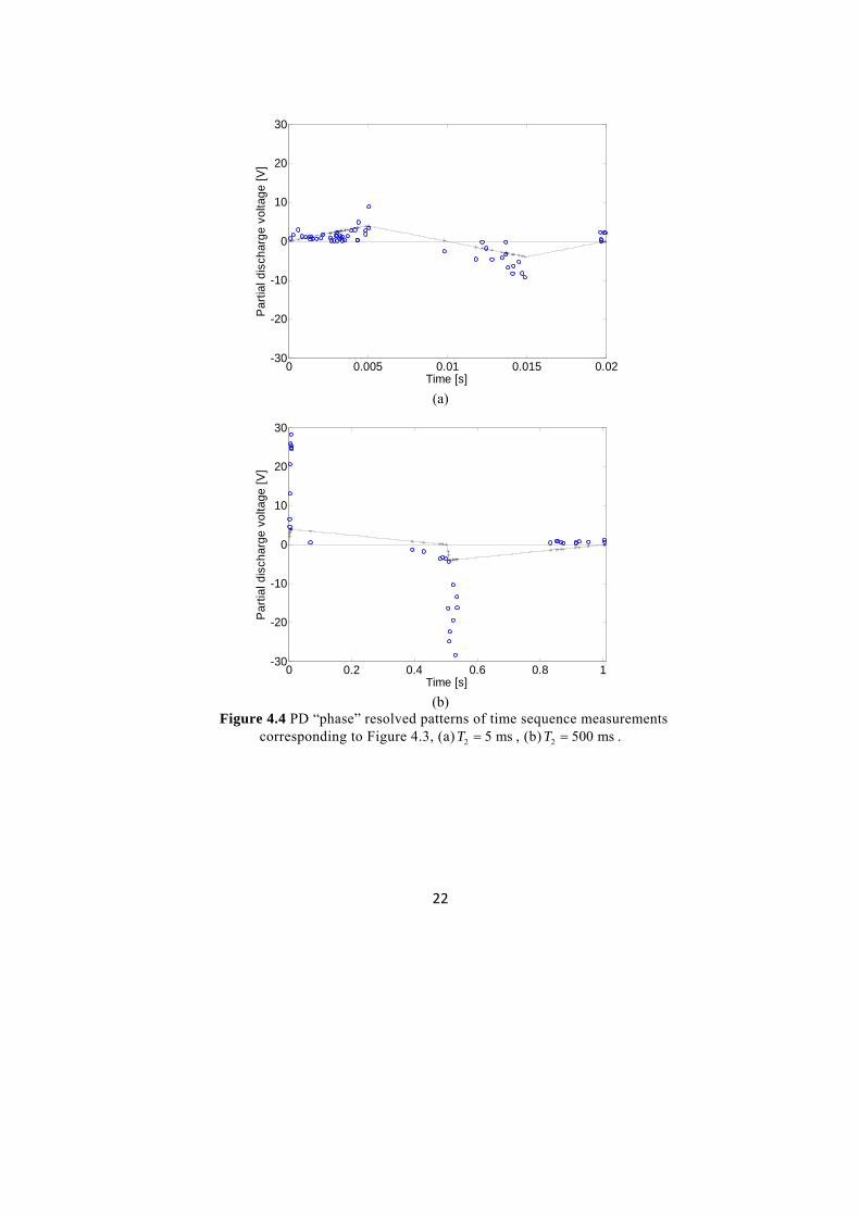
fall time 2T set to 1T , 12T , 110T , 120T , and 1100T . Figure 4.3 shows two examples of the zoom-in discharge pattern for one cycle of applied triangular voltage; more results can be found in Paper II. In order to get a more aggregated view of PD behaviour, a PD “phase” resolved pattern was made by transferring all the PD pulses recorded during at least ten cycles into a single reference cycle of the applied voltage, as shown in Figure 4.4.
From the observation of discharge patterns in Figure 4.3 and 4.4, the partial discharges that occur during the period of 1 5 msT are strongly affected by
increasing the duration of the decay voltage period 2T . Here it can be observed that:
The PD pulse amplitude grows significantly with the increasing time 2T , and the maximum pulse voltage increases from 10 V up to 30 V.
The total charge per half cycle is the total charge in all the measured periods divided by the number of measured cycles. It is clear that the total charge per half cycle has a remarkable trend with the variable 2T period for both the positive and negative polarity. Figure 4.5 shows that the total charge per half cycle could be fitted to a function
1 22 2( ) 1300 230 ( )f T T (4.1)

21
This power law dependence with the exponent 1 2 is a common signature of a time-dependent process that is controlled by diffusion process. A speculation is that it is due to charge diffusion into the bulk which implies that with increasing 2T more charge is trapped in the bulk below the surface. After polarity reversal the field from these charges may imply that the discharge takes place at an increased field and therefore become larger.
(a)
(b)
Figure 4.3 PD measured during one cycle of the applied linear ramping voltage of 8 kV at 1 5 msT and different 2T values: (a) 2 5 msT , (b) 2 500 msT .
0 0.005 0.01 0.015 0.020.02-30
-20
-10
0
10
20
30
Time [s]
Par
tial d
isch
arg
e vo
ltag
e [V
]
0 0.2 0.4 0.6 0.8 1-30
-20
-10
0
10
20
30
Time [s]
Par
tial d
isch
arge
vol
tage
[V
]
22
(a)
(b)
Figure 4.4 PD “phase” resolved patterns of time sequence measurements corresponding to Figure 4.3, (a) 2 5 msT , (b) 2 500 msT .
0 0.005 0.01 0.015 0.02-30
-20
-10
0
10
20
30
Time [s]
Par
tial d
isch
arg
e vo
ltag
e [V
]
0 0.2 0.4 0.6 0.8 1-30
-20
-10
0
10
20
30
Time [s]
Par
tial d
isch
arge
vol
tage
[V
]

23
Figure 4.5 Total charge per half cycle behaves as a function of the square root of 2T .
4.2 Corona discharge with periodic negative step voltage
To motivate the study in a better way, one simple voltage waveform was applied to the simple needle-plane geometry. The voltage application here was based on the periodic negative step voltage with 1 100 msT and 2 10 sT , shown in Figure 3.2 (c). Note that the voltage application in this part is the negative step voltage and all the values shown in the measurement data are the absolute value of the negative one.
The total number of corona pulses was first measured in the needle-plane geometry. Figure 4.6 shows the evolution of corona pulses ( )N t at different voltage levels with
a step voltage period of 1 100 msT . Figure 4.7 shows the evolution of corona pulses
( )N t at the eight periodic negative step voltage in one voltage level of 4.8 kVV . The current-voltage relation from the measurement can be fitted to the equation
20 1 0( ) ( )N t K V V T q (4.2)
where the inception voltage can be calculated by the data in Figure 4.6, with the value of 0 3 kVV . The constant value of K is about 12 22.65 10 (C / (V s))K .
The charge of each corona pulse was approximated 0 50 pCq for this needle-plane setup.
To study the effect of insulating material on the discharge behavior, a layer of dielectric sample was placed on the top of the ground electrode into the same needle-plane geometry. The evolution of cumulative corona pulses during eight consecutive
0 100 200 300 400 5001000
2000
3000
4000
5000
6000
7000
Duration of T2 [ms]
Par
tial D
isch
arge
Char
ge [
pC]
Absolute value of total negative charge per half cycleTotal positive charge per half cycleCurve fitting

24
cycles with different applied voltage levels was investigated; the results can be found in Paper III. The corona pulse behavior at a lower and a higher voltage level are shown in Figure 4.8. The inception voltage is higher than that without dielectric
0 3.2 kVV , which is somewhat unexpected as the dielectric layer should increase the field around the needle tip at least slightly.
Figure 4.6 The evolution of corona pulses at the different applied voltage levels
Figure 4.7 The evolution of corona pulses during the consecutive eight periods of the applied voltage
0 0.02 0.04 0.06 0.08 0.10
2000
4000
6000
8000
10000
12000
14000
16000
Time [s]
Nto
t(t)
V=-4.2kVV=-4.4kVV=-4.8kV
0 0.02 0.04 0.06 0.08 0.10
2000
4000
6000
8000
10000
12000
14000
16000
Time [s]
Nto
t(t)
1st cycle2nd cycle3rd cycle4th cycle5th cycle6th cycle7th cycle8th cycle

25
(a)
(b)
Figure 4.8 The evolution of corona pulses at eight consecutive cycles of different applied voltage with dielectric on the surface of the ground electrode: (a) 4 kV, (b) 6.8 kV.
0 0.02 0.04 0.06 0.08 0.10
100
200
300
400
500
Time [s]
Nto
t(t)
1st cycle2nd cycle3rd cycle4th cycle5th cycle6th cycle7th cycle8th cycle
0 0.02 0.04 0.06 0.08 0.10
2000
4000
6000
8000
10000
12000
Time [s]
Nto
t(t)
1st cycle2nd cycle3rd cycle4th cycle5th cycle6th cycle7th cycle8th cycle

26
From the comparison of cumulative number of corona pulse behavior in the two cases mentioned above, the influence of the dielectric layer covering on the surface of the ground electrode was investigated. From Figure 4.6 through Figure 4.8, it can be observed that:
The cumulative corona pulse events increase linearly with the increasing time for every applied voltage level, which indicates that corona activities follow a constant repetition rate ( )dN t dt , as shown in Figure 4.5.
Without the dielectric on the ground electrode, the cumulative corona pulse number during the consecutive applied voltage period follows the same trend, shown in Figure 4.6, which means that the space charges originating from the needle tip go to the metal plane quickly and the discharge space tends to its virgin state again. Therefore, the charges in the space cannot affect the following corona behavior obviously in this situation.
The 1( )N t T behavior at a lower applied voltage in Figure 4.7 (a) shows that the cumulative corona pulse number at the first cycle of the applied voltage is much higher than the other cycles, and it increases exponentially until levels off after 20 ms. This saturated level means the discharge activity goes down. It seems that the surface charges deposited by corona discharge stay on the surface of the dielectric, which decelerates the discharge activity, and even stops it if the duration of the applied step voltage is increased above 100 ms.
When the voltage is significantly higher than the inception voltage, the total discharge number behaves almost linearly for every cycle with different delay time after the voltage is switched on, as it can be seen in Figure 4.7 (b). This might indicate that the space charges follow a different decay mechanism at the higher applied voltage.

27
Chapter 5
Corona Discharge Modeling
Based on the observation of partial discharge behavior from Chapter 4, a lumped circuit model of a dielectric and a FEM based numerical model of corona discharge were developed here to motivate the study of surface charge decay. Some surface charge decay mechanisms including diffusion processes and conduction were investigated in certain conditions. Finally, the measurement results acquired from needle-plane corona setup are compared with the simulation results from the numerical model.
5.1 Current-voltage characteristic
Empirical formulas are suggested to describe the current-voltage characteristic, as mentioned in Chapter 2.2. The measurement data of corona discharge given in Figure 4.6 follow the relation as
20( )I K V V (5.1)
With the assumption that the single discharge pulse does not have a cumulative effect on the background electric field, then every corona discharge event from the needle tip should give almost the same amount of charge 0q . Therefore, the cumulative
corona charge ( )Q t during discharge activities is
0( ) ( )Q t q N t (5.2)
where ( )N t is the cumulative number of corona pulses from the start. The average
corona current CI is then obtained by
0
( ) ( )C
dQ t dN tI q
dt dt (5.3)
Every corona discharge deposits a certain amount of charges on the dielectric surface, leading to a charge accumulation, and a corresponding increase of the surface potential. The surface potential on the symmetry axis is PV . This causes reduction of
the voltage difference across the gap to PV V [22], leading to the current-voltage relation with the same constant value of K , given as
20( )C PI K V V V (5.4)

28
As charges from corona build up on the insulating surface, PV increases. Therefore,
the corona current CI decreases, and even becomes zero if PV builds up high enough. From equation (5.3) and (5.4), the relation between the total number of discharge pulses and the applied voltage can be achieved.
5.2 Lumped circuit modeling of charge decay
An equivalent circuit is proposed to describe the surface conduction and bulk properties of dielectric on the plane, seen in Figure 5.1. Assume the discharge area as a circular region, as well as the dielectric.
Figure 5.1 Lumped-circuit model of a dielectric
Each ring-shaped element of the bulk has a capacitance and resistance given by
2
1 0 1
2 20 1( )
r
i r i i
C r d
C r r d
(5.5)
21 1
2 21( )i i i
R d r
R d r r
(5.6)
Each ring-shaped element of the surface has a resistance given as
1 1 1
1
2
( ) 2s s
si s i i i
R r r
R r r r
(5.7)
where ir is the external radius of the ith ring, d is the thickness of the dielectric, and s are the bulk and surface resistivity of the dielectric material, respectively. We
have the voltage at node i

29
( )i iV V r (5.8)
The current balance at node 1 given by
1 1 2 11 1
1 1s
dV V V VI C
dt R R
(5.9)
and the current at general node i (1 i N ) is
1 1
1
i i i i i ii i
si si i
V V dV V V VI C
R dt R R
(5.10)
where iI is the corona current element at node i . At the last node, 1N , the
resistive layer is assumed to reach ground, therefore, 1 0NV . This discrete formulation will yield an equation system of the form
i i
dV MV b
dt (5.11)
where the matrix M and vector b can be found in Appendix A.
It is assumed that the Warburg law is even true for the insulating surface, as shown in Figure 5.2, so that the radial dependent current density is considered as the initial distribution on the surface. The corona current element at node i is
50 cos 2iI J rdr (5.12)
where 2 2cos h r h , with r the distance from the center of the plane and h is the distance from the needle point to the plane.
The total current is derived by
500cos 2
L
CI J rdr (5.13)
which gives a total current expressed as function of gap length h and 0J
52
0 2 2 3 2
2
3 ( )C
hI J h
L h
(5.14)

30
r
Figure 5.2 A typical needle-plane geometry showing Warburg’s law on insulating plane
When L , we have
20
2
3CI h J
(5.15)
All the current iI coming into each node should be equal to the total current I
5 50
22
0
cos 2 3cos23
i C C
J rdr rdrI I I
hh J
(5.16)
Then corona current at node i can be given by
52 2
2 2 2 5 2
3( ( 1) ( ) )
2 ( )i C
hI I r i r i
h h r
(5.17)
with the corona current source CI from equation (5.4). A matlab program was made based on equation system (5.11) to investigate the surface potential and the cumulative number of discharge pulses. Figure 5.3 shows the behavior of the cumulative number of corona pulses at the applied voltage of 4 kV with the inception voltage of 3.2 kV. Figure 5.4 gives the corresponding surface potential developed on the dielectric of each node in the equivalent circuit. The specific parameters in this example are the bulk resistivity 1210 m , the surface resistivity 1210 ms ,
the thickness and the radius of material 0.25 mmd , 5 cmr . The number of nodes is 100i .

31
Figure 5.3 The cumulative number of corona pulses obtained from the lumped-circuit model
Figure 5.4 Surface potential at each node in the lumped-circuit model of a dielectric
0 0.02 0.04 0.06 0.08 0.10
50
100
150
200
250
300
350
400
Time [s]
Nto
t(t)
0 0.02 0.04 0.06 0.08 0.10
100
200
300
400
500
600
700
800
Time [s]
Sur
face
pot
entia
l [V
]
32
5.3 FEM modeling of charge decay
The lumped-circuit model of a dielectric is an ‘engineering’ model to consider the insulating material as series of capacitance and resistance. On the other hand, a more physical model is presented here to investigate the conduction and diffusion processes in charge decay model based on Possion’s equation and continuity equation, as described briefly below. The gas neutralization mechanism is not considered in the charge decay model because its small current can be neglected compared with the corona current source; more details can be seen in Paper IV.
Assume the surface and bulk conductivities built-up are due to the deposited charges by themselves, and only one type species of negative ions is considered in the model. Thus, the bulk as well as the surface conductivity i can be expressed by the relation
i i ien (5.18)
where in is the concentration of ions, i is the mobility of ions, e is the charge of each ion. The ionic current density is then given by
Cond i i V J E (5.19)
with
2i in e D kT (5.20)
being the Einstein-Nernst relationship for the diffusion coefficient D in terms of mobility, and D is taken here to be constant for simplicity [36-38]. k is Boltzmann’s constant and T is temperature. The mobility is given in equation (2.8).
The potential will follow Poisson’s equation in the region with the charge density term included as the source term
2 ienV
(5.21)
The current density can be removed from the equation (5.19) by the continuity equation
0 Cond t
J (5.22)
Then we have
33
2
( )( ) ( )
( )
iCond i i
ii i i i i i
enV en V
t tn
n V n V n Vt
J (5.23)
Expressing everything in in by using equation (5.21) will then give
2i ii i i
nn V en
t
(5.24)
Besides this the charge motion due to diffusion could happen when there is a concentration gradient. Thus, the flow of charges is then
flow i Diff if D n eD n J (5.25)
The diffusion current component obeys the same rules
0Diff t
J (5.26)
Then we get
2
( )( )
iDiff i
ii
eneD n
t tn
D nt
J (5.27)
This current component must then be added to equation (5.24) and one comes down to
2 2i ii i i i
nn V en D n
t
(5.28)
This equation can be solved to give the behavior of how the charges deposited on the insulating surface decay due to the conduction and diffusion mechanisms.
5.4 Simulation results
The numerical simulation presented here is based on Electrostatics and PDE models in COMSOL 4.2 to simulate the influence of the charge decay mechanisms shown in equation (5.28), including diffusion process and conduction. Two important parameters achieved from simulation results are studied, which are the cumulative number of corona pulses and the surface potential built-up on the insulating surface.

34
The geometry of insulating material used here is shown in Figure 5.5. This is a 2D axisymmetric model of an insulating disk with radius of 50 mm and thickness of 0.25 mm. The top 10% of the thickness is considered to represent the surface layer, and the lower part is the bulk of material [38]. All the boundary and domain settings are also shown in Figure 5.5.
0.025 mm0.25 mm
Ground
50 mm
Zero charge
εr =1
εr =2.9
Axial Symmetry Zero charge
P
Figure 5.5 The geometry of insulating material used in COMSOL
The corona current injected into the surface layer is considered as the source term of the PDE model. The source in the electrostatics model is space charge accumulation on the insulating surface, represented by the space charge density of ie n on the top
domain, where in can be obtained from the PDE model. The Warburg relation is also considered as the initial distribution on the insulating surface. More details can be seen in Paper IV. All the simulations are carried out up to 0.1 s in order to compare with the measurements.
Regardless of the relation between the diffusion coefficient and the mobility shown in equation (2.8), the impact of individual mechanisms on the behavior of the total PD number is treated separately by applying every coefficient to the same initial settings in either the surface or bulk of the insulating material. Surface diffusion and conduction is 1D and 1 ; bulk diffusion and conduction is 2D and 2 . The constant
value of K used here is from the measurement with 12 22.65 10 (C / (V s))K .
5.4.1 Diffusion process
Diffusion is considered based on the equation (5.27) in the case of the applied voltage of 4 kV. The same value of diffusion coefficient 8 2 -1
1 2 10 m sD D was

35
inserted into the surface and bulk domain of the insulating material, separately. The characteristics are shown in Figure 5.6 and 5.7. It is found that bulk and surface diffusion have almost the same effect on the charge decay characteristics at the same value of diffusion coefficient, which leads to the same characteristics of the corona pulse number evolution and the surface potential on the insulating material. So it is not easy to distinguish the bulk and surface diffusion from the charge decay mechanisms.
Figure 5.6 The total corona pulses number behavior during 0 0.1 st for the surface and bulk diffusion
Figure 5.7 Surface potential PV built up on the top of the insulating material
0 0.02 0.04 0.06 0.08 0.10
50
100
150
200
250
300
350
400
Time [s]
Nto
t(t)
Surface diffusionBulk diffusion
0 0.02 0.04 0.06 0.08 0.10
100
200
300
400
500
600
700
Time [s]
Vp
[V]
Surface diffusionBulk diffusion

36
5.4.2 Conduction
The conduction process is studied here based on the equation (5.24) in the case of the applied voltage of 4 kV. Conduction results from the mobility of the charges on the surface or into the bulk of the material. The same value of mobility
11 21 2 3.964 10 m /(V s) was applied into the surface and bulk of the
material, separately. It is observed that the cumulative number of corona pulses due to surface conduction is more than that due to bulk conduction, as shown in Figure 5.8. This behavior is approximately linear after 20 ms of the voltage applied, and the potential on the material comes to a saturated value, lower than that in the case of bulk conduction, as shown in Figure 5.9. This means that the surface charge deposited on the insulating material decays faster because of surface conduction. Therefore, the surface conduction is more dominant than the bulk conduction in surface charge decay mechanisms in this situation.
Figure 5.8 The total corona pulses number behavior during 0 0.1 st for the surface and bulk conduction.
0 0.02 0.04 0.06 0.08 0.10
50
100
150
200
250
300
350
400
450
Time [s]
Nto
t(t)
Surface conductionBulk conduciton

37
Figure 5.9 Surface potential PV built up on the top of the insulating material
5.5 Comparison of measurements to simulation results
The sequence of corona pulses over time is a good parameter to monitor the surface charge decay behavior, and it is also one parameter which can link the measurement data to the simulation results in this work. Due to the limitation of simulation, the cumulative corona number at the first cycle of applied step voltage is compared with the simulation results, which could indicate the dominant mechanism of charge decay process in different voltage levels. The tricky thing here is that the value of constantK from the corona current source needs to be adjusted in order to get the better fitting during the first 10 ms for every case.
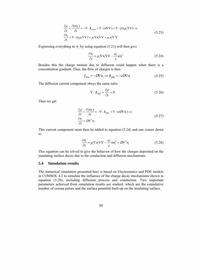
From the comparison of corona pulse number evolution at three applied voltage levels, as shown in Figures 5.10 through 5.12, the following can be observed:
When the applied voltage is just above the inception voltage, the cumulative corona pulse number evolution behavior has a good agreement with the situation of diffusion processes, as shown in Figure 5.10. The diffusion coefficient
4 2 -11 1.5 10 m sD is obtained in simulation 1, and the simulation 2 gives the
coefficients of 8 2 -1 9 2 -11 210 m s , 2 10 m sD D , which is more reasonable
compared with the values mentioned in [34], with the assumption that the diffusion process could happen not only on the surface but also into the bulk of the material.
The dominant mechanism of surface charge decay is the diffusion process along
0 0.02 0.04 0.06 0.08 0.10
100
200
300
400
500
600
700
800
Time [s]
Vp
[V]
Surface conductionBulk conduction
38
the surface as well as into the bulk of the insulating material at a lower applied voltage level.
The cumulative corona pulse number shows a linear behavior after 20 ms voltage applied at a higher voltage level, with the results as seen in Figure 4.8 (b), and the virgin curves all show the linear behavior from the beginning except the time delay after the voltage is applied. For example, the simulation in Figure 5.11 gives the value of mobility 11 2
1 2.775 10 m /(V s) .
This strong linear relation is mainly due to the surface conduction on the insulating surface; even though the diffusion and bulk conduction were included in the model, all of those mechanisms could not shift the main trend of this behavior.
Figure 5.10 The comparison of the cumulative corona pulse number behavior for the case of
4 kVV and 12 27.2 10 (C / (V s))K
0 0.02 0.04 0.06 0.08 0.10
50
100
150
200
250
300
350
400
450
500
550
Time [s]
Nto
t(t)
Simulation 1Simulation 2Measurement

39
Figure 5.11 The comparison of the total cumulative corona pulse behavior for the case of 4.8 kVV and 12 20.8 10 (C / (V s))K
Figure 5.12 The comparison of the cumulative corona pulse number behavior for the case of 5.4 kVV and 12 20.6 10 (C / (V s))K
0 0.02 0.04 0.06 0.08 0.10
100
200
300
400
500
600
700
800
900
Time [s]
Nto
t(t)
MeasurementSimulation
0 0.02 0.04 0.06 0.08 0.10
200
400
600
800
1000
1200
1400
1600
1800
2000
Time [s]
Nto
t(t)
MeasurementSimulation 1Simulation 2

40

41
Chapter 6
Summary of Papers
Paper I
In this paper, partial discharge measurements are performed in a narrow dielectric gap between spherical electrodes. The usual AC voltage sinusoidal waveform application is compared with a new method based on repetitive AC voltage pulses, with either alternating or unipolar polarity. The AC pulse with duration 1T is
followed by a zero voltage period of duration 2T . The work is limited to the case of 10 ms duration of AC pulse, i.e. 50 Hz-like, but a pause between every two AC pulses can be varied. The results show that the differences between the two methods and the influence of a pause between two half-sine voltage periods to the discharge behavior.
Paper II
In this paper, partial discharge tests are measured in the same setup as that in Paper I but with a perodic linear ramping voltage stimulus, which is a linear increasing voltage of fixed duration, combined with a linear decreasing voltage of variable duration. The effect of the different decreasing period on the discharge activity is investigated. The results show that an increasing fall time of the voltage gives rise to larger discharge pulses. The total charge per half-cycle grows with time as a power-law with exponent 1 2 , which indicates that a diffusion process of the deposited charge into the dielectric material may be responsible.
Paper III
In this paper, corona discharges are carried out in a needle-plane gap where the plane is covered by an insulating material. The discharge activity is measured during application of a periodic negative step voltage, whose duration of the voltage perio
1T and the pause time 2T between every two consecutive step voltage pulses could be varied separately to influence the decay of deposited surface charges. Compared with the discharge in the needle-plane setup without dielectric, the effect of a thin dielectric layer placed on the surface of the ground electrode on the corona activity is investigated. The results are shown for the case of the step voltage with duration of 100 ms and pause time of 10 s. Besides this, a simple RC model was created to
42
simulate the insulating material. The results show that the dielectric layer strongly affects the corona pulse number behavior, and corona discharge activity is dependent on the applied voltage level as well as the time of voltage applied.
Paper IV
This paper continues the work in Paper III. From the observation of corona discharge behavior in the situation of dielectric layer covering the surface of the ground electrode, a FEM based numerical model was developed to explain the measurement results from Paper III. The charge decay mechanisms on a corona charged dielectric surface are investigated based on a comparison between experiments and simulation results. The results show the dominant mechanism to charge decay processes in different applied voltage levels.

43
Chapter 7
Conclusions and Future Work
A novel off-line partial discharge diagnostic method is explored that is based on arbitrary waveform voltage stimulus. The main objective of the project is to investigate the decay process of surface charges deposited on the insulating material by the previous discharge activities, which could help us to understand the partial discharge behavior in a better way. The measurement results presented in this thesis are acquired by a time-resolved measurement system and analyzed by the pulse sequence analysis method. A FEM-based numerical model has been built to compare with the measurement results and get the deeper insight of corona discharge. From the results presented here, the following could be concluded:
For the case of applied alternating AC pulses, a tendency of increasing maximum pulse amplitude happens with increased pause time, an effect which may indicate that the cavity returns towards its virgin state between the half-sine pulses with less available seed electrons for the first discharge. It is also observed that there is seldom a discharge occurring during the pause period.
Unipolar positive half-sine pulses require a voltage almost double as for standard 50 Hz AC. Above inception the discharge behavior forms a pattern with positive discharges during rising voltage and negative during falling voltage.
An increasing fall time of the linearly ramped voltage gives rise to larger discharge pulses. The total charge per half-cycle grows with time as a power-law with exponent 1 2 , which indicates that a diffusion process of the deposited charge into the dielectric material may be responsible.
In the application of periodic negative step voltage, the PD activity during the first voltage cycle is significantly different from the others. For a lower voltage, the pulse repetition in the virgin curve reaches a saturation level within the charging period; however, for a higher voltage it increases more linearly.
From the comparison between the measurement and simulation results of corona discharge, one can indicate that the surface charge may decay by diffusion on the insulating surface and into the bulk of material when the applied voltage is a little higher than the inception voltage; however, with the increasing applied voltage, the main dominant mechanism of charge decay is surface conduction, which shows a linear behavior of the total number of discharge pulses with time.
44
For the next stage of this project, the following studies are of importance:
Based on the measurement results and numerical model in Paper IV, the continued work is required to investigate the effect of different material and the thickness of material on the evolution of corona pulse number. The model could be improved to be able to fit the measurement results better. Some other arbitrary voltage can be applied to have a better understanding of physical process of needle-plane corona discharge.
The partial discharge in the cavity needs to be further studied, based on Paper I and II. More measurements will be carried out in this well-defined situation. The charge decay processes of the charges deposited on the cavity wall will be investigated in conjunction with the numerical simulation.
The effect of the environment condition, such as temperature, and humidity on the discharge activities can also be investigated.
The partial discharge measurement with arbitrary voltage waveform stimulus can also be applied to stator bars.
45
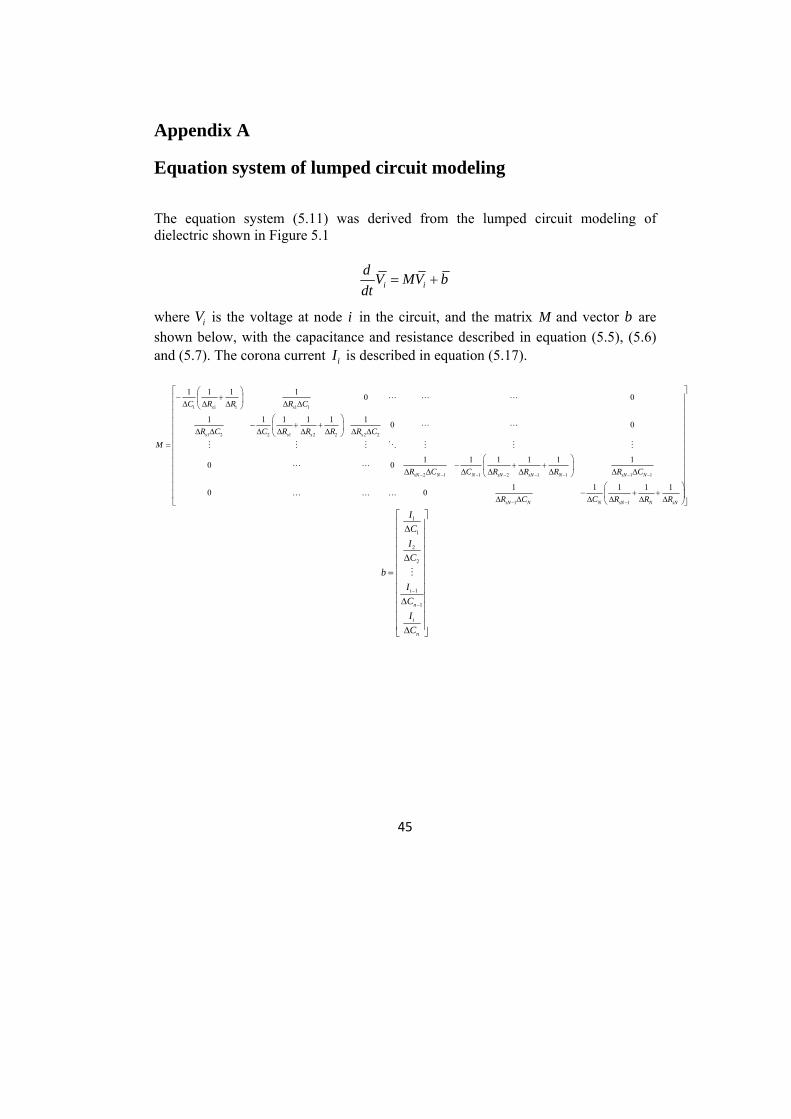
Appendix A
Equation system of lumped circuit modeling
The equation system (5.11) was derived from the lumped circuit modeling of dielectric shown in Figure 5.1
i i
dV MV b
dt
where iV is the voltage at node i in the circuit, and the matrix M and vector b are shown below, with the capacitance and resistance described in equation (5.5), (5.6) and (5.7). The corona current iI is described in equation (5.17).
1 1 1 1 1
1 2 2 1 2 2 2 2
2 1 1 2 1 1 1 1
1 1
1 1 1 1
1 1 1 1 1 1
1 1
0
1 1
0
0
1 1
1 1 1 1 1
0
0 0
0 0
s s
s s s s
sN N N sN sN N sN N
sN N N sN N sN
C R R R C
R C C R R R R C
R C C R R R R C
R C C R R
M
R
1
1
2
2
1
1
i
n
i
n
I
C
I
C
b
I
C
I
C

46
47
References
[1] A. Haddad, D. Warne, “Advances in High Voltage Engineering”, The Institution of Engineering and Technology, London, UK, 2004.
[2] H. Edin. Partial discharges studied with varible frequency of the applied voltage, PhD thesis, KTH, Stockholm, Sweden, 2001.
[3] C. Forssén. Modelling of cavity partial discharges at varible applied frequency, PhD thesis, KTH, Stockholm, Sweden, 2008.
[4] C. Forssén, H. Edin, “Partial discharges in a cavity at variable applied frequency part 1: measurements,” IEEE Transactions on Dielectrics and Electrical Insulation, Vol. 15, 1601-1609, 2008.
[5] C. Forssén, H. Edin, “Partial discharges in a cavity at variable applied frequency Part 2: measurements and modeling,” IEEE Transactions on Dielectrics and Electrical Insulation, 15, 1610-1616, 2008.
[6] F. J. Wester, E. Gulski, and J. J. Smith, “Detection of partial discharges at different AC voltage stresses in power cables,” IEEE Electr. Insul. Mag., 23(4), 28-43, 2007.
[7] M. Ghaffarian Niasar, H. Edin, X. Wang and R. Clemence, “Partial discharge characteristics due to air and water vapor bubbles in oil,” XVII International Symposium on High Voltage Engineering, Hannover, Germany, D-067, 2011.
[8] M. Farahani, H. Borsi, E. Gockenbach, M. Kaufhold, “Partial discharge and dissipation factor behavior of model insulating systems for high voltage rotating machines under different stresses”, IEEE Electrical Insulation Magazine, 21(5), 5-19, 2005.
[9] R. Patsch, F. Berton, “Pulse sequence analysis-a diagnostic tool based on the physics behind partial discharges,” J. Phys. D: Appl. Phys., 35, 25-32, 2002.
[10] M. Hoof, R. Patsch, “A physical model, describing the nature of partial discharge pulse sequences,” Int. Conf on Properties and Applications of Dielectric Materials, Seoul, Korea, 283-286, 1997.
[11] M. Hoof, R. Patsch, “Analyzing partial discharge pulse sequence-a new approach to investigate degradation phenomena,” IEEE International Symposium on Electrical Insulation, Pittsburgh, USA, 327-331, 1994.
[12] H. Kranz, “PD pulse sequence analysis and its relevance for on-site PD defect identification and evaluation,” IEEE Transactions on Dielectrics and Electrical Insulation, Vol. 12, 276-284, 2005.
[13] H. R. Mirzaei, A. Akbari, M. Aharezi, A. M. Jafari. “Experimental investigation of PD diagnosis based on consecutive pulses data,” Int. Conf on Condition Monitoring and Diagnosis, Beijing, China, 1262-1265, 2008.
[14] B. G. Stewart, L. Yang, M. D. Judd, A. Reid, and R. A. Fouracre, “A simple metric for assessing the severity of partial discharge activity based on time-
48
sequence-analysis-discharge level patterns,” Transactions on Electrical and Electronic Materials, Vol. 7, 313-318, 2006.
[15] A. Pfeffer, S. Tenbohlen, S. Kornhuber, “Pulse-sequence analysis of partial discharges in power transformers”, XVII International Symposium on High Voltage Engineering, Hannover, Germany, D-041, 2011.
[16] R. Brütsch, M. Tari, K Fröhlich, T Weiers, R Vogelsang, “Insulation failure machanisms of power generators”, IEEE Electrical Insulation Magazine, 24(4), 17-25, 2008.
[17] N. Taylor. Dielectric response and partial discharge measurements on stator insulation at varied low frequency, PhD thesis, KTH, Stockholm, Sweden, 2010.
[18] M. Goldman, R. S. Sigmond, “Corona and Insulation”, IEEE Transactions on Electrical Insulation., EI-17(2), 90-105, 1982.
[19] K. J. McLean, I. A. Ansari, “Calculation of the rod-plane voltage/current characteristics using the saturated current density equation and Warburg’s law”, IEE Proc., 134(10, Part A), 784-788, 1987.
[20] B. L. Henson, “Toward a fundamental model for steady point-plane corona discharges”, J. Appl. Phys., 55(1), 150-157, 1984.
[21] X. Meng, H. Zhang, and J. Zhu, “A general empirical formula of current-voltage characteristics for point-to-plane geometry corona discharges”, J. Phys. D: Appl. Phys., Vol. 41, 1-10, 2008.
[22] J. A. Cross, “Electrostatics: principles, problems and applications”, Adam Hilger, Bristol, UK, 1987.
[23] G. C. Montanari, “Bringing an insulation to failure: the role of space charge”, Int. Conf on Electrical Insulation and Dielectric Phenomena (CEIDP), West Lafayette, Indiana, USA, 1-25, 2010.
[24] J. Kindersberger, C. Lederle, “Surface charge decay on insulators in air and sulfurhexafluorid-Part I: Simulation”, IEEE Transactions on Dielectrics and Electrical Insulation., 15(4), 941-948, 2008.
[25] J. Kindersberger, C. Lederle, “Surface charge decay on insulators in air and sulfurhexafluorid-Part II: Measurements”, IEEE Transactions on Dielectrics and Electrical Insulation., 15(4), 949-957, 2008.
[26] P. Molinié, “Measuring and modeling transient insulator response to charging: the contribution of surface potential studies”, IEEE Transactions on Dielectrics and Electrical Insulation., 12(5), 939-950, 2005.
[27] D. M. Taylor, and T. P. T. Williams, “Decay of surface charge in the presence of a time-dependent bulk conductivity”, J. Phys. C: Solid State Phys., Vol. 11, 111-117, 1978.
[28] A. Crisci, “Surface-potential decay due to surface conduction”, Eur. Phys. J. AP, Vol. 4, 107-116, 1998.
[29] I. Somerville, and P. Vidaud, “Surface spreading of charge due to ohmic conduction”, Proc. R. Soc. Lond A, Vol. 399, 277-293, 1985.

49
[30] B. Lutz, and J. Kindersberger, “Determination of volume resistivity of polymeric insulators by surface charge decay”, Int. Symposium on High Voltage Engineering, Paper A-4, Johannesburg, 2009.
[31] S. Kumara, Y. V. Serdyuk, and S. M. Gubanski, “Surface charge decay on polymeric materials under different neutralization modes in air”, IEEE Trans. Dielectr. Electr. Insul., Vol. 18, No. 5, 1779-1788, 2008.
[32] H. J. Wintle, “Charge motion and trapping in insulators: surface and bulk effects”, IEEE Int. Symposium on Electrical Insulation, Arlington, Virginia, USA, 1-11, 1998.
[33] M. Campos, and J. A. Giacometti, “Surface potential decay in insulators with deep traps”, J. Appl. Phys., Vol. 52, No.7, 4546-4552, 1981.
[34] E. A. Baum, T. J. Lewis and R. Toomer, “The lateral motion of charge on thin films of polyethylene terephthalate,” J. Phys. D: Appl. Phys., 11, 963-977, 1978.
[35] P. ATorpey, “Double-carrier injection and recombination in insulators, including diffusion effects”, J. Appl. Phys., 56(8), 2284-2294, 1984.
[36] G. Teyssedre, C. Laurent, “Charge transport modeling in insulating polymers: from molecular to macroscopic scale”, IEEE Transactions on Dielectrics and Electrical Insulation., 12(5), 857-875, 2005.
[37] J. Liesegang, B. C. Senn, and E. R. Smith, “Resistivity of static and antistatic insulators from surface charge measurement”, J. Appl. Phys., Vol. 77, No. 11, 5782-5785, 1995.
[38] J. Liesegang, and B. C. Senn, “Resistivity, charge diffusion, and charge depth determinations on charged insulator surfaces”, J. Appl. Phys., Vol. 80, No. 11, 6336-6339, 1996.
[39] X. L. Wang, R. Clemence, and H. Edin, Partial discharge analysis of a narrow dielectric gap with repetitive half-sine pulses, Int. Conf. on Electrical Insulation and Dielectric Phenomena (CEIDP), West Lafayette, Indiana, USA, 481-484, 2010.
[40] X. Wang, R. Clemence and H. Edin, Partial discharge analysis of a narrow dielectric gap with repetitive linear ramping pulses, Proc. Nordic Insulation Symposium (Nord-IS 11), Tampere, Finland, 53-56, 2011.
[41] P. Llovera, P. Molinié, “New methodology for surface potential decay measurments: application to study charge injection dynamics on polypropylene films”, IEEE Transactions on Dielectrics and Electrical Insulation., 11(6), 1049-1056, 2004.
[42] S. Sahli, A. Bellel, Z. Ziari, A. Kahlouche, Y. Segui, “Measure and analysis of potential decay in polypropylene films after negative corona charge deposition”, J. Electrostatics, 57, 169-191, 2003.
[43] G. Chen, “A new model for surface potential decay of corona-charged polymers”, J. Phys. D: Appl. Phys., 43, 1-7, 2010.
50
[44] E. A. Baum, T. J. Lewis and R. Toomer, “Decay of electrical charge on polyethylene films,” J. Phys. D: Appl. Phys., 10, 487-497, 1977.
[45] J. N. Chubb, “Corona charging of practical materials for charge decay measurements”, J. Electrostatics, 37, 53-65, 1996.
[46] A. Neves, H. J. A. Martins, “Surface charging and charge decay in solid dielectrics”, Conference Record of the 1996 IEEE International Symposium on Electrical Insulation, Montreal, Quebec, Canada, 782-786, 1996.
[47] R. Kacprzyk, “Influence of discharge conditions on the charge decay characteristics”, J. Electrostatics, 68, 190-195, 2010.
[48] B. Lutz, J. Kindersberger, “Influence of relative humidity on surface charge decay on epoxy resin insulators”, Proceedings of the 9th International Conference on Properties and Applications of Dielectric Materials, 883-886, Harbin, China, 2009.
[49] T. Jing, P. H. F. Morshuis, F. H. Kreuger, “Surface charge accumulation and decay on a spacer stressed with DC voltages at atmospheric conditions”, Archiv für Elektrotechnik, 74, 315-319, 1991.
[50] P. Molinié, M Goldman, J Gatellet, “Surface potential decay on corona-charged epoxy samples due to polarization processes”, J. Phys. D: Appl. Phys., 28, 1601-1610, 1995.
[51] P. Molinié, “Charge injection in corona-charged polymeric films: potential decay and current measurements” J. Electrostatics, 45, 265-273, 1999.
[52] H. J. Wintle, M. P. Pépin, “Decay of surface charge between electrodes on insulator surfaces”, J. Electrostatics, 48, 115-126, 2000.
[53] P. A. Heimann, J. E. Olsen, “A sensitive method for measuring surface conductivity of insulators”, J. Appl. Phys., 53(1), 546-549, 1983.
[54] I. W. McAllister, “Decay of charge deposited on the wall of a gaseous void”, IEEE Transactions on Electrical Insulation., 27(6), 1202-1207, 1992.
[55] D. K. Das-Gupta, “Surface charge decay on insulating films”, Conference Record of the 1988 IEEE International Symposium on Electrical Insulation, Boston, MA, USA, 296-299, 1988.
[56] A. Kumada, S. Okabe, “Charge distribution measurement on a truncated cone spacer under dc voltage”, IEEE Transactions on Dielectrics and Electrical Insulation., 11(6), 929-938, 2004.
[57] K. Kato, S. Kaneko, S. Okabe, H. Okubo, “Numerical calculation model for electric field distribution in gas/solid composite insulation system under dc voltage application”, Proceeding of International Symposium on Eco Topia Science (ISETS07), 514-515, 2007.