Partial Discharge Measurement under an Oscillating ...
14
energies Article Partial Discharge Measurement under an Oscillating Switching Impulse: A Potential Supplement to the Conventional Insulation Examination in the Field Ming Ren *, Ming Dong *, Chongxing Zhang and Jierui Zhou State Key Laboratory of Electrical Insulation for Power Equipment, Xi’an Jiaotong University, Xi’an 710049, China; [email protected] (C.Z.); [email protected] (J.Z.) * Correspondence: [email protected] (M.R.); [email protected] (M.D.) Academic Editor: Paul Stewart Received: 14 June 2016; Accepted: 1 August 2016; Published: 9 August 2016 Abstract: Partial discharge (PD) detection under oscillating switching impulse (OSI) voltage was performed on three types of insulation defects, including a protrusion on a conductor, a particle on an insulator surface, and a void in an insulator, which are three kinds of the common potential insulation hazards in gas insulated power apparatus. Experiment indicated that the PD sequences under OSI were composed of various combinations of the single pulse, the multiple pulses, and the reverse polarity pulse. The difference between the PD inception voltage (PDIV) and the breakdown voltage (BDV) under OSI voltage was greater than that under alternating current (AC) voltage in some cases, which can provide a more sufficient margin below the BDV for PD diagnosis. The OSI voltage also showed a better performance for exciting PDs with detectable magnitudes from small-scale defects, of which the AC voltage was incapable under our test conditions. The different PD activities with different interfaces under an impulse and a slowly varying voltage were speculated to be associated with the gradient of the background electric field and the space-charge mobility. Keywords: gas insulated switchgear; power apparatus; partial discharge; impulse voltage; SF 6 ; insulation diagnosis 1. Introduction Partial discharge (PD) detection has been widely used in the quality control of high-voltage power apparatus serving a power system, by which the overall insulation status and local condition are expected to be examined during routine tests, handing over tests and even field tests. An AC withstand test combined with PD detection has become a compulsory test during delivery, especially for an ultrahigh-voltage gas-insulated switchgear or a transmission line. The insulation defects are caused by manufacturing errors at the factory as well as transportation and assembly in the field. Thus, a short-time AC resonant withstand test needs to be implemented after assembly and repair, and a PD test is also applied in an effort to determine any unknown damage. Aside from these tests, some online diagnostic techniques, particularly the ultrahigh frequency (UHF) method and acoustical wave (AE) method [1], have been developed to avoid insulation failure during operation. Admittedly, these offline and online methods have served irreplaceable roles in insulation diagnosis for many years. However, practical experience and studies have shown that the AC PD test is probably not a universal solution for finding all types of insulation defects, especially for conductive protrusions and particles on the insulator surface. This problem is supposed to be subject to diffusion-limited charge accumulation, which confines the discharge intensity to an undetectable level [2,3]. Some hidden defects are hardly exposed by the AC voltage field test and can continuously deteriorate the insulation and shorten the service life of the equipment prior to failure. An increasing number of failures have occurred Energies 2016, 9, 623; doi:10.3390/en9080623 www.mdpi.com/journal/energies
Transcript of Partial Discharge Measurement under an Oscillating ...

energies
Article
Partial Discharge Measurement under an OscillatingSwitching Impulse: A Potential Supplement to theConventional Insulation Examination in the FieldMing Ren *, Ming Dong *, Chongxing Zhang and Jierui Zhou
State Key Laboratory of Electrical Insulation for Power Equipment, Xi’an Jiaotong University,Xi’an 710049, China; [email protected] (C.Z.); [email protected] (J.Z.)* Correspondence: [email protected] (M.R.); [email protected] (M.D.)
Academic Editor: Paul StewartReceived: 14 June 2016; Accepted: 1 August 2016; Published: 9 August 2016
Abstract: Partial discharge (PD) detection under oscillating switching impulse (OSI) voltage wasperformed on three types of insulation defects, including a protrusion on a conductor, a particleon an insulator surface, and a void in an insulator, which are three kinds of the common potentialinsulation hazards in gas insulated power apparatus. Experiment indicated that the PD sequencesunder OSI were composed of various combinations of the single pulse, the multiple pulses, and thereverse polarity pulse. The difference between the PD inception voltage (PDIV) and the breakdownvoltage (BDV) under OSI voltage was greater than that under alternating current (AC) voltage in somecases, which can provide a more sufficient margin below the BDV for PD diagnosis. The OSI voltagealso showed a better performance for exciting PDs with detectable magnitudes from small-scaledefects, of which the AC voltage was incapable under our test conditions. The different PD activitieswith different interfaces under an impulse and a slowly varying voltage were speculated to beassociated with the gradient of the background electric field and the space-charge mobility.
Keywords: gas insulated switchgear; power apparatus; partial discharge; impulse voltage; SF6;insulation diagnosis
1. Introduction
Partial discharge (PD) detection has been widely used in the quality control of high-voltagepower apparatus serving a power system, by which the overall insulation status and local conditionare expected to be examined during routine tests, handing over tests and even field tests. An ACwithstand test combined with PD detection has become a compulsory test during delivery, especiallyfor an ultrahigh-voltage gas-insulated switchgear or a transmission line. The insulation defects arecaused by manufacturing errors at the factory as well as transportation and assembly in the field. Thus,a short-time AC resonant withstand test needs to be implemented after assembly and repair, and a PDtest is also applied in an effort to determine any unknown damage. Aside from these tests, some onlinediagnostic techniques, particularly the ultrahigh frequency (UHF) method and acoustical wave (AE)method [1], have been developed to avoid insulation failure during operation. Admittedly, these offlineand online methods have served irreplaceable roles in insulation diagnosis for many years. However,practical experience and studies have shown that the AC PD test is probably not a universal solutionfor finding all types of insulation defects, especially for conductive protrusions and particles on theinsulator surface. This problem is supposed to be subject to diffusion-limited charge accumulation,which confines the discharge intensity to an undetectable level [2,3]. Some hidden defects are hardlyexposed by the AC voltage field test and can continuously deteriorate the insulation and shortenthe service life of the equipment prior to failure. An increasing number of failures have occurred
Energies 2016, 9, 623; doi:10.3390/en9080623 www.mdpi.com/journal/energies
Energies 2016, 9, 623 2 of 14
prior to the end of the designed service life. In this case, the impulse voltage test is expected to be aneffective supplement to an insulation quality examination in the field because of its high-field effectand limited destructiveness. To address the inconvenience due to the low delivery efficiency of theimpulse generator, the IEC 60060-3 standard recommends oscillating impulse voltages as alternativesto aperiodic impulses, which are more feasible in a field test [4]. Figure 1 shows an ongoing oscillatingimpulse withstand test of a gas-insulated switchgear in the field.
Energies 2016, 9, 623 2 of 14
test is expected to be an effective supplement to an insulation quality examination in the field because
of its high-field effect and limited destructiveness. To address the inconvenience due to the low
delivery efficiency of the impulse generator, the IEC 60060-3 standard recommends oscillating
impulse voltages as alternatives to aperiodic impulses, which are more feasible in a field test [4].
Figure 1 shows an ongoing oscillating impulse withstand test of a gas-insulated switchgear in the field.
Figure 1. On-going oscillating impulse withstand test implemented on gas insulated switchgear in
the field.
Thus, PD detection could be simultaneously performed with withstand tests to exclude the
critical defects arising from transportation and assembly [5]. In the past few decades, the gap
breakdown in stressed SF6 gas under impulse conditions has been extensively studied [6–8]. Relevant
theories based on the streamer and leader mechanisms have been developed by experiments [9] and
simulations [10,11]. The aims of most of these previous studies were the design of the power
equipment and the failure mechanisms of the SF6 insulation. The PDs under impulse conditions were
generally thought to be phenomena occurring in the initial stage of breakdown and seldom studied
in terms of insulation diagnosis. Further, we have previously investigated the PD characteristics and
impact factors under lightning and switching impulses for various artificial defects in SF6 gas [12,13].
On the basis of previous studies, this paper summarizes the PDs under impulse voltages from
the viewpoint of insulation diagnosis in practice. The PD behaviors under an oscillating switching
impulse (OSI) are described by exemplifying the typical PD sequences and PD pulses caused by
different defects. The effectiveness of various voltages including the switching impulse (SI),
oscillating switching impulse (OSI), and AC voltages on the PD diagnosis is quantitatively compared.
The reasons for the different PD activities under an impulse and a slowly varying voltage are
discussed, and they are speculated to be associated with the field-dependent stabilization effect.
2. Experimental Setup
2.1. Partial Discharge (PD) Measurement under Impulse Conditions
Under surge voltage conditions, one difficult problem in PD detection is the separation of PD
signals with a magnitude on the order of approximately a few milliamperes from the great capacitive
displacement flow on the order of approximately a few amperes. For example, a 65 kV oscillating
Figure 1. On-going oscillating impulse withstand test implemented on gas insulated switchgear inthe field.
Thus, PD detection could be simultaneously performed with withstand tests to exclude the criticaldefects arising from transportation and assembly [5]. In the past few decades, the gap breakdown instressed SF6 gas under impulse conditions has been extensively studied [6–8]. Relevant theories based onthe streamer and leader mechanisms have been developed by experiments [9] and simulations [10,11].The aims of most of these previous studies were the design of the power equipment and the failuremechanisms of the SF6 insulation. The PDs under impulse conditions were generally thought to bephenomena occurring in the initial stage of breakdown and seldom studied in terms of insulationdiagnosis. Further, we have previously investigated the PD characteristics and impact factors underlightning and switching impulses for various artificial defects in SF6 gas [12,13].
On the basis of previous studies, this paper summarizes the PDs under impulse voltages fromthe viewpoint of insulation diagnosis in practice. The PD behaviors under an oscillating switchingimpulse (OSI) are described by exemplifying the typical PD sequences and PD pulses caused bydifferent defects. The effectiveness of various voltages including the switching impulse (SI), oscillatingswitching impulse (OSI), and AC voltages on the PD diagnosis is quantitatively compared. The reasonsfor the different PD activities under an impulse and a slowly varying voltage are discussed, and theyare speculated to be associated with the field-dependent stabilization effect.
2. Experimental Setup
2.1. Partial Discharge (PD) Measurement under Impulse Conditions
Under surge voltage conditions, one difficult problem in PD detection is the separation of PDsignals with a magnitude on the order of approximately a few milliamperes from the great capacitive

Energies 2016, 9, 623 3 of 14
displacement flow on the order of approximately a few amperes. For example, a 65 kV oscillatinglightning impulse (OLI) voltage applied to a test object with a capacitance of 75 pF could producea displacement current above 2 A, as shown in Figure 2.
Energies 2016, 9, 623 3 of 14
lightning impulse (OLI) voltage applied to a test object with a capacitance of 75 pF could produce a
displacement current above 2 A, as shown in Figure 2.
Figure 2. PD signals superimposed on the current flow under an impulse.
To address this problem, a capacitor could be employed as the balance bridge in parallel with
the test object [14]. This method is effective for the capacitive specimen under an AC voltage but
unsatisfactory under impulse conditions because the equivalent circuit is no longer a
lumped-parameter circuit but distributed. Moreover, it is also difficult to obtain the equivalent
parameters for each specific condition, especially in a field test. Another approach is to filter the surge
flow that occupies the relatively low frequency range by introducing a second-order RC filtering
circuit at the front of the preamplifier, as shown in Figure 3. However, this approach gives rise to a
serious decrease in the sensitivity for PD detection due to the large ratio of the surge amplitude in
the low-frequency range to the PD magnitude at a high frequency. In this study, a feasible PD
detection circuit was applied under impulse conditions, as shown in Figure 3. Signal coupling is
realized by two current transformers (CTs), both of which were placed around the ground pillars.
One wideband CT (CT1, 20 kHz–110 MHz, 5 V/A, IPC-CM-500) responds to the total transient signal
over a wide frequency range covering the displacement-current and PD signals. CT2 was a
homemade CT (3 kHz–1.7 MHz, 5 V/A), which only responds to the displacement-current signal in
the low-frequency range. By subtracting the output of CT2 from that of CT1 with a differential
amplifier, most of the displacement component in the total current signal could be canceled. Finally,
the output of the differential module was processed by a high-pass filter to separate the PDs from the
residual displacement current. A CT could be employed for impulse PD detection because it can
quantify the severity of the PD and can be conveniently installed on power equipment without
contact. The sensitivities of the measurement systems for the impulse PD and AC PD can be verified
by calibration, and their minimum detectable levels are 5 pC and 2.0 pC, respectively. The simplified
circuit of the oscillating impulse generator used in the experiment is shown in the dotted box in
Figure 4, by which OSI voltage (33/1000 μs, 8 kHz) can be produced. The waveform of the OSI voltage
is shown in Figure 5.
Figure 2. PD signals superimposed on the current flow under an impulse.
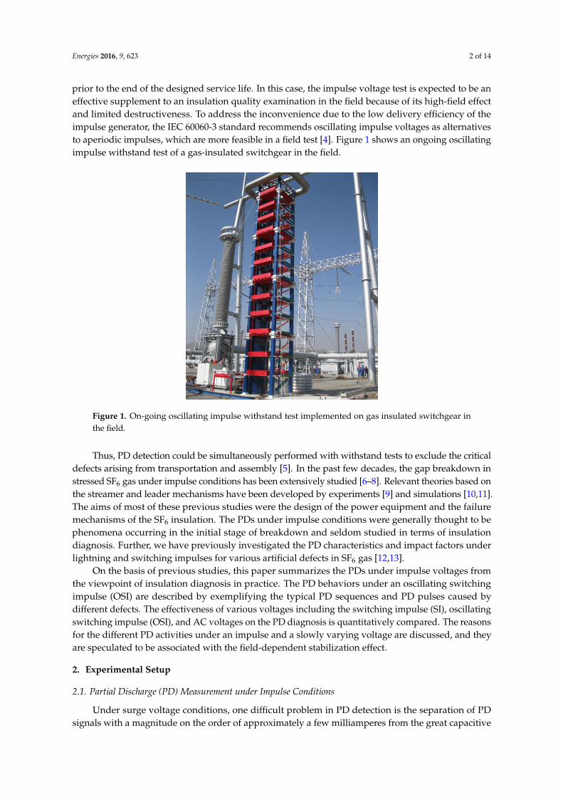
To address this problem, a capacitor could be employed as the balance bridge in parallel with the testobject [14]. This method is effective for the capacitive specimen under an AC voltage but unsatisfactoryunder impulse conditions because the equivalent circuit is no longer a lumped-parameter circuit butdistributed. Moreover, it is also difficult to obtain the equivalent parameters for each specific condition,especially in a field test. Another approach is to filter the surge flow that occupies the relatively lowfrequency range by introducing a second-order RC filtering circuit at the front of the preamplifier, asshown in Figure 3. However, this approach gives rise to a serious decrease in the sensitivity for PDdetection due to the large ratio of the surge amplitude in the low-frequency range to the PD magnitudeat a high frequency. In this study, a feasible PD detection circuit was applied under impulse conditions,as shown in Figure 3. Signal coupling is realized by two current transformers (CTs), both of which wereplaced around the ground pillars. One wideband CT (CT1, 20 kHz–110 MHz, 5 V/A, IPC-CM-500)responds to the total transient signal over a wide frequency range covering the displacement-currentand PD signals. CT2 was a homemade CT (3 kHz–1.7 MHz, 5 V/A), which only responds to thedisplacement-current signal in the low-frequency range. By subtracting the output of CT2 from thatof CT1 with a differential amplifier, most of the displacement component in the total current signalcould be canceled. Finally, the output of the differential module was processed by a high-pass filter toseparate the PDs from the residual displacement current. A CT could be employed for impulse PDdetection because it can quantify the severity of the PD and can be conveniently installed on powerequipment without contact. The sensitivities of the measurement systems for the impulse PD and ACPD can be verified by calibration, and their minimum detectable levels are 5 pC and 2.0 pC, respectively.The simplified circuit of the oscillating impulse generator used in the experiment is shown in thedotted box in Figure 4, by which OSI voltage (33/1000 µs, 8 kHz) can be produced. The waveform ofthe OSI voltage is shown in Figure 5.
Energies 2016, 9, 623 4 of 14
Energies 2016, 9, 623 4 of 14
Figure 3. A preposing signal process circuit for PD measurement. The loop consisting of C1, C2, C3,
R1, and R2 is employed as a second-order RC filter. R3 and R4 are used for gain control.
Figure 4. Measurement circuits for impulse PD detection. Rs: the current-limiting resistor, 1 MΩ; C0:
the test sample, 60–160 pF; Cp: the coupling capacitor for PD detection, 1.6 nF; C1: the DC charging
capacitor, 0.0111 µF; Rf: the wave-front-adjusting resistor, 3.0 kΩ; Rt: the wave-tail-adjusting resistor,
300 kΩ; Lf: the adjusting inductor, 85.3 mH.
Figure 5. The waveform of the OSI voltage. T1: front time; T2: time-to-half-value; f: oscillating frequency.
2.2. Artificial Defect Models and Experimental Setup
In our experiment, a stainless-steel test chamber that could withstand a gas pressure up to
0.7 MPa and applied voltages up to 150 kV (50 Hz AC peak) was used to build a SF6 gas insulated
system, as shown in Figure 6a. Any specific insulation system may contain some insulation defects,
which arise from the design, manufacturing, assembling, and service stress history. According to the
nature of the two or three major dielectric boundaries, the insulation defects could be classified and
simplified into small-scale defect models which can be used in experimental studies. Considering the
contribution of the electric field to the excitation of the PDs, three defect models including a metal
protrusion (see Figure 6b), a metal particle (a metal needle was employed as the particle) on an
insulator surface (see Figure 6c), and a gaseous void in an insulator (see Figure 6d) were developed
to simulate the defects with different dielectric interfaces. In our test, all the defect models were
placed in a pair of parallel plate copper electrodes which can provide a uniform background electric
field. The protrusion defects (as shown in Figure 6b,c) were made of stainless steel (Crl8Ni9Ti). To
make the void defect model (see Figure 6d), two epoxy resin plates, each with an artificial pitting at
the center, were spliced face to face by using a mixture of E51 epoxy resin (Deyuan Epoxy Resin Co.,
Figure 3. A preposing signal process circuit for PD measurement. The loop consisting of C1, C2, C3,R1, and R2 is employed as a second-order RC filter. R3 and R4 are used for gain control.
Energies 2016, 9, 623 4 of 14
Figure 3. A preposing signal process circuit for PD measurement. The loop consisting of C1, C2, C3,
R1, and R2 is employed as a second-order RC filter. R3 and R4 are used for gain control.
Figure 4. Measurement circuits for impulse PD detection. Rs: the current-limiting resistor, 1 MΩ; C0:
the test sample, 60–160 pF; Cp: the coupling capacitor for PD detection, 1.6 nF; C1: the DC charging
capacitor, 0.0111 µF; Rf: the wave-front-adjusting resistor, 3.0 kΩ; Rt: the wave-tail-adjusting resistor,
300 kΩ; Lf: the adjusting inductor, 85.3 mH.
Figure 5. The waveform of the OSI voltage. T1: front time; T2: time-to-half-value; f: oscillating frequency.
2.2. Artificial Defect Models and Experimental Setup
In our experiment, a stainless-steel test chamber that could withstand a gas pressure up to
0.7 MPa and applied voltages up to 150 kV (50 Hz AC peak) was used to build a SF6 gas insulated
system, as shown in Figure 6a. Any specific insulation system may contain some insulation defects,
which arise from the design, manufacturing, assembling, and service stress history. According to the
nature of the two or three major dielectric boundaries, the insulation defects could be classified and
simplified into small-scale defect models which can be used in experimental studies. Considering the
contribution of the electric field to the excitation of the PDs, three defect models including a metal
protrusion (see Figure 6b), a metal particle (a metal needle was employed as the particle) on an
insulator surface (see Figure 6c), and a gaseous void in an insulator (see Figure 6d) were developed
to simulate the defects with different dielectric interfaces. In our test, all the defect models were
placed in a pair of parallel plate copper electrodes which can provide a uniform background electric
field. The protrusion defects (as shown in Figure 6b,c) were made of stainless steel (Crl8Ni9Ti). To
make the void defect model (see Figure 6d), two epoxy resin plates, each with an artificial pitting at
the center, were spliced face to face by using a mixture of E51 epoxy resin (Deyuan Epoxy Resin Co.,
Figure 4. Measurement circuits for impulse PD detection. Rs: the current-limiting resistor, 1 MΩ;C0: the test sample, 60–160 pF; Cp: the coupling capacitor for PD detection, 1.6 nF; C1: the DC chargingcapacitor, 0.0111 µF; Rf: the wave-front-adjusting resistor, 3.0 kΩ; Rt: the wave-tail-adjusting resistor,300 kΩ; Lf: the adjusting inductor, 85.3 mH.
Energies 2016, 9, 623 4 of 14
Figure 3. A preposing signal process circuit for PD measurement. The loop consisting of C1, C2, C3,
R1, and R2 is employed as a second-order RC filter. R3 and R4 are used for gain control.
Figure 4. Measurement circuits for impulse PD detection. Rs: the current-limiting resistor, 1 MΩ; C0:
the test sample, 60–160 pF; Cp: the coupling capacitor for PD detection, 1.6 nF; C1: the DC charging
capacitor, 0.0111 µF; Rf: the wave-front-adjusting resistor, 3.0 kΩ; Rt: the wave-tail-adjusting resistor,
300 kΩ; Lf: the adjusting inductor, 85.3 mH.
Figure 5. The waveform of the OSI voltage. T1: front time; T2: time-to-half-value; f: oscillating frequency.
2.2. Artificial Defect Models and Experimental Setup
In our experiment, a stainless-steel test chamber that could withstand a gas pressure up to
0.7 MPa and applied voltages up to 150 kV (50 Hz AC peak) was used to build a SF6 gas insulated
system, as shown in Figure 6a. Any specific insulation system may contain some insulation defects,
which arise from the design, manufacturing, assembling, and service stress history. According to the
nature of the two or three major dielectric boundaries, the insulation defects could be classified and
simplified into small-scale defect models which can be used in experimental studies. Considering the
contribution of the electric field to the excitation of the PDs, three defect models including a metal
protrusion (see Figure 6b), a metal particle (a metal needle was employed as the particle) on an
insulator surface (see Figure 6c), and a gaseous void in an insulator (see Figure 6d) were developed
to simulate the defects with different dielectric interfaces. In our test, all the defect models were
placed in a pair of parallel plate copper electrodes which can provide a uniform background electric
field. The protrusion defects (as shown in Figure 6b,c) were made of stainless steel (Crl8Ni9Ti). To
make the void defect model (see Figure 6d), two epoxy resin plates, each with an artificial pitting at
the center, were spliced face to face by using a mixture of E51 epoxy resin (Deyuan Epoxy Resin Co.,
Figure 5. The waveform of the OSI voltage. T1: front time; T2: time-to-half-value; f : oscillating frequency.
2.2. Artificial Defect Models and Experimental Setup
In our experiment, a stainless-steel test chamber that could withstand a gas pressure up to 0.7 MPaand applied voltages up to 150 kV (50 Hz AC peak) was used to build a SF6 gas insulated system, asshown in Figure 6a. Any specific insulation system may contain some insulation defects, which arisefrom the design, manufacturing, assembling, and service stress history. According to the nature of thetwo or three major dielectric boundaries, the insulation defects could be classified and simplified intosmall-scale defect models which can be used in experimental studies. Considering the contributionof the electric field to the excitation of the PDs, three defect models including a metal protrusion(see Figure 6b), a metal particle (a metal needle was employed as the particle) on an insulator surface(see Figure 6c), and a gaseous void in an insulator (see Figure 6d) were developed to simulate thedefects with different dielectric interfaces. In our test, all the defect models were placed in a pair ofparallel plate copper electrodes which can provide a uniform background electric field. The protrusiondefects (as shown in Figure 6b,c) were made of stainless steel (Crl8Ni9Ti). To make the void defect

Energies 2016, 9, 623 5 of 14
model (see Figure 6d), two epoxy resin plates, each with an artificial pitting at the center, were splicedface to face by using a mixture of E51 epoxy resin (Deyuan Epoxy Resin Co., Ltd., Feicheng, China)and 10% DDS curing agent (Jianxin Imp & Exp Co., Ltd., Cangzhou, China). To ensure a good contactbetween the electrode and the epoxy resin without gas gap, the electrode was also spliced to the epoxyresin plate which has a void inside. After splicing, the defect samples were kept in a vacuum oven at55 ˝C for over 24 h for drying. The relative dielectric constant of the E51 and DDS mixture was 4.1–4.3,which is consistent with that of the epoxy resin block. The scale of the artificial defect was controlledby the parameters listed in Table 1.
Energies 2016, 9, 623 5 of 14
Ltd., Feicheng, China) and 10% DDS curing agent (Jianxin Imp & Exp Co., Ltd., Cangzhou, China).
To ensure a good contact between the electrode and the epoxy resin without gas gap, the electrode
was also spliced to the epoxy resin plate which has a void inside. After splicing, the defect samples
were kept in a vacuum oven at 55 °C for over 24 h for drying. The relative dielectric constant of the
E51 and DDS mixture was 4.1–4.3, which is consistent with that of the epoxy resin block. The scale of
the artificial defect was controlled by the parameters listed in Table 1.
Figure 6. SF6 test chamber and PD defect models. (a) Test chamber with PD sensors; (b) Metal
protrusion; (c) Metal particle on insulator surface; (d) Gaseous void in insulator. The plate electrodes
are made of copper, and the protrusion and needle are made of steel. D is the gap distance between
the plate electrodes. θ is the inclination angle of the insulator. L is the length of the protrusion or the
needle on the surface. a and b are the radius and the height of the gaseous void in the insulator,
respectively. The permittivity of epoxy is 4.1.
Table 1. Scale parameters of the three defects investigated.
Defects Gap Between the Plate Electrodes
(Background Field)
Defect Scale Parameters
(Locally Enhanced Field)
Protrusion D = 30 mm r = 0.7 mm, L = 1, 2, 5 10 mm
Surface particle D = 35 mm, θ = 60° r = 0.7 mm, L = 1, 2, 5, 10 mm
Void D = 20 mm x=a/b = 0.5, 2
V=πa2b = 2, 15, 45, 340 mm3
The overall configuration of the PD detection system is shown in Figure 7. The PD signals are
recorded by a digital oscilloscope (DSO, LeCroy 64Xs-B, Teledyne LeCroy, Chestnut Ridge, NY,
USA), sampling rate 10 Gs/s; analog bandwidth 600 MHz). To avoid electromagnetic (EM)
interference, metal armored double-shielded measurement cables were used for signal transmission.
All recording apparatus were placed in an EM-shielded room. The voltage divider used in the test
had a response time less than 100ns and a measurement range up to 150 kV. The coupling capacitance
value in parallel with the test object was 1000 pF. A photomultiplier tube (PMT, R7600U, Hamamatsu,
Japan), response over a wavelength range of 300–850 nm) for optical detection was placed behind the
observation window of the chamber and employed to assist with the PD current measurement. The
optical windows of the chamber were constructed of synthetic fused silica glass (above 85%
transmittance from 175 nm onward and 90% from 220 nm onward).
Figure 6. SF6 test chamber and PD defect models. (a) Test chamber with PD sensors; (b) Metalprotrusion; (c) Metal particle on insulator surface; (d) Gaseous void in insulator. The plate electrodesare made of copper, and the protrusion and needle are made of steel. D is the gap distance between theplate electrodes. θ is the inclination angle of the insulator. L is the length of the protrusion or the needleon the surface. a and b are the radius and the height of the gaseous void in the insulator, respectively.The permittivity of epoxy is 4.1.
Table 1. Scale parameters of the three defects investigated.
Defects Gap Between the Plate Electrodes(Background Field)
Defect Scale Parameters(Locally Enhanced Field)
Protrusion D = 30 mm r = 0.7 mm, L = 1, 2, 5 10 mmSurface particle D = 35 mm, θ = 60˝ r = 0.7 mm, L = 1, 2, 5, 10 mm
Void D = 20 mm x=a/b = 0.5, 2V=πa2b = 2, 15, 45, 340 mm3
The overall configuration of the PD detection system is shown in Figure 7. The PD signals arerecorded by a digital oscilloscope (DSO, LeCroy 64Xs-B, Teledyne LeCroy, Chestnut Ridge, NY, USA),sampling rate 10 Gs/s; analog bandwidth 600 MHz). To avoid electromagnetic (EM) interference,metal armored double-shielded measurement cables were used for signal transmission. All recordingapparatus were placed in an EM-shielded room. The voltage divider used in the test had a responsetime less than 100ns and a measurement range up to 150 kV. The coupling capacitance value in parallelwith the test object was 1000 pF. A photomultiplier tube (PMT, R7600U, Hamamatsu, Japan), responseover a wavelength range of 300–850 nm) for optical detection was placed behind the observationwindow of the chamber and employed to assist with the PD current measurement. The opticalwindows of the chamber were constructed of synthetic fused silica glass (above 85% transmittancefrom 175 nm onward and 90% from 220 nm onward).
Energies 2016, 9, 623 6 of 14Energies 2016, 9, 623 6 of 14
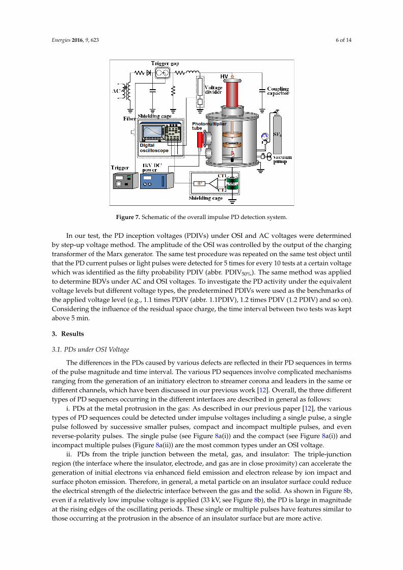
Figure 7. Schematic of the overall impulse PD detection system.
In our test, the PD inception voltages (PDIVs) under OSI and AC voltages were determined by
step-up voltage method. The amplitude of the OSI was controlled by the output of the charging
transformer of the Marx generator. The same test procedure was repeated on the same test object
until that the PD current pulses or light pulses were detected for 5 times for every 10 tests at a certain
voltage which was identified as the fifty probability PDIV (abbr. PDIV50%). The same method was
applied to determine BDVs under AC and OSI voltages. To investigate the PD activity under the
equivalent voltage levels but different voltage types, the predetermined PDIVs were used as the
benchmarks of the applied voltage level (e.g., 1.1 times PDIV (abbr. 1.1PDIV), 1.2 times PDIV
(1.2 PDIV) and so on). Considering the influence of the residual space charge, the time interval
between two tests was kept above 5 min.
3. Results
3.1. PDs under OSI Voltage
The differences in the PDs caused by various defects are reflected in their PD sequences in terms
of the pulse magnitude and time interval. The various PD sequences involve complicated
mechanisms ranging from the generation of an initiatory electron to streamer corona and leaders in
the same or different channels, which have been discussed in our previous work [12]. Overall, the
three different types of PD sequences occurring in the different interfaces are described in general
as follows:
i. PDs at the metal protrusion in the gas: As described in our previous paper [12], the various
types of PD sequences could be detected under impulse voltages including a single pulse, a single
pulse followed by successive smaller pulses, compact and incompact multiple pulses, and even
reverse-polarity pulses. The single pulse (see Figure 8a(i)) and the compact (see Figure 8a(i)) and
incompact multiple pulses (Figure 8a(ii)) are the most common types under an OSI voltage.
ii. PDs from the triple junction between the metal, gas, and insulator: The triple-junction region
(the interface where the insulator, electrode, and gas are in close proximity) can accelerate the
generation of initial electrons via enhanced field emission and electron release by ion impact and
surface photon emission. Therefore, in general, a metal particle on an insulator surface could reduce
the electrical strength of the dielectric interface between the gas and the solid. As shown in Figure 8b,
even if a relatively low impulse voltage is applied (33 kV, see Figure 8b), the PD is large in magnitude
at the rising edges of the oscillating periods. These single or multiple pulses have features similar to
those occurring at the protrusion in the absence of an insulator surface but are more active.
Figure 7. Schematic of the overall impulse PD detection system.
In our test, the PD inception voltages (PDIVs) under OSI and AC voltages were determinedby step-up voltage method. The amplitude of the OSI was controlled by the output of the chargingtransformer of the Marx generator. The same test procedure was repeated on the same test object untilthat the PD current pulses or light pulses were detected for 5 times for every 10 tests at a certain voltagewhich was identified as the fifty probability PDIV (abbr. PDIV50%). The same method was appliedto determine BDVs under AC and OSI voltages. To investigate the PD activity under the equivalentvoltage levels but different voltage types, the predetermined PDIVs were used as the benchmarks ofthe applied voltage level (e.g., 1.1 times PDIV (abbr. 1.1PDIV), 1.2 times PDIV (1.2 PDIV) and so on).Considering the influence of the residual space charge, the time interval between two tests was keptabove 5 min.
3. Results
3.1. PDs under OSI Voltage
The differences in the PDs caused by various defects are reflected in their PD sequences in termsof the pulse magnitude and time interval. The various PD sequences involve complicated mechanismsranging from the generation of an initiatory electron to streamer corona and leaders in the same ordifferent channels, which have been discussed in our previous work [12]. Overall, the three differenttypes of PD sequences occurring in the different interfaces are described in general as follows:
i. PDs at the metal protrusion in the gas: As described in our previous paper [12], the varioustypes of PD sequences could be detected under impulse voltages including a single pulse, a singlepulse followed by successive smaller pulses, compact and incompact multiple pulses, and evenreverse-polarity pulses. The single pulse (see Figure 8a(i)) and the compact (see Figure 8a(i)) andincompact multiple pulses (Figure 8a(ii)) are the most common types under an OSI voltage.
ii. PDs from the triple junction between the metal, gas, and insulator: The triple-junctionregion (the interface where the insulator, electrode, and gas are in close proximity) can accelerate thegeneration of initial electrons via enhanced field emission and electron release by ion impact andsurface photon emission. Therefore, in general, a metal particle on an insulator surface could reducethe electrical strength of the dielectric interface between the gas and the solid. As shown in Figure 8b,even if a relatively low impulse voltage is applied (33 kV, see Figure 8b), the PD is large in magnitudeat the rising edges of the oscillating periods. These single or multiple pulses have features similar tothose occurring at the protrusion in the absence of an insulator surface but are more active.

Energies 2016, 9, 623 7 of 14
iii. PDs in the gaseous voids in an insulator: The lower dielectric constant of the gaseousvoids results in a locally enhanced field that causes PDs to occur successively inside the void.Under an impulse voltage, the rate of change in the applied electric field with time is greater thanthe dissipation rate of the PD residual charges in the void. In this case, the direction of the totalelectric field is changed when the background electric field decreases to a certain value, resulting inreverse-polarity PDs, most of which consist of successive pulses with a high repetition rate. The typicalPD sequences detected for a void in an insulator under an OSI are shown in Figure 8c.
Energies 2016, 9, 623 7 of 14
iii. PDs in the gaseous voids in an insulator: The lower dielectric constant of the gaseous voids
results in a locally enhanced field that causes PDs to occur successively inside the void. Under an
impulse voltage, the rate of change in the applied electric field with time is greater than the
dissipation rate of the PD residual charges in the void. In this case, the direction of the total electric
field is changed when the background electric field decreases to a certain value, resulting in
reverse-polarity PDs, most of which consist of successive pulses with a high repetition rate. The
typical PD sequences detected for a void in an insulator under an OSI are shown in Figure 8c.
(a) (b)
(c)
Figure 8. PD current and light pulses (sequences) excited by the three defects in a SF6-insulated system
under OSIs. (a) a protrusion fixed on a ground plate, 42 kV OSI, negative high voltage (HV); (b) metal
particle on an insulator surface in contact with the HV plate, 38 kV OSI, positive HV; (c) cylindrical
void inside an insulator filled with air, 33 kV OSI, positive HV.
3.2. Efficiencies of the OSI, SI, and AC Voltages for Exciting PDs
3.2.1. PD Inception and Breakdown under Various Applied Voltages
Potential insulation defects are expected to be eliminated by manufacturing and a field test
before the power equipment is put into operation. Owing to corona stabilization, some potential
defects are not sensitive to the power frequency AC. With an increase in the applied voltage, the
Figure 8. PD current and light pulses (sequences) excited by the three defects in a SF6-insulated systemunder OSIs. (a) a protrusion fixed on a ground plate, 42 kV OSI, negative high voltage (HV); (b) metalparticle on an insulator surface in contact with the HV plate, 38 kV OSI, positive HV; (c) cylindricalvoid inside an insulator filled with air, 33 kV OSI, positive HV.
3.2. Efficiencies of the OSI, SI, and AC Voltages for Exciting PDs
3.2.1. PD Inception and Breakdown under Various Applied Voltages
Potential insulation defects are expected to be eliminated by manufacturing and a field test beforethe power equipment is put into operation. Owing to corona stabilization, some potential defectsare not sensitive to the power frequency AC. With an increase in the applied voltage, the insulation
Energies 2016, 9, 623 8 of 14
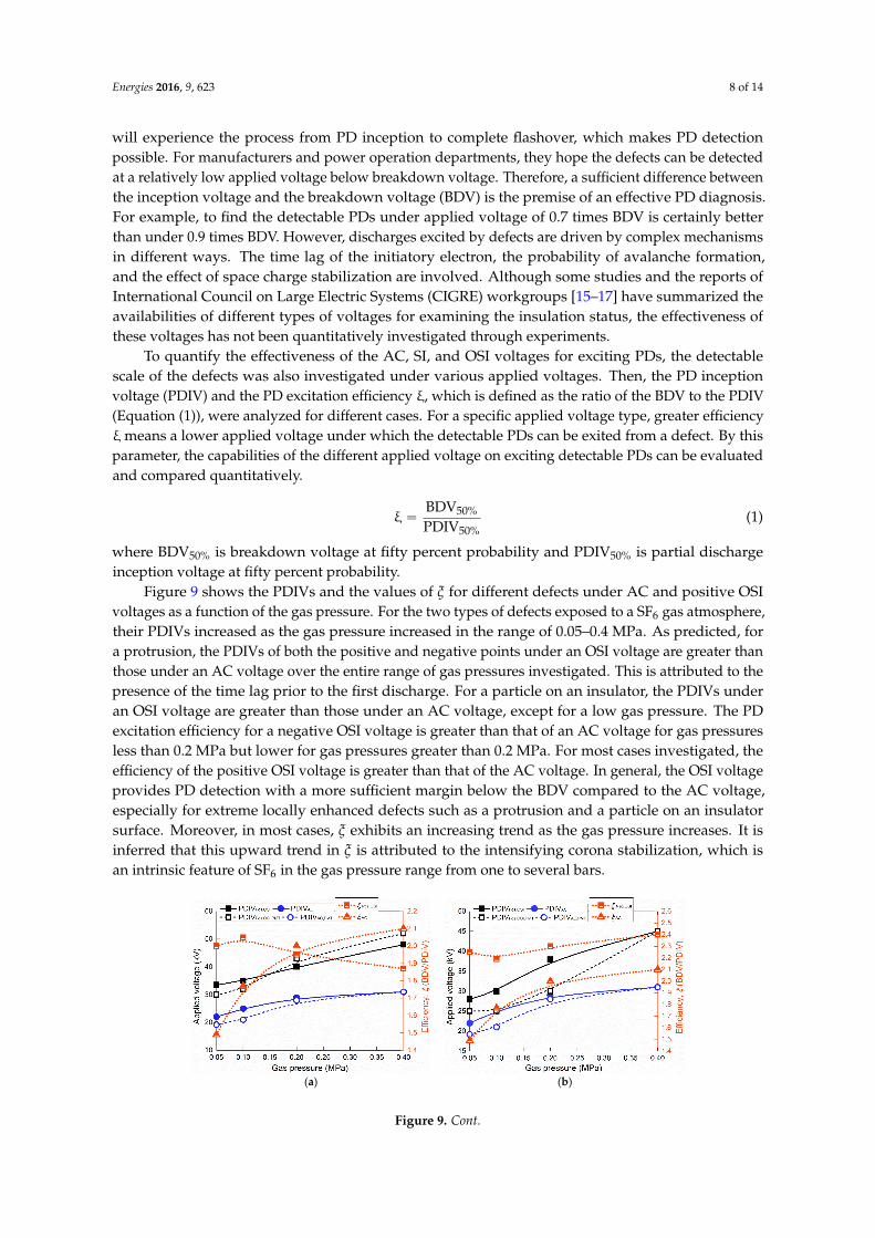
will experience the process from PD inception to complete flashover, which makes PD detectionpossible. For manufacturers and power operation departments, they hope the defects can be detectedat a relatively low applied voltage below breakdown voltage. Therefore, a sufficient difference betweenthe inception voltage and the breakdown voltage (BDV) is the premise of an effective PD diagnosis.For example, to find the detectable PDs under applied voltage of 0.7 times BDV is certainly betterthan under 0.9 times BDV. However, discharges excited by defects are driven by complex mechanismsin different ways. The time lag of the initiatory electron, the probability of avalanche formation,and the effect of space charge stabilization are involved. Although some studies and the reports ofInternational Council on Large Electric Systems (CIGRE) workgroups [15–17] have summarized theavailabilities of different types of voltages for examining the insulation status, the effectiveness ofthese voltages has not been quantitatively investigated through experiments.
To quantify the effectiveness of the AC, SI, and OSI voltages for exciting PDs, the detectablescale of the defects was also investigated under various applied voltages. Then, the PD inceptionvoltage (PDIV) and the PD excitation efficiency ξ, which is defined as the ratio of the BDV to the PDIV(Equation (1)), were analyzed for different cases. For a specific applied voltage type, greater efficiencyξ means a lower applied voltage under which the detectable PDs can be exited from a defect. By thisparameter, the capabilities of the different applied voltage on exciting detectable PDs can be evaluatedand compared quantitatively.
ξ “BDV50%
PDIV50%(1)
where BDV50% is breakdown voltage at fifty percent probability and PDIV50% is partial dischargeinception voltage at fifty percent probability.
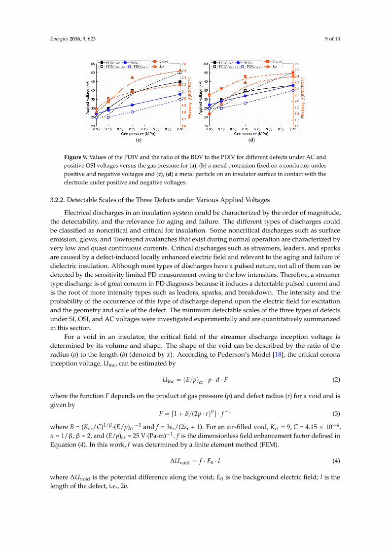
Figure 9 shows the PDIVs and the values of ξ for different defects under AC and positive OSIvoltages as a function of the gas pressure. For the two types of defects exposed to a SF6 gas atmosphere,their PDIVs increased as the gas pressure increased in the range of 0.05–0.4 MPa. As predicted, fora protrusion, the PDIVs of both the positive and negative points under an OSI voltage are greater thanthose under an AC voltage over the entire range of gas pressures investigated. This is attributed to thepresence of the time lag prior to the first discharge. For a particle on an insulator, the PDIVs underan OSI voltage are greater than those under an AC voltage, except for a low gas pressure. The PDexcitation efficiency for a negative OSI voltage is greater than that of an AC voltage for gas pressuresless than 0.2 MPa but lower for gas pressures greater than 0.2 MPa. For most cases investigated, theefficiency of the positive OSI voltage is greater than that of the AC voltage. In general, the OSI voltageprovides PD detection with a more sufficient margin below the BDV compared to the AC voltage,especially for extreme locally enhanced defects such as a protrusion and a particle on an insulatorsurface. Moreover, in most cases, ξ exhibits an increasing trend as the gas pressure increases. It isinferred that this upward trend in ξ is attributed to the intensifying corona stabilization, which isan intrinsic feature of SF6 in the gas pressure range from one to several bars.
Energies 2016, 9, 623 8 of 14
insulation will experience the process from PD inception to complete flashover, which makes PD
detection possible. For manufacturers and power operation departments, they hope the defects can
be detected at a relatively low applied voltage below breakdown voltage. Therefore, a sufficient
difference between the inception voltage and the breakdown voltage (BDV) is the premise of an
effective PD diagnosis. For example, to find the detectable PDs under applied voltage of 0.7 times
BDV is certainly better than under 0.9 times BDV. However, discharges excited by defects are driven
by complex mechanisms in different ways. The time lag of the initiatory electron, the probability of
avalanche formation, and the effect of space charge stabilization are involved. Although some studies
and the reports of International Council on Large Electric Systems (CIGRE) workgroups [15–17] have
summarized the availabilities of different types of voltages for examining the insulation status, the
effectiveness of these voltages has not been quantitatively investigated through experiments.
To quantify the effectiveness of the AC, SI, and OSI voltages for exciting PDs, the detectable scale
of the defects was also investigated under various applied voltages. Then, the PD inception voltage
(PDIV) and the PD excitation efficiency ξ, which is defined as the ratio of the BDV to the PDIV
(Equation (1)), were analyzed for different cases. For a specific applied voltage type, greater efficiency
ξ means a lower applied voltage under which the detectable PDs can be exited from a defect. By this
parameter, the capabilities of the different applied voltage on exciting detectable PDs can be
evaluated and compared quantitatively.
50%
50%
BDVξ=
PDIV (1)
where BDV50% is breakdown voltage at fifty percent probability and PDIV50% is partial discharge
inception voltage at fifty percent probability.
Figure 9 shows the PDIVs and the values of ξ for different defects under AC and positive OSI
voltages as a function of the gas pressure. For the two types of defects exposed to a SF6 gas
atmosphere, their PDIVs increased as the gas pressure increased in the range of 0.05–0.4 MPa. As
predicted, for a protrusion, the PDIVs of both the positive and negative points under an OSI voltage
are greater than those under an AC voltage over the entire range of gas pressures investigated. This
is attributed to the presence of the time lag prior to the first discharge. For a particle on an insulator,
the PDIVs under an OSI voltage are greater than those under an AC voltage, except for a low gas
pressure. The PD excitation efficiency for a negative OSI voltage is greater than that of an AC voltage
for gas pressures less than 0.2 MPa but lower for gas pressures greater than 0.2 MPa. For most cases
investigated, the efficiency of the positive OSI voltage is greater than that of the AC voltage. In
general, the OSI voltage provides PD detection with a more sufficient margin below the BDV
compared to the AC voltage, especially for extreme locally enhanced defects such as a protrusion and
a particle on an insulator surface. Moreover, in most cases, ξ exhibits an increasing trend as the gas
pressure increases. It is inferred that this upward trend in ξ is attributed to the intensifying corona
stabilization, which is an intrinsic feature of SF6 in the gas pressure range from one to several bars.
(a) (b)
Figure 9. Cont.
Energies 2016, 9, 623 9 of 14
Energies 2016, 9, 623 9 of 14
(c) (d)
Figure 9. Values of the PDIV and the ratio of the BDV to the PDIV for different defects under AC and
positive OSI voltages versus the gas pressure for (a), (b) a metal protrusion fixed on a conductor under
positive and negative voltages and (c), (d) a metal particle on an insulator surface in contact with the
electrode under positive and negative voltages.
3.2.2. Detectable Scales of the Three Defects under Various Applied Voltages
Electrical discharges in an insulation system could be characterized by the order of magnitude,
the detectability, and the relevance for aging and failure. The different types of discharges could be
classified as noncritical and critical for insulation. Some noncritical discharges such as surface
emission, glows, and Townsend avalanches that exist during normal operation are characterized by
very low and quasi continuous currents. Critical discharges such as streamers, leaders, and sparks
are caused by a defect-induced locally enhanced electric field and relevant to the aging and failure of
dielectric insulation. Although most types of discharges have a pulsed nature, not all of them can be
detected by the sensitivity limited PD measurement owing to the low intensities. Therefore, a
streamer type discharge is of great concern in PD diagnosis because it induces a detectable pulsed
current and is the root of more intensity types such as leaders, sparks, and breakdown. The intensity
and the probability of the occurrence of this type of discharge depend upon the electric field for
excitation and the geometry and scale of the defect. The minimum detectable scales of the three types
of defects under SI, OSI, and AC voltages were investigated experimentally and are quantitatively
summarized in this section.
For a void in an insulator, the critical field of the streamer discharge inception voltage is
determined by its volume and shape. The shape of the void can be described by the ratio of the radius
(a) to the length (b) (denoted by x). According to Pederson’s Model [18], the critical corona inception
voltage, Uinc, can be estimated by
crinc ( / )U E p p d F (2)
where the function F depends on the product of gas pressure (p) and defect radius (r) for a void and
is given by
1[1 / (2 ) ]nF B p r f (3)
where B = (Kcr/C)1/β·(E/p)cr−1 and f = 3εr/(2εr + 1). For an air-filled void, Kcr = 9, C = 4.15 × 10⁻⁴, n = 1/β,
β = 2, and (E/p)cr = 25 V·(Pa·m)−1. f is the dimensionless field enhancement factor defined in
Equation (4). In this work, f was determined by a finite element method (FEM).
0voidU f E l (4)
where ΔUvoid is the potential difference along the void; E0 is the background electric field; l is the
length of the defect, i.e., 2b.
To investigate the influence of void shape on electric field distribution, FEM numerical
calculations were performed on the voids in dielectric with different ratio x but the same volume. It
indicates that, the dimensionless field enhancement factor (f) defined in Equation (4) decreases
Figure 9. Values of the PDIV and the ratio of the BDV to the PDIV for different defects under AC andpositive OSI voltages versus the gas pressure for (a), (b) a metal protrusion fixed on a conductor underpositive and negative voltages and (c), (d) a metal particle on an insulator surface in contact with theelectrode under positive and negative voltages.
3.2.2. Detectable Scales of the Three Defects under Various Applied Voltages
Electrical discharges in an insulation system could be characterized by the order of magnitude,the detectability, and the relevance for aging and failure. The different types of discharges couldbe classified as noncritical and critical for insulation. Some noncritical discharges such as surfaceemission, glows, and Townsend avalanches that exist during normal operation are characterized byvery low and quasi continuous currents. Critical discharges such as streamers, leaders, and sparksare caused by a defect-induced locally enhanced electric field and relevant to the aging and failure ofdielectric insulation. Although most types of discharges have a pulsed nature, not all of them can bedetected by the sensitivity limited PD measurement owing to the low intensities. Therefore, a streamertype discharge is of great concern in PD diagnosis because it induces a detectable pulsed current andis the root of more intensity types such as leaders, sparks, and breakdown. The intensity and theprobability of the occurrence of this type of discharge depend upon the electric field for excitationand the geometry and scale of the defect. The minimum detectable scales of the three types of defectsunder SI, OSI, and AC voltages were investigated experimentally and are quantitatively summarizedin this section.
For a void in an insulator, the critical field of the streamer discharge inception voltage isdetermined by its volume and shape. The shape of the void can be described by the ratio of theradius (a) to the length (b) (denoted by x). According to Pederson’s Model [18], the critical coronainception voltage, Uinc, can be estimated by
Uinc “ pEpqcr ¨ p ¨ d ¨ F (2)
where the function F depends on the product of gas pressure (p) and defect radius (r) for a void and isgiven by
F “ r1` Bp2p ¨ rqns ¨ f ´1 (3)
where B = (Kcr/C)1/β¨(E/p)cr´1 and f = 3εr/(2εr + 1). For an air-filled void, Kcr = 9, C = 4.15 ˆ 10´4,
n = 1/β, β = 2, and (E/p)cr = 25 V¨(Pa¨m)´1. f is the dimensionless field enhancement factor defined inEquation (4). In this work, f was determined by a finite element method (FEM).
∆Uvoid “ f ¨ E0 ¨ l (4)
where ∆Uvoid is the potential difference along the void; E0 is the background electric field; l is thelength of the defect, i.e., 2b.

Energies 2016, 9, 623 10 of 14
To investigate the influence of void shape on electric field distribution, FEM numerical calculationswere performed on the voids in dielectric with different ratio x but the same volume. It indicatesthat, the dimensionless field enhancement factor (f ) defined in Equation (4) decreases approximatelylinearly with the increase of x. Based on Equation (3) and Equation (4), the critical corona inceptionvoltage (Uinc) is indicated to increase with the increase of the ratio (x). Figure 10 shows the fieldenhancement factor of the void and the streamer inception voltage versus x (the ratio of the radius(a) to the length (b)). It can be concluded that the prolate void in the insulator is more critical thanthe oblate void, even though they have the same volume because the former can induce a greaterLaplace field. It is noted that this inception voltage can be thought of as a necessary but not sufficientcondition for PD occurrence because the time lag for the initiatory electron should also be considered.In this study, two groups of void defect models with x = 0.5 and 2 are employed to investigate the PDintensity under different applied voltages.
Energies 2016, 9, 623 10 of 14
approximately linearly with the increase of x. Based on Equation (3) and Equation (4), the critical
corona inception voltage (Uinc) is indicated to increase with the increase of the ratio (x). Figure 10
shows the field enhancement factor of the void and the streamer inception voltage versus x (the ratio
of the radius (a) to the length (b)). It can be concluded that the prolate void in the insulator is more
critical than the oblate void, even though they have the same volume because the former can induce
a greater Laplace field. It is noted that this inception voltage can be thought of as a necessary but not
sufficient condition for PD occurrence because the time lag for the initiatory electron should also be
considered. In this study, two groups of void defect models with x = 0.5 and 2 are employed to
investigate the PD intensity under different applied voltages.
Figure 10. The influence of the void shape on the electric field in the void and the streamer inception
voltage. The volume of the void in the calculation is 1.57 mm3. The relative permittivities of the
insulator and the gas in the void are 4.1 and 1.0, respectively. The surface resistivity of the inner face
of the void is 10−20 Ω.
Gaseous voids were created at the center of the gap length between the upper and lower plate
electrodes to ensure a symmetrical field distribution. The polarity effect could not be exerted on the
PD events. Thus, a conclusion can be drawn by applying one polarity impulse to the sample. The
average PD magnitudes as a function of the void volume with prolate (x = 0.5) and oblate (x = 2)
shapes are shown in Figure 11a,b, respectively. Compared with the prolate voids, the oblate voids
produced PDs with a higher intensity, which were reflected in the pulse magnitudes (pC). The AC
voltage was not able to excite PDs above the detectable level (5 pC) for a small prolate void with a
volume of 1.5 mm3. In contrast, the PD under an OSI voltage has the greater average magnitude, even
for a void with a volume of 1.5 mm3; it is greater than 30 pC. The magnitudes of the PDs under an SI
voltage were between those under AC and OSI voltages for most cases, except for the oblate void
with a volume of 340 mm3, of which the PD magnitude is greater than that of the OSI voltage. In
general, the PD intensity shows an obvious increase by two orders of magnitude as the void volume
increases from 1.5 to 340 mm3.
It is noted that a tiny void in an actual insulator is not analogous to the electrode spacing in real
equipment. The signal induced in the coupling circuit is immeasurably low and thus obscured by
noise. In reality, a detectable void in real scale equipment is larger than expected.
Figure 10. The influence of the void shape on the electric field in the void and the streamer inceptionvoltage. The volume of the void in the calculation is 1.57 mm3. The relative permittivities of theinsulator and the gas in the void are 4.1 and 1.0, respectively. The surface resistivity of the inner face ofthe void is 10´20 Ω.
Gaseous voids were created at the center of the gap length between the upper and lower plateelectrodes to ensure a symmetrical field distribution. The polarity effect could not be exerted on the PDevents. Thus, a conclusion can be drawn by applying one polarity impulse to the sample. The averagePD magnitudes as a function of the void volume with prolate (x = 0.5) and oblate (x = 2) shapes areshown in Figure 11a,b, respectively. Compared with the prolate voids, the oblate voids produced PDswith a higher intensity, which were reflected in the pulse magnitudes (pC). The AC voltage was notable to excite PDs above the detectable level (5 pC) for a small prolate void with a volume of 1.5 mm3.In contrast, the PD under an OSI voltage has the greater average magnitude, even for a void witha volume of 1.5 mm3; it is greater than 30 pC. The magnitudes of the PDs under an SI voltage werebetween those under AC and OSI voltages for most cases, except for the oblate void with a volumeof 340 mm3, of which the PD magnitude is greater than that of the OSI voltage. In general, the PDintensity shows an obvious increase by two orders of magnitude as the void volume increases from 1.5to 340 mm3.
It is noted that a tiny void in an actual insulator is not analogous to the electrode spacing in realequipment. The signal induced in the coupling circuit is immeasurably low and thus obscured bynoise. In reality, a detectable void in real scale equipment is larger than expected.
Energies 2016, 9, 623 11 of 14Energies 2016, 9, 623 11 of 14
(a) x = 0.5 (b) x = 2
Figure 11. Average PD magnitude versus the volume of the void in the insulator. The OSI, SI, and
50 Hz AC voltages applied to the samples are equal to 1.6 times the PDIV.
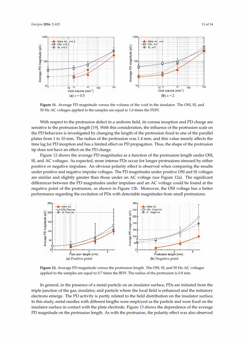
With respect to the protrusion defect in a uniform field, its corona inception and PD charge are
sensitive to the protrusion length [19]. With this consideration, the influence of the protrusion scale
on the PD behaviors is investigated by changing the length of the protrusion fixed to one of the
parallel plates from 1 to 10 mm. The radius of the protrusion was 1.4 mm, and this value merely
affects the time lag for PD inception and has a limited effect on PD propagation. Thus, the shape of
the protrusion tip does not have an effect on the PD charge.
Figure 12 shows the average PD magnitudes as a function of the protrusion length under OSI,
SI, and AC voltages. As expected, more intense PDs occur for longer protrusions stressed by either
positive or negative impulses. An obvious polarity effect is observed when comparing the results
under positive and negative impulse voltages. The PD magnitudes under positive OSI and SI voltages
are similar and slightly greater than those under an AC voltage (see Figure 12a). The significant
differences between the PD magnitudes under impulses and an AC voltage could be found at the
negative point of the protrusion, as shown in Figure 12b. Moreover, the OSI voltage has a better
performance regarding the excitation of PDs with detectable magnitudes from small protrusions.
(a) Positive point (b) Negative point
Figure 12. Average PD magnitude versus the protrusion length. The OSI, SI, and 50 Hz AC voltages
applied to the samples are equal to 0.7 times the BDV. The radius of the protrusion is 0.8 mm.
In general, in the presence of a metal particle on an insulator surface, PDs are initiated from the
triple junction of the gas, insulator, and particle where the local field is enhanced and the initiatory
electrons emerge. The PD activity is partly related to the field distribution on the insulator surface. In
this study, metal needles with different lengths were employed as the particle and were fixed on the
insulator surface in contact with the plate electrode. Figure 13 shows the dependence of the average
PD magnitude on the protrusion length. As with the protrusion, the polarity effect was also observed
for the particle on the insulator surface. The PD magnitudes for various protrusion lengths under an
OSI voltage were much greater than those under SI and AC voltages. In the test, all of the types of
Figure 11. Average PD magnitude versus the volume of the void in the insulator. The OSI, SI, and50 Hz AC voltages applied to the samples are equal to 1.6 times the PDIV.
With respect to the protrusion defect in a uniform field, its corona inception and PD charge aresensitive to the protrusion length [19]. With this consideration, the influence of the protrusion scale onthe PD behaviors is investigated by changing the length of the protrusion fixed to one of the parallelplates from 1 to 10 mm. The radius of the protrusion was 1.4 mm, and this value merely affects thetime lag for PD inception and has a limited effect on PD propagation. Thus, the shape of the protrusiontip does not have an effect on the PD charge.
Figure 12 shows the average PD magnitudes as a function of the protrusion length under OSI,SI, and AC voltages. As expected, more intense PDs occur for longer protrusions stressed by eitherpositive or negative impulses. An obvious polarity effect is observed when comparing the resultsunder positive and negative impulse voltages. The PD magnitudes under positive OSI and SI voltagesare similar and slightly greater than those under an AC voltage (see Figure 12a). The significantdifferences between the PD magnitudes under impulses and an AC voltage could be found at thenegative point of the protrusion, as shown in Figure 12b. Moreover, the OSI voltage has a betterperformance regarding the excitation of PDs with detectable magnitudes from small protrusions.
Energies 2016, 9, 623 11 of 14
(a) x = 0.5 (b) x = 2
Figure 11. Average PD magnitude versus the volume of the void in the insulator. The OSI, SI, and
50 Hz AC voltages applied to the samples are equal to 1.6 times the PDIV.
With respect to the protrusion defect in a uniform field, its corona inception and PD charge are
sensitive to the protrusion length [19]. With this consideration, the influence of the protrusion scale
on the PD behaviors is investigated by changing the length of the protrusion fixed to one of the
parallel plates from 1 to 10 mm. The radius of the protrusion was 1.4 mm, and this value merely
affects the time lag for PD inception and has a limited effect on PD propagation. Thus, the shape of
the protrusion tip does not have an effect on the PD charge.
Figure 12 shows the average PD magnitudes as a function of the protrusion length under OSI,
SI, and AC voltages. As expected, more intense PDs occur for longer protrusions stressed by either
positive or negative impulses. An obvious polarity effect is observed when comparing the results
under positive and negative impulse voltages. The PD magnitudes under positive OSI and SI voltages
are similar and slightly greater than those under an AC voltage (see Figure 12a). The significant
differences between the PD magnitudes under impulses and an AC voltage could be found at the
negative point of the protrusion, as shown in Figure 12b. Moreover, the OSI voltage has a better
performance regarding the excitation of PDs with detectable magnitudes from small protrusions.
(a) Positive point (b) Negative point
Figure 12. Average PD magnitude versus the protrusion length. The OSI, SI, and 50 Hz AC voltages
applied to the samples are equal to 0.7 times the BDV. The radius of the protrusion is 0.8 mm.
In general, in the presence of a metal particle on an insulator surface, PDs are initiated from the
triple junction of the gas, insulator, and particle where the local field is enhanced and the initiatory
electrons emerge. The PD activity is partly related to the field distribution on the insulator surface. In
this study, metal needles with different lengths were employed as the particle and were fixed on the
insulator surface in contact with the plate electrode. Figure 13 shows the dependence of the average
PD magnitude on the protrusion length. As with the protrusion, the polarity effect was also observed
for the particle on the insulator surface. The PD magnitudes for various protrusion lengths under an
OSI voltage were much greater than those under SI and AC voltages. In the test, all of the types of
Figure 12. Average PD magnitude versus the protrusion length. The OSI, SI, and 50 Hz AC voltagesapplied to the samples are equal to 0.7 times the BDV. The radius of the protrusion is 0.8 mm.
In general, in the presence of a metal particle on an insulator surface, PDs are initiated from thetriple junction of the gas, insulator, and particle where the local field is enhanced and the initiatoryelectrons emerge. The PD activity is partly related to the field distribution on the insulator surface.In this study, metal needles with different lengths were employed as the particle and were fixed on theinsulator surface in contact with the plate electrode. Figure 13 shows the dependence of the averagePD magnitude on the protrusion length. As with the protrusion, the polarity effect was also observed
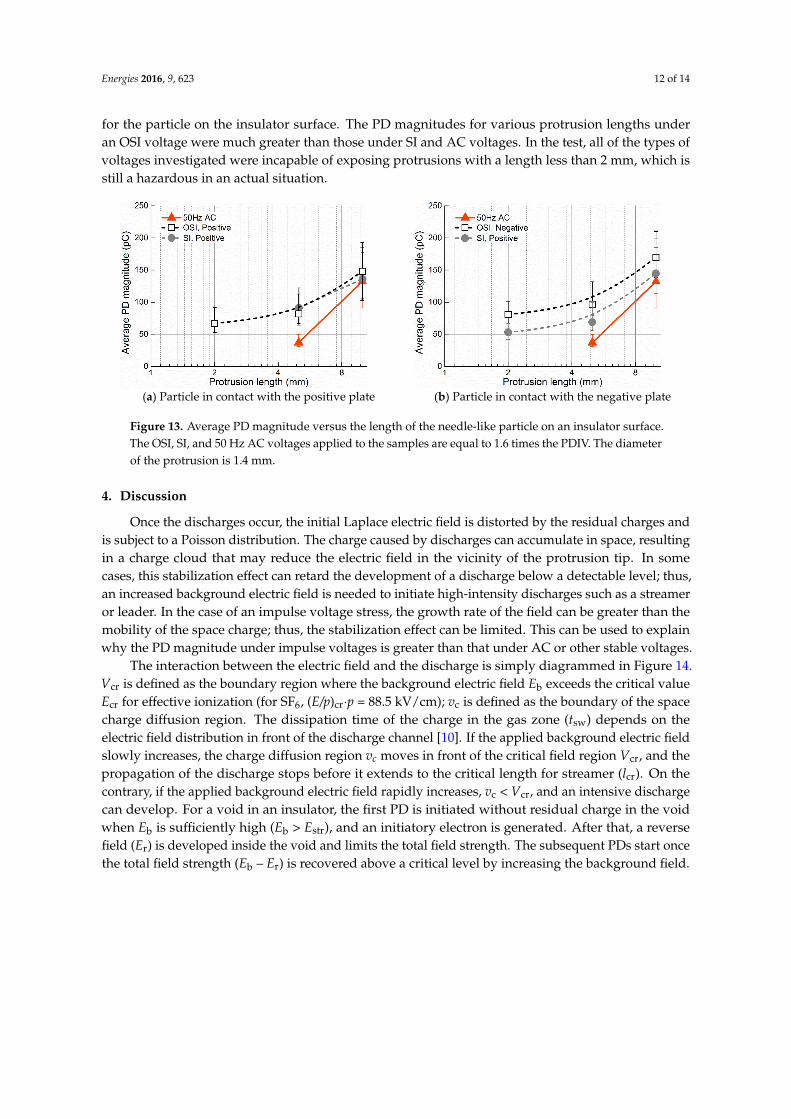
Energies 2016, 9, 623 12 of 14
for the particle on the insulator surface. The PD magnitudes for various protrusion lengths underan OSI voltage were much greater than those under SI and AC voltages. In the test, all of the types ofvoltages investigated were incapable of exposing protrusions with a length less than 2 mm, which isstill a hazardous in an actual situation.
Energies 2016, 9, 623 12 of 14
voltages investigated were incapable of exposing protrusions with a length less than 2 mm, which is
still a hazardous in an actual situation.
(a) Particle in contact with the positive plate (b) Particle in contact with the negative plate
Figure 13. Average PD magnitude versus the length of the needle-like particle on an insulator surface.
The OSI, SI, and 50 Hz AC voltages applied to the samples are equal to 1.6 times the PDIV. The
diameter of the protrusion is 1.4 mm.
4. Discussion
Once the discharges occur, the initial Laplace electric field is distorted by the residual charges
and is subject to a Poisson distribution. The charge caused by discharges can accumulate in space,
resulting in a charge cloud that may reduce the electric field in the vicinity of the protrusion tip. In
some cases, this stabilization effect can retard the development of a discharge below a detectable
level; thus, an increased background electric field is needed to initiate high-intensity discharges such
as a streamer or leader. In the case of an impulse voltage stress, the growth rate of the field can be
greater than the mobility of the space charge; thus, the stabilization effect can be limited. This can be
used to explain why the PD magnitude under impulse voltages is greater than that under AC or other
stable voltages.
The interaction between the electric field and the discharge is simply diagrammed in Figure 14.
Vcr is defined as the boundary region where the background electric field Eb exceeds the critical value
Ecr for effective ionization (for SF6, (E/p)cr·p = 88.5 kV/cm); vc is defined as the boundary of the space
charge diffusion region. The dissipation time of the charge in the gas zone (tsw) depends on the electric
field distribution in front of the discharge channel [10]. If the applied background electric field slowly
increases, the charge diffusion region vc moves in front of the critical field region Vcr, and the
propagation of the discharge stops before it extends to the critical length for streamer (lcr). On the
contrary, if the applied background electric field rapidly increases, vc < Vcr, and an intensive discharge
can develop. For a void in an insulator, the first PD is initiated without residual charge in the void
when Eb is sufficiently high (Eb > Estr), and an initiatory electron is generated. After that, a reverse
field (Er) is developed inside the void and limits the total field strength. The subsequent PDs start
once the total field strength (Eb – Er) is recovered above a critical level by increasing the
background field.
Figure 13. Average PD magnitude versus the length of the needle-like particle on an insulator surface.The OSI, SI, and 50 Hz AC voltages applied to the samples are equal to 1.6 times the PDIV. The diameterof the protrusion is 1.4 mm.
4. Discussion
Once the discharges occur, the initial Laplace electric field is distorted by the residual charges andis subject to a Poisson distribution. The charge caused by discharges can accumulate in space, resultingin a charge cloud that may reduce the electric field in the vicinity of the protrusion tip. In somecases, this stabilization effect can retard the development of a discharge below a detectable level; thus,an increased background electric field is needed to initiate high-intensity discharges such as a streameror leader. In the case of an impulse voltage stress, the growth rate of the field can be greater than themobility of the space charge; thus, the stabilization effect can be limited. This can be used to explainwhy the PD magnitude under impulse voltages is greater than that under AC or other stable voltages.
The interaction between the electric field and the discharge is simply diagrammed in Figure 14.Vcr is defined as the boundary region where the background electric field Eb exceeds the critical valueEcr for effective ionization (for SF6, (E/p)cr¨p = 88.5 kV/cm); vc is defined as the boundary of the spacecharge diffusion region. The dissipation time of the charge in the gas zone (tsw) depends on theelectric field distribution in front of the discharge channel [10]. If the applied background electric fieldslowly increases, the charge diffusion region vc moves in front of the critical field region Vcr, and thepropagation of the discharge stops before it extends to the critical length for streamer (lcr). On thecontrary, if the applied background electric field rapidly increases, vc < Vcr, and an intensive dischargecan develop. For a void in an insulator, the first PD is initiated without residual charge in the voidwhen Eb is sufficiently high (Eb > Estr), and an initiatory electron is generated. After that, a reversefield (Er) is developed inside the void and limits the total field strength. The subsequent PDs start oncethe total field strength (Eb – Er) is recovered above a critical level by increasing the background field.

Energies 2016, 9, 623 13 of 14Energies 2016, 9, 623 13 of 14
Figure 14. Comparison of PD propagation affected by the space charge under a slowly varying
voltage and an impulse voltage.
5. Conclusions
PD detection under impulse voltage conditions, has been investigated based on three artificial
test models in terms of the measurement method, test object, and PD behavior. The general PD
sequence features were briefly summarized by exemplifying the typical PD pulses of different defects
under an OSI voltage. The single pulse, multiple pulses, and the reverse polarity pulse with different
mechanisms were considered to be the main components of the PD sequences. Although the PDIVs
under an OSI voltage were greater than those under an AC voltage over entire range of gas pressures
investigated, the PD excitation efficiency, i.e., the ratio of the BDV to the PDIV, under an OSI voltage
is greater than that under an AC voltage for most cases, which means PD detection under an OSI
voltage has a more sufficient margin below the BDV. It was also found that the OSI voltage has good
performance for the excitation of PDs from a small-scale defect with more detectable magnitudes. In
contrast, an AC voltage is incapable of finding some defects even with hazardous scales. The good
detectability imparted by the impulse voltages accounts for the weakened corona stabilization under
an impulse. The authors believe that, in the case of an impulse voltage stress, the growth rate of the
field can be greater than the mobility of the space charge; thus, the stabilization effect can be limited.
Acknowledgments: The authors would like to thank the National Natural Science Foundation of China (Grant
No. 51507130), China Postdoctoral Science Foundation (Grant No. 2014M560777), Special China Postdoctoral
Science Foundation (Grant No. 2016-11-141158), Shaanxi International Cooperation and Exchanges Foundation
(Grant No. 2016KW-072) and Fundamental Research Funds for the Central Universities.
Author Contributions: MR and MD conceived and designed the experiments; CZ and JZ performed the
experiments and relevant simulations; MR and CZ analyzed the data; MR wrote the paper.
Conflicts of Interest: The authors declare no conflict of interest.
References
1. CIGRE Joint Task Force. Partial Discharge Detection System for GIS: Sensitivity Verification for the UHF
Method and the Acoustic Method. Electra 1999, 183, 75–87.
2. Takahashi, T.; Yamada, T.; Hayakawa, N.; Okubo, H. Space charge behavior in SF6 gas and sequential
generation of PD pulses. IEEE Trans. Dielectr. Electr. Insul. 2000, 7, 141–145.
Figure 14. Comparison of PD propagation affected by the space charge under a slowly varying voltageand an impulse voltage.
5. Conclusions
PD detection under impulse voltage conditions, has been investigated based on three artificialtest models in terms of the measurement method, test object, and PD behavior. The general PDsequence features were briefly summarized by exemplifying the typical PD pulses of different defectsunder an OSI voltage. The single pulse, multiple pulses, and the reverse polarity pulse with differentmechanisms were considered to be the main components of the PD sequences. Although the PDIVsunder an OSI voltage were greater than those under an AC voltage over entire range of gas pressuresinvestigated, the PD excitation efficiency, i.e., the ratio of the BDV to the PDIV, under an OSI voltageis greater than that under an AC voltage for most cases, which means PD detection under an OSIvoltage has a more sufficient margin below the BDV. It was also found that the OSI voltage has goodperformance for the excitation of PDs from a small-scale defect with more detectable magnitudes.In contrast, an AC voltage is incapable of finding some defects even with hazardous scales. The gooddetectability imparted by the impulse voltages accounts for the weakened corona stabilization underan impulse. The authors believe that, in the case of an impulse voltage stress, the growth rate of thefield can be greater than the mobility of the space charge; thus, the stabilization effect can be limited.
Acknowledgments: The authors would like to thank the National Natural Science Foundation of China (GrantNo. 51507130), China Postdoctoral Science Foundation (Grant No. 2014M560777), Special China PostdoctoralScience Foundation (Grant No. 2016-11-141158), Shaanxi International Cooperation and Exchanges Foundation(Grant No. 2016KW-072) and Fundamental Research Funds for the Central Universities.
Author Contributions: M.R. and M.D. conceived and designed the experiments; C.Z. and J.Z. performed theexperiments and relevant simulations; M.R. and C.Z. analyzed the data; M.R. wrote the paper.
Conflicts of Interest: The authors declare no conflict of interest.
References
1. CIGRE Joint Task Force. Partial Discharge Detection System for GIS: Sensitivity Verification for the UHFMethod and the Acoustic Method. Electra 1999, 183, 75–87.

Energies 2016, 9, 623 14 of 14
2. Takahashi, T.; Yamada, T.; Hayakawa, N.; Okubo, H. Space charge behavior in SF6 gas and sequentialgeneration of PD pulses. IEEE Trans. Dielectr. Electr. Insul. 2000, 7, 141–145. [CrossRef]
3. Hinterholzer, T.; Boeck, W. Breakdown in SF6 influenced by corona-stabilization. Electr. Insul. Dielectr. Phenom.2000, 1, 413–416.
4. High-Voltage Test Techniques-Part 3: Definitions and Requirements for On-site Testing; International ElectrotechnicalCommission (IEC): Geneva, Switzerland, 2006.
5. Meijer, S.; Gulski, E.; Smit, J.J.; Kanters, A.J.L. Risk assessment of fixed defects in GIS under different voltagewave shapes. In Proceedings of 18th International Conference and Exhibition on Electricity Distribution,Turin, Italy, 6–9 June 2005.
6. Okabe, S.; Yuasa, S.; Kaneko, S.; Ueta, G. Evaluation of breakdown characteristics of gas insulated switchgearsfor non-standard lightning impulse waveforms method-method for converting non-standard lightningimpulses waveforms into standard impulse waveforms. IEEE Trans. Dielectr. Electr. Insul. 2009, 16, 42–51.[CrossRef]
7. Anis, H.; Srivastava, K.D. Breakdown of rod-plane gaps in SF6 under positive switching impulses. IEEE Trans.Power App. Syst. 1982, 101, 537–546. [CrossRef]
8. Niemeyer, L.; Ullrich, L.; Wiegart, N. The mechanism of leader breakdown in electronegative gases.IEEE Trans. Electr. Insul. 1989, 24, 309–324. [CrossRef]
9. Hayakawa, N.; Yoshitake, Y.; Koshino, N.; Ueda, T.; Okubo, H. Impulse partial discharge characteristics andtheir mechanisms under non-uniform electric field in N2/SF6 gas mixture. IEEE Trans. Dielectr. Electr. Insul.2005, 12, 1035–1042. [CrossRef]
10. Wiegart, N.; Niemeyer, L.; Pinnekamp, F.; Boeck, W.; Kindersberger, J.; Morrow, R.; Zaengl, W.; Zwicky, M.;Gallimberti, I.; Boggs, S.A. Inhomogeneous field breakdown in GIS-the prediction of breakdown probabilitiesand voltages. III. Discharge development in SF6 and computer model of breakdown. IEEE Trans. Power Deliv.1988, 3, 939–946. [CrossRef]
11. Niemeyer, L. A generalized approach to partial discharge in modeling. IEEE Trans. Dielectr. Electr. Insul.1995, 2, 510–528. [CrossRef]
12. Ren, M.; Dong, M.; Xiao, Z.; Qiu, A. Partial discharge pulses at artificial protrusions in SF6 under negativeIEC 60060-3 standard impulses. IEEE Trans. Dielectr. Electr. Insul. 2014, 21, 273–283. [CrossRef]
13. Ren, M.; Dong, M.; Xiao, Z.; Qiu, A. Partial discharges in SF6 filled void under standard aperidic andoscillating switching impulses. IEEE Trans. Dielectr. Electr. Insul. 2014, 21, 262–272. [CrossRef]
14. Densley, R.J.; Salvage, B. Partial Discharges in Gaseous Cavities in Solid Dielectrics under Impulse VoltageConditions. IEEE Trans. Electr. Insul. 1971, EI-6, 54–62. [CrossRef]
15. CIGRE Working Group. Insulation coordination of GIS: Return of experience, on site tests and diagnostictechniques. Electra 1998, 176, 67–95.
16. Haller, R.; Hauschild, W.; Mosch, W. High-voltage field testing of GIS from a physical view-point.In Proceedings of the Second International Conference on Properties and Applications of Properties andApplications of Dielectric Materials, Beijing, China, 12–16 September 1988.
17. Kornhuber, S.; Boltze, M.; Haller, R.; Mraz, P.; Pihera, J. PD behavior of basic test arrangements underdifferent measurement conditions. In Proceedings of the International Conference on Condition Monitoringand Diagnosis (CMD), Bali, Indonesia, 23–27 September 2012.
18. Crichton, G.C.; Karlsson, P.W.; Pedersen, A. Partial Discharges in Ellipsoidal and Spheroidal Voids.IEEE Trans. Electr. Insul. 1989, 24, 335–342. [CrossRef]
19. Seeger, M.; Niemeyer, L.; Bujotzek, M. Partial discharges and breakdown at protrusions in uniformbackground fields in SF6. J. Phys. D: Appl. Phys. 2008, 41, 185204. [CrossRef]
© 2016 by the authors; licensee MDPI, Basel, Switzerland. This article is an open accessarticle distributed under the terms and conditions of the Creative Commons Attribution(CC-BY) license (http://creativecommons.org/licenses/by/4.0/).