Paralleling GaN HEMTs for Diode-free Bridge Power Converters
7
TO-220 Package G S D S Fig. 1: GaN hybrid HEMT incorporating a LV normally-off Si FET and an HV normally-on GaN HEMT (a) to achieve a combined, normally-off device (b) in a Quiet-Tab TO-220 package (c). Paralleling GaN HEMTs for Diode-free Bridge Power Converters Zhan Wang, Yifeng Wu, Jim Honea, Liang Zhou Power Electronics Circuit Group, Transphorm Inc., Goleta, CA, USA Email: {zhanwang, ywu, jhonea, lzhou}@transphormusa.com Abstract— GaN devices have superior performance over Si- based devices, and high voltage normally-off GaN HEMTs with cascode structure have been available for industry application as they can be easily driven by mature commercial Si-MOSFET drivers. Due to the very fast switching speed, the PCB layout and driver circuit design should be very careful to keep the parasitic parameters as small as possible. Paralleling semiconductor devices is an effective and simple way for higher power application. It is very challenging to parallel GaN HEMTs in hard-switching bridge power converter application, especially for discrete leaded package devices. However, leaded packages are still dominant in industrial applications because of their simplicity for PCB assembly and capability for a wide variety of heat-sinking techniques. In this paper, a solution to paralleling GaN HEMTs for diode-free bridge power converters is proposed, and GaN device driver design is discussed. The partial phase method is also suitable for the low power application to improve the efficiency. Simulations of driving circuit and experimental results on a 5 kW half bridge operating in synchronous boost mode with 4 paralleling GaN HEMTs are provided for validation. Keywords—GaN; HEMT; leaded package; parallel; bridge I. INTRODUCTION Currently widely used in LEDs, Gallium Nitride (GaN) is the next generation in power electronics. The GaN high electron mobility transistor (HEMT) combines low switching and conduction losses, offering reduced energy loss of more than 50 percent compared to conventional silicon-based power conversion designs. Transphorm Inc. has established the industry’s first qualified 600-V GaN device platform with its TPH3006 GaN HEMT. The TO-220-packaged device features R ds(on) of 150 mΩ, Q rr of 56 nC and high-frequency switching capability that enables compact lower cost systems [1], as shown in Fig. 1. Not only applicable for high frequency DC- DC converter applications [2], GaN HEMTs are also promising for replacing Si-IGBTs in AC-DC/ DC-AC applications, such as PFC, PV inverter and motor drive applications [3-5]. Two types of TO-220 600-V GaN HEMTs are provided which have Source Kelvin Tab and Drain Tab, respectively. Soldering the tab directly to the PCB is a good way for eliminating the lead parasitic inductance so as to reduce ringing on gate and switching node [6], but it is not widely used in industry due to the issues of reflow soldering and heat dissipation limitation. For the high power application, low thermal resistance heat sinks are necessary to mount on the tabs of GaN HEMTs, and PCB layout with leads connection should be studied. Moreover, paralleling GaN HEMTs is also attractive for high power applications [7-9]. However, it is very challenging for paralleling discrete GaN devices as the parasitic inductance increases with the increasing footprint. In this paper, a basic half bridge along with driver circuit using discrete GaN HEMTs is analyzed, and then two and 2N devices in parallel are discussed. Simple and robust solution without PCB layout and thermal management limitation is proposed. A partial phase operation mode is also applicable for this method for improving the efficiency at low power. II. INVESTIGATION OF DRIVING CIRCUIT OF HALF BRIDGE GAN HEMTS Fig. 2 shows a half bridge circuit schematic with half-
Transcript of Paralleling GaN HEMTs for Diode-free Bridge Power Converters

TO-220 Package
G S
D
S
Fig. 1: GaN hybrid HEMT incorporating a LV normally-off Si FET and an HV normally-on GaN HEMT (a) to achieve a combined, normally-off device (b) in a Quiet-Tab TO-220 package (c).
Paralleling GaN HEMTs for Diode-free Bridge Power Converters
Zhan Wang, Yifeng Wu, Jim Honea, Liang Zhou Power Electronics Circuit Group,
Transphorm Inc., Goleta, CA, USA
Email: zhanwang, ywu, jhonea, [email protected]
Abstract— GaN devices have superior performance over Si-based devices, and high voltage normally-off GaN HEMTs with cascode structure have been available for industry application as they can be easily driven by mature commercial Si-MOSFET drivers. Due to the very fast switching speed, the PCB layout and driver circuit design should be very careful to keep the parasitic parameters as small as possible. Paralleling semiconductor devices is an effective and simple way for higher power application. It is very challenging to parallel GaN HEMTs in hard-switching bridge power converter application, especially for discrete leaded package devices. However, leaded packages are still dominant in industrial applications because of their simplicity for PCB assembly and capability for a wide variety of heat-sinking techniques. In this paper, a solution to paralleling GaN HEMTs for diode-free bridge power converters is proposed, and GaN device driver design is discussed. The partial phase method is also suitable for the low power application to improve the efficiency. Simulations of driving circuit and experimental results on a 5 kW half bridge operating in synchronous boost mode with 4 paralleling GaN HEMTs are provided for validation.
Keywords—GaN; HEMT; leaded package; parallel; bridge
I. INTRODUCTION Currently widely used in LEDs, Gallium Nitride (GaN) is
the next generation in power electronics. The GaN high electron mobility transistor (HEMT) combines low switching and conduction losses, offering reduced energy loss of more than 50 percent compared to conventional silicon-based power conversion designs. Transphorm Inc. has established the industry’s first qualified 600-V GaN device platform with its TPH3006 GaN HEMT. The TO-220-packaged device features Rds(on) of 150 mΩ, Qrr of 56 nC and high-frequency switching capability that enables compact lower cost systems [1], as shown in Fig. 1. Not only applicable for high frequency DC-DC converter applications [2], GaN HEMTs are also promising for replacing Si-IGBTs in AC-DC/ DC-AC applications, such as PFC, PV inverter and motor drive applications [3-5].
Two types of TO-220 600-V GaN HEMTs are provided which have Source Kelvin Tab and Drain Tab, respectively. Soldering the tab directly to the PCB is a good way for eliminating the lead parasitic inductance so as to reduce ringing on gate and switching node [6], but it is not widely used in industry due to the issues of reflow soldering and heat
dissipation limitation. For the high power application, low thermal resistance heat sinks are necessary to mount on the tabs of GaN HEMTs, and PCB layout with leads connection should be studied. Moreover, paralleling GaN HEMTs is also attractive for high power applications [7-9]. However, it is very challenging for paralleling discrete GaN devices as the parasitic inductance increases with the increasing footprint.
In this paper, a basic half bridge along with driver circuit using discrete GaN HEMTs is analyzed, and then two and 2N devices in parallel are discussed. Simple and robust solution without PCB layout and thermal management limitation is proposed. A partial phase operation mode is also applicable for this method for improving the efficiency at low power.
II. INVESTIGATION OF DRIVING CIRCUIT OF HALF BRIDGE GAN HEMTS
Fig. 2 shows a half bridge circuit schematic with half-

(a)
(b)
Fig. 2: Half bridge GaN HEMTs test circuit: (a) schematic, J1 is for low side device hard switching test, J2 is for high side hard switching test; (b) Half bridge test circuit back-to-back 2 layer layout: switching node connection is minimized, while low side gate loop trace is longer than high side.
(a) (b)
02468101214161820
0
20
40
60
80
100
120
140
0.00 2.00 4.00 6.00 8.00 10.00 12.00
dv/dt
di/dt (rising)
di/dt (falling)
-40-30-20-10010203040
-100
0
100
200
300
400
500
600
1.99 2.00 2.01 2.02
VdsiLid
(c) (d)
Fig. 3: Multi-pulse hard-switching test, fsw = 1MHz, Npulse = 8, fcycle = 30 ms. (a) High side hard-switching to 41.6 A; (b) Low side hard-switching to 27 A. (c) Dv/dt and di/dt rating from 0 A to 10 A; (d) Cross over time is 13.9 ns at iL = 10 A.
bridge boot-strap driver. Due to the very high di/dt rating, Si8230/1BB driver from Silicon-Lab is selected as it consists of a half bridge MOSFETs driver and digital isolator, which provides best-in-class noise immunity thanks to its less than 2 pF coupling capacitance [10].
The TO220 package unavoidably adds inductance in the source lead, as shown in Fig. 2 (a). This inductance cannot be further reduced, and so its impact must be recognized and mitigated. The normal expectation when a voltage signal develops across a source impedance is that it will subtract from the gate-drive voltage and slow the turn on. Slowing the di/dt transition by reducing Ig will indeed reduce the corresponding source voltage during that part of the turn-on transient. Using a gate resistor in the place of Zg in Fig. 2 would accomplish this. A gate resistor will not, however, provide the additional function of limiting slew rate at the switching node: d(Vds)/dt. This is because the feedback capacitance, Crss, of the cascode combination is so low. Simply choosing a gate driver with a lower output current is a better way to limit Ig and di/dt. It is found that a small SMD ferrite bead effectively opposes such transient current and inhibits coupling of the signal [11], although the voltage waveform on the gate pin is not obviously damped.
A ferrite bead MMZ2012D121B from TDK is selected as Zg, which has nearly zero dc resistance and 120 Ω impedance at 100 MHz, and a 15 Ω/ 0.5 W resistor as Rb for preventing circuit from impacting by inrush current caused by undershoot voltage spike of high side device switching. Fig. 3 (a) shows the high side device can hard switch at 41.6A with Vds undershoot no more than -100V; Fig. 3 (b) shows the low side device can hard switch at 27A with Vds spikes no more than 600V. The dv/dt and di/dt are over 120 V/ns and 10 A/ns, respectively, which mean the switching speed does not slow down and switching loss will keep low at high switching frequency. Although the back-to-back placement provides a very compact layout, the possible reason that low side device blows up at 31A hard-switching test is the gate circuit loop is larger compared to high side device as shown in Fig. 2 (b).
III. INVESTIGATION OF DISCRETE GAN HEMTS IN PARALLEL
It becomes more difficult to parallel discrete GaN devices for bridge power converters, because the parasitic inductance and capacitance on PCB layout will increase due to the foot prints’ area increasing. In [12], four paralleling GaN HEMTs are proposed for high power boost converter application. The layout is very compact to minimize the parasitic inductance and the driver length should be equal to make the switching time symmetrical. For the half bridge application with GaN HEMTs, the switching stress will be higher than unidirectional boost converter using SiC diodes, so voltage ringing caused by common source inductance is more severe. Since the threshold gate voltage of MOSFET is only 2.1 V, the oscillation voltage spikes due to interference of high side turn off may make the low side device fault turn on. Under this consideration, negative voltage bias on the gate driver is proposed in the

(a)
(b) (c)
Fig. 4: Half bridge circuit with directly paralleling TO220 GaN HEMTs: (a) compact and symmetrical 4 layer layout; (b) High side hard-switching up to 51.6 A; (c) Low side hard-switching up to 52A.
Driver
In1
In2
LA
Q1_1
Q2_1
IoA
Vo
PWM1
PWM1
Lf
LBLA=LB<<Lf
Driver
Q1_3
Q2_3
Q1_4
Q2_4
Q1_2
Q2_1
In1
In2IoB
Vbus+
Vbus+
DC
Vbus+
400V
PGND
Cbus
Cdecouple
Io
A
B
(a)
(b)
Fig. 5: 4 paralleling GaN HEMTs half bridge: (a) 2 devices in parallel half-bridge circuits in Fig. 4 (a) are further paralleled by a coupled inductor; (b) Coupled inductor and main output inductor made by two toroid cores.
previous research [13].
A. Two devices paralleling As shown in Fig. 4 (a), a half bridge circuit with 2x devices
directly paralleling is presented. In order to make the gate circuits symmetrical to each device, side-by-side layout is selected. It is seen that the gate loop area increases and switching node connection is longer than back-to-back placement, while it is good for the thermal dissipation as the two heat sources are not attaching to the same area of heat sink. Since the parasitic inductance is higher than single device half bridge, 12 V/-3 V negative biased Vgs voltage is applied to avoid the fault turn on due to the voltage ringing induced by the common source inductance. The switching node area should not overlap with power GND or high voltage plates, because the parasitic capacitance will bring additional switching loss and also unstable oscillation. Since the high dv/dt slew rate voltage change in switching node will be coupled to the low voltage signal side through high side isolated power supply, low isolation capacitance (< 3 pF) power supply is selected and a common mode choke can effectively reduce the peak of common mode current.
The same hard switching tests are conducted for verification. It can be seen that both high and low side devices safely and repeatedly switch to 50 A without slowing down the switching speed (Rg = 0).
B. 2N devices paralleling For even higher power application, more than 2 devices in
parallel are required. However, the parasitic inductance and
gate loop areas will further increase, and it is very hard to make the gate circuit symmetrical to each devices. Interleaving control is a good way to increase the power rating and reduce the voltage and current ripple, but the circulating current control and PWM optimization make the system complex [14-17]. For the medium power rating, paralleling device is still an attractive way. In this paper, two half bridge circuits being connected through an inversely coupled inductor is proposed, as shown in Fig. 5. The two half bridges have the same input PWM signals, and the output power rating is doubled. Inversely coupled inductor provides larger inductance so as to block the circulating current between two switching nodes. For example, LA = LB = L0, if the coupling coefficient k of LA and LB is -1, the loop inductance between switching node A and B will be: 2 4 (1)
In this way, a very small inversely coupled inductor is applied. The coupled inductor and main inductor can be built on two separate toroid cores. In the switching test, LA = LB = 7 µH, where the coupling coefficient is -0.98, and Lf is 38 µH. Since the switching nodes are separated by the coupled inductor, two separated drivers are applied to drive the paralleling devices, respectively. Although there will be some time delay between two IC driving signals due to the different propagation time, the coupled inductor will block the high circulating current caused by the voltage difference.

(a) (b)
-100
0
100
200
300
400
500
600
7.010 7.015 7.020 7.025 7.030
Vds1
Vds2
-100
0
100
200
300
400
500
600
6.460 6.465 6.470 6.475 6.480
Vds1
Vds2
(c) (d) Fig. 6: 4 paralleling GaN HEMTs half bridge switching test: (a) High side hard switching to 100 A; (b) High side hard switching to 100 A; (c) Time difference of turn on time; (d) Time difference of turn off time.
Fig. 8: Partial phase mode simulation: half bridge Leg B turns on and off at 1.6 ms and 3 ms, respectively, showing good current sharing at “on” state and low current ripple at “off” state.
Fig. 7: Structure of n coupled inductors using n legs of ferrite core.
Fig. 6 gives the switching test results for 4 devices paralleling half bridge. It successfully hard switches to over 100 A for both high side and low side devices. Although there must exist propagation time difference between different drivers, the current on each leg are still balanced as the loop inductor avoids circulating current. In 40 A of iL, the propagation time of two legs has 1.5 ns difference, while it will bring huge oscillation current if these four devices are directly paralleled. For the maximum propagation time difference Tdelay, the value coupled inductor can be calculated in equation (2) to limit the circulation current lower than Icir_max: ∆ ·_ (2)
For example, when Tdelay is 10 ns, 1 µH LA and LB is enough to limit the circulating current below 1 A. When ∆ becomes zero, the same value but opposite direction of flux A and B will be cancelled each other, so there is very small core loss on the coupled inductor.
By using inversely coupled inductor, it is easy to extend to
2 x N (N > 2) devices in parallel without package and PCB layout limitation. The coupled inductors can be integrated in one ferrite core with N air-gapped legs, as shown in Fig. 7. The coupling coefficient kij becomes 1/(n-1), and the loop inductance between inductor i and j is:
_ 2 _ (3)
It is seen that the loop inductance is still higher than 2L0. All driver ICs are controlled by the same PWM signals, and it is not sensitive to the propagation time delay, so the control system is not as complex as interleaving topology.
C. Efficiency improvement at low power The power rating can be scaled up by paralleling more
devices. Ideally, if the components’ ratings are scaled up proportionally, the efficiency for paralleled devices will have the same optimum value but locate at a higher output power level [12]. In The same switching frequency condition, for the parallel device, the efficiency will be lower at low output power because the switching loss is dominant. In order to improve the efficiency at low power, the partial phase operation method can also be applied in this paralleling circuit [18]. Fig. 8 shows the output current waveforms during one half bridge leg is switching between on and off states. When one phase leg is off, there is only small current ripple charging and discharging the output capacitor Coss of GaN HEMTs. This current will only result in small conduction loss but will not bring switching loss on the “off state” leg, so the efficiency at low power will be improved. In Fig. 8, when leg B turns “on” during the operation, the current on LA and LB will be balanced in a very short time. In the “off” state, leg B will see small current ripple as the GaN HEMT has only 113 pF of Coss for charging/discharging, so the conduction loss is

(a)
(b)
Fig. 9: 5 kW 2x2 paralling GaN HEMTs half bridge. (a) Photo of testing circuit; (b) Placement of GaN devices mounting on heatsinks.
0
20
40
60
80
100
97.597.797.998.1
98.398.598.798.999.1
99.3
0 0.5 1 1.5 2 2.5 3 3.5 4 4.5 5 5.5
Eff_4New
Eff_4
Eff_2
Ploss_4New
Ploss_4
Ploss_2
(a)
0
10
20
30
40
50
60
70
80
90
100
95.5
96
96.5
97
97.5
98
98.5
99
0 0.5 1 1.5 2 2.5 3 3.5 4 4.5 5 5.5
Eff_4New
Eff_4
Eff_2
Ploss_4New
Ploss_4
Ploss_2
(b)
0
20
40
60
80
100
120
93
94
95
96
97
98
99
0 0.5 1 1.5 2 2.5 3 3.5 4 4.5 5 5.5
Eff_4
Eff_4New
Ploss_4
Ploss_4New
(c)
(d)
Fig. 10: Efficiency test in synchronous boost mode for 2x directly paralleling and 4x paralleling through inversely coupled inductor. (a) fsw = 50 kHz; (c) fsw = 100 kHz. (c) fsw = 150 kHz; (d) At low output power, 2x paralleling shows lower power loss, and the switching loss contributes more with the switching frequency increasing, partial phase method can be applied.
very small. In order to reduce the high voltage spikes during high current transient condition, very small RC snubber circuits with 22 pF are paralleled with GaN HEMTs, and additional small switching loss in “off” state half bridge is introduced. In partial phase mode, the core loss of coupled inductor should be taken into account as the flux is not zero. However, the inductor is so small that the power loss on the inductor can be ignored.
IV. EXPERIMENTAL RESULTS AND DISCUSSION
A 5 kW 2 x 2 paralleling TPH3006PS GaN HEMTs half bridge circuit is built up in the lab, as shown in Fig. 9. The GaN HEMTs are mounted on big heat sinks for high power
operation. The output inductor Lf is a 360 µH/ 21 mΩ inductor made by two stacked MPP 55439A2 cores and two strands of twisted 14 AWG magnet wires. The 7 µH/5 mΩ inversely coupled inductor is made by a HS270060 core and 8 turns of 14 AWG magnet wire. The half bridge circuit is configured to work in 200 V input/ 400 V output synchronous boost converter mode to evaluate the performance. 50% fixed duty cycle of complementary PWM signals inserted by 100 ns dead time with different switching frequencies are applied to the input of drivers.
The efficiency test is firstly conducted on 2x paralleling half bridge Leg A. In this condition, the inversely coupled inductor is removed and only an 860 µH/48 mΩ inductor made by one MPP core 55192A2 and 14 AWG magnet wire is employed. It can be seen in Fig. 10, the peak efficiency is 99.15% at 1.05 kW for 50 kHz fsw, and 98.8% at similar power rating for 100 kHz fsw. For the 4x paralleling test, the peak efficiency is 99.11% and 98.79% for 50 kHz and 100 kHz,
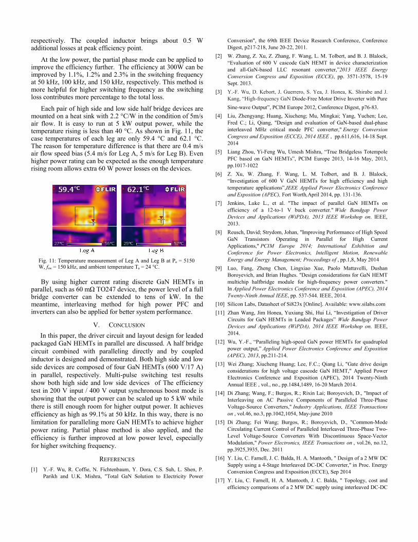
Fig. 11: Temperature measurement of Leg A and Leg B at Po = 5150 W, fsw = 150 kHz, and ambient temperature Ta = 24 °C.
respectively. The coupled inductor brings about 0.5 W additional losses at peak efficiency point.
At the low power, the partial phase mode can be applied to improve the efficiency further. The efficiency at 300W can be improved by 1.1%, 1.2% and 2.3% in the switching frequency at 50 kHz, 100 kHz, and 150 kHz, respectively. This method is more helpful for higher switching frequency as the switching loss contributes more percentage to the total loss.
Each pair of high side and low side half bridge devices are mounted on a heat sink with 2.2 °C/W in the condition of 5m/s air flow. It is easy to run at 5 kW output power, while the temperature rising is less than 40 °C. As shown in Fig. 11, the case temperatures of each leg are only 59.4 °C and 62.1 °C. The reason for temperature difference is that there are 0.4 m/s air flow speed bias (5.4 m/s for Leg A, 5 m/s for Leg B). Even higher power rating can be expected as the enough temperature rising room allows extra 60 W power losses on the devices.
By using higher current rating discrete GaN HEMTs in parallel, such as 60 mΩ TO247 device, the power level of a full bridge converter can be extended to tens of kW. In the meantime, interleaving method for high power PFC and inverters can also be applied for better system performance.
V. CONCLUSION In this paper, the driver circuit and layout design for leaded
packaged GaN HEMTs in parallel are discussed. A half bridge circuit combined with paralleling directly and by coupled inductor is designed and demonstrated. Both high side and low side devices are composed of four GaN HEMTs (600 V/17 A) in parallel, respectively. Multi-pulse switching test results show both high side and low side devices of The efficiency test in 200 V input / 400 V output synchronous boost mode is showing that the output power can be scaled up to 5 kW while there is still enough room for higher output power. It achieves efficiency as high as 99.1% at 50 kHz. In this way, there is no limitation for paralleling more GaN HEMTs to achieve higher power rating. Partial phase method is also applied, and the efficiency is further improved at low power level, especially for higher switching frequency.
REFERENCES [1] Y.-F. Wu, R. Coffie, N. Fichtenbaum, Y. Dora, C.S. Suh, L. Shen, P.
Parikh and U.K. Mishra, "Total GaN Solution to Electricity Power
Conversion", the 69th IEEE Device Research Conference, Conference Digest, p217-218, June 20-22, 2011.
[2] W. Zhang, Z. Xu, Z. Zhang, F. Wang, L. M. Tolbert, and B. J. Blalock, “Evaluation of 600 V cascode GaN HEMT in device characterization and all-GaN-based LLC resonant converter,”2013 IEEE Energy Conversion Congress and Exposition (ECCE), pp. 3571-3578, 15-19 Sept. 2013.
[3] Y.-F. Wu, D. Kebort, J. Guerrero, S. Yea, J. Honea, K. Shirabe and J. Kang, “High-frequency GaN Diode-Free Motor Drive Inverter with Pure Sine-wave Output”, PCIM Europe 2012, Conference Digest, p76-83.
[4] Liu, Zhengyang; Huang, Xiucheng; Mu, Mingkai; Yang, Yuchen; Lee, Fred C.; Li, Qiang, "Design and evaluation of GaN-based dual-phase interleaved MHz critical mode PFC converter," Energy Conversion Congress and Exposition (ECCE), 2014 IEEE , pp.611,616, 14-18 Sept. 2014
[5] Liang Zhou, Yi-Feng Wu, Umesh Mishra, “True Bridgeless Totempole PFC based on GaN HEMTs”, PCIM Europe 2013, 14-16 May, 2013, pp.1017-1022
[6] Z. Xu, W. Zhang, F. Wang, L. M. Tolbert, and B. J. Blalock, “Investigation of 600 V GaN HEMTs for high efficiency and high temperature applications”,IEEE Applied Power Electronics Conference and Exposition (APEC), Fort Worth,April 2014, pp. 131-136.
[7] Jenkins, Luke L., et al. "The impact of parallel GaN HEMTs on efficiency of a 12-to-1 V buck converter." Wide Bandgap Power Devices and Applications (WiPDA), 2013 IEEE Workshop on. IEEE, 2013.
[8] Reusch, David; Strydom, Johan, "Improving Performance of High Speed GaN Transistors Operating in Parallel for High Current Applications," PCIM Europe 2014; International Exhibition and Conference for Power Electronics, Intelligent Motion, Renewable Energy and Energy Management; Proceedings of , pp.1,8, May 2014
[9] Luo, Fang, Zheng Chen, Lingxiao Xue, Paolo Mattavelli, Dushan Boroyevich, and Brian Hughes. "Design considerations for GaN HEMT multichip halfbridge module for high-frequency power converters." In Applied Power Electronics Conference and Exposition (APEC), 2014 Twenty-Ninth Annual IEEE, pp. 537-544. IEEE, 2014.
[10] Silicon Labs, Datasheet of Si823x [Online]. Available: www.silabs.com [11] Zhan Wang, Jim Honea, Yuxiang Shi, Hui Li, “Investigation of Driver
Circuits for GaN HEMTs in Leaded Packages” Wide Bandgap Power Devices and Applications (WiPDA), 2014 IEEE Workshop on. IEEE, 2014.
[12] Wu, Y.-F., “Paralleling high-speed GaN power HEMTs for quadrupled power output,” Applied Power Electronics Conference and Exposition (APEC), 2013, pp.211-214.
[13] Wei Zhang; Xiucheng Huang; Lee, F.C.; Qiang Li, "Gate drive design considerations for high voltage cascode GaN HEMT," Applied Power Electronics Conference and Exposition (APEC), 2014 Twenty-Ninth Annual IEEE , vol., no., pp.1484,1489, 16-20 March 2014.
[14] Di Zhang; Wang, F.; Burgos, R.; Rixin Lai; Boroyevich, D., "Impact of Interleaving on AC Passive Components of Paralleled Three-Phase Voltage-Source Converters," Industry Applications, IEEE Transactions on , vol.46, no.3, pp.1042,1054, May-june 2010
[15] Di Zhang; Fei Wang; Burgos, R.; Boroyevich, D., "Common-Mode Circulating Current Control of Paralleled Interleaved Three-Phase Two-Level Voltage-Source Converters With Discontinuous Space-Vector Modulation," Power Electronics, IEEE Transactions on , vol.26, no.12, pp.3925,3935, Dec. 2011
[16] Y. Liu, C. Farnell, J. C. Balda, H. A. Mantooth, " Design of a 2 MW DC Supply using a 4-Stage Interleaved DC-DC Converter," in Proc. Energy Conversion Congress and Exposition (ECCE), Sep 2014
[17] Y. Liu, C. Farnell, H. A. Mantooth, J. C. Balda, " Topology, cost and efficiency comparisons of a 2 MW DC supply using interleaved DC-DC

converter," in Proc. IEEE International Symposium on Power Electronics for Distributed Generation Systems (PEDG), Jun 2014
[18] Waffler, S.; Kolar, J.W., "Efficiency optimization of an automotive multi-phase bi-directional DC-DC converter," Power Electronics and
Motion Control Conference, 2009. IPEMC '09. IEEE 6th International , vol., no., pp.566,572, 17-20 May 2009.