
parallel session – salon a (continues) - Ortra
39
1 SCIENTIFIC PROGRAM MONDAY, NOVEMBER 9, 2009 OPENING (SALON ABC) Session 1A1 COMCAS 2009 Plenary Session Chair: Shmuel Auster, Elta Systems Ltd., Israel Co-Chair: Barry Perlman, US Army CERDEC, United States 09:00-09:40 1A1-1 Welcome Addresses Shmuel Auster, Conference Chairman Barry Perlman, TPC Co-Chairman, MTT President Eli Opper, Chief Scientist, Israel Ministry of Industry, Trade and Labor John Vig, IEEE President Jozef Modelski, IEEE Region 8 Director Keynote Presentation: 1A1-2 Cognitive Radio Research and Commercialization: Challenges and Opportunities J. Mitola III, Keynote Speaker Stevens Institute of Technology, Hoboken, United States 09:40-10:10 Cognitive radio includes dynamic spectrum, reconfigurable wireless networks, and context- sensitive delivery of wireless services via often intermittent, heterogeneous radio networks. In this keynote address, Dr. Mitola will provide an overview of how cognitive radio is changing the demands placed on radio devices, subsystems, and network technologies in commercial, military, and public safety applications, including impact of the Nov 08 FCC Rule and Order (R&O). Keynote Presentation: 1A1-3 Gallium Nitride (GaN) Goes Mainstream: A Differentiated Semiconductor Technology in the RF Power Industry R. Van Buskirk RFMD, Greensboro, United States 10:10-10:40 This presentation will outline the current RF Power market and incumbent semiconductor technologies. The discussion will identify the breadth and depth of RF Power end market opportunities and will highlight current, high-profile defense and commercial applications. The attributes of Gallium Nitride (GaN) as the “right RF power semiconductor technology” at the “right time” will be discussed. 10:40-11:15 Coffee Break
Transcript of parallel session – salon a (continues) - Ortra

1
SCIENTIFIC PROGRAM
MONDAY, NOVEMBER 9, 2009
OPENING (SALON ABC) Session 1A1 COMCAS 2009 Plenary Session
Chair: Shmuel Auster, Elta Systems Ltd., Israel Co-Chair: Barry Perlman, US Army CERDEC, United States
09:00-09:40 1A1-1 Welcome Addresses Shmuel Auster, Conference Chairman Barry Perlman, TPC Co-Chairman, MTT President Eli Opper, Chief Scientist, Israel Ministry of Industry, Trade and Labor John Vig, IEEE President Jozef Modelski, IEEE Region 8 Director
Keynote Presentation: 1A1-2 Cognitive Radio Research and Commercialization: Challenges and Opportunities
J. Mitola III, Keynote Speaker Stevens Institute of Technology, Hoboken, United States
09:40-10:10
Cognitive radio includes dynamic spectrum, reconfigurable wireless networks, and context-sensitive delivery of wireless services via often intermittent, heterogeneous radio networks. In this keynote address, Dr. Mitola will provide an overview of how cognitive radio is changing the demands placed on radio devices, subsystems, and network technologies in commercial, military, and public safety applications, including impact of the Nov 08 FCC Rule and Order (R&O). Keynote Presentation: 1A1-3 Gallium Nitride (GaN) Goes Mainstream: A Differentiated Semiconductor Technology in the RF Power Industry
R. Van Buskirk RFMD, Greensboro, United States
10:10-10:40
This presentation will outline the current RF Power market and incumbent semiconductor technologies. The discussion will identify the breadth and depth of RF Power end market opportunities and will highlight current, high-profile defense and commercial applications. The attributes of Gallium Nitride (GaN) as the “right RF power semiconductor technology” at the “right time” will be discussed.
10:40-11:15 Coffee Break

2
MONDAY, NOVEMBER 9, 2009 (CONTINUES)
PARALLEL SESSIONS
PARALLEL SESSION – SALON A Session: 1D2 In Memory of Ben Munk: Metamaterials and Beamformers (Part 1)
Chair: Ruth Rotman, ELTA IAI, Israel Co-Chair: Amir Zaghloul, Virginia Tech, United States
1D2-1 The Legacy of Two Giants: In Memory of Ben Munk and Walter Rotman
R. Rotman Elta, Ashdod, Israel
11:15- 11:45
A paper in memory of the late, great Ben Munk, father of the Stealth and his views on metamaterials. 1D2-2 Realization of Rotman's Concepts of Beamformer Lenses and Artificial Dielectric Materials
A. I. Zaghloul1,2, O. Kilic3, S. J. Weiss1, E. D. Adler1
1US Army Research Laboratory, Adelphi, United States, 2Virginia Polytechnic Institute and State University, Falls Church, United States, 3The Catholic University of America, Washington, United States
11:45- 12:15
The paper addresses two concepts that were introduced by Walt Rotman and made major impacts in the areas of electromagnetic devices. The first which stands above all of Rotman’s innovations and has been named after him is Rotman Lens, which acts as a beamformer in electronically scanned arrays. The second is the artificial dielectric material, which has the potential of achieving constitutive parameters in the medium that are fundamentally different than the conventional dielectric materials.
12:15-14:00 Lunch
Session: 1A3 In Memory of Ben Munk: Metamaterials and Beamformers (Part 2)
Chair: Robert Mailloux, US Air Force Research Laboratory, United States Co-Chair: Moshe Tur, Tel-Aviv University, Israel
1A3-1 Subarray Technology for Time Delayed Scanning Arrays
R. J. Mailloux Air Force Research Laboratory, Hanscom AFB, United States
14:00- 14:30
Large phased arrays often require time delay in order to pass wide bandwidth waveforms. It is usually less expensive to enter the time delay at the subarray level, but this may increase the sidelobes due to array periodicity, called quantization lobes. This paper describes a number of techniques that are being used or proposed to eliminate these quantization lobes including randomizing subarray location or using overlapped subarrays. 1A3-2 Photonic TTD Beamforming M. Tur
Tel-Aviv University, Tel-Aviv, Israel 14:30- 15:00
Invited paper reviewing the state of Photonic Beamforming 1A3-3 A Complete Behavioral Model of Radiation-Pattern Characteristics of Phased Array Using a Novel Digital Phase Shifter
G. Coviello, G. Avitabile, F. Cannone Politecnico di Bari, Bari, Italy
15:00-15:30
A complete behavioral model for radiation-pattern characteristic of phased array joint to a novel phased array transmitter has been presented. The model has many input parameters and a lot of features, such as parametric simulations and unconventional two-dimensional color graph representation capability. It is an optimum instrument to investigate the performance of a beam-former. Measured values of three prototypes of the proposed architecture have been used to study the performances.
15:30- 15:50 Coffee Break

3
PARALLEL SESSION – SALON A (CONTINUES) Session: 1A4 Antennas for Wideband and Wireless Communications
Chair: Magdy Iskander, University of Hawaii, United States Co-Chair: Amir Boag, Tel-Aviv University, Israel
1A4-1 Antenna Arrays Technologies for Advanced Wireless Systems
M. F. Iskander, W. Kim, J. Bell, N. Celik, Z. Yun, H. Youn University of Hawaii, Honolulu, United States
15:50- 16:20
Phased array antennas have and will continue to be a critically important component in the development of future wireless systems. We will describe a novel phased antenna array design based on integrated ferroelectric material and Continuous Transfer Stub (CTS) phased array technology. Also, the development of an ultra wideband ground plane for phased antenna array systems will be discussed. 1A4-2 Omni Directional Ultra Wideband Biconical Antenna
I. Gronich Elta LTD., Ashdod, Israel
16:20 -16:40
The proposed antenna is a small ultra-wideband antenna that has an omni-directional pattern in the azimuth plane and two lobes which have a tilt of several degrees from the horizon in the elevation plane. 1A4-3 Compact Chip Monopole Antenna with Parasitic Patch for GPS Applications
J. Jung1, K. Kim1, J. Lee1, H. Lee2, Y. Lim1 1Chonnam National University, Gwang-ju, Republic of Korea, 2Dongkang college, Gwang-ju, Republic of Korea
16:40- 17:00
A chip monopole antenna with a parasitic patch is proposed for GPS applications. To reduce the dimensions of the antenna, the chip monopole antenna is composed of stacked meander, helix structures, and a parasitic patch. The impedance and radiation characteristics of the antenna are investigated. The measured results show that the proposed antenna, having compact dimensions of 3.6 × 5 × 1.3 mm, has a bandwidth of 60 MHz (1.53-1.59 GHz) and a maximum radiation gain of 0.53 dBi.
PARALLEL SESSION – SALON B Session: 1E2 Cell Planning Chair: Avi Freedman, Nice Systems, Israel
1E2-1 On Resource Allocation in Dense Femto-Deployments
J. Ling, D. Chizhik, R. Valenzeula Alcatel-Lucent, Holmdel, United States
11:15- 11:35
Femtocells offer a promising way of extending macrocellular network coverage to indoor residential environments. If femtocells are spaced one per home, each on it's own lot, interference is low. For dense deployments, i.e. multi-unit construction, SIRS can become very low. Thus we propose a greedy frequency planning algorithm which only uses measurements at the femto-access point. We report on the convergence, as well as the improvement in SIR due to using the new frequency plan 1E2-2 Measuring and Comparing Coverage Quality for Femtocell and Macrocell Broadband Data Services
J. A. Weitzen1,2, T. Grosch1 1Airvana, Chelmsford, United States, 2University of Massachusetts Lowell, Lowell, United States
11:35- 11:55
This paper presents the results of field tests to measure and compare indoor airlink data rates from femtocells to indoor coverage from macrocells and concludes that operators can expect to see significant improvement in average airlink data throughput relative to the existing macrocell network. Tests were conducted in a number of residences. This paper concentrates on UMTS/HSDPA measurements and presents the methodology used in the test program and offers summary results. 1E2-3 On the Necessity of Information Transmission Channel Characteristics Consideration in Wireless Systems Planning
P. N. Zakharov, A. F. Korolev, A. P. Sukhorukov, M.V. Lomonosov Moscow State University, Moscow, Russian Federation
11:55- 12:15
The errors, being a product of a common practice of using statistics of physical parameters of radio channel in network planning, instead of rigorous system-level parameters, are quantified analytically and experimentally. The obtained error values achieved 320% for local mean channel capacity and 3 orders for BER on significant part of analyzed spatial area, thus, the importance of information transmission channel characteristics use as a preferred metric in network planning is pointed out. 1E2-4 Special Facilities of Chirp Ionosonde
A. A. Kolchev, V. V. Shumaev, D. G. Shpak Mari State University, Yoshkar-Ola, Russian Federation
12:15- 12:35
Article describes some functional facilities in addition to building of oblique sounding ionograms. These methods permit to realize building of ionograms with specified delay time resolution and frequency resolution, separation signal and noise on exit of receiver, detection spectrum concentrate disturbance at receiving place and measuring characteristics of signal and noise, reconstruction of signal reflected from ionosphere, estimation ratio signal/noise in receiver band.
12:35-14:00 Lunch

4
MONDAY, NOVEMBER 9, 2009 (CONTINUES)
PARALLEL SESSION – SALON B (CONTINUES) Session: 1B3 Channel Modeling Chair: Avi Freedman, Nice Systems, Israel
1B3-1 Transmission Through Multiple Layers in UWB and Narrow Band Communications
A. Yahalom, Y. Pinhasi, E. Shifman, S. Petnev Ariel University Center of Samaria, Ariel, Israel
14:00- 14:20
In this work we will describe a model taking into account transmission through multiple layers which are a consequence of the inhomogeneity of the building materials our indoor environment is made of. Examples include hollow brick and plaster walls. Our model enables the analysis of a communication channel for both the narrow and wide band cases between adjacent rooms. Further more we compare our analysis with measurements performed in our laboratory and obtain adequate correspondence. 1B3-2 Applying Wavelet Transformation to RF System Modeling
B. J. Gerfault1, B. Godara2, M. Nau2
1Thales Communications, Cholet, France 2ISEP, Paris, France
14:20- 14:40
This paper describes a new approach to modeling RF systems using wavelet transformation. The inherent advantage of this new method is a simulation in both time domain and frequency domain at the same time: some blocks are modeled in the time domain and some models in the frequency domain. An application example is shown for the simulation of a wideband high-power amplifier. 1B3-3 The Influence of Antenna Directivity on Physical Layer Simulations of 802.11n Devices
D. Wittwer1, S. Azulay2, M. Elliott2, M. Martiskainen2, S. Krupa2
1Galtronics USA, Tempe, United States 2Galtronics Ltd., Tiberias, Israel
14:40- 15:00
The optimal antenna properties are being investigated for MIMO systems. Antenna directivity is often suggested to increase the link budget power. However, the impact of preferred directions on received multi-path signals is seldom considered. Here we improve upon existing channel models to include antenna directivity for physical layer simulations. The link budgets for 2x2 and (3 choose 2)x2 MIMO systems are presented using omni and directive antenna patterns 1B3-4 Deterministic Method of Information Transmission Channel Prediction in Multipath Environments
P. N. Zakharov, E. V. Mikhailov, A. F. Korolev, A. P. Sukhorukov, M.V. Lomonosov Moscow State University Faculty of Physics, Moscow, Russian Federation
15:00- 15:20
A general method for system-level channel characteristics prediction is proposed, based on site-specific propagation models, deterministic system models and spatial statistical generalization. Validation of the method implementation with direct measurements in a complex indoor environment demonstrated its high accuracy. The dependence of prediction accuracy upon spatial detailing of prediction has been investigated experimentally.
15:20- 15:50 Coffee Break

5
PARALLEL SESSION – SALON B (CONTINUES) Session: 1B4 Cell Optimization Chair: Arie Reichman, Ruppin Academic Center,
Israel 1B4-1 Fractional Frequency Reuse and Its Application to OFDMA
N. Chayat Alvarion Ltd., Tel-Aviv, Israel
15:50- 16:20
Planning techniques for Fractional Frequency Reuse are discussed. Use of FFR with modern OFDMA-based communication standards, such as 802.16 and LTE, will be illustrated. 1B4-2 Planning of WiMAX OFDMA Frame Parameters in Real World Deployments
A. Freedman1, Z. Nuss2 1Nice Systems Ltd., Petach-Tikva, Israel 2Alvarion Ltd., Tel-Aviv, Israel
16:20- 16:40
The WiMAX frame structure enables very high flexibility to various deployment scenarios, by fractional frequency re-use, time and frequency resource allocation per user adaptive modulation and coding etc. The article describes methods of planning of the various parameters of the WiMAX OFDMA frame in real deployment cases where the user density and propagation conditions are not uniform. The parameters to be designed include channel selection, segment, permutation base and others. 1B4-3 Green Cellular – A New Architecture for Minimal Emission from Mobile Phones
D. Ezri, S. Shilo Greenair Wireless, Ramat-Gan, Israel
16:40 – 17:00
In this talk we present a new architecture for cellular networks, aiming at minimal emission from mobile phones, without any additional radiation sources. The new architecture abandons the classical transceiver base station design and suggests the augmentation of transceiver base stations with receive only devices. We survey the technological implications of the architecture and present simulation studies and experiments proving its significant effect on exposure to mobile phone radiation. 1B4-4 A Perspective on Quality of Experience and Quality of Service Parameters in IPTV
M. Gershon Agilent Technologies, Petach Tikva, Israel
17:00- 17:20
This presentation will address the perceived quality of video services and the key challenges that impact IPTV performance. We will explain how to measure the many factors that influence IPTV Quality of Experience (QoE) in Triple Play networks including: * Quantification of the quality of streamed video and audio content; * Automated testing of channel zapping time; * Challenges of reliability. We discuss and assess techniques for evaluating the performance of IPTV and Triple Play devices.

6
MONDAY, NOVEMBER 9, 2009 (CONTINUES)
PARALLEL SESSION – SALON C Session: 1F2 Wave Propagation Chair: Gregory Samelsohn, Holon Institute of
Technology, Israel 1F2-1 Radio Propagation Modeling in Complex Environments for Wireless Communications
Z. Yun, S. Lim, M. F. Iskander University of Hawaii, Honolulu, United States
11:15- 11:45
In this paper, we will first review the ray-tracing algorithms developed in our group; then examples of the exploitation of geospatial data for radio propagation and its benefits will be presented. We will discuss the techniques to extract three dimensional (3D) building structures in urban propagation environment using 2D images in cyberspace. Finally, a real-time ray tracer will be briefly described. 1F2-2 The Predictability of Anomalous Propagation Environments
S. W. Marcus1, E. Tomer1, Y. Levi2 1Rafael, Haifa, Israel 2Israel Meteorological Service, Bet Dagan, Israel
11:45- 12:05
It is shown that anomalous propagation environments (ducts) can be predicted from meso-scale weather model data. The existence of surface-based atmospheric ducts was verified by the upward-tilted weather radar at Ben Gurion Airport which observed ships at locations well beyond the radar horizon. Once the duct parameters are known, their effects on the radar can be computed using available propagation models based on the parabolic approximation. 1F2-3 Asymptotic Analysis of Propagation Over Cluttered Parabolic Ridges
D. Chizhik, L. M. Drabeck, W. M. MacDonald Alcatel-Lucent, Holmdel, United States
12:05- 12:25
Analysis of radio propagation over varying, clutter-covered terrain was carried out from a transmitter placed above clutter to a terminal immersed in clutter. For parabolic ridges, ray-optical term dominated for short ranges, while a weak single mode dominated beyond the radio “horizon”, in contrast to strong focusing reported in valleys.
12:25-14:00 Lunch Session: 1C3 Radar and Electronic Systems I Chair: Stanley Rotman, Ben Gurion University,
Israel Co-Chair: R. W. McMillan, US Army Space and Missile Defense Command, United States
1C3-1 A Probabilistic Model of the Radar Signal-to-Clutter and Noise Ratio
R. W. McMillan1, I. Kohlberg2
1US Army Space and Missile Defense Command, Huntsville, United States, 2Kohlberg Associates, Inc., Reston, United States
14:00- 14:20
We consider the effects of atmospheric turbulence, target fluctuations based on the Swerling models, zero-mean Gaussian background and receiver noise, and lognormal-distributed clutter on radar performance. We combine these probabilistic effects to give the signal-to-clutter and noise ration (SCNR) as a function of normalized transmitted power. Results show that there is an optimum transmitted power level resulting in the best SCNR. 1C3-2 A 13.56 MHz Localization System Utilizing a Switched Injection Locked Transponder
T. Schaefer, F. Kirsch, M. Vossiek Clausthal University of Technology, Clausthal-Zellerfeld, Germany
14:20- 14:40
A low-frequency local positioning system at 13.56 MHz is presented. The system is aiming at short range indoor localization problems, where a measurement through a crowd of people is required. Ranging is accomplished by measuring the phase shift between a transmitted CW base station signal and the response from a transponder with the use of the novel switched injection locked oscillator concept. First measurement results prove that ranging with accuracy in the decimeter-range is possible. 1C3-3 Calibration Techniques for Digital Phased Arrays
C. J. Fulton, W. J. Chappell Purdue University, West Lafayette, United States
14:40- 15:00
Several techniques for calibrating and aligning different aspects of a digital phased array are demonstrated using a 16-element, panelized, vertically-polarized S-band subarray with element-level digitization on both transmit and receive. A method for maintaining element amplitude and phase over time in fully digitized arrays is demonstrated as well as a technique for element-level self-calibration of quadrature mismatches. 1C3-4 Doppler-Polarimetric Radar System for Recognition of Distributed Objects
F. J. Yanovsky National Aviation University, Kiev, Ukraine
15:00- 15:30
A concept of multifunctional Doppler-polarimetic radar system for distributed target investigation and recognition is developed. Phenomenological and statistical models are developed, experimental measurements are done and recognition algorithms are built and implemented. Theoretical and experimental results are compared.
15:30- 15:50 Coffee Break

7
PARALLEL SESSION – SALON C (CONTINUES) Session: 1C4 Radar and Electronic Systems II
Chair: Ruth Rotman, ELTA, Israel Co-Chair: Yossi Pinhasi, Ariel University Center of Samaria, Israel
1C4-1 Antenna and Beamformer Requirements for Wideband Phased Array Systems: A Review
R. Rotman, M. Tur Elta, Ashdod, Israel
15:50- 16:10
The paper will review the unique requirements for the antenna and beamformer in wideband imaging systems. 1C4-2 Improved Covariance Matrices for point Target Detection in Hyperspectral Data
Y. Sofer, E. Geva, S. R. Rotman Ben-Gurion University, Beer-Sheva, Israel
16:10- 16:30
Our goals in hyperspectral point target detection have been to develop a methodology for algorithm comparison and to advance point target detection algorithms through the fundamental understanding of spatial/spectral statistics. In this paper, we review our methodology as well as present new metrics. 1C4-3 Sub-millimeter Radar with Coherent Detection for Homeland Security Applications
Y. Pinhasi, B. Kapilevitch , R. Arusi, D. Hardon, B. Litvak, M. Anisimov Ariel University Center of Samaria, Ariel, Israel
16:30 – 16:50
Investigation, design and development of a sub-mmw remote sensing radar system for homeland security applications are presented. The radar, operating at 330GHz is based on transmission of a FMCW aimed at detection of concealed objects for ranges up to 20m. Distance measurements and preliminary THz imaging were made by performing data acquisition and signal processing commercial programs, resulting in a range resolution better than 1cm.
ROYAL H Ansoft Free Workshop (COMMERCIAL)
11:15-12:45 “Take the power of HFSS 12” HFSS version 12 introduction Antenna Wizard demonstration Ansoft Designer overview Optimizing array antenna design using co simulation with circuit and 3D EM solver

8
MONDAY, NOVEMBER 9, 2009 (CONTINUES)
PARALLEL SESSION – ROYAL H Session: 1D3 Millimeter-Wave RFICs
Chair: Danny Elad, IBM, Israel Co-Chair: Itzhak Shapir, ELTA Systems Ltd, Israel
1D3-1 60 GHz Components in CMOS for Low Power Compact Phase Array Applications
E. Cohen1,2, S. Ravid1, D. Ritter2
1Intel, Haifa, Israel 2Technion-Israel Institute of Technology, Haifa, Israel
14:00- 14:30
60GHz LNA/PAs, Phase shifters (PS), combiners and switches were designed for integrated phase array in CMOS. These components achieve best known power consumption and size compared to previous publication reported, thanks to the methodology flow and layout optimization that was created at 60 GHz. The extensive use of passive architecture together with the compact layout will enable full integrated phase arrays with tens of elements with 20mm2 size and less that 1 Watt of TX power. 1D3-2 Differential Output, Transformer Coupled Push-Push VCO and Divider for 60GHz Applications in 90nm CMOS
O. Degani, S. Ravid Intel Corporation, Haifa, Israel
14:30- 14:50
A push-push VCO with embedded transformers that provide differential outputs at oscillation frequency and second harmonic is presented. CML divider and buffers for divider output and 2nd harmonic output are also included. The measured VCO second harmonic output frequency is ~44.5-50[GHz] (~10.5%). The phase noise at 1[MHz] offset is ranging between -109 to -112[dBc/Hz] and -97 to -100 [dBc/Hz], for f0/2 and 2×f0 outputs, respectively. The supply is 1.3V supply and the circuit consumes ~20mA. 1D3-3 A Beyond 60GHz Cross-Coupled Fundamental VCO in 45nm CMOS
A. Katz1, O. Degani1, Y. Shacham2, E. Socher2
1Intel, Haifa, Israel, 2Tel-Aviv University, Tel-Aviv, Israel
14:50- 15:10
A beyond 60GHz cross-coupled NMOS differential LC CMOS VCO is presented in this paper, which is implemented in 45nm standard CMOS technology. Working with a supply voltage of 1.2V the circuit draws a current of 38mA and requires a circuit area of 0.037 mm square. The circuit delivers an output power of -9dBm to -11dBm and yields a measured phase noise of -102.2dBc/Hz at 10MHz offset. The VCO offers a frequency tuning range of 0.2GHz. 1D3-4 A Compact Low-Power 24 GHz Transceiver for Radar Applications in 0.13 um CMOS
V. Issakov1, M. Tiebout2, K. Mertens2, Y. Cao3, A. Thiede1, W. Simbuerger3, L. Maurer4 1University of Paderborn, Paderborn, Germany, 2Infineon Technologies Austria AG, Villach, Austria, 3Infineon Technologies AG, Neubiberg, Germany, 4DICE GmbH, Linz, Austria
15:10- 15:30
This paper presents a compact low-power transceiver for 24GHz radar applications integrated in 0.13um CMOS. The integration level includes an LNA, two mixers, on-chip quadrature generation, a VCO, a PA driver and division by four at a record minimal area of 0.7mm2. The receiver offers a conversion gain of 10dB and a NF of 7dB, whilst the transmitter provides an output power of -3 dBm and a phase noise of -102 dBc/Hz. The fully differential circuit consumes only 88mW from a single 1.5V supply.
15:30-15:50 Coffee Break
ROYAL H CST Free Workshops (COMMERCIAL)
15:50-17:20 Two CST free workshops: 1. "State of the art antenna design and placement on large platforms". 2. "Power Integrity Simulation for PCBs."

9
PARALLEL SESSION – ROYAL I Session: 1E3 EMC Materials and Models
Chair: Moshe Henig, RoadSensors Group, Israel Co-Chair: Saray Barakat, Israel Navy, Israel
1E3-1 Recent Developments in Radar Absorbing Paints and the Zinc Oxide Tetrapod Whisker
B. T. Caudle1, G. T. Flowers1, M. E. Baginski1, S. M. Wentworth1, S. M. Rao2
1Auburn University, United States 2US Naval Research Lab, Washington, United States
14:00- 14:20
Recent developments in the field of material science have revealed several new materials whose ElectroMagnetic (EM) properties make them ideal candidates for use as Radar Absorbing Materials (RAM). The new types of RAM materials can be applied as very thin layers of paint and still maintain their absorption effectiveness, making them ideal for Radar Cross Section (RCS) reduction. This article presents a brief review of the classes of RAM and an analysis of Zinc-Oxide tetrapod whiskers as RAM. 1E3-2 Equivalent Circuit for Parasitic Coupling Between Plated Through Holes within PCB Structures
L. Cornock, I. Dilworth University of Essex, Colchester, United Kingdom
14:20 14:40
We present an equivalent circuit for simulating parasitic coupling between adjacent plated through holes, known as vias, within multilayer printed circuit boards (PCB's) and similar structures. This paper uses full wave 3D electromagnetic models and measurement results as part of the development of the equivalent circuit. We also demonstrate how the modeling and perhaps the equivalent circuit presented can be scaled to fit virtually any via geometries including TSVs used in 3D IC packaging. 1E3-3 Accurate Modeling of Ferrite-Core Effects in Probes for Bulk Current Injection
F. Grassi Politecnico di Milano, Milano, Italy
14:40 15:00
The paper deals with circuit and electromagnetic modeling of injection probes for Bulk Current Injection in the SPICE and CST Microwave Studio environments. Different modeling strategies are used to assure accurate characterization of the frequency-dependent phenomena associated with the probe core. The proposed procedure resorts to preliminary probe input impedance measurements, and to Debye and Lorentian models for representing the core intrinsic and effective permeability spectra. 1E3-4 Insertion Loss of a Balanced Transmission Line Crossing Rectangular Apertures in dual Infinite Backplanes
S. W. Jung, K. C. Kim Yeugnam University, Gyeongsan-si, Republic of Korea
15:00- 15:20
This paper presents the backplane effects for a balanced transmission line crossing two rectangular apertures in dual infinite ground backplanes. The results show that the insertion gain is obtained from the half wavelength intervals for the total transmission line length. The backplane insertion loss and gain values vary depending on the length increase between dual conducting screens.
15:20- 15:50 Coffee Break

10
MONDAY, NOVEMBER 9, 2009 (CONTINUES)
PARALLEL SESSION – ROYAL I (CONTINUES) Session: 1E4 EMC Regulations and Non-Ionizing Radiation Hazards
Chair: Moshe Netzer, Rafael, Israel Co-Chair: Haim Mazar, Ministry of Communications, Israel
1E4-1 New Concept about Common Mode Noise
J. Tabasi Nejad Consultant, Toronto, Canada
15:50- 16:10
We will show that in a typical switch mode power supply (SMPS),3 types of conducted electromagnetic interference exist. This is a further development of the well known and widely applied theory that limits the type of noises to differential mode (DM) and common mode(CM).In this article, the 3 types of noise are categorized as: DM, single mode (SM) ground noise and CM ground noise. The new concept of the SM is useful in explaining how the symmetry can significantly reduce ground noise. 1E4-2 Report on a Cancer Cluster in an Antenna Ranges Facility
M. Peleg Rafael LTD., Haifa, Israel
16:10- 16:30
A cancer cluster comprising five workers diagnosed with cancer out of a group of about 30 occurred among young workers in an antenna ranges facility. The Odds Ratio (OR) was 8.3 with CI 95% of 2.3 to 19. No definite conclusions can be drawn from a single cluster, however together with other similar cases reported elsewhere it tends to indicate a severe cancer risk for young people exposed repetitively to non-ionizing radio-frequency radiation governed only by the ICNIRP thermal limits. 1E4-3 A Global Survey and Comparison of Different Regulatory Approaches to Non-Ionizing RADHAZ and Spurious Emissions
H. Mazar Ministry of Communications, Tel-Aviv, Israel
16:30- 16:50
A survey of regulations and standards in 235 countries worldwide reveals different approaches associated with RADHAZ and spurious emissions. These are primarily divided into regions regulated or influenced by Europe or by North America, each applying different limits to cellular base stations, utility power lines and spurious emissions. Generally, the American and Japanese permitted exposures are more lenient, whereas the European are stricter. Several interesting examples are discussed.

11
PARALLEL SESSION – ROYAL J Session: 1F3 Computational Methods in Electromagnetics
Chair: Reuven Shavit, Ben-Gurion University, Israel
1F3-1 Metamaterials and Their Applications
S. W. Marcus, C. Schwartz, M. Naor Rafael, Haifa, Israel
14:00- 14:30
The macroscopic behavior of materials in an EM field is determined by their values of permittivity and permeability which are generally positive. It has been found possible, however, to engineer materials for which these parameters are effectively negative. Such 'negative' materials are referred to as metamaterials. The effect of metamaterials on phase velocity, refraction, scattering and transmission will be discussed, as well as their applications to lenses and cloaks. 1F3-2 Shielding Properties of Conductive Concrete Against Transient Electromagnetic Disturbances
A. Ogunsola1, U. Reggiani2, L. Sandrolini2 1Parsons Group International, London, United Kingdom, 2University of Bologna, Bologna, Italy
14:30-14:50
This paper studies the shielding properties of conductive concrete exposed to a transient electromagnetic pulse. The conductive concrete is a cementious composite having a low volume concentration of steel fibers. It is shown that the real and imaginary parts of the complex relative permittivity of the composite are higher than those of an undoped concrete. For the case investigated their increases do not translate into significant augmentation of the shielding effectiveness of the composite. 1F3-3 Modeling Bond Wires for Millimeter Wave RFIC Design
S. Hauptmann, M. Hellfeld, C. Knochenhauer, F. Ellinger TU Dresden, Dresden, Germany
14:50- 15:10
This paper discusses how bond wires can be accurately modeled for circuits operating at several 10 GHz. To obtain exact results a more sophisticated model than the commonly-used inductor with around 0.8 nH/mm is required. An edge-based multiple conductor transmission line (mtline) model is presented, and it is demonstrated how its parameters can be extracted from EM simulations. A comparison of the mtline model with a lumped components model demonstrates the advantages of the mtline approach. 1F3-4 The Use of 3D Electromagnetic Simulation Tools in the Design of Microwave Integrated Circuits: An Accuracy Assessment
R. S. Tomar1, P. Pramanick2, P. Bhartia3 1The LNM Institute of Information Technology, Jaipur, India, 2M2 Global Inc., San Antonio, United States, 3NATEL Engineering Co., Inc., Chatsworth, United States
15:10- 15:30
The accuracy of Ansoft's 3-dimensional electromagnetic (3d EM) simulation tools in predicting real-life performance of radio frequency (RF) and Microwave circuits is assessed through investigating several original design examples. Generally speaking, the High Frequency Structure Simulator (HFSS) tool displays much higher accuracy compared to the accuracy displayed by the Circuit Simulator tool.
15:30- 15:50 Coffee Break

12
MONDAY, NOVEMBER 9, 2009 (CONTINUES)
PARALLEL SESSION – ROYAL J (CONTINUES) Session: 1F4 Terahertz Technology and Applications
Chair: Amir Abramovich Co-Chair: Boris Kapilevich Ariel University Center of Samaria, Israel
1F4-1 Single Pixel THz Detector for Remote Imaging
B. Kapilevich, Y. Pinhasi, M. Anisimov, R. Arosi, B. Litvak, D. Hardon The Ariel University Center of Samaria, Ariel, Israel
15:50- 16:10
High-resolution single-pixel detector operating near 0.33 THz is described. It consists of FMCW transmitter based on multiplying chain (x32) and heterodyne receiver with sub-harmonic mixer. The X-band FMCW synthesizer is employed as a driver of multiplying chain and LO of the mixer. The Gaussian-beam antennas are used in the Rx and Tx channels. The detector was mounted on the scanning platform and can be employed in various homeland security applications needed the remote detection. 1F4-2 Terahertz Resonant Frequencies of Grating-Bicoupled Plasma Wave Devices
D. Khmyrova University of Aizu, Aizu-Wakamatsu, Japan
16:10- 16:30
Paper deals with the evaluation of resonant frequencies of plasma oscillations in the grating-bicoupled HEMT-like structure. Analytical model is developed. Resonant modes are calculated in the presence of non-saturated source-drain current for different combinations of gate bias voltages. 1F4-3 THz Imaging using Inexpensive Glow Discharge Detector Pixels
N. S. Kopeika1, A. Abramovich2, H. Joseph1, A. Akram2, O. Yadid-Pecht1, A. Belenky1, S. Lineykin1
1Ben-Gurion University, Beer-Sheva, Israel 2The Ariel University Center of Samaria, Ariel, Israel
16:30- 16:50
The properties of terahertz (THz) radiation are well known. They penetrate well most non-conducting media; there are no known biological hazards, and atmospheric attenuation is lower than for visual and IR radiation. Recently we have found that common miniature commercial neon glow discharge detector (GDD) lamps costing typically about 30 cents each exhibit high sensitivity to THz radiation, with microsecond order rise times, thus making them excellent candidates for such focal plane arrays. 1F4-4 CMOS-SOI-MEMS Transistor (TeraMOS) for Terahertz Imaging
D. Corcos2, D. Goren1, Y. Nemirovsky2
1IBM – Haifa Research Laboratories, Haifa, Israel, 2Technion – Israel Institute of Technology, Haifa, Israel
16:50- 17:10
This study presents a new sensor for Terahertz imaging which is based on several leading technologies: CMOS-SOI, MEMS and Terahertz Photonics. The paper focuses on the electrical characterization of "virgin" (unreleased) transistors fabricated in the IBM 0.18um process. By applying MEMS post processing, the now thermally isolated transistors become highly sensitive "active bolometers"-the TeraMOS sensors. The Temperature Coefficient of Current (TCC) and a new figure of merit are presented. 1F4-5 Attenuated Total Reflectance (ATR)-FTIR Spectral Measurements in MIR and FIR (THz) Range
A. Abramovich, A. Shulzinger Ariel University Center of Samaria, Ariel, Israel
17:10- 17:30
Mid-Infrared (MIR) spectroscopy is an extremely reliable and well recognized fingerprinting method. Far-Infrared (THz) spectroscopy has unique properties for fingerprinting. The technique of Attenuated Total Reflectance (ATR) has in recent years revolutionized solids, powders and liquid sample analyses because it combats the most challenging aspects of infrared analyses, namely sample preparation and spectral reproducibility. Characterization of materials using ATR in MIR and FIR is presented.

13
PARALLEL SESSION 1G – FOYER Session: 1G3 Poster Session I
1G3-1 Planning of Truncated Sequential Binomial Tests via the ASN-increase Parameter
Y. Michlin1, O. Shaham2
1Technion-Israel Institute of Technology, Haifa, Israel, 2Rafael, Haifa, Israel
The binomial Sequential Probability Ratio Test is the most common acceptance test of electronic systems. Goal: a planning methodology and tools for such a test. Presents parameters for assessment of the quality of a planned test. One of these parameters is the increase in the average sample number caused by the truncation. An optimality criterion based on it considerably facilitates solution. Also given are formulas for determining of the Truncation Apex. A user's algorithm is also included. 1G3-2 Dual Frequency Cavity Resonator for Atomic Manipulation and Spectroscopy
I. Gurman, Y. Soreq, R. Shavit, M. Givon, D. Groswasser, G. Aviv, R. Fulman
Ben-Gurion University, Beer-Sheva, Israel We propose a new approach for the design of a cavity for atom vapor based devices, where atomic manipulation via two frequencies is required. The cavity provides a homogenous field at two different frequency bands – 6.8GHz and 2MHz; the first frequency is supported by a cylindrical resonator with conductive walls and dielectric bases, the second frequency is applied from an external source and penetrates into the cavity resonator thin metal walls. 1G3-3 Wideband receiver-module for 3 mm wave focal plane imaging array
V. B. Khaikin1, V. N. Radzikhovsky2, S. E. Kuzmin3, V. R. Zakamov3
1The Special Astrophysical Observatory, RAS, St. Petersburg, Russian Federation, 2Institute of Electronics and Communication, Kiev, Ukraine 3Institute of Electronics and Communication, Kiev, Ukraine
Results of calculation and optimization of symmetrical and offset Cassegrain antennas with a tight multibeam focal plane array for MM wave imaging are given. A wideband compact receiver module of 3 mm band for a focal plane imaging array has been developed on the basis of InP MMIC LNA and a high sensitive impedance matched low-barrier detector diode. The gain factor not less than 30 dB was achieved at 85…97 GHz. Measured temperature sensitivity of the receiver module is 20 mK/Hz1/2. 1G3-4 Time Reversal of Electromagnetic Waves in Random Channels with Anisotropic Disorder
G. Samelsohn, E. Gruzdev Holon Institute of Technology, Holon, Israel
Time reversal (TR) is a powerful technique allowing for both space focusing and time compression of (ultra-)wideband signals. In the present work, we investigate time reversal and the phenomena of wave transport (localization, diffusion, etc.) for anisotropically disordered structures. The results obtained show that the resolution of time reversal, i.e., the ability of the system to refocus the wave in both space and time, depends essentially on the material anisotropy and propagation angle. 1G3-5 Multifunctional Microwave Devices Based on Metamaterial Transmission Lines
I. Vendik, D. Kholodnyak, P. Kapitanova, K. Zemlyakov Electrotechnical University, St. Petersburg, Russian Federation
One-dimensional metamaterial realized as cascaded transmission lines with positive and negative dispersion is used for a design of multifunctional microwave devices: multi-mode planar resonators with arbitrary resonant frequencies, multi-band tuneable filters, tuneable and reconfigurable directional couplers. Results of simulations and experimental investigations are presented and discussed. 1G3-6 Impedance Matching Using 3 Parasitic Elements
L. Felman, A. Sofer, H. Matzner Holon Institute of Technology, Holon, Israel
09:30- 15:30
A microstrip circuit is matched by using three parasitic elements, where by "parasitic" we mean that there is no physical connection between the matching elements and the main circuit. A 1:2 microstrip divider is used as an example, for which three parasitic elements are located on the strips of the divider. The divider was simulated and measured, showing a very good level of matching quality. Very good agreement between simulation and measurement was achieved.

14
MONDAY, NOVEMBER 9, 2009 (CONTINUES)
PARALLEL SESSION 1G – FOYER (CONTINUES) Session: 1G3 Poster Session I (continues)
1G3-7 Design and Analysis of Bandstop Filter Using E-Shaped Dual Mode Resonator
S. Saxena1, S. Porwal1, K. Soni1, P. Chhawchharia1, S. K. Koul2 1Geetanjali Institute of Technical Studies, Udaipur, India, 2Indian Institute of Technology, New Delhi, India
Design and Analysis of Bandstop Filter using E – Shaped Dual Mode Resonator is reported. Simulation shows a rejection level of -16.2 dB at centre frequency of 6 GHz. Experimental tests with VNA resulted in centre frequency of 6.3 GHz with rejection level of -17.814 dB. Novel design with mirror imaging of resonator showed a rejection level of -32 dB. The fractional bandwidth of 646 MHz with return loss -2.3 dB were obtained. Detailed analysis is reported. 1G3-8 A Novel Tunable Bandstop Filter Using E–Shaped Dual Mode Resonator
S. Saxena1, S. Porwal1, K. Soni1, P. Chhawchharia1, S. K. Koul2 1Geetanjali Institute of Technical Studies, Udaipur, India, 2Indian Institute of Technology, New Delhi, India
Novel Tunable Bandstop Filter using E–Shaped Dual Mode Resonator is reported. Variation in frequency is achieved by changing centre stub length Lc. With Lc=10mm centre frequency of 4.974 GHz and rejection level of -17dB is achieved. Effect of DC bias and PIN diode network on tunability is analyzed. Simulation results show frequency of 5.23 GHz with rejection level of -20.907dB in forward bias and 5.982 GHz with rejection level of -21.907dB in reverse bias. Tunability of 752 MHz is achieved. 1G3-9 MEMS Tunable Capacitor with Wide Tuning Range Using Multiple Voltage Sources
O. Lavy, L. Gal, D. Weicherman, S. Stolyarova, E. David, A. Saad, Y. Nemirovsky Technion-Israel Institute of Technology, Haifa, Israel
This paper presents a MEMS surface micr-machined varactor. The dynamic range of this class of varactors is governed by pull-in instability which is ideally one third of the initial gap between the two electrodes. This paper presents a simple T varactor, whose pull-in stability and hence its dynamic range is increased by applying two independent voltage sources. We introduce an electromechanical model for the proposed structure, and a full analytic solution to the attached pull-in problem 1G3-10 Assessment of Optimal Exposure Time of Broadband Microwave Radiation on Bone Marrow Cell Vitality
V. E. Dobrova, E. V. Dolzhikova, L. M. Maloshtan, E. A. Stepanova National University of Pharmacy, Kharkov, Ukraine
In this study, we investigated the effect of exposure time of broadband microwave radiation on bone marrow cell cultures. The cells were illuminated using a broadband noise source in the range from 60 to 400 GHz. The vitality of the cells was estimated as a proportion of dead cells. All experimental results were treated employing statistical methods. The optimal exposure time was determined for specific experimental conditions. The cytoprotective influence of mm-wave radiation was assessed. 1G3-11 High Resolution High Power W-Band Spectroscopy System (92-100 GHz)
E. Gross, A. Abramovich, C. Bruma, E. Farber Ariel University Center of Samaria, Ariel, Israel
09:30- 15:30
High resolution high power W-band (92-100 GHz) spectroscopic system was constructed and experimentally tested. The system is based upon two parabolic mirrors, high power high resolution CW (continuous wave) tunable THz source and unique THz detector. The spectrometer is fully computerized. Spectral resolution of Tens of kHz is achievable. The system was designed to measure transmission function of sample using wide collimated beam of 75 mm diameter in order to simulate THz imaging situation.

15
TUESDAY, NOVEMBER 10, 2009
PARALLEL SESSIONS
PARALLEL SESSION – SALON A Session: 2A1 Wideband Antennas and Arrays Chair: Reuven Shavit, Ben Gurion University,
Israel 2A1-1 An Efficient Decoupling Feeding Network for Phased Arrays
E. Rivkin, R. Shavit Ben-Gurion University, Beer-Sheva, Israel
09:00-09:30
A new approach is proposed for designing a decoupling feeding network for phased arrays. The proposed approach results in significant hardware savings and enables to match each of the input ports individually and independently of the excitation. 2A1-2 Overview of GPS Antennas E. Levine
AFEKA College of Engineering, Tel-Aviv, Israel 09:30-09:50
GPS are gaining large ampunt of attention in recent years. The key factor for the positioning accuracy and for short acquisition time is the antenna. It is the objective of this paper to present the requirements from GPS antennas and to describe and compare different types of antennas. 2A1-3 Compact Printed Semicircular Patch Microstrip Line Fed Monopole Antennas for UWB Applications
R. Pillalamarri1, S. R. Gottapu2, S. K. S 3 1JNT University, Kakinada, India 2Andhra University, Visakhapatnam, India 3JNT University, Kakinada, India
09:50-10:10
In this paper we have investigated compact printed semicircular disc monopole antenna, which is basically printed microstrip antenna with etched ground plane for UWB applications. In particular we have simulated very compact semicircular disc monopole antennas for UWB communication. Simple rectangular microstrip line is used for feeding the printed monopole antenna and its frequency bandwidth under -10dB return loss is ranging from 3GHz to 11.6 GHz. 2A1-4 Novel Printed Planar Circular Patch Monopole Antennas for UWB Operations
R. Pillalamarri1, S. R. Gottapu2, S. K. S3
1JNT University, Kakinada, India 2Andhra University, Visakhapatnam, India 3JNT University, Kakinada, India
10:10-10:30
We have investigated printed Circular disc monopole antenna in this summary/paper, which is basically printed microstrip antenna with etched ground plane for UWB applications. In particular we have simulated circular disc monopole antenna with etched ground plane. Simple rectangular microstrip line is used for feeding the printed monopole antenna and which is having impedance of 50 Ohms. This designed circular disc UWB monopole antenna works well for the whole UWB frequency band 3.1-10.6GHz.
10:30-11:15 Coffee Break

16
TUESDAY, NOVEMBER 10, 2009 (CONTINUES)
PARALLEL SESSION – SALON A (CONTINUES) Session: 2A2 Novel Antenna Techniques and Advanced Manufacturing
Chair: Ely Levine, Afeka College, Israel
2A2-1 Advanced Antenna Manufacturing Technologies
S. Krupa1, D. Wittwer2, M. Martiskainen1, M. Elliott1, D. Lee3, S. Harel1, Y. Shalgi1, S. Quantz4
1Galtronics, Ltd., Tiberias, Israel, 2Galtronics, USA, Tempe, United States, 3Galtronics Korea, Gunpo-city, Democratic People's Republic of Korea, 4Galtronics Electronics (Wuxi) Co., Wuxi New High Technical & Development Zone, China
11:15-11:45
Advanced antenna manufacturing processes can help antenna engineers meet or exceed the stringent performance and packaging needs (both present and future) for several disparate consumer wireless markets/ product categories. This presentation details our unique, proprietary execution of the following advanced manufacturing processes: In-Mold Labeling (IML), Print-and-Plate conductor deposition, and High Performance/ Low Cost RF Substrate Assemblies. 2A2-2 Reduction of Mutual Coupling Between Antennas by Near-Field Coupled Resonators
A. Boag1, A. Boag2 1IDF, Tel-Aviv, Israel 2Tel-Aviv University, Tel-Aviv, Israel
11:45-12:05
In this work, we examine a configuration comprising three antennas, viz., a transmitting aggressor, a receiving victim, and a parasitic resonant element. The parasitic element is strongly excited by the aggressor’s radiation at frequencies close to its self resonance. This resonant element is designed to cancel the radiation from the aggressor at the location of the victim through strong near fields thanks to its close proximity to the victim.
12:05-12:25 2A2-3 Low Cost Ferroelectric Phase Shifter for a Higher Microwave Power Level
O. Vendik1, A. Vasiliev1, M. Parnes2 1Electrotechnical University, St. Petersburg, Russian Federation, 2Resonance. Ltd., St. Petersburg , Russian Federation
New requirements are formulated for phase shifters used in phased-array antennas: 1) small power in biasing networks, 2) higher microwave power, 3) low production cost. Reflection type phase shifters on ferroelectric tunable capacitors in combination with hybrid junction form a transmission type phase shifter. Two ferroelectric capacitors are connected in parallel with respect to RF voltage and in series with respect to dc bias. Such a scheme provides 10 W for each reflection type phase shifter. 2A2-4 VHF Multi Channel Coupler for RF Communication
E. Glassner, M. Mizrachi, E. Farber, N. Bachar, A. Abramovich, Y. Kor-Al Ariel University Center of Samaria, Ariel, Israel
12:25-12:45
The transmission of several channels via a single antenna is a long standing problem. This system of phase shifters, based on hybrid coupler and capacitors bank, are installed on each channel. Matching of the full system is done by choosing the capacitor value of each channel and is automatically done by the control unit.
12:45-14:00 Lunch

17
PARALLEL SESSION – SALON A (CONTINUES) Session: 2A3 Antenna Technology: Theory and Analysis I
Chair: Haim Metzner, Holon Institute of Technology, Israel
2A3-1 A Novel Semi-Analytic Method for 3D Scattering Problems
A. M. Serebrennikov Mining Institute of Ural Branch of Russian Academy of Sciences, Perm, Russian Federation
14:00-14:30
The method for the solution of scattering problems with homogeneous dielectric scatterers based on a single coordinate multipole expansion is proposed. Its convergence is proved. The sources of ill-conditionality of the constitutive algebraic system are established. The method of its regularization is suggested. The method of discrete drains is being proposed, as a method for checking the accuracy of the multipole approximation. The numerical analysis is performed for different testing objects. 2A3-2 A Wideband Flat Spiral Antenna with Planar Unbalanced Feed
N. Kimiagarov, H. Matzner, Holon Institute of Technology, Holon, Israel
14:30-14:50
A high gain 3-arm spiral antenna with planar unbalanced feed is proposed. It is shown that the traditional characteristic of spiral antenna apply to this type of spiral antenna. A very wide band frequency range and circularly polarization are achieved. Very good agreement between simulation and measurement was achieved, showing about f: 8f bandwidth, 8dBi gain. 2A3-3 A Printed Dual Dipole Antenna with Modified Ground Plan
H. Lee1, J. Jung2, Y. Seo2, J. An2, Y. Lim2 1Dongkang College, Gwang-ju, Republic of Korea, 2Chonnam National University, Gwang-ju, Republic of Korea
14:50-15:10
This paper proposes a printed dual dipole antenna for WLAN and DSRC. The proposed dipole antenna of a dual couple arm, which consists of two dipole strips, has a modified dual monopole and modified strips by the ground plan. Prototypes of the proposed antenna designed for WLAN operations in 5 GHz (5.15~5.825 GHz) bands and DSRC operations in 5.8GHz (5.795~5.875GHz) have been constructed and tested. The simulation peak gain is 2.8 dBi at 5.32 GHz. 2A3-4 Planar Antenna for a Cellular Phone
M. Martiskainen, M. Elliott, D. Wittwer, S. Azulay, S. Krupa Galtronics Corporation Ltd., Tiberias, Israel
15:10-15:30
This paper provides a solution for a multi-band antenna solution that can be fully integrated on the PCB of the device. The design is based on the concept that the primary function of the antenna elements in a mobile phone is to “illuminate” the chassis of the device. The chassis then becomes the main radiator. These antenna elements can be printed on PCB board with dimensions that are compatible with real estate available in mobile phones. This paper looks to the performance in free space.
15:30-15:50 Coffee Break
18
TUESDAY, NOVEMBER 10, 2009 (CONTINUES)
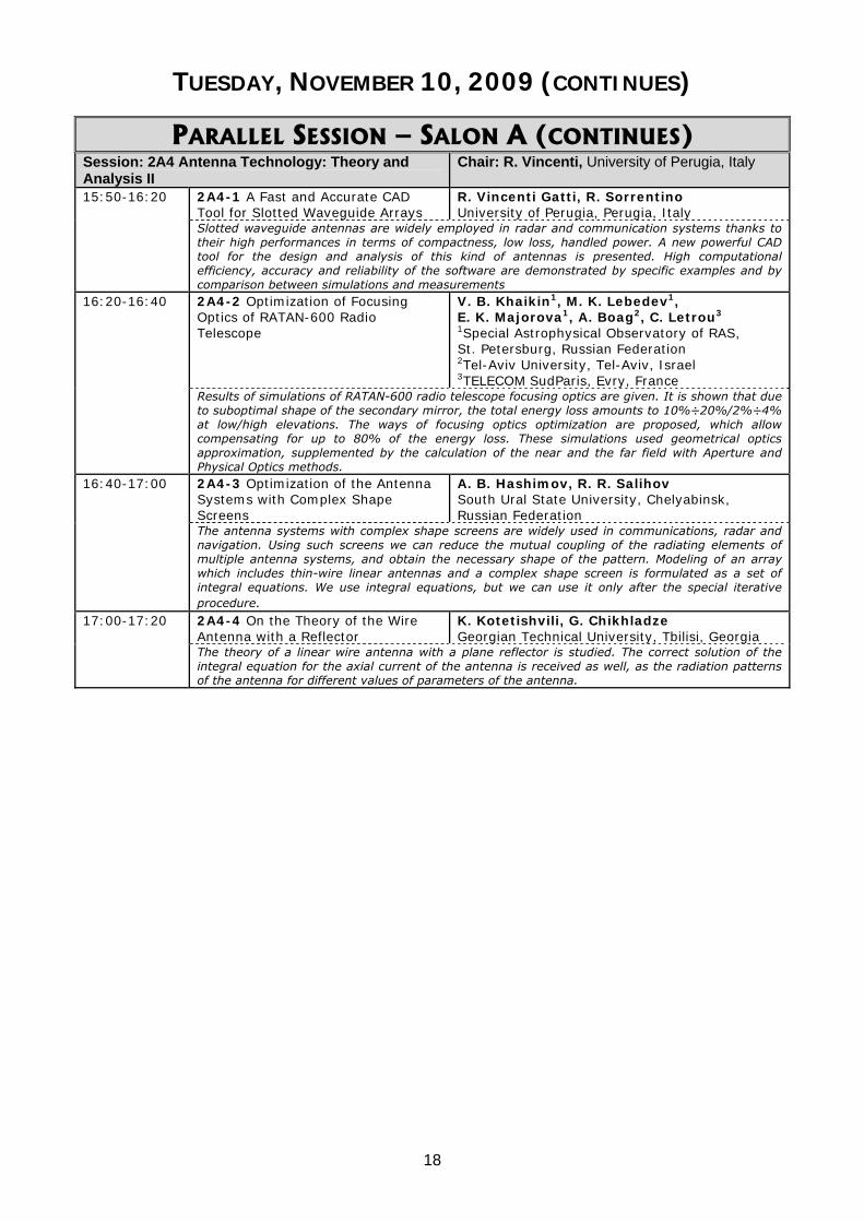
PARALLEL SESSION – SALON A (CONTINUES) Session: 2A4 Antenna Technology: Theory and Analysis II
Chair: R. Vincenti, University of Perugia, Italy
2A4-1 A Fast and Accurate CAD Tool for Slotted Waveguide Arrays
R. Vincenti Gatti, R. Sorrentino University of Perugia, Perugia, Italy
15:50-16:20
Slotted waveguide antennas are widely employed in radar and communication systems thanks to their high performances in terms of compactness, low loss, handled power. A new powerful CAD tool for the design and analysis of this kind of antennas is presented. High computational efficiency, accuracy and reliability of the software are demonstrated by specific examples and by comparison between simulations and measurements 2A4-2 Optimization of Focusing Optics of RATAN-600 Radio Telescope
V. B. Khaikin1, M. K. Lebedev1, E. K. Majorova1, A. Boag2, C. Letrou3
1Special Astrophysical Observatory of RAS, St. Petersburg, Russian Federation 2Tel-Aviv University, Tel-Aviv, Israel 3TELECOM SudParis, Evry, France
16:20-16:40
Results of simulations of RATAN-600 radio telescope focusing optics are given. It is shown that due to suboptimal shape of the secondary mirror, the total energy loss amounts to 10%÷20%/2%÷4% at low/high elevations. The ways of focusing optics optimization are proposed, which allow compensating for up to 80% of the energy loss. These simulations used geometrical optics approximation, supplemented by the calculation of the near and the far field with Aperture and Physical Optics methods. 2A4-3 Optimization of the Antenna Systems with Complex Shape Screens
A. B. Hashimov, R. R. Salihov South Ural State University, Chelyabinsk, Russian Federation
16:40-17:00
The antenna systems with complex shape screens are widely used in communications, radar and navigation. Using such screens we can reduce the mutual coupling of the radiating elements of multiple antenna systems, and obtain the necessary shape of the pattern. Modeling of an array which includes thin-wire linear antennas and a complex shape screen is formulated as a set of integral equations. We use integral equations, but we can use it only after the special iterative procedure. 2A4-4 On the Theory of the Wire Antenna with a Reflector
K. Kotetishvili, G. Chikhladze Georgian Technical University, Tbilisi, Georgia
17:00-17:20
The theory of a linear wire antenna with a plane reflector is studied. The correct solution of the integral equation for the axial current of the antenna is received as well, as the radiation patterns of the antenna for different values of parameters of the antenna.

19
PARALLEL SESSION – SALON B Session: 2B1 Adaptive Coding and Modulation Chair: Naftali Chayat, Alvarion, Israel
Co-Chair: Newton Love, Interactive Technology Solutions, United States
2B1-1 On Increasing Spectral Efficiency of Frequency Division Multiple Access Using Synchronized Superposition Modulation
D. Wulich1, G. R. Tsouri2, R. Dabora1 1Ben-Gurion University, Beer-Sheva , Israel 2Rochester Institute of Technology, Rochester, United States
09:15-09:35
We investigate the use of synchronized superposition-modulation for increasing spectral efficiency of frequency division multiple access systems such as the long-term evolution of UMTS. We present the basic concept and depict results for an arbitrary two-user scenario. A method of optimizing constellations for multiple users is presented based on maximizing the sum-rate mutual-information. The optimization method is applied to a three-user scenario. 2B1-2 Performance Comparison between Hermitian Codes and Shortened Non-binary BCH Codes
M. Jibril, M. Tomlinson, M. Z. Ahmed, C. Tjhai University of Plymouth, Plymouth, United Kingdom
09:35-09:55
We explore the benefits of implementing Hermitian codes and compare decoding performance in the additive white Gaussian noise (AWGN) channel and performance in the erasure channel of Hermitian codes with shortened non-binary Bose Hocquenghem Chaudhuri (BCH) codes. We implement the Berlekamp-Massey-Sakata (BMSA) decoding and Berlekamp-Massey (BMA) decoding for the hard decision Hermitian and BCH codes respectively, erasure decoding and ordered reliability soft decision decoding for both. 2B1-3 A Distance-Bounding Concept for Bilateral IEEE 802.15.4 Communication
J. Wittwer, F. Kirsch, M. Vossiek Clausthal University of Technology, Clausthal-Zellerfeld, Germany
09:55-10:15
The paper introduces a concept for bounding the operation range of IEEE 802.15.4 wireless sensors. The distance bounding is based on round-trip time-of-flight measurement. Based on a Wiener optimal filter for the packet preamble the time of arrival is determined. Precise clock synchronization is achieved by evaluating the instantaneous frequency of the received signal. Measurements prove that the introduced concept provides a distance-bounding accuracy of approx. 1 m even in indoor environments.
10:15-11:15 Coffee Break

20
TUESDAY, NOVEMBER 10, 2009 (CONTINUES)
PARALLEL SESSION – SALON B (CONTINUES) Session: 2B2 Transmitter and Receiver Modulation Techniques
Chair: Naftali Chayat, Alvarion, Israel Co-Chair: Newton Love, Interactive Technology Solutions, United States
2B2-1 A New Architecture for Coherent M-PSK Receivers
Y. Linn Universidad Pontificia Bolivariana, Bucaramanga, Colombia
11:15-11:35
In this paper we present a new architecture for coherent M-PSK receivers. This architecture has several unique characteristics: (a) it is very suitable for compact implementation within an FPGA or an ASIC; (b) it is resilient to AGC imperfections; (c) it is particularly optimized for implementation using fixed-point binary arithmetic. Thus, the proposed architecture is ideal for use in low-power, high-datarate wireless communications systems. 2B2-2 Optimization of the Carrier Tracking Loop for 8PSK Transmission
S. Landis, B. Bobrovsky Tel-Aviv University, Tel-Aviv, Israel
11:35-11:55
The performance of discrete-time Decision Directed (DD) first order Phase Looked Loops (PLL) for a 8PSK modulated signal is evaluated under the disturbance of thermal noise and $1/f^2$ phase noise. Fokker-Planck techniques are applied to compute the Mean Time to Lose Lock for both PLLs. We optimize the loop filter using the MTLL as the optimization criterion. Results are applied to investigate the necessity of pilots for 8PSK reception in DVB-S2. 2B2-3 Power Spectral Analysis of Spectral Shaping Trellis Coded Modulation
J. Park1, S. B. Gelfand1, M. P. Fitz2 1Purdue University, West Lafayette, United States, 2Northrop Grumman Corporation, El Sequndo, United States
11:55-12:15
A nonlinear binary code with a single carrier M-QAM linear modulation is designed to control certain transitions in the symbol constellation. This concept is employed to develop spectral shaping modulation codes with M-QAM linear modulations so as to reduce out-of-band power. The code is realized as a nonlinear binary convolutional code, and the coded modulation is represented as a Markov chain. The closed form of the power spectral density for this trellis coded modulation is derived. 2B2-4 Joint Optimization of Data Predistortion and Baseband Pulse Shaping in High Speed Transmission Nonlinear Systems
J. Park1, S. B. Gelfand1, M. P. Fitz2 1Purdue University, West Lafayette, United States, 2Northrop Grumman Corporation, El Sequndo, United States
12:15-12:35
The optimization of data predistortion and pulse shaping is proposed to compensate for high power amplifier nonlinear distortion and channel noise, and to meet an output spectral constraint without a spectral containment filter. The spectral regrowth and nonlinear intersymbol interference are evaluated as functions of the average output power back-off and the roll-off. These parameters are then jointly optimized by minimizing the total degradation subject to the output spectral constraint.
12:35-14:00 Lunch

21
PARALLEL SESSION – SALON B (CONTINUES) Session: 2B3 Performance Assessment in Communication Systems
Chair: Ronit Nossenson, Exafer, Israel
2B3-1 Implications of Directional Antennas for Mobile Radio Networks
L. H. Jones1, N. Love2
1University of Maryland, College Park, United States, 2Interactive Technology Solutions LLC, Silver Spring, United States
14:00-14:30
This paper explores some of the potential benefits of NET-PHY integration and points out some “heavy lifting” tasks for network and system engineers. The concept of mobile backbone networking and the necessary system architecture templates for integration of geolocation and IP routing are discussed. The potential benefits and costs of directional antennas with regard to automated spectrum management are also considered. 2B3-2 CDMA2000 1xEVDO Overlaid System
J. A. Osorio, H. O. Flores, J. C. Camacho Benemérita Universidad Autónoma de Puebla, Puebla, Mexico
14:30-15:00
In this paper the impact of the overlay of CDMA2000 1x-EVDO and CDMA2000 cellular systems in terms of throughput is investigated. Therefore, we analyze the possible coexistence of traditional cellular systems which provide voice communication services via circuit-switched networks and data cellular systems considering the downlink throughput of the CDMA2000 1xEV-DO network. 2B3-3 Mitigating Interference in the Tactical Environment using Coalition Joint Spectrum Management Planning Tool (CJSMPT)
F. G. Loso, M. Shahabuddin, Y. Levy, C. Chrysanthou US Army CERDEC, Fort Monmouth, United States
15:00-15:30
This paper describes the Coalition Joint Spectrum Management Planning Tool (CJSMPT) technical architecture and development, and highlights several key aspects of the underlying technology.
15:30-15:50 Coffee Break
Session: 2B4 Wireless Networks Chair: Doron Ezri, Greenair, Israel
2B4-1 Standardization of Body Area Networks
A. Reichman Ruppin Academic Center, Emek Hefer, Israel
15:50-16:20
The IEEE 802.16.6 Task Group was formed to develop a communication standard optimized for operation on, in or around the human body to serve a variety of applications including medical, consumer electronics and personal entertainment. This paper presents the requirements and the design considerations in the solutions proposed regarding the PHY and Data Link layers to meet the regulations and to support the combination of reliability, low power, data rate and noninterference required. 2B4-2 REMON-4G Consortium of Wireless Communication
A. Reichman1, E. Sofer2,3, M. Benzaken3 1Ruppin Academic Center, Emek Hefer, Israel 2Runcom, Rishon LeZion, Israel 3Remon, Tel-Aviv, Israel
16:20-16:40
REMON is the 4G consortium of wireless communication and after five years of R&D activity will perform a field test at the beginning of 2010. The consortium developed the MIMO-OFDMA and other technologies to increase the capacity of cellular networks 200 times. The paper describes the technical achievements in 8 industrial companies and 5 academic institutes. 2B4-3 Assessment of CAN Performance for Powerline Communications in dc Differential Buses
F. Grassi1, S. A. Pignari1, J. Wolf2 1Politecnico di Milano, Milano, Italy 2European Space Agency, Noordwijk ZH, Netherlands
16:40-17:00
In this paper, a Powerline Communications (PLC) system for differential dc power buses, exploiting Controller Area Network (CAN) technology in combination with signal modulation, is compared versus a standard CAN-bus line. The two systems are compared both in terms of performance in data transmission, and as regards radiated electromagnetic emissions.

22
TUESDAY, NOVEMBER 10, 2009 (CONTINUES)
PARALLEL SESSION – SALON C Session: 2C1 Microwave Measurements Chair: David Kryger, Rafael, Israel
Co-Chair: Itzhak Shapir, Elta Systems Ltd., Israel 2C1-1 Measurement of Uniaxial Anisotropy in Rogers RO3010 Substrate Material
J. C. Rautio Sonnet Software, Inc., North Syracuse, United States
09:00-09:30
A new technique to measure uniaxial anisotropy in substrates is applied to Rogers 3010 material. When this technique was previously applied to FR-4, an unexpected result was obtained. It is hypothesized that the unexpected result is due to the fact that FR-4 is inhomogeneous, the glass fiber weave embedded the FR-4 epoxy is not uniformly distributed. To test this hypothesis, similar measurements are performed on Rogers RO3010 material, which is strongly anisotropic and perfectly homogeneous. 2C1-2 Wideband Electronic Calibration Set for Sixport Measurement Systems
T. Urbanec The Faculty of Electrical Engineering and Communication, Brno, Czech Republic
09:30-09:50
Sixport calibration set is discussed in the paper. The used calibration method is mentioned, standard calibration sets are presented with their parameters and from them the electronic calibration set is developed. Schematics with real measured values of S11 are shown and obtained results are discussed for frequency bandwidth 50MHz to 2680MHz. 2C1-3 Considerations on the Measurement of Active Differential Devices Using Baluns
V. Issakov1, M. Wojnowski2, A. Thiede1, V. Winkler3, M. Tiebout4, W. Simbuerger2 1University of Paderborn, Paderborn, Germany, 2Infineon Technologies AG, Neubiberg, Germany, 3EADS Deutschland GmbH, Ulm, Germany, 4Infineon Technologies Austria AG, Villach, Austria
09:50-10:10
The characterization of active differential devices requires a four-port VNA. Thus, it is a common practice to attach baluns and perform the measurement using a lower cost two-port VNA. However, removing the impact of baluns is a challenge. This paper presents an analytical analysis of the back-to-back setup of baluns and considers accuracy of the Insertion Loss de-embedding. The theory has been verified on a differential LNA at 24 GHz, measured using a four-port VNA and two-port with baluns. 2C1-4 Group Delay Measurements on Converters and Multistage Converters without Local Oscillator Access
T. Bednorz Rohde & Schwarz GmbH & Co. KG, Munich, Germany
10:10-10:30
Mixers are one of the fundamental components of many receivers, especially in the microwave range. Any mixer-based receiving system requires that the mixers have well-controlled amplitude, phase and group-delay responses. This session describes how to make measurements using a new technique to test the frequency converter with an embedded LO source and without direct access to a common reference signal.
10:30-11:15 Coffee Break

23
PARALLEL SESSION – SALON C (CONTINUES) Session: 2C2 Substrate Integrated Filters and Passive Elements
Chair: Itzhak Shapir, Elta Systems Ltd., Israel Co-Chair: David Kryger, Rafael, Israel
2C2-1 A Hybrid Wafer Level Packaging Technique for Multi-Chip Interconnect Using Low Loss Organic Layers
S. K. Bhattacharya1, D. J. Chung1, Y. Zhang2, J. Chen2, J. Papapolymerou1 1Georgia Institute of Technology, Atlanta, United States, 2Raytheon, Andover, United States
11:15-11:45
This paper presents a new wafer level packaging (WLP) technique that combines thin, low cost organic layers with high performance MMICs. A GaAs-based single stage amplifier was covered with layers of a low loss Liquid Crystal Polymer material. The RF performance of the MMIC is unaffected by this technique. The insertion loss for the laser ablated 50 micron vias was minimal up to 20 GHz. These results show that the hybrid WLP can be implemented with virtually no performance degradation. 2C2-2 Low Reverse Voltage Ku-Band 10W MMIC SPDT Tx/Rx Switch Using Offset PIN Diodes
D. Hamerman, I. Shapir, S. Matarasso Rafael Advanced Defense Systems Ltd, Haifa, Israel
11:45-12:05
PIN diodes are widely used for switching RF signals where low loss high power and high speed capabilities are needed. In this method the diodes are located a quarter wavelength offset from the main RF line. This method replaces the high voltage stress on the diode with current stress which has to be analyzed to ensure the diode reliability. An SPDT MMIC switch was designed according to this method. Measured results are presented. 2C2-3 A Miniaturized Bandpass Filter with a Modified VIC Structure Using LTCC Technology
Y. Kim, H. Pyo, J. An, H. Lee, Y. Lim Electronics Engineering, Gwang-Ju, Republic of Korea
12:05–12:25
In this article, we demonstrate a miniaturized bandpass filter for Bluetooth system applications with low temperature co-fired ceramic (LTCC) technology. To miniaturize the shunt capacitors sections in the resonators, the three dimensional structure with the embedded small ground plate and the modified vertically interdigitated capacitor (VIC) was considered. 2C2-4 A Radial 1:6 Microstrip Divider
A. Turkia, I. Levy, H. Matzner Holon Institute of Technology, Holon, Israel
12:25–12:45
Radial 1:6 microstrip divider is proposed. The divider is based on tapered horizontal and vertical strips and has a 50ohm sma connector at the input port and 50ohm sma connectors at the output ports. The divider was simulated and measured, showing a bandwidth of 33% for SWR=2,low insertion loss and high accuracies of output amplitudes and phases. Very good agreement between simulation and measurement was achieved.
12:45-14:00 Lunch
24
TUESDAY, NOVEMBER 10, 2009 (CONTINUES)
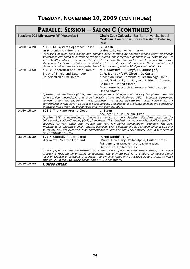
PARALLEL SESSION – SALON C (CONTINUES) Session: 2C3 Microwave/RF Photonics I Chair: Zeev Zalevsky, Bar-Ilan University, Israel
Co-Chair: Lea Singer, Israeli Ministry of Defense, Israel
2C3-1 RF Systems Approach Based on Photonics Architecture
S. Szach Wales Ltd., Ramat-Gan, Israel
14:00-14:20
Processing of wide band signals and antenna beam forming by photonic means offers significant advantages compared to current electronic systems. The integration of optics in RF systems like EW and RADAR enables to decrease the size, to increase the bandwidth, and to reduce the power dissipation far beyond what can be obtained in current electronic systems. Thus, several novel photonic architectures were suggested based on converting analog RF signals into photonics. 2C3-2 Theoretical and Experimental Study of Single and Dual-loop Optoelectronic Oscillators
M. Horowitz1, E. Levy1, O. Okusaga3, C. R. Menyuk2, W. Zhou3, G. Carter2 1Technion-Israel Institute of Technology, Haifa, Israel, 2University of Maryland Baltimore County, Baltimore, United States, 3U.S. Army Research Laboratory (ARL), Adelphi, United States
14:20-14:50
Optoelectronic oscillators (OEOs) are used to generate RF signals with a very low phase noise. We have studied theoretically and experimentally single and dual-loop OEOs. Excellent agreement between theory and experiments was obtained. The results indicate that flicker noise limits the performance of long cavity OEOs at low frequencies. The locking of two OEOs enables the generation of signals with a very low phase noise and with very low spurs. 2C3-3 The Nano-Atomic-Clock L. Stern
Accubeat Ltd, Jerusalem, Israel 14:50-15:10
AccuBeat LTD. is developing an innovative miniature Atomic Rubidium Standard based on the Coherent-Population-Trapping (CPT) phenomena. This standard, named Nano-Atomic-Clock (NAC) is designed for very small size (~10cc) and very low power consumption (360mW). The NAC implements an extremely small “physics package” with a volume of 1cc. Although small in size and power the NAC achieves very high performance in terms of frequency stability: e.g., a few parts of 1e-11/sqrt(tau)(ADEV). 2C3-4 Optically Implemented Microwave Receiver Frontend
P. Herczfeld1, Y. Li2 1Drexel University, Philadelphia, United States 2University of Massachusetts Dartmouth, Dartmouth, United States
15:10-15:30
In this paper we describe research on a microwave optical receiver where analog microwave circuitry is replaced by photonic components. The ultimate goal is to produce an optical-digital receiver capable of providing a spurious free dynamic range of ~140dBHz2/3and a signal to noise ratio of 7dB in the 0 to 20GHz range with a 4 GHz bandwidth.
15:30-15:50 Coffee Break
25
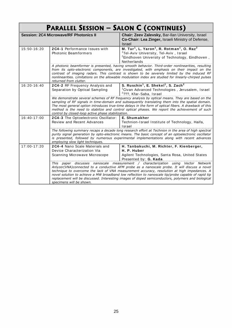
PARALLEL SESSION – SALON C (CONTINUES) Session: 2C4 Microwave/RF Photonics II Chair: Zeev Zalevsky, Bar-Ilan University, Israel
Co-Chair: Lea Zinger, Israeli Ministry of Defense, Israel
2C4-1 Performance Issues with Photonic Beamformers
M. Tur1, L. Yaron1, R. Rotman1, O. Raz2
1Tel-Aviv University, Tel-Aviv , Israel 2Eindhoven University of Technology, Eindhoven , Netherlands
15:50-16:20
A photonic beamformer is presented, having smooth behavior. Third-order nonlinearities, resulting from its opto-electronic components, are investigated, with emphasis on their impact on the contrast of imaging radars. This contrast is shown to be severely limited by the induced RF nonlinearities. Limitations on the allowable modulation index are studied for linearly-chirped pulses returned from clutter. 2C4-2 RF Frequency Analysis and Separation by Optical Sampling
S. Ruschin1, E. Shekel1, S. Zach2
1Civan Advanced Technologies , Jerusalem, Israel 2???, Kfar-Saba, Israel
16:20-16:40
We demonstrate several schemes of RF frequency analysis by optical means. They are based on the sampling of RF signals in time-domain and subsequently translating them into the spatial domain. The most general option introduces true-time delays in the form of optical fibers. A drawback of this method is the need to stabilize and control optical phases. We report the achievement of such control by closed-loop active phase stabilization. 2C4-3 The Optoelectronic Oscillator: Review and Recent Advances
E. Shumakher Technion-Israel Institute of Technology, Haifa, Israel
16:40-17:00
The following summary recaps a decade long research effort at Technion in the area of high spectral purity signal generation by opto-electronic means. The basic concept of an optoelectronic oscillator is presented, followed by numerous experimental implementations along with recent advances employing slow light techniques. 2C4-4 Nano Scale Materials and Device Characterization Via Scanning Microwave Microscope
H. Tanbakuchi, M. Richter, F. Kienberger, H. P. Huber Agilent Technologies, Santa Rosa, United States Presented by: G. Kada
17:00-17:20
This paper discusses nanoscale measurement / characterization using Vector Network Anlyzer(VNA)connected to a conductive AFM probe as a nanoscale probe. It will discuss a novel technique to overcome the lack of VNA measurement accuracy, resolution at high impedances. A novel solution to achieve a MW broadband low reflection to nanoscale tip/probe capable of rapid tip replacement will be discussed. Interesting images of doped semiconductors, polymers and biological specimens will be shown.

26
TUESDAY, NOVEMBER 10, 2009 (CONTINUES)
PARALLEL SESSION– ROYAL H Session: 2D1 Solid State Analog/Mixed-Signal/Digital Circuits and Systems: Part I
Chair: David Gidony Co-Chair: Mark Ruberto Intel Corporation, Israel
2D1-1 A 2.2 GS/s 900 MHz Bandpass Delta-Sigma Modulator for Class-S Power Amplifier
P. Ostrovskyy1, Y. Borokhovych2, G. Fischer3
H. Gustat1, C. Scheytt1 1IHP GmbH, Frankfurt (Oder), Germany 2BTU, Cottbus, Germany, 3Friedrich-Alexander-University Erlangen-Nuremberg, Erlangen, Germany
09:00-09:30
A fourth-order bandpass delta-sigma modulator (BDSM) is designed for operating at decreased sampling frequency to relax the requirements of the power amplification stage in Class-S power amplifier. The modulator is fabricated in 0.25 um SiGe BiCMOS technology and achieves 43.8 dB signal-to-noise ratio (SNR) in 10 MHz bandwidth with sine wave input, while consuming 380 mW from -2.8 V supply. For a WCDMA modulated signal the modulator demonstrates 3 % of EVM. 2D1-2 4-bit, 16 GS/s ADC with New Parallel Reference Network
Y. Borokhovych2, H. Gustat1, J. C. Scheytt1
1IHP, Frankfurt / Oder, Germany, 2Brandenburg University of Technology, Cottbus, Germany
09:30-09:50
This paper presents a high-speed 4 bit full-flash Analog-to-Digital Converter with a new parallel reference network for an UWB radar. The ADC is implemented in 190 GHz SiGe BiCMOS technology, has more than 6 GHz effective resolution input bandwidth and operates up to 16 GSample/s. Power dissipation is 1.15 W including test buffers and 750 mW of the converter itself. 2D1-3 Inter-Symbol Interference (ISI) in On-die Transmission Lines
A. Rysin1, P. Livshits3, S. Sofer1, O. Mantel1, Y. Shapira2, Y. Fefer1 1Freescale Semiconductor Israel Ltd., Herzlia, Israel, 2Tel-Aviv University, Tel-Aviv, Israel 3Bar Ilan University, Ramat Gan, Israel
09:50-10:10
The waveforms of a signal transmitted through single-ended on-die transmission lines, implemented by standard metal layers of a CMOS 45 nm technology node, have been experimentally studied. The influence of the active loss level of the lines, as well as of the impedance mismatch between the transmission line and its driver upon the signal distortion, and particularly upon the inter-symbol interference, is discussed. 2D1-4 Systematic Design of RSSI and Logarithmic Amplifiers Circuits
Y. Melamed, A. Even-Chen, S. J. Spiegel Bar Ilan University, Ramat Gan, Israel
10:10-10:30
This paper presents a systematic design methodology for log amplifier and receiver signal strength indicator circuits. The close expression for the maximum detection error using a piece wise linear approximation of the logarithmic function was derived. A design methodology has been proposed that optimizes the power consumption and bandwidth of a single stage CMOS limiting amplifier according to the input and output common mode voltages to meet the dynamic range and detection error requirements.
10:30-11:15 Coffee Break

27
PARALLEL SESSION – ROYAL H (CONTINUES) Session: 2D2 Solid State Analog/Mixed-Signal/Digital Circuits and Systems: Part II
Chair: Reuven Holtzer, Elipse RFIC Array Devices, Israel Co-Chair: Miki Moyal, Intel Corporation, Israel
2D2-1 A De-Cresting Technique for Polar Transmitters Using Envelope-Tracking (ET) and SiGe Power Amplifiers for Mobile-WiMAX
Y. Li1, D. Meng1, J. Lopez1, D. Y. Lie1, K. C. Chen2, S. Wu2, T. Yang2 1Texas Tech University, Lubbock, United States 2The Industrial Technology Research Institute (ITRI), Hsin-Chu, Taiwan
11:15-11:45
A decresting algorithm for mobile WiMAX has been developed using time domain clipping and filtering processes for a polar transmitter using Envelope-Tracking and a monolithic SiGe power amplifier. RF/Analog/Digital system and circuits co-design simulations have been performed for mobile WiMAX with 64 QAM OFDM modulation. It is found that higher power-to-average ratio decresting can improve the adjacent channel power ratio and overall TX system efficiency, but at the cost of its EVM degradation. 2D2-2 An RSA Processor for Near Real-Time Operation
D. L. Fleischer1, G. Naitzat2, L. Prokupets2 1ADSR, Jerusalem, Israel, 2Technion-Israel Institute of Technology, Haifa, Israel
11:45-12:05
The main challenge in implementing the real time computation of the RSA algorithm is arithmetic computations involving large numbers with thousands of digits. The implementation of our hardware is based on leveraging the use of a CCSA (Carry-Completion-Sensing-Adder). We go over the theoretical and experimental results for custom hardware arithmetic processors and explain how to exploit them to implement an RSA encryption engine for real-time or near real-time operation. 2D2-3 Fast and Noise-Aware Power-Up for On-Die Power Gated Domains
S. Sofer, D. Tzytkin, V. Neiman, E. Melamed-Kohen Freescale Semiconductor Israel Ltd., Herzeliya, Israel
12:05-12:25
The low-noise slow power-up in on-die power-shutoff (PSO) technique limits its usage. Proposed is a method of acceleration of this power-up time, summarized in monitoring of the IR droop of the continuous power supply for holding it at the acceptable level of noise (in contrary to trying to minimize the power-up noise at almost any price). The approach reduces the power-up time with no any functionality impact. 2D2-4 A Non-linear Model for Analysis of Limit Cycle Behavior in CDR with Bang-bang Phase Detector
T. C. Galambos1, V. Lerner2 1PMC-Sierra, Herzliya Pituach, Israel 2Intel, Haifa, Israel
12:25-12:45
We present a method for analysis of the control loop of clock-data recovery circuits (CDR) constructing a non-linear average deviation model that permits fast simulation of the limit cycle behaviors. The average behavior of the non-linear phase detector is modeled using the cumulative density function (CDF) of the total jitter. We present simulation results that show correlation with the long time consuming full circuit simulations.
12:45-14:00 Lunch

28
TUESDAY, NOVEMBER 10, 2009 (CONTINUES)
PARALLEL SESSION – ROYAL H (CONTINUES) Session: 2D3 Power Amplifiers: Design and Devices
Chair: Bumman Kim, Pohang University of Science and Technology, Korea
2D3-1 Design Considerations for GaN Based MMICs
C. F. Campbell, D. C. Dumka, M. Kao TriQuint Semiconductor, Richardson, United States
14:00-14:30
Gallium Nitride (GaN) based transistor technology would appear to be ideally suited to many microwave circuit applications that presently utilize GaAs devices. However, some of the features that make GaN transistors attractive can be shown to create design issues that are typically not encountered with existing low voltage technologies. In this paper specific examples are discussed that highlight some of the potential issues involved with GaN based MMIC design. 2D3-2 Low-Cost High-Efficient 10-Watt X-band High-Power Amplifier
G. van der Bent1, P. de Hek1, A. Bessemoulin2, F. E. van Vliet1 1TNO, The Hague, Netherlands 2Mimix Asia, Hsinchu, Taiwan
14:30-14:50
A high power X-band amplifier with an output power over 10 Watts and a Power Added Efficiency (PAE) in excess of 40 percent has been developed. The design was fabricated in a 0.25 μm pHEMT GaAs process (WIN Semiconductor PP25-01). The small die area in combination with a 6-inch wafer technology provides the possibility for low cost production of a high performance X-band T/R chipset. 2D3-3 Pulsed-Bias Harmonic Load Pull for GaN and Wide Band-Gap Devices
S. Dudkiewicz Maury Microwave Corp, Ontario, United States
14:50-15:10
For the first time, a commercially available pulsed-bias/RF harmonic load pull system is offered for high power and wide band-gap devices. Pulsing DC bias in conjunction with pulsing RF reduces slow long-term memory effects by minimizing self-heating and trapping, giving a more realistic observance of transistor operating conditions. IV, S-Parameter and Load Pull measurements taken under pulsed-bias/RF conditions give more accurate and meaningful results for high-power pulsed applications. 2D3-4 A 40 GHz Power Amplifier Using a Low Cost High Volume 0.15 um Optical Lithography pHEMT Process
K. W. Mays TriQuint Semiconductor, Hillsboro, United States
15:10-15:30
A 40 GHz power amplifier is realized with a new 0.15 um optical lithography pHEMT process developed for low-cost microwave and millimeter wave circuits. Several Ka and V Band market requirements have driven demand for higher bandwidth, low-cost, integrated circuits. A 40 GHz power amplifier is used to demonstrate the process capabilities, starting from the initial design phase and culminating with the fabrication and measurement of the solid state power amplifier.
15:30-15:50 Coffee Break

29
PARALLEL SESSION – ROYAL H (CONTINUES) Session: 2D4 Devices for Communication Applications
Chair: Bumman Kim, Pohang University of Science and Technology, Korea
2D4-1 A +32dBm power amplifier for WiMAX applications in 90nm CMOS
O. Degani, C. Fabian, S. Shahaf, V. Kravstov, D. Chowdhury, C. D. Hull, E. Cohen, R. Shmuel Intel Corporation, Haifa, Israel
15:50-16:10
We demonstrate a single stage 90nm CMOS power amplifier with integrated BALUN for 2.3-2.7GHz WiMAX applications. The PA gain and saturated power are +18dB and +32dBm, respectively, working from a 3.3V supply, with a peak power added efficiency of 48%. Digital pre distortion is used to enhance the PA linearity. The measured EVM for an OFDM signal is improved from -24dB to -30dB at +25dBm output power. Compliance with the FCC 10MHz WiMAX mask is demonstrated at 25dBm with efficiency of ~25%. 2D4-2 Recent Advances in Modeling of Traveling Wave Tubes
D. P. Chernin1, J. J. Petillo1, T. M. Antonsen2, B. Levush3 1SAIC, McLean, United States, 2University of Maryland, College Park, United States, 3Naval Research Laboratory, Washington, United States
16:10-16:30
Traveling wave tubes (TWTs) remain the amplifiers of choice in many applications requiring the production of broadband high frequency microwave and millimeter wave power. All modern TWTs are designed using models that are based on the fundamental physical laws governing the emission, transport, interaction, and collection of electron beams. This paper provides an overview of a state-of-the-art suite of design tools for the end-to-end simulation of coupled-cavity and helix traveling wave tubes. 2D4-3 Evolution of Multi-Octave Helix Travelling Wave Tubes
A. J. Challis, T. K. Ghosh, A. Tokeley, K. Rushbrook, I. Poston, A. Jacob e2v technologies Ltd, Chelmsford, United Kingdom
16:30-16:50
Increasing demands of system integrators and designers, on efficiency and increased capability, have lead to a requirement for higher RF power levels and greater operational bandwidth. This paper describes the design, theoretical modeling and experimental data collated through the development of two multi-octave mini travelling wave tubes (TWTs) during the last 12 months.

30
TUESDAY, NOVEMBER 10, 2009 (CONTINUES)
PARALLEL SESSION – ROYAL I Session: 2E1 Novel RFID Technologies and Systems
Chair: Manos Tentzeris, GEDC, Georgia Tech, United States Co-Chair: Robert Weigel, University of Erlangen-Nuremberg, Germany
2E1-1 RFID-enabled Ultrasensitive Wireless Sensors Utilizing Inkjet-printed Antennas and Carbon Nanotubes for Gas Detection Applications
M. M. Tentzeris1, S. Nikolaou2 1Georgia Tech, Atlanta, United States 2Frederick University, Nicosia, Cyprus
09:00-09:30
This paper presents, for the first time, a conformal CNT-based RFID-enable sensor node for gas sensing applications, fully printed directly on paper substrate. Specifically, in this study one benchmarking RFID tag was designed for the European UHF RFID band centering at 868 MHz. The printed CNT particles were Single-Walled Carbon Nanotubes (SWCNT), which were dispersed in dimethy l formamide (DMF) solution and sonicated to meet the viscosity requirement for the inkjet printer. 2E1-2 UWB Communication System with Pulse Interleaving Multiple Access for Active RFID
D. Raphaeli1, G. Kaplan2 1Tel-Aviv University, Tel-Aviv, Israel 2SandLinks Systems, Petah Tikva , Israel
09:30-09:50
We present a UWB two-way communication system with novel PHY and MAC layers, for low-rate communications with multitude of low-cost devices in ultra low power consumption. The system features a novel multiple access protocol called interleaved impulse radio. 2E1-3 A Novel Software Defined Radio Architecture with Automatic Power Control for RFID Readers
P. Zhao1, Y. Zheng2, T. Hollstein1, K. Fang1, R. Jakoby2, M. Glesner1 1Institute of Microelectronic Systems, Darmstadt University of Technology, Darmstadt, Germany, 2Microwave Research Group, Darmstadt University of Technology, Darmstadt, Germany
09:50-10:10
A novel multi-protocol RFID reader with automatic power control is proposed in this paper based on software defined radio architecture. The transponder power consumption variation over time is considered for different protocols. The modulation effect of power control on forward data transmission is included. The emission power of the reader is tuned in real-time according to the needs of the transponders in compliance with different standards, with which a large amount of power can be saved. 2E1-4 Low Voltage Reference Cells for UHF Transponders With Advanced Features
J. Heidrich1, D. Brenk1, J. Essel1, G. Fischer1, R. Weigel1, G. Hofer2, G. Holweg2
1University of Erlangen-Nuremberg, Erlangen, Germany, 2Infineon Technologies AG, Graz, Austria
10:10-10:30
In this paper a low voltage RC oscillator for RFID applications is presented. Its bias current is provided by a current-mode bandgap whose reference voltage can also be used for enhanced transponder applications. The chip is designed in a 0.12 micrometer CMOS technology with p substrate.
10:30-11:15 Coffee Break

31
PARALLEL SESSION – ROYAL I Session: 2E2 Solid State RFIC Circuits Chair: Mark Ruberto
Co-Chair: David Gidony Intel Corporation, Israel
2E2-1 Designing Analog and RF Circuits in Nanoscale CMOS Technologies: Scale the Supply, Reduce the Area and Use Digital Gates
P. R. Kinget Columbia University, New York, United States
11:15-11:45
We will present our recent research that has centered around three themes aimed at designing analog and RF interface circuits in digital nanoscale CMOS processes. Design techniques for analog and RF circuits operating well below 1V can keep them compatible with future low power digital SOCs. Reclaiming the space under inductors reduces area and cost. Digital gates can facilitate self-calibration for RF front ends to improve performance and simplify design. 2E2-2 An Automatically Matched CMOS Attenuator at C-Band with Improved Control Linearity
U. Mayer, M. Wickert, R. Eickhoff, F. Ellinger Dresden University of Technology, Dresden, Germany
11:45-12:05
In this work, a fully differential CMOS attenuator for C-band comprising matching and control linearization loops is presented. At 5.6 GHz, a total attenuation range of 3.8-29.4 dB was measured. The phase changes only by ±6 ° in an attenuation control range of 15 dB. The control amplifiers draw a total current of 0.54 mA from a single 2.5 V supply. 2E2-3 A Wideband Linear LNA Using Dual-Feedback for TV Tuner
J. Yoon, C. Park, H. Seo, I. Choi, B. Kim Postech, Pohang, Gyungbuk, Republic of Korea
12:05-12:25
This paper represents the wideband LNA using a dual feedback for the tuner application, which can suppress second and third order distortions with a low noise and a high gain. In the dual feedback, the weak negative feedback improves the linearity of the transconductance partially, thereby maintaining the high gain and low noise. The residual distortion and the distortion of the buffer are cancelled by the positive feedback. The proposed LNA improves noise figure and linearity with a high gain. 2E2-4 Constant Loss Miniature 45nm RF-CMOS 24 GHz Phase Shifter
T. Zlotnikov1, O. Degani2, Y. Nemirovsky1
1Technion-Israel Institute of Technology, Haifa, Israel, 2Intel Israel (74) LTD, Haifa, Israel
12:25-12:45
This work presents analysis, optimization, design and characterization of integrated passive phase shifter at 24GHz in a commercially available 45nm RF-CMOS process. This phase shifter excels in extremely low insertion loss variation over phase states and small occupied area making this design attractive for phased array systems applications.
12:45-14:00 Lunch

32
TUESDAY, NOVEMBER 10, 2009 (CONTINUES)
PARALLEL SESSION – ROYAL I Session: 2E3 Solid State Devices Chair: Dan Ritter, Technion-Israel Institute of
Technology, Israel Co-Chair: Emmanuel Cohen, Intel Corporation, Israel
2E3-1 Thermal Management of On-Chip Hot Spots and 3D Chip Stacks
A. Bar-Cohen University of Maryland , College Park , United States
14:00-14:30
Following a brief discussion of the industry roadmap for IC, packaging, and thermal management technology and review of chip package thermal management options, attention will turn to the application of solid-state thermoelectric refrigeration to hot spot remediation. Next, the thermal characteristics of direct immersion cooling in dielectric liquids, a most promising technique for chip stack thermal management, will be explored. 2E3-2 Fast Switching of Drift Step Recovery Diodes Based On All Epi-Si Growth
L. M. Merensky1, I. Shafir1, Y. Sharabani1, D. Eger1, M. Oron1, A. F. Kardo-Sysoev3, D. Shmilovitz2, A. Sher1, A. S. Kesar1
1Soreq NRC, Yavne, Israel, 2Tel-Aviv University, Tel-Aviv, Israel, 3Ioffe Physical Technical Institute, St. Petersburg, Russian Federation
14:30-14:50
DSRDs are fast HV opening switching devices. Traditionally, these deep junction devices are fabricated on silicon wafers by deep diffusion. We present DSRD results based on silicon epitaxial layers with as-grown junctions. Static measurements showed a rectifying behavior with leakage currents proportional to device dimension. Pulsed power measurements showed that the switching rate was dependant on the forward pumping current density. 2E3-3 Electromechanical Behavior of Suspended Taut Single-Walled Carbon Nanotubes
A. Ya'akobovitz, G. Karp, Y. Hanein, S. Krylov Tel-Aviv University, Tel-Aviv, Israel
14:50-15:10
We present an experimental study of the electromechanical behavior of suspended, taut, single walled carbon nanotubes (SWCNTs). A novel fabrication process was developed in order to integrate suspended SWCNTs into silicon structures. The resonant response as well as the electromechanical characterization of metallic-like, small band-gap-like and semiconductor-like SWCNTs under steady electric fields was carried out and high sensitivity of SWCNTs to the gate voltage was observed. 2E3-4 Reliability Status of GaN HEMT Technology for Switch Mode High Power Amplifiers
D. Rozman, Y. Knafo, T. Y. Baksht, O. Aktushev, G. Kolatker, S. Moscovitch, G. Bunin Gal-El (MMIC), Ashdod, Israel
15:10-15:30
We present reliability and failure mechanisms (FM) responsible for the degradation of AlGaN/GaN HEMTs. Particular attention was paid on HEMT working under high drain voltages conditions, 2-3 times higher than operational voltage. This high voltage applied reflects real operational conditions during switch mode operations. DC tests performed in operational conditions placed along load line can simulate RF switch mode operation and allow investigation of relevant degradation mechanisms.
15:30-15:50 Coffee Break

33
PARALLEL SESSION – ROYAL I (CONTINUES) Session: 2E4 Solid State RFIC Circuits and Systems
Chair: Eran Socher, Tel-Aviv University, Israel Co-Chair: Ofir Degani, Intel Corporation, Israel
2E4-1 A High-Performance WiFi/WiMAX Multi-Com RFIC in 90nm CMOS
U. Grosglick, L. Kravitz, D. Ben-Haim, T. Mukatel, S. Zur, E. Goldberger, M. Gordon, G. Horovitz Intel Israel, Petach-Tikva, Israel
15:50-16:20
We present in this article an industry-first multi-com RFIC, combining a dual-band 802.11n radio, supporting up to 3X3 MIMO, and a triple-band 802.16e radio, supporting up to 1X2 MIMO on the same die. This highly-integrated direct-conversion RFIC features an integrated frac-N synthesizer, integrated LNAs and PA drivers, and baseband chains shared by both TX and RX chains. Calibration circuits and control flexibility ensure consistent performance under production and environmental variations. 2E4-2 Fully Integrated Active CMOS Vector Modulator for 802.11a Compliant Diversity Transceivers
N. Joram, U. Mayer, R. Eickhoff, F. Ellinger Dresden University of Technology, Dresden, Germany
16:20-16:40
A CMOS vector modulator designed for smart antenna arrays at 5.5 GHz is presented. A quadrature all pass filter and sign select switches yield two orthogonal signal paths. Two variable gain amplifiers with strongly reduced phase shift of only ±6° are used to weight these paths. Phase control range is 360° and gain range is -20 dB to 2.8 dB. The IIP3 is -7 dBm at maximum gain. The current drawn from a 1.5 V supply amounts 12 mA. Using a 180 nm technology, the chip core area is 1.2x0.8 mm². 2E4-3 A Design Approach for the Minimization of Self-Interference Effects in Highly Integrated Transceiver SoCs
O. E. Eliezer1,2, B. R. Staszewski1,3, P. T. Balsara2 1Texas Instruments , Dallas, United States, 2University of Texas at Dallas, Richardson, United States, 3TU Delft, Richardson, United States
16:40-17:00
A design methodology is introduced to minimize the productization duration and costs for highly integrated transceiver SoCs comprising extensive digital circuitry, mixed signal and sensitive RF blocks, resulting in a high potential for self-interference within the SoC. The methodology and derived techniques rely on resources available in the SoC at negligible cost for coordinating the operation of internal functions and for implementing means to mitigate the impact of self-interference. 2E4-4 A 360 Degree Phase Shifter for 60 GHz Application in SiGe BiCMOS Technology
Y. Sun, C. Scheytt IHP, Frankfurt (Oder), Germany
17:00-17:20
This paper presents a voltage controlled phase shifter in a 0.25 um SiGe BiCMOS technology for 60 GHz applications. Vector combination technique is adopted in phase shifter core. Continuous 360 degree phase tuning from 40 GHz to 70 GHz has been measured. The insertion gain of the complete test circuits is 4.6 dB and that of the phase shifter core is 7.6 dB. The phase shifter is best suited for 60 GHz phased array systems.
PARALLEL SESSION – ROYAL J Session: 2F1 GHN – The IEEE Global History Network
2F1-1 GHN – The IEEE Global History Network
J. Baal-Schem Tel-Aviv University, Tel-Aviv, Israel
09:45 – 10:30
In September 2008, the IEEE History Committee launched the Global History Network (GHN) at the IEEE Section Congress in Montreal, Canada. The IEEE Global History Network (GHN) intends to be the world’s premier site for the documentation, analysis and explanation of the history of electrical, electronic, and computer technologies, the scientists, engineers and business people who made these technologies happen, and the history of the organizations to which these men and women belonged.
10:30 – 11:15 Coffee Break

34
TUESDAY, NOVEMBER 10, 2009 (CONTINUES)
PARALLEL SESSION – ROYAL J (CONTINUES) Session: 2F2 RF MEMS Devices and Sensors Chair: Yael Nemirovsky,
Technion-Israel Institute of Technology, Israel 2F2-1 Microcantilevers as Artificial Nose Platform
A. Shemesh, Y. Eichen, S. Stolyarova, Y. Nemirovsky Technion-Israel Institute of Technology, Haifa, Israel
11:15-11:35
In recent years, explosive based terrorism has grown enormously; moreover, chemical warfare is forecasted as next terror inflicting agent. Detecting such materials is a challenging task. Aiming towards artificial nose, we take advantage highly sensitive porous-silicon microcantilevers devices in combination of non specific layers and monitor their interaction with target analytes. Our screening method is through passive detection and an active one and has proved for sensing different isotopes. 2F2-2 Multi-Cantilever HEMT-based Resonant Sensor
I. Khmyrova1, E. Shestakova2 1University of Aizu, Aizu-Wakamatsu, Japan 2Moscow State University of Environmental Engineering, Moscow, Russian Federation
11:35-11:55
In this paper resonant sensor based on micro-machined high-electron mobility transistor (HEMT) in which multiple suspended resonant cantilevers serve as floating gates is proposed and its analytical and lumped equivalent circuit models are developed. The proposed HEMT-based multi-cantilever resonant sensor enables electrostatic actuation and electrical read-out. 2F2-3 High Tuning Range MEMS Capacitor for Microwave Applications
E. David, T. Zlotnikov, L. Gal, O. Lavie, Y. Nemirovsky Technion – Israel Institute of Technology, Haifa, Israel
11:55-12:15
This paper presents a new MEMS comb-structured variable capacitor that features a wide capacitance tuning range, yet avoids unwanted coupling through the springs. This novel varactor consists of three comb structures - two of which are anchored to the substrate, while the third, which capacitively couples the two anchored ones, is movable, suspended on mechanical springs. This new design decouples the mechanical mechanism from the RF capacitor and allows an independent optimal design of the two. 2F2-4 High Performance MEMS 0.18um RF-CMOS Transformers
S. Katz1, I. Brouk1, S. Stolyarova1, S. Shapira2, Y. Nemirovsky1 1Technion – Israel Institute of Technology, Haifa, Israel, 2TOWER Semiconductor Ltd., Migdal Haemek, Israel
12:15-12:35
This work presents a MEMS RF-CMOS transformer fabricated in a commercially available 0.18um CMOS process provided by Tower Semiconductor Ltd.. Maskless micromachining post-processing is used to remove oxide and substrate material from around the transformer. The resulting increases in quality factor and self-resonant frequency enable the transformer’s use in more designs and at higher frequencies than is possible without micromachining.
12:35-14:00 Lunch

35
PARALLEL SESSION – ROYAL J (CONTINUES) Session: 2F4 Cognitive Radio, SDR and Smart Antennas
Chair: Jeffrey H. Reed, Virginia Tech, United States
2F4-1 System Power Consumption Minimization for Multichannel Communications Using Cognitive Radio
A. He1, S. Srikanteswara2, K. K. Bae3, T. R. Newman1, J. H. Reed1, W. H. Tranter1, M. Sajadieh4, M. Verhelst2 1Virginia Polytechnic Institute and State University, Blacksburg, United States 2Intel Corp., Hillsboro, United States 3Liberty University, Lynchburg, United States 4Intel Corp., Santa Clara, United States
14:00 – 14:30
This paper presents a methodology and framework to minimize system power consumption for multichannel communications using cognitive radio (CR) based on the application quality of service requirement, the channel condition, and the radio capabilities and characteristics. Simulation results show that the knowledge of the radio capabilities and characteristics can help to reduce system power consumption significantly (e.g., up to 55% for a multichannel system with Class A power amplifiers). 2F4-2 Directional Antennas and Radio Networks
N. Love1, L. H. Jones2, S. Stegmann3 1Interactive Technology Solutions, Silver Spring, United States, 2University of Maryland, College Park, United States, 3Stegmann Engineering, Elkridge, United States
14:30-14:50
Simply attaching one or more directional antennas to a conventional radio system will increase cost without producing a radio capable of forming a functioning network. Many of the difficulties in integrating smart adaptive antennas into an SDR are artifacts of the OSI Reference Model. This paper outlines the fundamental challenges involved in integrating directional antennas into radio networks and explores some of the currently available technical approaches. 2F4-3 Dynamically-Configurable Multimode Transmitter Systems for Wireless Handsets, Cognitive Radio and SDR Applications
R. Harlan, G. Rawlins, D. Sorrells ParkerVision Inc., Jacksonville, United States
14:50-15:10
A unified transmit chain for handsets, SDR, and cognitive radio addresses the need for an efficient low-cost multimode solution. The 65nM CMOS control block contains a small state machine that interprets I/Q data inputs and selects settings from memory, which are based on characterization of the modulating device for the operating regime. Nonlinear functions map the desired output into control signals that manipulate a 130nM-SiGe vector-power-modulator to construct a full-power RF waveform.

36
TUESDAY, NOVEMBER 10, 2009 (CONTINUES)
PARALLEL SESSION – FOYER Session: 2G3 Poster Session II
2G3-1 Distortion Mechanisms in Supply Modulation of Polar Transmitters
M. Alon1, S. Singer1, S. J. Spiegel2 1Tel-Aviv University, Tel-Aviv, Israel 2Rio Systems Ltd, Tel-Aviv, Israel
The distortion mechanisms in supply modulation introduced by the PWM generator, the frequency response of DC regulator and the limited bandwidth of the high frequency recovery unit are analyzed for EDGE polar transmitters. It is demonstrated that there is an optimum regulator bandwidth that minimizes the total residual energy originated from the PWM generator and the low pass filter characteristics of the buck converter 2G3-2 Cutoff Wavelengths of Metallic Waveguides with Elliptical Cross Section
G. D. Tsogkas1, J. A. Roumeliotis1, S. P. Savaidis2
1National Technical University of Athens, Athens, Greece, 2Technological Educational Institute (TEI) of Piraeus, Athens, Greece
The cutoff wavelengths λcmn of metallic waveguides with elliptical cross section are determined analytically. Two alternative methods, namely, a field and a shape perturbation method are used in the proposed analysis. Exact, closed form expressions, free of Mathieu as well as of Bessel functions, are obtained for the cutoff wavelengths, when the solution is specialized to small values of the eccentricity of the elliptical cross section. Numerical results for all types of modes are also included. 2G3-3 Fibers vs. Coax for RF Delay Line Applications
E. Granot1,2, R. Weber1, S. Tzadok1, G. Gertel1, N. Narkiss1
1Finisar-Israel, Nez-Ziona, Israel 2Ariel University Center of Samaria, Ariel, Israel
A comparison between the RF-over-fiber and the RF-over-coax technologies is presented. It is shown that while in relatively short delay lines the coax technology will do, for delay lines longer than a certain distance the fiber technology has a clear advantages: Beyond several microseconds it is better in terms of volume, Noise Figure and cost. 2G3-4 Overview of Wireless Miniature RF-Photonic Sensors Networks WRPN
A. Amarant RST, Ra'anana, Israel
A variety of both Defense and Commercial applications involve the use of a large number of miniature sensors of various types (acoustic, photonic, magnetic, RF, mechanical, etc) that are spread over the areas of interest and need to report the information gathered to a central point. As cable interconnection is not feasible and/or economical a wireless network is utilized. This paper describes a WRNP system that includes miniature wireless transceivers integrated with various sensors. 2G3-5 The Development of Wireless Indoor Security System with Protection Against "Qualified Bypass"
T. Galeev KSTU, Kazan, Russian Federation
In given report is presented experience of the development of the system, which has a high stability radio communication and protection against "qualified bypass. This is a first Russian indoor wireless security system. In addition, the system was certificated in Germany under trademark “Controlex”. 2G3-6 Current Sensing with a Precision of a Few Parts per Million within a Faction of a Second
J. Szwarc Vishay Intertechnology / Vishay Israel, Holon, Israel
The key to a precise and fast measurement of changes in electrical current is the use of current sensing resistors which are not influenced by the magnitude of the current flowing through it, or by changing ambient temperature, or by other environmental conditions. This is achieved by applying a “Z foil”, having a Temperature Coefficient of Resistance of 0.2 ppm/°C to two sides of resistor chip’s substrate: Under rated power the resistance drifted 1ppm after 1 second and 5ppm after 9s. 2G3-7 Use of Time Domain Methods for CISPR16 Compliant EMI Measurements
H. G. Westenberger Rohde & Schwarz International Operations GmbH, Munich, Germany
09:30-15:30
A common problem with EMI measurements using conventional time-saving procedures is that in most cases the total measurement time is still very long. A significant reduction of the measurement time is possible when using time-domain methods that determine the interfering spectrum by means of the digital fast Fourier transform. The paper describes the principles, major problems and how they are solved without missing any inferring signal or without losses in accuracy.

37
PARALLEL SESSION – FOYER (CONTINUES) Session: 2G3 Poster Session II
2G3-8 A Novel Photonic Rotman-Lens Design for Radar Phased Array Antennas
Z. Zalevsky1, S. Zach2, M. Tur3 1Bar-Ilan University, Ramat-Gan, Israel 2Consultant, Kfar Saba, Israel 3Tel-Aviv University, Tel-Aviv, Israel
A novel photonic Rotman-lens design for Radar phased array antennas is proposed. The proposed photonic configuration for the Rotman lens is capable of realizing a linear phase profile with a varied slope, that is obtained at the output of the lens for any possible position at the input to the lens. This is in contrast to what is currently available with the conventional RF Rotman lens, where output phase front linearity is obtained for a small and discrete number of input positions. 2G3-9 A Packaged X-Band Low Noise Amplifier
N. Snir, N. Bar-Helmer, R. Pasternak, D. Regev Elipse RFIC Array Devices, Kfar Neter, Israel
The design of a high dynamic range LNA at X band frequency involves challenges and different product and circuit aspects. Package and parasitic must be included as the impact on performance is significant. 200GHz SiGe Technology was chosen to support frequency of operation, noise levels and linearity requirements. RF grounding metal mesh methodology was employed to support grounding needs. 2G3-10 Investigation of Synchronization System in a Framework of Measurements of Microwave Phase Progression on a Opened Links
I. B. Shirokov, Y. B. Gimpilevich, I. V. Serdyuk Sevastopol National Technical University, Sevastopol, Ukraine
Presented paper is devoted to experimental investigation of transferring of initial phase of low frequency oscillations with modulation of carrier oscillations in separate high frequency link from one part of testing link to another. The block diagram of the device, the results of calculations and experimental investigations for reference and lock-in oscillators are given in the paper. Also the spectrogram of noises for different pseudorandom sequences features is given. 2G3-11 A 60GHz Radio-over-Fiber Architecture for the Transmission of UWB-OFDM Signals
M. Benzazaa1, F. Deshours1, C. Algani2, G. Alquié1, F. Mandereau2, A. Billabert2 1UPMC, Paris, France, 2Cnam, Paris, France
This paper presents an 60 GHz architecture for UWB RoF systems to increase transmission distances and high data bit rates. This architecture allows to send through an optical fiber both a subcarrier microwave signal and UWB baseband data by using a wavelength multiplexer. At the base station, the carrier frequency is photodetected, modulated by data and then up-converted to millimeter-wave band. Simulation results using VPI systems software are reported and discussed for OFDM signals. 2G3-12 Photonic Configuration for Spectrally and Directionally Tunable Tera-Hertz Radiation Source
A. Rudnitsky, S. Zach, Z. Zalevsky
1Bar-Ilan University, Ramat-Gan, Israel
We propose a photonic configuration for generation of directional THz radiation source using non collinear two waves mixing process. The proposed device also allows controlling the frequency of the generated radiation source. The main application of the discussed configuration is for microwave photonic systems. 2G3-13 Cognitive Sensor Array for Geophysics
G. Dekoulis Lancaster University, Lancaster, United Kingdom
This paper describes a miniature sensor array for geophysics. Performance is predicted by a quantitative mathematical model based on linear relationships. The dependence of the output voltage on the specifications is obtained by implementing a Fourier analysis of the captured data. The array is using a new cobalt-based material not previously used in geophysics. Array electromagnetic simulations verify that the set specifications. 2G3-14 Active RFID TAGs System Analysis of Energy Consumption As Excitable Linear Bifurcation System
O. Aluf Future Electronics , Herzeliya, Israel
Active RFID TAGs system energy analysis as excitable linear bifurcation system. Active RFID TAGs have a built in power supply. The Active RFID TAG equivalent circuit can be represent as a differential equation which depending on variable parameters. The investigation of Active RFID's differential equation based on bifurcation theory, the study of possible changes in the structure of the orbits of a differential equation depending on variable parameters. using excitable bifurcation diagram.
09:30-15:30
2G3-15 A Cavity Backed Tunable Slot Antenna (CBSA) for Close Proximity Biomedical Sensing Applications
Q. Bonds1, T. Weller1, B. Roeder2, P. Herzig2 1University of South Florida, Tampa, United States, 2Raytheon Co, Largo, United States
Presented is a Cavity Backed Slot Antenna (CBSA) designed for integration into a biomedical radiometric sensor intended for close proximity health monitoring applications. An internal probe feed adds a novel approach to biomedical antenna design by isolating antenna feed currents from the body and providing frequency tuning of ~50MHz/mm as a function of probe length. Measurements and simulations were performed with the CBSA in close proximity to a skin tissue phantom.

38
WEDNESDAY, NOVEMBER 11, 2009
PARALLEL SESSIONS
PARALLEL SESSION – ROYAL H Session: 3A1 Tutorial Session I Chair: Arie Reichman, Ruppin Acdemic Center,
Israel 3A1-1 RFID Tutorial (RFID Overview of Technologies, Applications and Roadmap)
I. Kalman Eltav Wireless Monitoring, Ra’anana, Israel
09:15-10:00
This tutorial presents an overview of RFID technologies and implementations consisting of: 1) RFID Technology introduction (passive, active, semi active, battery assisted, frequency bands, standards and regulations, capabilities and limitations) 2) RFID Technology History 3) RFID Technology Road Map 4) Example Applications 5) Market Overview 3A1-2 Tutorial – Modern Transceiver Design for RFIC Based Applications
A. Zafrany Amimon Ltd, Herzelia, Israel
10:00-10:45
This paper introduces practice considerations for design and analyze direct conversion transceiver for RFIC applications. Direct conversion transceiver is the most popular architecture today for RFIC implementation where low cost, low current solutions are required.
10:45-11:15 Coffee Break
Session: 3A2 Tutorial Session II Chair: Arie Reichman, Ruppin Academic Center, Israel
3A2-1 Cooperative Communication O. Amrani Tel-Aviv University, Tel-Aviv, Israel
11:15-12:00
A tutorial on cooperative communication techniques.
3A2-2 Key Challenges in Femtocells Deployment
Y. Volloch Percello, Raanana, Israel
12:00-12:45
Femtocells are low-cost, low-power wireless access points that operate in licensed spectrum to connect standard mobile devices to a mobile operator’s network using broadband connections. The challenges associated with a mass market femtocell are significant. Percello provides innovative and customized solutions that address the key business and technological challenges in the emerging Femtocell market.
12:45-14:00 Lunch Session: 3A3 Tutorial Session III Chair: Arie Reichman, Ruppin Academic Center,
Israel 3A3-1 International Mobile Telecommunications – Advanced. Tutorial Highlights
A. Freedman Nice Systems Ltd., Petach-Tikva, Israel
14:00-14:45
IMT-Advanced is an ITU concept for mobile communication systems with capabilities which go further than that of IMT-2000 systems. Currently this is a name of a process rather than detailed technical specifications, to lead and coordinate the international standards towards the 4th generation mobile communication systems. The tutorial describes the vision and requirements for IMT-Advanced and explains the process and its schedule. Finally technical specifications of main candidates are described. 3A3-2 Long-Term Evolution Network Architecture
R. Nossenson RNWC, Kfar-Sava, Israel
14:45-15:30
This paper provides a technological overview of the System Architecture Evolution (SAE) of LTE networks. The target of this overview is to provide a basic knowledge on 4G cellular network structure, entities responsibilities and protocol-stack. The overview is mainly based on the relevant 3GPP standards and on Chapter 3 of the book "LTE for UMTS: OFDMA and SC-FDMA Based Radio Access" edited by Harri Holma and Antti Toskala.
15:30-15:50 Coffee Break Session: 3A4 Tutorial Session IV Chair: Arie Reichman, Ruppin Academic Center,
Israel 3A4-1 A Quick Introduction to MIMO Technology
D. Ezri Greenair Wireless, Ramat Gan, Israel
15:50-17:20
MIMO technology provides a powerful tool for enhancing the wireless link and has already been incorporated into the WiMAX and LTE standards. In this talk we abandon the classical information theoretic approach to MIMO and discuss the technology from the view point of a communications practitioner, focusing on the performance gain and implementation complexity of various schemes. Finally we discuss the fusion of MIMO and OFDM and compare the performance of MIMO modes in

39
practical systems.
PARALLEL SESSION – ROYAL I Session: 3B1 Short Course on Nanoplasmonics Moderator: M. I. Stockman
Georgia State University, Atlanta, United States 09:15-10:45 3B1-1 This short course is designed to be an introduction and review of the modern
state of nanooptics and nanoplasmonics. Additionally it will provide a discussion and significant focus on advanced applications. The physics of surface plasmons, including the concentration of energy on the nanoscale, control of nanooptical phenomena, and ultrafast and nonlinear nanoplasmonics will be discussed.
10:45-11:15 Coffee Break 11:15-12:45 3B2-1 Nanoplasmonics: Short Course on the Optical Properties of Metal Nanostructures
(Continues) 12:45-14:00 Lunch 14:00-15:30 3B3-1 Nanoplasmonics: Short Course on the Optical Properties of Metal Nanostructures
(Continues) 15:30-15:50 Coffee Break 15:50-17:20 3B4-1 Nanoplasmonics: Short Course on the Optical Properties of Metal Nanostructures
(Continues)