Packaging and Interconnect Technologies for Cryogenic ...
24
IEEE Santa Clara Valley Chapter, Electronics Packaging Society April 22, 2021 www.ieee.org/scveps 1 Approach Packaging and Interconnect Technologies for Cryogenic & Quantum Systems Dr. Michael C. Hamilton Electrical and Computer Engineering, Auburn University Alabama Micro/Nano Science and Technology Center (AMNSTC) IEEE Silicon Valley / SF Bay Area EPS Chapter Webinar, April 22 nd , 2021 Approach 2 Outline • Intro Comments & Overview • P&I for Cryogenic Electronics • Superconducting resonators • Interconnects (Superconducting Flex Cables) • Connectors (Cable-to-Cable) • Moving towards Quantum • Very brief intro to “quantum” • Challenges • Approaches • Concluding Comments
Transcript of Packaging and Interconnect Technologies for Cryogenic ...

IEEE Santa Clara Valley Chapter, Electronics Packaging Society
April 22, 2021
www.ieee.org/scveps 1
Approach
1
Packaging and Interconnect Technologies for Cryogenic &
Quantum Systems
Dr. Michael C. Hamilton
Electrical and Computer Engineering, Auburn University
Alabama Micro/Nano Science and Technology Center (AMNSTC)
IEEE Silicon Valley / SF Bay Area EPS Chapter
Webinar, April 22nd, 2021
Approach
2
Outline
• Intro Comments & Overview
• P&I for Cryogenic Electronics• Superconducting resonators• Interconnects (Superconducting Flex Cables)• Connectors (Cable-to-Cable)
• Moving towards Quantum• Very brief intro to “quantum”• Challenges• Approaches
• Concluding Comments
IEEE Santa Clara Valley Chapter, Electronics Packaging Society
April 22, 2021
www.ieee.org/scveps 2
Approach
3
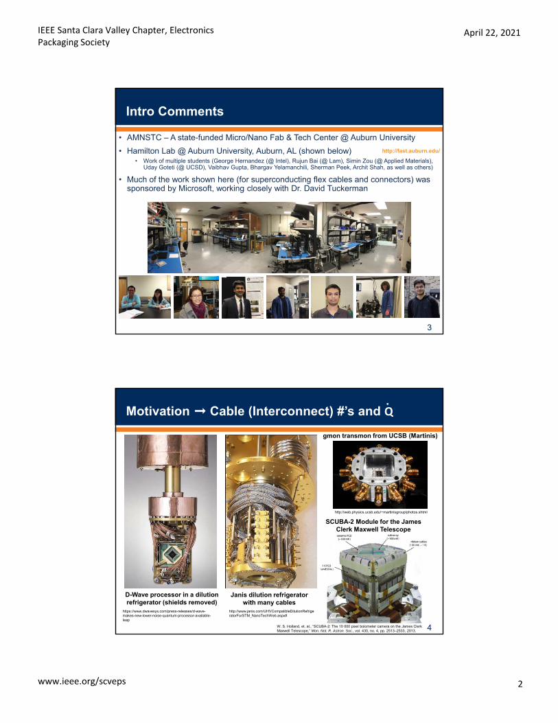
Intro Comments
• AMNSTC – A state-funded Micro/Nano Fab & Tech Center @ Auburn University
• Hamilton Lab @ Auburn University, Auburn, AL (shown below)• Work of multiple students (George Hernandez (@ Intel), Rujun Bai (@ Lam), Simin Zou (@ Applied Materials),
Uday Goteti (@ UCSD), Vaibhav Gupta, Bhargav Yelamanchili, Sherman Peek, Archit Shah, as well as others)
• Much of the work shown here (for superconducting flex cables and connectors) was sponsored by Microsoft, working closely with Dr. David Tuckerman
http://fast.auburn.edu/
Approach
4
D-Wave processor in a dilution refrigerator (shields removed)
https://www.dwavesys.com/press-releases/d-wave-makes-new-lower-noise-quantum-processor-available-leap
gmon transmon from UCSB (Martinis)
http://web.physics.ucsb.edu/~martinisgroup/photos.shtml
SCUBA-2 Module for the James Clerk Maxwell Telescope
W. S. Holland, et. al., “SCUBA-2: The 10 000 pixel bolometer camera on the James Clerk Maxwell Telescope,” Mon. Not. R. Astron. Soc., vol. 430, no. 4, pp. 2513–2533, 2013.
http://www.janis.com/UHVCompatibleDilutionRefrigeratorForSTM_NanoTechWeb.aspx#
Janis dilution refrigerator with many cables
Motivation ➞ Cable (Interconnect) #’s and Q

IEEE Santa Clara Valley Chapter, Electronics Packaging Society
April 22, 2021
www.ieee.org/scveps 3
Approach
5
IBM / Google / Intel (among others!)
Google and https://phys.org/news/2020-08-google-largest-chemical-simulation-quantum.htmlIBM and https://spectrum.ieee.org/tech-talk/computing/hardware/ibms-quantum-leap-simulates-56qubit-machine
Intel
Intel Tangle Lake& Horse Ridge II
GoogleBristlecone& Sycamore
IBM Hummingbird
Approach
6
Intro / Background
• In much of this work, where possible, we’ve used superconductors (SC):
• Ultra-low (but not zero) loss below Tc @ microwave frequencies• (Surrounding) dielectric loss (tan) important, comparable to SC loss• Impedance matching similar to non-SC, but sometimes need to take
kinetic inductance (Lk) into account• EM simulators (i.e., ADS, HFSS, Sonnet, etc.) with proper SC model
• Example trace density of SC cables*:• Single layer of single-ended stripline: 5 m thick PI, ~ 5 m wide traces,
5 m vias, 20 m space between traces and vias…pitch ~ 50 m => 200 single-ended / cm (of width) [< 10 nW for 4K-10mK]
• Need sufficient grounding between signals to reduce crosstalk and allow impedance matching up to very high frequencies (> 100 GHz)
• Challenge to fan-out/break-out to (available) connectors• Working to scale to this level, expand to multi-layer, 2D break-out, etc.
* Not what will be shown today, just for motivating the topic
IEEE Santa Clara Valley Chapter, Electronics Packaging Society
April 22, 2021
www.ieee.org/scveps 4
Approach
7
• Cables with 19 m thick PI-2611
• 10 DC traces per cable
• Nb with Ti adhesion
• Ti/Ni/Cu/Au UBM
Previous Nb & NbTi Superconducting Flex Cables
FLEX
PCB
Cross-section
Superconducting transition
Van Weers et al., Cryogenics 55, 1-4 (2013).
• NbTi foil laminated to Kapton
• Up to 40 cm long and up to 10 traces per cable
• Loss of 2.5 dB and cross-talk of -25 dB obtained at 8 GHz
Walter et al., IEEE Trans. Appl. Supercond., 28(1), 1-5 (2018).
Approach
8
• Nb47Ti coaxial ribbon cable terminated with G3PO connectors
• 30 cm long, 1 dB loss at 8 GHz and -60 dB nearest neighbor cross-talk
• Heat load of 20 nW from 1 K to 90 mK –Roughly half the load from the smallest commercially available SC coax
Previous Nb & NbTi Superconducting Flex Cables
Close-up of cable end
Fully assembled cable between
temperature stages
Schematic showing cable attachment to G3PO connectors via capillary tube
Smith et al., IEEE Transactions on Applied Superconductivity, 31(1), 1-5 (2020).
S21 measurement of the traces at 4 K
S41 at 4 K (avg. crosstalk indicated in red dashed line)

IEEE Santa Clara Valley Chapter, Electronics Packaging Society
April 22, 2021
www.ieee.org/scveps 5
Approach
9
• 33 traces, 200 μm wide MgB2 on flexible YSZ
• Delamination of MgB2 when exposed to water at RT
• Improved by using ALD deposited Al2O3
High(er) Tc Superconducting Flexible Cables
MgB2 FFC before and after mating to a
Hirose FFC/FPC connector assembly
R vs T plot showing a Tc of ~ 37 K
Yung et al., IEEE Trans. Appl. Supercond., 21(3), 107-110 (2010).
Signal lines
Assembled tape
• YBCO films exfoliated and transferred to Kapton
• < 1dB/m attenuation @ 6GHz & 77K
Solovyov et al., No. BNL-220992-2021-JAAM (2021).
Approach
10
Outline
• Intro Comments & Overview
• P&I for Cryogenic Electronics• Superconducting resonators• Interconnects (Superconducting Flex Cables)• Connectors (Cable-to-Cable)
• Moving towards Quantum• Very brief intro to “quantum”• Challenges• Approaches
• Concluding Comments
IEEE Santa Clara Valley Chapter, Electronics Packaging Society
April 22, 2021
www.ieee.org/scveps 6
Approach
11
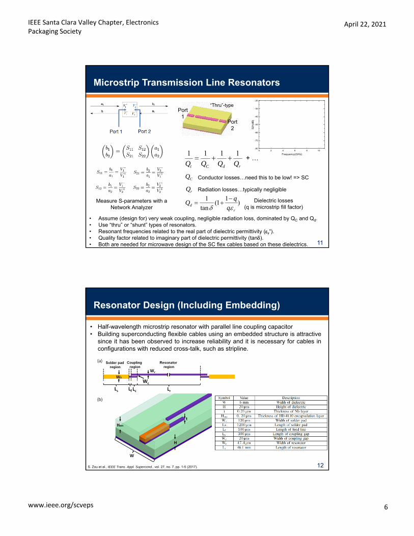
Microstrip Transmission Line Resonators
0 2 4 6 8 10-80
-70
-60
-50
-40
-30
-20
S21
(dB
)
Frequency(GHz)
• Assume (design for) very weak coupling, negligible radiation loss, dominated by QC and Qd.• Use “thru” or “shunt” types of resonators.• Resonant frequencies related to the real part of dielectric permittivity (r’).• Quality factor related to imaginary part of dielectric permittivity (tan).• Both are needed for microwave design of the SC flex cables based on these dielectrics.
rdCt QQQQ
1111
CQ Conductor losses…need this to be low! => SC
)1
1(tan
1
rd q
rQ Radiation losses…typically negligible
Dielectric losses(q is microstrip fill factor)
+ …
Port1
Port2
Measure S-parameters with a Network Analyzer
“Thru”-type
Approach
12
Resonator Design (Including Embedding)
• Half-wavelength microstrip resonator with parallel line coupling capacitor• Building superconducting flexible cables using an embedded structure is attractive
since it has been observed to increase reliability and it is necessary for cables inconfigurations with reduced cross-talk, such as stripline.
S. Zou et al., IEEE Trans. Appl. Supercond., vol. 27, no. 7, pp. 1-5 (2017).

IEEE Santa Clara Valley Chapter, Electronics Packaging Society
April 22, 2021
www.ieee.org/scveps 7
Approach
13
Flexible Microstrip Fabrication Process Flow
After step 7
After assembly
• PI layers ~ 20 μm, Nb layers ~ 250 nm• Previously used Cr/Al (barrier/sacrificial) layers on top of Si handle wafer, for release of nearly complete sample (then back-side Nb deposition)• Moved to fused silica wafers and (excimer) laser release (without Cr/Al layers)
Approach
14
LHe Dewar (4.2 K)
T = 4.2 K Sample rod
Teflon flange
SMA connectors
Dewar rod with SMA connectors and sample holder
Pulse-tube CryostatT = ~ 1.2 K to 300 K
Calibration @ Cryo
Cryogenic Microwave Measurement Setups
IEEE Santa Clara Valley Chapter, Electronics Packaging Society
April 22, 2021
www.ieee.org/scveps 8
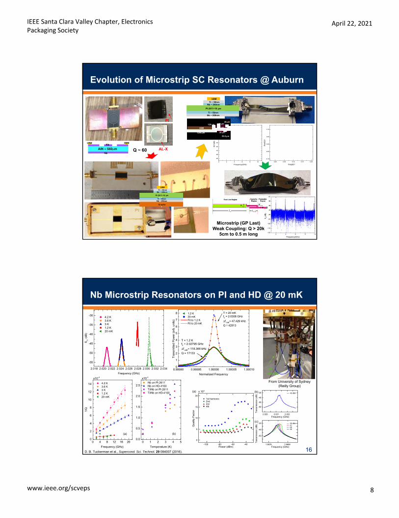
Approach
15
Q ~ 60
PI
AL-X
0 2 4 6 8 10
-90
-80
-70
-60
-50
-40
-30
-20
-10
S2
1(d
B)
Frequency(GHz)
0.00 0.05 0.10 0.15 0.20
-0.10
-0.05
0.00
0.05
0.10
Rea
lS2
1
ImagS21
PI-2611~10 µm
Nb ~ 250nm
UBM
Ti ~ 50nm
Ti ~ 50nmNb ~ 250nm
Si wafer
PI-2611~10 µm
Nb ~ 250nm
UBM
Ti ~ 50nm
Ti ~ 50nmNb ~ 250nm
120 μm
UBM
1200 μm
40 μm
20 μm
40 μm
350 μm
50.6 μm
Microstrip (GP Last)Weak Coupling: Q > 20k
5cm to 0.5 m long
Evolution of Microstrip SC Resonators @ Auburn
Approach
16
Nb Microstrip Resonators on PI and HD @ 20 mK
From University of Sydney (Reilly Group)
Our sample
Frequency (GHz)
Tra
nsm
issi
on (
dB)
Power (dBm)
Qua
lity
Fac
tor
Frequency (GHz)
Tra
nsm
issi
on (
dB)
-30
-40
-50
-30
-40
-50
2.020 2.0222.021
-60
1.9676 1.9684
5
20
15
10
-40-60-80-100
1st harmonic
4th3rd2nd
(a)
(c)
(b)
-36 dBm
-56-46-41
x 103
0
-40 dBm
D. B. Tuckerman et al., Supercond. Sci. Technol. 29 084007 (2016).

IEEE Santa Clara Valley Chapter, Electronics Packaging Society
April 22, 2021
www.ieee.org/scveps 9
Approach
17
SC Stripline Resonators
• Stripline transmission line resonators from different batches and different wafers.• Resonators baked in vacuum oven at 90 oC for 2 hrs and then measured in PT cryostat.• Q for different stripline resonators are relatively comparable and show that the additional
fabrication processes can be tolerated (Nb not significantly deteriorated).• Showed repeatability, process stability and promise for extension to additional signal layers.
V. Gupta et al., IEEE Trans. Appl. Supercond., vol. 29, no. 5, pp. 1-5 (2019).
HD4110 ~ 20um @ 225°C
HD4100 ~ 10um @ 375°CAl/Nb/Al (Bottom Ground)
Al/Nb/Al (Signal)Ti/CuTi/Cu
Cu
Cu
Cu
HD4110 ~ 20um @ 225°C
Ti/Cu Ti/Cu
Cu
HD4100 ~ 4um @ 225°CAl/Nb/Al (Top Ground)
Ti/Cu/Au Ti/Cu/Au
Approach
18
Outline
• Intro Comments & Overview
• P&I for Cryogenic Electronics• Superconducting resonators• Interconnects (Superconducting Flex Cables)• Connectors (Cable-to-Cable)
• Moving towards Quantum• Very brief intro to “quantum”• Challenges• Approaches
• Concluding Comments

IEEE Santa Clara Valley Chapter, Electronics Packaging Society
April 22, 2021
www.ieee.org/scveps 10
Approach
19
Microwave Calibration at ~ 4 K
Open Short RF Resistor
Calibration standards based on Southwest Microwave edge
launch connectors
Close-up of a 50 Load
• Super low loss expected for SC cables…need excellent calibration.• SOLR calibration => 4 mechanical standards for Short / Open / Load /
Reciprocal-Thru.• Thru can be any reciprocal thru, including the sample (must be reciprocal).• Four cool-downs to calibrate two ports.• Move to RF switches => 1 cool-down.
Representative thru: sample
G. A. Hernandez et al., IEEE Trans. Appl. Supercond., vol. 27, no. 4, pp. 1-4 (2017).
Approach
20
Stripline w/spin-on PI(1 meter)
Microstrip on Kapton (5 cm)
Microstrip on spin-on PI (1 meter)
Microstrip on Kapton(1 meter)
Stripline w/spin-on PI ( 5 cm)
Microstrip on spin-on PI (5 cm)
Embedded Microstrip in spin-on PI (5 cm))
Name Length Material type Thickness
Stripline 1 m Spin-on polyimide 20 μm
Stripline 5 cm Spin-on polyimide 20 μm
Microstrip 1 m Spin-on polyimide 10 μm
Microstrip 5 cm Spin-on polyimide 20 μm
Embedded Microstrip 5 cm Spin-on polyimide 25 μm
Microstrip 1 m Kapton film 50 μm
Microstrip 5 cm Kapton film 50 μm
• Family of flex cables fabricated on different flexible substrates.
• Superconducting microstrip, embedded microstrip and striplineversions.
• Significant amount of process development was/is involved…more to do…
• Latest 5 cm long structures (resonators and transmission lines) have excellent yield.
Various Flex Cables Constructed

IEEE Santa Clara Valley Chapter, Electronics Packaging Society
April 22, 2021
www.ieee.org/scveps 11
Approach
21
Si WaferCr/Al
HD4100
Si WaferCr/Al
HD4100 Al/Nb/Al (GND0)
Si WaferCr/Al
HD4100
Al/Nb/Al (GND0)
Ti/Cu Ti/Cu
Si WaferCr/Al
HD4100
Al/Nb/Al (GND0)Ti/CuTi/Cu
Si WaferCr/Al
HD4100
Al/Nb/Al (GND0)
Ti/CuTi/Cu
Al/Nb/Al (SGN)
Si WaferCr/Al
HD4100
Al/Nb/Al (GND0)Ti/CuTi/Cu
Al/Nb/Al (SGN)
HD4110
HD4110
Si WaferCr/Al
HD4100
Al/Nb/Al (GND0)Ti/CuTi/Cu
Al/Nb/Al (SGN)
HD4110
HD4110
Si WaferCr/Al
HD4100
Al/Nb/Al (GND0)Ti/CuTi/Cu
Al/Nb/Al (SGN)
HD4100
HD4110
HD4110
Ti/Cu/Au Ti//Cu/AuAl/Nb/Al (GND1)
Si WaferCr/Al
HD4100
Al/Nb/Al (GND0)Ti/CuTi/Cu
Al/Nb/Al (SGN)
HD4100
HD4110
HD4110
• HD4100(10um) cured @ 375°C on Cr/Al deposited wafers
• Al/Nb/Al (bottom ground) patterned and deposited on the cured HD4100
• Ti/Cu seed layer pattered and deposited on bottom ground
• Electroplating on the patterned and cured bottom HD4110(20um) @225°C
HD4110
• Al/Nb/Al (Signal) patterned and deposited on the cured HD4110
• Ti/Cu seed layer pattered and deposited on top of Signal layer
• Electroplating on the patterned and cured top HD4110(20um) @225°C
• Al/Nb/Al (top ground) patterned and deposited on the cured HD4110
• Top protective polyimide HD4100 (4um) patterned and cured @225°C
• Ti/Au UBM layer patterned and deposited on the cured top protective polyimide
Ti/Cu
Ti/Cu/Au Ti//Cu/Au
Al/Nb/Al (GND1)
HD4100
Al/Nb/Al (GND0)Ti/CuTi/Cu
Al/Nb/Al (SGN)
HD4100
HD4110
HD4110
• Release from handle
Stripline Transmission Line & Resonator Fabrication Process
V. Gupta et al., IEEE Trans. Appl. Supercond., vol. 29, no. 5, pp. 1-5 (2019).
Approach
22
HD4110 ~ 20um @ 225°C
HD4100 ~ 10um @ 375°CAl/Nb/Al (Bottom Ground)
Al/Nb/Al (Signal)Ti/CuTi/Cu
Cu
Cu
Cu
HD4110 ~ 20um @ 225°C
Ti/Cu Ti/Cu
Cu
HD4100 ~ 4um @ 225°CAl/Nb/Al (Top Ground)
Ti/Cu/Au Ti/Cu/Au
• Transition temps of actual sample structures measured in pulse-tube cryostat• Comparable Tc obtained from both signal (~ 8.4 K) and ground (~ 8.5 K).• Measured after the (multiple) polyimide cures on top of the various layers.
• Al layers ”protect” Nb so that it can tolerate elevated process temps• Polyimide curing kept below 225 oC as further precaution• Also have used Al2O3 (deposited with ALD) to protect the Nb
Signal Ground
Comparison of Tc for Multiple Stripline Samples
V. Gupta et al., IEEE Trans. Appl. Supercond., vol. 29, no. 5, pp. 1-5 (2019).

IEEE Santa Clara Valley Chapter, Electronics Packaging Society
April 22, 2021
www.ieee.org/scveps 12
Approach
23
Comparison of Multiple Stripline Samples
• Comparison of normalized insertion loss of multiple stripline samples (loss per unit length).
• Length normalized insertion loss was well less than 0.1 dB/cm for all samples.• Stripline length was 25 cm (100 m wide anti-pad)• “Wiggles” / oscillations in S21 due to impedance mis-match…actual loss follows the
peaks (top envelope, green dashed line in plot) of S21
0.1 dB/cm
V. Gupta et al., IEEE Trans. Appl. Supercond., vol. 29, no. 5, pp. 1-5 (2019).
Approach
24
Sample 1 – 100 m
Port 1Port 2
Port 3 Port 4
Sample 1 – 100 m
S31
(dB
)
S41
(dB
)
• Stripline transmission line designs for characterizing cross-talk (100 m apart over most of sample length)
• Exhibited promisingly low cross-talk (below ~ -60 dB) and match simulation quite well.
X-talk (S13 & S14) Measurement & Simulation
V. Gupta et al., IEEE Trans. Appl. Supercond., vol. 29, no. 5, pp. 1-5 (2019).

IEEE Santa Clara Valley Chapter, Electronics Packaging Society
April 22, 2021
www.ieee.org/scveps 13
Approach
25
ALD deposited Al2O3 Barrier Layers
4 6 8 10 12 14
0.0
0.5
1.0
Nor
mal
ized
Res
ista
nce
(a
rb.
units
)
Temperature (K)
Nb Nb/HD - 4110 @ 225 C
4 6 8 10 12 14
0.0
0.5
1.0
Nor
mal
ized
Res
ista
nce
(a
rb.
units
)
Temperature (K)
Al2O
3/Nb/Al
2O
3
Al2O
3/Nb/Al
2O
3/HD - 4110 @ 225 C
Al2O
3/Nb/Al
2O
3/HD - 4110 @ 375 C
4 6 8 10 12 14
0.0
0.5
1.0
No
rmal
ized
Res
ista
nce
(arb
. uni
ts)
Temperature (K)
Al2O
3/Nb/Al
2O
3
Al2O
3/Nb/Al
2O
3/HD - 4110 @ 225 C
Al2O
3/Nb/Al
2O
3/HD - 4110 @ 375 C
Sample Type 1 - Nb Sample Type 3 - Al2O3/Nb/Al2O3/PISample Type 2 - Al2O3/Nb/Al2O3/PI
Sample 1: Nb Sample 2: Nb/Al2O3 Sample 3: Nb/Al2O3
Tc (K) Ic (mA) Tc (K) Ic (mA) Tc (K) Ic (mA)
Before HD-4110
8.9 186 8.7 250 8.6 222
After HD-4110 (225 ˚C)
8.6 182 8.5 182 8.5 176
After HD-4110 (375 ˚C)
X X 8.1 75 8.2 65
SiAl2O3 ~ 20 nm
HD-4110 ~ 20 um
Al2O3 Nb ~ 250 nm
SiAl2O3 ~ 20 nm
HD-4110 ~ 20 um
Al2O3 Nb ~ 250 nm
Si
HD-4110 ~ 20 umNb ~ 250 nm
Test sample (50 μm wide and 250 nm thick Nb patterned on top of Si substrate)
Tc and Ic comparison at 4.2 K for different samples
Cross-section of different samples (not to scale)
V. Gupta et al., IEEE Trans. Appl. Supercond., vol. 31, no. 5, pp. 1-4 (2021).
Approach
26
Plated In bumps
Reflowed In bumps
Fused Si
CuHD 4110Edge Launch ➞ Indium Bumping
Microscopic image of an indium bump array bonded to indium bump array.
200 µm
Custom and commercial “chip-on-flex” attachmentof 375 °C cured polyimide cables (top) and 225 °C
cured polyimide cables (bottom).
• “Chip”-on-flex bonding for both commercial and custom interconnects
• SAC-to-indium and indium-to-indium
Peek et al, GOMACTech 2021, virtual conference, March 29 – April 1, 2021.

IEEE Santa Clara Valley Chapter, Electronics Packaging Society
April 22, 2021
www.ieee.org/scveps 14
Approach
27
• Epoxy underfill process development used for stability of connection to flex cable and reliable cryogenic thermal cycling.
Epoxy Underfill Application & Cure
CSAM epoxy underfill example 2
CSAM epoxy underfill example 1
Microscopic images ofepoxy underfill process
2.5 mm
1.0 mm
1.0 mm
Peek et al, GOMACTech 2021, virtual conference, March 29 – April 1, 2021.
Approach
28
Top view of the board set-up
Flex Cable (assembled for testing)
Assembled Flex Cable (for attachment)
• Test chip severed after measurement tests for subsequent bonding.• Narrow signal lines between primary bump array to a test bump array were
cut/removed through opening in PI (DC arc or laser)…signal integrity.
Commercial Connector
Severing Test Chip and Stubs After Cable Testing
Flex Cable (in testing fixture)

IEEE Santa Clara Valley Chapter, Electronics Packaging Society
April 22, 2021
www.ieee.org/scveps 15
Approach
29
Outline
• Intro Comments & Overview
• P&I for Cryogenic Electronics• Superconducting resonators• Interconnects (Superconducting Flex Cables)• Connectors (Cable-to-Cable)
• Moving towards Quantum• Very brief intro to “quantum”• Challenges• Approaches
• Concluding Comments
Approach
30
Cable-to-Cable Connection Approach (Bridging)
• Scalable cable-to-cable connector scheme with suitable high frequency performance
• Bridging connector for abutted cables / tapes
• Self-aligning features
(w/SMA end connectors)
bridging connectorcapacitance
Reconnected microstrip Zoom-in view of reconnected part
S. Zou et al., Supercond. Sci. Technol., vol. 32, 075006 (2019).
3-D view

IEEE Santa Clara Valley Chapter, Electronics Packaging Society
April 22, 2021
www.ieee.org/scveps 16
Approach
31
• Testing procedure:System calibration test sample at 4.2 K (cycle 1) heat up sample to R.T test sample at 4.2 K (cycle 2) repeat for 5 times
• Consistent RF performance was observed during different thermal cycles.• Connector shows encouraging thermal reliability.• Similar results for disassembly/re-assembly tests.
Microwave Connector: Thermal Cycle Test
S. Zou et al., Supercond. Sci. Technol., vol. 32, 075006 (2019).
Approach
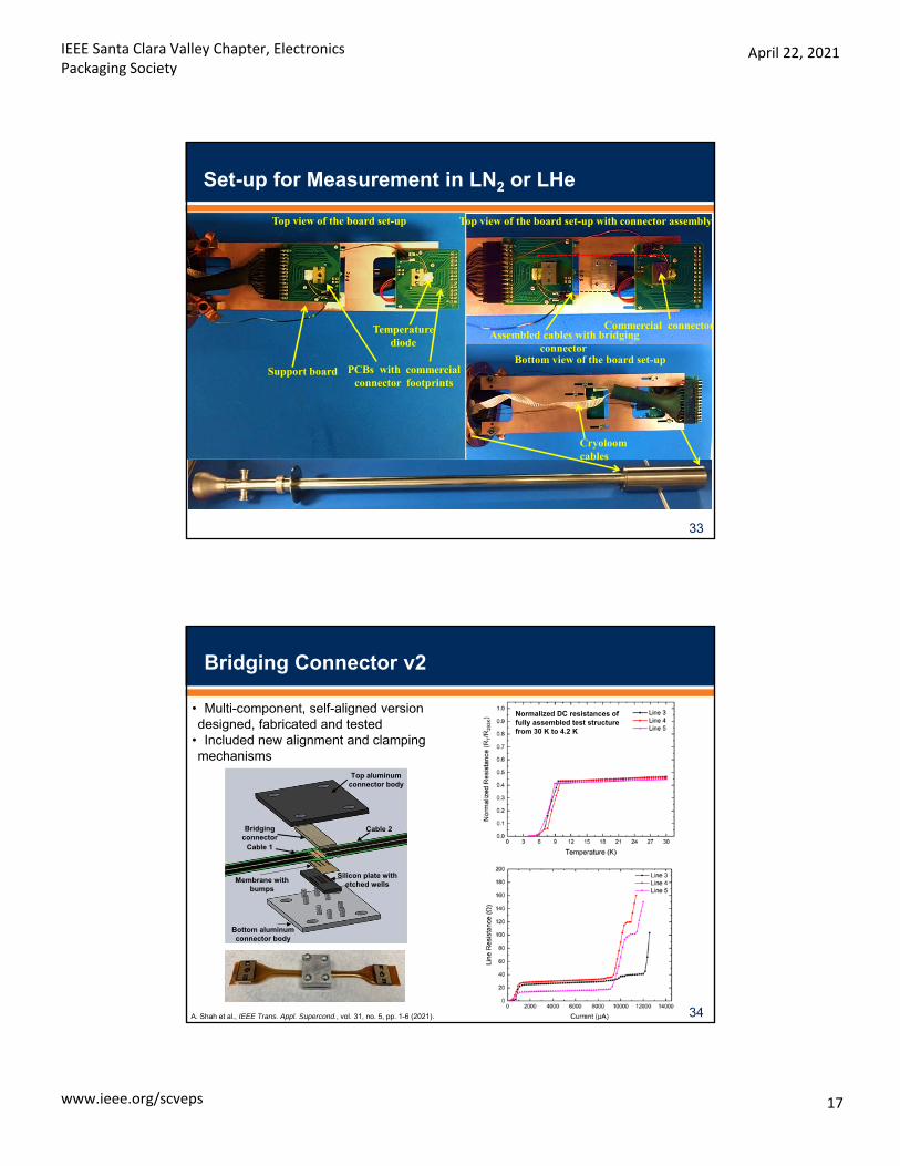
32
• Multi-component, self-aligned version designed, fabricated and tested
• Included new alignment and clamping mechanisms
A. Shah et al., IEEE Trans. Appl. Supercond., vol. 31, no. 5, pp. 1-6 (2021).
Bridging Connector v2
Laser released thin-film cable:• 12 parallel Nb signal lines• Pitch: 300 µm• HD 4100 as a protective layer
Bridging connector:• Stripline structure• Nb as the conductor• Polyimide HD-4110 as the dielectric
Polyimide membrane w/ Cu pillars:• Pillar height: 10 µm• Pillar Diameter: 100 µm
Si plate w/ wells on bottom Al body:• Well depth: 20 µm• Well diameter: 300 µm
Bottom aluminum connector body
Cable 1
Cable 2
Silicon plate with etched wells
Bridging connector
Membrane with bumps
Top aluminumconnector body
IEEE Santa Clara Valley Chapter, Electronics Packaging Society
April 22, 2021
www.ieee.org/scveps 17
Approach
33
Support board
Commercial connectorTemperature diode
PCBs with commercial connector footprints
Top view of the board set-up Top view of the board set-up with connector assembly
Bottom view of the board set-up
Assembled cables with bridging connector
Cryoloomcables
Set-up for Measurement in LN2 or LHe
Approach
34
• Multi-component, self-aligned version designed, fabricated and tested
• Included new alignment and clamping mechanisms
A. Shah et al., IEEE Trans. Appl. Supercond., vol. 31, no. 5, pp. 1-6 (2021).
Bridging Connector v2
Bottom aluminum connector body
Cable 1
Cable 2
Silicon plate with etched wells
Bridging connector
Membrane with bumps
Top aluminumconnector body
Normalized DC resistances of fully assembled test structure from 30 K to 4.2 K
IEEE Santa Clara Valley Chapter, Electronics Packaging Society
April 22, 2021
www.ieee.org/scveps 18
Approach
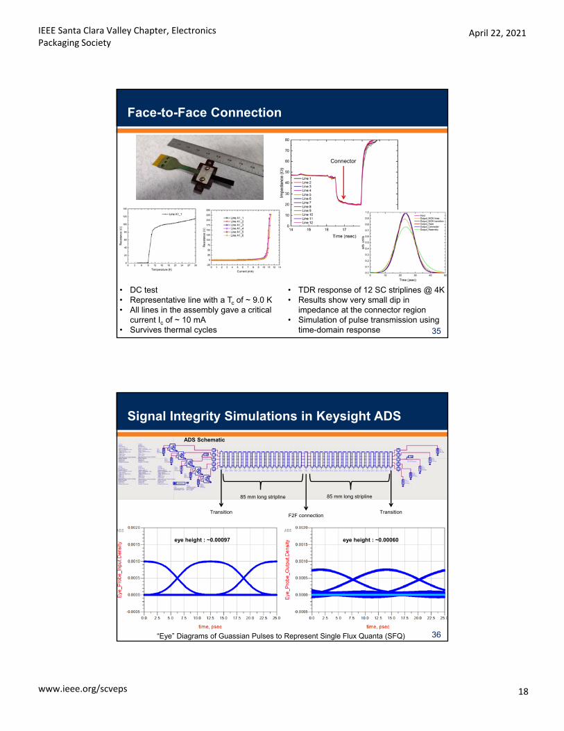
35
• DC test• Representative line with a Tc of ~ 9.0 K • All lines in the assembly gave a critical
current Ic of ~ 10 mA• Survives thermal cycles
• TDR response of 12 SC striplines @ 4K• Results show very small dip in
impedance at the connector region• Simulation of pulse transmission using
time-domain response
Connector
Face-to-Face Connection
Approach
36
Signal Integrity Simulations in Keysight ADS
85 mm long stripline 85 mm long stripline
F2F connectionTransition Transition
eye height : ~0.00097 eye height : ~0.00060
ADS Schematic
“Eye” Diagrams of Guassian Pulses to Represent Single Flux Quanta (SFQ)

IEEE Santa Clara Valley Chapter, Electronics Packaging Society
April 22, 2021
www.ieee.org/scveps 19
Approach
37
Additional Comments
• Other considerations:• Mechanical reliability (repetitive flexing, cooling in flexed
configuration, …)• Environmental stability (impact of humidity, barrier layers, …)• Thermal cycle reliability (fabrication at elevated temps, then use @ /
cycle to/from < 4 K, …)• Maintain positioning when cooled (fiber alignment, …)
• New packaging & integration technologies:• Alternative MCM substrates and construction (for better CTE match)• Suitable materials for die attach and underfill (re-workability?)• Connectors
Approach
38
Outline
• Intro Comments & Overview
• P&I for Cryogenic Electronics• Superconducting resonators• Interconnects (Superconducting Flex Cables)• Connectors (Cable-to-Cable)
• Moving towards Quantum• Very brief intro to “quantum”• Challenges• Approaches
• Concluding Comments

IEEE Santa Clara Valley Chapter, Electronics Packaging Society
April 22, 2021
www.ieee.org/scveps 20
Approach
39
Classical vs. Quantum
• Classical:
• Quantum:
0 or 1
|0⟩ and |1⟩
SwitchON or OFF
Capacitor / NodeCharged to V
Or Not Charged
Superposition& Entanglement
• Historically, many different device structures and materials systems were (are still being) explored
• Exponential growth once CMOS and materials were settled upon
• Si vs. other semi., clean SiO2, etc.• Continued materials advances to
support continued growth
• Many similarities (regarding technology & materials status)
• Currently, multiple different qubit types/structures and materials are being explored (with massive scaling in mind)
• Beginning (hoping) to see sustained growth (exponential?)
• Tremendous number of materials studies and advances are needed (expected)
|𝜓⟩ 𝛼|0⟩ 𝛽|1⟩
Bloch SphereRepresentation
https://www.quantum-inspire.com/kbase/bloch-sphere/
Approach
40
• Superconducting microwave qubits (cQED)
• Single microwave photon < 10 GHz (superconducting JJ-based circuit coupled to a superconducting cavity)
• Cooled to ~ 10 mK in dilution fridge
• Ion qubits:• Electronic states of trapped ions and
collective ion motion• Trapped, laser cooled
• Photonic / Optical qubits (Linear or Nonlinear Optical QC):
• Spin or orbital angular momentum components (modes) of photons
• Squeezed systems or cluster states
• …
A Few Examples of Qubit Approaches
IonQ
IBMGoogle
PsiQuantum

IEEE Santa Clara Valley Chapter, Electronics Packaging Society
April 22, 2021
www.ieee.org/scveps 21
Approach
41
• Quantum states are (usually) delicate:• Preserve coherence to maintain superposition / entanglement• Allow unitary operations to manipulate / interact qubits
• Trade-off between control and coherence.• “Control” includes manipulation, interaction, movement, measurement• Higher isolation from “environment”, longer coherence
• Visualize noise as smearing of location on Bloch sphere• Decoherence - destroys quantum information in qubit
• Can think of situation as quality factor of resonator:• Q’s of loss mechanisms sum as inverse (i.e., 1/Qa + 1/Qb + …) and overall Q
dominated by lowest Q process• (Or a bucket with water & holes)
• This is the situation we’re in now, exploring what and where the “holes” / loss processes are to reduce the leaks to a level acceptable for quantum error correction. ➞ Scaling!
Quantum Challenges
Approach
42
Quantum Packaging & Integration (Q-P&I)
• At least three phases for Q-P&I:I. Previous phase:
- Many different experimental and some small number of “operational” quantum computing / QIP systems
- < ~ 100 qubits, integrated onto one “chip” in one “package”
II. Current phase: “NISQ” or noise intermediate scale quantum1
- ~ 100 qubits, most likely still integrated onto/into one chip/package
- Increasing challenge to add comm/control/I/O electronics to external systems- Beginning to see those electronics move closer to the quantum hardware
- Quantum state transduction (QST) to (noisily) move Q info between systems
- Opportunity to deeply explore P&I materials and structures to learn about impact on quantumness (see recent Science article 2)
- Use qubits to sense the “defects”
III. Following phase(s) (post-NISQ):- > 103…106…and more, not necessarily on/in one chip/package- Incorporating quantum error correction (QEC) (move from physical to logical qubits)
- Need for quantum capable / transparent interfaces
- Need understanding of how materials & interfaces affect Q info (decoherence) and need ability to control / remove those effects
[1] Preskill, John. "Quantum Computing in the NISQ era and beyond." Quantum 2 (2018): 79.[2] de Leon et al. "Materials challenges and opportunities for quantum computing hardware." Science 372, no. 6539 (2021).

IEEE Santa Clara Valley Chapter, Electronics Packaging Society
April 22, 2021
www.ieee.org/scveps 22
Approach
43
• Superconducting microwave qubits:• 5 GHz photon: 20 eV• Thermal noise @ RT (290 K): 25,000 eV ~ -174 dBm/Hz• Thermal noise @ 4 K: 345 eV ~ -193 dBm/Hz• Thermal noise @ 10 mK: 0.9 eV ~ -219 dBm/Hz
• Potentially millions of interconnects*, with high density
• Impedance matching: not necessarily 50 systems, no reflections
• Control crosstalk and scattering (resonance/mode control in packages)
• High thermal isolation, reduced thermal load, thermalization, attenuation
• Reliability and stability (thermal-cycle)
• Need to eliminate loss into unknown or unclear loss processes through interaction with states in dielectrics (two level system, or TLS), such as surface oxidation or interface states…difficult to passivate.
Q-P&I Challenges for Superconducting Qubits
* Bardin, IEEE MTT-S Webinar, April 13th, 2021.
Approach
44
Nb Microstrip Resonators on PI and HD @ 20 mK
From University of Sydney (Reilly Group)
Our sample
Frequency (GHz)
Tra
nsm
issi
on (
dB)
Power (dBm)
Qua
lity
Fac
tor
Frequency (GHz)
Tra
nsm
issi
on (
dB)
-30
-40
-50
-30
-40
-50
2.020 2.0222.021
-60
1.9676 1.9684
5
20
15
10
-40-60-80-100
1st harmonic
4th3rd2nd
(a)
(c)
(b)
-36 dBm
-56-46-41
x 103
0
-40 dBm
D. B. Tuckerman et al., Supercond. Sci. Technol. 29 084007 (2016).

IEEE Santa Clara Valley Chapter, Electronics Packaging Society
April 22, 2021
www.ieee.org/scveps 23
Approach
45
Loss at Low Microwave Power (Low ⟨nphoton⟩ )
Power (dBm)
Qua
lity
Fac
tor
5
20
15
10
-40-60-80-100
1st harmonic
4th3rd2nd
(a) x 103
0
D. B. Tuckerman et al., Supercond. Sci. Technol. 29084007 (2016).
Sage et al., Journal of Applied Physics 109, no. 6 (2011): 063915.
Megrant et al., Applied Physics Letters 100, no. 11 (2012): 113510.
Grünhaupt et al., Physical review letters 121, no. 11 (2018): 117001.
Approach
46
Active Area of Research (Small Sample)
Lienhard et al., "Microwave Packaging for Superconducting Qubits," 2019 IEEE MTT-S International Microwave Symposium (IMS).
Bronn et al., “High coherence plane breaking packaging for superconducting qubits” 2018 Quantum Sci. Technol. 3 024007
Intel’s Tangle Lake SC quantum processor: 49 qubits & 108 RF connections to the outside world.
Intel’s 3 Si spin qubit chip, defined by 7 gates. Ratio of control wires to qubits is >>1.
J. S. Clarke, "Quantum Computing and the Importance of Interconnects," 2018 IEEE IITC.
Multi-layer In interconnects (stacked-chips)
Foxen et al., “Qubit compatible superconducting interconnects”, Quantum Science and Technology, 3(1), 014005 (2017). Lei et al., "High coherence superconducting microwave cavities with
indium bump bonding." Applied Physics Letters 116.15 (2020): 154002.
Package Design & Construction

IEEE Santa Clara Valley Chapter, Electronics Packaging Society
April 22, 2021
www.ieee.org/scveps 24
Approach
47
Closing Comments
• Packaging & integration for cryogenic electronics• Growing number of applications (space, quantum, etc.)• SC resonators for materials exploration• Various types of superconducting flexible cables with very high
performance (ultra-low loss, low cross-sections)• Multiple types of connectors with suitable performance, but still room
for improvement
• Moving towards quantum systems• Many opportunities for materials and P&I structure exploration• + many challenges
• Thank You!