P3HT:PCBM Bulk-Heterojunctions: Observing Interfacial and ...
9
P3HT:PCBM Bulk-Heterojunctions: Observing Interfacial and Charge Transfer States with Surface Photovoltage Spectroscopy Frank E. Osterloh,* ,† Michael A. Holmes, † Jing Zhao, † Lilian Chang, ‡ Steven Kawula, ‡ John D. Roehling, ‡ and Adam J. Moule ́ ‡ † Department of Chemistry, and ‡ Department of Chemical Engineering and Materials Science, University of California, One Shields Avenue, Davis, California 95616, United States * S Supporting Information ABSTRACT: Surface photovoltage (SPV) spectra are reported for separate films of (6,6)-phenyl-C 61 -butyric acid methyl ester (PCBM) and for regioregular and regiorandom poly(3-hexylthiophene) (P3HT):PCBM bulk heterojunctions, as a function of wavelength, film thickness, thermal annealing, and substrate. In PCBM films, two photovoltage features are observed at 1.1−1.4 eV (F1) and 1.4−2.3 eV (F2), which are assigned to excitation of charge transfer states at the interface (F1) and in the bulk (F2) of the film. In BHJ films, five different photovoltage features are observed at 0.75−0.9 eV (F1), 0.9−1.3 eV (F2), 1.3−1.8 eV (F3), 1.8−2.0 eV (F4), and 2.0−2.4 eV (F5). This data can be analyzed on the basis of optical absorbance and fluorescence spectra of the films, and using SPV spectra for PCBM and P3HT only films, and for a BHJ film containing P3HT nanofibers for comparison. SPV features are assigned to states at the polymer−substrate interface (F1 and F2), the P3HT:PCBM charge transfer state (F3), the self-ionized (CT) state of P3HT (F4), and the band gap transition of P3HT (F5). This interpretation is also consistent with molecular orbital energy diagrams and electron microscopy-derived topological maps of the films. Photovoltage sign and substrate dependence can be understood with the depleted semiconductor model. Features F1−4 are caused by polarization of electrostatically bound charge pairs by the built-in electric field at the substrate−BHJ interface, whereas F5 is due to transport of free charge carriers through the film and through the substrate film interface. This work will promote the understanding of photochemical charge generation and transport in organic photovoltaic films. ■ INTRODUCTION Since its initial discovery in 1992 by Hiramoto, 1 the bulk heterojunction (BHJ) organic photovoltaic (OPV) device has been continuously improved. 2−7 The large interface in BHJs maximizes contact between the organic semiconductors and enhances charge separation of the relatively short-lived exciton pairs. 8−11 Charge separation is mediated by so-called transfer (CT) states that form as a result of the electronic interactions between P3HT and PCBM. The excitation energies of these states are below the band gap of the component materials, and they determine the maximum open circuit voltage (V oc ) of the solar cell. 12 In optical absorption spectra CT states are difficult to observe due to their low absorption cross section, but they have been detected using other more sensitive techni- ques. 8,13−17 Additional midgap states at the polymer−electrode interfaces can result from chemical reactions with oxygen or from adsorption of solvent molecules. 18−21 Such states have been observed with ultraviolet photoemission spectroscopy and inverse photoemission spectroscopy. 22−25 They can affect photocurrent by trapping charge carriers or by inducing electric fields. 26−30 We recently applied surface photovoltage spectros- copy (SPS) for the detection of CT and interface states in films of regioregular P3HT. 31 SPS uses a semitransparent Kelvin probe that contactlessly probes the surface potential change of an illuminated film (Figure 1) versus the excitation energy. 32,33 Measurable signals can be due to motion of free charge carriers through the film or the interface, due to polarization of charge Received: January 8, 2014 Revised: June 5, 2014 Published: June 6, 2014 Figure 1. Geometry of SPV measurement and example spectra. Contact potential changes are generated by polarization (POL) or electron/hole transfer (ET/HT) into the substrate. A negative ΔCPD signal corresponds to electron movement toward the substrate. The ΔCPD value can be interpreted as the voltage that develops between the film and the substrate under illumination. Article pubs.acs.org/JPCC © 2014 American Chemical Society 14723 dx.doi.org/10.1021/jp500226u | J. Phys. Chem. C 2014, 118, 14723−14731
Transcript of P3HT:PCBM Bulk-Heterojunctions: Observing Interfacial and ...

P3HT:PCBM Bulk-Heterojunctions: Observing Interfacial and ChargeTransfer States with Surface Photovoltage SpectroscopyFrank E. Osterloh,*,† Michael A. Holmes,† Jing Zhao,† Lilian Chang,‡ Steven Kawula,‡ John D. Roehling,‡
and Adam J. Moule ‡
†Department of Chemistry, and ‡Department of Chemical Engineering and Materials Science, University of California, One ShieldsAvenue, Davis, California 95616, United States
*S Supporting Information
ABSTRACT: Surface photovoltage (SPV) spectra are reported for separatefilms of (6,6)-phenyl-C61-butyric acid methyl ester (PCBM) and forregioregular and regiorandom poly(3-hexylthiophene) (P3HT):PCBM bulkheterojunctions, as a function of wavelength, film thickness, thermalannealing, and substrate. In PCBM films, two photovoltage features areobserved at 1.1−1.4 eV (F1) and 1.4−2.3 eV (F2), which are assigned toexcitation of charge transfer states at the interface (F1) and in the bulk (F2)of the film. In BHJ films, five different photovoltage features are observed at0.75−0.9 eV (F1), 0.9−1.3 eV (F2), 1.3−1.8 eV (F3), 1.8−2.0 eV (F4), and2.0−2.4 eV (F5). This data can be analyzed on the basis of opticalabsorbance and fluorescence spectra of the films, and using SPV spectra forPCBM and P3HT only films, and for a BHJ film containing P3HTnanofibers for comparison. SPV features are assigned to states at thepolymer−substrate interface (F1 and F2), the P3HT:PCBM charge transfer state (F3), the self-ionized (CT) state of P3HT(F4), and the band gap transition of P3HT (F5). This interpretation is also consistent with molecular orbital energy diagramsand electron microscopy-derived topological maps of the films. Photovoltage sign and substrate dependence can be understoodwith the depleted semiconductor model. Features F1−4 are caused by polarization of electrostatically bound charge pairs by thebuilt-in electric field at the substrate−BHJ interface, whereas F5 is due to transport of free charge carriers through the film andthrough the substrate film interface. This work will promote the understanding of photochemical charge generation and transportin organic photovoltaic films.
■ INTRODUCTION
Since its initial discovery in 1992 by Hiramoto,1 the bulkheterojunction (BHJ) organic photovoltaic (OPV) device hasbeen continuously improved.2−7 The large interface in BHJsmaximizes contact between the organic semiconductors andenhances charge separation of the relatively short-lived excitonpairs.8−11 Charge separation is mediated by so-called transfer(CT) states that form as a result of the electronic interactionsbetween P3HT and PCBM. The excitation energies of thesestates are below the band gap of the component materials, andthey determine the maximum open circuit voltage (Voc) of thesolar cell.12 In optical absorption spectra CT states are difficultto observe due to their low absorption cross section, but theyhave been detected using other more sensitive techni-ques.8,13−17 Additional midgap states at the polymer−electrodeinterfaces can result from chemical reactions with oxygen orfrom adsorption of solvent molecules.18−21 Such states havebeen observed with ultraviolet photoemission spectroscopy andinverse photoemission spectroscopy.22−25 They can affectphotocurrent by trapping charge carriers or by inducing electricfields.26−30 We recently applied surface photovoltage spectros-copy (SPS) for the detection of CT and interface states in filmsof regioregular P3HT.31 SPS uses a semitransparent Kelvin
probe that contactlessly probes the surface potential change ofan illuminated film (Figure 1) versus the excitation energy.32,33
Measurable signals can be due to motion of free charge carriersthrough the film or the interface, due to polarization of charge
Received: January 8, 2014Revised: June 5, 2014Published: June 6, 2014
Figure 1. Geometry of SPV measurement and example spectra.Contact potential changes are generated by polarization (POL) orelectron/hole transfer (ET/HT) into the substrate. A negative ΔCPDsignal corresponds to electron movement toward the substrate. TheΔCPD value can be interpreted as the voltage that develops betweenthe film and the substrate under illumination.
Article
pubs.acs.org/JPCC
© 2014 American Chemical Society 14723 dx.doi.org/10.1021/jp500226u | J. Phys. Chem. C 2014, 118, 14723−14731

carrier pairs (polarons) or due to the injection of charge carriersinto molecular adsorbates.34 Since the technique is potential-sensitive and not based on photocurrents, even low densities ofstates and their excitation energies can be observed.34−39
Here we use the technique on films of (6,6)-phenyl-C61-butyric acid methyl ester (PCBM),10,40−43 and on bulkheterojunction films formed by self-assembly of PCBM andthe polymer poly(3-hexylthiophene) (P3HT). SPV spectrawere recorded as a function of substrate material, film annealingconditions, and film thickness, and using amorphous TiOx andcalcium niobate interlayers.44 Five photovoltage features weredetected that can be assigned to interface states, to electronictransitions of P3HT, and to the P3HT:PCBM charge transferstate. Within the PCBM films, two low-energy opticaltransitions can be assigned to interfacial states and directexcitation of PCBM. The size and sign of the low-energyphotovoltage features agree with the depleted semiconductormodel, while the high-energy feature can be explained bydiffusive charge transport.
■ EXPERIMENTAL DETAILSSample Preparation. Poly-3-hexylthiophene (P3HT) with
M.W. ≈75 kDa and a reported regioregularity of ≥95% wasobtained from Plextronics. (6,6)-Phenyl-C61-butyric acidmethyl ester (PCBM) was purchased from Nano-C. Theaqueous suspension of PEDOT:PSS (Clevios P VP Al 4083)with resistivity between 500 and 5000 Ω cm was filtered withan 0.45 μm Teflon filter before coating. Tetrabutylammonium-capped calcium niobate nanosheets (CNO) were preparedaccording to published procedures.45,46 Before depositing, thenanosheets were centrifuged and redispersed three times inabsolute ethanol and four times in deionized 18 MΩ water. ATiOx sol−gel was synthesized from titanium isopropoxide(TIP, 97%, Sigma-Aldrich) according to published procedure47
and diluted in methanol for spin-coating. Polymer films wereprepared by first dissolving P3HT and PCBM in chlorobenzene(20 mg/mL) and heating at 60 °C overnight. An 80 ± 5 nmthick film of 1:1 P3HT:PCBM BHJ (PCBM-only, 60 ± 5 nmthick) was prepared by spin-coating in an inert nitrogenatmosphere onto a 1.0 in.2 commercial-grade indium−tin oxide(ITO) coated glass slide. Thicker BHJ films (250 ± 20 nm)were prepared with the same procedure using twice theconcentration (40 mg/mL) and spinning at 50% reducedspeed. Nanofiber BHJ films were prepared by spin coating atoluene solution of 1:1 PCBM and PH3T J-aggregatenanofibers (the latter prepared separately using the knownprocedure48) at a speed of 600 rpm. The nanofibers wereseveral micrometers in length and 15 nm in diameter. The ITO(ca. 140 nm thick and 15 Ω sheet resistance) was cleanedbefore use by ultrasonicating for 10 min in acetone, 2-propanol,and then water, respectively. Immediately before use the ITOwas exposed to UV-ozone for 30 min and then transferreddirectly to inert atmosphere for deposition. Silver-coated glasssubstrates (100 nm) were prepared in-house through vapordeposition. When indicated, an interlayer of PEDOT:PSS (40nm) or CNO (15 nm) or TiOx (20 nm) were spin-coated ontothe ITO substrate and heated at 110−150 °C for 5 min toremove any remaining solvent before depositing the BHJ layer.To test the effect of heat treatment, sample annealing wasperformed at 110 °C for 15 min under nitrogen atmosphere.Measurements. UV−vis absorption spectra were recorded
with a Thermo Scientific Evolution 220 UV−vis spectropho-tometer equipped with an integrating sphere. Film thicknesses
were measured with a Dektak surface profiler calibrated to aSi−SiO2 ellipsometry standard. Monochromatic light intensitymeasurements were performed using an International LightTechnologies IL400BL photometer with an IR-visible detector.SPV measurements were conducted inside a custom-built high-vacuum measurement chamber connected to a Pfeiffer HiCube80 Eco turbo pump and a Besocke Delta Phi GmbH Kelvinprobe control unit. Contact potential difference (CPD) signalswere measured using a vibrating Kelvin probe (Au grid, 3 mmdiameter, 60% transparent) and read out with a Keithley 2700voltmeter that was connected to a PC. Light was generated by175 W Xe arc lamp and filtered through a monochromator(Oriel Cornerstone 130). The light power density at the samplewas <1 mW cm−2. Note that our previously reported photofluxvalues were incorrect.31 The x-axis values in Figure 7B inreference 31 should be by a factor of 109 smaller. The correct x-axis value range is 1×10¹⁴−1×10¹⁷. Film samples were mountedinside the vacuum chamber, 1.0 mm underneath the Kelvinprobe, the chamber was evacuated to 10−7 bar, and spectra wereobtained by scanning from low to high energy in 100 cm−1
steps with a period interval of 5 s. Light spectra were correctedfor background effects (drift, desorption of gas and solventmolecules) by subtracting a prior background scan conductedin the dark. The spectra plot the contact potential difference(CPD) signal versus photon energy. The CPD value is thedifference in work functions between the sample film and thegold Kelvin probe, plus contributions from surface and interfacedipoles.31,33 A positive CPD change corresponds to aphotodipole with a negative pole at the surface and the positiveside toward the back electrode. High-angle annular dark-fieldelectron tomography (HAADF-ET) data were acquired with anJEOL 2100F electron microscope at 200 kV. Reconstructionswere performed using custom code in MATLAB (MathWorks)utilizing the DART algorithm. The reconstruction minimizedthe difference between the forward-projected reconstructionand the original tilt series, yielding a material-labeledreconstruction that closely matched the original data. A two-dimensional vertical slice of the original 3D data is presented inFigure 5 (viewing a small cross section of a BHJ).
■ RESULTS AND DISCUSSIONFigure 2A shows optical absorption and SPV spectra of apristine PCBM film deposited onto ITO.The optical spectrum is similar to other literature reports for
PCBM49 and C60 films.50 The absorption edge at 1.75 eV has
been previously assigned to charge transfer (CT) states formedby the interaction between fullerenes within the film.29,49,51−54
With thick films, a weak absorption tail out to 1.55 eV can beseen.49 The small sharp 1.75 eV absorption is due to theformation of a “Frenkel exciton” (electron hole pair within thesame fullerene).29,49 The direct excitation of this state isforbidden by the selection rules of the icosahedral fullerene,55,56
but emission from this state can be observed in photo-luminescence spectra of PCBM.49 The SPV spectrum of thePCBM film contains a negative feature at 1.1−1.4 eV and apositive one at 1.4−2.3 eV. The fine structure of feature 1 (F1)is caused by the specific emission lines of the Xe arc lamp, asdetailed in our earlier paper.31 Because of its low intensity andlow excitation energy, F1 is assigned to interface charge transfer(ICT) states at the PCBM−substrate interface. As the diagramin Figure 2B shows, the PCBM HOMO and the ITOconduction band edges have a 1.3 eV band offset in the regionof the photovoltage signal. Excitation of these states would
The Journal of Physical Chemistry C Article
dx.doi.org/10.1021/jp500226u | J. Phys. Chem. C 2014, 118, 14723−1473114724
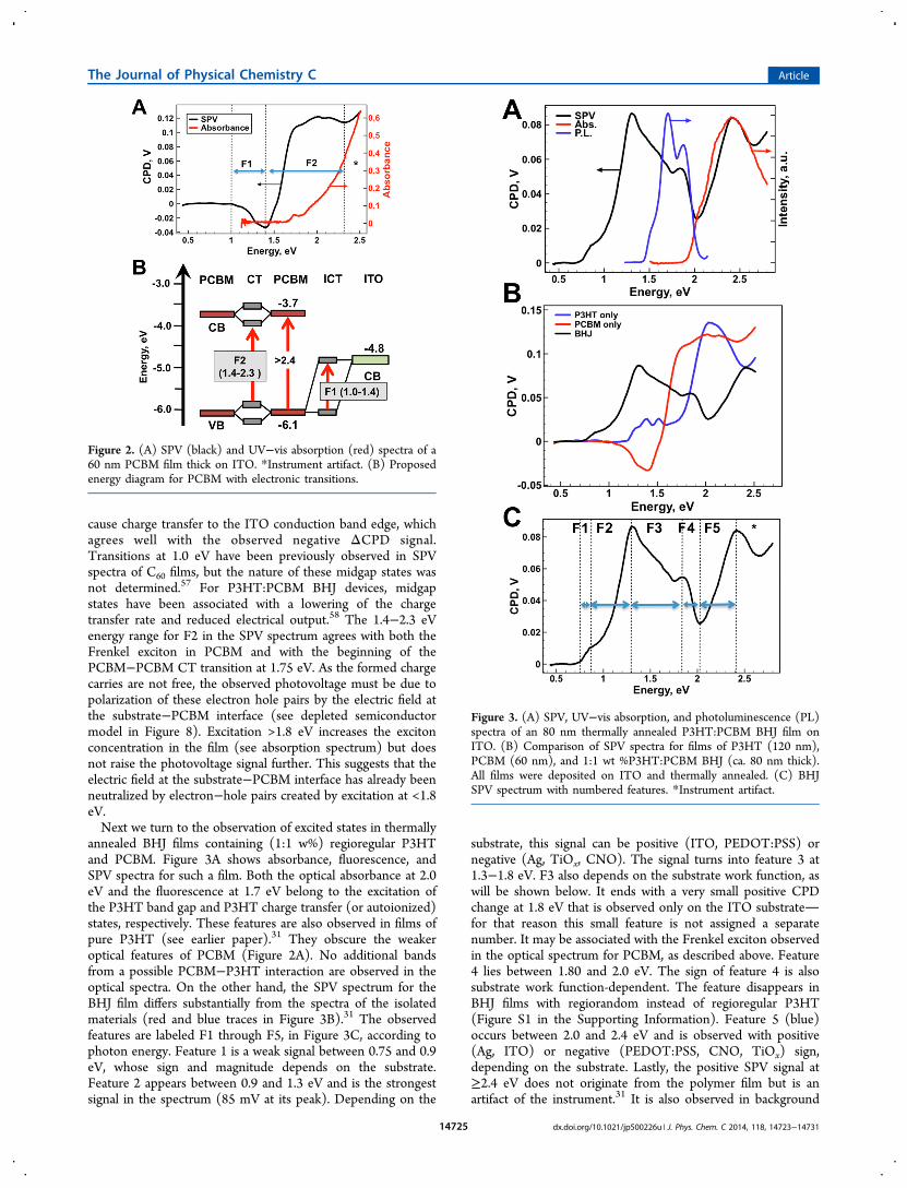
cause charge transfer to the ITO conduction band edge, whichagrees well with the observed negative ΔCPD signal.Transitions at 1.0 eV have been previously observed in SPVspectra of C60 films, but the nature of these midgap states wasnot determined.57 For P3HT:PCBM BHJ devices, midgapstates have been associated with a lowering of the chargetransfer rate and reduced electrical output.58 The 1.4−2.3 eVenergy range for F2 in the SPV spectrum agrees with both theFrenkel exciton in PCBM and with the beginning of thePCBM−PCBM CT transition at 1.75 eV. As the formed chargecarries are not free, the observed photovoltage must be due topolarization of these electron hole pairs by the electric field atthe substrate−PCBM interface (see depleted semiconductormodel in Figure 8). Excitation >1.8 eV increases the excitonconcentration in the film (see absorption spectrum) but doesnot raise the photovoltage signal further. This suggests that theelectric field at the substrate−PCBM interface has already beenneutralized by electron−hole pairs created by excitation at <1.8eV.Next we turn to the observation of excited states in thermally
annealed BHJ films containing (1:1 w%) regioregular P3HTand PCBM. Figure 3A shows absorbance, fluorescence, andSPV spectra for such a film. Both the optical absorbance at 2.0eV and the fluorescence at 1.7 eV belong to the excitation ofthe P3HT band gap and P3HT charge transfer (or autoionized)states, respectively. These features are also observed in films ofpure P3HT (see earlier paper).31 They obscure the weakeroptical features of PCBM (Figure 2A). No additional bandsfrom a possible PCBM−P3HT interaction are observed in theoptical spectra. On the other hand, the SPV spectrum for theBHJ film differs substantially from the spectra of the isolatedmaterials (red and blue traces in Figure 3B).31 The observedfeatures are labeled F1 through F5, in Figure 3C, according tophoton energy. Feature 1 is a weak signal between 0.75 and 0.9eV, whose sign and magnitude depends on the substrate.Feature 2 appears between 0.9 and 1.3 eV and is the strongestsignal in the spectrum (85 mV at its peak). Depending on the
substrate, this signal can be positive (ITO, PEDOT:PSS) ornegative (Ag, TiOx, CNO). The signal turns into feature 3 at1.3−1.8 eV. F3 also depends on the substrate work function, aswill be shown below. It ends with a very small positive CPDchange at 1.8 eV that is observed only on the ITO substratefor that reason this small feature is not assigned a separatenumber. It may be associated with the Frenkel exciton observedin the optical spectrum for PCBM, as described above. Feature4 lies between 1.80 and 2.0 eV. The sign of feature 4 is alsosubstrate work function-dependent. The feature disappears inBHJ films with regiorandom instead of regioregular P3HT(Figure S1 in the Supporting Information). Feature 5 (blue)occurs between 2.0 and 2.4 eV and is observed with positive(Ag, ITO) or negative (PEDOT:PSS, CNO, TiOx) sign,depending on the substrate. Lastly, the positive SPV signal at≥2.4 eV does not originate from the polymer film but is anartifact of the instrument.31 It is also observed in background
Figure 2. (A) SPV (black) and UV−vis absorption (red) spectra of a60 nm PCBM film thick on ITO. *Instrument artifact. (B) Proposedenergy diagram for PCBM with electronic transitions.
Figure 3. (A) SPV, UV−vis absorption, and photoluminescence (PL)spectra of an 80 nm thermally annealed P3HT:PCBM BHJ film onITO. (B) Comparison of SPV spectra for films of P3HT (120 nm),PCBM (60 nm), and 1:1 wt %P3HT:PCBM BHJ (ca. 80 nm thick).All films were deposited on ITO and thermally annealed. (C) BHJSPV spectrum with numbered features. *Instrument artifact.
The Journal of Physical Chemistry C Article
dx.doi.org/10.1021/jp500226u | J. Phys. Chem. C 2014, 118, 14723−1473114725
spectra on non-coated substrates and will not be discussedfurther.Based on their excitation energy, F1−F5 can be assigned to
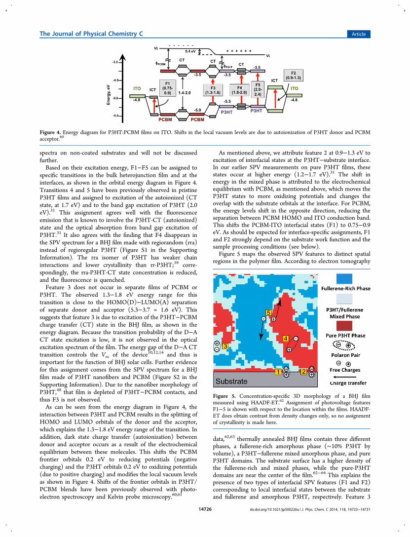
specific transitions in the bulk heterojunction film and at theinterfaces, as shown in the orbital energy diagram in Figure 4.Transitions 4 and 5 have been previously observed in pristineP3HT films and assigned to excitation of the autoionized (CTstate, at 1.7 eV) and to the band gap excitation of P3HT (2.0eV).31 This assignment agrees well with the fluorescenceemission that is known to involve the P3HT-CT (autoionized)state and the optical absorption from band gap excitation ofP3HT.31 It also agrees with the finding that F4 disappears inthe SPV spectrum for a BHJ film made with regiorandom (rra)instead of regioregular P3HT (Figure S1 in the SupportingInformation). The rra isomer of P3HT has weaker chaininteractions and lower crystallinity than rr-P3HT;59 corre-spondingly, the rra-P3HT-CT state concentration is reduced,and the fluorescence is quenched.Feature 3 does not occur in separate films of PCBM or
P3HT. The observed 1.3−1.8 eV energy range for thistransition is close to the HOMO(D)−LUMO(A) separationof separate donor and acceptor (5.3−3.7 = 1.6 eV). Thissuggests that feature 3 is due to excitation of the P3HT−PCBMcharge transfer (CT) state in the BHJ film, as shown in theenergy diagram. Because the transition probability of the D−ACT state excitation is low, it is not observed in the opticalexcitation spectrum of the film. The energy gap of the D−A CTtransition controls the Voc of the device10,12,14 and thus isimportant for the function of BHJ solar cells. Further evidencefor this assignment comes from the SPV spectrum for a BHJfilm made of P3HT nanofibers and PCBM (Figure S2 in theSupporting Information). Due to the nanofiber morphology ofP3HT,48 that film is depleted of P3HT−PCBM contacts, andthus F3 is not observed.As can be seen from the energy diagram in Figure 4, the
interaction between P3HT and PCBM results in the splitting ofHOMO and LUMO orbitals of the donor and the acceptor,which explains the 1.3−1.8 eV energy range of the transition. Inaddition, dark state charge transfer (autoionization) betweendonor and acceptor occurs as a result of the electrochemicalequilibrium between these molecules. This shifts the PCBMfrontier orbitals 0.2 eV to reducing potentials (negativecharging) and the P3HT orbitals 0.2 eV to oxidizing potentials(due to positive charging) and modifies the local vacuum levelsas shown in Figure 4. Shifts of the frontier orbitals in P3HT/PCBM blends have been previously observed with photo-electron spectroscopy and Kelvin probe microscopy.60,61
As mentioned above, we attribute feature 2 at 0.9−1.3 eV toexcitation of interfacial states at the P3HT−substrate interface.In our earlier SPV measurements on pure P3HT films, thesestates occur at higher energy (1.2−1.7 eV).31 The shift inenergy in the mixed phase is attributed to the electrochemicalequilibrium with PCBM, as mentioned above, which moves theP3HT states to more oxidizing potentials and changes theoverlap with the substrate orbitals at the interface. For PCBM,the energy levels shift in the opposite direction, reducing theseparation between PCBM HOMO and ITO conduction band.This shifts the PCBM-ITO interfacial states (F1) to 0.75−0.9eV. As should be expected for interface-specific assignments, F1and F2 strongly depend on the substrate work function and thesample processing conditions (see below).Figure 5 maps the observed SPV features to distinct spatial
regions in the polymer film. According to electron tomography
data,62,63 thermally annealed BHJ films contain three differentphases, a fullerene-rich amorphous phase (∼10% P3HT byvolume), a P3HT−fullerene mixed amorphous phase, and pureP3HT domains. The substrate surface has a higher density ofthe fullerene-rich and mixed phases, while the pure-P3HTdomains are near the center of the film.62−64 This explains thepresence of two types of interfacial SPV features (F1 and F2)corresponding to local interfacial states between the substrateand fullerene and amorphous P3HT, respectively. Feature 3
Figure 4. Energy diagram for P3HT:PCBM films on ITO. Shifts in the local vacuum levels are due to autoionization of P3HT donor and PCBMacceptor.60
Figure 5. Concentration-specific 3D morphology of a BHJ filmmeasured using HAADF-ET.62 Assignment of photovoltage featuresF1−5 is shown with respect to the location within the films. HAADF-ET does obtain contrast from density changes only, so no assignmentof crystallinity is made here.
The Journal of Physical Chemistry C Article
dx.doi.org/10.1021/jp500226u | J. Phys. Chem. C 2014, 118, 14723−1473114726

occurs in the fullerene−P3HT mixed phase, which isdominated by CT interactions between P3HT and PCBM.63
This phase is reduced in the nanofiber P3HT/PCBM blend(Figure S2 in the Supporting Information), and correspond-ingly, F3 is not observed there. Feature 4 is expected to be mostprominent in the crystalline regions of pure-P3HT domainswhere the concentration of P3HT CT states is highest. Finally,F5 (2.0−2.4 eV) involves band gap excitation of P3HTfollowed by the formation of free and mobile charges. Thesignal is associated with excitation of ordered P3HT domainsand then of amorphous P3HT or PCBM at higher excitationenergy.Having assigned all photovoltage features to energy states
and locations in the film, we next examine the substratedependence of the SPV spectra. As can be seen from Figure 6,
size and direction of all features in the spectrum are influencedby the substrate. The most significant changes are the inversionof F2 in going from the ITO substrate (Figure 3A) to CNO-coated silver (Figure 6C) and the inversion of F5 in going fromsilver (Figure 6A) to PEDOT:PSS coated ITO (Figure 6B).Also, F1 and F3 disappear on the silver substrate (Figure 6A).In order to understand these spectral variations and their
dependence on the substrate, all photovoltage signals wereplotted in Figure 7 against the substrate work function.
Features 1 and 2, and to some extent, F3, show a monotonicincrease with the work function of the substrate. In contrast,features 4 and 5 exhibit no clear trend. These observations canbe rationalized with the depleted semiconductor model in Figure8. According to this model, charge carriers in the excited BHJfilm move under a built-in electric field that results from theelectrochemical equilibrium at the substrate−polymer interfaceand from (unknown) dipoles at the interface.31,33,65−68 Thebuilt-in field derives from the potential drop Vbi within thespace charge layer of the film. The potential drop originatesfrom the initial difference of Fermi levels in substrate EF(Sub)and polymer film EF(BHJ) before electrical contact is made:eVbi = EF(Sub) − EF(BHJ). Based on the inversion of thepolarity of the F2 signal in Figure 7, the Fermi level EF of thepolymer can be estimated as −4.7 eV, slightly above the EF ofITO (−4.8 eV). The depleted semiconductor model issupported by impedance spectroscopy,69,70 capacitance meas-urements,28,71 and time-of-flight electron-collection.72 Further-more, XPS and UPS studies also confirm an electrochemicalequilibrium between P3HT:PCBM and substrate.25,26,30,73,74 Inthese earlier studies, the polymer film was observed to be mildlyp-type, as a result of exposure to oxygen and water during filmpreparation. On the contrary, the films described here areclearly mildly n-type, on the basis of the SPV data and themodel in Figure 8. This is due to the exclusion of oxygen duringthe SPV measurements and during film preparation (seeExperimental section).According to Figure 8, the surface photovoltage in the
P3HT:PCBM film is generated by polarization of electrostati-cally coupled electron−hole pairs under the built-in field (F1−4) or by transfer of free charge carriers through the film andacross the polymer−substrate interface (F5). Because F1 andF2 are excited first during the monochromatic scan, they aremost strongly controlled by the built-in field. However, asincreasing concentrations of charge carriers build up andpolarize the film, the interfacial electric field is attenuated, andthe driving force for charge separation at higher energyexcitation is diminished. As a result, F3 and F4 are less
Figure 6. SPV spectra of P3HT:PCBM BHJ films (ca. 80 nm thick,annealed at 110 °C for 15 min) on various substrates: (A) silver; (B)PEDOT:PSS deposited on ITO; (C) colloidal TiOx and CNOdeposited on Ag.
Figure 7. Photovoltage variation with substrate work function for aP3HT:PCBM BHJ film: (a) from Lide et al;75 (b) from Chang et al;44
(c) from Xu et al.76 A linear relationship between ΔCPD and thesubstrate work function would be expected if charge transfer wasdriven by the built-in potential of the substrate−polymer junction. F1and F2 approach this situation.
The Journal of Physical Chemistry C Article
dx.doi.org/10.1021/jp500226u | J. Phys. Chem. C 2014, 118, 14723−1473114727
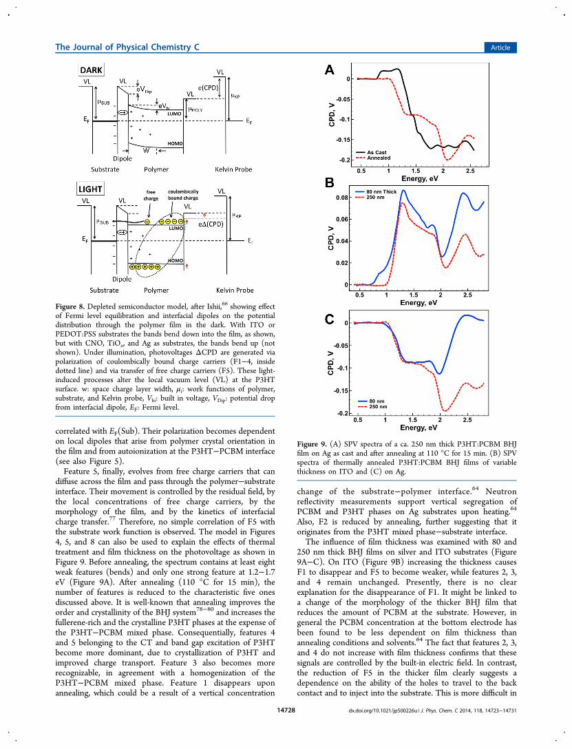
correlated with EF(Sub). Their polarization becomes dependenton local dipoles that arise from polymer crystal orientation inthe film and from autoionization at the P3HT−PCBM interface(see also Figure 5).Feature 5, finally, evolves from free charge carriers that can
diffuse across the film and pass through the polymer−substrateinterface. Their movement is controlled by the residual field, bythe local concentrations of free charge carriers, by themorphology of the film, and by the kinetics of interfacialcharge transfer.77 Therefore, no simple correlation of F5 withthe substrate work function is observed. The model in Figures4, 5, and 8 can also be used to explain the effects of thermaltreatment and film thickness on the photovoltage as shown inFigure 9. Before annealing, the spectrum contains at least eightweak features (bends) and only one strong feature at 1.2−1.7eV (Figure 9A). After annealing (110 °C for 15 min), thenumber of features is reduced to the characteristic five onesdiscussed above. It is well-known that annealing improves theorder and crystallinity of the BHJ system78−80 and increases thefullerene-rich and the crystalline P3HT phases at the expense ofthe P3HT−PCBM mixed phase. Consequentially, features 4and 5 belonging to the CT and band gap excitation of P3HTbecome more dominant, due to crystallization of P3HT andimproved charge transport. Feature 3 also becomes morerecognizable, in agreement with a homogenization of theP3HT−PCBM mixed phase. Feature 1 disappears uponannealing, which could be a result of a vertical concentration
change of the substrate−polymer interface.64 Neutronreflectivity measurements support vertical segregation ofPCBM and P3HT phases on Ag substrates upon heating.64
Also, F2 is reduced by annealing, further suggesting that itoriginates from the P3HT mixed phase−substrate interface.The influence of film thickness was examined with 80 and
250 nm thick BHJ films on silver and ITO substrates (Figure9A−C). On ITO (Figure 9B) increasing the thickness causesF1 to disappear and F5 to become weaker, while features 2, 3,and 4 remain unchanged. Presently, there is no clearexplanation for the disappearance of F1. It might be linked toa change of the morphology of the thicker BHJ film thatreduces the amount of PCBM at the substrate. However, ingeneral the PCBM concentration at the bottom electrode hasbeen found to be less dependent on film thickness thanannealing conditions and solvents.64 The fact that features 2, 3,and 4 do not increase with film thickness confirms that thesesignals are controlled by the built-in electric field. In contrast,the reduction of F5 in the thicker film clearly suggests adependence on the ability of the holes to travel to the backcontact and to inject into the substrate. This is more difficult in
Figure 8. Depleted semiconductor model, after Ishii,66 showing effectof Fermi level equilibration and interfacial dipoles on the potentialdistribution through the polymer film in the dark. With ITO orPEDOT:PSS substrates the bands bend down into the film, as shown,but with CNO, TiOx, and Ag as substrates, the bands bend up (notshown). Under illumination, photovoltages ΔCPD are generated viapolarization of coulombically bound charge carriers (F1−4, insidedotted line) and via transfer of free charge carriers (F5). These light-induced processes alter the local vacuum level (VL) at the P3HTsurface. w: space charge layer width, μi: work functions of polymer,substrate, and Kelvin probe, Vbi: built in voltage, VDip: potential dropfrom interfacial dipole, EF: Fermi level.
Figure 9. (A) SPV spectra of a ca. 250 nm thick P3HT:PCBM BHJfilm on Ag as cast and after annealing at 110 °C for 15 min. (B) SPVspectra of thermally annealed P3HT:PCBM BHJ films of variablethickness on ITO and (C) on Ag.
The Journal of Physical Chemistry C Article
dx.doi.org/10.1021/jp500226u | J. Phys. Chem. C 2014, 118, 14723−1473114728
thicker films, where recombination competes more effectivelywith charge transport. Also, because of light attenuation above2.0 eV, charge carriers are created farther away from the backinterface. In active OPV devices, direct band gap excitation ofthe donor (F5) is responsible for generating photovoltage.Figure 9C shows the effect of film thickness for a silver
substrate. On silver, F1 is no longer observed, as mentionedabove, and F2 has the opposite polarity than in ITO. This isdue to the lower work function of Ag, which reverses thepolarity of the built-in voltage (Figure 7). Increasing the BHJfilm thickness does not affect F2 and only mildly affects F3because both are controlled by the (constant) built-in field.With a constant field, the increase of F4 for the thicker filmmust be attributed to a change of the film morphology or agreater volume fraction of P3HT crystals. Such a change wouldpromote the P3HT CT (autoionized) state in these crystals orat their interfaces. Similar to the ITO substrate, F5 decreases inthe thicker film, supporting the conclusion that F5 is limited bydiffusive charge transport to the back electrode.
■ CONCLUSIONIn summary, we present the first surface photovoltagespectroscopy study on pristine PCBM and P3HT:PCBMBHJs films. In PCBM films, two photovoltage features areobserved at 1.0−1.4 eV and at 1.4−2.3 eV, which can beassigned to generation of electrostatically coupled polaron pairsat the interface and in the bulk. In annealed BHJ films fivedistinct photovoltage features are observed. These can beassociated with interface states (F1 and F2), the P3HT:PCBMtransfer state (F3), the self-ionized (CT) state of P3HT (F4),and the band gap transition P3HT (F5), respectively. Sub-bandgap excitations (F1−F4) lead to electrostatically coupledpolaron pairs that are polarized by the built-in electric field atthe substrate−BHJ interface, thus generating the SPV signal.Charge carriers formed under band gap excitation (F5) producea photovoltage via charge transfer in the film and across thepolymer−substrate interface. The photovoltage sign, size, anddependence of F1−5 on substrates, film thickness, and thermalannealing state of the films can be explained with the depletedsemiconductor model. The ability of SPS to sensitively observethe formation and interplay of polarons and free charge carriersin films of organic semiconductors is significant for theunderstanding of charge transport in such films. It will benefitthe development of organic photovoltaics and light emittingdevices.
■ ASSOCIATED CONTENT*S Supporting InformationSPV, UV−vis absorption, and photoluminescence spectra ofP3HT:PCBM BHJ films made from regiorandom andregioregular nanofiber P3HT. This material is available free ofcharge via the Internet at http://pubs.acs.org.
■ AUTHOR INFORMATIONCorresponding Author*Phone: 1-530-754-6242. E-mail: [email protected] authors declare no competing financial interest.
■ ACKNOWLEDGMENTSThis work was supported by a grant of the National ScienceFoundation (NSF, CBET 933435) and by a Scialog grant from
Research Corporation for Science Advancement. J.D.R.acknowledges the U.C. Davis College of Engineering/NSFRESOURCE program for funding. We thank Plextronics Inc.for supply of high-quality P3HT.
■ REFERENCES(1) Hiramoto, M.; Fujiwara, H.; Yokoyama, M. P-I-N Like Behaviorin 3-Layered Organic Solar-Cells Having a Co-Deposited Interlayer ofPigments. J. Appl. Phys. 1992, 72, 3781−3787.(2) Y You, J.; Dou, L.; Yoshimura, K.; Kato, T.; Ohya, K.; Moriarty,T.; Emery, K.; Chen, C. C.; Gao, J.; Li, G.; et al. A Polymer TandemSolar Cell with 10.6% Power Conversion Efficiency. Nat. Commun.2013, 4, 1446.(3) Hadipour, A.; de Boer, B.; Blom, P. W. M. Organic Tandem andMulti-Junction Solar Cells. Adv. Funct. Mater. 2008, 18, 169−181.(4) Deibel, C.; Dyakonov, V. Polymer−Fullerene BHJ Solar Cells(Review). Rep. Prog. Phys. 2010, 73, 096401.(5) Clarke, T. M.; Durrant, J. R. Charge Photogeneration in OrganicSolar Cells. Chem. Rev. 2010, 110, 6736−6767.(6) Schlenker, C. W.; Thompson, M. E. The Molecular Nature ofPhotovoltage Losses in Organic Solar Cells. Chem. Commun. 2011, 47,3702−3716.(7) Mayer, A. C.; Scully, S. R.; Hardin, B. E.; Rowell, M. W.;McGehee, M. D. Polymer-Based Solar Cells. Mater. Today 2007, 10,28−33.(8) Street, R. A.; Davies, D.; Khlyabich, P. P.; Burkhart, B.;Thompson, B. C. Origin of the Tunable Open-Circuit Voltage inTernary Blend Bulk Heterojunction Organic Solar Cells. J. Am. Chem.Soc. 2013, 135, 986−989.(9) Vandewal, K.; Gadisa, A.; Oosterbaan, W. D.; Bertho, S.;Banishoeib, F.; Van Severen, I.; Lutsen, L.; Cleij, T. J.; Van der Zande,D.; Manca, J. V. The Relation between Open-Circuit Voltage and theOnset of Photocurrent Generation by Charge-Transfer Absorption inPolymer: Fullerene Bulk Heterojunction Solar Cells. Adv. Funct. Mater.2008, 18, 2064−2070.(10) Vandewal, K.; Gadisa, A.; Tvingstedt, K.; Inganas, O.; Manca, J.V. On the Origin of the Open-Circuit Voltage of Polymer−FullereneSolar Cells. Nat. Mater. 2009, 8, 904−909.(11) Cowan, S. R.; Roy, A.; Heeger, A. J. Recombination inPolymer−Fullerene Bulk Heterojunction Solar Cells. Phys. Rev. B2010, 82, 245207.(12) Janssen, R. A. J.; Veldman, D. The Energy of Charge-TransferStates in Electron Donor−Acceptor Blends: Insight into the EnergyLosses in Organic Solar Cells. Adv. Funct. Mater. 2009, 19, 1939−1948.(13) Nelson, J.; Durrant, J. R.; Poplavskyy, D. CT in PCBM MDMO-PPV. Adv. Funct. Mater. 2005, 15, 1171−1182.(14) Tvingstedt, K.; Inganas, O.; Manca, J. V. Electroluminescencefrom Charge Transfer States in Polymer Solar Cells. J. Am. Chem. Soc.2009, 131, 11819−11824.(15) Dimitrov, S. D.; Bakulin, A. A.; Nielsen, C. B.; Schroeder, B. C.;Du, J. P.; Bronstein, H.; McCulloch, I.; Friend, R. H.; Durrant, J. R. Onthe Energetic Dependence of Charge Separation in Low-Band-GapPolymer/Fullerene Blends. J. Am. Chem. Soc. 2012, 134, 18189−18192.(16) Behrends, J. Direct Detection of Photoinduced Charge TransferComplexes in Polymer Fullerene Blends. Phys. Rev. B 2012, 85,125206.(17) Benson-Smith, J. J.; Goris, L.; Vandewal, K.; Haenen, K.; Manca,J. V.; Vanderzande, D.; Bradley, D. D. C.; Nelson, J. Formation of aGround-State Charge-Transfer Complex in Polyfluorene/ 6,6-Phenyl-C-61 Butyric Acid Methyl Ester (PCBM) Blend Films and Its Role inthe Function of Polymer/PCBM Solar Cells. Adv. Funct. Mater. 2007,17, 451−457.(18) Liang, Z. Q.; Gregg, B. A. Compensating Poly(3-hexylth-iophene) Reveals Its Doping Density and Its Strong ExcitonQuenching by Free Carriers. Adv. Mater. 2012, 24, 3258−3262.
The Journal of Physical Chemistry C Article
dx.doi.org/10.1021/jp500226u | J. Phys. Chem. C 2014, 118, 14723−1473114729

(19) Cook, S.; Furube, A.; Katoh, R. Matter of Minutes Degradationof Poly(3-hexylthiophene) under Illumination in Air. J. Mater. Chem.2012, 22, 4282−4289.(20) Manceau, M.; Rivaton, A.; Gardette, J. L.; Guillerez, S.;Lemaitre, N. The Mechanism of Photo- and Thermooxidation ofPoly(3-hexylthiophene) (P3HT) Reconsidered. Polym. Degrad. Stab.2009, 94, 898−907.(21) Gregg, B. A. Charged Defects in Soft Semiconductors and TheirInfluence on Organic Photovoltaics. Soft Matter 2009, 5, 2985−2989.(22) Kahn, A.; Koch, N.; Gao, W. Electronic Structure and ElectricalProperties of Interfaces between Metals and π-Conjugated MolecularFilms. J. Polym. Sci., Polym. Phys. Ed. 2003, 41, 2529−2548.(23) Meyer, J.; Hamwi, S.; Riedl, T.; Kahn, A. Transition MetalOxides for Organic Electronics: Energetics, Device Physics andApplications. Adv. Mater. 2012, 24, 5408−5427.(24) Olthof, S.; Mehraeen, S.; Mohapatra, S. G.; Barlow, S.;Coropceanu, V.; Bredas, J. L.; Marder, S. R.; Kahn, A. Ultralow Dopingin Organic Semiconductors: Evidence of Trap Filling. Phys. Rev. Lett.2012, 109, 176601.(25) Frisch, J.; Koch, N.; Neher, D. Full Electronic Structure across aPolymer Heterojunction Solar Cell. J. Mater. Chem. 2012, 22, 4418−1124.(26) Hwang, J.; Wan, A.; Kahn, A. Energetics of Metal−OrganicInterfaces: New Experiments and Assessment of the Field. Mater. Sci.Eng. 2009, 64, 1−31.(27) Greiner, M. T. Universal Energy-Level Alignment of Moleculeson Metal Oxides. Nat. Mater. 2012, 11, 76−81.(28) Bisquert, J.; Garcia-Belmonte, G.; Munar, A.; Sessolo, M.;Soriano, A.; Bolink, H. J. Band Unpinning and Photovoltaic Model forP3HT:PCBM Organic Bulk Heterojunctions under Illumination.Chem. Phys. Lett. 2008, 465, 57−62.(29) Yang, B.; Guo, F.; Yuan, Y.; Xiao, Z.; Lu, Y.; Dong, Q.; Huang, J.Solution-Processed Fullerene-Based Organic Schottky JunctionDevices for Large-Open-Circuit-Voltage Organic Solar Cells. Adv.Mater. 2013, 25, 572−577.(30) Seki, K. Energy Level Alignment and Interfacial ElectronicStructures at Organic/Metal and Organic/Organic Interfaces. Adv.Mater. 1999, 11, 605−625.(31) Osterloh, F. E.; Holmes, M. A.; Chang, L.; Moule, A. J.; Zhao, J.Photochemical Charge Separation in Poly(3-hexylthiophene) (P3HT)Films Observed With Surface Photovoltage Spectroscopy. J.Phys.Chem.C 2013, 117, 26905−26913.(32) Kronik, L.; Shapira, Y. Surface Photovoltage Phenomena:Theory, Experiment, and Applications. Surf. Sci. Rep 1999, 37, 1−206.(33) Kronik, L.; Shapira, Y. Surface Photovoltage Spectroscopy ofSemiconductor Structures: At the Crossroads of Physics, Chemistryand Electrical Engineering. Surf. Interface Anal. 2001, 31, 954−965.(34) Zhao, J.; Osterloh, F. E. Photochemical Charge Separation inNanocrystal Photocatalyst FilmsInsights from Surface PhotovoltageSpectroscopy. J. Phys. Chem. Lett. 2014, 5, 782−786.(35) Luria, J. L.; Hoepker, N.; Bruce, R.; Jacobs, A. R.; Groves, C.;Marohn, J. A. Spectroscopic Imaging of Photopotentials andPhotoinduced Potential Fluctuations in a Bulk Heterojunction SolarCell Film. ACS Nano 2012, 6, 9392−9401.(36) Burstein, L.; Bregman, J.; Shapira, Y. Characterization ofInterface States at III−V Compound Semiconductor−Metal Interfaces.J. Appl. Phys. 1991, 69, 2312−2316.(37) Lagowski, J.; Jastrzebski, L.; Cullen, G. W. ElectronicCharacterization of Hetero-Epitaxial Silicon-on-Sapphire by SurfacePhoto-Voltage Spectroscopy. J. Electrochem. Soc. 1981, 128, 2665−2670.(38) Musser, M. E.; Dahlberg, S. C. The Surface Photo-Voltage ofPolymethine Semiconducting-Films. J. Chem. Phys. 1980, 72, 4084−4088.(39) Moons, E.; Eschle, M.; Gratzel, M. Determination of the EnergyDiagram of the Dithioketopyrrolopyrrole/SnO2:F Heterojunction bySurface Photovoltage Spectroscopy. Appl. Phys. Lett. 1997, 71, 3305−3307.
(40) Li, Y.; He, Y. Fullerene Derivative Acceptors for HighPerformance OPV. Phys. Chem. Chem. Phys. 2011, 13, 1970−1983.(41) Kang, H.; Yoon, S. C. Controlling Number of IndeneSolubilizing Groups in Multiadduct Fullerenes for Tuning Optoelec-tronic Properties and Open-Circuit Voltage in Organic Solar Cells.ACS Appl. Mater. Interfaces 2012, 4, 110−116.(42) Halls, J. J. M.; Walsh, C. A.; Greenham, N. C.; Marseglia, E. A.;Friend, R. H.; Moratti, S. C.; Holmes, A. B. Efficient Photodiodes fromInterpenetrating Polymer Networks. Nature 1995, 376, 498−500.(43) Heeger, A. J.; Yu, G. Polymer PV Cells: Enhanced Efficienciesvia a Network of Internal Donor−Acceptor Heterojunctions. Science1995, 270, 1789−1791.(44) Chang, L.; Holmes, M. A.; Waller, M.; Osterloh, F. E.; Moule, A.J. Calcium Niobate Nanosheets as Novel Electron Transport Materialfor Solution-Processed Multijunction Polymer Solar Cell. J. Mater.Chem. 2012, 22, 20443−20450.(45) Jacobson, A. J.; Johnson, J. W.; Lewandowski, J. T. InterlayerChemistry between Thick Transition-Metal Oxide Layers: Synthesisand Intercalation Reactions of K[Ca2Nan−3NbnO3n+1] (3 ≤ n ≤ 7).Inorg. Chem. 1985, 24, 3727−3729.(46) Schaak, R. E.; Mallouk, T. E. Self-Assembly of Tiled PerovskiteMonolayer and Multilayer Thin Films. Chem. Mater. 2000, 12, 2513−2516.(47) Wang, D. H.; Im, S. H.; Lee, H. K.; Park, O. O.; Park, J. H.Enhanced High-Temperature Long-Term Stability of Polymer SolarCells with a Thermally Stable TiOx Interlayer. J. Phys. Chem. C 2009,113, 17268−17273.(48) Roehling, J. D.; Arslan, I.; Moule, A. J. ControllingMicrostructure in Poly(3-hexylthiophene) Nanofibers. J. Mater.Chem. 2012, 22, 2498−2506.(49) Cook, S.; Ohkita, H.; Kim, Y.; Benson-Smith, J. J.; Bradley, D.D. C.; Durrant, J. R. A Photophysical Study of PCBM Thin Films.Chem. Phys. Lett. 2007, 445, 276−280.(50) Kratschmer, W.; Lamb, L. D.; Fostiropoulos, K.; Huffman, D. R.Solid C-60A New Form Of Carbon. Nature 1990, 347, 354−358.(51) Kazaoui, S.; Ross, R.; Minami, N. Intermolecular Charge-Transfer Excitation in C60 Films: Evidence from Luminescence andPhotoconductivity. Phys. Rev. B 1995, 52, 11665−11668.(52) Eilmes, A.; Munn, R. W.; Pac, B.; Petelenz, P. Charge-TransferStates and the Band Gap in Crystalline Fullerene. Chem. Phys. 1997,214, 341−349.(53) Munn, R. W.; Pac, B.; Petelenz, P. Charge-Transfer-InducedFrenkel Exciton Splitting in Crystalline Fullerene. Phys. Rev. B 1998,57, 1328−1331.(54) Tamura, H.; Tsukada, M. Role of Intermolecular ChargeDelocalization on Electron Transport in Fullerene Aggregates. Phys.Rev. B 2012, 85, 054301.(55) Haddon, R. C.; Brus, L. E. Electronic Structure and Bonding inC60. Chem. Phys. Lett. 1986, 125, 459−464.(56) Leach, S.; Vervloet, M.; Despres, A.; Breheret, E.; Hare, J. P.;Dennis, T. J.; Kroto, H. W.; Taylor, R.; Walton, D. R. M. ElectronicSpectra and Transitions of the Fullerene C60. Chem. Phys. 1992, 160,451−466.(57) Mishori, B.; Shapira, Y.; BeluMarian, A.; Manciu, M.; Devenyi,A. Studies of C-60 Thin Films Using Surface PhotovoltageSpectroscopy. Chem. Phys. Lett. 1997, 264, 163−167.(58) Bisquert, J.; Garcia-Belmonte, G.; Munar, A.; Sessolo, M.;Soriano, A.; Bolink, H. J. Band Unpinning and Photovoltaic Model forP3HT:PCBM Organic Bulk Heterojunctions Under Illumination.Chem. Phys. Lett. 2008, 465, 57−62.(59) Sirringhaus, H.; Brown, P. J.; Friend, R. H.; Nielsen, M. M.;Bechgaard, K.; Langeveld-Voss, B. M. W.; Spiering, A. J. H.; Janssen, R.A. J.; Meijer, E. W.; Herwig, P.; et al. Two-Dimensional ChargeTransport in Self-Organized, High-Mobility Conjugated Polymers.Nature 1999, 401, 685−688.(60) Xu, Z.; Chen, L. M.; Chen, M. H.; Li, G.; Yang, Y. Energy LevelAlignment of Poly(3-hexylthiophene): 6,6-Phenyl C-61 Butyric AcidMethyl Ester Bulk Heterojunction. Appl. Phys. Lett. 2009, 95, 013301.
The Journal of Physical Chemistry C Article
dx.doi.org/10.1021/jp500226u | J. Phys. Chem. C 2014, 118, 14723−1473114730

(61) Davis, R. J.; Lloyd, M. T.; Ferreira, S. R.; Bruzek, M. J.; Watkins,S. E.; Lindell, L.; Sehati, P.; Fahlman, M.; Anthony, J. E.; Hsu, J. W. P.Determination of Energy Level Alignment at Interfaces of Hybrid andOrganic Solar Cells Under Ambient Environment. J. Mater. Chem.2011, 21, 1721−1729.(62) Roehling, J. D.; Batenburg, K. J.; Swain, F. B.; Moule, A. J.;Arslan, I. Three-Dimensional Concentration Mapping of OrganicBlends. Adv. Funct. Mater. 2013, 23, 2115−2122.(63) Wodo, O.; Roehling, J. D.; Moule, A. J.; Ganapathysubramanian,B. Quantifying Organic Solar Cell Morphology: A ComputationalStudy of Three-Dimensional Maps. Energy Environ. Sci. 2013, 6, 3060−3070.(64) Mauger, S. A.; Chang, L.; Friedrich, S.; Rochester, C. W.;Huang, D. M.; Wang, P.; Moule, A. J. Self-Assembly of SelectiveInterfaces in Organic Photovoltaics. Adv. Funct. Mater. 2013, 23,1935−1946.(65) Fefer, E.; Kronik, L.; Leibovitch, M.; Shapira, Y.; Riedl, W. In-Situ Monitoring of Surface Chemistry and Charge Transfer atSemiconductor Surfaces. Appl. Surf. Sci. 1996, 104, 61−67.(66) Ishii, H.; Sugiyama, K.; Ito, E.; Seki, K. Energy Level Alignmentand Interfacial Electronic Structures at Organic Metal and OrganicOrganic Interfaces. Adv. Mater. 1999, 11, 605−625.(67) Wurfel, P. Physics of Solar Cells From Principles to New Concepts;Wiley-VCH: Weinheim, 2005; p 244.(68) Nelson, J. The Physics of Solar Cells; Imperial College Press:London, 2004; p 363.(69) Glatthar, M.; Mingirulli, N.; Zimmermann, B.; Ziegler, T.; Kern,R.; Niggemann, M.; Hinsch, A.; Gombert, A. Impedance Spectroscopyon Organic Bulk-Heterojunction Solar Cells. Phys. Status Solidi A2005, 202, R125−R127.(70) Garcia-Belmonte, G.; Munar, A.; Barea, E. M.; Bisquert, J.;Ugarte, I.; Pacios, R. Charge Carrier Mobility and Lifetime of OrganicBulk Heterojunctions Analyzed by Impedance Spectroscopy. Org.Electron. 2008, 9, 847−851.(71) Di Nuzzo, D.; van Reenen, S.; Janssen, R. A. J.; Kemerink, M.;Meskers, S. C. J. Evidence for Space-Charge-Limited Conduction inOrganic Photovoltaic Cells at Open-Circuit Conditions. Phys. Rev. B2013, 87, 085207.(72) Morfa, A. J.; Nardes, A. M.; Shaheen, S. E.; Kopidakis, N.; vande Lagemaat, J. Time-of-Flight Studies of Electron-Collection Kineticsin Polymer:Fullerene Bulk-Heterojunction Solar Cells. Adv. Funct.Mater. 2011, 21, 2580−2586.(73) Tengstedt, C.; Osikowicz, W.; Parker, I. D.; Hsu, C. H.;Fahlman, M. Fermi-Level Pinning at Conjugated Polymer Interfaces.Appl. Phys. Lett. 2006, 88, 053502.(74) Xu, Z.; Chen, L. M.; Chen, M. H.; Li, G.; Yang, Y. Energy LevelAlignment of Poly-3-hexylthiophene: 6,6-Phenyl C61 Butyric AcidMethyl Ester Bulk Heterojunction. Appl. Phys. Lett. 2009, 95, 013301.(75) Lide, D. R., Electron Work Function of the Elements. CRCHandbook of Chemistry and Physics; CRC Press: Boca Raton, FL, 2008.(76) Xu, Y.; Schoonen, M. A. A. The Absolute Energy Positions ofConduction and Valence Bands of Selected Semiconducting Minerals.Am. Mineral. 2000, 85, 543−556.(77) Tvrdy, K.; Frantsuzov, P. A.; Kamat, P. V. PhotoinducedElectron Transfer From Semiconductor Quantum Dots to MetalOxide Nanoparticles. Proc. Natl. Acad. Sci. U.S.A. 2011, 108, 29−34.(78) Hamilton, R.; Shuttle, C. G.; O’Regan, B.; Hammant, T. C.;Nelson, J.; Durrant, J. R. Recombination in Annealed and Non-annealed Polythiophene/Fullerene Solar Cells: Transient Photo-voltage Studies versus Numerical Modeling. J. Phys. Chem. Lett.2010, 1, 1432−1436.(79) Padinger, F.; Rittgerber, R. S.; Sariciftci, S. Effects ofPostproduction Treatment on Plastic Solar Cells. Advanced FunctionalMaterials. Adv. Funct. Mater. 2003, 13, 85.(80) Moule, A. J.; Meerholz, K. Morphology Control in Solution-Processed Bulk-Heterojunction Solar Cell Mixtures. Adv. Funct. Mater.2009, 19, 3028−3036.
The Journal of Physical Chemistry C Article
dx.doi.org/10.1021/jp500226u | J. Phys. Chem. C 2014, 118, 14723−1473114731