
OVP Guide to Using Processor Models Model Specific ... cycle. Performance Monitors are implemented...
31
Imperas OVP Fast Processor Model Documentation for variant: ARM_AArch64 ———————————————————————————————————— ———————————————————————————————————— Copyright © 2018 Imperas Software Limited. www.ovpworld.org OVP License. Release 20180221.0 Page 1 of 31 OVP Guide to Using Processor Models Model Specific Information for variant ARM_AArch64 Imperas Software Limited Imperas Buildings, North Weston Thame, Oxfordshire, OX9 2HA, UK [email protected] Author Imperas Software Limited Version 0.5 Filename OVP_Model_Specific_Information_arm_AArch64.pdf Created 27 February 2018 Status OVP Standard Release
Transcript of OVP Guide to Using Processor Models Model Specific ... cycle. Performance Monitors are implemented...

Imperas OVP Fast Processor Model Documentation for variant: ARM_AArch64————————————————————————————————————
————————————————————————————————————Copyright © 2018 Imperas Software Limited. www.ovpworld.org
OVP License. Release 20180221.0 Page 1 of 31
OVP Guide to Using Processor Models
Model Specific Information for variant ARM_AArch64
Imperas Software LimitedImperas Buildings, North Weston
Thame, Oxfordshire, OX9 2HA, [email protected]
Author Imperas Software Limited
Version 0.5
Filename OVP_Model_Specific_Information_arm_AArch64.pdf
Created 27 February 2018
Status OVP Standard Release

Imperas OVP Fast Processor Model Documentation for variant: ARM_AArch64————————————————————————————————————
————————————————————————————————————Copyright © 2018 Imperas Software Limited. www.ovpworld.org
OVP License. Release 20180221.0 Page 2 of 31
Copyright Notice
All rights reserved. This software and documentation contain information that is the propertyof Imperas Software Limited. The software and documentation are furnished under a licenseagreement and may be used or copied only in accordance with the terms of the licenseagreement. No part of the software and documentation may be reproduced, transmitted, ortranslated, in any form or by any means, electronic, mechanical, manual, optical, or otherwise,without prior written permission of Imperas Software Limited, or as expressly provided by thelicense agreement.
Right to Copy Documentation
The license agreement with Imperas permits licensee to make copies of the documentation forits internal use only. Each copy shall include all copyrights, trademarks, service marks, andproprietary rights notices, if any.
Destination Control Statement
All technical data contained in this publication is subject to the export control laws of theUnited States of America. Disclosure to nationals of other countries contrary to United Stateslaw is prohibited. It is the reader's responsibility to determine the applicable regulations and tocomply with them.
Disclaimer
IMPERAS SOFTWARE LIMITED., AND ITS LICENSORS MAKE NO WARRANTYOF ANY KIND, EXPRESS OR IMPLIED, WITH REGARD TO THIS MATERIAL,INCLUDING, BUT NOT LIMITED TO, THE IMPLIED WARRANTIES OFMERCHANTABILITY AND FITNESS FOR A PARTICULAR PURPOSE.
Model Release Status
This model is released as part of OVP releases and is included in OVPworld packages. Pleasevisit OVPworld.org.

Imperas OVP Fast Processor Model Documentation for variant: ARM_AArch64————————————————————————————————————
————————————————————————————————————Copyright © 2018 Imperas Software Limited. www.ovpworld.org
OVP License. Release 20180221.0 Page 3 of 31
Table of Contents1 Overview................................................................................................................................. 5 1.1 Description........................................................................................................................5 1.2 Licensing...........................................................................................................................5 1.3 Limitations........................................................................................................................ 5 1.4 Verification....................................................................................................................... 6 1.5 Features.............................................................................................................................6 1.5.1 Core Features...............................................................................................................6 1.5.2 Memory System...........................................................................................................6 1.5.3 Advanced SIMD and Floating-Point Features.............................................................6 1.5.4 Generic Timer..............................................................................................................6 1.6 Debug Mask......................................................................................................................6 1.7 Integration Support........................................................................................................... 7 1.7.1 Memory Transaction Query.........................................................................................7 1.7.2 Page Table Walk Query.............................................................................................. 7 1.7.3 Artifact Page Table Walks.......................................................................................... 7 1.7.4 MMU and Page Table Walk Events............................................................................7 1.7.5 Artifact Address Translations...................................................................................... 7 1.7.6 Halt Reason Introspection........................................................................................... 8 1.7.7 System Register Access Monitor.................................................................................8 1.7.8 System Register Implementation.................................................................................82 Configuration...........................................................................................................................8 2.1 Location............................................................................................................................ 8 2.2 GDB Path..........................................................................................................................8 2.3 Semi-Host Library............................................................................................................ 8 2.4 Processor Endian-ness...................................................................................................... 8 2.5 QuantumLeap Support......................................................................................................8 2.6 Processor ELF Code.........................................................................................................83 Other Variants in this Model.................................................................................................. 84 Bus Ports............................................................................................................................... 115 Net Ports................................................................................................................................116 FIFO Ports............................................................................................................................. 127 Parameters............................................................................................................................. 128 Execution Modes...................................................................................................................169 Exceptions............................................................................................................................. 1610 Hierarchy of the model....................................................................................................... 18 10.1 Level 1: CPU................................................................................................................1811 Model Commands............................................................................................................... 19 11.1 Level 1: CPU................................................................................................................19 11.1.1 debugflags................................................................................................................ 19 11.1.2 dumpTLB.................................................................................................................19 11.1.3 isync......................................................................................................................... 19 11.1.4 itrace.........................................................................................................................19

Imperas OVP Fast Processor Model Documentation for variant: ARM_AArch64————————————————————————————————————
————————————————————————————————————Copyright © 2018 Imperas Software Limited. www.ovpworld.org
OVP License. Release 20180221.0 Page 4 of 31
11.1.5 validateTLB............................................................................................................. 1912 Registers.............................................................................................................................. 20 12.1 Level 1: CPU................................................................................................................20 12.1.1 Core_AArch64......................................................................................................... 20 12.1.2 SIMD_FP_AArch64................................................................................................ 21 12.1.3 AArch64_system......................................................................................................22 12.1.4 AArch64_system_artifact........................................................................................ 28 12.1.5 AArch64_SYS_instruction_registers....................................................................... 28 12.1.6 Integration_support.................................................................................................. 29
Imperas OVP Fast Processor Model Documentation for variant: ARM_AArch64————————————————————————————————————
————————————————————————————————————Copyright © 2018 Imperas Software Limited. www.ovpworld.org
OVP License. Release 20180221.0 Page 5 of 31
1 OverviewThis document provides the details of an OVP Fast Processor Model variant.OVP Fast Processor Models are written in C and provide a C API for use in C basedplatforms. The models also provide a native interface for use in SystemC TLM2 platforms.The models are written using the OVP VMI API that provides a Virtual Machine Interfacethat defines the behavior of the processor. The VMI API makes a clear line between modeland simulator allowing very good optimization and world class high speed performance.Most models are provided as a binary shared object and also as source. This allows thedownload and use of the model binary or the use of the source to explore and modify themodel.The models are run through an extensive QA and regression testing process and most modelfamilies are validated using technology provided by the processor IP owners.There is a companion document (OVP Guide to Using Processor Models) which explains thegeneral concepts of OVP Fast Processor Models and their use. It is downloadable from theOVPworld website documentation pages.1.1 DescriptionARM Processor Model1.2 LicensingUsage of binary model under license governing simulator usage.Note that for models of ARM CPUs the license includes the following terms:Licensee is granted a non-exclusive, worldwide, non-transferable, revocable licence to:If no source is being provided to the Licensee: use and copy only (no modifications rightsare granted) the model for the sole purpose of designing, developing, analyzing, debugging,testing, verifying, validating and optimizing software which: (a) (i) is for ARM basedsystems; and (ii) does not incorporate the ARM Models or any part thereof; and (b) suchARM Models may not be used to emulate an ARM based system to run application softwarein a production or live environment.If source code is being provided to the Licensee: use, copy and modify the model for the solepurpose of designing, developing, analyzing, debugging, testing, verifying, validating andoptimizing software which: (a) (i) is for ARM based systems; and (ii) does not incorporate theARM Models or any part thereof; and (b) such ARM Models may not be used to emulate anARM based system to run application software in a production or live environment.In the case of any Licensee who is either or both an academic or educational institution thepurposes shall be limited to internal use.Except to the extent that such activity is permitted by applicable law, Licensee shall notreverse engineer, decompile, or disassemble this model. If this model was provided toLicensee in Europe, Licensee shall not reverse engineer, decompile or disassemble the Modelfor the purposes of error correction.The License agreement does not entitle Licensee to manufacture in silicon any product basedon this model.The License agreement does not entitle Licensee to use this model for evaluating the validityof any ARM patent.Source of model available under separate Imperas Software License Agreement.1.3 LimitationsInstruction pipelines are not modeled in any way. All instructions are assumed to completeimmediately. This means that instruction barrier instructions (e.g. ISB, CP15ISB) are treatedas NOPs, with the exception of any undefined instruction behavior, which is modeled. Themodel does not implement speculative fetch behavior. The branch cache is not modeled.Caches and write buffers are not modeled in any way. All loads, fetches and stores completeimmediately and in order, and are fully synchronous (as if the memory was of StronglyOrdered or Device-nGnRnE type). Data barrier instructions (e.g. DSB, CP15DSB) are treatedas NOPs, with the exception of any undefined instruction behavior, which is modeled. Cache

Imperas OVP Fast Processor Model Documentation for variant: ARM_AArch64————————————————————————————————————
————————————————————————————————————Copyright © 2018 Imperas Software Limited. www.ovpworld.org
OVP License. Release 20180221.0 Page 6 of 31
manipulation instructions are implemented as NOPs, with the exception of any undefinedinstruction behavior, which is modeled.Real-world timing effects are not modeled: all instructions are assumed to complete in asingle cycle.Performance Monitors are implemented as a register interface only except for the cyclecounter, which is implemented assuming one instruction per cycle.TLBs are architecturally-accurate but not device accurate. This means that all TLBmaintenance and address translation operations are fully implemented but the cache is largerthan in the real device.Debug registers are implemented but non-functional (which is sufficient to allow operatingsystems such as Linux to boot). Debug state is not implemented.The optional SIMD Cryptographic Extension instructions are not supported. AES, SHA1 andSHA2 fields in ID_AA64ISAR0_EL1 and ID_ISAR5_EL1 registers must be zero.1.4 VerificationModels have been extensively tested by Imperas. ARM Cortex-A models have beensuccessfully used by customers to simulate SMP Linux, Ubuntu Desktop, VxWorks andThreadX on Xilinx Zynq virtual platforms.1.5 Features1.5.1 Core FeaturesAArch64 is implemented at EL3, EL2, EL1 and EL0.1.5.2 Memory SystemSecurity extensions are implemented (also known as TrustZone). To make non-secureaccesses visible externally, override ID_AA64MMFR0_EL1.PARange to specify the requiredphysical bus size (32, 36, 40, 42, 44, 48 or 52 bits) and connect the processor to a bus onebit wider (33, 37, 41, 43, 45, 49 or 53 bits, respectively). The extra most-significant bitis the NS bit, indicating a non-secure access. If non-secure accesses are not required tobe made visible externally, connect the processor to a bus of exactly the size implied byID_AA64MMFR0_EL1.PARange.VMSA EL1, EL2 and EL3 stage 1 address translation is implemented. VMSA stage 2 addresstranslation is implemented.LPA (large physical address extension) is implemented as standard in ARMv8.1.5.3 Advanced SIMD and Floating-Point FeaturesSIMD and VFP instructions are implemented.The model implements trapped exceptions if FPTrap is set to 1 in MVFR0 (for AArch32)or MVFR0_EL1 (for AArch64). When floating point exception traps are taken, cumulativeexception flags are not updated (in other words, cumulative flag state is always the sameas prior to instruction execution, even for SIMD instructions). When multiple enabledexceptions are raised by a single floating point operation, the exception reported is theone in least-significant bit position in FPSCR (for AArch32) or FPCR (for AArch64).When multiple enabled exceptions are raised by different SIMD element computations,the exception reported is selected from the lowest-index-number SIMD operation. ContactImperas if requirements for exception reporting differ from these.Trapped exceptions are implemented in this variant (FPTrap=1)1.5.4 Generic TimerGeneric Timer is present. Use parameter "override_timerScaleFactor" to specify the counterrate as a fraction of the processor MIPS rate (e.g. 10 implies Generic Timer countersincrement once every 10 processor instructions).1.6 Debug MaskIt is possible to enable model debug messages in various categories. This can be donestatically using the "override_debugMask" parameter, or dynamically using the "debugflags"command. Enabled messages are specified using a bitmask value, as follows:

Imperas OVP Fast Processor Model Documentation for variant: ARM_AArch64————————————————————————————————————
————————————————————————————————————Copyright © 2018 Imperas Software Limited. www.ovpworld.org
OVP License. Release 20180221.0 Page 7 of 31
Value 0x004: enable debugging of MMU/MPU mappingsValue 0x080: enable debugging of all system register accesses.Value 0x100: enable debugging of all traps of system register accesses.Value 0x200: enable verbose debugging of other miscellaneous behavior (for example, thereason why a particular instruction is undefined).Value 0x400: enable debugging of Performance Monitor timersAll other bits in the debug bitmask are reserved and must not be set to non-zero values.1.7 Integration SupportThis model implements a number of non-architectural pseudo-registers and other features tofacilitate integration.1.7.1 Memory Transaction QueryTwo registers are intended for use within memory callback functions to provide additionalinformation about the current memory access. Register transactPL indicates the processorexecution level of the current access (0-3). Note that for load/store translate instructions (e.g.LDRT, STRT) the reported execution level will be 0, indicating an EL0 access. RegistertransactAT indicates the type of memory access: 0 for a normal read or write; and 1 for aphysical access resulting from a page table walk.1.7.2 Page Table Walk QueryA banked set of registers provides information about the most recently completed page tablewalk. There are up to six banks of registers: bank 0 is for stage 1 walks, bank 1 is for stage2 walks, and banks 2-5 are for stage 2 walks initiated by stage 1 level 0-3 entry lookups,respectively. Banks 1-5 are present only for processors with virtualization extensions. Thecurrently active bank can be set using register PTWBankSelect. Register PTWBankValid is abitmask indicating which banks contain valid data: for example, the value 0xb indicates thatbanks 0, 1 and 3 contain valid data.Within each bank, there are registers that record addresses and values read during that pagetable walk. Register PTWBase records the table base address. Registers PTWAddressL0-PTWAddressL3 record the addresses of level 0 to level 3 entries read, respectively, andregister PTWAddressValid is a bitmask indicating which address registers contain validdata: for example, the value 0xe indicates that PTWAddressL1-PTWAddressL3 are validbut PTWAddressL0 is not. Registers PTWValueL0-PTWValueL3 contain entry values readat level 0 to level 3. Register PTWInput contains the input address that starts a walk andRegister PTWOutput contains the result address (valid only if the page table walk completes).Register PTWValueValid is a bitmask indicating which value registers contain valid data:bits 0-3 indicate PTWValueL0-PTWValueL3, respectively, bit 4 indicates PTWBase, bit 5indicates PTWInput and bit 6 indicates PTWOutput.1.7.3 Artifact Page Table WalksRegisters are also available to enable a simulation environment to initiate an artifact pagetable walk (for example, to determine the ultimate PA corresponding to a given VA). RegisterPTWI_EL1S initiates a secure EL1 table walk for a fetch. Register PTWD_EL1S initiatesa secure EL1 table walk for a load or store (note that current ARM processors have unifiedTLBs, so these registers are synonymous). Registers PTW[ID]_EL1NS initiate walks for non-secure EL1 accesses. Registers PTW[ID]_EL2 initiate EL2 walks. Registers PTW[ID]_S2initiate stage 2 walks. Registers PTW[ID]_EL3 initiate AArch64 EL3 walks. Finally, registersPTW[ID]_current initiate current-mode walks (useful in a memory callback context). Eachwalk fills the query registers described above.1.7.4 MMU and Page Table Walk EventsTwo events are available that allow a simulation environment to be notified on MMU andpage table walk actions. Event mmuEnable triggers when any MMU is enabled or disabled.Event pageTableWalk triggers on completion of any page table walk (including artifactwalks).1.7.5 Artifact Address Translations
Imperas OVP Fast Processor Model Documentation for variant: ARM_AArch64————————————————————————————————————
————————————————————————————————————Copyright © 2018 Imperas Software Limited. www.ovpworld.org
OVP License. Release 20180221.0 Page 8 of 31
A simulation environment can trigger an artifact address translation operation by writing tothe architectural address translation registers (e.g. ATS1CPR). The results of such translationsare written to an integration support register artifactPAR, instead of the architectural PARregister. This means that such artifact writes will not perturb architectural state.1.7.6 Halt Reason IntrospectionAn artifact register HaltReason can be read to determine the reason or reasons that a processoris halted. This register is a bitfield, with the following encoding: bit 0 indicates the processorhas executed a wait-for-event (WFE) instruction; bit 1 indicates the processor has executed await-for-interrupt (WFI) instruction; and bit 2 indicates the processor is held in reset.1.7.7 System Register Access MonitorIf parameter "enableSystemMonitorBus" is True, an artifact 32-bit bus "SystemMonitor"is enabled for each PE. Every system register read or write by that PE is then visibleas a read or write on this artifact bus, and can therefore be monitored using callbacksinstalled in the client environment (use opBusReadMonitorAdd/opBusWriteMonitorAddor icmAddBusReadCallback/icmAddBusWriteCallback, depending on the client API). Theformat of the address on the bus is as follows:bits 31:26 - zerobit 25 - 1 if AArch64 access, 0 if AArch32 accessbit 24 - 1 if non-secure access, 0 if secure accessbits 23:20 - CRm valuebits 19:16 - CRn valuebits 15:12 - op2 valuebits 11:8 - op1 valuebits 7:4 - op0 value (AArch64) or coprocessor number (AArch32)bits 3:0 - zeroAs an example, to view non-secure writes to writes to CNTFRQ_EL0 in AArch64 state,install a write monitor on address range 0x020e0330:0x020e0333.1.7.8 System Register ImplementationIf parameter "enableSystemBus" is True, an artifact 32-bit bus "System" is enabled for eachPE. Slave callbacks installed on this bus can be used to implement modified system registerbehavior (use opBusSlaveNew or icmMapExternalMemory, depending on the client API).The format of the address on the bus is the same as for the system monitor bus, describedabove.
2 Configuration2.1 LocationThe model source and object file is found in the VLNV tree at: arm.ovpworld.org/processor/arm/1.02.2 GDB PathThe default GDB for this model is found at: $IMPERAS_HOME/lib/$IMPERAS_ARCH/gdb/aarch64-none-elf-gdb2.3 Semi-Host LibraryThe default semi-host library file is found in the VLNV tree at : arm.ovpworld.org/semihosting/armAngel/1.02.4 Processor Endian-nessThis model can be set to either endian-ness (normally by a pin, or the ELF code).2.5 QuantumLeap SupportThis processor is qualified to run in a QuantumLeap enabled simulator.2.6 Processor ELF CodeThe ELF code supported by this model is: 0xb7
3 Other Variants in this Model

Imperas OVP Fast Processor Model Documentation for variant: ARM_AArch64————————————————————————————————————
————————————————————————————————————Copyright © 2018 Imperas Software Limited. www.ovpworld.org
OVP License. Release 20180221.0 Page 9 of 31
Table 1. All variants in this modelVariant
ARMv4T
ARMv4xM
ARMv4
ARMv4TxM
ARMv5xM
ARMv5
ARMv5TxM
ARMv5T
ARMv5TExP
ARMv5TE
ARMv5TEJ
ARMv6
ARMv6K
ARMv6T2
ARMv6KZ
ARMv7
ARM7TDMI
ARM7EJ-S
ARM720T
ARM920T
ARM922T
ARM926EJ-S
ARM940T
ARM946E
ARM966E
ARM968E-S
ARM1020E
ARM1022E
ARM1026EJ-S
ARM1136J-S
ARM1156T2-S
ARM1176JZ-S
Cortex-R4
Cortex-R4F
Cortex-A5UP
Cortex-A5MPx1
Cortex-A5MPx2
Cortex-A5MPx3
Cortex-A5MPx4
Cortex-A8

Imperas OVP Fast Processor Model Documentation for variant: ARM_AArch64————————————————————————————————————
————————————————————————————————————Copyright © 2018 Imperas Software Limited. www.ovpworld.org
OVP License. Release 20180221.0 Page 10 of 31
Cortex-A9UP
Cortex-A9MPx1
Cortex-A9MPx2
Cortex-A9MPx3
Cortex-A9MPx4
Cortex-A7UP
Cortex-A7MPx1
Cortex-A7MPx2
Cortex-A7MPx3
Cortex-A7MPx4
Cortex-A15UP
Cortex-A15MPx1
Cortex-A15MPx2
Cortex-A15MPx3
Cortex-A15MPx4
Cortex-A17MPx1
Cortex-A17MPx2
Cortex-A17MPx3
Cortex-A17MPx4
AArch32
AArch64
Cortex-A32MPx1
Cortex-A32MPx2
Cortex-A32MPx3
Cortex-A32MPx4
Cortex-A35MPx1
Cortex-A35MPx2
Cortex-A35MPx3
Cortex-A35MPx4
Cortex-A53MPx1
Cortex-A53MPx2
Cortex-A53MPx3
Cortex-A53MPx4
Cortex-A55MPx1
Cortex-A55MPx2
Cortex-A55MPx3
Cortex-A55MPx4
Cortex-A57MPx1
Cortex-A57MPx2
Cortex-A57MPx3
Cortex-A57MPx4
Cortex-A72MPx1
Imperas OVP Fast Processor Model Documentation for variant: ARM_AArch64————————————————————————————————————
————————————————————————————————————Copyright © 2018 Imperas Software Limited. www.ovpworld.org
OVP License. Release 20180221.0 Page 11 of 31
Cortex-A72MPx2
Cortex-A72MPx3
Cortex-A72MPx4
Cortex-A73MPx1
Cortex-A73MPx2
Cortex-A73MPx3
Cortex-A73MPx4
Cortex-A75MPx1
Cortex-A75MPx2
Cortex-A75MPx3
Cortex-A75MPx4
MultiCluster
4 Bus Ports
Table 2. Bus PortsType Name min max
master (initiator) INSTRUCTION 32 53
master (initiator) DATA 32 53
5 Net Ports
Table 3. Net PortsName Type Description
EVENTI input Event input signal, active on rising edge
EVENTO output Event output signal, active on rising edge
CNTVIRQ output Virtual timer event (active high)
CNTPSIRQ output Secure physical timer event (active high)
CNTPNSIRQ output Non-secure physical timer event (active high)
CNTPHPIRQ output Hypervisor physical timer event (active high)
CLUSTERIDAFF1 input Configure MPIDR.Aff1
CLUSTERIDAFF2 input Configure MPIDR.Aff2
VINITHI input Configure HIVECS mode (SCTLR.V)
CFGEND input Configure exception endianness (SCTLR.EE)
CFGTE input Configure exception state at reset (SCTLR.TE)
reset input Processor reset, active high
fiq input FIQ interrupt, active high (negation of nFIQ)
irq input IRQ interrupt, active high (negation of nIRQ)
sei input System error interrupt, active high
vfiq input Virtual FIQ interrupt, active high (negation ofnVFIQ)
virq input Virtual IRQ interrupt, active high (negation ofnVIRQ)
vsei input Virtual system error interrupt, active high
Imperas OVP Fast Processor Model Documentation for variant: ARM_AArch64————————————————————————————————————
————————————————————————————————————Copyright © 2018 Imperas Software Limited. www.ovpworld.org
OVP License. Release 20180221.0 Page 12 of 31
AXI_SLVERR input AXI external abort type (DECERR=0, SLVERR=1)
CP15SDISABLE input CP15SDISABLE (active high)
PMUIRQ output Performance monitor event (active high)
6 FIFO PortsNo FIFO Ports in this model.
7 Parameters
Table 4. Parameters that can be set in the model, type: CPUName Type Description
verbose Boolean Specify verbosity of output
showHiddenRegs Boolean Show hidden registers during register tracing
UAL Boolean Disassemble using UAL syntax
enableVFPAtReset Boolean Enable vector floating point (SIMD and VFP)instructions at reset. (Enables cp10/11 inCPACR and sets FPEXC.EN)
enableSystemBus Boolean Add 32-bit artifact System bus port,allowing system registers to be externallyimplemented
enableSystemMonitorBus Boolean Add 32-bit artifact SystemMonitor bus port,allowing system register accesses to beexternally monitored
compatibility Enumeration Specify compatibility mode ISA=0 gdb=1nopSVC=2
unpredictable Enumeration Specify unpredictable instruction behavior(undefined, nop, raz_wi, execute or assert)undefined=0 nop=1 raz_wi=2 execute=3assert=4
override_debugMask Uns32 Specifies debug mask, enabling debugoutput for model components
override_fcsePresent Boolean Specifies that FCSE is present (if true)
override_fpexcDexPresent Boolean Specifies that the FPEXC.DEX register fieldis implemented (if true)
override_advSIMDPresent Boolean Specifies that Advanced SIMD extensionsare present (if true)
override_vfpPresent Boolean Specifies that VFP extensions are present (iftrue)
override_physicalBits Uns32 Specifies the implemented physical bus bits(defaults to connected physical bus width)
override_SCTLR_V Boolean Override SCTLR.V with the passed value(enables high vectors)
override_SCTLR_CP15BEN_Present Boolean Enable ARMv7 SCTLR.CP15BEN bit (CP15barrier enable)
override_MIDR Uns32 Override MIDR/MIDR_EL1 register
override_CTR Uns32 Override CTR/CTR_EL0 register
override_TLBTR Uns32 Override TLBTR register

Imperas OVP Fast Processor Model Documentation for variant: ARM_AArch64————————————————————————————————————
————————————————————————————————————Copyright © 2018 Imperas Software Limited. www.ovpworld.org
OVP License. Release 20180221.0 Page 13 of 31
override_CLIDR Uns32 Override CLIDR/CLIDR_EL1 register
override_AIDR Uns32 Override AIDR/AIDR_EL1 register
override_PFR0 Uns32 Override ID_PFR0/ID_PFR0_EL1 register
override_PFR1 Uns32 Override ID_PFR1/ID_PFR1_EL1 register
override_DFR0 Uns32 Override ID_DFR0/ID_DFR0_EL1 register
override_AFR0 Uns32 Override ID_AFR0/ID_AFR0_EL1 register
override_MMFR0 Uns32 Override ID_MMFR0/ID_MMFR0_EL1register
override_MMFR1 Uns32 Override ID_MMFR1/ID_MMFR1_EL1register
override_MMFR2 Uns32 Override ID_MMFR2/ID_MMFR2_EL1register
override_MMFR3 Uns32 Override ID_MMFR3/ID_MMFR3_EL1register
override_MMFR4 Uns32 Override ID_MMFR4/ID_MMFR4_EL1register
override_ISAR0 Uns32 Override ID_ISAR0/ID_ISAR0_EL1 register
override_ISAR1 Uns32 Override ID_ISAR1/ID_ISAR1_EL1 register
override_ISAR2 Uns32 Override ID_ISAR2/ID_ISAR2_EL1 register
override_ISAR3 Uns32 Override ID_ISAR3/ID_ISAR3_EL1 register
override_ISAR4 Uns32 Override ID_ISAR4/ID_ISAR4_EL1 register
override_ISAR5 Uns32 Override ID_ISAR5/ID_ISAR5_EL1 register
override_ISAR6 Uns32 Override ID_ISAR6/ID_ISAR6_EL1 register
override_PMCR Uns32 Override PMCR/PMCR_EL0 register (notfunctionally significant in the model)
override_PMCEID0 Uns64 Override PMCEID0/PMCEID0_EL0 register(not functionally significant in the model)
override_PMCEID1 Uns64 Override PMCEID1/PMCEID1_EL0 register(not functionally significant in the model)
override_DBGDIDR Uns32 Override DBGDIDR register (not functionallysignificant in the model)
override_DBGDEVID Uns32 Override DBGDEVID register (notfunctionally significant in the model)
override_DBGDEVID1 Uns32 Override DBGDEVID1 register (notfunctionally significant in the model)
override_DBGDEVID2 Uns32 Override DBGDEVID2 register (notfunctionally significant in the model)
override_FPSID Uns32 Override SIMD/VFP FPSID register
override_MVFR0 Uns32 Override SIMD/VFP MVFR0/MVFR0_EL1register
override_MVFR1 Uns32 Override SIMD/VFP MVFR1/MVFR1_EL1register
override_MVFR2 Uns32 Override SIMD/VFP MVFR2/MVFR2_EL1register

Imperas OVP Fast Processor Model Documentation for variant: ARM_AArch64————————————————————————————————————
————————————————————————————————————Copyright © 2018 Imperas Software Limited. www.ovpworld.org
OVP License. Release 20180221.0 Page 14 of 31
override_FPEXC Uns32 Override SIMD/VFP FPEXC/FPEXC32_EL2register
override_ERG Uns32 Specifies exclusive reservation granule
override_CCSIDR_1I Uns32 Override CCSIDR/CCSIDR_EL1 (level 1instruction)
override_CCSIDR_1D Uns32 Override CCSIDR/CCSIDR_EL1 (level 1data)
override_CCSIDR_2I Uns32 Override CCSIDR/CCSIDR_EL1 (level 2instruction)
override_CCSIDR_2D Uns32 Override CCSIDR/CCSIDR_EL1 (level 2data)
override_CCSIDR_3I Uns32 Override CCSIDR/CCSIDR_EL1 (level 3instruction)
override_CCSIDR_3D Uns32 Override CCSIDR/CCSIDR_EL1 (level 3data)
override_CCSIDR_4I Uns32 Override CCSIDR/CCSIDR_EL1 (level 4instruction)
override_CCSIDR_4D Uns32 Override CCSIDR/CCSIDR_EL1 (level 4data)
override_CCSIDR_5I Uns32 Override CCSIDR/CCSIDR_EL1 (level 5instruction)
override_CCSIDR_5D Uns32 Override CCSIDR/CCSIDR_EL1 (level 5data)
override_CCSIDR_6I Uns32 Override CCSIDR/CCSIDR_EL1 (level 6instruction)
override_CCSIDR_6D Uns32 Override CCSIDR/CCSIDR_EL1 (level 6data)
override_CCSIDR_7I Uns32 Override CCSIDR/CCSIDR_EL1 (level 7instruction)
override_CCSIDR_7D Uns32 Override CCSIDR/CCSIDR_EL1 (level 7data)
override_RMR Uns32 Override RMR register alias at highest-implemented exception level
override_RVBAR Uns64 Override RVBAR register alias at highest-implemented exception level
override_AA64PFR0_EL1 Uns64 Override ID_AA64PFR0_EL1 register
override_AA64PFR1_EL1 Uns64 Override ID_AA64PFR1_EL1 register
override_AA64DFR0_EL1 Uns64 Override ID_AA64DFR0_EL1 register
override_AA64DFR1_EL1 Uns64 Override ID_AA64DFR1_EL1 register
override_AA64AFR0_EL1 Uns64 Override ID_AA64AFR0_EL1 register
override_AA64AFR1_EL1 Uns64 Override ID_AA64AFR1_EL1 register
override_AA64ISAR0_EL1 Uns64 Override ID_AA64ISAR0_EL1 register
override_AA64ISAR1_EL1 Uns64 Override ID_AA64ISAR1_EL1 register
override_AA64MMFR0_EL1 Uns64 Override ID_AA64MMFR0_EL1 register
override_AA64MMFR1_EL1 Uns64 Override ID_AA64MMFR1_EL1 register
override_AA64MMFR2_EL1 Uns64 Override ID_AA64MMFR2_EL1 register

Imperas OVP Fast Processor Model Documentation for variant: ARM_AArch64————————————————————————————————————
————————————————————————————————————Copyright © 2018 Imperas Software Limited. www.ovpworld.org
OVP License. Release 20180221.0 Page 15 of 31
override_DCZID_EL0 Uns32 Override DCZID_EL0 register
override_LORID_EL1 Uns32 Override LORID_EL1 register (ARMv8.1only)
override_STRoffsetPC12 Boolean Specifies that STR/STR of PC should doso with 12:byte offset from the currentinstruction (if true), otherwise an 8:byte offsetis used
override_fcseRequiresMMU Boolean Specifies that FCSE is active only whenMMU is enabled (if true)
override_ignoreBadCp15 Boolean Specifies whether invalid coprocessor 15access should be ignored (if true) or causeInvalid Instruction exceptions (if false)
override_SGIDisable Boolean Override whether GIC SGIs may be disabled(if true) or are permanently enabled (if false)
override_condUndefined Boolean Force undefined instructions to takeUndefined Instruction exception even if theyare conditional
override_deviceStrongAligned Boolean Force accesses to Device and StronglyOrdered regions to be aligned
override_stage1SZMinFault Boolean Enable Level 0 Translation faults when stage1 TCR_ELx.TxSZ < minimum (by default,clamp to minimum)
override_stage1SZMaxFault Boolean Enable Level 0 Translation faults when stage1 TCR_ELx.TxSZ > maximum (by default,clamp to maximum)
override_stage2SZMinFault Boolean Enable Level 0 Translation faults when stage2 VTCR_EL2.T0SZ < minimum (by default,clamp to minimum)
override_stage2SZMaxFault Boolean Enable Level 0 Translation faults when stage2 VTCR_EL2.T0SZ > maximum (by default,clamp to maximum)
override_mask_ACTLR_EL1 Uns64 Override mask of writable bits in AArch64ACTLR_EL1 register, or AArch32 non-secureACTLR/ACTLR2 pair, if implemented
override_mask_ACTLR_EL2 Uns64 Override mask of writable bits in AArch64ACTLR_EL2 register, or AArch32 HACTLR/HACTLR2 pair, if implemented
override_mask_ACTLR_EL3 Uns64 Override mask of writable bits in AArch64ACTLR_EL3 register, or AArch32 secureACTLR/ACTLR2 pair, if implemented
override_Control_V Boolean Override SCTLR.V with the passed value(deprecated, use override_SCTLR_V)
override_MainId Uns32 Override MIDR register (deprecated, useoverride_MIDR)
override_CacheType Uns32 Override CTR register (deprecated, useoverride_CTR)
override_TLBType Uns32 Override TLBTR register (deprecated, useoverride_TLBTR)
Imperas OVP Fast Processor Model Documentation for variant: ARM_AArch64————————————————————————————————————
————————————————————————————————————Copyright © 2018 Imperas Software Limited. www.ovpworld.org
OVP License. Release 20180221.0 Page 16 of 31
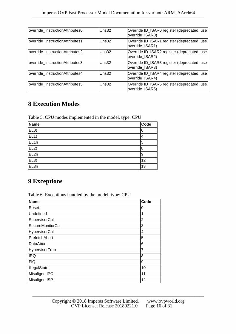
override_InstructionAttributes0 Uns32 Override ID_ISAR0 register (deprecated, useoverride_ISAR0)
override_InstructionAttributes1 Uns32 Override ID_ISAR1 register (deprecated, useoverride_ISAR1)
override_InstructionAttributes2 Uns32 Override ID_ISAR2 register (deprecated, useoverride_ISAR2)
override_InstructionAttributes3 Uns32 Override ID_ISAR3 register (deprecated, useoverride_ISAR3)
override_InstructionAttributes4 Uns32 Override ID_ISAR4 register (deprecated, useoverride_ISAR4)
override_InstructionAttributes5 Uns32 Override ID_ISAR5 register (deprecated, useoverride_ISAR5)
8 Execution Modes
Table 5. CPU modes implemented in the model, type: CPU
Name Code
EL0t 0
EL1t 4
EL1h 5
EL2t 8
EL2h 9
EL3t 12
EL3h 13
9 Exceptions
Table 6. Exceptions handled by the model, type: CPU
Name Code
Reset 0
Undefined 1
SupervisorCall 2
SecureMonitorCall 3
HypervisorCall 4
PrefetchAbort 5
DataAbort 6
HypervisorTrap 7
IRQ 8
FIQ 9
IllegalState 10
MisalignedPC 11
MisalignedSP 12

Imperas OVP Fast Processor Model Documentation for variant: ARM_AArch64————————————————————————————————————
————————————————————————————————————Copyright © 2018 Imperas Software Limited. www.ovpworld.org
OVP License. Release 20180221.0 Page 17 of 31
SError 13

Imperas OVP Fast Processor Model Documentation for variant: ARM_AArch64————————————————————————————————————
————————————————————————————————————Copyright © 2018 Imperas Software Limited. www.ovpworld.org
OVP License. Release 20180221.0 Page 18 of 31
10 Hierarchy of the modelA CPU core may allow the user to configure it to instance many processors of a SymmetricalMulti Processor (SMP). A CPU core may also have sub elements within a processor, forexample hardware threading blocks.OVP processor models can be written to include SMP blocks and to have many levels ofhierarchy.
Some OVP CPU models may have a fixed hierarchy, and some may be configured by settingsin a configuration register. Please see the register definitions of this model.
This model documentation shows the settings and hierarchy of the default settings for thismodel variant.
10.1 Level 1: CPU
This level in the model hierarchy has 5 commands.
This level in the model hierarchy has 6 register groups:
Table 7. Register groups
Group name Registers
Core_AArch64 33
SIMD_FP_AArch64 32
AArch64_system 198
AArch64_system_artifact 1
AArch64_SYS_instruction_registers 55
Integration_support 31
This level in the model hierarchy has no children.

Imperas OVP Fast Processor Model Documentation for variant: ARM_AArch64————————————————————————————————————
————————————————————————————————————Copyright © 2018 Imperas Software Limited. www.ovpworld.org
OVP License. Release 20180221.0 Page 19 of 31
11 Model Commands
11.1 Level 1: CPU
11.1.1 debugflags
show or modify the processor debug flags
Table 8. debugflags command argumentsArgument Type Description
-get Boolean print current processor flags value
-set Int32 new processor flags (only flags 0x000003e4 can be modified)
11.1.2 dumpTLB
report TLB contents
Table 9. dumpTLB command argumentsArgument Type Description
-all Boolean show the contents of all TLBs (if False, show just the currentTLB)
11.1.3 isync
specify instruction address range for synchronous execution
Table 10. isync command argumentsArgument Type Description
-addresshi Uns64 end address of synchronous execution range
-addresslo Uns64 start address of synchronous execution range
11.1.4 itrace
enable or disable instruction tracing
Table 11. itrace command argumentsArgument Type Description
-after Uns64 apply after this many instructions
-enable Boolean enable instruction tracing
-instructioncount Boolean include the instruction number in each trace
-off Boolean disable instruction tracing
-on Boolean enable instruction tracing
-registerchange Boolean show registers changed by this instruction
-registers Boolean show registers after each trace
11.1.5 validateTLB

Imperas OVP Fast Processor Model Documentation for variant: ARM_AArch64————————————————————————————————————
————————————————————————————————————Copyright © 2018 Imperas Software Limited. www.ovpworld.org
OVP License. Release 20180221.0 Page 20 of 31
check TLB contents against page tables in memory and report incoherent entries
Table 12. validateTLB command arguments
Argument Type Description
-all Boolean check all TLBs (if False, validate just the current TLB)
-verbose Boolean show all TLB entries (if False, show only incoherent entries)
12 Registers
12.1 Level 1: CPU
12.1.1 Core_AArch64
Table 13. Registers at level 1, type: CPU, register group: 'Core_AArch64'
Name Bits Initial value (Hex) alias Description
x0 64 0 rw
x1 64 0 rw
x2 64 0 rw
x3 64 0 rw
x4 64 0 rw
x5 64 0 rw
x6 64 0 rw
x7 64 0 rw
x8 64 0 rw
x9 64 0 rw
x10 64 0 rw
x11 64 0 rw
x12 64 0 rw
x13 64 0 rw
x14 64 0 rw
x15 64 0 rw
x16 64 0 rw
x17 64 0 rw
x18 64 0 rw
x19 64 0 rw
x20 64 0 rw
x21 64 0 rw
x22 64 0 rw
x23 64 0 rw
x24 64 0 rw
x25 64 0 rw
x26 64 0 rw
x27 64 0 rw

Imperas OVP Fast Processor Model Documentation for variant: ARM_AArch64————————————————————————————————————
————————————————————————————————————Copyright © 2018 Imperas Software Limited. www.ovpworld.org
OVP License. Release 20180221.0 Page 21 of 31
x28 64 0 rw
x29 64 0 rw frame pointer
x30 64 0 rw
sp 64 0 rw stack pointer
pc 64 0 rw program counter
12.1.2 SIMD_FP_AArch64
Table 14. Registers at level 1, type: CPU, register group: 'SIMD_FP_AArch64'Name Bits Initial value (Hex) alias Description
v0 128 - rw
v1 128 - rw
v2 128 - rw
v3 128 - rw
v4 128 - rw
v5 128 - rw
v6 128 - rw
v7 128 - rw
v8 128 - rw
v9 128 - rw
v10 128 - rw
v11 128 - rw
v12 128 - rw
v13 128 - rw
v14 128 - rw
v15 128 - rw
v16 128 - rw
v17 128 - rw
v18 128 - rw
v19 128 - rw
v20 128 - rw
v21 128 - rw
v22 128 - rw
v23 128 - rw
v24 128 - rw
v25 128 - rw
v26 128 - rw
v27 128 - rw
v28 128 - rw
v29 128 - rw
v30 128 - rw
v31 128 - rw

Imperas OVP Fast Processor Model Documentation for variant: ARM_AArch64————————————————————————————————————
————————————————————————————————————Copyright © 2018 Imperas Software Limited. www.ovpworld.org
OVP License. Release 20180221.0 Page 22 of 31
12.1.3 AArch64_system
Table 15. Registers at level 1, type: CPU, register group: 'AArch64_system'Name Bits Initial value (Hex) alias Description
ACTLR_EL1 64 0 rw Auxiliary Control (EL1)
ACTLR_EL2 64 0 rw Auxiliary Control (EL2)
ACTLR_EL3 64 0 rw Auxiliary Control (EL3)
AFSR0_EL1 32 0 rw Auxiliary Fault Status 0 (EL1)
AFSR0_EL2 32 0 rw Auxiliary Fault Status 0 (EL2)
AFSR0_EL3 32 0 rw Auxiliary Fault Status 0 (EL3)
AFSR1_EL1 32 0 rw Auxiliary Fault Status 1 (EL1)
AFSR1_EL2 32 0 rw Auxiliary Fault Status 1 (EL2)
AFSR1_EL3 32 0 rw Auxiliary Fault Status 1 (EL3)
AIDR_EL1 32 0 r- Auxiliary ID
AMAIR_EL1 64 0 rw Auxiliary Memory AttributeIndirection (EL1)
AMAIR_EL2 64 0 rw Auxiliary Memory AttributeIndirection (EL2)
AMAIR_EL3 64 0 rw Auxiliary Memory AttributeIndirection (EL3)
CCSIDR_EL1 32 701fe00a r- Current Cache Size ID
CLIDR_EL1 32 a000023 r- Cache Level ID
CNTFRQ_EL0 32 4c4b40 rw Counter-Timer Frequency
CNTHCTL_EL2 32 3 rw Counter-Timer HypervisorControl
CNTHP_CTL_EL2 32 0 rw Counter-Timer HypervisorPhysical Timer Control
CNTHP_CVAL_EL2 64 0 rw Counter-Timer HypervisorPhysical Timer CompareValue
CNTHP_TVAL_EL2 32 0 rw Counter-Timer HypervisorPhysical Timer TimerValue
CNTKCTL_EL1 32 0 rw Counter-Timer Kernel Control
CNTPCT_EL0 64 0 r- Counter-Timer Physical Count
CNTPS_CTL_EL1 32 0 rw Counter-Timer PhysicalSecure Timer Control
CNTPS_CVAL_EL1 64 0 rw Counter-Timer PhysicalSecure Timer CompareValue
CNTPS_TVAL_EL1 32 0 rw Counter-Timer PhysicalSecure Timer TimerValue
CNTP_CTL_EL0 32 0 rw Counter-Timer Physical TimerControl
CNTP_CVAL_EL0 64 0 rw Counter-Timer Physical TimerCompareValue
CNTP_TVAL_EL0 32 0 rw Counter-Timer Physical TimerTimerValue

Imperas OVP Fast Processor Model Documentation for variant: ARM_AArch64————————————————————————————————————
————————————————————————————————————Copyright © 2018 Imperas Software Limited. www.ovpworld.org
OVP License. Release 20180221.0 Page 23 of 31
CNTVCT_EL0 64 0 r- Counter-Timer Virtual Count
CNTVOFF_EL2 64 0 rw Counter-Timer Virtual Offset
CNTV_CTL_EL0 32 0 rw Counter-Timer Virtual TimerControl
CNTV_CVAL_EL0 64 0 rw Counter-Timer Virtual TimerCompareValue
CNTV_TVAL_EL0 32 0 rw Counter-Timer Virtual TimerTimerValue
CONTEXTIDR_EL1 32 0 rw Context ID (EL1)
CPACR_EL1 32 0 rw Architectural Feature AccessControl
CPTR_EL2 32 33ff rw Architectural Feature Trap(EL2)
CPTR_EL3 32 0 rw Architectural Feature Trap(EL3)
CSSELR_EL1 32 0 rw Current Size Selection
CTR_EL0 32 8404c004 r- Cache Type
CurrentEL 32 c r- Current Exception Level
DAIF 32 3c0 rw Interrupt Mask Bits
DBGAUTHSTATUS_EL1 32 aa r- Debug Authentication Status
DBGBCR0_EL1 32 0 rw Debug Breakpoint Control 0
DBGBCR1_EL1 32 0 rw Debug Breakpoint Control 1
DBGBCR2_EL1 32 0 rw Debug Breakpoint Control 2
DBGBCR3_EL1 32 0 rw Debug Breakpoint Control 3
DBGBCR4_EL1 32 0 rw Debug Breakpoint Control 4
DBGBCR5_EL1 32 0 rw Debug Breakpoint Control 5
DBGBVR0_EL1 64 0 rw Debug Breakpoint Value 0
DBGBVR1_EL1 64 0 rw Debug Breakpoint Value 1
DBGBVR2_EL1 64 0 rw Debug Breakpoint Value 2
DBGBVR3_EL1 64 0 rw Debug Breakpoint Value 3
DBGBVR4_EL1 64 0 rw Debug Breakpoint Value 4
DBGBVR5_EL1 64 0 rw Debug Breakpoint Value 5
DBGCLAIMCLR_EL1 32 0 rw Debug Claim Tag Clear
DBGCLAIMSET_EL1 32 0 rw Debug Claim Tag Set
DBGDTRTRX_EL0 32 0 rw Debug Data Transfer,Transmit/Receive
DBGDTR_EL0 64 0 rw Debug Data Transfer
DBGPRCR_EL1 32 0 rw Debug Power Control
DBGVCR32_EL2 32 0 rw Debug Vector Catch
DBGWCR0_EL1 32 0 rw Debug Watchpoint Control 0
DBGWCR1_EL1 32 0 rw Debug Watchpoint Control 1
DBGWCR2_EL1 32 0 rw Debug Watchpoint Control 2
DBGWCR3_EL1 32 0 rw Debug Watchpoint Control 3
Imperas OVP Fast Processor Model Documentation for variant: ARM_AArch64————————————————————————————————————
————————————————————————————————————Copyright © 2018 Imperas Software Limited. www.ovpworld.org
OVP License. Release 20180221.0 Page 24 of 31
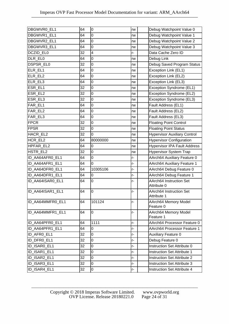
DBGWVR0_EL1 64 0 rw Debug Watchpoint Value 0
DBGWVR1_EL1 64 0 rw Debug Watchpoint Value 1
DBGWVR2_EL1 64 0 rw Debug Watchpoint Value 2
DBGWVR3_EL1 64 0 rw Debug Watchpoint Value 3
DCZID_EL0 32 4 r- Data Cache Zero ID
DLR_EL0 64 0 rw Debug Link
DSPSR_EL0 32 0 rw Debug Saved Program Status
ELR_EL1 64 0 rw Exception Link (EL1)
ELR_EL2 64 0 rw Exception Link (EL2)
ELR_EL3 64 0 rw Exception Link (EL3)
ESR_EL1 32 0 rw Exception Syndrome (EL1)
ESR_EL2 32 0 rw Exception Syndrome (EL2)
ESR_EL3 32 0 rw Exception Syndrome (EL3)
FAR_EL1 64 0 rw Fault Address (EL1)
FAR_EL2 64 0 rw Fault Address (EL2)
FAR_EL3 64 0 rw Fault Address (EL3)
FPCR 32 0 rw Floating Point Control
FPSR 32 0 rw Floating Point Status
HACR_EL2 32 0 rw Hypervisor Auxiliary Control
HCR_EL2 64 80000000 rw Hypervisor Configuration
HPFAR_EL2 64 0 rw Hypervisor IPA Fault Address
HSTR_EL2 32 0 rw Hypervisor System Trap
ID_AA64AFR0_EL1 64 0 r- AArch64 Auxiliary Feature 0
ID_AA64AFR1_EL1 64 0 r- AArch64 Auxiliary Feature 1
ID_AA64DFR0_EL1 64 10305106 r- AArch64 Debug Feature 0
ID_AA64DFR1_EL1 64 0 r- AArch64 Debug Feature 1
ID_AA64ISAR0_EL1 64 0 r- AArch64 Instruction SetAttribute 0
ID_AA64ISAR1_EL1 64 0 r- AArch64 Instruction SetAttribute 1
ID_AA64MMFR0_EL1 64 101124 r- AArch64 Memory ModelFeature 0
ID_AA64MMFR1_EL1 64 0 r- AArch64 Memory ModelFeature 1
ID_AA64PFR0_EL1 64 1111 r- AArch64 Processor Feature 0
ID_AA64PFR1_EL1 64 0 r- AArch64 Processor Feature 1
ID_AFR0_EL1 32 0 r- Auxiliary Feature 0
ID_DFR0_EL1 32 0 r- Debug Feature 0
ID_ISAR0_EL1 32 0 r- Instruction Set Attribute 0
ID_ISAR1_EL1 32 0 r- Instruction Set Attribute 1
ID_ISAR2_EL1 32 0 r- Instruction Set Attribute 2
ID_ISAR3_EL1 32 0 r- Instruction Set Attribute 3
ID_ISAR4_EL1 32 0 r- Instruction Set Attribute 4

Imperas OVP Fast Processor Model Documentation for variant: ARM_AArch64————————————————————————————————————
————————————————————————————————————Copyright © 2018 Imperas Software Limited. www.ovpworld.org
OVP License. Release 20180221.0 Page 25 of 31
ID_ISAR5_EL1 32 0 r- Instruction Set Attribute 5
ID_MMFR0_EL1 32 0 r- Memory Model Feature 0
ID_MMFR1_EL1 32 0 r- Memory Model Feature 1
ID_MMFR2_EL1 32 0 r- Memory Model Feature 2
ID_MMFR3_EL1 32 0 r- Memory Model Feature 3
ID_PFR0_EL1 32 0 r- Processor Feature 0
ID_PFR1_EL1 32 0 r- Processor Feature 1
ISR_EL1 32 0 r- Interrupt Status
MAIR_EL1 64 44e048e000098aa4 rw Memory Attribute Indirection(EL1)
MAIR_EL2 64 0 rw Memory Attribute Indirection(EL2)
MAIR_EL3 64 44e048e000098aa4 rw Memory Attribute Indirection(EL3)
MDCCINT_EL1 32 0 rw Monitor DCC Interrupt Enable
MDCCSR_EL0 32 0 r- Monitor DCC Status
MDCR_EL2 32 6 rw Monitor Debug Configuration(EL2)
MDCR_EL3 32 0 rw Monitor Debug Configuration(EL3)
MDRAR_EL1 64 0 r- Monitor Debug ROM Address
MDSCR_EL1 32 0 rw Monitor Debug SystemControl
MIDR_EL1 32 410fd000 r- Main ID
MPIDR_EL1 64 c0000000 r- Multiprocessor Affinity
MVFR0_EL1 32 0 r- Media and VFP Feature 0
MVFR1_EL1 32 0 r- Media and VFP Feature 1
MVFR2_EL1 32 0 r- Media and VFP Feature 2
NZCV 32 0 rw Condition Flags
OSDLR_EL1 32 0 rw OS Double Lock
OSDTRRX_EL1 32 0 rw OS Lock Data Transfer,Receive
OSDTRTX_EL1 32 0 rw OS Lock Data Transfer,Transmit
OSECCR_EL1 32 0 rw OS Lock Exception CatchControl
OSLAR_EL1 32 - -w OS Lock Access
OSLSR_EL1 32 a r- OS Lock Status
PAR_EL1 64 0 rw Physical Address
PMCCFILTR_EL0 32 0 rw Performance Monitors CycleCount Filter
PMCCNTR_EL0 64 0 rw Performance Monitors CycleCount
PMCEID0_EL0 32 3fff0f3f r- Performance MonitorsCommon Event ID 0

Imperas OVP Fast Processor Model Documentation for variant: ARM_AArch64————————————————————————————————————
————————————————————————————————————Copyright © 2018 Imperas Software Limited. www.ovpworld.org
OVP License. Release 20180221.0 Page 26 of 31
PMCEID1_EL0 32 0 r- Performance MonitorsCommon Event ID 1
PMCNTENCLR_EL0 32 0 rw Performance Monitors CountEnable Clear
PMCNTENSET_EL0 32 0 rw Performance Monitors CountEnable Set
PMCR_EL0 32 410f3000 rw Performance Monitors Control
PMEVCNTR0_EL0 32 0 rw Performance Monitors EventCount 0
PMEVCNTR1_EL0 32 0 rw Performance Monitors EventCount 1
PMEVCNTR2_EL0 32 0 rw Performance Monitors EventCount 2
PMEVCNTR3_EL0 32 0 rw Performance Monitors EventCount 3
PMEVCNTR4_EL0 32 0 rw Performance Monitors EventCount 4
PMEVCNTR5_EL0 32 0 rw Performance Monitors EventCount 5
PMEVTYPER0_EL0 32 0 rw Performance Monitors EventType 0
PMEVTYPER1_EL0 32 0 rw Performance Monitors EventType 1
PMEVTYPER2_EL0 32 0 rw Performance Monitors EventType 2
PMEVTYPER3_EL0 32 0 rw Performance Monitors EventType 3
PMEVTYPER4_EL0 32 0 rw Performance Monitors EventType 4
PMEVTYPER5_EL0 32 0 rw Performance Monitors EventType 5
PMINTENCLR_EL1 32 0 rw Performance MonitorsInterrupt Enable Clear
PMINTENSET_EL1 32 0 rw Performance MonitorsInterrupt Enable Set
PMOVSCLR_EL0 32 0 rw Performance MonitorsOverflow Flag Status Clear
PMOVSSET_EL0 32 0 rw Performance MonitorsOverflow Flag Status Set
PMSELR_EL0 32 0 rw Performance Monitors EventCounter Selection
PMSWINC_EL0 32 - -w Performance MonitorsSoftware Increment
PMUSERENR_EL0 32 0 rw Performance Monitors UserEnable
PMXEVCNTR_EL0 32 0 rw Performance MonitorsSelected Event Count
Imperas OVP Fast Processor Model Documentation for variant: ARM_AArch64————————————————————————————————————
————————————————————————————————————Copyright © 2018 Imperas Software Limited. www.ovpworld.org
OVP License. Release 20180221.0 Page 27 of 31
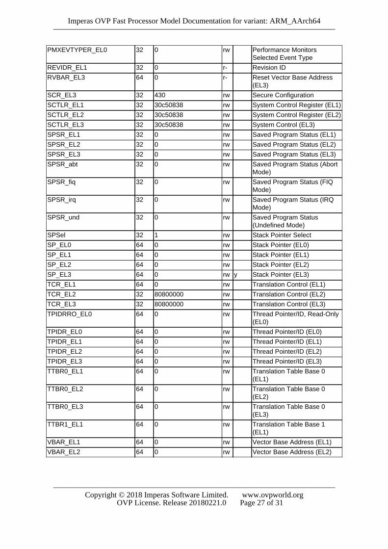
PMXEVTYPER_EL0 32 0 rw Performance MonitorsSelected Event Type
REVIDR_EL1 32 0 r- Revision ID
RVBAR_EL3 64 0 r- Reset Vector Base Address(EL3)
SCR_EL3 32 430 rw Secure Configuration
SCTLR_EL1 32 30c50838 rw System Control Register (EL1)
SCTLR_EL2 32 30c50838 rw System Control Register (EL2)
SCTLR_EL3 32 30c50838 rw System Control (EL3)
SPSR_EL1 32 0 rw Saved Program Status (EL1)
SPSR_EL2 32 0 rw Saved Program Status (EL2)
SPSR_EL3 32 0 rw Saved Program Status (EL3)
SPSR_abt 32 0 rw Saved Program Status (AbortMode)
SPSR_fiq 32 0 rw Saved Program Status (FIQMode)
SPSR_irq 32 0 rw Saved Program Status (IRQMode)
SPSR_und 32 0 rw Saved Program Status(Undefined Mode)
SPSel 32 1 rw Stack Pointer Select
SP_EL0 64 0 rw Stack Pointer (EL0)
SP_EL1 64 0 rw Stack Pointer (EL1)
SP_EL2 64 0 rw Stack Pointer (EL2)
SP_EL3 64 0 rw y Stack Pointer (EL3)
TCR_EL1 64 0 rw Translation Control (EL1)
TCR_EL2 32 80800000 rw Translation Control (EL2)
TCR_EL3 32 80800000 rw Translation Control (EL3)
TPIDRRO_EL0 64 0 rw Thread Pointer/ID, Read-Only(EL0)
TPIDR_EL0 64 0 rw Thread Pointer/ID (EL0)
TPIDR_EL1 64 0 rw Thread Pointer/ID (EL1)
TPIDR_EL2 64 0 rw Thread Pointer/ID (EL2)
TPIDR_EL3 64 0 rw Thread Pointer/ID (EL3)
TTBR0_EL1 64 0 rw Translation Table Base 0(EL1)
TTBR0_EL2 64 0 rw Translation Table Base 0(EL2)
TTBR0_EL3 64 0 rw Translation Table Base 0(EL3)
TTBR1_EL1 64 0 rw Translation Table Base 1(EL1)
VBAR_EL1 64 0 rw Vector Base Address (EL1)
VBAR_EL2 64 0 rw Vector Base Address (EL2)
Imperas OVP Fast Processor Model Documentation for variant: ARM_AArch64————————————————————————————————————
————————————————————————————————————Copyright © 2018 Imperas Software Limited. www.ovpworld.org
OVP License. Release 20180221.0 Page 28 of 31
VBAR_EL3 64 0 rw Vector Base Address (EL3)
VMPIDR_EL2 64 c0000000 rw Virtualization MultiprocessorID
VPIDR_EL2 32 410fd000 rw Virtualization Processor ID
VTCR_EL2 32 80000000 rw Virtualization TranslationControl
VTTBR_EL2 64 0 rw Virtualization TranslationTable Base
12.1.4 AArch64_system_artifact
Table 16. Registers at level 1, type: CPU, register group: 'AArch64_system_artifact'Name Bits Initial
value (Hex)alias Description
cpsr 32 3cd rw
12.1.5 AArch64_SYS_instruction_registers
Table 17. Registers at level 1, type: CPU, register group:'AArch64_SYS_instruction_registers'Name Bits Initial value (Hex) alias Description
ALLE1 64 - -w
ALLE1IS 64 - -w
ALLE2 64 - -w
ALLE2IS 64 - -w
ALLE3 64 - -w
ALLE3IS 64 - -w
ASIDE1 64 - -w
ASIDE1IS 64 - -w
CISW 32 - -w
CIVAC 64 - -w
CSW 32 - -w
CVAC 64 - -w
CVAU 64 - -w
IALLU 32 - -w
IALLUIS 32 - -w
IPAS2E1 64 - -w
IPAS2E1IS 64 - -w
IPAS2LE1 64 - -w
IPAS2LE1IS 64 - -w
ISW 32 - -w
IVAC 64 - -w
IVAU 64 - -w
S1E0R 64 - -w
S1E0W 64 - -w

Imperas OVP Fast Processor Model Documentation for variant: ARM_AArch64————————————————————————————————————
————————————————————————————————————Copyright © 2018 Imperas Software Limited. www.ovpworld.org
OVP License. Release 20180221.0 Page 29 of 31
S1E1R 64 - -w
S1E1W 64 - -w
S1E2R 64 - -w
S1E2W 64 - -w
S1E3R 64 - -w
S1E3W 64 - -w
S12E0R 64 - -w
S12E0W 64 - -w
S12E1R 64 - -w
S12E1W 64 - -w
VAAE1 64 - -w
VAAE1IS 64 - -w
VAALE1 64 - -w
VAALE1IS 64 - -w
VAE1 64 - -w
VAE1IS 64 - -w
VAE2 64 - -w
VAE2IS 64 - -w
VAE3 64 - -w
VAE3IS 64 - -w
VALE1 64 - -w
VALE1IS 64 - -w
VALE2 64 - -w
VALE2IS 64 - -w
VALE3 64 - -w
VALE3IS 64 - -w
VMALLE1 64 - -w
VMALLE1IS 64 - -w
VMALLS12E1 64 - -w
VMALLS12E1IS 64 - -w
ZVA 32 - -w
12.1.6 Integration_support
Table 18. Registers at level 1, type: CPU, register group: 'Integration_support'Name Bits Initial value (Hex) alias Description
transactPL 32 3 r- privilege level of current memorytransaction
transactAT 32 0 r- current memory transaction type:PA=1, VA=0
artifactPAR 64 0 r- result of address translation for artifactwrite to ATS1CPR etc
PTWBankSelect 8 0 rw select PTW bank (0 is stage 1, 1 isstage 2, 2-5 are stage 2 walks initiated
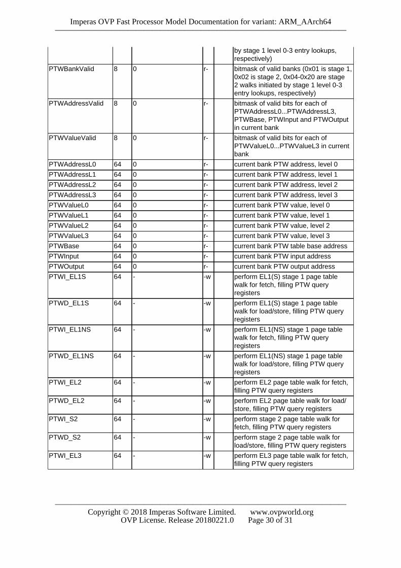
Imperas OVP Fast Processor Model Documentation for variant: ARM_AArch64————————————————————————————————————
————————————————————————————————————Copyright © 2018 Imperas Software Limited. www.ovpworld.org
OVP License. Release 20180221.0 Page 30 of 31
by stage 1 level 0-3 entry lookups,respectively)
PTWBankValid 8 0 r- bitmask of valid banks (0x01 is stage 1,0x02 is stage 2, 0x04-0x20 are stage2 walks initiated by stage 1 level 0-3entry lookups, respectively)
PTWAddressValid 8 0 r- bitmask of valid bits for each ofPTWAddressL0...PTWAddressL3,PTWBase, PTWInput and PTWOutputin current bank
PTWValueValid 8 0 r- bitmask of valid bits for each ofPTWValueL0...PTWValueL3 in currentbank
PTWAddressL0 64 0 r- current bank PTW address, level 0
PTWAddressL1 64 0 r- current bank PTW address, level 1
PTWAddressL2 64 0 r- current bank PTW address, level 2
PTWAddressL3 64 0 r- current bank PTW address, level 3
PTWValueL0 64 0 r- current bank PTW value, level 0
PTWValueL1 64 0 r- current bank PTW value, level 1
PTWValueL2 64 0 r- current bank PTW value, level 2
PTWValueL3 64 0 r- current bank PTW value, level 3
PTWBase 64 0 r- current bank PTW table base address
PTWInput 64 0 r- current bank PTW input address
PTWOutput 64 0 r- current bank PTW output address
PTWI_EL1S 64 - -w perform EL1(S) stage 1 page tablewalk for fetch, filling PTW queryregisters
PTWD_EL1S 64 - -w perform EL1(S) stage 1 page tablewalk for load/store, filling PTW queryregisters
PTWI_EL1NS 64 - -w perform EL1(NS) stage 1 page tablewalk for fetch, filling PTW queryregisters
PTWD_EL1NS 64 - -w perform EL1(NS) stage 1 page tablewalk for load/store, filling PTW queryregisters
PTWI_EL2 64 - -w perform EL2 page table walk for fetch,filling PTW query registers
PTWD_EL2 64 - -w perform EL2 page table walk for load/store, filling PTW query registers
PTWI_S2 64 - -w perform stage 2 page table walk forfetch, filling PTW query registers
PTWD_S2 64 - -w perform stage 2 page table walk forload/store, filling PTW query registers
PTWI_EL3 64 - -w perform EL3 page table walk for fetch,filling PTW query registers

Imperas OVP Fast Processor Model Documentation for variant: ARM_AArch64————————————————————————————————————
————————————————————————————————————Copyright © 2018 Imperas Software Limited. www.ovpworld.org
OVP License. Release 20180221.0 Page 31 of 31
PTWD_EL3 64 - -w perform EL3 page table walk for load/store, filling PTW query registers
PTWI_current 64 - -w perform current mode page table walkfor fetch, filling PTW query registers
PTWD_current 64 - -w perform current mode page tablewalk for load/store, filling PTW queryregisters
HaltReason 8 0 r- bit field indicating halt reason
#


![Index [] · 2015-01-08 · mcz ovp cl 48vuc 1,25a 8449040000 b.115 mcz ovp cl fg 24vuc 0,5a 8704240000 b.118 mcz ovp filter 24v 0,5a 8449100000 b.119 mcz ovp gasableiter 90v 8449130000](https://static.fdocuments.in/doc/165x107/5e96e66af12683124d138cf4/index-2015-01-08-mcz-ovp-cl-48vuc-125a-8449040000-b115-mcz-ovp-cl-fg-24vuc.jpg)


