Semiconductor Device Modeling and Characterization EE5342, Lecture 20 -Sp 2002

1
Semiconductor device modeling
with SCAPS-1D
Lecture 4
Special Topics:
Device Modeling
Outline
• Basic concepts and physics model
• Overview of capabilities
• Input/Output
• Brief literature survey of problems/results
• Hands on: running standard models,
creating a simple model
SCAPS-1D
• SCAPS (a Solar Cell Capacitance Simulator) is a
one-dimensional solar cell simulation program
• Developed at the Department of Electronics and
Information Systems (ELIS) of the University of
Gent, Belgium
• The program is freely available to the research
community (reference it in your publications)
• Continuously supported and further developed
(http://scaps.elis.ugent.be); runs under Windows
SCAPS-1D
• Originally developed for polycrystalline cell structures
of the CuInSe2 and the CdTe family
– Basis reference paper published in 2000
• Designed to accommodate thin films, multiple
interfaces, large band gaps (Eg=1.12eV for Si, but
2.4eV for CdS used as window layer)
• The package evolved over the years to include
additional mechanisms, e.g., Auger recombination,
tunneling, multiple enhancement to user interface, etc.
Device model
• Device is modeled in one
dimension across layers,
and formed junctions in
physical space
• Depth is x coordinate
• Spatial distributions of
fields, charge carriers,
defects, etc.
Metal/TCO
metal
n-doped semiconductor
p-doped semiconductor
1-D direction,
x coordinate
Device model: energy space
• Band diagram of a realistic
p-n heterojunction with back
barrier and defect states at
thermodynamic equilibrium
• Compared to AMPS: better
description of recombination
processes; several tunneling
mechanisms are included in
SCAPS
EF
V1
V2
Defect states
semiconductors metal
n-type
p-type

2
Physics model: governing
equations
• The Poisson equation, and the continuity equations
for electrons and holes (same as in AMPS-1D)
),(
1)(
0
pnq
NNpnq
xx
xdefDA
t
ppnUG
x
j
t
npnUG
x
j
p
p
n
n
),(
),(p,n – free carrier concentrationsN±
D,A – charged dopantsdef(n,p) – defect distributions
jn, jp – the electron and hole current densitiesUn,p - the net recombination rates;
G - the generation rate
Physics model: solving
governing equations • Constitutive relations
• Solve for potential and quasi-Fermi levels
• Boundary conditions at interfaces and contacts
• Structure is discretized, meshing refined around interfaces
• Newton-Raphson method with algorithm modifications
x
E
qj
x
E
qj
Fpp
p
Fnn
n
;
Physics model: interfaces
• The quasi-fermi levels are allowed to be
discontinuous at the interfaces
• Recombination at the interface states is handled
Example: recombination
between electrons of CdS
and holes in the CdTe on the
right side of the interface
Physics model: grading
• Almost all parameters can be graded; the principles
of the algorithms used to simulate graded solar cell
structures
• All parameters are consistently derived from the
composition grading of a layer
– Each layer is assumed to have composition A1-yBy
– Define values of a parameter P for pure compounds A, B,
and the composition grading y(x) over the layer thickness
– Specify some grading law for P(y)
Physics model: grading
• Grading laws:
uniform, linear,
exponential, etc.
• Alternatively,
the composition
grading profile
can be loaded
from a file
Physics model: generation
• From internal calculation under illumination
– Dark or light, power level (~ND filter), choice of the
illuminated side, choice of the spectrum
• From user supplied generation g(x) file, at the x-
coordinates of the nodes used by SCAPS
– allows for modeling of radiation detectors, EBIC
measurements
– Solar cell efficiency and QE cannot be calculated; may
use collection efficiency, based on “ ideal” device current
3
Physics model: recombination
• Direct band-to-band
– Between the occupied states in the CB and the vacant
states in the VB
• Indirect, or Shockley-Read-Hall
– Through a defect state in the gap
– Also through interface states
• Auger recombination
– Involves three carriers: after recombination, the energy is
given an electron in the conduction band (as opposed to
emission as a photon or phonon)
Physics model: tunneling
• The following tunneling mechanisms are treated: band to
band tunneling, intraband tunneling, tunneling to interface
defects and tunneling to contacts
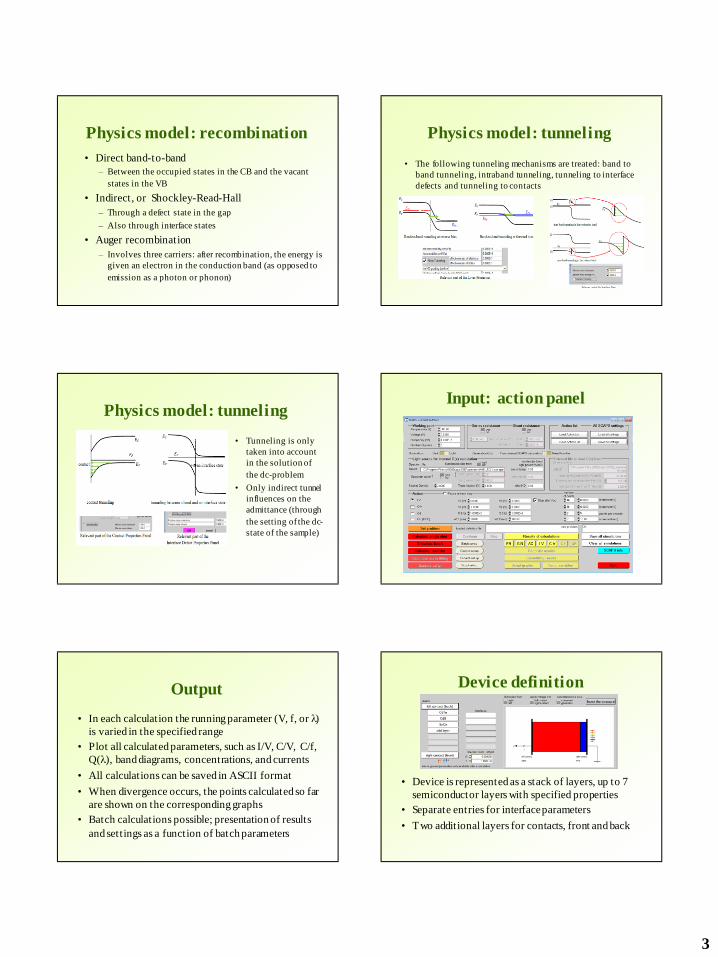
Physics model: tunneling
• Tunneling is only
taken into account
in the solution of
the dc-problem
• Only indirect tunnel
influences on the
admittance (through
the setting of the dc-
state of the sample)
Input: action panel
Output
• In each calculation the running parameter (V, f, or l)
is varied in the specified range
• Plot all calculated parameters, such as I/V, C/V, C/f,
Q(l), band diagrams, concentrations, and currents
• All calculations can be saved in ASCII format
• When divergence occurs, the points calculated so far
are shown on the corresponding graphs
• Batch calculations possible; presentation of results
and settings as a function of batch parameters
Device definition
• Device is represented as a stack of layers, up to 7
semiconductor layers with specified properties
• Separate entries for interface parameters
• Two additional layers for contacts, front and back

4
Quantum efficiency
• The Q.E. is the ratio of the number of carriers
collected by the solar cell to the number of photons
of a given energy incident on the solar cell
• If all photons of a certain wavelength are absorbed
and the resulting minority carriers are collected,
then the quantum efficiency at that particular
wavelength is unity
• The quantum efficiency for photons with energy
below the band gap is zero
Quantum efficiency
Image from ASU PV education website
http://www.pveducation.org/pvcdrom/solar-cell-operation/quantum-efficiency
Admittance spectroscopy
• Small signal analysis, C(V) of C(f)
• The cell structure is analyzed as if it were a
parallel connection of a (frequency dependent)
capacitance and a (frequency dependent)
conductance
)()(~
~
)( GCiu
JY
ext
T. Walter, R. Herberholz, C. Müller, H.W. Schock, Determination of defect distributions from admittance measurements and application to Cu(In,Ga)Se2 based heterojunctions, Journal of Applied Physics, 80 (1996) 4411-4420.
K. Decock, S. Khelifi, S. Buecheler, F. Pianezzi, A.N. Tiwari, M. Burgelman, Defect distributions in thin film solar cells deduced from admittance measurements under different bias voltages, Journal of Applied Physics, 110 (2011) 063722
Admittance spectroscopy
• The C–V profiling tests the spatial charge distribution (1/C2 vs V gives total defect + dopants concentration)
• Frequency dependent admittance Y() is generally attributed to defects
• In response to the small testing ac electric potential, defects change their occupation numbers
depending on their relaxation times
• Changing (and E=kTln(t0)) – scan energies of resonant states
• Changing bias and bend bending – scan along distance from CB
Contribute to admittance
Output
From standard I-V curves at different levels of illumination
Output
To temperature-dependent admittance spectroscopy (C/f)
Fewer levels at Ew

5
Data analysis features
• Data analysis is supported within the package: any
ASCII-text file can be read as a measurement file
– The file extension indicates which kind of measurement
it contains: ‘ .iv’, ‘ .cv’, ‘ .cf’ or ‘ .qe’
• A built-in curve fitt ing facility
• Quantum efficiency panel
• A panel for the interpretation of admittance
measurements (C/f and C/V)
BRIEF LITERATURE SURVEY
OF PROBLEMS AND RESULTS
SCAPS-1D
Analysis of graded band gap solar cells with SCAPSM. Burgelman and J. Marleinthin, 23rd European PV
Conference, Valencia, Spain, 2008
• In Cu(In,Ga)(Se,S)2
devices the absorber
materials are
engineered to have an
optimized band gap
energy Eg (trade-off
between high current
for low Eg and high
voltage for high Eg)
Analysis of graded band gap solar
cells with SCAPS
Ga- content should be low over most of the CIGS bulk, but high in a narrow region at the back contact and at the interface; a characteristic width < 50 nm seems to be sufficient to combine high Jsc with high Voc
Advanced electrical simulation of thin film solar cellsM. Burgelman, K. Decock, S. Khelif i and A. Abass, Thin Solid
Films, 535 (2013) 296-301
• The result of measurements performed on CIGS
based solar cells depends on history of the sample
• The model includes band gap grading, multivalent
defects and metastable transitions between defects
– The occupation of metastable defects is set during initial
conditions at higher temperature, and then frozen in during
cell operation at lower temperature
– Metastable states of the double vacancy type (VSe–VCu)
were introduced
Advanced electrical simulation of thin film solar cells
A band gap grading profile was set that results in a small but
influential hump or energy barrier in the conduction band
EC
EV

6
Advanced electrical simulation of thin film solar cells
• A barrier in the CB impedes the collection of electrons that are
generated in the absorber to the left of the barrier
• Results in light current reduction at FB thus affecting FF
Modeling metastabilities in chalcopyrite-based thin f ilm solar cells
K. Decock, P. Zabierowski, and M. Burgelman, J. Appl. Phys.
111, 043703 (2012)
• The effect of voltage induced metastabilities on
the capacitance-voltage characteristics of CIGS
• Defect, (VSe-VCu) complex, transitioning from
charged donor to charged acceptor configuration
• The agreement between the simulation and
measurement results has been obtained using a
simple model, and optimizing only 5 parameters
– ETR, the shallow doping density NA, the (VSe-VCu)
complex density NM, the density N t of the additional
acceptor defect and its energy E t.
Modeling metastabilities in
chalcopyrite-based thin film solar cellsSy mbols represent measurement results
Design and optimization of large area thin-film CdTe
detector for radiation therapy imaging applicationsE. I. Parsai, D. Shvydka, J. Kang, Med. Phys. 37 (2010) 3980
• Investigate performance of thin-film CdTe
material in detecting 6MV x-rays
• The utilization of this material has become technologically
feasible only in recent years due to significant development
in large area photovoltaic applications
• Extensive MCNP simulations to evaluate geometrical
parameters, detective quantum efficiency, scatter
• Results of absorbed energy simulation were used in device
operation modeling (with SCAPS) to predict the detector
output signal, and compared with measured signal
Design and optimization of large area
thin-film CdTe
0 20 40 60 80 100
3x10¹⁴
4x10¹⁴
5x10¹⁴
6x10¹⁴
CdTe thickness
10 m
30 m
100 m
e-h
pa
irs,
cm
-3s
-1
Depth, m
0.0 0.1 0.2 0.3
-25
0
25
50
75
Curr
ent density, nA
/cm
2
Voltage, V
CdTe thickness
10 m
30 m
100 m
• MC modeled electron-hole generation profiles were used as input for SCAPS
• CdTe/CdS solar cell with a built-in junction field of ~104 V/cm; the resulting readout voltages are >100 mV for detector layers working in PV mode
Design and optimization of large area
thin-film CdTe
• Better quality of material results in higher readout signals
• Defect density study was only possible for the standard solar cell device thickness range (4-10m)

7
Modeling the ef fect of 1 MeV electron irradiation on the
performance of n+–p–p+ silicon space solar cells A. Hamache, N. Sengouga, A. Meftah, M. Henini, Radiation Physics
and Chemistry 123 (2016) 103–108
• Performance of cells used
in space degrades after
irradiation; anomalous
increase in performance
right before failure
• Analyzed several defects
(experimentally
established) which act as
recombination centers
and/or traps of free
carriers
~50m
Modeling the effect of 1 MeV
electron irradiation
It was concluded that a shallower donor trap is responsible for the phenomenon while the deeper donor trap enhances this phenomenon
Summary
• SCAPS-1D is a versatile package for
semiconductor device modeling
• Output for I/V, C/V, C/f, Q(l), band diagrams,
concentrations, and currents
• Data analysis for I-V, C-V, C-f
• A number of standard models available with the
distribution package
• Well-developed user interface, convenient
scripting facilities
References
• SCAPS manual, M. Burgelman, K. Decock, A. Niemegeers,
J. Verschraegen, S. Degrave, Version: 17 february 2016
• SCAPS 3.0, An introduction, K. Decock and M. Burgelman
• M. Burgelman, P . Nollet, S. Degrave, Thin Solid Films 361
(2000) 527
• Additional references are provided within slides