Oscillator DesignGuide - Keysightliterature.cdn.keysight.com/litweb/pdf/ads2005a/pdf/dgosc.pdf ·...
62
Oscillator DesignGuide August 2005
Transcript of Oscillator DesignGuide - Keysightliterature.cdn.keysight.com/litweb/pdf/ads2005a/pdf/dgosc.pdf ·...

Oscillator DesignGuide
August 2005

Notice
The information contained in this document is subject to change without notice.
Agilent Technologies makes no warranty of any kind with regard to this material,including, but not limited to, the implied warranties of merchantability and fitnessfor a particular purpose. Agilent Technologies shall not be liable for errors containedherein or for incidental or consequential damages in connection with the furnishing,performance, or use of this material.
Warranty
A copy of the specific warranty terms that apply to this software product is availableupon request from your Agilent Technologies representative.
Restricted Rights Legend
Use, duplication or disclosure by the U. S. Government is subject to restrictions as setforth in subparagraph (c) (1) (ii) of the Rights in Technical Data and ComputerSoftware clause at DFARS 252.227-7013 for DoD agencies, and subparagraphs (c) (1)and (c) (2) of the Commercial Computer Software Restricted Rights clause at FAR52.227-19 for other agencies.
© Agilent Technologies, Inc. 1983-2005395 Page Mill Road, Palo Alto, CA 94304 U.S.A.
Acknowledgments
Mentor Graphics is a trademark of Mentor Graphics Corporation in the U.S. andother countries.
Microsoft®, Windows®, MS Windows®, Windows NT®, and MS-DOS® are U.S.registered trademarks of Microsoft Corporation.
Pentium® is a U.S. registered trademark of Intel Corporation.
PostScript® and Acrobat® are trademarks of Adobe Systems Incorporated.
UNIX® is a registered trademark of the Open Group.
Java™ is a U.S. trademark of Sun Microsystems, Inc.
SystemC® is a registered trademark of Open SystemC Initiative, Inc. in the UnitedStates and other countries and is used with permission.
ii

Contents1 Oscillator QuickStart Guide
Using DesignGuides................................................................................................. 1-1Accessing the Documentation............................................................................ 1-3
Basic Procedures ..................................................................................................... 1-4Component Sub-menu Structure........................................................................ 1-5Oscillator Sub-menu Structure ........................................................................... 1-5Design Flow Example......................................................................................... 1-9Oscillator Performance ....................................................................................... 1-11
2 Oscillator DesignGuide ReferenceOscillator Design Guide Structure ............................................................................ 2-1
Push-Button Nonlinear Measurements .............................................................. 2-2Descriptions of Push-Button Measurements ...................................................... 2-2Linear and Nonlinear Design Tools..................................................................... 2-4Descriptions of Design Tools .............................................................................. 2-4Components and Component Characterization Tools ........................................ 2-6Available Components........................................................................................ 2-6Oscillator Core Circuits....................................................................................... 2-8Available Component Characterization Tools ..................................................... 2-16
Generic Oscillator Example ...................................................................................... 2-18Oscillator Simulation........................................................................................... 2-19Linear Design Tools ............................................................................................ 2-25
Solving Harmonic Balance Convergence Problems................................................. 2-35Oscillator Core Examples ......................................................................................... 2-36
Oscillator Core Series Resonator Connection Alternatives................................ 2-38Additional Examples........................................................................................... 2-40Crystal Oscillator (XTO)...................................................................................... 2-40SAW Resonator Oscillator (SAW) ...................................................................... 2-40Voltage Controlled Oscillator (VCO) ................................................................... 2-40YIG Tuned Oscillator (YTO)................................................................................ 2-41
Bibliography .............................................................................................................. 2-42Selected Papers ................................................................................................. 2-43
Index
iii

iv

Chapter 1: Oscillator QuickStart GuideThe Oscillator QuickStart Guide serves as a simple introduction to using theOscillator DesignGuide. For more detailed reference information, refer to Chapter 2,Oscillator DesignGuide Reference.
The DesignGuide is applicable to any oscillator, but is especially useful for RF Boardand Microwave applications. It is designed to help both experts and novices to createdesigns of various complexity.
Note This manual is written describing and showing access through the cascadingmenu preference. If you are running the program through the selection dialog boxmethod, the appearance and interface will be slightly different.
Using DesignGuidesAll DesignGuides can be accessed in the Schematic window through either cascadingmenus or dialog boxes. You can configure your preferred method in the AdvancedDesign System Main window. Select the DesignGuide menu.
The commands in this menu are as follows:
DesignGuide Studio Documentation > Developer Studio Documentation is only availableon this menu if you have installed the DesignGuide Developer Studio. It brings upthe DesignGuide Developer Studio documentation. Another way to access theDeveloper Studio documentation is by selecting Help > Topics and Index >DesignGuides > DesignGuide Developer Studio (from any ADS program window).
DesignGuide Developer Studio > Start DesignGuide Studio is only available on thismenu if you have installed the DesignGuide Developer Studio. It launches the initialDeveloper Studio dialog box.
Add DesignGuide brings up a directory browser in which you can add a DesignGuideto your installation. This is primarily intended for use with DesignGuides that arecustom-built through the Developer Studio.
List/Remove DesignGuide brings up a list of your installed DesignGuides. Select anythat you would like to uninstall and choose the Remove button.
Using DesignGuides 1-1
Oscillator QuickStart Guide
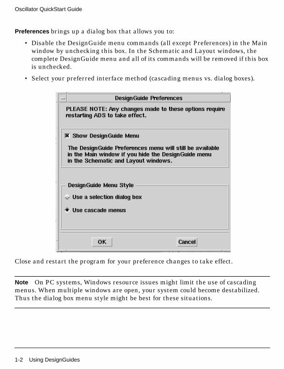
Preferences brings up a dialog box that allows you to:
• Disable the DesignGuide menu commands (all except Preferences) in the Mainwindow by unchecking this box. In the Schematic and Layout windows, thecomplete DesignGuide menu and all of its commands will be removed if this boxis unchecked.
• Select your preferred interface method (cascading menus vs. dialog boxes).
Close and restart the program for your preference changes to take effect.
Note On PC systems, Windows resource issues might limit the use of cascadingmenus. When multiple windows are open, your system could become destabilized.Thus the dialog box menu style might be best for these situations.
1-2 Using DesignGuides

Accessing the Documentation
To access the documentation for the DesignGuide, select either of the following:
• DesignGuide > Oscillator > Oscillator DesignGuide Documentation (from ADSSchematic window)
• Help > Topics and Index > DesignGuides > Oscillator (from any ADS programwindow)
Using DesignGuides 1-3

Oscillator QuickStart Guide
Basic ProceduresAccess the Oscillator DesignGuide from the ADS Schematic window. Select DesignGuide > Oscillator Design Guide, as shown here. All features of the Design Guide areavailable from the Oscillator DesignGuide menu.
The Guide contains the following:
• Nine oscillator circuits (Generic Oscillator, Clapp Oscillator, Hartley Oscillator,Modified Clapp Oscillator, Modified Colpitts Oscillator, XTO, SAW, VCO, andYTO), containing ready-to-use typical oscillator structures for fixed frequency(XTO, SAW) and tunable (VCO, YTO) oscillators in various frequency ranges.
• Component library (Components), providing useful building blocks for oscillatordesign.
• Selection of circuits that simulate their behavior (ComponentCharacterization), providing simulations that characterize 1-ports and 2-ports.
1-4 Basic Procedures
Note Selection of a component brings a component into a design. All other selections(oscillators and component characterization) bring a circuit and simulation into adesign (replacing a previous design).
Component Sub-menu Structure
The Components menu contains a small custom library of resonators and devices,which can help in either modifying an existing oscillator or assembling a new one.They include: device DC and S-parameter characteristics and resonator and filterS-parameter and impedance/admittance characteristics
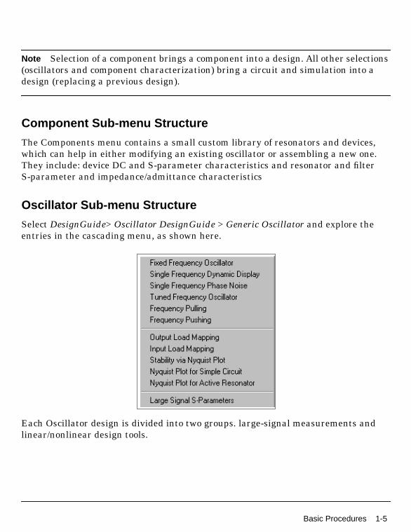
Oscillator Sub-menu Structure
Select DesignGuide> Oscillator DesignGuide > Generic Oscillator and explore theentries in the cascading menu, as shown here.
Each Oscillator design is divided into two groups. large-signal measurements andlinear/nonlinear design tools.
Basic Procedures 1-5

Oscillator QuickStart Guide
Easy-to-use large-signal measurements (for push-button nonlinear analysis), containsimulations of the following:
• Single-frequency oscillations
• Phase noise
• Tuned oscillations
• Frequency pulling
• Frequency pushing
This group is recommended as starting point for both an expert and a novice user. Forthe expert, it provides an overview of tool capabilities. For the novice user, it providesa working oscillator together with simulations of its typical characteristics. You canchoose either the Generic Oscillator, Clapp Oscillator, Hartley Oscillator, ModifiedClapp Oscillator, Modified Colpitts Oscillator, or one of the examples (XTO, SAW,VCO, YTO) to start a desired application.
Linear and nonlinear design tools include Output Load Mapping, Input Load Mapping,Stability via Nyquist Plot, Nyquist Plot for Simple Circuit, Nyquist Plot for ActiveResonator, and Large Signal S-Parameters.
These tools are intended as an aide in designing an oscillator from scratch and ingaining insight into an existing oscillator. The full choice of tools is contained in theGeneric Oscillator. The examples use only those tools that are useful in theirparticular case. The full set of tools include the following:
• Load mapping for load-to-resonator
• Resonator-to-load
• Nyquist stability criterion for varying Zo
• Two additional examples (only in Generic Oscillator), explaining the role of Zo
For nonlinear designs, large-signal S-parameters are defined and applied to oscillatorpower and frequency prediction.
1-6 Basic Procedures

Tools Sub-menu Structure
These utilities provide added functionality to this DesignGuide. A brief description isprovided for each. For more information select the help button located in each utility.
Transistor Bias Utility
The Transistor Bias Utility provides SmartComponents and automated-assistants forthe design and simulation of common resistive and active transistor bias networks.The automated capabilities can determine the transistor DC parameters, design anappropriate network to achieve a given bias point, and simulate and display theachieved performance. All SmartComponents can be modified when selected. Yousimply select a SmartComponent and with little effort redesign or verify theirperformance.
Basic Procedures 1-7

Oscillator QuickStart Guide
Smith Chart Utility
This DesignGuide Utility provides full smith chart capabilities, synthesis of matchingnetworks, allowing impedance matching and plotting of constantGain/Q/VSWR/Noise circles. This guide assumes you have installed the associatedDesignGuide with appropriate licensing codewords.
Impedance Matching Utility
The Impedance Matching Utility performs the synthesis of lumped and distributedimpedance matching networks based on provided specifications. The Utility featuresautomatic simulation, sensitivity analysis, and display setup to enable simple andefficient component verification.
1-8 Basic Procedures

Design Flow Example
Following is a simple design flow example for a fixed frequency oscillator.
Preliminary Steps
1. Open ADS.
2. Open a new or existing project.
3. Open a new Schematic window.
4. Select DesignGuide > Oscillator DesignGuide .
5. Select Crystal Oscillator (XTO) > Stability via Nyquist Plot .
Basic Procedures 1-9

Oscillator QuickStart Guide
Important Preliminary Decisions
The schematic hides the following important choices:
• Device (a BJT)
• Biasing circuit
• Feedback scheme (Colpitts used in OsCore)
• Biasing point, which is shown in the OsCore subcircuit (which you can see fromthe Schematic window by clicking the OsCore component in the design, thenpressing the down-arrow from the Main menu). The schematic is shown in thefollowing illustration.
1-10 Basic Procedures

Moreover, the 30 MHz resonance frequency is assumed and the 20-ohm loadresistance that models the actual load seen through a buffer amplifier and amatching circuit. At this point, you might want to modify the resonator and theOsCore (or replace them by your own circuit).
The modified circuit can be saved as a new design. We want the S11 trace shown onthe polar plot in the data display window to encircle the point 1+j*0. If this does nothappen, the circuit must be modified. In that case, the menu selections Output LoadMapping and Input Load Mapping will help in determining the circuit and the loadmatching. Refer to the Chapter 2, Oscillator DesignGuide Reference for details.
Oscillator Performance
The following menu selections determine the oscillator performance:
• Fixed Frequency Oscillator
• Single Frequency Phase Noise
• Frequency Pulling
• Frequency Pushing
They determine the oscillation frequency and power, phase and amplitude noise, andcircuit elements that contribute most to noise.
You can find frequency variations with load and bias. Modify (or replace) thesubcircuits (the resonator, the OsCore, and the load resistance).
Basic Procedures 1-11
Oscillator QuickStart Guide
1-12 Basic Procedures

Chapter 2: Oscillator DesignGuideReferenceThis manuals provides reference information on the use of the OscillatorDesignGuide.
Oscillator Design Guide StructureThe Oscillator DesignGuide is integrated into Agilent EEsof ’s Advanced DesignSystem environment, working as a smart library and interactive handbook for thecreation of useful designs. It allows you to quickly design oscillators, interactivelycharacterize their components, and receive in-depth insight into their operation. It iseasily modifiable to user-defined configurations. The first release of this DesignGuidefocuses on RF printed circuit boards and microwave oscillations.
In addition to the requirements of the ADS software, the Oscillator DesignGuiderequires approximately 30 MBytes of additional storage space.
Note This manual assumes that you are familiar with all of the basic ADS programoperations. For additional information, refer to the Schematic Capture and Layoutmanual.
The Oscillator DesignGuide contains templates that can be used in the ADS softwareenvironment. It consists of generic colpitts, clapp, modified colpitts, modified clapp,and hartley oscillator design examples, and a library of components and componentcharacterization tools.
To assist both expert and novice oscillator developers in creating designs of variouscomplexity, each example design is divided into three groups:
• Quick and simple push-button nonlinear oscillator measurements
• Easy-to-use design tools for small- and large-signal designs
• Customized library of components and component characterization tools
To access these groups, select DesignGuide > Oscillator DesignGuide from the ADSSchematic window, then select the appropriate examples and tools.
Oscillator Design Guide Structure 2-1

Oscillator DesignGuide Reference
Push-Button Nonlinear Measurements
The push-button nonlinear measurements are recommended as a starting point forboth expert and novice users creating large-signal designs. For the expert, thesemeasurements provide an overview of tool capabilities. For the novice user, theyprovide a working oscillator together with simulations of its typical characteristics ofnonlinear designs. The full set of available large-signal measurements in the GenericOscillator example are described in Table 2-1. Subsets of these measurements appearin other examples. Refer to the section “Additional Examples” on page 2-40.
Descriptions of Push-Button Measurements
Table 2-1 provides descriptions of the available push-button large-signalmeasurements, as well as the associated filenames for schematics and data displays.
Table 2-1. Push-Button Large-Signal Measurements
Measurement Schematic Filenames Data Display Filename
Fixed FrequencyOscillator
Description:Oscport simulation.Display shows Spectrumand waveforms for theoutput and resonatorvoltages, plus suppliedDC power and the outputpower.
FixedFreqOsc.dsnClappFixedFreqOsc.dsnHartleyFixedFreqOsc.dsnModifiedClappFixedFreqOsc.dsnModifiedColpittsFixedFreqOsc.dsn
FixedFreqOsc.ddsClappFixedFreqOsc.ddsHartleyFixedFreqOsc.ddsModifiedClappFixedFreqOsc.ddsModifiedColpittsFixedFreqOsc.dds
Single FrequencyDynamics Display
Description:Only a display. Combinesperiodic waveforms fromFixedFreqOsc.dsn withDC characteristics fromczBJTCurveTracer.dsn.
n/a LargeSignalDynamics.dds
Single Frequency PhaseNoise
PhaseNoise.dsnClappPhaseNoise.dsnHartleyPhaseNoise.dsnModifiedClappPhaseNoise.dsnModifiedColpittsPhaseNoise.dsn
PhaseNoise.ddsClappPhaseNoise.ddsHartleyPhaseNoise.ddsModifiedClappPhaseNoise.ddsModifiedColpittsPhaseNoise.dds
2-2 Oscillator Design Guide Structure

Tuned FrequencyOscillator
FreqTune.dsnClappFreqTune.dsnHartleyFreqTune.dsnModifiedClappFreqTune.dsnModifiedColpittsFreqTune.dsn
FreqTune.ddsClappFreqTune.ddsHartleyFreqTune.ddsModifiedClappFreqTune.ddsModifiedColpittsFreqTune.dds
Frequency Pulling FreqPull.dsnClappFreqPull.dsnHartleyFreqPull.dsnModifiedClappFreqPull.dsnModifiedColpittsFreqPull.dsn
FreqPull.ddsClappFreqPull.ddsHartleyFreqPull.ddsModifiedClappFreqPull.ddsModifiedColpittsFreqPull.dds
Frequency Pushing FreqPush.dsnClappFreqPush.dsnHartleyFreqPush.dsnModifiedClappFreqPush.dsnModifiedColpittsFreqPush.dsn
FreqPush.ddsClappFreqPush.ddsHartleyFreqPush.ddsModifiedClappFreqPush.ddsModifiedColpittsFreqPush.dds
Table 2-1. Push-Button Large-Signal Measurements
Measurement Schematic Filenames Data Display Filename
Oscillator Design Guide Structure 2-3

Oscillator DesignGuide Reference
Linear and Nonlinear Design Tools
The linear and nonlinear design tools are intended to facilitate you in designing anoscillator from scratch and in gaining insight into an existing oscillator. The fullselection of tools is contained in the Generic Oscillator example. Other examples useonly those tools that are useful in their particular case.
Descriptions of Design Tools
Table 2-2 provides descriptions of the available design tools.
Table 2-2. Design Tools
Measurement Schematic Filename Data Display Filename
Output Load Mapping
Description:Mapping of passive loadsonto resonator interfaceplane
MapLoad.dsnClappMapLoad.dsnHartleyMapLoad.dsnModifiedClappMapLoad.dsnModifiedColpittsMapLoad.dsn
MapLoad.ddsClappMapLoad.ddsHartleyMapLoad.ddsModifiedClappMapLoad.ddsModifiedColpittsMapLoad.dds
Input Load Mapping
Description:Mapping of passive loadsfrom resonator interfaceplane to output plane
MapInput.dsnClappMapInput.dsnHartleyMapInput.dsnModifiedClappMapInput.dsnModifiedColpittsMapInput.dsn
MapInput.ddsClappMapInput.ddsHartleyMapInput.ddsModifiedClappMapInput.ddsModifiedColpittsMapInput.dds
Stability via Nyquist Plot
Description:Tests whether the circuitwill oscillate (usingOscTest to plot Nyquistloop)
NyqStab.dsnClappNyqStab.dsnHartleyNyqStab.dsnModifiedClappNyqStab.dsnModifiedColpittsNyqStab.dsn
NyqStab.ddsClappNyqStab.ddsHartleyNyqStab.ddsModifiedClappNyqStab.ddsModifiedColpittsNyqStab.dds
Nyquist Plot for SimpleCircuit
Description:Simple example thatexplains effect of zo inOscTest use
NyqPlot.dsn NyqPlot.dds
2-4 Oscillator Design Guide Structure
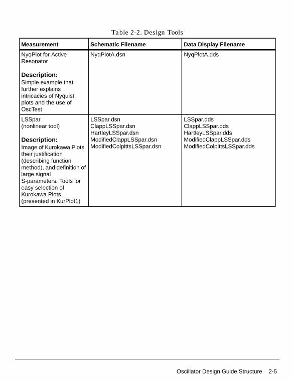
NyqPlot for ActiveResonator
Description:Simple example thatfurther explainsintricacies of Nyquistplots and the use ofOscTest
NyqPlotA.dsn NyqPlotA.dds
LSSpar(nonlinear tool)
Description:Image of Kurokawa Plots,their justification(describing functionmethod), and definition oflarge signalS-parameters. Tools foreasy selection ofKurokawa Plots(presented in KurPlot1)
LSSpar.dsnClappLSSpar.dsnHartleyLSSpar.dsnModifiedClappLSSpar.dsnModifiedColpittsLSSpar.dsn
LSSpar.ddsClappLSSpar.ddsHartleyLSSpar.ddsModifiedClappLSSpar.ddsModifiedColpittsLSSpar.dds
Table 2-2. Design Tools
Measurement Schematic Filename Data Display Filename
Oscillator Design Guide Structure 2-5

Oscillator DesignGuide Reference
Components and Component Characterization Tools
The items in the Components and Component Characterization libraries contain asmall custom library of resonators and devices, which can help in either modifying anexisting oscillator or assembling a new one. They include device DC and S-parametercharacteristics, as well as resonator and filter S-parameter andimpedance/admittance characteristics.
Table 2-3 through Table 2-5 provide schematic filenames and brief descriptions foreach component. Table 2-6 provides schematic filenames and brief descriptions foreach component characterization tool.
Available Components
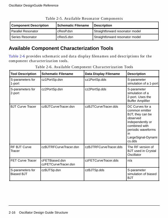
Table 2-3 provides schematic filenames and descriptions for the available activedevice components.
Table 2-3. Available Active Device Components
Component Description Schematic Filename Description
Biased BJT cBJTBiased.dsn Common Emitter BJT with a standard(1-voltage source) biasing circuit
Biased RF BJT cBJTRFBiased.dsn The RF version of BJT used in CrystalOscillator
Biased MESFET cFETBiased.dsn n/a
Varactor Diode cVar.dsn Varactor diode model, included forconvenience. Within this DesignGuide, italways appears with the reverse-biasingcircuit (see next table entry).
Biased Varactor Diode cbVar.dsn Reversed-biasing varactor
2-6 Oscillator Design Guide Structure

Table 2-4 provides schematic filenames and descriptions for the available subcircuitcomponents.
Table 2-4. Available Subcircuit Components
Component Description Schematic Filename Description
Buffer Amplifier (microwave) cAmpBuff.dsn A simple amplifier with capacitive feedbackused in frequency pull and pushsimulations, used above 2GHz (for lowerfrequencies, see below). You areencouraged to replace it by your ownamplifier and matching circuit.
Buffer Amplifier(1 - 2 MHz)
cAmpBuffS.dsn Buffer amplifier with reactive componentsadjusted for 1GHz to 2GHz range, used inSAW oscillator
Buffer Amplifier (10 - 100MHz)
cAmpBuffX.dsn Buffer amplifier with reactive componentsadjusted for 10MHz to 100MHz range, usedin crystal oscillator
Oscillator Core cOsCore.dsn Colpitts structure with a BJT with standardbias
RF Oscillator Core cOsCoreRF.dsn Oscillator Core adapted to MHz frequencyrange
Clapp Oscillator Core cClappCore.dsn Bipolar Clapp Oscillator covering afrequency range of 0.5 to 15GHz.(Other frequencies are possible bymodifying component values.)
Hartley Oscillator Core cHartleyCore.dsn Bipolar Hartley Oscillator covering afrequency range of 1 to 1000MHz(Other frequencies are possible bymodifying component values.)
Modified Clapp OscillatorCore
cModifiedClappCore Bipolar Modified Clapp Oscillator covering afrequency range of 0.7 to 7.2GHz.(Other frequencies are possible bymodifying component values.)
Modified Colpitts OscillatorCore
cModifiedCopittsCore Bipolar Colpitts Oscillator covering afrequency range of 0.8 to 6.5GHz.(Other frequencies are possible bymodifying component values.)
Fixed VSWR Complex Load cLoadEqs.dsn Load determined through VSWR andphase of the reflection coefficient
Oscillator Design Guide Structure 2-7

Oscillator DesignGuide Reference
Oscillator Core Circuits
Figure 2-1 shows the cClappCore.dsn oscillator core schematic symbol.
Figure 2-1. Bipolar Clapp Oscillator Schematic Symbol
The cClappCore.dsn oscillator operates from 0.5 to 15GHz using the existingcomponent values in the Clapp oscillator sub-circuit. Resonator tank components Ctand Lt are automatically calculated with approximations referenced to 1GHz anddisplayed on some display pages. The Ground or Series Resonator port is eitherconnected directly to ground or connected to ground through a series resonator. TheVariable Capacitance Tuning Port is used for VCO design by coupling a varactordiode across the tank capacitor Ct. Coupling is accomplished by capacitor Ccpl.Larger values of Ccpl yield tighter coupling and wider tuning range for a givenamount of tuning capacitance variation. The OscPort1 and OscPort2 ports are eitherconnected directly together or connected through a series resonator. You can connectthe OscPort test probe between these two ports for harmonic balance oscillatorsimulations. The Output Port is used for oscillator signal output. The variable Ctunesets the oscillator at the desired oscillation frequency when the capacitance acrossthe Variable Capacitance Tuning Port is equal to the Ctune set value. Figure 2-2 is anexample of the Clapp Oscillator subcircuit.
VariableCapacitanceTuning Port
Ground orconnectseriesresonator
OutputPort
OscPort2OscPort1
2-8 Oscillator Design Guide Structure

Figure 2-2. Bipolar Clapp Oscillator Subcircuit
Increase capacitors C1 and C2 for lower frequency oscillator circuits. Adjustresonator frequency offset (currently 390E6) to recenter oscillator frequency.
Oscillator Design Guide Structure 2-9

Oscillator DesignGuide Reference
Figure 2-3. Bipolar Hartley Oscillator Schematic Symbol
Figure 2-3 shows the cHartleyCore.dsn oscillator core schematic symbol. Thisoscillator operates from 1 to 1000MHz using the existing component values in theHartley oscillator sub-circuit. The resonator tank component Ct is scaled from500MHz with an approximation and displayed on some display pages. You canconnect the Ground or Series Resonator to the port directly to ground, or it can beconnected to ground through a series resonator. The Variable Capacitance TuningPort is used for VCO design by coupling a varactor diode across the tank capacitor Ct.Coupling is accomplished by capacitor Ccpl. Larger values of Ccpl yield tightercoupling and wider tuning range for a given amount of tuning capacitance variation.The OscPort1 and OscPort2 ports are either connected directly together or connectedthrough a series resonator. For harmonic balance oscillator simulations, connect theOscPort test probe between these two ports. The Output Port is used for oscillatorsignal output. The variable Ctune sets the oscillator at the desired oscillationfrequency when the capacitance across the Variable Capacitance Tuning Port is equalto the Ctune set value. Figure 2-4 shows the Hartley Oscillator subcircuit.
VariableCapacitanceTuning Port
Ground orconnectseriesresonator
OutputPort
OscPort2OscPort1
2-10 Oscillator Design Guide Structure

Figure 2-4. Bipolar Hartley Oscillator Subcircuit
Increase inductors L1 and L2 for lower frequency oscillator circuits. Adjust resonatorcapacitor Ct reference value (currently 21.3pF) to recenter oscillator frequency.
Oscillator Design Guide Structure 2-11

Oscillator DesignGuide Reference
Figure 2-5. Bipolar Modified Clapp Oscillator Schematic Symbol
Figure 2-5 shows the cModifiedClappCore.dsn oscillator core schematic symbol. ThecModifiedClappCore.dsn oscillator operates from 0.7 to 7.2GHz using the existingcomponent values in the Modified Clapp oscillator sub-circuit. Resonator tankcomponents Ct and Lt are automatically calculated with approximations referencedto 1GHz and displayed on some display pages. The Ground or Series Resonator portcan be connected directly to ground or connected to ground through a seriesresonator. The Variable Capacitance Tuning Port is used for VCO design by couplinga varactor diode across the tank capacitor Ct. Coupling is accomplished by capacitorCcpl. Larger values of Ccpl yield tighter coupling and wider tuning range for a givenamount of tuning capacitance variation. The OscPort1 and OscPort2 ports are eitherconnected directly together or connected through a series resonator. You can connectthe OscPort test probe between these two ports for harmonic balance oscillatorsimulations. The Output Port is used for oscillator signal output. Variable Ctune setsthe oscillator at the desired oscillation frequency when the capacitance across theVariable Capacitance Tuning Port is equal to the Ctune set value. Figure 2-6 showsthe Modified Clapp Oscillator subcircuit.
VariableCapacitanceTuning Port
Ground orconnectseriesresonator
OutputPort
OscPort2OscPort1
2-12 Oscillator Design Guide Structure

Figure 2-6. Bipolar Modified Clapp Oscillator Subcircuit
Increase capacitors C1 and C2 for lower frequency oscillator circuits. Adjustresonator frequency offset (currently 290E6) to recenter oscillator frequency.
Oscillator Design Guide Structure 2-13

Oscillator DesignGuide Reference
Figure 2-7. Bipolar Modified Colpitts Oscillator Schematic Symbol
Figure 2-7 shows the cModifiedColpittsCore.dsn oscillator core schematic symbol.This oscillator operates from 0.8 to 6.5GHz using the existing component values inthe Modified Colpitts oscillator sub-circuit. Resonator tank inductor Lt isautomatically calculated with an approximation and displayed on some displaypages. The Ground or Series Resonator port can be connected directly to ground orconnected to ground through a series resonator. The Variable Capacitance TuningPort is used for VCO design by coupling a varactor diode across the tank inductor Lt.Coupling is accomplished by capacitor Ccpl. Larger values of Ccpl yield tightercoupling and wider tuning range for a given amount of tuning capacitance variation.The OscPort1 and OscPort2 ports are either connected directly together or connectedthrough a series resonator. Connect the OscPort test probe between these two portsfor harmonic balance oscillator simulations. The Output Port is used for oscillatorsignal output. The variable Ctune sets the oscillator at the desired oscillationfrequency when the capacitance across the Variable Capacitance Tuning Port is equalto the Ctune set value. Figure 2-8 is the Modified Colpitts Oscillator subcircuit.
VariableCapacitanceTuning Port
Ground orconnectseriesresonator
OutputPort
OscPort2OscPort1
2-14 Oscillator Design Guide Structure

Figure 2-8. Bipolar Modified Colpitts Oscillator Subcircuit
Increase scaled 10nH inductance reference value for lower frequency oscillatorcircuits. Tank inductance Lt is scaled from 1GHz using an approximation. IncreasingC1 and C2 capacitors yields a lower frequency oscillator as well.
Table 2-5 provides schematic filenames and descriptions for the available resonatorcomponents.
Table 2-5. Available Resonator Components
Component Description Schematic Filename Description
Crystal Resonator cResXtal.dsn Straightforward resonator model
SAW Resonator cResSAW.dsn Straightforward resonator model
YIG Resonator cResYIG.dsn Straightforward resonator model
Oscillator Design Guide Structure 2-15
Oscillator DesignGuide Reference
Available Component Characterization Tools
Table 2-6 provides schematic and data display filenames and descriptions for thecomponent characterization tools.
Parallel Resonator cResP.dsn Straightforward resonator model
Series Resonator cResS.dsn Straightforward resonator model
Table 2-6. Available Component Characterization Tools
Tool Description Schematic Filename Data Display Filename Description
S-parameters for1-port
cz1PortSp.dsn cz1PortSp.dds S-parametersimulation of a 1-port
S-parameters for2-port
cz2PortSp.dsn cz2PortSp.dds S-parametersimulation of a2-port. Uses theBuffer Amplifier
BJT Curve Tracer czBJTCurveTracer.dsn czBJTCurveTracer.dds DC Curves for acommon emitterBJT, they can beobservedindependently orcombined withperiodic waveformsinLargeSignal-Dynamics.dds
RF BJT CurveTracer
czBJTRFCurveTracer.dsn czBJTRFCurveTracer.dds The RF version ofBJT used in CrystalOscillator
FET Curve Tracer cFETBiased.dsnczFETCurveTracer.dsn
czFETCurveTracer.dds n/a
S-parameters forBiased BJT
czBJTSp.dsn czBJTSp.dds S-parametersimulation of biasedBJT
Table 2-5. Available Resonator Components
Component Description Schematic Filename Description
2-16 Oscillator Design Guide Structure
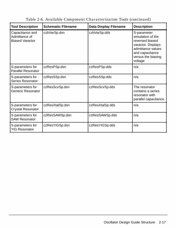
Capacitance andAdmittance ofBiased Varactor
czbVarSp.dsn czbVarSp.dds S-parametersimulation of thereversed biasedvaractor. Displaysadmittance valuesand capacitanceversus the biasingvoltage
S-parameters forParallel Resonator
czResPSp.dsn czResPSp.dds n/a
S-parameters forSeries Resonator
czResSSp.dsn czResSSp.dds n/a
S-parameters forGeneric Resonator
czResScvSp.dsn czResScvSp.dds The resonatorcontains a seriesresonator withparallel capacitance.
S-parameters forCrystal Resonator
czResXtalSp.dsn czResXtalSp.dds n/a
S-parameters forSAW Resonator
czResSAWSp.dsn czResSAWSp.dds n/a
S-parameters forYIG Resonator
czResYIGSp.dsn czResYIGSp.dds n/a
Table 2-6. Available Component Characterization Tools (continued)
Tool Description Schematic Filename Data Display Filename Description
Oscillator Design Guide Structure 2-17

Oscillator DesignGuide Reference
Generic Oscillator ExampleThe oscillator circuit for the Generic Oscillator example is set up as follows:
• Resonator
• Oscillator active part (OscCore)
• Lload, which can include buffering amplifier and matching circuits
The tools consists of three parts, as explained in the section, “Oscillator Design GuideStructure” on page 2-1.
For simplicity, we show the buffering amplifier in two designs only and don’t includethe matching circuits. The generic resonator is presented here by a series resonantcircuit shunted by a capacitance, which can model either a tuning capacitance, or theeffect of packaging.
The OsCore is the Colpitts structure, which was introduced soon after the inventionof triode (called audion at the time). It is still widely used. It uses a capacitive RFtransformer to provide feedback. The transformer capacitors together with theinductor determine the oscillation frequency f = 1/sqrt(L×C1×C2/(C1+C2)).
The Load models impedance, as seen by the OsCore component. Typically, this is theinput impedance of the buffering amplifier(s) (including matching circuits) and theactual load.
2-18 Generic Oscillator Example

Oscillator Simulation
The oscillator designs included in this DesignGuide provide easy access to observingthe nonlinear behavior of an oscillator. The circuit design for the generic example isshown in Figure 2-9. It includes fixed load, a clearly visible active circuit, and thetunable resonator separated by the OscPort component.
Figure 2-9. Structure of Oscillator Circuit
Generic Oscillator Example 2-19

Oscillator DesignGuide Reference
Single-Frequency Oscillations
The results of single-frequency oscillations in Figure 2-10 show output and resonatorvoltages. They also provide oscillations frequency, power harmonic content, thecorresponding time-domain waveform, and the values of DC power and RF outputpower.
Figure 2-10. Results of Single-Frequency Oscillations
2-20 Generic Oscillator Example

Dynamics of Single-Frequency Oscillations
The graph in Figure 2-11 shows waveforms of Collector-Emitter voltage and thecollector current of the OsCore BJT superimposed on BJT’s DC characteristics.
Figure 2-11. Dynamics of Single-Frequency OscillationFigure 2-12.
Generic Oscillator Example 2-21

Oscillator DesignGuide Reference
Single-Frequency Oscillations with Noise
The graph in Figure 2-13 shows single-frequency results with the noisecharacteristics of Vout and Vres. It also lists the components that affect the noise themost. You can specify the range after which small contributors to noise will beneglected. In this example, the range is set to 15 dB.
Figure 2-13. Single-Frequency Oscillations with Noise
2-22 Generic Oscillator Example

Frequency Pulling
Figure 2-14 shows results after the original circuit is modified for frequency pull.Changes include the varying load and a simple buffer amplifier, which was added tomake pulling values realistic. The load is specified in terms of VSWR. You candetermine the best variation. The graph shows that frequency variation for varyingphase of the load. VSWR is fixed, with its value shown above the plot. By moving themarker on the VSWR selection plot, you can obtain the results for other VSWRvalues. The corresponding load characteristic and the corresponding value of Voutfundamental are shown in the lower plots. The equation with pulling value will beadded.
Figure 2-14. Results with Circuit Modified for Frequency Pulling
Generic Oscillator Example 2-23

Oscillator DesignGuide Reference
Frequency Pushing
Figure 2-15 shows results after the frequency pull circuit is modified for frequencypush, with fixed load (vswr=1, phi =0) and varying bias on oscillator’s transistor Vcc.The display presents frequency variation with Vcc.
For Vcc=8V, the circuit does not oscillate, which results in the error message.Nevertheless, the sweep is performed, showing oscillations for higher bias. Twomarkers on the plot allow us to zoom in at the frequency plot. The plot to the right isdetermined by markers position. The corresponding value of Vout fundamental isshown in the lower plot.
Figure 2-15. Results with Circuit Modified for Frequency Pushing
2-24 Generic Oscillator Example

Tuned Oscillations
Figure 2-16 shows the resonator voltage and its harmonics. It provides the tuningcharacteristics of sweeps vs. capacitance vs. frequency.
Figure 2-16. Resonator Voltage and Harmonics
Linear Design Tools
The designs used for linear applications provide tools to investigate oscillationsconditions. They belong to two groups, as follows:
• Necessary oscillation conditions
• Check for Nyquist stability criterion, using the linearized version of the OscPortcomponent, called OscTest.
Generic Oscillator Example 2-25

Oscillator DesignGuide Reference
Load-to-Resonator Mapping
Load-to-resonator mapping is represented by the design MapLoad.dsn and the graphMapLoad.dds. The design consists of the oscillator circuit without the resonator. Thebuffer and load are replaced by varying load. The load values correspond to maintraces on a Smith chart (shown in the loadmap.dds display). You can specify thenumber of samples per trace and the radius of the small circle. On the resonator side,the circuit is terminated by an S-parameter port. S-parameter analysis is performedover frequency band determined that you specify so that the mapping can beanalyzed at various frequencies.
The purpose of the analysis is to observe how the different values of the load will bedetected by the resonator. The values that map outside the unit circle are ofparticular interest. These are the values that will provide negative resistance facingthe resonator, so that the necessary oscillations conditions will be satisfied
The graph MapLoad.dds, as shown in Figure 2-17, represents load values and theirimage in the resonator plane. Color-coded markers facilitate orientation. The markeron the bottom plot selects frequency at which the mapping is performed.
2-26 Generic Oscillator Example

Figure 2-17. Load Values and Their Image in Resonator Plane
Generic Oscillator Example 2-27

Oscillator DesignGuide Reference
Resonator-to-Load Mapping
Resonator-to-load mapping is represented by the design MapInput.dsn and the graphMapInput.dds, as shown in Figure 2-18. The design is dual to load-to-resonatormapping, and it determines the image of the resonator at the buffer amplifier input.Consequently, it is useful in designing of the amplifier matching circuit. A specialcase restricted to a unit circle input gave rise to the method of stability circles (seeReference 1 in the section “Bibliography” on page 2-42).
Figure 2-18. Resonator-to-Load Mapping
2-28 Generic Oscillator Example

Stability Via Nyquist Plots
The design Nyquist Stab shows the use of the OscTest component. The results shownfor different choices of the OscTest characteristic impedance Zo illustrate theimportance of the Nyquist plot. Zo is swept from 1.5ohm to 21.5 ohm in 10 steps. Theplots clearly show that it is the encirclement of 1+j0 that matters (as we know fromthe Nyquist theorem) and not the value of S11 at the crossing of the real axis. Thejustification of this statement is illustrated by two simple designs (NyqStab,NyqStabA) described in the next section.
Figure 2-19. Resonator-to-Load Mapping
Generic Oscillator Example 2-29

Oscillator DesignGuide Reference
Theory of Stability vs. Nyquist Plots
There is a widespread belief [3,7,9,10,11,12,13,14,15] that the stability of oscillatorscan be determined by a particular criterion. When the phase of the transfer functionis zero and the magnitude (at the same frequency) is larger than one, the system isunstable. The circuit shown in the criterion is usually presented as two equations:
arg(Sn) = – arg(Sr), | Sn Sr | > 1
Consider a simplest possible linearized oscillator, as shown in Figure 2-20. Thecircuit has the resonator's resistance rr=1/G = 100.0 ohm and the active (linearized)resistance ra = 1/g'(Vo) = –5.0 ohm and is obviously unstable.
Figure 2-20. Stability Via Nyquist Plots
The Nyquist plots and equation were checked for different values of the characteristicimpedance Zo. The system stability depends on the position of poles of the transferfunction Sr(s)Sn(s). If the function possesses poles in the right half plane, the systemis unstable. It follows from the Nyquist criterion that the presence of poles in theright-half plane and the system instability can be determined by the encirclements ofpoint 1+j0 by the osctest generated contour S11 = Sr(jw)Sn(jw).
The Nyquist plots obtained for Zo = 2.0, 82.0, 162.0 ohm are shown in Figure 2-21.
2-30 Generic Oscillator Example

Figure 2-21. Nyquist Plot for Simple Linearized Oscillator
The three values of Zo are chosen so that we get respectively:
Zo < |ra| < rr, |ra| < Zo < rr
and
|ra| < rr < Zo
The circuit is obviously unstable. Consequently, the Nyquist loop, shown in the plotson the left in Figure 2-22, encircles the point 1+j0 for every value of Zo. However, ifwe turn to the magnitude-phase plots (shown to the right), then the circuit instabilitywill be hard to deduce. Finally the intuitive condition (1) ( SnSr >1 for arg(SnSr) = 0)obviously fails for Zo = 82.0 and Zo=162.0 ohm.
Generic Oscillator Example 2-31

Oscillator DesignGuide Reference
The SrSn contours clearly show that it is the encirclement of 1+j0 that matters (aswe know from Nyquist theorem) and not the value of SnSr at the crossing of the realaxis.
The Nyquist criterion is most useful when the open loop system is stable. In thatcase, the stability of the feedback system is determined by the closing of the feedbackloop. Figure 2-22 shows a variation of our original circuit.
Figure 2-22. Nyquist Plot for Simple Circuit
2-32 Generic Oscillator Example

In the circuit shown, the resistances were interchanged, resulting in an activeresonator, for which adding the 100 ohms in parallel (i.e. loop closing) does notchange its instability. Obviously, in this system, the Nyquist loop does not encircle the1+j0. This is because the open loop transfer function Yn Zr = (s/rrC)/(s^2 +s/raC+ 1/LC) has two poles in the right half plane and loop closing does not add any newpoles.
Therefore the position of the OscTest probe (which automatically computes SrSn inthe simulator) should be carefully chosen. It should be placed between the resonatorand the active circuit so that the open-loop system is stable.
The plots of S11 for Zo = 2.0,82.0,162.0 need to be considered.For Zo = 82.0, 162.0 theNyquist loop does not encircle 1+j0, as expected. However, for Zo=2.0 it does, whichseems contrary to the fact that the resonator circuit is active. The explanation for thisis that the open loop S-parameter transfer function:
Sr(s) = (Zr – Zo)/(Zr + Zo) = –(s^2+ s((1/ra)–(1/Zo))/C+1/LC)/(s^2+ s((1/ra)+(1/Zo))/C+1/LC)
has all poles in the left hand plane for Zo<|ra|. Only closing the loop makes thesystem unstable.
Generic Oscillator Example 2-33

Oscillator DesignGuide Reference
Using Nonlinear Design Tools
Figure 2-23. Large-Signal S-Parameter Design
In the steady-state, because of intrinsically nonlinear behavior of oscillators, signalsare no longer sinusoidal. Consequently, the concepts of impedance and S-parametersare not obvious. However, in high-Q circuits, in which signals are represented bytheir fundamental components, there is a natural way to define the large-signalimpedance, or large-signal S-parameters. In this section, we define the large signalS-parameters and demonstrate that the equations
arg(Sn) = – arg(Sr)| Sn Sr | = 1
determine amplitude and phase of oscillations.
2-34 Generic Oscillator Example

The steady state periodic oscillations can be represented by their Fourier series:
v(t) = ∑ |vn| cos(nωt + ϕn) i(t) = ∑ |in| cos(nωt + ψn)
For a high-Q resonator the higher harmonics are negligibly small and voltage andcurrent can be approximated by:
v(t) ≈ |V| cos(ω t + ϕ)
i(t) ≈ |I| cos(ω t + ψ)
where
V = |V| exp(jϕ), and I = |I| exp(jψ)
denote the fundamental components of voltage and current.
Thus the signals are represented by their complex amplitudes V and I, for which wedefine the large-signal incident and reflected waves:
a = (V + Zo×I)/(2√Zo), b = (V – Zo×I)/(2 √Zo)
On the resonator side, we have a = Sr b, with b = b(a) on the active circuit side. Thesetwo relationships provide us with the steady-state equations a = Sr b(a). Afterdefining the large signal S-parameter: Sn = b(a)/a the steady state equation can berepresented as a = Sr Sn a, which leads to: 1 = Sr Sn, which is equivalent to theequations.
Solving Harmonic Balance Convergence ProblemsHarmonic balance simulation in Advanced Design System is an excellent way toanalyze many oscillators in the frequency domain. Occasionally, you might have anoscillator that converges in a time-domain simulation, but the harmonic balanceoscillator algorithm is unable to find the solution. There are two techniques in ADSfor solving those oscillators:
• Analyzing the large-signal loop gain in harmonic balance to find the point ofoscillation and using that as an initial guess for the full harmonic balanceoscillator analysis
• Using a transient analysis to produce an initial guess for harmonic balanceoscillator analysis.
In the DesignGuide > Oscillator menu, select Solving Harmonic Balance ConversionProblems for several useful design examples.
Solving Harmonic Balance Convergence Problems 2-35

Oscillator DesignGuide Reference
For more information on these techniques, refer to the ADS Circuit Simulationmanual, in the section “Simulation Techniques for Recalcitrant Oscillators, inChapter 9, “Harmonic Balance for Oscillator simulations.
Oscillator Core ExamplesOscillator Cores (cClappCore, cHartleyCore, cModifiedClappCore, andcModifiedColpittsCore) are compatible with simulation and measurement setupsoutlined by the Generic Oscillator Example. These core oscillator circuits areconfigured for low resistance loads. (50ohm is used for these four oscillator cores,although other load values are possible.) The design and display filenames for theseexamples follow a naming convention that indicates oscillator type and simulationsetup as follows:
• OscillatorTypeSimulationType.dsn
• OscillatorTypeSimulationType.dds
where:
OscillatorType indicates one of the following topologies: Clapp, Hartley, ModifiedClapp, or Modified Colpitts.
SimulationType provides one of the following simulation set-ups or measurements:FixedFreqOsc, FreqPull, FreqPush, FreqTune, LSSpar, MapInput, MapOutput,NyqStab, or Phase Noise.
For example, the simulation that determines oscillator frequency of a Clapp oscillatorhas the design filename ClappFixedFreqOsc.dsn and a data display filenameClappFixedFreqOsc.dds. This simulation predicts oscillation frequency, output power,and calculates tank components Lt and Ct. The accompanying data display presentsthese results.
The cClappCore circuit is used to illustrate available simulation setups offered in thedesign guide.
2-36 Oscillator Core Examples

Figure 2-24. Oscillator Core Circuit Simulation Connections
Figure 2-24 shows the Clapp oscillator harmonic balance simulationClappFixedFreqOsc.dsn that determines oscillation frequency, output power and tankcomponent values at 1GHz. The OscPort probe is shown connected between the activedevice and tank resonator. Resonator tank components Lt and Ct are computed andshown on the companion data display page.
Oscillator Core Examples 2-37

Oscillator DesignGuide Reference
Oscillator Core Series Resonator Connection Alternatives
Oscillator core circuits (cClappCore, cHartleyCore, cModifiedClappCore, andcModifiedColpittsCore) are compatible with series resonators in two ways.
Figure 2-25. Series Resonator Connection Between Tank and Active Circuit
The first possibility shown by Figure 2-25 connects the series resonator between thetank circuit and active device. If resonator losses are low, the series resonator canalso be connected between the bipolar base terminal and ground as shown inFigure 2-26.
2-38 Oscillator Core Examples

Figure 2-26. Series Resonator Connection Transistor Base and Ground
Oscillator Core Examples 2-39

Oscillator DesignGuide Reference
Additional Examples
Following are examples in addition to the primary example, as described in thesection, “Generic Oscillator Example” on page 2-18.
The design and display filenames for these examples follow the generic oscillatornaming convention with 3-letter prefixes attached to the generic names, as follows:
• xxxgenericoscillator name.dsn
• xxxgenericoscillator name.dds
where xxx stands for one of: saw, vco, xto, or yto.
For example, VCO Large Signal S-Parameters have the filenames vcoLSSpar.dsn andvcoLSSpar.dds.
Crystal Oscillator (XTO)
These oscillators are notable for their high frequency stability and low cost. Typicalstructure is that of a Colpitts oscillator with quartz crystal resonator introduced intofeedback path. Mechanical vibrations of the crystal stabilize the oscillationsfrequency. Vibration frequency is sensitive to temperature. Therefore, temperaturecompensation circuits are often used to improve frequency stability. Crystalresonators are typically used in the range up to 100 MHz (to a few hundreds of MHzif resonating on overtones).
SAW Resonator Oscillator (SAW)
Principle of operation is similar to that of crystal oscillator with the quartz resonatorreplaced by a Surface Acoustic Wave oscillator. SAW resonators are used in frequencyrange up to 2 GHz.
Voltage Controlled Oscillator (VCO)
In any of the preceding structures, frequency tuning can be provided by adding avaractor diode to the resonator. The varactor diode serves as a voltage controlledcapacitor. It has very fast tuning speed (GHz/nsec) and low Q. Consequently, thevaractor can be used with LC elements to provide wide tuning (with poor frequencystability) or with a crystal, SAW or DRO resonator for narrow tuning with betterfrequency stability.
2-40 Oscillator Core Examples

At microwave frequencies, the device capacitances become significant, resulting in adifferent (often simpler) circuit. The operation principles, remain the same.
YIG Tuned Oscillator (YTO)
For a very wide band (that can reach decade) tuning with high frequency stabilityand for frequency range of 1 GHz to 50 GHz. YIG (Yttrium-Iron-Garnett) resonatorsare used. The YIG sphere behaves like a resonator with 1000-to-8000 unloaded Qresulting in very good frequency stability. The resonator are tunable over widebandwidth with excellent linearity (~0.05%). For fine tuning (for phase-lock), orfrequency modulation an FM coil can be added.
Oscillator Core Examples 2-41

Oscillator DesignGuide Reference
Bibliography[1]G.R.Basawapatna, R.B.Stancliff, “A Unified Approach to the Design of
Wide-Band Microwave Solid State Oscillators,” IEEE Trans. MTT-27, May1979, pp 379-385.
[2] Fundamentals of Quartz Oscillators” HP Application Note 200-2.
[3] R. T. Jackson, “Criteria for the Onset of Oscillations in Microwave Circuits,”IEEE Trans. MTT-40, Mar 1992, pp 566-568, “Comments on ``Criteria...,'' IEEETrans. MTT-40, Sept 1992, pp1850-1851.
[4] A. P. S. Khanna, “Oscillators” in Chapter 9 of “Microwave Solid State CircuitDesign” by I. Bahl P. Bhartia, J.Wiley 1988.
[5] Khanna and Obregon - “Microwave Oscillator Analysis” - IEEE Trans.vol.MTT-29, June 1981, pp 606-607.
[6] M.Odyniec, “Nonlinear Synchronized LC Oscillators, Theory and Simulation,”IEEE Transactions, MTT-41, May 1993, pp 774-780.
[7] M.Odyniec, “Benchmarks for Nonlinear Simulation,” APMC'94, Tokyo, Japan,Dec. 6-9 1994.
[8] M.Odyniec, “Stability Criteria via S-parameters,” EUMC'95, Bologna, Italy,Sept. 4-8, 1995.
[9] V.Rizzoli, F. Mastri, and D, Maroti, “General noise analysis,” IEEE Trans.MTT-37, Vol.1, No. 1, January 1989.
[10] C. Schiebold, “Getting Back to the Basics of Oscillator Design,” MicrowaveJournal, May 1998.
[11] J.C. Slater, “Microwave Electronics,” Van Nostrand, Princeton, 1950.
[12] “S-parameter Design,” HP Application Note 159.
[13] A. Sweet, “MIC and MMIC Amplifier and Oscillator Circuit Design,” ArtechHouse, Boston 1990.
[14] D. Warren et al., “Large and Small Signal Oscillator Analysis,” MicrowaveJournal, May 1989.
[15] J.J. D'Azzo, C. H. Houpis, “Feedback Control Systems,” McGraw-Hill New York1960.
2-42 Bibliography

[16] J. W. Boyles, “The Oscillator as a Reflection Amplifier...” Microwave Journal,June 1986.
[17] J.L.J. Martin and F.J.O.Gonzalez, “Accurate Linear Oscillator Analysis andDesign,” Microwave Journal, June 1996.
[18] Z. Nativ and Y. Shur, “Push-Push VCO Design with CAD Tools. “
[19] Microwave Journal, February 1989.
[20] M. Odyniec, “Stability Criteria via S-parameters “European MicrowaveConference, Bologna, Italy, September 1995.
[21] A. Przedpelski, “Simple, Low Cost UHF VTOs “RF Design,” May 1993.
[22] N. Ratier et al. “Automatic Formal Derivation of the Oscillation Condition”,IEEE Int. Frequency Control Symp. 1997.
[23] T. Razban et al.,”A Compact Oscillator...” Microwave Journal, February 1994.
[24] S. Savaria and P. Champagne, “Linear Simulators...” Microwave Journal, May1995.
Selected Papers
[25] Basawapatna and Stancliff - “A Unified Approach to the Design of WidebandMicrowave Solid State Oscillators” - IEEE trans. vol MTT-27, May 1979, pp379-385.
[26] Khanna and Obregon - “Microwave Oscillator Analysis” - IEEE Trans. vol.MTT-29, June 1981, pp 606-607.
[27] M.Odyniec, “Nonlinear Synchronized LC Oscillators, Theory and Simulation,”IEEE Transactions, MTT-41, May 1993, pp 774-780.
[28] M.Odyniec, “Benchmarks for Nonlinear Simulation,” APMC'94, Tokyo, Japan,Dec. 6-9 1994.
[29] M.Odyniec, “Stability Criteria via S-parameters,” EUMC'95, Bologna, Italy,Sept. 4-8, 1995.
Bibliography 2-43

Oscillator DesignGuide Reference
2-44 Bibliography

Index
DDesignGuide QuickStartsOscillator, 1-1
OOscillator DesignGuide
bibliography, 2-42component characterization tools, 2-16component menus, 1-5components, 2-6design flow example, 1-9design tools, 2-4examples
Crystal, 2-40generic, 2-18SAW Resonator, 2-40voltage control, 2-40YIG-tuned, 2-41
linear design tools, 2-25load-to-resonator mapping, 2-26main menu, 1-5nonlinear measurements, 2-2QuickStart, 1-1Reference, 2-1resonator-to-load mapping, 2-28stability vs. Nyquist plots, 2-29structure, 2-1
Index-1

Index-2