
Optoelectronics Department - Ulm · a continuous output power of 3.6W in single spatial mode...
114
ANNUAL REPORT 2004 Optoelectronics Department U N I V E R S I T Ä T U L M · S C I E N D O · D O C E N D O · C U R A N D O · University of Ulm
Transcript of Optoelectronics Department - Ulm · a continuous output power of 3.6W in single spatial mode...

ANNUAL REPORT 2004
Optoelectronics
DepartmentU
N
IVERSI TÄ T
ULM·
SC
IEN
DO
·DOCENDO·C
UR
AN
DO
·
University of Ulm


Contents I
Contents
Preface . . . . . . . . . . . . . . . . . . . . . . . . . . . . . . . . . . . . . . . . . 1
Articles
Lensed Top-Emitting VCSELs . . . . . . . . . . . . . . . . . . . . . . . . . . . . 3
High-Power VCSELs With One Preferred Polarization . . . . . . . . . . . . . . 9
M2 Measurements of High-Power VCSELs . . . . . . . . . . . . . . . . . . . . . 17
2-D 850 nm VCSEL Arrays With Redundant Pixel Designs . . . . . . . . . . . . 21
High-Performance Low-Cost Optical Link at 850 nm . . . . . . . . . . . . . . . . 27
40Gbit/s Operation of Laser-Integrated Electroabsorption Modulator . . . . . . 31
Investigation of the Capacitance of Integrated DFB–EAMs . . . . . . . . . . . . 37
HVPE of Thick GaN . . . . . . . . . . . . . . . . . . . . . . . . . . . . . . . . . 41
GaN FACELO Structures With Marker Layers . . . . . . . . . . . . . . . . . . . 45
Epitaxial Growth of AlGaN Layers . . . . . . . . . . . . . . . . . . . . . . . . . 51
InGaN QWs Grown on Facets . . . . . . . . . . . . . . . . . . . . . . . . . . . . 55
Longitudinal Mode Patterns in GaInN Lasers . . . . . . . . . . . . . . . . . . . 59
MBE Growth of GaNAs and AlGaNAs Layers . . . . . . . . . . . . . . . . . . . 65
Strain Compensated Disk Lasers Structures . . . . . . . . . . . . . . . . . . . . 71
Semiconductor Disk Laser on Microchannel Cooler . . . . . . . . . . . . . . . . 79
Optimization of Process Parameters for Low-Absorbing Optical Coatings . . . . 85
External-Cavity Tapered Semiconductor Ring Lasers . . . . . . . . . . . . . . . 91
Lists of Publications
Ph.D. Theses . . . . . . . . . . . . . . . . . . . . . . . . . . . . . . . . . . . . . 97
Diploma and Master Theses . . . . . . . . . . . . . . . . . . . . . . . . . . . . . 98
Semester Projects . . . . . . . . . . . . . . . . . . . . . . . . . . . . . . . . . . . 100
Talks . . . . . . . . . . . . . . . . . . . . . . . . . . . . . . . . . . . . . . . . . . 101
Publications and Conference Contributions . . . . . . . . . . . . . . . . . . . . . 103

II Annual Report 2004, Optoelectronics Department, University of Ulm

Staff III
1: Rainer Blood 2: Johannes M. Ostermann 3: Peter Bruckner4: Martin Stach 5: Frank Habel 6: Christoph Kirchner7: Josef Theisz 8: Jurgen Mahnß 9: Rainer Michalzik10: Hildegard Mack 11: Hendrik Roscher 12: Gerlinde Meixner13: Barbara Neubert 14: Peter Unger 15: Frank Demaria16: Philipp Gerlach 17: Steffen Lorch 18: Rudolf Rosch19: Ihab Kardosh 20: Eckart Gerster 21: Ferdinand Scholz22: Michael C. Riedl 23: Andrea Kroner 24: Fernando Rinaldi25: Manmohan S. Shishodia
Missing in the picture
26: Christine Bunk 27: Karl J. Ebeling 28: Daniel Hofstetter29: Sukran Kilic 30: Susanne Menzel 31: Georgi Stareev

IV Annual Report 2004, Optoelectronics Department, University of Ulm
Optoelectronics DepartmentUniversity of Ulm
Albert-Einstein-Allee 45, D-89081 Ulm, GermanyURL:Fax:Phone:
http://www-opto.e-technik.uni-ulm.de+49–731/50–260 49+49–731/50–
Head of DepartmentProf. Dr. Peter Unger –2 60 54 [email protected]
Deputy HeadProf. Dr. Ferdinand Scholz –2 60 52 [email protected]
President of the University of UlmProf. Dr. Karl Joachim Ebeling –2 60 51 [email protected]
Senior Research AssistantDr.-Ing. Rainer Michalzik –2 60 48 [email protected]
Cleanroom ManagementDr.-Ing. Jurgen Mahnß –2 60 53 [email protected]
SecretariesChristine Bunk –2 60 50 [email protected]
Sukran Kilic –2 60 51 [email protected]
Hildegard Mack –2 60 59 [email protected]
Guest ScientistDr. Daniel Hofstetter –2 60 51 [email protected]
M. Tech. Manmohan S. Shishodia∗ –2 60 36 [email protected]
Research StaffDipl.-Ing. Peter Bruckner –2 60 35 [email protected]
Dipl.-Phys. Frank Demaria –2 60 46 [email protected]
Dipl.-Ing. Christoph Eichler∗ –2 61 95 [email protected]
Dipl.-Ing. Philipp Gerlach –2 60 37 [email protected]
Dipl.-Ing. Eckart Gerster∗ –2 60 57 [email protected]
Dipl.-Ing. Frank Habel∗ –2 64 52 [email protected]
Dipl.-Ing. Ihab Kardosh –2 60 36 [email protected]
Dr.-Ing. Christoph Kirchner –2 60 35 [email protected]
Dipl.-Ing. Andrea Kroner –2 60 38 [email protected]
Dipl.-Ing. Steffen Lorch –2 60 39 [email protected]
Dipl.-Phys. Manfred Mundbrod∗ –2 60 39 [email protected]
Dipl.-Ing. Barbara Neubert –2 64 54 [email protected]
Dipl.-Phys. Johannes M. Ostermann –2 60 38 [email protected]
Dipl.-Ing. Michael C. Riedl –2 60 36 [email protected]
Dipl.-Phys. Fernando Rinaldi –2 60 46 [email protected]

Staff V
Dipl.-Ing. Hendrik Roscher –2 60 44 [email protected]
Dipl.-Ing. Sven-Silvius Schad∗ –2 61 95 [email protected]
Dipl.-Ing. Martin Stach –2 60 37 [email protected]
Dr.-Ing. Georgi Stareev –2 64 53 [email protected]
Technical StaffRainer Blood –2 60 44 [email protected]
Gerlinde Meixner –2 60 41 [email protected]
Susanne Menzel –2 60 41 [email protected]
Josef Theisz –2 60 30 [email protected]
∗ Member has left the department meanwhile

VI Annual Report 2004, Optoelectronics Department, University of Ulm

Preface 1
Preface
During 2004, the research activities of the Optoelectronics Department have been contin-uing in the areas of optical interconnect systems, vertical-cavity surface-emitting lasers,GaN-based electronic and optoelectronic devices, optically pumped semiconductor disklasers, and high-power semiconductor amplifiers. Main achievements of the VCSELs andOptical Interconnects Group headed by Rainer Michalzik are first 40Gbit/s signals gener-ated by a 1300 nm InGaAlAs/InP-based DFB laser monolithically integrated with an elec-troabsorption modulator, flip-chip bonded two-dimensional 850 nm VCSEL arrays withthreefold functional redundancy and down to 13.5µm device pitch, as well as polarization-stable, high single- and multimode output power VCSELs incorporating specially tailoredsurface gratings. In the GaN Electronics and Optoelectronics Group headed by Ferdi-nand Scholz, high quality GaN layers could be grown by optimizing a multi-step growthprocedure by the aid of marker layers. This together with our optimized HVPE processbrought us closer to the realization of GaN wafers regarded as prerequisites for long-livingshort-wavelength laser diodes. Moreover, our investigations in modelling, mounting, andcharacterization of laser diodes helped to achieve new records in device lifetime by ourproject partners. In the High-Power Semiconductor Laser Group headed by Peter Unger,a continuous output power of 3.6W in single spatial mode operation has been achievedwith a semiconductor disk laser.
Four members of the Department, namely Irene Ecker, Marcus Scherer, Matthias Golling,and Jurgen Joos received their Ph.D. degrees. Furthermore, 11 Diploma or Master Thesesand 5 Semester Projects have been carried out in 2004.
The Department further intensified the close collaboration with industrial partners. Wealso appreciate the financial support of national and European research organizations,which contribute the major part of our funding. Numerous publications at internationalconferences and a large number of articles in respected journals document the strongresearch activities of the Department. A detailed list can be found at the end of thisreport.
Peter Unger Ulm, August 2005

2 Annual Report 2004, Optoelectronics Department, University of Ulm

Lensed Top-Emitting VCSELs 3
Integrated Focusing Photoresist Microlenses
on AlGaAs Top-Emitting VCSELs
Andrea Kroner
We present 850 nm wavelength top-emitting vertical-cavity surface-emitting lasers(VCSELs) with integrated photoresist microlenses placed directly on the laser facet, withthe intention to focus the output beam to some micrometer beam waist in a distanceof at least 30µm. Calculations lead to necessary radii of curvature in the range of 20 to40µm, depending on the diameter of the active region. The lenses are made of polymethyl-glutarimide (PMGI) and are fabricated by a thermal reflow process which was studied atdifferent structure sizes and surface materials. Finally, basic measurements on first de-vices are presented.
1. Introduction
Microlenses have become an important component in many modern optical systems likeoptical disk players or fiber coupling setups. Nowadays, various fabrication techniquesfor microlenses are known and used, e.g., microjet printing, reflow processes or grey-scalelithography [1]. In the past years, different approaches have been presented to integrateVCSELs and microlenses to small-sized systems in order to shape the laser output beam[2], [3]. In most cases, the lenses were used to collimate the beam or at least to decrease itsdivergence. Here we present the use of photoresist microlenses to focus the output beamof top-emitting VCSELs to a desired diameter of the focal point of 4µm at the mostand a working distance of at least 30µm. Figure 1 shows a schematic of the structure,where the lens is placed directly onto the p-contact ring of the VCSEL. On one side, thep-contact ring is connected to a bondpad, so the lens also has to cover this overlap regionwith the resulting difference in height.
Output beam
MicrolensBondpadPassivation
P−contact ring
VCSELFig. 1: Schemetic structure of the VCSELwith integrated microlens.

4 Annual Report 2004, Optoelectronics Department, University of Ulm
2. Design and Fabrication of Photoresist Microlenses
To calculate the necessary lens parameters, a Gaussian laser output beam was assumed.The shape of the beam and its propagation was calculated using the so-called matrixmethod, where every optical element, like interfaces or lenses, can be described by atransfer matrix [4]. Figure 2 shows the output beams of lensed VCSELs with an emissionwavelength of 850 nm. On the left side, the internal beam waist, located at the oxideaperture, is assumed to have a diameter of 14µm and a distance to the surface of 4µm.The microlens on the surface of the VCSEL with a focal length of 50µm in air focusesthe beam to a waist of 3.7µm at a working distance of 46.5µm. On the right side, theinternal beam waist is reduced to a diameter of 10µm. To preserve an output beam waistof 4µm at the most, the focal length of the microlens has to be decreased to 40µm, whichalso lowers the working distance to 33.8µm. Therefore, aiming for active diameters of 10to 20µm, the focal length of the lenses has to cover a range of 40 to 70µm.
0 20 40 60 80 100−8
−4
0
4
8
Distance (µm)
Bea
m w
aist
(µm
)
f=50 mµ
Lensed facet
0 20 40 60 80 100−8
−4
0
4
8
Distance (µm)
Bea
m w
aist
(µm
)mµf=40
Lensed facet
Fig. 2: Calculation of the output beam of lensed VCSELs. The left side represents a lensedVCSEL with a 14 µm active diameter and a focal length of f = 50 µm. On the right side, activediameter and focal length are reduced to 10 µm and 40 µm, respectively.
The microlenses were fabricated by a thermal reflow process and are made of PMGI, apositive photoresist which is photosensitive in the deep ultraviolet (DUV) regime. PMGIresist is transparent in the near infrared and shows a smooth reflow behavior at tem-peratures above 250 C. Furthermore it shows an above-average chemical and mechanicalstability compared to other resists, so it has been used as microlens material in thepast [2].
During the process, the PMGI resist is exposed by a DUV flood exposure where nolithographic masks can be used, so a two layer process has to be applied. Therefore, afterspinning and prebaking the PMGI resist, a second resist layer (AZ1512 HS) is spun onthe wafer (see Fig. 3a). After a second prebake, this resist can be structured by contactlithography with a glass mask (Fig. 3b). It is important to note that the subjacent PMGIlayer is not affected by the AZ developer. In the following flood exposure step, the AZlayer masks the unexposed areas (Fig. 3c). Since the AZ resist is not solved by the PMGIdeveloper (Fig. 3d) it has to be removed with cold acetone, which does not affect thePMGI structures (Fig. 3e).
Afterwards, the sample is placed on a hot-plate at a temperature of more than 250 C,where the cylindrical photoresist “islands” start to melt. Due to the surface tension, the

Lensed Top-Emitting VCSELs 5
AZ−resistPMGI
Substrate a) b) c)
d) e) f)
Fig. 3: Basic steps of the microlens fabrication process.
shape of the cylinders changes in order to minimize the surface energy (Fig. 3f). Theresulting structure is in good approximation spherically shaped and has a focal length inair of
f =R
n − 1, (1)
where n is the refractive index of the PMGI resist, given as 1.535 at a wavelength of850 nm. To reach the intended focal lengths, the radii of curvature R have to be in therange of 20 to 40µm.
Assuming that the bottom diameter as well as the volume of the resist do not changeduring the reflow process, the resulting radius of curvature is only determined by theheight and the diameter of the resist islands before the reflow [1]. Figure 4 shows theradius of curvature in dependence on the lens diameter for different resist thicknesses Hs.For the present VCSEL structures, the diameter of the lens has to be in the range ofabout 10 to 40µm, otherwise it would be smaller than the output facet or larger than themesa, respectively. Therefore, an initial resist thickness of about 2µm is best suited tocover the interesting radius of curvature range.
0 10 20 30 400
20
40
60
80
Diameter (µm)
Rad
ius
of c
uvat
ure
(µm
)
0.5µm 1.0µm
1.5µm
2.0µm 2.5µm 3.0µm
Hs
Fig. 4: Radius of curvature versus thediameter of the resist islands for differ-ent initial resist thicknesses Hs underthe assumption that resist volume anddiameter do not change during the re-flow.
3. Microlens Fabrication Results
In Fig. 5 an optical microscope picture of a PMGI microlens on GaAs substrate with adiameter of 28µm and an inital resist thickness of 1.8µm can be seen. The concentricinterference lines, so-called Newton rings, arise due to interference at thin layers and

6 Annual Report 2004, Optoelectronics Department, University of Ulm
µm
1020
30
0
4
µm
−20 −10 0 10 20
0
0.5
1
1.5
2
2.5
3
Distance x (µm)
Hei
ght h
(µm
)
Spherical Fit: H=2.82 µm D=28.2 µm R=36.8 µm
AFMFit
Fig. 5: PMGI microlens on GaAs sub-strate with a diameter of 28 µm (top left),AFM measurement of the height profile (topright), and a cross-section with a sphericalfit (bottom left).
indicate the spherical shape of the lens. In the upper right corner a three-dimensionalplot of the height profile measured by an atomic force microscope (AFM) is depicted.The bottom left side shows the cross-section of the profile in the center of the lens. Thedashed line represents a spherical fit which reveals the nearly ideal spherical shape of thelens with a radius of curvature of 36.8µm.
To study the reflow process more in detail, lenses with different diameters were fabricatedat reflow temperatures of 250 C and 270 C. Furthermore, GaAs as well as gold wasexamined as surface material, with the latter being of special interest since the lenseswill be placed directly onto the p-contact ring in the final structure. Figure 6 showsthe measured radii of curvature for reflow temperatures of 250 C and 270 C, where thereflow time was kept constant at 20min. The initial resist thickness for the structures ongold as well as on GaAs was 2.0µm, so the results can be directly compared. The solidline describes the ideal behavior that was already shown in Fig. 4. For all structures amismatch to this ideal curve can be observed, which is partly caused by a decrease of theresist volume during the reflow process due to evaporation of the solvents. This decreasewas found to be in the range of 10 to 17% for all structures, where no dependence onstructure size was observed. The mean value for the sample with gold was found to beslightly smaller.
However, this could not explain the strong deviation that arises for the structures on gold,especially for small diameters and higher temperatures. Here, the radius of curvature is
Lensed Top-Emitting VCSELs 7
10 15 20 25 30 35
10
20
30
40
Initial diameter (µm)
Rad
ius
of c
urva
ture
(µm
) Gold, 250°CGold, 270°CGaAs, 250°CGaAs, 270°Cideal
a)10 15 20 25 30 35
1
1.1
1.2
1.3
1.4
Initial Diameter (µm)
Fin
al−
to−
initi
al d
iam
eter
rat
io Gold, 250°CGold, 270°CGaAs, 250°CGaAs, 270°CExponential fit
b)
Fig. 6: Measured radii of curvature (left) and ratios between final and inital lens diameter(right) for different surfaces and reflow temperatures.
larger than expected since the diameter at the bottom of the lens does not remain constantas expected, but increases by a factor of up to 1.4 during the reflow (see right side of Fig. 6).These measurements indicate a difference in wetting between PMGI resist on GaAs andgold, where the wetting on gold seems to be stronger. However, the desired radius ofcurvature range can be still covered.
4. Integration of Microlenses on Top-Emitting VCSELs
The left side of Fig. 7 shows a PMGI lens with a diameter of 20µm placed on the outputfacet of a top-emitting VCSEL. It can be seen that the lens does not only cover parts ofthe p-contact ring, but on one side also the overlap of p-contact and bond pad, which isabout 200 nm thick. However this has no significant influence on the spherical shape ofthe lens, which can be seen in the AFM measurement of the cross-section in Fig. 7 (right).
−15 −10 −5 0 5 10 15
0
0.5
1
1.5
2
2.5
3
Distance (µm)
Hei
ght (
µm)
Spherical Fit: H=2.63 µm D=20.4 µm R=21.0 µm
AFMFit
Fig. 7: PMGI microlens with a diameter of 20 µm on the output facet of a top-emitting VCSEL(left) and AFM-measured cross-section with a spherical fit (right).

8 Annual Report 2004, Optoelectronics Department, University of Ulm
0 5 10 150
1
2
3
4
5
6
Current (mA)
Opt
ical
pow
er (
mW
)
0
1
2
3
4
5
Vol
tage
(V
)
With microlensWithout microlens
Fig. 8: Operation characteristics of aVCSEL with an oxide aperture of 5.5 µmbefore and after a PMGI lens was placedon its output facet. Due to the reduc-tion of the mirror reflectivity, thresholdcurrent as well as output power have in-creased.
Figure 8 shows typical output characteristics of a VCSEL before and after a PMGI lenswas placed on is output facet. The lens has a radius of curvature of 25µm and the VCSELhas an oxide aperture of 5.5µm. Here, an increase of the threshold current as well as ofthe maximum of output power can be observed. This indicates a reduction of the uppermirror reflectivity due to the lens material. However, the integration of the photoresistmicrolens does not lead to any significant performance degradation.
5. Conclusion
With PMGI photoresist subjected to thermal reflow, it is possible to deposit almost ideallyshaped microlenses on top-emitting VCSELs. We have achieved radii of curvature in therange of 15 to 40µm on GaAs as well as on gold surfaces, where a stronger wetting ofresist on gold was observed. First measurements on lensed VCSELs show only a slightchange of threshold current and output power. In the next step, the effects on the outputfield of the laser have to be determined.
References
[1] S. Sinzinger and J. Jahns, Microoptics. Weinheim: Wiley-VCH, 1999.
[2] M. Miller, Aufbautechnik, Leistungsskalierung und Strahlformung oberflachenemittier-ender Halbleiterdiodenlaser. PhD thesis, University of Ulm, Ulm, Germany, April2002.
[3] S. Eitel, S.J. Fancey, H.-P. Gauggel, K.-H. Gulden, W. Bachtold, and M.R.Taghizadeh, “Highly uniform vertical-cavity surface-emitting lasers integrated withmicrolens arrays,” IEEE Photon. Technol. Lett., vol. 12, no. 5, pp. 459–461, 2000.
[4] W. Glaser, Photonik fur Ingenieure. Berlin: Verlag Technik, 1997.

High-Power VCSELs With One Preferred Polarization 9
Shallow Surface Gratings for High-Power VCSELs
With One Preferred Polarization for All Modes
Johannes Michael Ostermann and Pierluigi Debernardi†
Monolithically integrated full-aperture surface gratings are shown to control the polariza-tion of all modes of even highly multi-mode 850 nm oxide-confined standard industrialvertical-cavity surface-emitting lasers (VCSELs). An orthogonal polarization suppressionratio (OPSR) of more than 11 dB up to thermal rollover is achieved for an output powerof 23 mW. For devices with 8 mW output power, an OPSR of more than 20 dB at thermalrollover is observed, without major drawbacks to the overall laser performance.
1. Introduction
VCSELs show light emission lacking a strictly defined direction of polarization [1]. This isdue to their isotropic gain, their usually circular resonator and the polarization-independentreflectivity of their Bragg mirrors. The electro-optic effect, induced by the doping in theBragg mirrors, leads to a preferred polarization of the individual modes along the [011]and [011] crystal axes [2]. In most cases the first higher order mode is polarized orthogo-nal to the fundamental mode. Further higher order modes can assume any of these twopolarizations. If the current or the temperature changes or if optical feedback or strainis applied, a sudden change of the polarization direction of one or more modes from oneof the preferred crystal axes to the other can take place. This is called a polarizationswitch [3].Several approaches have been made to stabilize and control the polarization of VCSELs.These approaches can be classified in polarization-sensitive feedback (e.g. [4]), anisotropicgain (e.g. [5]), non-circular resonator geometries (e.g. [6]) or mirrors with polarization-dependent reflectivity (e.g. [7]). A main goal of our studies is to identify way of polarizationcontrol suitable for mass production. Direct incorporation into the fabrication sequence ofstandard industrial VCSELs grown on (100)-oriented GaAs substrates should be possible.Thus, many of the above mentioned methods have to be ruled out. As proposed in [8]we are using optical gratings which are etched into the cap-layer of the VCSELs. Whilepreviously pure metal or metal/semiconductor gratings have been used [7], simulationsin [8] have shown that pure semiconductor gratings are more favorable due to smallerabsorption.
†Pierluigi Debernardi is with the IEIIT-CNR c/o Politecnico di Torino, Torino, Italy.
10 Annual Report 2004, Optoelectronics Department, University of Ulm
2. Fabrication
The VCSELs were processed from standard epitaxial material for 850 nm wavelengthoxide-confined VCSELs, supplied by U-L-M photonics. As the first step the full-aperturegrating was realized using electron-beam lithography and wet-chemical etching. Theetching process produces grating ridge edges having an angle of about 30 degrees withrespect to the surface. The ratio between ridge width and grating period is approximately65%. In Fig. 1 an atomic force microscope (AFM) image of a grating with a period of1.0µm and an etching depth of 24 nm is shown. In contrast to previous suggestions [9]we use shallow surface gratings of only several tens of nanometers depth in order to notdegrade the overall laser performance.
Fig. 1: Photograph of a VCSEL with an integrated surface grating (left) and an AFM mea-surement showing the grating in more detail (right, please note the change of scale between thex,y and the z-axis).
3. Electro-Optical and Spectral Characteristics
Figure 2 shows the polarization-resolved light–current–voltage (LIV) characteristics aswell as the polarization-resolved spectra at a current of 15 mA of a standard VCSELwhich is fabricated on the same chip adjacent to the grating devices. The spectra clearlyreveal different modes to have different polarizations. As a consequence no polarizationis preferred, which is also observed in the two LI curves recorded for the dominating [011]and [011] crystal directions.
To be compared with Fig. 2, Fig. 3 shows the polarization-resolved LIV characteristicsand polarization-resolved spectra at different currents of a VCSEL which is adjacent andnominally identical to the one shown in Fig. 2, but has an integrated surface grating asdepicted in Fig. 1. This device clearly exhibits a preferred polarization orthogonal tothe grating as predicted by the numerical simulations [10]. The difference between themeasured total output power and the sum of the powers in both polarizations is due

High-Power VCSELs With One Preferred Polarization 11
0 5 10 15 200
2
4
6
8
10
12
0
1
2
3
No Grating Total [011] [0-11]
Opt
ical
Pow
er (m
W)
Current (mA)
Volta
ge (V
)
862 863-60
-50
-40
-30
-20
-10
0 I = 15 mA [011] [0-11]
Spec
tral I
nten
sity
(dB)
Wavelength (nm)
Fig. 2: Polarization-resolved LIV characteristics (left) and spectra (right) for a reference devicewith an active diameter of 9µm.
to the transmission loss of the polarizer. Already below threshold (upper right graph inFig. 3), one can see the two polarizations of one mode. They differ by 40 pm in wavelengthdue to the birefringence induced by the electro-optic effect and the surface grating. Ata current of 15mA the non-preferred polarization is well suppressed for all modes. Theorthogonal polarization suppression ratio (OPSR) can either be defined by the peak-to-peak ratio between the strongest mode of the preferred polarization and the strongestmode of the suppressed polarization, which yields 24.9 dB for the present device at acurrent of 15mA. Alternatively the OPSR may be understood as the optical power ratiowhich gives a reduced value of 18.6 dB. The difference is obviously due to the spectralintegration done by the photodiode in the second measurement method. In what followswe will always refer to the OPSR calculated form the powers in the two polarizations.
The orientation of the polarization can be defined by the orientation of the grating grooves,as seen in Fig. 4. Both devices are nominally identical with the same grating parameters,but with their grating grooves oriented orthogonal to each other. While the polarizationorientation of these two devices is therefore also mutually orthogonal, the other deviceproperties remain essentially the same. In particular this is true for the OPSR, which forboth devices exceeds 20 dB for currents above 11mA.
As illustrated in Fig. 5, the grating even defines a preferred polarization for all modes ofa high-power VCSEL with an output power exceeding 20 mW. However, the suppressionfor high-order modes by these shallow gratings is less effective than for low-order modes.This effect is already observed in the spectra taken at a current of 20 mA in Fig. 3 andexplains the reduced OPSR for the device from Fig. 5. Nevertheless the OPSR remainslarger than 11 dB up to thermal rollover.
The benefits from the surface gratings and their influence on other laser properties such asthreshold current, differential quantum efficiency, and maximum output power is discussedin Fig. 6 for devices with oxide diameters between 7 and 18µm. The open dots show thestandard reference devices from the same sample, while the filled dots represent VCSELswith a surface grating with an etch depth of 24 nm and a period of 1µm. For each oxide

12 Annual Report 2004, Optoelectronics Department, University of Ulm
0 5 10 15 200
2
4
6
8
10
12
0
1
2
3
Grating along [0-11] Total [011] [0-11]
Opt
ical
Pow
er (m
W)
Current (mA)
Volta
ge (V
)
859 860 861-70
-65
-60
-55
-50
-45
-40I = 5 mA
[011] [0-11]
Spec
tral I
nten
sity
(dB)
Wavelength (nm)
861 862 863-60
-50
-40
-30
-20
-10
0I = 15 mA
[011] [0-11]
Spec
tral I
nten
sity
(dB)
Wavelength (nm)862 863 864
-60
-50
-40
-30
-20
-10
0I = 20 mA
[011] [0-11]
Spec
tral I
nten
sity
(dB)
Wavelength (nm)
Fig. 3: Polarization-resolved LIV characteristics and spectra at different currents for a gratingdevice with a grating period of 1.0 µm, a grating depth of 24 nm and an active diameter of 9 µm.
diameter we have measured all available VCSELs with this grating parameters on the chip,namely 5 or 6 reference devices and 5 to 7 grating devices. No reference VCSELs with 7µmoxide diameter were processed. The OPSRs in the top–left graph are calculated from thepolarization-resolved LI curves by averaging over the interval from 10% of the maximumoutput power to thermal rollover. We define the OPSR as the power in the polarizationparallel to the grating grooves divided by the power in the orthogonal polarization. Asobserved before and as expected by the simulations, the grating VCSELs are polarizedorthogonal to the grating grooves, which leads to negative OPSRs. One can clearly seethat VCSELs without a surface grating have no preferred direction of polarization, whileVCSELs with a surface grating have a mean OPSR of −19.5 dB for the 7µm devices. Themean magnitude of the OPSR decreases with increasing active diameter to 10.9 dB for18µm devices. As a drawback, depending on the epitaxial layer design, the surface gratingcan lead to an increase in threshold current, a small decrease of the differential efficiencyand as a consequence to a smaller output power (see Fig. 6). But on one hand, in ouropinion these drawbacks are not too severe in the present case. On the other hand, wehave already shown that different epitaxial material VCSELs can yield increases of boththe differential efficiency and the total output power as a result of grating integration [11].

High-Power VCSELs With One Preferred Polarization 13
0 5 10 150
2
4
6
8
5
10
15
20
25
Grating along [011] Total [011] [0-11]
Opt
ical
Pow
er (m
W)
Current (mA)
| OPS
R (d
B) |
0 5 10 150
2
4
6
8
0
5
10
15
20
25
Grating along [0-11] Total [011] [0-11]
Opt
ical
Pow
er (m
W)
Current (mA)
| OPS
R (d
B) |
Fig. 4: Operation characteristics of two adjacent, nominally identical VCSELs with an activediameter of 6.5 µm and a nominally identical surface grating (1.0 µm period and 24 nm depth),but with their gratings turned by 90 degrees with respect to each other.
0 5 10 15 20 25 30 35 400
5
10
15
20
25
0
5
10
15
20
25
Grating along [0-11] Total [011] [0-11]
Opt
ical
Pow
er (m
W)
Current (mA)
| OPS
R (d
B) |
861 862 863
-50
-40
-30
-20
-10 I = 30 mA [011] [0-11]
Spec
tral I
nten
sity
(dB)
Wavelength (nm)
Fig. 5: Polarization-resolved LIV characteristics (left) and polarization-resolved spectra (right)for a high-power, highly multi-mode VCSEL with an active diameter of 18 µm.
4. Far-Field Emission
The left side of Fig. 7 shows the far-field of a 9µm diameter standard VCSEL at anoperating current of 15 mA. In the case of a grating VCSEL, one has to distinguishbetween the far-field orthogonal and parallel to the grating grooves. While no substantialdifference to the reference device can be seen in Fig. 7 (right) in the far-field parallelto the grating grooves, the orthogonal far-field shows small side-lobes at an angle ofapproximately 50 degrees. For measuring the power of the VCSELs, the laser light iscollimated with a AR-coated lens, which captures only the power within a ±30 degreesangular interval. To some extent this explains the reduced output powers of the gratingdevices in the previous LI curves. The central far-field lobe itself remains undisturbed.As has been shown in [10], the far-field side-lobes vanish for grating periods smaller thanthe emission wavelength, which will be considered in future designs.

14 Annual Report 2004, Optoelectronics Department, University of Ulm
7 9 11 13 15 17 19-25
-20
-15
-10
-5
0
5
Active diameter (µm)
Reference VCSELs Grating VCSELs
OPS
R (d
B)
7 9 11 13 15 17 1955
60
65
70
75
Active diameter (µm)
Reference VCSELs Grating VCSELs
Diff
eren
tial e
ffici
ency
(%)
7 9 11 13 15 17 190
5
10
15
Active diameter (µm)
Reference VCSELs Grating VCSELs
Thre
shol
d cu
rren
t (m
A)
7 9 11 13 15 17 195
10
15
20
25
30
Active diameter (µm)
Reference VCSELs Grating VCSELs
Max
imum
out
put p
ower
(mW
)
Fig. 6: Comparison of reference devices and grating devices with respect to OPSR (top–left),differential quantum efficiency (top–right), threshold current (bottom–left), and maximum out-put power (bottom–right).
5. Conclusion
High-power, highly multi-mode VCSELs with an integrated surface grating show one pre-ferred and stable polarization for all transverse modes. Devices with 8 mW of outputpower have more than 20 dB OPSR. For carefully chosen grating parameters, especiallyfor small etch depths, the overall performance with respect to threshold current, differ-ential quantum efficiency, output power, and far-field properties decreases only slightly.With increasing active diameter and increasing number of modes the OPSR decreases.Nevertheless 11 dB are still achieved for an output power of more than 23 mW.
6. Acknowledgement
The authors would like to thank Christof Jalics for his help in processing the devices,U-L-M photonics GmbH, Ulm, Germany for providing the epitaxial material and YakivMen for performing the electron-beam lithography. The University of Ulm gratefullyacknowledges the partial funding from the German Research Foundation (DFG).

High-Power VCSELs With One Preferred Polarization 15
-80 -60 -40 -20 0 20 40 60 800.0
0.2
0.4
0.6
0.8
1.0 I = 15 mANo grating
Inte
nsity
(a.u
.)
Far-field angle (°)-80 -60 -40 -20 0 20 40 60 80
0.0
0.2
0.4
0.6
0.8
1.0 I = 15 mAGrating along [0-11] [011] [0-11]
Inte
nsity
(a.u
.)
Far-field angle (°)
Fig. 7: The far-field of the standard VCSEL shown in Fig. 2 (left) and the parallel and orthogonalfar-fields of the grating VCSEL from Fig. 3 (right), all at 15 mA current.
References
[1] C. Chang-Hasnain, J. Harbison, L. Florez, and N. Stoffel, “Polarisation characteris-tics of quantum well vertical cavity surface emitting lasers,” Electron. Lett., vol. 27,no. 21, pp. 163–165, 1991.
[2] M.P. van Exter, A.K. Jansen van Doorn, and J.P. Woerdman, “Electro-optic effectand birefringence in semiconductor vertical-cavity lasers,” Phys. Rev. A, vol. 56,no. 1, pp. 845–853, 1997.
[3] M.S. Miguel, Q. Feng, and J.V. Moloney, “Light-polarization dynamics in surface-emitting semiconductor lasers,” Phys. Rev. A, vol. 52, no. 2, pp. 1728–1739, 1995.
[4] C.I. Wilkinson, J. Woodhead, J.E.F. Frost, J.S. Roberts, R. Wilson, and M.F. Lewis,“Electrical polarization control of vertical-cavity surface-emitting lasers using polar-ized feedback and a liquid crystal,” IEEE Photon. Technol. Lett., vol. 11, no. 2,pp. 155–157, 1999.
[5] M. Takahashi, P. Vaccaro, N. Egami, A. Mizutani, A. Matsutani, F. Koyama, andK. Iga, “Oxide-confinement vertical-cavity surface-emitting lasers grown on GaAs(311)A substrates with dynamically stable polarisation,” Electron. Lett., vol. 11,no. 3, pp. 276–278, 1998.
[6] K.D. Choquette and R.E. Leibenguth, “Control of vertical-cavity laser polarizationwith anisotropic transverse cavity geometries,” IEEE Photon. Technol. Lett., vol. 8,no. 1, pp. 40–42, 1994.
[7] J.-H. Ser, Y.-G. Ju, J.-H. Shin, and Y.H. Lee, “Polarization stabilization of vertical-cavity top-surface-emitting lasers by inscription of fine metal-interlaced gratings,”Appl. Phys. Lett., vol. 66, no. 21, pp. 2769–2771, 1995.

16 Annual Report 2004, Optoelectronics Department, University of Ulm
[8] P. Debernardi and G.P. Bava, “Coupled mode theory: a powerful tool for analyzingcomplex VCSELs and designing advanced device features,” IEEE J. Select. TopicsQuantum Electron., vol. 9, no. 3, pp. 905–917, 2003.
[9] S. Goeman, S. Boons, B. Dhoedt, K. Vandeputte, K. Caekebeke, P. Van Daele, andR. Baets, “First demonstration of highly reflective and highly polarization selectivediffraction gratings (GIRO-gratings) for long-wavelength VCSEL’s,” IEEE Photon.Technol. Lett., vol. 10, no. 9, pp. 1205–1207, 1998.
[10] P. Debernardi, J.M. Ostermann, M. Feneberg, C. Jalics, and R. Michalzik, “Reliablepolarization control of VCSELs through a monolithically integrated surface grating:a comparative theoretical and experimental study,” IEEE J. Select. Topics QuantumElectron., vol. 11, no. 1, 2005, in press.
[11] J.M. Ostermann, P. Debernardi, C. Jalics, A. Kroner, M.C. Riedl, and R. Michalzik,“Surface gratings for polarization control of single- and multi-mode oxide-confinedvertical-cavity surface-emitting lasers,” Opt. Comm., vol. 246, no. 4-6, pp. 511–519,2005.

M2 Measurements of High-Power VCSELs 17
Beam Properties and M2 Measurements
of High-Power VCSELs
Ihab Kardosh and Fernando Rinaldi∗
In this article, a measurement method to determine the beam quality factor of high-powerVCSELs is presented. The experimental setup und the analysis method to calculate thebeam parameters, M2 factor, divergence angle, and the beam waist are described.
1. Introduction
For many industrial and scientific laser applications such as material processing, it isnecessary to have a good laser beam quality for ease of fiber coupling, beam collimation,and beam focusing. In general, propagating laser beams deviate from an ideal Gaussianintensity distribution. The degree of deviation is conveniently quantified by a qualityfactor M2 (called the “M-squared” factor or the “times diffraction limit number”). Thisfactor has been defined so that M2 = 1 for an ideal Gaussian beam. Real laser beams havefactors greater than one. For example helium–neon lasers typically have M2 < 1.1 whilehigh-power vertical-cavity surface-emitting lasers (VCSELs) have M2 values that can beas high as 20 and more due to their transverse multi-mode emission which results fromlarge active diameters. Recently there has been some interest in applying high-powerVCSELs for high-resolution printing and free-space optical data communication. Suchapplications require high optical output power and good beam quality, in other wordsspecific M2 factors at certain output powers. These characteristics are investigated in thepresent article.
2. Measurement Method and Setup
Figure 1 shows the experimental setup for the beam quality characterization. The laserbeam of a mounted VCSEL is transformed through a lens system such as to form a beamwaist along the propagation axis. A highly linear CCD camera is used to capture the beamimage at different propagation distances. According to a procedure defined by the ISO [1],ten measurements along the propagation axis must be performed at least, where half ofthem should be within the Rayleigh length on both sides of the beam waist. The capturedimages are analyzed using a mathematical program which determines the pixel intensityfrom the bitmap image files and calculates the beam diameter using the second-moment
∗Work performed in collaboration with U-L-M photonics GmbH, www.ulm-photonics.com

18 Annual Report 2004, Optoelectronics Department, University of Ulm
definition, where the beam diameter is four times the standard deviation. The beam radiiare plotted versus the propagation distance. A Gaussian fit is used to determine the M2
factor. In addition, the laser beam waist W0 and the divergence angle Θ can be calculatedwhen considering the magnification factor of the optical system. Figure 2 shows typicalimages from the CCD camera at different propagation distances around the beam waist.
CCD
1st lens2nd lens
H.A.L.O
VCSEL
Fig. 1: Setup for the measurement of the beam quality of VCSELs. The laser beam is collimatedusing a high aperture laser objective lens (H.A.L.O) and a biconvex lens (1st lens). The secondlens focuses the beam and thus generates a beam waist along the propagation axis.
Fig. 2: Captured images of a 80µm active diameter VCSEL beam at different positions fromthe beam waist.
3. Experimental Results
Beam properties of 980 nm oxide-confined multi-mode VCSELs have been investigated.In this section we present measurement results of a 80 µm active diameter device. In Fig. 3the light–current–voltage (LIV) and spectral characteristics are plotted. The maximumoutput power and the threshold current are about 190mW and 70mA, respectively. Thespectral characteristic in Fig. 3 show a wide spectra with mode groups at different wave-lengths. The mode groups at higher wavelength correspond to donut mode structureswith higher intensity, while mode groups at lower wavelength correspond to outer ringstructurs with lower intensity as can be seen in Fig. 2. The calculated beam radii versusthe propagation distance are shown in Fig. 4. We use the Gaussian formula
w(z) = w0
√
1 +
(
z − z0
zR
)2

M2 Measurements of High-Power VCSELs 19
0 100 200 300 4000
50
100
150
200
Ou
tpu
t p
ow
er
(mW
)
0 100 200 300 400Current (mA)
0
1
2
3
Ap
plie
d v
olta
ge
(V
)
970 975 980 985 990Wavelength (nm)
-80
-60
-40
-20
0
Rel
. spe
ctra
l pow
er (
dB)
100 mA250 mA400 mA
Fig. 3: LIV characteristics (left) and spectra (right) of the measured 80µm device.
for fitting the measurement results, where w(z) is the beam radius, w0 the radius of thebeam waist, z0 the beam waist location, and
zR =πw2
0
M2λ
the Rayleigh length.
360 380 400 420 440 460Distance (mm)
0
0.5
1
1.5
2
2.5
3
Bea
m r
adiu
s (m
m)
100 mA175 mA250 mA325 mA400 mA
Measurement
Fit curve
Current :
Current
Fig. 4: M2 measurement results for different currents.
Fitting parameters are M2, w0, and z0. When considering the magnification factor m ofthe optical system, the far-field angle Θ of the VCSEL is approximated as
Θ ≈ mw0
zR,

20 Annual Report 2004, Optoelectronics Department, University of Ulm
and for the beam waist W0 we obtain
W0 =w0
m.
Measurement results of beam quality factors and far-field angles at different currents areplotted in Fig. 5.
100 125 150 175 200 225 250 275 300 325 350 375 40020
22
24
26
28
30
32
34
36
38
40
Bea
m q
ualit
y fa
ctor
100 125 150 175 200 225 250 275 300 325 350 375 400Current (mA)
8
10
12
14
16
18
20
Far-
fiel
d an
gle
(°)
Fig. 5: M2 values and far-field angles versus the laser current.
4. Conclusion
We have characterized high-power VCSELs regarding the beam quality. Measurementsetup und analysis method have been developed to measure the M2 factor. Beam prop-erties of a 80 µm active diameter device have been investigated. M2 measurements yieldvalues ranging from about 25 to 38, where M2 tends to decrease with increasing current.This trend is specific for this device, where other similar devices show a rather constantM2. The far-field angle has a maximum of about 13 at 100mA and a minimum of about9 at 325mA, corresponding to 170mW optical power. The beam diameter 2W0 is 98µmon average. Our aim is to get M2 values of about 20 at output powers of around 150mW,which is interesting, e.g., for high-resolution printing.
References
[1] International Organization for Standardization, Lasers and laser-related equipment.Test methods for laser beam parameters, beam widths, divergence angle and beam prop-agation factor. ISO 11146, 1996.

2-D 850 nm VCSEL Arrays With Redundant Pixel Designs 21
Small Pitch Flip-Bonded 850 nm 2-D VCSEL Arrays
With Redundant Pixel Designs for Optical Datacom
Hendrik Roscher∗
During this last year, record-high integration densities of oxide-confined vertical-cavitysurface-emitting lasers (VCSELs) were achieved and implemented in two-dimensional(2-D) substrate-less 850 nm wavelength VCSEL arrays for short-distance parallel opticallinks. Individual high-frequency electrical input is provided over coplanar lines on a siliconflip-chip carrier substrate used as development platform. Mesa separations of only 1.5µmand oxidation lengths below 3.5µm enabled device pitches that are only 9 µm larger thanthe active diameters. Three VCSELs per fiber channel directly flip-bonded to the mesawere fitted entirely within circles of less than 28µm diameter. To our knowledge, thisresults for the first time in a built-in redundancy where three equivalent VCSELs are butt-coupled to one and the same 50µm core diameter graded index multimode fiber (50MMF)channel without additional coupling optics complicating the design. Such dense configu-rations preserve compactness and low module costs while markedly extending the lifetimeespecially of large VCSEL arrays in Tbit/s interconnect environments.
1. Introduction
Aggregate bandwidths of 2-D VCSEL arrays for space-parallel high-speed data transmis-sion scale with the array size, i.e. the number of parallel channels. The oxide-confinedhigh-speed VCSEL technology of such arrays has matured over the recent years with pre-dicted VCSEL lifetimes of several hundred thousand hours, after which a distinct increaseof device failures marks the onset of the wearout phase. However, there are concerns overstill far too many spontaneous VCSEL failures occurring before the wearout phase atany time during the projected life. With conventional VCSEL arrays using a single laserper channel, these unpredictable premature device failures can drastically affect the re-liability of transmitters for short-distance parallel optical links by lowering their overallthroughput and thus requiring early replacement.
This situation can be largely alleviated by providing several alternative laser sources foreach fiber channel. All VCSELs of the same channel can be either operated simultaneouslywith a large enough power budged to keep the channel operational as long as one of theVCSELs is still functioning. Or, alternatively, the VCSELs are activated sequentiallywhich requires a feedback path in combination with smart driver electronic capable of
∗Work performed in collaboration with U-L-M photonics GmbH, www.ulm-photonics.com

22 Annual Report 2004, Optoelectronics Department, University of Ulm
permanently switching to one of the channel’s backup lasers on detecting a VCSEL failure.In order to eliminate the need for bulky and/or expensive optics combining multiplelaser beams into one fiber, we fit three individually addressable VCSELs per channeldirectly flip-bonded to the mesa entirely inside circles as small as 28µm in diameter.To our knowledge, this results for the first time in a built-in redundancy where threeequivalent VCSELs are butt-coupled to one and the same 50µm core diameter gradedindex multimode fiber (50MMF) channel hence enabling much longer lifetimes of parallel-optic transmitters.
2. Small Pitch Flip-Chip VCSEL Fabrication
The fabricated 4 × 4 arrays have 48 VCSELs substrate-side emitting at 850 nm. Each ofthe 16 segments is 250×250µm2 in size and can transmit optical signals through one of16 channels in a corresponding 2-D array of fibers with a typical fiber-to-fiber pitch of250µm. In contrast to conventional arrays with only a single laser per channel, each of the16 array cells has three oxide-confined mesa-isolated high-speed VCSELs (see Fig. 1) soclose-spaced that all three can equally butt-couple light into one and the same 50MMF.This results in a 3-per-channel redundancy of VCSEL sources. No further optics areneeded to combine the multiple light beams into the same fiber. Hence, transceiver lifeexpectancy is vastly extended while preserving compactness and low module costs.
Commonwet-etched n-mesa
3 mesa-isolatedoxide-confined VCSELswith self-aligned p-contacts
20µm
50µm MMFcore diameter
19µm diameter mesas with bond pads12µm active diameter
Fig. 1: SEM image (left) and CCD camera top view (right) of one array channel with a triple ofthe largest VCSELs. The two different fabrication stages shown are after lateral oxidation, andafter completion of planarization and bond pad definition prior to indium solder deposition.
In order to achieve smallest possible pitches for mesa-isolated VCSELs, we had to de-part from the usual process where p-mesa etching and the oxidation are done before thep-contact is lithographically defined with limited alignment precision. The key to theextremely small pitch VCSELs was the development of a multi-layer metal stack alongwith a tailored dry etch process. The metal layer stack already includes the p-contactmetallization and at the same time serves as mask for dry etching. The mesa shape thusexactly follows the predefined shape of the p-contact resulting in a self-aligned full size

2-D 850 nm VCSEL Arrays With Redundant Pixel Designs 23
p-contact that utilizes the maximum possible contact area. Also, in contrast to the con-ventional processing sequence, the p-contact now has to withstand the high-temperaturewet oxidation. The p-mesas are produced in a chemically assisted ion beam etch (CAIBE)process. The sputter component of the dry-etch process is adjusted to produce perfectlyvertical mesa sidewalls, and for the etch rate in very narrow gaps to be practically thesame as in wide open areas. The hard mask is etched at a rate about 30 times slowerthan is AlGaAs. The process leaves the p-contact on top of 6µm high p-mesas.
In order to see what is technologically feasible in terms of close-spaced VCSEL fabricationas well as regarding direct-mesa flip-bonding of such VCSELs, the arrays were deliberatelydesigned to be non-uniform. As many dimensions as possible were varied and within one4 × 4 array, eight different VCSEL sizes are repeated twice with slightly different mesagaps. The VCSELs have outer mesa diameters ranging from 19 to 12µm. The mesas areseparated by gaps as small as 1.5µm. We are confident that separations below 1µm, ifneeded, would be doable with this technology. The intra-cell pitches between redundantVCSEL triples hence are as small as 20.5µm for 19µm outer diameter lasers, and godown to only 13.5µm pitch for 12µm mesa diameters. To the best of our knowledge, thisis the smallest separation between oxide-confined VCSELs achieved to date.
Direct-bonded p-mesaswith self-aligned p-contacts
Etch stop layern-buffern-GaAs substrate
Indiumbumps
Solder pads
Plated postPolyimidepassivation
n-contact
Fig. 2: Schematic cross-section depicting the elements of flip-chip ready VCSEL arrays withbuilt-in redundancy of sources.
Electrical and optical confinement is done by selective wet oxidation of a 30 nm thickAlAs film inserted in the first quarter-wavelength layer above the p-type cladding of theinner cavity. Shallow oxidation of only 3 to 4µm allows for a short process duration atrelatively low temperatures. The schematic cross-section in Fig. 2 indicates the furtherdevice level packaging done to create flip-chip ready small pitch VCSELs. For n-contactformation on the front side, as is required for flip-chip bonding, a 3µm thick highly n-doped AlGaAs buffer epi-layer is added between n-DBR and the substrate to laterallyfeed the current to the active region. Large area Ge:Au:Ni:Au-metallization self-alignedto the bottom of the shared wet etched n-mesas makes an ohmic contact to the bufferlayer. A single polyimide layer serves as passivation and for elevation of the n-bond pads.The n-opening in the polyimide is filled by electroplating. The n- and p-bond pads are notat exactly the same mean elevation and the difference in standoff height is accommodatedfor by different indium bump sizes. Several bond pad sizes were tested. The smallest
24 Annual Report 2004, Optoelectronics Department, University of Ulm
p-pads have a diameter of only 14µm and are confined to the mesa tops as in the righthand photo of Fig. 1. The corresponding indium bumps are only 10µm high. Largerpad versions are partially overlapping with the mesas and extend further to the outsideas indicated in Fig. 2. The soft indium solder has the capacity to compensate stressesarising between the flip-chip joined substrates. It thus enables direct-mesa bonding whichensures high signal integrity for data transmission, and it provides an efficient heat flowpath keeping the device’s thermal resistance at low values.
3. Flip-Chip VCSEL Demonstrators
As a platform for demonstration of direct-mesa flip-bonding of small pitch VCSELs, an8×8mm2 silicon carrier substrate was implemented. It replaces an electronic chip which,in anticipated implementations, would provide the fast logic, as well as the drive currents.The photograph in Fig. 3 shows the high trace density on the carrier. There are 48coplanar lines routed from the outer perimeter to each of three VCSELs in each of 16segments. The traces can deliver electrical high frequency input to the individual VCSELs.Prior to flip-chip integration, the VCSEL arrays were aligned with their cleaved edgesalong alignment elbows on the carrier substrate by simply pushing them using precisiontranslation stages under a stereo microscope. The two crosses visible in the center area ofthe carrier were intended for infrared backside alignment of the parts in case the limitedprecision of the cleaved edges would lead to imprecise pre-alignment and impede goodbond results. This was, however, not needed especially when the bonding was donewithout a prior reflow.
1mm
4 4channels
x
Array cleaving edges
Windows for alignment ellbows
Fig. 3: Photograph of the central section ofthe silicon flip-chip carrier substrate. Theadded black lines indicate where the cells ofthe VCSEL array and its cleaved edges willbe. The two crosses for backside alignmentwere only needed to verify proper self align-ment of the parts during bonding.
50µm MMFcore diameter
Signal lines
Ground areas
3 offset p-pads
n-pads forcommon ground
Fig. 4: Close-up photo of the approximatearea on the carrier underneath one VCSEL ar-ray segment (corresponding to one fiber chan-nel). The 50 µm-circle indicates the p-contactpositions with respect to high bandwidth mul-timode fiber core diameters.

2-D 850 nm VCSEL Arrays With Redundant Pixel Designs 25
A 300 nm thick intermediate dielectric layer of SiO2 between the semi-insulating siliconsubstrate and the gold metallization minimizes leakage currents. The tracks layer isprotected by a polyimide coating also serving as a non-wettable layer for the flip-chipprocess. Figure 4 shows the completed carrier chip close-up for one channel. For long-term reliability of the solder joints a stable under bump metallurgy is crucial. Thickelectroplated pads can, however, not easily be used for such very closely spaced contactssince the lateral plating will tend to create electrical shorts between them. In orderto still get a stable foundation for the solder balls, the polyimide opening is first filledwith electroplated nickel followed by a gold finish. The top of this little metal postwas already successfully used as a tiny bond pad. Alternatively, larger offset pads wereevaporated on top of the planarized polyimide openings to give the solder joints morestability. Because of the small dimensions, ground potential for some areas between thetraces had to be maintained by connecting them to the common ground on the VCSELarray via n-contacts.
The VCSEL arrays are flip-bonded onto the silicon carrier in a high temperature processof about 5min including cool-down. Since the GaAs substrate very effectively absorbsthe light of 850 nm wavelength produced inside the GaAs active region, it is completelyremoved in a H2O2 based spray etch process. The process has a high selectivity to highAl-content AlGaAs which is used to stop etching at a defined interface. The etch stoplayer is then etched away by an HF solution, leaving an epitaxially defined out-couplingfacet. Those post-assembly etching steps reduce the VCSEL wafer to only the structuredepitaxial layers. Figure 5 shows details of the VCSEL array hybrid integration process.
Flip-chip bonded arraybefore substrate removal
Close-up of 4 x 3 cellsafter substrate removal
approx.VCSELpositions
n-contactpositions
Backsidealignment
Fig. 5: Photo of VCSEL array immediatelyafter flip-chip attachement It is overlaid bya CCD photo of a 4 × 3 array section aftercomplete substrate removal. Structures onthe underside of the remaining 3µm thickbuffer layer are made visible with specialmicroscope filters.
0 5 10 15 20 250
1
2
3
4
5
6
3 x (D = 4 µm)3 x (D = 7 µm)
3 x (D = 10 µm)
Laser current (mA)
Opt
ical
pow
er (m
W)
0
2
4
6
8
App
lied
volta
ge (V
)
Fig. 6: LIV curves of three VCSEL triplesin three cells of the (4×4)×3 VCSEL array inFig. 5. Outer mesa diameters and mesa gaps forthe 10, 7, and 4 µm active diameter VCSELs are17 and 3.5 µm, 14 and 2.5 µm, 12 and 1.5 µm,respectively.

26 Annual Report 2004, Optoelectronics Department, University of Ulm
4. Results
About ten VCSEL arrays were flip-bonded to carrier substrates so far. Because of thesmall size of the processed piece from a VCSEL wafer the thick lift-off resist for the indiumsolder was faulty in some places causing some of the solder deposits to merge even beforebonding and thus leading to shorts. In several bonded arrays there was only one shortoccurring between two of the 48 VCSELs. All other lasers were working including thethird devices in the affected cells. Due to the direct mesa bonding technique, the smallpitch VCSELs also have quite a competitive thermal performance. A thermal resistanceRT of 1.34K/mW was reached for 12µm active diameter circular devices. Low thermalresistance values generally increase the maximum achievable output power and thus allowto reach high channel data rates. Figure 6 shows exemplary light–current–voltage (LIV)output characteristics of three VCSEL triples in three cells of the array shown in Fig. 5.The differential quantum efficiencies are between 29 and 31 %. Depending on the VCSELsize the differential resistances are 77, 95, and 126Ω with lasing thresholds of 3, 1.8, and1.3 mA. High thresholds generally lead to higher power consumption of transmitters. Thedevices should therefore be optimized for lower thresholds. Unfortunately, there are noconventional devices processed from the same VCSEL wafer available at this point. It istherefore not possible to quantify the impact the very short oxidation length has on keyparameters such as lasing threshold, slope efficiency and the like.
5. Conclusion
Record-high integration densities of flip-bonded oxide-confined VCSELs in 2-D arraysenabled a 3-per-channel VCSEL redundancy for strong lifetime improvements of parallel-optic transmitters. Compactness and low module costs are preserved by still permittingbutt-coupling to 50MMFs. High-density VCSEL fabrication was made possible by a dryetch process utilizing the p-contact metallization as an etch mask. To test the technolog-ical feasibility, the dimensions of the VCSEL triples were varied between channels within(4×4)-channel arrays. In one array, there are triples of mesa-isolated VCSELs with outerdiameters varying from 19 to 12µm. Each VCSEL has a self-aligned full-size p-contactwhich is present during high-temperature wet oxidation. Mesa separations as small as1.5µm and oxidation lengths below 3.5µm enabled, to the best of our knowledge, thehighest integration density of oxide-confined VCSELs ever achieved to date with devicepitches that are only 9µm larger than the active diameters.
Acknowledgment
Special thanks to M. Bou Sanayeh, S. B. Thapa, and G. Wendrock who worked with meduring this last year toward their theses. Their many contribution are much appreciated.Partial funding from the German Research Foundation (DFG) is also acknowledged.

High-Performance Low-Cost Optical Link at 850 nm 27
High-Performance Low-Cost Optical Link at 850 nm
With Optimized Standard Singlemode Fiber
and High-Speed Singlemode VCSEL
Martin Stach∗
Quasi error-free 9Gbit/s data transmission experiments are presented over 1 km of ITU-TG.652 compliant 9 µm core diameter singlemode fiber with high bandwidth at 850 nm usinga high-speed singlemode VCSEL.
1. Introduction
Multimode fibers (MMFs) optimized for data transmission at 850 nm wavelength areincreasingly referenced and used by applications, cabling, and fiber standards [1]. Suchfibers enable the lowest total system cost for interconnect distances between 150m and600m by using vertical-cavity surface-emitting laser (VCSEL) transceivers at speeds upto 10Gbit/s. It would be of much interest to extend the cost benefit of short-wavelengthVCSELs to longer distances of up to a few kilometers while exploiting the standardsinglemode fiber (SMF), which is so far the cheapest and most widely used fiber on themarket. However, currently available VCSELs emit in multiple transverse modes which isvery beneficial to meet the encircled flux conditions (as specified in the 10-GbE standard)for the power launched into a MMF. The latter intend to avoid the region close to the fiberaxis which often shows a rather poor differential mode delay (DMD) behavior. Obviously,the coupling efficiency of multimode VCSEL emission into SMFs is very low. Anotherlimit in using VCSELs with SMFs is imposed by the poor modal bandwidth of a standardSMF at 850 nm. In this paper it is shown how these drawbacks can be overcome by usinga singlemode VCSEL and a specially designed SMF, optimized for 850 nm operation.With this combination, transmission up to 9Gbit/s is demonstrated over 1 km of G.652compliant fiber. The work has been presented at ECOC2004 [2].
2. Fiber Description
ITU-T G.652 compliant singlemode fibers are optimized for operation above 1310 nmand usually feature a very low intermodal bandwidth in the wavelength region around
∗Work performed in collaboration with Pirelli Cables and Systems Telecom SpA, Milano, Italy(www.pirelli.com) and U-L-M photonics GmbH, Ulm (www.ulm-photonics.com)

28 Annual Report 2004, Optoelectronics Department, University of Ulm
850 nm, where at least the LP01 and LP11 modes are well guided by the core. Two-mode fiber systems based on intermodal delay equalization have been widely studied[3]-[6] in order to address several different applications. Various refractive index profileshave been suggested to achieve zero-modal dispersion at 1300 nm [5] or in the 800 to900 nm wavelength range [6]. The fiber used in the experiments achieves equalizationat 850 nm through careful optimization of a slightly graded profile, capable of yieldingG.652 compliant characteristics in the 1260 to 1625 nm region. Typical intermodal delayat 850 nm is less than 0.3 ps/m over a wide wavelength range, which inherently guaranteesa 3 dB worst-case modal bandwidth higher than 1000MHz · km. The feasibility of quasierror-free transmission using such a fiber at 1.25Gbit/s over 2 km and at 155Mbit/sover 7.4 km while employing commercially available multimode VCSELs has already beendemonstrated in previous papers [7],[8]. Nonetheless, so far, the lack of high-bandwidthsinglemode VCSELs has prevented the exploration of higher bit rates.
3. Singlemode VCSEL Operation Characteristics
For the purpose of this study, oxide-confined 850 nm GaAs based VCSELs with optimizedsinglemode behavior have been fabricated. As shown in Fig. 1 (left), the lasing thresholdis found at 0.5mA and 1.6V. Maximum singlemode and multimode output powers are3.1mW and 4.3mW, respectively.
0 2 4 6 8 10Current (mA)
0
1
2
3
Vol
tage
(V
)
0
2
4
6
Opt
ical
pow
er (
mW
)
1 2 3 4 5 6 7 8 9 10Frequency (GHz)
-15
-10
-5
0
5
10
15
Rel
ativ
e re
spon
se (
dB)
I = 0.75 mA
I = 1.5 mAI = 1 mA
I = 3 mA
I = 4 mA
Fig. 1: CW operation characteristics (left) and small-signal frequency response curves of theoxide-confined GaAs singlemode VCSEL (right).
The bias current for the small-signal as well as data transmission experiments was chosenas 3mA, where the differential resistance amounts to 154 Ω. As illustrated in Fig. 1(right), the 3-dB bandwidth is then maximized at 9GHz, which makes the device capablefor 10Gbit/s data transmission. At the receiving end, a multimode fiber pigtailed InGaAspin-photoreceiver with above 8GHz bandwidth was used.

High-Performance Low-Cost Optical Link at 850 nm 29
4. DMD and Digital Data Transmission
In order to get quantitative insight into the modal delay properties of the SMF, the DMDcharacteristics at 850 nm wavelength have been determined. Here, a 5 µm core diametersinglemode fiber is scanned over the 9 µm SMF input at a distance of about 10 µm (inaccordance with the IEC pre-standard 60793-1-49, Sect. 3.3.) and the impulse responseat the output end is recorded for each offset position. A gain-switched 850 nm singlemodeVCSEL delivering pulses with less than 40 ps full width at half maximum is employed forthis purpose. The results in Fig. 2 (left) reveal that the DMD is below 0.1 ps/m, whichclearly enables data rates in the range of 10Gbit/s.
-23 -18 -13 -8 -3Received optical power (dBm)
10-4
10-6
10-8
10-10
10-12
Bit
err
or
rate
(B
ER
)
9 G
9 G, BTB7 G
5 G
0 2 4 6 8 10Frequency (GHz)
-10
-5
0
5
Rel
ativ
e re
spo
nse
(d
B)
Fig. 2: DMD characteristics for the 1 km-long SMF (left) and BER characteristics for 1 kmSMF transmission at data rates of 5, 7, and 9 Gbit/s (right). The inset shows the small-signalfiber response.
Data transmission experiments have been carried out under non-return-to-zero 27−1 and231 − 1 word length pseudo random bit sequence modulation using the aforementionedsinglemode VCSEL driven with Upp = 0.6 V. Figure 2 (right) summarizes the obtainedbit error rate (BER) curves for 27 − 1 word length. With the longer word length, powerpenalties of 1.7 and 1.9 dB are observed at data rates of 5 and 7Gbit/s, respectively. Low-frequency cut-offs of electronic components have probably prevented 9Gbit/s transmissionin this case. The power penalty versus back-to-back (BTB) operation is about 0.9 dB at aBER of 10−12 for the transmission of the 9Gbit/s signal. There is almost no power penaltyversus BTB operation for the transmission of data rates below 7Gbit/s. The observationsare in agreement with the small-signal measurement results of the fiber which are depictedin the inset in Fig. 2 (right). These show a bandwidth–length product of 9GHz · km, sothat the VCSEL might appear as the limiting factor of the high-speed data transmission.

30 Annual Report 2004, Optoelectronics Department, University of Ulm
5. Conclusion
For the first time, quasi error-free transmission of a 9Gbit/s digital data signal at 850 nmover a specially designed standard singlemode fiber of as much as 1000m length has beendemonstrated by means of a high-speed singlemode VCSEL.
References
[1] R. Michalzik, R. King, F. Mederer, M. Kicherer, G. Giaretta, and K.J. Ebeling, “Short-wavelength vertical-cavity surface-emitting laser applications: from high through-put multimode fiber links to two-dimensional interchip interconnections,” Opt. Eng.,vol. 40, no. 7, pp. 1179–1185, 2001.
[2] M. Stach, F.I. Pomarico, D. Wiedenmann, and R. Michalzik, “High-performance low-cost optical link at 850 nm with optimized standard singlemode fiber and high-speedsinglemode VCSEL,” in Proc. 30th Europ. Conf. on Opt. Commun., ECOC 2004,vol. 3, pp. 712–713. Stockholm, Sweden, Sept. 2004.
[3] K. Suto, E. Yoneda, T. Hayakawa, and T. Tuchiya, “0.78 µm digital transmissioncharacteristics using 1.3 µm optimized single-mode fiber for a subscriber loop,” Elec.and Comm. in Japan, part 1, vol. 75, no. 2, pp. 38–47, 1992.
[4] K. Kitayama, Y. Kato, S. Seikai, N. Uchida, and M. Akiyama, “Transmission band-width of the two-mode fiber link,” IEEE J. Quantum Electron., vol. QE-18, no. 11,pp. 1871–1876, 1982.
[5] L.G. Cohen, W.L. Mammel, C. Lin, and W.G. French, “Propagation characteristicsof double-mode fibers,” Bell Syst. Techn. J., vol. 59, pp. 1061–1072, 1980.
[6] V.A. Bhagavatula, J.C. Lapp, A.J. Morrow, and J.E. Ritter, “Segmented-core fiber forlong-haul and local-area-network applications,” J. Lightwave Technol., vol. 6, no. 10,pp. 1466–1469, 1988.
[7] F.I. Pomarico, M. Artiglia, E. Besozzi, and S. Cozza, “BER measurements using850 nm VCSEL on optimized SMF with ultra-low inter modal dispersion at shortwavelengths,” in Proc. 7th European Conf. on Networks & Opt. Comm., NOC 2002,pp. 205–209, Darmstadt, Germany, June 2002.
[8] F.I. Pomarico and M. Artiglia, “1.25Gb/s enhanced transmission performance on stan-dard single-mode fiber optimized for operating at 850 nm using single-mode VCSEL,”in Proc. 51st IWCS/Focus Symposium, pp. 471–474, Lake Buena Vista, FL, USA,November 2002.

40Gbit/s Operation of Laser-Integrated Electroabsorption Modulator 31
Up to 40Gbit/s Operation
of Laser-Integrated Electroabsorption Modulator
Using Identical InGaAlAs Quantum Wells
Philipp Gerlach∗
The modulation performance of InP-based 1.3µm wavelength laser-integrated electroab-sorption modulators using an identical InGaAlAs quantum well stack in both device sec-tions is investigated. A typical device shows a threshold current of 22mA, 35 dB side-mode suppression ratio and about 25GHz modulation bandwidth. Open eye diagrams at10Gbit/s non-return-to-zero (NRZ), 20Gbit/s return-to-zero (RZ) and 40Gbit/s NRZmodulation have been measured.
1. Introduction
Electroabsorption modulators (EAMs) are attractive devices for modern telecommunica-tion systems owing to their potential for high-speed modulation [1], high extinction ratioat low driving voltage, low chirp as well as small size. To avoid high coupling losses,EAMs can be monolithically integrated with other semiconductor components such asdistributed feedback (DFB) laser diodes (LDs) [2] or semiconductor optical amplifiers(SOAs). Using the same active layer in all device sections, critical technological steps likeselective epitaxy or quantum well intermixing are avoided which greatly simplifies devicefabrication.
2. Device Design
Investigated devices are based on a 2 µm wide ridge-waveguide structure grown on a semi-insulating InP wafer. The devices contain ten 5 nm thick InGaAlAs quantum wells (QWs).They have a 370 µm long DFB-LD section and a 130 µm long EAM section, which areelectrically isolated by an etch trench. Local DFB gratings in the LD section have beenrealized by holographic lithography followed by epitaxial overgrowth. A second mesa hasbeen etched to get access to n-InP from the top side. In order to minimize the effectivecapacitance, the mesa width in the EAM section is only 2 µm and thus as narrow as theridge-waveguide. The back and front facets are high-reflection (HR) and anti-reflection(AR) coated, respectively. A schematic of a device is shown in Fig. 1. Within the LD
∗Work performed in collaboration with Infineon Technologies AG, Munich, Germany

32 Annual Report 2004, Optoelectronics Department, University of Ulm
Active layer
Substrate
DFB gratingDFB contact
EAM contact
Light output
-200
0
200
400
600
800
1000
1200
1400
1600
1800
1270 1280 1290 1300 1310 1320 1330 1340 1350
Mod
al a
bsor
ptio
n (1
/cm
)
Wavelength (nm)
Measured, 0VMeasured, -2VSimulated, 0V
Simulated, -2VSimulated, 15mA
DFB mode
Fig. 1: Schematic of laser-integrated elec-troabsorption modulator.
Fig. 2: Simulated and measured modal ab-sorption as well as simulated gain at 15 mA.The DFB laser operating wavelength is indi-cated at 1309 nm.
the QWs provide gain under forward bias and in the EAM the absorption changes underreverse bias due to the quantum confined Stark effect. The design of an identical activelayer in the LD and the EAM is challenging because low threshold current in the LDand low residual absorption in the EAM appear to be contradicting design criteria [3].Further details concerning device fabrication are found in [4]. Simulated and measuredmodal gain and absorption spectra are displayed in Fig. 2. The operating wavelength of1309 nm is defined by the DFB grating. Positive detuning with respect to the gain peakhas been chosen.
3. Static Characteristics
0
0.1
0.2
0.3
0.4
0.5
0.6
0.7
0 10 20 30 40 50 60
Opt
ical
pow
er in
SS
MF
(m
W)
Laser current (mA)
UEAM=0 VUEAM=-0.5 VUEAM=-1 VUEAM=-2 V
-80
-70
-60
-50
-40
-30
-20
-10
1280 1290 1300 1310 1320 1330
Rel
. spe
ctra
l pow
er (
dB)
Wavelength (nm)
ILD=25 mA, UEAM=0 V
Fig. 3: SSMF-coupled optical power for dif-ferent EAM bias voltages UEAM.
Fig. 4: Measured optical output spectrum at25 mA LD current and 0 V EAM bias.
The optical output power has been coupled into a standard single-mode fiber (SSMF)using a lens-integrated isolator with 50% coupling efficiency. The fiber-coupled optical

40Gbit/s Operation of Laser-Integrated Electroabsorption Modulator 33
power is shown in Fig. 3. The threshold current amounts to 22 mA and the static extinc-tion is 4 dB for a voltage swing of 2V. An optical output spectrum at 25 mA is depictedin Fig. 4, exhibiting a side-mode suppression ratio of more than 35 dB.
4. Modulation Response
Light
RFGND GND
GNDCW
EAMLaser
HRcoating coating
AR
output
-10-9-8-7-6-5-4-3-2-1 0 1 2
0 5 10 15 20 25 30 35 40R
elat
ive
resp
onse
(dB
)Frequency (GHz)
UEAM=-1.5 V, ILD=35 mASimulated
Fig. 5: Photograph of DFB-LD–EAM. Totaldevice length is 500µm.
Fig. 6: Measured electro-optical response at35 mA laser current and −1.5 V EAM bias aswell as simulated response.
Because even at 40 GHz modulation the electrical wavelength is much shorter than thelength of the EAM, we consider the EAM to be lumped and assume travelling wave effectsto be negligible. To measure the electro-optical response, a constant LD current of 35mAand an EAM bias of −1.5 V is applied to the LD and EAM contact pads, respectively. Thep-contact pads, as well as the n-ground pads can be seen in the photograph in Fig. 5. Thecoplanar EAM pad is connected by a 50 Ω microwave probe. The determined modulationresponse is shown in Fig. 6 and indicates the 3-dB modulation bandwidth to be about25 GHz. A simulation result at low optical input power is plotted in the same diagram,where the simulation model from [5] has been employed.
5. Non-Return-to-Zero Modulation at 10 Gbit/s
Figure 7 shows the schematic setup which has been used to measure large-signal modula-tion. For data rates of 10Gbit/s NRZ modulation a pattern generator which is specifiedup to 12.5 Gbit/s operation is used as a pseudo-random bit sequence data source. On thereceiving side a photoreceiver module with an electrical bandwidth of 40 GHz is connectedto a wideband sampling oscilloscope. As can be seen in Fig. 8, an open eye diagram withfast transition times of about 25 ps is measured.

34 Annual Report 2004, Optoelectronics Department, University of Ulm
U
I
WidebandOscilloscope
Pattern
10 Gbit/s NRZGenerator
+EAM
SSMFDFB−LD EAM
LD
Photo−Receiver
Sig
nal a
mpl
itude
(2
mV
/div
)
Time (20 ps/div)
Fig. 7: Schematic setup for large-signal NRZmodulation at a data rate of 10 Gbit/s.
Fig. 8: Measured eye diagram at 10 Gbit/sNRZ modulation.
6. Return-to-Zero Modulation at 20 Gbit/s
A commercial RZ signal source operating at data rates above 10Gbit/s is not availablein the department. Therefore the pattern generator indicated in Fig. 7 is exchanged bythe multiplexer setup depicted in Fig. 9. It splits the 10Gbit/s signal and delays one ofthem in order to multiplex two different, almost uncorrelated signals up to a data rate of20Gbit/s. Another multiplexer with a constant zero at one of its inputs converts these20Gbit/s NRZ signals to 40Gbit/s RZ signals. Incorporating this multiplexer system, anopen optical eye diagram shown in Fig. 10 has been achieved.
Multiplexer
2:1
Multiplexer
2:1Frequency
Divider2:1
10 GHz
Delay 1 Delay 2
10 Gbit/s NRZ
20 Gbit/sNRZ
0
Pattern
10 Gbit/s NRZGenerator
FrequencyGenerator
20 GHz
20 Gbit/s RZ Output
Sig
nal a
mpl
itude
(2
mV
/div
)
Time (10 ps/div)
Fig. 9: Schematic multiplexer setup for thegeneration of electrical RZ signals at a datarate of 20 Gbit/s.
Fig. 10: Measured optical eye diagram at20 Gbit/s RZ data rate. LD current and EAMbias are 70 mA and −2V, respectively.
40Gbit/s Operation of Laser-Integrated Electroabsorption Modulator 35
7. Non-Return-to-Zero Modulation at 40 Gbit/s
Multiplexer
2:1
Multiplexer
2:1Output
40 Gbit/s NRZ
Frequency
20 GHz
FrequencyDivider
2:1
10 GHz 10 GHz
Delay 1 Delay 2
20 GHz
20 Gbit/sNRZ
10 Gbit/s NRZ
Multiplexer
2:1
Delay 3 Delay 4
Pattern
10 Gbit/s NRZGenerator
Generator
Fig. 11: Schematic multiplexer setup for the generation of electrical NRZ signals at a data rateof 40 Gbit/s.
An electrical 40Gbit/s NRZ signal is generated by a two-stage multiplexer system whichis schematically shown in Fig. 11. An additional 40 GHz bandwidth amplifier is used andits saturated output (see Fig. 12) is attenuated to 1 Vpp and fed with a microwave probeto the ground–signal–ground contacts of the EAM (see Fig. 5). The EAM is biased bymeans of a second microwave probe which is connected to a bias tee and an RF loadterminating the electrical path. Data transmission with an open eye diagram accordingto Fig. 13 has been achieved at low optical power using averaging. At present, the eyeopening is limited by the 3-dB modulation bandwidth of 25 GHz which is expected toincrease with a more advanced microwave design in the future.
Time (10 ps/div)
Sig
nal a
mpl
itude
(10
0 m
V/d
iv)
Sig
nal a
mpl
itude
(2
mV
/div
)
Time (10 ps/div)
Fig. 12: Measured eye diagram of the electri-cal NRZ signal at a data rate of 40 Gbit/s.
Fig. 13: Measured optical eye diagram of theNRZ signal at a data rate of 40Gbit/s. Lasercurrent and EAM bias are 50 mA and −1V,respectively.

36 Annual Report 2004, Optoelectronics Department, University of Ulm
8. Conclusion
We have demonstrated that monolithically integrated DFB-LD–EAMs using an identicalInGaAlAs QW structure show sufficiently fast transitions for 40Gbit/s applications. Theeye opening is well correlated to the simulated and measured electro-optical response. Dueto the small signal-to-noise ratio (SNR) at the detector, quasi error-free data transmissionhas not been achieved up to now. Incorporating an additional SOA, which might bemonolithically integrated as well, an improved SNR is to be expected from future devicegenerations.
References
[1] R. Lewen, S. Irmscher, U. Westergren, L. Thylen, and U. Eriksson, “Ultra high-speed segmented traveling-wave electroabsorption modulators,” in Proc. OpticalFiber Communications Conf., OFC 2003, postdeadline paper PD38. Atlanta, GA,USA, February 2003.
[2] B. Stegmueller and C. Hanke, “Integrated 1.3 µm DFB laser electroabsorption mod-ulator based on identical MWQ double-stack active layer with 25GHz modulationperformance,” IEEE Photon. Technol. Lett., vol. 15, no. 8, pp. 1029–1031, 2003.
[3] M. Peschke, T. Knoedl, and B. Stegmueller, “Simulation and design of an activeMQW layer with high static gain and absorption modulation,” in Proc. NumericalSimulation of Semiconductor Devices, NUSOD-03, pp. 15–16. Tokyo, Japan, October2003.
[4] T. Knoedl, C. Hanke, B.K. Saravanan, M. Peschke, R. Schreiner, and B. Stegmueller,“Integrated 1.3 µm InGaAlAs–InP laser-modulator with double-stack MQW layerstructure,” in Integrated Optics and Photonics Integrated Circuits, G.C. Righini, S.Honkanen (Eds.), SPIE Proc. 5451, pp. 1–7, 2004.
[5] P. Gerlach, M. Peschke, C. Hanke, B.K. Saravanan, and R. Michalzik, “High-frequency analysis of laser-integrated lumped electroabsorption modulators,” IEEProceedings Optoelectronics, vol. 152, 2005, in press.

Investigation of the Capacitance of Integrated DFB–EAMs 37
Investigation of the Capacitance
of Integrated DFB–EAMs
with Shared Active Layer for 40GHz Bandwidth
Martin Peschke∗
Laser-integrated electroabsorption modulators with shared active area are potentially inex-pensive high-speed light sources but suffer from certain design drawbacks. It is shown howto increase the cut-off frequency beyond 40GHz without losing fabrication simplicity.
1. Introduction
BCB
localgrating
lateralresistance
s21
ILD
Substrate
n-InP
p-InP
segmentseparation
VEAM
8 mµ
2µm
Fig. 1: Integrated DFB–EAM device layout.
Electroabsorption modulators (EAMs) integrated with distributed feedback (DFB) lasersare attractive light sources for modulation speeds up to the 40Gbit/s regime and beyond.In contrast to other realizations [1], devices with a common active area are of particularinterest as their growth and fabrication complexity is comparable to standard DFB lasers.However, the concept of a single grown active area imposes two major challenges on theEAM design: First, the operating wavelength has to be close to the bandgap in orderto achieve sufficient gain in the DFB section for low laser threshold currents. Therefore,the residual absorption in the EAM is high and the bias voltage is limited to low values
∗Work performed in collaboration with Infineon Technologies AG, Munich, Germany

38 Annual Report 2004, Optoelectronics Department, University of Ulm
for sufficient output power. Both can result in serious carrier pile-up effects. Second,the DFB grating layer acts as an etch stop layer during the ridge fabrication process inboth sections. The spacing between the grating layer and the waveguide is dsp =150 nmto optimize the coupling coefficient in the laser section. The consequence is an unwantedlateral conductance in the EAM section. With decreasing modulation frequency theeffective capacitance gets larger and degrades the RF performance (‘field spreading’).After recognizing a poor RF performance of the first generation DFB–EAMs, a modelwas developed that considers intrinsic and extrinsic device parameters. With this model,the small-signal measurements could be verified and design rules were identified.
2. First Device Generation
The reported investigations were carried out on a monolithically integrated DFB–EAM.The device schematic is displayed in Fig. 1. A detailed report on the fabrication steps isgiven in [1]. The active area consists of a single grown AlGaInAs double quantum well(QW) stack on n-InP substrate that is able to deliver high gain with forward currentinjection and high absorption swing with reverse bias voltage at 1308 nm operation wave-length [2]. The intrinsic area is 270 nm thick. A local buried grating is introduced in the380 µm long DFB section. Lateral waveguiding is performed by a 2µm wide ridge on topof a 8µm wide second mesa. The EAM section is 100µm long. The specific resistanceof the p-region is ρp = 0.25 Ωcm. The device showed a threshold current of 18mA, amaximum output power of 1mW and an extinction ratio of 10 dB/V in the EAM section.
3. Simulation and Measurement Results
In a well designed EAM, the steady state carrier distribution is reached after a few ps.For the modulation behavior up to 50GHz, the active area can be modeled as a variablecapacitor C(VEAM, Pabs) depending on the absorbed optical power Pabs and the reverse biasVEAM. Stationary reverse band diagrams (Fig. 2) were calculated by a 1D drift-diffusionsemiconductor simulation [2] that additionally features a carrier generation term, fielddependent QW escape time constants and carrier mobilities including saturation velocity.Figure 3 displays the simulated capacitance per area of the active region together withmeasurement results. Without input light, the capacitance decreases with reverse bias asthe space charge region (SCR) increases. With optical input, photo carriers are generatedand separated by the electrical field. Similar to a dielectric in a capacitor they create ascreening field that weakens the initial field and increases the capacitance. For low reversebias voltages and high optical power, the effect escalates as soon as the screening field getsinto the order of magnitude of the initial field and carriers do not reach saturation velocityanymore. In the next step, the calculated capacitance is introduced into the equivalentcircuit model of Fig. 4 that accounts for field spreading, parasitic pad capacitance and theelectrical measurement setup. Figure 5 shows simulated and measured electrical small-signal graphs of the EAM traveling wave contact which are in excellent agreement. While

Investigation of the Capacitance of Integrated DFB–EAMs 39
-1.0 -0.5 0.0 0.5 1.0-1.5
-1.0
-0.5
0.0
0.5
1.0
1.5 QWs
Ener
gy [e
V]
Distance [ m]
Ec Ev Efc Efv
-3.0 -2.5 -2.0 -1.5 -1.0 -0.5 0.0
4x10⁻⁴
5x10⁻⁴
6x10⁻⁴
7x10⁻⁴
8x10⁻⁴
9x10⁻⁴
0.5
0.6
0.7
0.8
0.9
1.0
1.1
1.2
Cap
acita
nce
C [p
F]
Squa
re C
apac
itanc
e C
[] [F/
m2 ]
EAM Bias Voltage VEAM [V]
Sim Pabs= 0 mW Pabs= 10 mW Pabs= 20 mW
Meas
Fig. 2: Band structure of EAM at VEAM =0 V and Pabs = 10mW.
Fig. 3: Measured and simulated capacitanceof the pin-structure.
the bandwidth is almost independent of the optical power at −2 V EAM bias, it is cut inhalf at 0V bias and 60mA laser current due to carrier pile-up. All graphs show a majordecrease in response below 10GHz caused by field spreading at low frequencies. With thefirst layout, the bandwidth is limited to approximately 18GHz.
4. Redesign
For the redesign, three major changes were introduced: First, the structure was grownon semi-insulating substrate reducing the pad capacitance. Second, the 2 µm wide EAMridge was etched through the active region with a nitrogen-based dry-etching process.
C=
0.2
1p
Fp
ad
R =50S Ω
R =16ridge Ω
R =280l1 Ω R =280l2 Ω
L =70pHridge
R=
50
tΩ
C=
0.1
1p
Fl1
C=
0.1
1p
Fi
C=
0.1
1p
Fl2
0 10 20 30 40 50-6
-5
-4
-3
-2
-1
0Meas Sim
ILD
=20mA, VEAM
=0V I
LD=60mA, V
EAM=0V
ILD
=60mA, VEAM
=-2V
Tran
smis
sion
s21
[dB]
Modulation Frequency [GHz]
Fig. 4: Equivalent circuit model of the EAM. Fig. 5: Measured and simulated electricaltransmission s21.
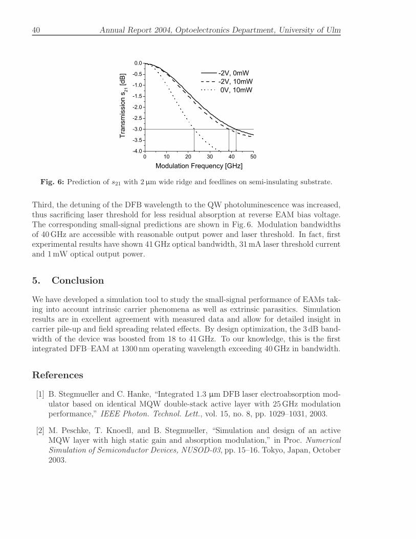
40 Annual Report 2004, Optoelectronics Department, University of Ulm
0 10 20 30 40 50-4.0
-3.5
-3.0
-2.5
-2.0
-1.5
-1.0
-0.5
0.0
Tran
smis
sion
s21
[dB]
Modulation Frequency [GHz]
-2V, 0mW -2V, 10mW 0V, 10mW
Fig. 6: Prediction of s21 with 2 µm wide ridge and feedlines on semi-insulating substrate.
Third, the detuning of the DFB wavelength to the QW photoluminescence was increased,thus sacrificing laser threshold for less residual absorption at reverse EAM bias voltage.The corresponding small-signal predictions are shown in Fig. 6. Modulation bandwidthsof 40GHz are accessible with reasonable output power and laser threshold. In fact, firstexperimental results have shown 41GHz optical bandwidth, 31mA laser threshold currentand 1mW optical output power.
5. Conclusion
We have developed a simulation tool to study the small-signal performance of EAMs tak-ing into account intrinsic carrier phenomena as well as extrinsic parasitics. Simulationresults are in excellent agreement with measured data and allow for detailed insight incarrier pile-up and field spreading related effects. By design optimization, the 3 dB band-width of the device was boosted from 18 to 41GHz. To our knowledge, this is the firstintegrated DFB–EAM at 1300 nm operating wavelength exceeding 40GHz in bandwidth.
References
[1] B. Stegmueller and C. Hanke, “Integrated 1.3 µm DFB laser electroabsorption mod-ulator based on identical MQW double-stack active layer with 25GHz modulationperformance,” IEEE Photon. Technol. Lett., vol. 15, no. 8, pp. 1029–1031, 2003.
[2] M. Peschke, T. Knoedl, and B. Stegmueller, “Simulation and design of an activeMQW layer with high static gain and absorption modulation,” in Proc. NumericalSimulation of Semiconductor Devices, NUSOD-03, pp. 15–16. Tokyo, Japan, October2003.

HVPE of Thick GaN 41
Hydride Vapor Phase Epitaxial Growth of Thick
GaN Layers With Improved Surface Flatness
Peter Bruckner
Thick GaN layers have been grown by hydride vapor phase epitaxy (HVPE) on differentGaN templates grown by metalorganic vapor phase epitaxy. Crack formation could bereduced by using a hydrogen/nitrogen carrier gas mixture. By carefully optimizing thegrowth conditions in the final stage of the process, excellent surface morphologies could beobtained at still acceptably high growth rates. Up to 300 µm thick crack-free HVPE layerswith a mirror like surface could be grown on our FACELO templates.
1. Introduction
Although the recent years have seen a tremendous development of short wavelength opto-electronic and electronic devices based on GaN and related materials, the further improve-ment of such devices is still limited by the fact that epitaxial structures have to be grownon foreign substrates like sapphire, SiC, or Si, because high quality bulk GaN wafers arenot yet really available. Therefore, the heteroepitaxial growth of thick GaN layers byhydride vapor phase epitaxy (HVPE) has been developed in several groups [1] which canbe used as substrates for subsequent device epitaxy. As we have observed on thin GaNlayers grown by metalorganic vapor phase epitaxy, the residual strain depends stronglyon the nucleation method: When an AlN nucleation layer is used, the GaN layer exhibitslarge compressive strain whereas samples with a low temperature GaN nucleation layer- the mostly used method - show much lower strain at room temperature. GaN layersof these types are often used as templates for the deposition of thicker GaN layers byHVPE. Thus, it is interesting to evaluate whether the strain state of these templates mayinfluence the final strain or other properties of the HVPE layers.
Therefore, we have investigated the HVPE growth of thick GaN layers on different GaNtemplates. Besides the cracking behavior, our studies focus also on the surface morphologyproblem and its relation to the template properties. Such studies require an optimizationof all growth parameters to achieve an excellent surface morphology.

42 Annual Report 2004, Optoelectronics Department, University of Ulm
2. Experimental
All HVPE layers have been grown on GaN templates grown on 2-inch-sapphire by MOVPE.This enabled an efficient optimization of the basic growth parameters without the needto optimize the HVPE nucleation process. In order to investigate the influence of thetemplate type and quality, up to 4 different templates could be overgrown simultaneouslyin one HVPE run to get rid of the parameter drift in the reactor. The bare templatesand the overgrown samples with typical layer thicknesses between 40 and 140µm havebeen characterized by standard tools like optical microscopy, high resolution x-ray diffrac-tion (HRXRD), low-temperature photoluminescence (PL) and atomic force microscopy(AFM).
3. Results and Discussion
3.1 Influence of the growth conditions
We have first studied the influence of some basic epitaxial parameters as it is described in[2]. These parameters are the mixture of the carrier gas, the V/III ratio and the reactorpressure. We found that the composition of the carrier gas is of major importance for thegrowth of thick layers, whereas it has only a small influence on the surface morphology.The most important parameters for a change in the surface morphology are the V/III-ratio and the reactor pressure. At higher V/III-ratio more hillocks are visible, but forlower ratios the growth rate decreases. At lower pressures, the surface morphology couldbe improved, whereas higher pressures resulted in larger growth rates due to the reducedgas velocity. Similar trends have peen observed for the V/III-ratio.
These findings led us to the optimization of a 2-step growth procedure: The main part ofour thick GaN layers was growth at those conditions favoring large growth rates, whereasin the very last stage, we reduced pressure and V/III-ratio which resulted in significantlyimproved surface morphologies.
3.2 Influence of the template
As already pointed out, we have done these growth studies on templates, i.e. on thin GaNlayers grown by MOVPE in order to get rid of the difficulty of developing a nucleationprocess in our HVPE system. Several templates were available for these studies which hadbeen grown in different laboratories, but had nominally very similar structures. Standardcharacterization methods also seemed to confirm their equivalence. However, we observedstrong differences of the HVPE grown GaN layers regarding surface morphology andcracking behavior.
As mentioned, low temperature PL and HRXRD measurements showed that the GaNtemplates grown on AlN nucleation layers are strongly compressively strained: We foundthe PL signal of the donor bound exciton (D0, X) typically at 3.492 eV (fig. 1), which

HVPE of Thick GaN 43
corresponds to a relative dilatation of the c lattice constant of ǫ⊥ = ∆ c/c ≈ 1.3 · 10−3
as a consequence of the biaxial compressive strain in the c-plane. This strain is probablymainly due to the thermal mismatch between the GaN layer and the sapphire substrate,indicating that the layer is fairly unstrained at the growth temperature. In contrast,the templates with a GaN nucleation layer show much lower strain of ǫ⊥ ≈ 7 · 10−4,corresponding to a (D0, X) peak position of about 3.482 eV (fig. 1).
Besides the different nucleation, the templates were grown identically. Indeed, the HVPElayers grown on these two types of templates show very similar surface morphology. Asmeasured by PL, the strain difference is still seen after epitaxy, although both layers arenow fairly unstrained with the (D0, X) peak being close to 3.471 eV (fig. 1 b). How-ever, the tendency to form cracks, if not grown under perfect conditions, is much morepronounced for the template U1 (GaN nucleation) whereas template U2 is still free ofcracks. This may be a consequence of the strain-free situation at growth temperature,whereas the layers on the GaN nucleation are obviously strained tensely at these hightemperatures and thus may form cracks during cool down.
a)3.46 3.48 3.50 3.52 3.54
0.1
1
10
100
1000
T. U1 (GaN nucleation) T. U2 (AlN nucleation)
PL energy (eV) b)3.45 3.46 3.47 3.48 3.49 3.50 3.51 3.52
0.1
1
10
100
1000
0.1
1
10
100
1000
Inte
nsity
(a.
u.)
on U1 (GaN nucleation) on U2 (AlN nucleation)
PL energy (eV)
Fig. 1: PL spectra (T = 15 K) of the bare templates (a) and 40 µm thick HVPE layers grownon them (b).
3.3 Growth on a FACELO-template
When we apply the optimized HVPE process on our FACELO-templates, we were ableto increase the final thickness before cracking significantly. The FACELO-process itself isdescribed more precisely in [3].
Even if we start with a fairly rough surface (fig. 2 (a)) more than 130µm thick HVPE layers(fig. 2 (b)) with improved surface morphology and better crystalline quality compared tothe FACELO-template could be grown. On the FACELO-templates, a typical wing-tiltof 0,5 was observed, whereas no wing-tilt was measurable after the HVPE growth.
Finally, we were able to grow up to 300µm GaN directly on such a FACELO-template.For the evaluation of these layer, we have to take care about the wafer curvature, which

44 Annual Report 2004, Optoelectronics Department, University of Ulm
is mainly caused by the different thermal expansion coefficients between sapphire andGaN during cool down. Because of the non circular symmetry of our stripe-mask forthe FACELO-template, two different bowing radius developed with 75 cm parallel to thestripes and 40 cm perpendicular to them. In spite of the strong curvature these layers arestable and crack free.
a) b)
Fig. 2: Optical Nomarski interference micrograph of the surface of a 130 µm HVPE layer (b)grown on a lower quality FACELO-template (a)
4. Summary
By optimizing the growth parameters of our HVPE process, we could significantly improvethe quality of thick GaN layers. The tendency to form cracks could be further reducedby applying compressively strained GaN templates grown on an AlN nucleation layer.We could demonstrate that a thorough optimization at the end of the growth-processcould significantly improve the surface morphology. Therefore we were able to grow upto 300µm GaN crack-free on a FACELO-template.
References
[1] X. Xu, R.P. Vaudo, C. Loria, A. Salant, G.R. Brandes, and J. Chaudhuri, “Growthand characterization of low defect GaN by hydride vapor phase epitay,” J. CrystalGrowth, vol. 1-3, no. 246, p. 223, 2002.
[2] F. Habel, “Investigations of the Carrier Gas Composition for HVPE of GaN,” AnnualReport 2003, Optoelectronics Department, University of Ulm, pp. 77–80, 2003.
[3] F. Habel, “Optimization of GaN FACELO Structures using Marker Layers,” AnnualReport 2004, Optoelectronics Department, University of Ulm, 2004.
GaN FACELO Structures With Marker Layers 45
Optimization of GaN FACELO Structures
Using Marker Layers
Frank Habel
The FACELO technique was used to further reduce the dislocation density of GaN layers.AlGaN and Si-doped GaN layers were implemented as marker layers during GaN epitaxialgrowth in order to get a deeper scientific understanding of the growth process. Both typesof marker layers show a good visibility without any parasitic influences on the crystalstructure or growth behavior. These marker layers were used to study the development ofthe different crystal facets as growth proceeds. This technique provided access to a precisecontrol of a multistep growth sequence, enabling a thorough optimization of our FACELOprocess by inserting additional properly designed growth steps.
1. Introduction
Due to the rapid progress in the development of high-end GaN based devices such as laserdiodes, ultra violet light emitting diodes and field effect transistors, the role of threadingdislocations is getting more and more important. The dislocation density in commonheteroepitaxially grown GaN on sapphire or silicon carbide substrates is in the order of108-1010 cm−2, due to the lattice mismatch between these substrates and GaN togetherwith the resulting columnar structure of the grown layers. Dislocations have several strongeffects on devices. Especially for laser diodes, a low dislocation density is a prerequisite forlong device lifetimes. Moreover, dislocations act as non-radiative recombination centers[1], reducing the efficiency of optoelectronic devices especially in the violet and UV range[2]. Carrier mobility is affected by scattering at charged dislocation lines. The formationof V-defects during growth of InGaN quantum wells is correlated with dislocations [3].One of the most promising techniques to reduce the dislocation density is the growthon structured substrates. The basic method is epitaxial lateral overgrowth (ELOG) [4],which benefits from the fact, that dislocations usually run vertically from the substrateinterface right to the surface of the semiconductor layer, whereas laterally grown crystalareas are nearly dislocation free. An advanced method is the facet assisted epitaxiallateral overgrowth (FACELO), where the propagation of the dislocations is affected byappropriate control of the dominating crystal facets during growth. This method requiresa fairly complex variation of the epitaxial parameters during growth to enable optimizedvertical and lateral growth at different times of the process. However, from the final layerproperties, it is very difficult to judge the success of some optimization procedure of anintermediate growth step. This problem can be overcome by the use of marker layers

46 Annual Report 2004, Optoelectronics Department, University of Ulm
Step 2
Step 1
Fig. 1: Schematic drawing of a FACELO structure (left) and corresponding TEM image (right)showing the bending of the threading dislocations.
which make visible how the growth proceeds [5]. Therefore, we have studied AlGaNand Si doped marker layers in order to optimize our FACELO process by implementingadditional, specially designed growth steps.
2. FACELO
The FACELO process is a further development of the ELO technique. Therefore, thesamples have to be prepared in the same way. For the structured substrates 1µm thickGaN layers on sapphire were used as templates. They were covered with a 250 nm thickSiO2 mask deposited by PECVD. By standard lithography and dry etching in a CF4 RIEsystem 3–8µm wide stripes have been opened. The structured growth was performed bymetalorganic vapor phase epitaxy in an Aixtron 200/4 RFS horizontal reactor system.The basic investigations of structured growth have already been published [5]. For theFACELO process at least two growth steps are required as it is shown in figure 1a. Inthe first step, a triangular shaped cross section is formed, confined by 1122 facets.This structure is achieved using a low growth temperature of about 1020C. In the nextstep the temperature is raised and the growth parameters are adjusted to obtain a highlateral growth rate. This change form vertical to lateral growth leads to a change ofthe propagation direction of the threading dislocations. The dislocations are bent at theinterface of the triangular structure and continue horizontally, the material above thisstructure is completely dislocation free (fig. 1b).
In figure 2 the distribution of dislocations of FACELO samples is shown. For 8µm widemask openings the triangular structure was not completed yet, so a stripe with a highdislocation density is still found. In contrast, above the 4µm wide mask openings almostno dislocations were found, the dislocation density in this are is in the range of 106cm−2.This excellent value demonstrates the successful realization of the FACELO process.
Unfortunately, these samples showed a macroscopically rough surface morphology. Thischallenge can be overcome by implementing additional growth steps to level the surface.

GaN FACELO Structures With Marker Layers 47
Fig. 2: Distribution of dislocations of FACELO samples depending on the mask opening deter-mined using an HCl etching technique. Mask opening is marked by black bar.
In order to optimize and control several growth steps, it is necessary to have a method toanalyze every single step. Therefore we implemented the marker layer technique.
3. Marker Layers
During epitaxial growth TMAl or silane was periodically added to the reactor for 1.5minutes in order to form a periodic pattern of AlGaN or Si-doped GaN, respectively. Theresulting thickness of these marker layers was between 50 and 200 nm , depending on thedifferent growth rates for different crystal facets and growth parameters. After growththe cross sections of the samples were analyzed using a scanning electron microscope.The AlGaN layers could be detected for an aluminium content of 3% and were clearlyvisible for an aluminium content of 10%. Similarly, the n-doped layers were alreadyvisible for a silicon concentration of 1×1019cm−3 and showed a good visibility for a highersilicon concentration of 5×1019cm−3 (figure 3a). The given numbers are nominal valuescorresponding to growth of plane layers in c-direction, as the exact concentration valuesmay be different for growth in different crystal directions and depend also on the maskstructure.
These concentrations obviously did not affect the normal GaN growth process, as hasbeen checked additionally by cathodoluminescence (CL, performed by T. Riemann and

48 Annual Report 2004, Optoelectronics Department, University of Ulm
(a) (b)
Fig. 3: GaN:Si marker layers make the propagation of the facets visible (a). Increased growthrate at coalescence region (b).
J. Christen, Otto-von-Guericke University Magdeburg): The marker layers could also bedetected, but for both types neither a decrease in CL intensity nor a strain induced shiftof the CL wavelength was found in the GaN material between the marker layers. Thesurface morphology was investigated using an optical microscope. Again no difference inmorphology was found between samples grown with and without marker layers. Never-theless, we did not study higher concentrations in order not to introduce any parasiticgrowth effects.
In cross sectional SEM scans of the samples, each marker layer directly indicates theposition and shape of the growing facet for the respective point in time. As the growth timebetween two marker layers is known and the thickness of the deposited material can easilybe measured, the growth rates can be calculated. If several growth steps with differentparameters are used, this method provides direct access to the growth rates for each crystaldirection and each set of parameters in only one growth run. Therefore the number ofgrowth experiments can be drastically reduced, which otherwise would be necessary tostudy the influence of different growth parameters on the local growth rate. This techniquealso allows deeper insight in several growth details. For example, an increase of the growthrate was observed at the coalescence region (fig. 3b). Moreover, the development of someunwanted growth features could be monitored. We could unambiguously observe thatthe propagation of inverse pyramidal shaped growth defects originate already from thetemplate surface. The full potential of the marker layer technique becomes evident whenepitaxial growth consisting of several different growth steps is developed.
3.1 Multi-Step Growth
Obviously, an improvement of these FACELO structures is possible when a growth se-quence consisting of even more steps is used. For example, the low temperature growth

GaN FACELO Structures With Marker Layers 49
23
4
1
Fig. 4: SEM scan and schematic of a multi step FACELO sample.
step used for the triangular structures may cause growth defects when carried out asfirst step directly on the structured template. As the crystal quality decreases when thegrowth rate becomes too high, a reduced growth rate during coalescence leads to im-proved results. After coalescence another set of growth parameters may be used to getan improved surface morphology. On the other hand, the control of the growth sequencegets more difficult when the number of growth steps is increased. The accurate timing ofa multi step growth sequence is much more sensitive. Although the basic effects of themain growth parameters like temperature, pressure and V-III ratio on growth in differentcrystal directions are fairly well known [4], these data are not precise enough to describethe exact behavior of the propagating facets when the main parameters are changed dur-ing growth. In order to develop a multi step growth sequence using conventional tools,a tremendous number of experiments is necessary, as each step has to be optimized in aseparate series of growth runs. The marker layer technique allows the optimization of allgrowth steps simultaneously in a few experiments, as a correlation between the differentgrowth steps and the grown facets is possible for every point in time. Based on thattechnique we further improved our FACELO structure. In figure 4 a SEM scan and thecorresponding schematic of the cross section of such a multi step FACELO sample aredepicted. Due to the marker layers, all growth steps are clearly visible. At first, growth isinitiated with standard GaN parameters (high temperature, standard pressure, standardV-III ratio). Then the triangular section is formed using a decreased growth temperature.In the next step, the lateral overgrowth is favored by lowering the reactor pressure andincreasing the V-III ratio. In the final growth step, the temperature is raised again aftercoalescence in order to level the surface and to improve the morphology. Every single stephas been individually optimized in a few preceding experiments. As can be easily seen,the triangular structure has been completed up to the tip, so the FACELO technique wascarried out completely. Therefore the marker layer method enabled us to develop a multistep growth sequence to grow complete 2 inch wafers with low dislocation density andexcellent surface morphology (figure 5).

50 Annual Report 2004, Optoelectronics Department, University of Ulm
Fig. 5: Excellent surface morphology of a multi step FACELO sample.
4. Conclusion
GaN:Si and AlGaN layers were implemented as marker layers for the epitaxial growthof GaN on structured substrates. For a silicon concentrations of 5 × 1019cm−3 or analuminium content of 10%, the marker layers are well visible in SEM scans. On the otherhand, no parasitic side effects on the crystal quality or surface morphology were found.The marker layers provide direct access to the propagating growth facets in differentcrystal directions and under different growth conditions. Therefore, this technique is anoutstanding tool for the development of multistep growth sequences thus enabling usto grow low dislocation density GaN with excellent surface morphology on full 2 inchstructured substrates.
References
[1] D. Cherns, S.J. Henley, and F.A. Ponce, “Edge and screw dislocations as nonradiativecenters in InGaN/GaN quantum well luminescence,” Appl. Phys. Lett., vol. 78, no. 18,pp. 2691–2693, 2001.
[2] T. Stephan, M. Kunzer, P. Schlotter, W. Pletschen, H. Obloh, S. Muller, K. Kohler,and J. Wagner, “Importance of Nonradiative Recombination Processes in Violet/UVInGaN Light Emitting Diodes,” phys. stat. sol. (a), vol. 194, no. 2, pp. 568–571,2002.
[3] J.S. Speck and S.J. Rosner, “The role of threading dislocations in the physical prop-erties of GaN and its alloys,” Physica B, vol. 273–274, pp. 24–32, 1999.
[4] B. Beaumont, Ph. Vennegues, and P. Gibart, “Epitaxial Lateral Overgrowth of GaN,”phys. stat. sol. (b), vol. 227, no. 1, pp. 1–43, 2001.
[5] F. Habel, “Dislocation Reduction by GaN MOVPE Growth on Structured Sub-strates,” in Annual Report, Optoelectronics Department, University of Ulm, pp. 3–6,2002.

Epitaxial Growth of AlGaN Layers 51
Epitaxial Growth of High Al-Containing AlGaN and
AlN Layers With MOVPE
Christoph Kirchner
We report on the epitaxial growth of AlN- and high aluminum containing AlGaN-layerswith MOVPE. The growth process of such layers is much more crucial than for GaNgrowth. The difficulties like achieving a good material quality, undesired prereactions inthe gas phase and low growth rates are discussed. Layers of AlxGa1−xN with Al-contentsx up to 80% and pure AlN have been succesfully grown. First results of epitaxial layercharacterization are presented.
1. Introduction
High aluminum containing AlGaN an AlN layers are of increasing interest for the III-V nitride device technology. Important applications are e.g. UV-LEDs and solar blindUV-detectors [1], [2]. Such devices have a broad application range on the field of sensorsand spectroscopy, e.g. environmental analytics, UV-desinfection of water or as excitationsource for photochemical reactions (hardening of polymers). For emission wavelengthsbelow 365 nm it is mandatory to use AlGaN layers in the active regions as recombinationareas. Depending on the desired wavelenght, Al-contents up to 50% are necessary (UV-LEDs with λp =270 nm emission wavelength). Due to enhanced absorption in the p-typeGaN layers for wavelenghts below 350 nm, the outcoupling of light must be realized troughthe transparent sapphire substrate. This means, that all layers between the active regionand the substrate must be transparent, too. Therefore, the Al-contents in these layersmust be higher than in the active layers, in extreme cases pure AlN is mandatory. Anotherinteresting field of applications are AlN/GaN quantum cascade lasers, which are usingintersubband transitions for near-, mid- and far infrared emission [3]. Fabrication of suchdevice structures becomes more and more critical with decreasing wavelenghts, becausecrystalline and optical quality of nitride layers decreases with increasing Al-contents [4].
One major problem during epitaxy of AlN and AlGaN with high Al-content by MOVPEis the strong reactivity of the metalorganic aluminum source TMAl (trimethylaluminum):parasitic reactions between ammonia and TMAl result in depletion of the gas phase lead-ing to a strongly reduced growth rate. In extreme cases, formation of small AlN crystallitesin the gas phase occur, which are falling on the substrates and strongly influence the layerquality. Our experiments show that the prereactions can be reduced by appropriate choiceof the growth parameters, but not completely avoided. A very important parameter isthe reactor pressure, which has to be strongly reduced for AlN growth. In spite of thisparameter optimization, growth rate remains quite small.

52 Annual Report 2004, Optoelectronics Department, University of Ulm
2. Experimental
Epitaxial growth of high Al-containing compound AlGaN and AlN semiconductor filmsis conducted in a single wafer, radio-frequency heated, horizontal type, water cooledquartz reactor MOVPE system (Aixtron AIX 200 RF) operated at low pressure. TheMOVPE system is equipped with a reflectometer system consisting of a white light sourceand a CCD spectrometer. This measurement system allows in situ reflectometry duringepitaxial growth for determining growth rates and surface development, which is a helpfultool for process development. Trimethylgallium (TMGa), trimethylaluminum (TMAl)and ammonia (NH3) are used as group III and group V precursors, respectively. Allgrowth experiments are performed on c-plane sapphire (Al2O3), using a low temperaturenucleation layer process before the main layer growth.
2.1 Epitaxial growth of AlGaN
A low pressure epitaxy process allows successful growth of AlGaN with Al-contents upto 80%. Fig. 1 shows Al-incorporation in the solid (determined by high resolution x-raydiffraction (HRXRD)) vs. the molar TMAl/TMGa ratio at a pressure of 50mbar. Molarflows of TMGa and TMAl were varied in a range of 3.5 - 45µmol/min and 25 - 90µmol/min,respectively. As can be seen, a very high Al/Ga ratio in the gas phase is necessary even atsuch low pressures to achieve a high aluminum content in the solid. Problems arise fromthe high reactivity of TMAl: Only low growth pressures allow significant Al-incorporation.Pressures, which are usually used for the growth of GaN (150 - 200mbar), result in nearlyzero growth rate. Pressures above 300mbar result in spontaneous formation of smallAlN crystallites in the gas phase, which are falling on the substrates, destroying thelayer surface. The crystal quality of the low-pressure grown AlGaN-layers is quite good,which can be seen from fig. 2, where a 2Θ -ω HRXRD scan is plotted. The measuredstructure consists of a 1µm thick undoped GaN layer, grown on sapphire with a lowtemperature GaN nucleation layer, and a 100 nm thick Al0.8Ga0.2N layer. The peaks fromthe underlying GaN-layer and the AlGaN peak can be clearly resolved. FWHM is 230arcsec for the GaN layer and 350 arcsec for the AlGaN-layer, respectively.
2.2 Epitaxial growth of AlN
The above mentioned problems are even more significant for the growth of pure AlN.Epitaxial growth of AlN shows a very low growth rate. Enhanced prereactions in thereactor are depleting the gas phase before reaching the substrate. Only at pressures of50mbar and below, significant growth rates are observed. At 25mbar, a fairly large growthrate of 550 nm/hr could be achieved. With even lower reactor pressures a higher growthrate might be reached, but the minimum reactor pressure is limited by the pumpingsystem. In fig. 3, the AlN growth rate is plotted against the reactor pressure, while theother parameters are kept konstant. All AlN-layers are grown with a low temperature

Epitaxial Growth of AlGaN Layers 53
0,3 0,4 0,5 0,6 0,7 0,8 0,9 1,00
10
20
30
40
50
60
70
80
90
Al-co
nte
nt[%
]
molar ratio Al/(Al+Ga)
Fig. 1: Al-content in AlxGa1−xN vs. molarTMAl/TMGa-ratio at a reactor pressure of50 mbar.
17,0 17,5 18,0 18,5 19,0 19,5
100
1000
100002q-wscan
100 nmAl
0,8Ga
0,2N
GaN
inte
nsi
ty[a
.u.]
w
Fig. 2: HRXRD-scan (2Θ -ω) of 100 nmthick Al0.8Ga0.2N, grown on GaN.
AlN-nucleation layer. The analysis of the AlN layers with HRXRD reveals a quite goodcrystal quality, as can be seen from fig. 4, where a rocking curve of undoped AlN is shown.
20 30 40 50 60 70 80
100
200
300
400
500
600
gro
wth
rate
[nm
/hr)
pressure [mbar]
Fig. 3: MOVPE growth rate of epitaxialAlN plotted versus reactor pressure.
17,6 17,8 18,0 18,2 18,4 18,6
0
500
1000
1500
2000
2500
3000
3500in
tensi
ty[a
.u.]
w
Fig. 4: Rocking curve (0002-reflex) of500 nm AlN, grown on sapphire. FWHM is600 arcsec. Peak position is at 18.06.
For examination of the spectroscopic quality, low temperature cathodoluminescence (CL)-measurements were performed. In fig. 5, the CL-spectrum of the 500 nm thick AlN-layeris displayed. The near-bandedge transition at 6.017 eV is clearly resolved with a FWHMof 30meV. The logarithmic insert makes the LO-phonon replica visible, which indicate ahigh optical quality of the AlN-layer.
3. Conclusion
We presented epitaxial growth of AlGaN and AlN layers with MOVPE. Implementation ofa low pressure growth process allows fabrication of layers with good optical and crystalline

54 Annual Report 2004, Optoelectronics Department, University of Ulm
AlN / Sapphire
T=5K
5.7 5.8 6.1
215
0
5
10
15
20
25
30210 205
6.05.9
Vacuum wavelenght [nm]
Energy [eV]
Inte
nsity [a.u
.]
XA
6.017eV
(D0X)?
XA
-2 LO
-LO
Energy [eV]
Vacuum wavelength [nm]
5.8 6.16.05.9
10
100
215 210 205
Inte
nsity [
a.u
.] T=30K
Fig. 5: Low temperature CL-spectra of a 500 nm thick undopedAlN layer, grown on sapphire. Theneutral donor bound exciton D0Xand a free exciton (XA) can beresolved. The insert in logarith-mic scale shows the LO-phononreplica, indicating high optical ma-terial quality (Measurements per-formed by G. Prinz, Dept. of Semi-conductor Physics, Univ. Ulm).
quality. The prereactions in the gas phase can be sufficiently suppressed but not com-pletely avoided, resulting in reduced growth rates. Our experiments show, that epitaxialgrowth of AlN and AlxGa1−xN with high Al-fractions x up to 80% can be succesfullyperformed with our MOVPE system.
References
[1] H. Sun, V. Adivarahan, S. Wu, J.P. Zhang, A. Chitnis, M. Shatalov, V. Mandavilli,J.W. Wang and M. Asif Khan, “AlGaN-based 280 nm light-emitting diodes withcontinuous wave powers in excess of 1.5 mW”, Appl. Phys. Lett., vol. 85, p. 531,2004.
[2] Y. Jung, J. Lee, J. Kim, Y. Lee, M.-B. Lee, J.-H. Lee and S. Hahm “Pt/AlGaNMetal Semiconductor Ultra-Violet Photodiodes on Crack-Free AlGaN Layers” Jpn.J. Appl. Phys., vol. 42, p. 2349, 2003.
[3] Y. Inoue, H. Nagasawa, N. Sone, K. Ishino, A. Ishida, H. Fujiyasu, J.J. Kim,H. Makino, T. Yao, S. Sakakibara and K. Kuwabara, “Fabrication and characteriza-tion of short period AlN/GaN quantum cascade laser structures”, J. Crystal Growth,vol. 265, p. 65, 2004.
[4] N. Nakada, H. Ishikawa, T. Egawa and T. Jimbo, “Suppression of Crack Genera-tion in GaN/AlGaN Distributed Bragg Reflector on Sapphire by the Insertion ofGaN/AlGaN Superlattice Grown by Metal-Organic Chemical Vapor Deposition”,Jpn. J. Appl. Phys., vol. 42, p. L144, 2003.

InGaN QWs Grown on Facets 55
Electroluminescence From GaInN Quantum Wells
Grown on Non-(0001) Facets of Selectively Grown
GaN Stripes
Barbara Neubert and Peter Bruckner
Non-(0001) GaInN QWs have been grown by low pressure MOVPE on side facets oftriangular shaped selectively grown GaN stripes. By analysing low temperature photolu-minescence and room temperature electroluminescence, we found strong indications, thatboth, In and Mg are less efficiently incorporated on these side facets compared to the com-mon (0001) plane with even lower efficiency for stripes running along 〈1100 〉 comparedto 〈1120〉. Nevertheless, we observed strong light emission from these quantum wells,supposed to be at least partly caused by the reduced piezo-electric field.
1. Introduction
The group III nitrides play an important role for light emitting devices, because theirspectra reach from UV to visible wavelengths. High brightness LEDs and laser diodes havebeen fabricated. Due to their strong polarity, group III nitrides show large piezoelectricconstants along the 〈0001〉 axis. Therefore strong piezoelectric fields (PFs) are induced inbiaxially strained GaInN quantum wells (QWs) grown on such 〈0001〉-oriented GaN. Thisgives rise to a spatial separation of the electron and hole wave functions what hamperstheir radiative recombination. A higher probability for radiative recombination can beexpected for QWs grown along directions other than the most commonly used 〈0001〉[1], thus potentially leading to improved optical characteristics for light emitting devices.To this end, some groups have investigated the growth of a-plane structures on r-planesapphire. However, up to now only lower quality layers with a large dislocation densitycould be grown [2]. Therefore, we have grown GaInN QWs on non-(0001) facets ofselectively deposited GaN stripes with triangular cross-section, where we expect reducedPFs with still low defect densities, in order to evaluate their geometry and facet dependentoptoelectronic properties.
2. Experiment
The samples under study have been grown by low pressure metal organic vapor phase epi-taxy (MOVPE) in a conventional horizontal reactor. A 1.5µm thick GaN template wasgrown first on c-plane sapphire, then was covered with a 200 nm SiO2 mask by plasma

56 Annual Report 2004, Optoelectronics Department, University of Ulm
enhanced chemical vapor deposition (PECVD) and structured by conventional opticallithography and reactive ion etching (RIE) to serve as regrowth mask. We patternedthe SiO2 with two stripe directions perpendicular to each other. The dimensions of themask openings and mask periods ranged from 4 to 8µm and from 6 to 300µm, respec-tively. We generated silicon doped GaN stripes with triangular shape having 1122-facetsfor 〈1100〉-orientation and 1101-facets for 〈1120〉-orientation. Stripes between narrowmasks developed a trapeze-like cross-section due to their locally lower growth rate. Onthese n-doped GaN stripes we have grown a period of 5 nominally 3 nm thick GaInNQWs, containing about 10% In, separated by 10 nm thick GaN barriers followed by ap-doped GaN top layer. For comparison, the same structure was grown without any Siand Mg doping. These samples have been characterized by scanning electron microscopy(SEM), photoluminescence (PL), cathodoluminescence (CL) both at low temeperatureand electroluminescence (EL) at room temperature (RT).
3. Results and Discussion
SEM cross-section micrographs showed that the QWs were grown on the side facets ofour stripes as well as on the top facet of the trapeze-like stripes. We found that theformer were typically 2 to 3 times thinner than the top QWs, obviously due to stronginterfacet material migration, first transmission electron microscopy studies confirmedthese findings.
The dependence of the PL signal at 20K on the mask stripe width of the undoped sampleis shown in fig. 1. We observed a red shift of the PL maximum for increasing mask widthat fixed opening of 6µm. Similar results have been obtained by CL spectra taken overthese different stripes. This shift is probably due to the locally increasing growth rateas a consequence of the increasing mask area [3], further enforced by the more efficientIn incorporation with increasing growth rate [4]. Obviously, more In is incorporated intothe QWs on the stripes running along the 〈1120〉 direction. For trapeze shaped stripes in〈1100〉 direction, we find a second maximum of lower intensity at longer wavelengths (fig.2).
We attribute the short wavelength emission to the GaInN QWs on 1122-facets while theweaker emission at longer wavelengths stems from the GaInN (0001) top QWs. Compara-ble results have been obtained by Nishizuka et. al. [5] by PL microscopy. Due to the largewavelength difference observed in our samples, we think that this shift can only partly beattributed to the different PFs in these QWs, whereas their different thickness mentionedabove and changed In incorporation may be also important factors. Even compared tounstructured (0001) reference QWs which emit at 421 nm, the signal of the top QWs isshifted to longer wavelengths confirming increased In incorporation. Probably, interfacetdiffusion of In from the side facets to the top facet plays a major role.
For first electroluminescence (EL) experiments we deposited In and Ni/Au test structureson top of the stripes by e-beam evaporation after activation of Mg at 800C for 10min innitrogen ambient. The Ni/Au metallisation was annealed at 400C for 10min in nitrogen

InGaN QWs Grown on Facets 57
0 2 4 6 8 10 12 14 16 18 20 22370
380
390
400
410
420
1-100, opening 6 µm 11-20, opening 6 µm
PL p
eak
emis
sion
[nm
]
SiO2 stripe width [mm]
Fig. 1: PL peak positions for stripes along〈1100〉 and 〈1120〉.
400 450 500 5500.1
1
10
100
1000
trapeze, 4µm SiO2, opening 6mm, (1-100) triangular, 12µm SiO2, opening 6mm, (1-100)
PL in
tens
ity @
20K
[arb
.u.]
wavelength [nm]
Fig. 2: PL signal for trapeze (solid line) andtriangular shaped stripes (interrupted line).
ambient. Due to the large area of our p-type contacts, several stripes were excited simul-taneously inhibiting EL studies on single stripes. Even with this simple contact geometry,we measured fairly large light output powers of nearly 1mW at 20mA (figure 3). Thefairly high resistivities of these structures may be explained by lower Mg incorporationefficiency into the side facets compared to the (0001) layers [6]. Similar as in PL, trapezestripes in 〈1100〉 direction show two maxima (fig. 4). The higher intensity of the longerwavelength peak may support the hypothesis that the Mg incorporation is reduced on theside facets emitting at shorter wavelength. However, strong spectra obtained on pure tri-angular facets (fig. 4 dotted line) demonstrate that also on these side facets pn junctionshave been formed.
4. Conclusion
Our studies show that LED structures can be grown on side facets of selectively grownstripes with triangular cross-section. The observed strong light emission of GaInN QWs onthese facets may be partly a consequence of the reduced piezo-electric field in these layers.By analysing different luminescence experiments, we conclude that the In incorporationefficiency depends on the stripe direction and is lower on these side facets as compared tothe (0001) plane. We found some indications that the Mg incorporation follows similartrends.
Acknowledgments
We like to thank J. Christen and T. Riemann of Otto-von-Guericke-University in Magde-burg and M. Schirra of University Ulm for CL measurements and M. Beer and J. Zweck

58 Annual Report 2004, Optoelectronics Department, University of Ulm
0 10 20 30 40 500.0
0.5
1.0
1.5
2.0
ou
tput
pow
er P
opt. [m
W]
current I [mA]
Fig. 3: EL intensity of stripes in 〈1120〉 direc-tion.
350 400 450 500 550
-20
0
20
40
60
80
100
120
trapeze, 4µm SiO2, opening 6mm, (1-100) triangular, 10µm SiO2, opening 6mm, (1-100)
EL in
tens
ity [a
rb.u
.]
wavelength [nm]
Fig. 4: EL spectra of trapeze (solid line) andtriangular (dotted line) shaped stripes.
of University in Regensburg for TEM measurements.
References
[1] T. Takeuchi, S. Lester, D. Basile, G. Girolami, R. Twist, F. Mertz, M. Wong, R.Schneider, H. Amano, and I. Akasaki, “Polarization control in nitride-based semi-conductor,” in Proc. Int. Workshop of Nitride Semiconductors IPAP Conf. I., Tokyo,Japan, pp. 137–140, September 2000.
[2] M.D. Craven, S.H. Lim, F. Wu, J.S. Speck, , and S.P. DenBaars, “Structural charac-terization of nonpolar (1120) a-plane GaN thin films grown on (1102) r-plane,” Appl.Phys. Lett., vol. 81, no. 3, pp. 469–471, 2002.
[3] Y.D. Galeuchet, P. Roentgen, and V. Graf, “GaInAs/InP selective area metalorganicvapor phase epitaxy for one-step-grown buried low-dimensional structures,” J. Appl.Phys., vol. 68, no. 2, pp. 560–568, 1990.
[4] S. Keller, B.P. Keller, D. Kapolnek, A.C. Abare, H. Masui, L.A. Coldren, U.K. Mishra,and S.P. DenBaars, “Growth and characterization of bulk InGaN films and quantumwells,” Appl. Phys. Lett., vol. 68, no. 22, pp. 3147–3149, 1996.
[5] K. Nishizukaand M. Funato, Y. Kawakami, Sg. Fujita, Y. Narukawa, and T. Mukai,“Efficient radiative recombination from 〈1122〉-oriented InxGa1−xN multiple quan-tum wells fabricated by the regrowth technique,” Appl. Phys. Lett., vol. 85, no. 15,pp. 3122–3124, 2004.
[6] T. Akasaka, S. Ando, T. Saitoh, and N. Kobayashi, “Current-confining structure ofInGaN hexagonal microfacet lasers by selective incorporation of Mg during selective-area MOVPE,” J. Crystal Growth, vol. 248, pp. 537–541, 2003.

Longitudinal Mode Patterns in GaInN Lasers 59
Observation of Longitudinal Mode Patterns in
Violet-Blue GaInN-Based Laser Diodes
Christoph Eichler and Daniel Hofstetter
We report on temperature-independent longitudinal mode patterns in GaInN-based violetdiode lasers. The lasers were operated at cw lasing threshold; and the emission spec-tra were analyzed at a range of temperatures using a high resolution Fourier transformspectrometer. The envelopes of the longitudinal modes showed a characteristic irregularpattern which tuned with temperature at the same rate as the modes themselves. A sim-ulation of the longitudinal modes supports the idea that we see the signature of quantumwell thickness fluctuations or indium clusters.
1. Introduction
Optoelectronic devices based on nitride semiconductors have seen a decade of rapidprogress which culminated in the successful commercialization of visible light-emittingdiodes (LEDs) and violet-blue laser diodes (LDs). Despite of this success, the nitridesare still a material system with many unknown material parameters. This is in particulartrue for the ternary compound GaInN which plays an important role in state-of-the-artoptoelectronic devices [1]. Its considerable lattice mismatch with respect to GaN hasobvious consequences like strain or piezo-electric polarization. Other problems arise fromthe thermodynamic immiscibility of GaN and InN over a wide range of compositions andtemperatures [2] leading to problems such as segregation during growth and carrier local-ization in a nominally two-dimensional electronic system [3]. Especially with respect tothe last two points, there has been considerable effort to clarify the role of quantum-dotlike carrier confinement for the efficiency of visible light emission.
Using photoluminescence (PL) and various transmission electron microscopy (TEM) ap-proaches, several researchers found strong carrier localization due to In-rich clusters withinGaInN quantum wells. The size of the clusters is typically about 3 nm, with an In contentreaching values of 60–80% [4, 5, 6]. Although electron beam treatment produces inho-mogeneous strain which might result in an over-estimation of the In clustering [7], thereappears clear evidence for such a clustering mechanism. On the other hand, thickness fluc-tuations of the quantum wells can provide significant carrier localization too, supposedlyleading to improved efficiency [8].
In this article, we present spectral investigations on GaInN laser diodes which may shedlight on this open question from a quite unusual approach. When the lasers are driven

60 Annual Report 2004, Optoelectronics Department, University of Ulm
continuously slightly above threshold, they show a specific longitudinal mode pattern,which shifts at the same temperature rate as the longitudinal modes themselves. Althoughdifferent explanations are possible, we strongly believe that this spectral modulation isthe result of carrier localization due to In clustering and/or well thickness fluctuations.
2. Experimental
We investigated a commercial laser diode from Nichia, Inc. grown on sapphire and a devicefabricated at OSRAM Opto Semiconductors grown on SiC. The latter device structure isdescribed elsewhere [9]. During the experiment, spectral measurements were carried out atdifferent cw currents and at a range of different temperatures. Special attention was paidto the operating point which remained close to the cw threshold for all temperatures. Theoutput of the laser diode was collimated to a parallel beam and coupled into a Nicolet870 Fourier transform spectrometer. Measurements were carried out at the maximumresolution of 0.1 cm−1, averaged over 100 single scans, and detected using the internalSi-photodiode.
3. Experimental Results and Discussion
Under these conditions, two sets of longitudinal modes could be resolved which belongto two different lateral mode families (inset of fig. 1). In order to highlight the relevantinformation, all other spectra contain the maxima of each longitudinal mode only, thusrepresenting the envelope of each spectrum (fig. 2). As seen in fig. 1, currents well belowthreshold imply a smooth spectral envelope without modulation. Increasing the currentleads to an almost linear blue shift of the peak emission wavelength due to band fillingwhile maintaining the smooth shape of the envelope. As the current approaches lasingthreshold, the carrier density gets pinned and thus the peak wavelength rests at a nearlyconstant value. At the same time, the spectral envelope starts to show some modulationfeatures. As shown schematically in fig. 3 (top), we believe that this ripple is due toIn composition or well width fluctuations, which again result in a modulation of thequantum well depth. In those well regions with an energetically deep ’hole’, carriers getlocalized, thus leading to a modulation of the carrier density across the well. For lowcurrents, carriers in ALL areas will contribute to spontaneous emission and nonradiativerecombination, i.e. the modulation just broadens the emission spectrum. As the currentgets closer to lasing threshold, the carrier density in the deep areas of the well becomessufficiently high to produce gain. Different longitudinal modes then benefit differentlyfrom each such gain center, as depicted in fig. 3. At position ”1”, mode m has a node andthus does not see any amplification at this point within the resonator. But mode m+1 hasa maximum at position ”1”, so it benefits fully of the amplification at this point. Likewise,at position ”2” mode m + 1 has a node and sees no amplification, whereas mode m stillis amplified. At position ”3” finally, both modes see the same amplification. Added up

Longitudinal Mode Patterns in GaInN Lasers 61
4 0 6 4 0 7 4 0 8 4 0 9 4 1 01 0 0
1 0 1
1 0 2
1 0 3
1 0 4
1 0 5
1 0 5 m A1 0 1 m A1 0 0 m A
9 0 m A
5 0 m A7 0 m A
O s r a m 1 3 ° C l p e a k
Enve
lope (
a.u.)
W a v e l e n g t h ( n m )
4 0 7 . 1 0 4 0 7 . 1 5 4 0 7 . 2 0 W a v e l e n g t h ( n m )
Amplitud
e
Fig. 1: Envelopes of a series of emis-sion spectra versus current. Belowthreshold, an almost linear decreaseof emission wavelength is observeddue to band filling. The inset ex-emplarily shows three longitudinalmodes in full resolution.
406 407 408 4090.1
1
10
15°
11°
13°
9°
17°
Inte
nsi
ty [a.u
.]
Wavelength [nm]
407.0 407.5 408.0
envelope 17° spectrum 17°
Inte
nsi
ty
Wavelength [nm]Fig. 2: Diagram on top shows how to ob-tain the envelope spectra (displayed in thebottom diagram) from the original highlyresolved data.
along the ridge, each mode will see its very own amount of amplification, depending onhow the gain fluctuations are distributed.
This produces a characteristic envelope of the longitudinal mode pattern, which is asignature of how much additional gain a specific mode experiences when traversing thecomplicated topography of the spatial gain distribution. According to the analysis pre-sented above, fig. 1 shows the evolution of the spectral modulation versus current for thelaser diode on SiC. To separate the pure modulation pattern from the general shape ofthe spectrum, we smoothed the spectrum using the Fourier transform of its lowest orderFourier component and divided the original spectrum by this smoothed curve. This math-ematical procedure yields curves like those shown in fig. 4. They contain the informationof how much additional gain or loss a certain longitudinal mode experiences with respectto the average modal gain. fig. 4 (a) shows the modulation of the laser on sapphire forthree different currents. As in fig. 1, it is clearly seen that the features of the modulationstay almost constant in shape but get amplified as current increases.
To prove that the observed modulation is a cavity inherent property, we measured spectra

62 Annual Report 2004, Optoelectronics Department, University of Ulm
- 1 . 0
- 0 . 5
0 . 0
0 . 5
1 . 0
1 . 5
2 . 012 3
m - 1m
Am
plitud
e
P r o p a g a t i o n d i r e c t i o n z
Fig. 3: Schematic representation of thequantum well depth as a function of cav-ity length. In the lower half, two represen-tative longitudinal modes along with theirrelative intensity are shown.
4 0 6 . 5 4 0 7 . 0 4 0 7 . 5 4 0 8 . 0
0 . 8
1 . 2
1 . 6 G a i n ( a . u . ) : 5 E - 4 1 E - 3 2 E - 3
d ) S i m u l a t i o n
W a v e l e n g t h ( n m )
4 2 3 . 5 4 2 4 . 0 4 2 4 . 5 4 2 5 . 0 4 2 5 . 5
0 . 8
1 . 2
1 . 6 a ) N i c h i a 1 5 ° C 3 9 . 0 m A 3 8 . 1 m A 3 7 . 5 m A
Modu
lation
W a v e l e n g t h ( n m )4 2 3 4 2 4 4 2 5 4 2 60 . 8
1 . 0
1 . 2 b ) N i c h i a 3 8 m A 1 5 ° C 1 7 ° C 2 0 ° C
C o r r e c t e d w a v e l e n g t h ( n m )
4 0 6 . 5 4 0 7 . 0 4 0 7 . 5 4 0 8 . 00 . 8
1 . 0
1 . 2
1 . 4c ) O s r a m 1 m W
0 8 ° C 1 2 ° C 1 6 ° C
Modu
lation
C o r r e c t e d w a v e l e n g t h ( n m )
Fig. 4: Spectral envelope: All features are nicely reproduced for different drive conditions: cur-rent (a) and temperature (b,c) on sapphire and SiC, respectively; (d) simulated mode patterns.
of the laser diodes at different temperatures, while keeping the current constant for thedevice on sapphire. When measuring the laser on SiC, we maintained a constant out-put power of 1mW. It is obvious that the ’center of mass’ of the spectrum shifts withtemperature according to the shift of the gain spectrum (dλg/dT = 0.04 nm/K) [10].Likewise, the comb of longitudinal modes shifts at a much slower rate characteristic forthe temperature tuning of the refractive index in nitride semiconductors (dλFP/dT =0.015 nm/K) [10]. In order to visualize the behavior of the modulation pattern withoutthe temperature-related effects of the gain curve, we corrected our data for the influenceof the different tuning rates, and extracted the modulation patterns from the spectra asdescribed above. Figs. 4 (b) and (c) show a characteristic pattern which remains nearlyunchanged for all investigated temperatures. Since this pattern shifts at the same rate asthe longitudinal modes, it is evident that a cavity-inherent property must be at its ori-

Longitudinal Mode Patterns in GaInN Lasers 63
gin. As mentioned above, the excess gain/loss experienced by the individual modes andcaused by composition/well width fluctuations are very likely responsible for the observedmodulation patterns. The described experimental technique thus probes quite sensitivelythe depth (and therefore the compositional and thickness) fluctuations of the quantumwells.
4. Simulation
Interestingly, the devices on sapphire from Nichia and on SiC from Osram show a verysimilar behavior. Having a different layer structure and geometry and being grown onsubstrates with and without defect reducing techniques, we consider the occurrence of themode patterns in both lasers as a further argument for an GaInN material quality relatedissue. Although a direct proof is beyond the scope of this article, we present a naivesimulation of the experimental findings. Assume that we have a cavity with a length Land a certain number m of point-like gain centers at random positions 0 ≤ xi ≤ L withinthe cavity. Assume further that each of these centers introduces a statistically distributed,well-defined amount of gain g ·wi, 0 ≤ wi ≤ 1 which is weighted by the individual field
intensities∣
∣
∣sin
2πλk
xi
∣
∣
∣. Now we compute how much each longitudinal mode with its
respective wavelength λk benefits from these gain centers after having travelled throughthe laser cavity n times:
I(λk) = I0 ·
[
n
m−1∏
i=0
(
gwi
∣
∣
∣
∣
sin
2π
λk
xi
∣
∣
∣
∣
+ 1
)
]2
(1)
The result of this procedure is a mode-specific number which corresponds in first approx-imation to the relative modal intensity I(λk). As fig. 4 (d) shows, the obtained modepattern resembles qualitatively the ones found in the experiments. In this example, weused m = 60000, n = 1 and varied the gain around g = 0.001, but the same qualitativebehavior is obtained for entirely different numbers of defects m and roundtrip times n,as long as the gain g is adjusted correspondingly. In agreement with the experiment,increasing the amount of amplification per gain center leads to an exponentially amplifiedmodulation. This corresponds to an increase of current as shown in fig. 4 (a).
5. Conclusion
In conclusion, we see characteristic, temperature-independent longitudinal mode patternson GaInN laser diodes. Given first that the temperature tuning rates of both thesepatterns and the Fabry-Perot modes are identical, the former must be due to a cavity-inherent effect. Second, we see that the observed mode patterns are random, i.e. everylaser reveals its very own fixed characteristic pattern. Third, we showed that the effect isvery sensitive to the amount of gain in the cavity. These three facts together point clearlytowards a non-uniform ’depth’ of the quantum well due to In clustering or well thicknessfluctuations.

64 Annual Report 2004, Optoelectronics Department, University of Ulm
References
[1] S. Nagahama, M. Sano, T. Yanamoto, D. Morita, O. Miki, K. Sakamoto, M. Ya-mamoto, Y. Matsuyama, Y. Kawata, T. Murayama, and T. Mukai, “GaN-basedlaser diodes emitting from ultraviolet to blue-green,” Proceedings of SPIE, vol. 4995,pp. 108–116, 2003.
[2] I.H. Ho and G.B. Stringfellow, “Solid phase immiscibility in GaInN,” Appl. Phys.Lett., vol. 69, no. 18, pp. 2701–2703, 1996.
[3] S. Chichibu, T. Sota, K. Wada, and S. Nakamura, “Exciton localization in InGaNquantum well devices,” J. Vac. Sci. Technol. B, vol. 16, no. 4, pp. 2204–2214, 1998.
[4] Y. Narukawa, Y. Kawakami, M. Funato, S. Fujita, S. Fujita, and S. Nakamura, “Roleof self-formed InGaN quantum dots for exciton localization in the purple laser diodeemitting at 420 nm,” Appl. Phys. Lett., vol. 70, no. 8, pp. 981–983, 1997.
[5] D. Gerthsen, E. Hahn, B. Neubauer, A. Rosenauer, O. Schon, M. Heuken, andA. Rizzi, “Composition Fluctuations in InGaN Analyzed by Transmission ElectronMicroscopy,” phys. stat. sol. (a), vol. 177, no. 1, pp. 145–155, 2000.
[6] Y.C. Cheng, E.C. Lin, C.M. Wu, C.C. Yang, J.R. Yang, A. Rosenauer, K.J. Ma,S.C. Shi, L.C. Chen, C.C. Pan, and J.I. Chyi, “Nanostructures and carrier localiza-tion behaviors of green-luminescence InGaN/GaN quantum-well structures of varioussilicon-doping conditions,” Appl. Phys. Lett., vol. 84, no. 14, pp. 2506–2508, 2004.
[7] T.M. Smeeton, M.J. Kappers, J.S. Barnard, M.E. Vickers, and C.J. Humphreys,“Electron-beam-induced strain within InGaN quantum wells: False indium ”cluster”detection in the transmission electron microscope,” Appl. Phys. Lett., vol. 83, no. 26,pp. 5419–5421, 2003.
[8] J. Narayan, H. Wang, J. Ye, S.J. Hon, K. Fox, J.C. Chen, H.K. Choi, and J.C.C. Fan,“Effect of thickness variation in high-efficiency InGaN/GaN light-emitting diodes,”Appl. Phys. Lett., vol. 81, no. 5, pp. 841–843, 2002.
[9] U.T. Schwarz, E. Sturm, W. Wegscheider, V. Kummler, A. Lell, and V. Harle, “Ex-citonic signature in gain and carrier induced change of refractive index spectra of(In,Al)GaN quantum well lasers,” Appl. Phys. Lett., vol. 85, no. 9, pp. 1475–1477,2004.
[10] C. Eichler, S.S. Schad, M. Seyboth, F. Habel, M. Scherer, S. Miller, A. Weimar,A. Lell, V. Harle, and D. Hofstetter, “Time resolved study of GaN-based laser diodecharacteristics during pulsed operation,” phys. stat. sol. (c), vol. 0, no. 7, pp. 2283–2286, 2003.

MBE Growth of GaNAs and AlGaNAs Layers 65
MBE Growth of GaNAs and AlGaNAs Layers
Fernando Rinaldi and Susanne Menzel
The growth of GaNAs and of the quaternary AlGaNAs alloy by MBE (molecular beam epi-taxy) with a nitrogen plasma source is described. Especially for AlGaNAs with very highaluminum content, there is only little information available in the literature.Al0.8Ga0.2N0.03As0.97 layers were successfully grown in our system and characterized indetail using HRXRD (high resolution X-ray diffraction).
1. Introduction
Dilute nitrides are playing an important role in optoelectronic device engineering, forexample in order to produce long wavelength laser diodes. In this work, the growthof AlGaNAs with high aluminum concentration was demonstrated after growing someGaNAs test structures. While the properties of GaNAs and GaInNAs are well docu-mented, just few authors are reporting about AlGaNAs layers [1, 2, 3]. This alloy couldbe interesting for strain compensation allowing to tune the material band gap by changingthe aluminum content as well.
2. Growth Parameters
All samples were grown on GaAs (001) substrate at a growth rate of approximately900 nm/h, the arsenic BEP (beam equivalent pressure) was about 10−5 Torr. The nitrogenwas supplied via a HD25R plasma source from Oxford Applied Research working at13.56MHz, the coupled power was varied from 100W to 300W in order to increase thecracked nitrogen flux. The samples consist of a 200 nm GaAs buffer grown at 580 C,followed by a 50 nm thick Al1−xGaxN1−yAsy and a GaAs cap layer of the same thicknessgrown at 470 C. Only in the sample X19, the last two layers have a thickness of 100 nm.GaNAs layers have already sucessfully been grown in our system with a nitrogen contentup to 4.6%. Further details regarding our nitrogen source can be found in [4].
3. GaNAs Relaxed Sample
The first sample X19 was grown to calibrate the parameters of the nitrogen source andthe growth process. In this sample, 100 nm GaNAs are capped by 100 nm GaAs. Duringgrowth, the transition to the 3D growth mode could clearly be observed on the RHEED

66 Annual Report 2004, Optoelectronics Department, University of Ulm
-0.2 0 0.2 0.4 0.6∆Ω (degrees)
101
102
103
104
105
106
Inte
nsity
(co
unts
)
00
900
1800
simulated
Fig. 1: HRXRD (004) reflection rocking curve on the sample X19: 100 nm GaNAs layer withapproximately 4.0% nitrogen and 100 nm GaAs cap layer. The three upper curves were recordedat different azimuth angles and they prove that no tilt is present. A relevant relaxation isobserved, since the simulated spectrum exhibits fringes that are not present in the experiment.
screen (reflection high energy electron diffraction) at a layer thickness of about 75 nm.The HRXRD (004) rocking curve in Fig. 1 clearly shows that the layers are not scatteringcoherently, the simulated curve shows interference fringes that are not present in themeasured scans. In Fig. 1 three rocking curves were measured at three different azimuthangles. These curves are identical showing that the GaNAs layer is not tilted. This isan important starting point to analyze the RSM (reciprocal space map) recorded closeto the (115) grazing incidence asymmetric reflection shown in Fig. 2. The GaAs caplayer and substrate peak show a complex structure, this is an artefact due to the beamconditioners on the X-ray source side. Two peaks are sligthly shifted to the left due to thepartially relaxed GaNAs layer. This is a shift towards higher component of the transferredmomentum parallel to the (110) direction. It is always very sophisticated to interprete oreven simulate such a RSM, since the relaxation cannot be homogeneous during the growthof the layer. Probably the peak that shows a higher parallel component deviation canbe attributed to the more relaxed upper side of the layer after the 3D growth transition.From Fig. 2, the lattice constants parallel and perpendicular to the (001) direction canbe extracted easily, and using some basics of elasticity theory [5], a formula for the degreeof relaxation can be written as
R =al‖ − as
al⊥+(2al‖−al⊥)σ
1+σ− as
. (1)
R is the relaxation coefficient defined between 0 and 1 and σ is the Poisson ratio. Thelattice constants as, al⊥ and al‖ correspond to the substrate and the layers perpendicularand parallel to the growth direction respectively. The value of σ in our case can be

MBE Growth of GaNAs and AlGaNAs Layers 67
-1.015 -1.01 -1.005 -1 -0.995 -0.99 -0.985
4.98
5
5.02
5.04
5.06
5.08
5.1
[110]
[001
]
−1.
005
−0.
995
−1.
000
−0.
990
−0.
985
−1.
010
5.08
5.06
5.04
5.02
5.00
5.10
4.98
−1.
015
Fig. 2: Reciprocal space map of the sam-ple X19 around the (115) grazing inci-dence asymmetric reflection. Signs of re-laxation are evident in the picture. In fact,the three peaks are not exactly alignedon a vertical line but the minor peaksare shifted to the left showing a differentlattice constant parallel to the (001) di-rection compared to the GaAs one. Thevery sharp peak at coordinate (−1.0000,5.000) surrounded by the beam condi-tioner streak is due to the substrate andthe cap layer. The peak situated at(−1.0025, 5.055) can be assigned to thetop part of the GaNAs layer, the thirdpeak at (−1.0005, 5.075) corresponds toits bottom part. The lattice constant per-pendicular and parallel to the (001) direc-tion can therefore easily be calculated.
calculated from the theory [6] and be expressed as
σ =C12
C11 + C12
≃ 0.311, (2)
where we used the values of two components of the stiffness tensor C for GaAs [7, 8]. Theformula (2) is consistent with the fact that in many solid bodies or in particular in manysemiconductors σ is often very close to 1/3, which allows to simplify (1) into
R =al‖ − as
al⊥+al‖
2− as
. (3)
In this way, a value of 36% relaxation for the top part of the GaNAs layer can determined,while for the bottom part the calculations results in 6%. Calculating the strain of thelayer we obtain -0.80%, corresponding to a nitrogen content of 4.0%.
4. AlGaNAs Samples
The calibration and the characterization of the X19 sample allow to design the layerstructures containing pseudomorphic AlGaNAs layers. In Fig. 3, the critical thickness isplotted as a function of the tensile strain according to [9]. The samples X20, X21, X22,

68 Annual Report 2004, Optoelectronics Department, University of Ulm
0 0.2 0.4 0.6 0.8 1.0Strain (%)
101
102
103
104
Crit
ical
thic
knes
s (n
m)
X19
X23X22X21
X20
Fig. 3: Critical thickness diagram for atensilely strained layer. In the calibrationsample X19 the critical thickness is ex-ceeded, while in all the others the strainedlayer is predicted to grow pseudomorphi-cally. Note that X19, has exceeded thecritical thickness at approximately 80 nmwhich is in qualitative agreement with the3D growth mode transition observed byRHEED.
Fig. 4: Nomarsky contrast micrograph ofthe sample X19 at 1000 magnification. Dueto the relaxation the surface is rough.
Fig. 5: Nomarsky contrast micrograph ofthe sample X23 at 1000 magnification, show-ing a smooth surface.
and X23 are perfectly pseudomorphic and they exhibit no surface roughness in constrastto X19 which is obvious comparing the morphology in Figs. 4 and 5. The rocking curvesfor the samples X20 to X23 are plotted in Figs. 6 and 7. The corresponding simulationsresult in the layer compositions shown in Tab. 1. All these rocking curves are well fittedby the simulations and the different layers are scattering coherently. Small disagreementsin the simulation are originating from difficulties in predicting the X-ray scattering factorfor AlGaNAs.
5. Conclusion
In our MBE system we have grown AlGaNAs layers with nitrogen contents between1.0% and 4.0% and alumiunm contents between 0% and 80%. No growth problemswere encountered when the predicted critical thickness was not exceeded. In the caseof the first sample an exhaustive analysis of the relaxation was performed. Two 50 nmAl0.80Ga0.20N0.035As0.965 were successfully included in a disk laser structure as strain com-pensating layers [10].

MBE Growth of GaNAs and AlGaNAs Layers 69
Sample Al (%) Ga (%) N (%) As (%)
X20 0 100 1.5 98.5X21 40 60 1.0 99.0X22 80 20 1.5 98.5X23 80 20 3.5 96.5
Tab. 1: Layer compositions of the samples.
-0.2 0 0.2 0.4 0.6∆Ω (degrees)
10-4
10-2
100
102
104
106
Inte
nsity
(a.
u.)
X20 measuredX20 simulated
X21 measuredX21 simulated
Fig. 6: HRXRD rocking curves of the samples X20 and X21 at the (004) reflection.
-0.2 0 0.2 0.4 0.6∆Ω (degrees)
10-4
10-2
100
102
104
106
Inte
nsity
(a.
u.)
X22 measuredX22 simulated
X23 measuredX23 simulated
Fig. 7: HRXRD rocking curves of the samples X22 and X23 at the (004) reflection.
70 Annual Report 2004, Optoelectronics Department, University of Ulm
References
[1] T. Geppert, J. Wagner, K. Kohler, P. Ganser, and M. Maier, “Preferential forma-tion of Al-N bonds in low N-content AlGaNAs,” Appl. Phys. Lett., vol. 80, no. 12,pp. 2081–2083, 2002.
[2] W. Shan, K.M. Yu, W. Walukiewicz, J.W. Ager III, E.E. Haller, and M.C. Ridg-way, “Reduction of band-gap energy in GaNAs and AlGaNAs synthesized by N+
implantation,” Appl. Phys. Lett., vol. 75, no. 10, pp. 1410–1412, 1999.
[3] W. Shan, W. Walukiewicz, K.M. Yu, J.W. Ager III, E.E. Haller, J.F. Geisz, D.J.Friedman, J.M. Olson, S.R. Kurtz and C. Nauka, “Effect of nitrogen on the electronicband structure of group III-N-V alloys,” Phys. Rev. B, vol. 62, no. 7, pp. 4211–4214,2000.
[4] I. Ecker, Molekularstrahlepitaxie GaAs-basiender Mischungshalbleiter fur 1300 nm-nahe Laserdiodenemission. PhD thesis, University of Ulm, Ulm, Germany, October2003.
[5] L.D. Landau and E.M. Lifshitz, Theory of elasticity. Oxford: Pergamon Press, 3. ed.,1986.
[6] P.F. Fewster, X-ray scattering from semiconductors. London: Imperial College Press,2000.
[7] S. Adachi, “GaAs, AlAs, and AlxGa1−xAs: Material parameters for use in researchand device applications,” J. Appl. Phys., vol. 58, no. 3, pp. R1–R29, 1985.
[8] T.B. Bateman, H.J. McSkimin, and J.M. Whelan, “Elastic Moduli of Single-CrystalGallium Arsenide,” J. Appl. Phys., vol. 30, no. 4, pp. 544–545, 1959.
[9] J.W. Matthews and A.E. Blakeslee, “Defects in epitaxial multilayers,” J. CrystalGrowth, vol. 27, pp. 118–125, 1974.
[10] M.C. Riedl and F. Rinaldi, “Strain compensated disk lasers structures,” Annualreport 2004, Dept. of Optoelectronics, University of Ulm.

Strain Compensated Disk Lasers Structures 71
Strain Compensated Disk Lasers Structures
Michael C. Riedl and Fernando Rinaldi
We describe the concept of strain compensated disk lasers. The incorporation of phos-phorus and nitrogen was examined to achieve zero accumulated strain in the pump lightabsorbing and gain providing layers of our structures. X-ray diffraction measurementsconfirm a successful incorporation, but optimization is still in progress.
1. Introduction
High-power edge-emitting lasers are usually designed with a single quantum well in theepitaxial layer structure. In datacom applications, edge emitting lasers or VCSELs use upto 3 quantum wells. Semiconductor disk lasers employ at least 6 quantum wells in orderto provide sufficient gain and their active area is significantly larger. Todays lasers largelyutilize compressively strained quantum wells which exhibit an improved optical gain dueto splitting of the hole states. With the large number of these strained quantum wellsin a semiconductor disk laser, the accumulated compressive strain in the epilayers leadsto dislocation lines that cause nonradiative recombination. During operation, additionaldislocation lines are created leading to device degradation. Therefore, scaling of the activearea to increase the output power is limited by the defect free area on the wafer and straincompensation becomes a relevant issue.
Fig. 1: Cross-hatch lines on an uncompensated disc laser.

72 Annual Report 2004, Optoelectronics Department, University of Ulm
2. Design and Growth
As the phosphorus content is crucial for a well defined strain compensation, a test samplefeaturing 20 repetitions of an InGaAs quantum well compensated by two GaAsP layerswas grown to calibrate the phosphorus content with high precision. To balance the strainin a symmetric way, a phosphorus containing layer was placed on each side of each GaAsenclosed quantum well resulting in the perfectly symmetric layer structure as shown inTab. 2.
t nm Composition ∆dd⊥
%
1x 10.0 GaAs
20x 6.1 GaAs0.82P0.18 −1.22265.0 GaAs8.0 In0.17Ga0.83As +2.277
65.0 GaAs6.1 GaAs0.82P0.18 −1.222
1x 10.0 GaAs
Tab. 2: Test structure with phosphorouscompensation, quantum well strain under-compensated by 18 %.
t nm Composition ∆dd⊥
%
1x 8.0 GaAs228.0 Al0.30Ga0.70As +0.080
6x 69.0 GaAs8.6 In0.15Ga0.85As +2.068
69.0 GaAs
33x 70.0 Al0.20Ga0.80As +0.05382.0 AlAs +0.271
1x 8.0 GaAs
Tab. 3: Standard disk laser without anystrain compensation.
t nm Composition ∆dd⊥
%
1x 8.0 GaAs211.0 Al0.30Ga0.70As +0.080
6x 6.2 GaAs0.81P0.19 −1.29061.0 GaAs7.5 In0.15Ga0.85As +2.068
61.0 GaAs6.2 GaAs0.81P0.19 −1.290
33x 67.6 Al0.20Ga0.80As +0.05378.5 AlAs +0.271
1x 8.0 GaAs
Tab. 4: Disc laser with phosphoruscompensation, quantum well strain over-compensated by 3%.
t nm Composition ∆dd⊥
%
1x 8.0 GaAs165.0 Al0.30Ga0.70As +0.08050.0 GaN0.03As0.97 −1.145
6x 72.5 GaAs8.2 In0.15Ga0.85As +2.068
72.5 GaAs
1x 50.0 GaN0.03As0.97 −1.145
33x 68.0 Al0.20Ga0.80As +0.05352.2 AlAs +0.271
1x 8.0 GaAs
Tab. 5: Disc laser with nitrogen com-pensation, quantum well strain over-compensated by 13 %.

Strain Compensated Disk Lasers Structures 73
With this calibration and starting from the standard disk laser design as shown in Tab. 3,we were able to grow a phosphorus strain compensated disk laser structure accordingto Tab. 4. General considerations for the design of semiconductor disk lasers have beendiscussed in [1, 2] already, including the special non-uniform bragg mirror design also usedin the laser samples discussed here.
Also a nitrogen strain compensated disk laser was grown but due to technical limitationswith a different design as shown in Tab. 5. This design avoids the alternating sequence ofquantum well and nitrogen containing layer and instead places two strain compensatinglayers surrounding the complete package of quantum wells.
As can be seen from the layer structures, the Al containing layers in the bragg mirrorsalso add some strain to the layer structure. In this work we focus on compensating theactive layers. The small strain of the Al containing layers is therefore printed in italicsand not considered in our calculations.
3. Strain Compensation
There are different ways to achieve strain compensation. We consider a system of epitaxiallayers with each layer having a defined lattice parameter. This yields the definition ofstrain
ǫi =ai − as
as=
1 + σ
1 − σ·∆d
d⊥(1)
where ai and as are the bulk lattice constants of the ith layer and the substrate materialrespectively. Using the Poisson ratio σ, the strain can be derived from X-ray measuredvariation of the distance of the crystal planes ∆d
d⊥in the case of pseudomorphic growth.
The value of σ in our case can be calculated from therory [3] and be expressed as
σ =C12
C11 + C12
≈ 0.311 (2)
where we used the values of two components of the stiffness tensor C for GaAs [4, 5]. Formany solid bodies, in particular for semiconductors σ is often very close to 1
3.
During pseudomorphic epitaxial growth, each layer is forced by internal stress to acco-modate the lattice constant parallel to the growth surface to the value of the substratematerial. Therefore a stress field results in the material. The theory for a complete un-derstanding [6] is extremely difficult already for our case, so much easier approaches areoften suggested. For example from [7, 8] the notion of effective strain is used to have astability criteria for the growth of the nth layer
ǫeff =
∑n
i=1 ǫiti∑n
i=1 ti(3)
where the sum is carried from the first strained layer grown to the nth layer. A plot ofǫeff for a compensated and an uncompensated layer structure is shown in Fig. 2.

74 Annual Report 2004, Optoelectronics Department, University of Ulm
-0.05
0.00
0.05
0.10
0.15
0.0 0.5 1.0 1.5 2.0 2.5 3.0
ǫ eff
(%)
tacc (µm)
compensateduncompensated
Fig. 2: Effective strain for a compensated structure according to Tab. 2 and an equivalentstructure without any strain compensating layers. The accumulated thickness tacc = 0 whengrowth of the first strained layer starts and increases in growth direction. Therefore for thecompensated structure ǫeff(0) = −0.611 % and for the uncompensated one ǫeff(0) = +1.139 %.
In our work we designed our layer structures so that the positive strain from the quantumwells cancels out with the negative strain from the compensation layers
∑
qw
ǫiti +∑
comp
ǫiti = 0 (4)
which corresponds to 100% compensation. The percentage of compensation is given foreach layer structure.
4. HRXRD Characterization
To have a high precision strain measurement, HRXRD (high resolution X-ray diffraction)measurements were performed on the epitaxially grown samples. We have always chosenthe symmetric (004) reflection, as in this condition a sensitivity of less than 10−4 is easyto achieve. The substrate peak was always normalized to 0.000, and the dynamic theorywas used for the simulations.
For the calibration test sample in Fig. 3, more than 50 satellite peaks are recorded andfrom the magnified view in the inset one can see that the 0th order is shifted to −0.010.This shows that a complete compensation was not reached. The simulation yields a

Strain Compensated Disk Lasers Structures 75
-0.1 0
-1 -0.5 0 0.5 1∆Ω (degree)
102
103
104
105
106
Inte
nsity
(co
unts
)
measuredsimulated
Fig. 3: HRXRD (004) rocking curve of the test structure according to Tab. 2.
-0.1 0
-1 -0.5 0 0.5 1∆Ω (degree)
101
102
103
104
105
Inte
nsity
(co
unts
)
measuredsimulated
Fig. 4: HRXRD (004) rocking curve of the uncompensated disk laser according to Tab. 3.
perfect agreement with the measured data over the complete range. The separation ofthe satellites is a characteristic of the period of the structure. The indium containinglayer shapes the envelope of the peaks on the lower angle side, the phosphorus containingthe ones on the higher angle side referring to the substrate. Using (4) we determine that12% of the strain remained. Although the strain compensation in the sample was notcomplete, we were able to grow 20 InGaAs QWs without any sign of relaxation.
The interpretation of a complete device structure is much more complicated. The layersequence of the 33 pairs is not strictly periodic [1], creating another family of peaks whichlead to a consistent braodening of the high order satellite peaks. In our simulation, thebragg mirror stack was considered to be perfectly periodic. This results in a certaindisagreement on the large angle sides in Figs. 4 and 5 where many satellites peaks presentin the simulation do not match with the measurement. Despite of this problem, thedistance between the quantum wells, their composition and their thickness can be derived
76 Annual Report 2004, Optoelectronics Department, University of Ulm
-0.1 0
-1 -0.5 0 0.5 1∆Ω (degree)
101
102
103
104
105
Inte
nsity
(co
unts
)
measuredsimulated
Fig. 5: HRXRD (004) rocking curve of the phosphorus compensated disk laser according toTab. 4.
-0.1 0
-1 -0.5 0 0.5 1∆Ω (degree)
101
102
103
104
105
Inte
nsity
(co
unts
)
measuredsimulated
Fig. 6: HRXRD (004) rocking curve of the nitrogen compensated disk laser according to Tab. 5.
with high precision. In particular, from the two insets, it is again possible to distinguishthe 0th order satellite of the 6 fold repeated quantum well region at approximately −0.015
for the uncompensated structure, while for the phosphorus compensated one, the 0threlative satellite is merged to the substrate peak. For this device, the simulation showsthat the strain was over-compensated by 3%.
As already described, the nitrogen containing sample is strain compensated using twoAlGaNAs 50 nm thick layers around the periodic quantum well region. For this reasonthe compensating layers are not involved in the satellite pattern, and they are responsiblefor the typical broad peak in Fig. 6 situated at approximately +0.450, again here thesimulation allows to calculate that the InGaAs quantum well strain was over-compensatedby 13%.

Strain Compensated Disk Lasers Structures 77
5. Conclusion and Outlook
We have sucessfully fabricated layer structures that are strain compensated up to anaccuracy of 3% as measured by X-ray characterization. The uncompensated as well asthe phosphorus compensated disk lasers operated in cw mode.
The nitrogen compensated disk lasers show only pulsed operation which is attributedto the technical limitations in the epitaxial growth, but these are overcome meanwhile.Therefore also the incorporation of nitrogen into the quantum wells might be an interestingapproach.
It has not been shown yet that these layer structures can tolerate mechanical strain duringmounting better than uncompensated ones. Also potential improvements in lifetime havenot been proven up to now.
References
[1] F. Rinaldi, “Epitaxy and Structural Characterization of 980 nm SemiconductorDisk Lasers,” Annual Report 2003, Optoelectronics Department, University of Ulm,pp. 29–34.
[2] E. Schiehlen and M.C. Riedl, “Diode-pumped Intra-cavity Frequency Doubled Semi-conductor Disk Laser with Improved Output Beam Properties,” Annual Report 2002,Optoelectronics Department, University of Ulm, pp. 63–68.
[3] P.F. Fewster, X-ray scattering from semiconductors. London: Imperial College Press,2. ed., Aug 2003.
[4] S. Adachi, “GaAs, AlAs and AlxGa1−xAs: Material parameters for use in researchand device applications,” Appl. Phys. Lett., vol. 58, no. 3, pp. R1–R29, 1985.
[5] T.B. Bateman, H.J. McSkimin, and H.M. Whelan, “Elastic Moduli of Single-CrystalGallium Arsenide,” J. Appl. Phys., vol. 30, no. 4, pp. 544–545, 1959.
[6] L.D. Landau and E.M. Lifshitz, Theory of Elasticity, vol. 7. Oxford: Pergamon Press,3. ed., Dec 1986.
[7] D.C. Hougthon, M. Davies, and M. Dion, “Design criteria for structurally stable,highly strained multiple quantum well devices,” Appl. Phys. Lett., vol. 64, no. 4,pp. 505–507, 1994.
[8] G.A. Vawter and D.R. Myers, “Useful design relationships for the engineering ofthermodynamically stable strained-layer structures,” J. Appl. Phys., vol. 12, no. 65,pp. 4769–4773, 1989.

78 Annual Report 2004, Optoelectronics Department, University of Ulm
[9] F. Rinaldi and S. Menzel, “MBE growth of GaNAs and AlGaNAs layers,” AnnualReport 2004, Optoelectronics Department, University of Ulm, pp. 65–70.

Semiconductor Disk Laser on Microchannel Cooler 79
Semiconductor Disk Laser on Microchannel Cooler
Eckart Gerster
An optically pumped semiconductor disk laser with a double-band Bragg reflector mirroris presented. This mirror not only reflects the laser light at a wavelength of 980 nm butalso the pump light at 808 nm. An inverted epitaxial layer sequence allows the completeremoval of the GaAs substrate after the semiconductor laser disk has been mounted ontoa water-cooled microchannel heat sink. Since the semiconductor disk has a thickness ofaround 7 µm, the optically pumped active area is much larger than the disk thicknessresulting in a one-dimensional homogeneous heat flow through the semiconductor disk. Inthis case, the semiconductor disk laser can be scaled towards higher power levels. In firstexperiments, a continuous single-mode optical output power of 3.6W has been achievedwhich was limited by the output power of the broad-area pump laser diode.
1. Introduction
Semiconductor lasers are gaining increasing interest because of their small size, a highelectrical-to-optical power conversion efficiency, the excellent reliability of the devices, andthe electronic modulation properties up to frequencies of several GHz. When properlydesigned, laser diodes exhibit single-mode beam properties at low output powers. At highoutput powers however, the beam properties are degraded due to filamentation effects.Additionally, the power is limited by device heating and Catastrophic Optical MirrorDamage (COMD) [1]. The optically pumped semiconductor disk laser is a novel approachwhich allows high optical output powers of semiconductor lasers while maintaining anexcellent beam quality [2]. This type of laser unifies the benefits of solid-state thin-disklasers [3] and Vertical-Cavity Surface-Emitting Lasers (VCSELs) [4]. The setup of asemiconductor disk laser is schematically illustrated in Fig. 1. The undoped epitaxialstructure consists of a Bragg mirror and a resonant gain region which is optically pumpedby a broad-area laser diode. The second mirror is an external concave dielectric mirrorresulting in a stable concentric resonator configuration enforcing single-mode operation.Due to the external mirror, additional elements can be positioned inside the laser cavitylike nonlinear crystals to achieve frequency doubling [5, 6]. The concept of this typeof laser is scalable in output power [7, 8] if the heat extraction from the laser disk ishomogeneous.

80 Annual Report 2004, Optoelectronics Department, University of Ulm
Heat Sink
Indium SolderBragg Mirror
Resonant Gain Structure
Broad–Area Laser
Pump Laser Beam
Laser Mode
External Mirror
Output Beam
Fig. 1: Schematic drawing of the setup of an optically pumped semiconductor disk laser. Thesemiconductor disk consists of an epitaxially grown Distributed Bragg Reflector (DBR) and aresonant quantum-well gain structure. Together with an external concave mirror, a fundamentaltransversal mode develops in the laser resonator. The laser disk is optically pumped by a focusedbeam from a high-power broad-area edge-emitting laser diode.
2. Epitaxy
The epitaxial structure of the semiconductor disk lasers is grown by solid-source molecular-beam epitaxy on a GaAs substrate. An etch-stop layer is the first layer which is grownonto the substrate, followed by a window layer, six InGaAs quantum wells embedded inGaAs absorbing layers, and completed by AlGaAs/AlAs Bragg mirror layers. The AlAsetch-stop layer allows the complete removal of the substrate in a wet-chemical etchingprocess. After substrate removal, the etch-stop layer is also removed in an additionaletching step. The AlGaAs window layer prevents excited carriers from recombining atthe wafer surface and is transparent for the pump wavelength. The gain is provided bysix compressively strained InGaAs quantum wells in the antinodes of the standing-wavepattern of the laser light separated by GaAs absorbing layers. Electron–hole pairs aregenerated by the absorption of the pump light in the GaAs absorbing layers and relaxinto the InGaAs quantum wells where they undergo stimulated emission. The very strongabsorption coefficient of the GaAs material yields to short absorption lengths for thepump light of only a few microns. A standing wave builds up within the resonator withthe intensity maxima located in the quantum-well regions. The monolithically grownBragg mirror consists of AlGaAs/AlAs layers. An aluminum content of 20% in theAlGaAs mirror layers was chosen to to avoid absorption of the pump wavelength in themirror layers. The double-band Bragg mirror is designed to reflect the laser wavelengthof 980 nm at normal incidence and additionally the 808 nm pump beam under an angle of

Semiconductor Disk Laser on Microchannel Cooler 81
Fig. 2: The transmission electron micrograph shows a disk-laser structure having six quantumwells in the upper part of the image and a portion of the double-band Bragg mirror layersequence.
45 back into the absorbing layers to enhance the absorption rate. Thus, heat generationin the Bragg mirror is almost avoided. A transmission electron micrograph (TEM) of theepitaxial layer sequence is show in Fig. 2.
3. Mounting
A semiconductor disk laser can be scaled to achieve higher output powers. This scalingis performed by increasing the pump power and the pumped area on the semiconductordisk by the same factor. In this case, the pump power density and the temperature of the
T
d d
d << T d >> T
Fig. 3: Heat flow in a semiconductor disk laser. If the optically pumped active area sizeon the disk d is small compared to the disk thickness T as shown at the left-hand side of theillustration, the heat flow is three-dimensional. On the right-hand side, a nearly one-dimensionalhomogeneous heat flow for an active area size d which is much larger than the disk thickness Tis depicted.

82 Annual Report 2004, Optoelectronics Department, University of Ulm
Fig. 4: Scanning electron micrograph showing a cross section of the disk laser after substrateremoval and soldering onto the heat sink. The semiconductor disk laser has a thickness of 7.5 µmand the indium solder a thickness of 5 µm.
pumped laser-active area stays constant, which is only true if a top-head pump-light profileis used and the heat extraction from active area through the disk is homogeneous. Asillustrated in Fig. 3, homogeneous one-dimensional heat flow can be achieved by makingthe disk thinner than the active area diameter. After epitaxial growth, the wafer hasbeen soldered onto a water-cooled microchannel heat sink using an indium solder. Then,the substrate has been removed completely by a wet-chemical etching process resulting ina 7.5µm-thick film of semiconductor material, which only consists of the epitaxial layersequence. A cross sectional scanning electron micrograph (SEM) of the semiconductordisk, the solder, and the heat-sink surface is shown in Fig. 4. The photographic pictures inFig. 5 show the microchannel-cooler heat sink with the mounted semiconductor disk-laserchip.
4. Characterization
The mounted semiconductor disk has been assembled into an experimental disk-lasersetup. The continuous optical output power characteristics are shown in Fig. 6 for threedifferent reflectivities R of the curved external resonator mirror. For a mirror reflectivityof 98%, an output power of 3.6W has been achieved for a pump power slightly below12W. This corresponds to a differential efficiency of ηdiff =41% and a differential quantum

Semiconductor Disk Laser on Microchannel Cooler 83
Fig. 5: Semiconductor disk laser mounted on a water-cooled microchannel heat sink. Thephotograph on the left-hand side shows the heat sink with the small quadratic semiconductordisk-laser chip in the lower edge. In the photograph on the right-hand side, the heat sink isconnected to cooling water fittings and assembled in the experimental setup.
efficiency of 50%. The output power is limited by the pump power which was availablefor the experiment.
References
[1] A. Moser and E.E. Latta, “Arrhenius parameters for the rate process leading to catas-trophic damage of AlGaAs-GaAs laser facets,” J. Appl. Phys., vol. 71, no. 10, pp.4848–4853, 1992.
[2] M. Kuznetsov, F. Hakimi, R. Sprague, and A. Mooradian, “Design and characteristicsof high-power (>0.5-W CW) diode-pumped vertical-external-cavity surface-emittingsemiconductor lasers with circular TEM00 beams,” IEEE J. Selected Topics QuantumElectron., vol. 5, no. 3, pp. 561–573, 1999.
[3] A. Giesen, “Results and scaling laws of thin disk lasers,” Proc. SPIE, vol. 5332, pp.212–227, 2004.
[4] B. Weigl, M. Grabherr, C. Jung, R. Jager, G. Reiner, R. Michalzik, D. Sowada, andK.J. Ebeling, “High-performance oxide-confined GaAs VCSEL’s,” IEEE J. SelectedTopics Quantum Electron., vol. 3, no. 2, pp. 409–415, 1997.
[5] E. Schiehlen, M. Golling, and P. Unger, “Diode-pumped semiconductor disk laserwith intracavity frequency doubling using lithium triborate (LBO),” IEEE Photon.Technol. Lett., vol. 14, no. 6, pp. 777–779, 2002.
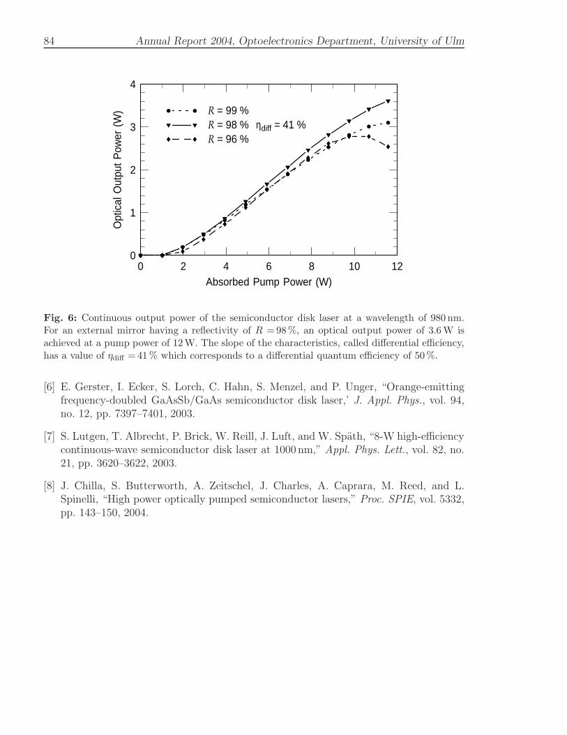
84 Annual Report 2004, Optoelectronics Department, University of Ulm
0 2 4 6 8 10 120
1
2
3
4
Absorbed Pump Power (W)
Opt
ical
Out
put
Pow
er (
W) R = 99 %
R = 98 % ηdiff = 41 % R = 96 %
Fig. 6: Continuous output power of the semiconductor disk laser at a wavelength of 980 nm.For an external mirror having a reflectivity of R = 98 %, an optical output power of 3.6 W isachieved at a pump power of 12 W. The slope of the characteristics, called differential efficiency,has a value of ηdiff = 41 % which corresponds to a differential quantum efficiency of 50 %.
[6] E. Gerster, I. Ecker, S. Lorch, C. Hahn, S. Menzel, and P. Unger, “Orange-emittingfrequency-doubled GaAsSb/GaAs semiconductor disk laser,’ J. Appl. Phys., vol. 94,no. 12, pp. 7397–7401, 2003.
[7] S. Lutgen, T. Albrecht, P. Brick, W. Reill, J. Luft, and W. Spath, “8-W high-efficiencycontinuous-wave semiconductor disk laser at 1000 nm,” Appl. Phys. Lett., vol. 82, no.21, pp. 3620–3622, 2003.
[8] J. Chilla, S. Butterworth, A. Zeitschel, J. Charles, A. Caprara, M. Reed, and L.Spinelli, “High power optically pumped semiconductor lasers,” Proc. SPIE, vol. 5332,pp. 143–150, 2004.

Optimization of Process Parameters for Low-Absorbing Optical Coatings 85
Optimization of Process Parameters for
Low-Absorbing Optical Coatings Fabricated by
Reactive Ion-Beam Sputter Deposition
Steffen Lorch
The parameters of a reactive ion-beam sputter deposition system have to be optimized toachive layers with low absorption. For that, different materials have been deposited withvariing the oxygen partial pressure to find the optimum for each material. Additionally,the position and the angle of the substrate related to the target have been changed toexamine the influence on the absorption. The measurements have been performed usingphotothermal deflection which is a suitable method to determine such small absorptionvalues.
1. Introduction
Optical coatings have a wide range of applications. For lasers, anti-reflection/highreflectioncoatings are used and laser amplifiers need coatings with reflectivities lower than 10−4,additionally they should have a very low absorption to increase the threshold of thecatastrophically optical mirrow damage (COMD). Low absorptions are also necessary forcoatings on disk lasers because they are located in the cavity and, due to multi passes ofthe light, absorbing layers can inhibit lasing. To achieve optical coatings with low absorp-tion, a reactive ion-beam sputter deposition (RIBSD) system is used because of the denseand stoichiometric layers [1, 2, 3, 4]. To optimize the coating parameters of such a sys-tem, the absorption of the coated layers has to be measured. For that, the photothermaldeflection method [5, 6] has been used to measure such low absorption values.
2. Theory
The sputter process of a RIBSD system is schematically shown in Fig. 1. The argonions are extracted from an ion-beam source, are neutralized by electrons, and strike thetarget. The sputtered target material is deposited on the substrate. During the sputterprocess, a part of the oxygen is lost (1) and the deposited material is understoichiometric,this results in absorbing layers. To avoid this, additional oxygen is introduced into theprocess chamber to increase the oxide state of the target and so the deposited materialis stoichiometric and has a lower absorption. But with increasing the partial pressureof oxygen the absorption increases due to the higher amount of high-energetic oxygen

86 Annual Report 2004, Optoelectronics Department, University of Ulm
+Ar+Ar
2O
−e
Substrate
Neutralizer
Target
Ion−BeamSource
(1)(2)
Fig. 1: Schematical drawing of the sput-ter mechanism. Possible absorption may becaused by insufficient oxygen (1) and dam-age by high-energetic oxygen (2).
0.0 0.2 0.4 0.6 0.8 1.0 1.20.0
0.2
0.4
0.6
0.8
1.0
O2–flow (sccm)
Abs
orpt
ion
(a.u
.)
not stoichiometric insufficient oxygen (1)
more damage by high–energetic oxygen (2)
Theory
Fig. 2: Theoretical curve for the absorptionover the oxygen partial pressure and the lim-iting effects.
bombardment (2) which brings damage on the deposited material. Thus, the absorptionis a superposition of these two mechanisms and at the optimal partial pressure of oxygen,the absorption shows a minimum. This behavior is theoretically depicted in Fig. 2 [2].
3. Measurement Method
The absorption of metal-oxide coatings fabricated with reactive ion-beam sputter deposi-tion has values in the range of α ≈ 1 cm−1 (k = 10−5 or 10 ppm for 100nm) and less. Tomeasure such low values, the photothermal deflection method is used [5, 6]. In Fig. 3, thesetup is depicted. The sample (coated layer on a glass substrate) is placed in a cuvettefilled with CCl4, which is mounted on an x–y stage. The choppered pump beam (45mWlaser at 685 nm, placed on a z stage) passes the sample perpendicularly and, due to theabsorption in the layer, heat is generated. This results in a temperature gradient in theCCl4 and thus in a gradient of the refractive index (dn/dTCCl4 = 6.4 · 10−4). A probe beam(5mW laser at 633 nm) passes the sample parallel near the surface, is deflected by thegradient of the refractive index, and the deflection angle is measured with a 4-quadrantphoto diode and a lock-in amplifier. The position of the pump and the probe beam tothe sample is very critical and all parameters (x, y, and z) should be optimized to get amaximum in the signal.
The result for such a measurement (here exemplarily for Al2O3) is shown in Fig. 4. Thethickness (deposition rate) and the refractive index are measured with an ellipsometer(633 nm). It can be seen that the deposition rate decreases with increasing the oxygenflow or rather the partial pressure. The refractive index shows a fast decrease and thenstays constant with increasing the oxygen flow. The absorption is measured with thephotothermal deflection and the curve looks similar to the theoretical one in Fig 2. Withno oxygen in the chamber, the absorption is relatively high and decreases with a small

Optimization of Process Parameters for Low-Absorbing Optical Coatings 87
Z Y
X Glass with
Pump Beam
Deflection
CClRefractive IndexGradient of Angle
4
CoatingProbeBeam
Fig. 3: Schematic view of the photothermaldeflection measurement method.
0.0 0.5 1.0 1.5 2.01.30
1.35
1.40
1.45
1.50
1.550 0.5 1.0 1.5
Oxygen Flow (sccm)
Dep
ositi
on R
ate
(nm
/min
)
O2 Partial Pressure (10–5 mbar)
Al2O3
0.0 0.5 1.0 1.5 2.0
1.67
1.68
1.69
Ref
ract
ive
Inde
x
0
2
4
6
8
Abs
orpt
ion
(a.u
.)
Rate n α
Fig. 4: Deposition rate, refractive index,and absorption depending on the oxygenpartial pressure.
amount of oxygen. But with a higher oxygen flow the absorption starts to increase again.A minimum in the absorption can be found where the coating process should operate.
4. Measurement Results
The reactive ion-beam sputter deposition system used for these experiments has an in-ductively coupled plasma (ICP) ion-beam source and a water-cooled target holder forfour targets. The following results are achieved with an ion-beam current of IB=40mA,a beam voltage of UB=1000V, and an acceleration voltage of UB=120V. Four differentmaterials have been examined and the substrate position has been optimized.
4.1 Oxygen dependent absorption for different materials
For four different materials (SiO2, Al2O3, Y2O3, and Ta2O5), the measurement of thedeposition rate, the refractive index and the absorption has been performed as describedbefore (see Fig. 4). The absorption of the different materials depending on the oxygenpartial pressure can be seen in Fig. 5. Every material shows the same behavior, at low andhigh oxygen partial pressures a high absorption, and at a certain pressure a minimum.The difference of the value and the position varies with the material and also can beinfluenced by parameters like e. g. ion-beam current or total pressure.
In Fig. 6, the spectral refractive index of the four examined materials is shown. This valueswere measured and extracted with spectral ellipsometry [7] at L.O.T.-Oriel GmbH & Co KG.

88 Annual Report 2004, Optoelectronics Department, University of Ulm
0.0 0.5 1.0 1.5 2.0 2.5 3.0 3.50
2
4
6
8
10
12
14
O2 Partial Pressure (10–5mbar)
Abs
orpt
ion
(a.u
.)
Al2O3 Ta2O5
SiO2
Y2O3
Fig. 5: Absorption over oxygen partial pres-sure for different materials.
300 400 500 600 700 800 900 10001.4
1.6
1.8
2.0
2.2
2.4
2.6
Wavelength (nm)
Ref
ract
ive
Inde
x
Ta2O5
Y2O3
Al2O3
SiO2
Fig. 6: Refractive index over wavelength fordifferent materials determined with spectralellipsometry.
4.2 Substrate position
In this section, the substrate position has been changed to optimize the coating parame-ters. For these experiments, only one material (Ta2O5) has been examined.
In Fig. 7, a schematic view of the system configuration in the x–z plane is shown. TheAr+ ion beam strikes the target under an angle of 55 and the target normal is tilted 5
against the normal of the substrate. The reflected Ar+ ions have about the same anglelike the incident ions. The sputtered material, in contrast, leaves the target more or lessperpendicular.
−5 0 5 10Y
Z
X (cm)
Substrate
Ar+
Target
SputteredMaterial Reflected
Ions
Fig. 7: Schematic view of the sputter sys-tem in the x–z plane.
–4 –2 0 2 4 6 8 10
2.8
3.0
3.2
3.4
3.6
Substrate Position (cm)
Dep
ositi
on R
ate
(nm
/min
)
–4 –2 0 2 4 6 8 10
2.16
2.18
2.20
2.22
Ref
ract
ive
Inde
x
0
5
10
15
Abs
orpt
ion
(a.u
.)
Fig. 8: Deposition rate, refractive index,and absorption depending on the substrateposition for Ta2O5.
In Fig. 8, the results for different substrate positions on the x axis are shown. Withincreasing the x position the deposition rate increases and shows a plateau between 2and 6 cm, in this region the homogeneity is quite good (±1.5%). The absorption has a

Optimization of Process Parameters for Low-Absorbing Optical Coatings 89
minimum between -1 and 3 cm and increases rapidly to higher x values due to the dis-turbance of the reflected Ar+ ions in this range. Also the refractive index behaves likethe absorption and has for x ≤ 6 cm a quite constant value with a deviation of less than±0.25%. This results point out that the system is well designed and there is a windowfor the substrate position which shows a low absorption and a good homogeneity.
In Fig. 9, the system is shown in the y–z plane; the Ar+ ion beam enters the plane fromviewers point. The normal of the substrate can be varied against the normal of the tar-get, at an angle of α = 0, substrate and target are parallel in the y–z plane. There arethree faces indicated. For example face a (parallel to the substrate) can be the facet ofa laser, so face b and c (perpendicular to the substrate) are the n and p contact of the laser.
Z
b
c a
α
Y
X
Substrate Target
SputteredMaterial
Fig. 9: Schematic view of the sputter sys-tem in the y–z plane.
0 10 20 30 40
0.0
1.0
2.0
3.0
4.0
Substrate Angle (°)
Dep
ositi
on R
ate
(nm
/min
)
a
b
cos α sin α
0 10 20 30 40
2.16
2.18
2.20
2.22
Ref
ract
ive
Inde
x
0
5
10
15
Abs
orpt
ion
(a.u
.)
Fig. 10: Deposition rate, refractive index,and absorption depending on the substrateangle for Ta2O5.
Figure 10 shows, that the deposition rate of the face a decreases with increasing substrateangle, just like a cosine function; the face b, in opposite, increases just like a sine function.Face c decreases and at 10 no material is deposited anymore (not shown in the graph).In such a case one contact of a laser is not deposited and can be mounted without loosingthermal conductivity. The absorption shows a minimum in the range of 0 to 20 butbeyond this angle it increases rapidly. The refractive index has a low deviation of ±0.3%in this low-angle range. This results show, that the angle of the substrate can be varied inthe range of 0 to 20 without decreasing the quality of the coating but with preventingone face, e. g. of a laser, from getting deposited.
5. Conclusion
By using the photothermal deflection method, the absorption of coated layers has beenmeasured and the process parameters have been optimized. During the sputter process,oxygen has to be introduced into the chamber to achieve stoichiometric and dense layers.

90 Annual Report 2004, Optoelectronics Department, University of Ulm
For four different materials, the optimized amount of oxygen to get minimum absorptionhas been figured out. The substrate position has been varied and there is range withminimum absorption and a good homogeneity. Also the substrate angle can be changedin a small range to prevent the perpendicular face from being coated and, simultaneous,keep a low value of the absorption.
References
[1] F.R. Flory, Thin films for optical systems, vol. 49. New York: Dekker, 1. ed., 1995.
[2] M. Tilsch, Eigenschaften ionenstrahlgesputterter optischer SiO2- and TiO2- Schichtenbei unterschiedlichen Wachstumsbedingungen und Veranderungen bei thermischerNachbehandlung. PhD thesis, University of Darmstadt, Darmstadt, Germany, Jan.1997.
[3] J. Becker, “Ion-beam sputtering,” ch. 7 in Handbook of optical properties. Volume I:Thin films for optical coatings, R.E. Hummel and K.H. Guenther (Ed.), Boca Raton:CRC Press, pp. 189–212, 1995.
[4] D.T. Wei, H.R. Kaufman, and C.-C. Lee, “Ion beam sputtering,” ch. 6 in Thin filmsfor optical systems, F.R. Flory (Ed.), New York: Marcel Dekker, pp. 133–201, 1995.
[5] W.B. Jackson, N.M. Amer, A.C. Boccara, and D. Fournier, “Photothermal deflectionspectroscopy and detection,” Appl. Optics, vol. 20, no. 8, pp. 1333–1344, 1981.
[6] E. Welsch and D. Ristau, “Photothermal measurements on optical thin films,” Appl.Optics, vol. 34, no. 31, pp. 7239–7253, 1995.
[7] D.E. Aspnes, “The accurate determination of optical properties by ellipsometry,” ch.5 in Handbook of optical constants of solids, E.D. Palik (Ed.), Orlando: AcademicPress, pp. 89–112, 1985.

External-Cavity Tapered Semiconductor Ring Lasers 91
External-Cavity Tapered Semiconductor Ring Lasers
Frank Demaria
Laser operation of a tapered semiconductor amplifier in a ring-oscillator configurationis presented. In first experiments, 1.75W time-average optical output power has beenachieved at room temperature. Results for different configurations and feedback ratiosare shown and compared to the output characteristics of the same device in a master-oscillator power-amplifier configuration. Dynamical analysis of the optical signal revealspassively mode-locked operation. The repetition rate of the generated pulses of 214MHzis determined by the round-trip time of 4.67 ns. Fourier-transformation of the frequencysignal to the time-domain yields a pulse-duration of less than 80 ps.
1. Introduction
Tapered travelling-wave laser-amplifiers usually are part of a master-oscillator power-amplifier setup. Typical for such devices is the very low reflectivity of the facets, whichis in the range of 10−4. Besides the use of anti-reflection coatings, bent ridge-waveguides,which hit the facet under a tilt angle with respect to the normal, can be utilized to lowerthe residual reflectivity [1]. On the other hand, the same kind of device is often designedas a laser oscillator with a linear resonator, by applying mirrors in the form of coatingswith higher reflectivities [2], DBR-mirrors [3][4], or by external mirrors which can berealized also in a wavelength selective version, using a grating in order to make the lasertunable [5]. Beyond that, the use of a tilted-stripe taveling-wave optical amplifier in aexternal-cavity ring laser setup has already been demonstrated [6].
Instead of a traveling-wave optical amplifier with stripe-geometry, we used a device havinga tapered gain region in a ring laser setup. The astigmatism, or with other words, theposition of the internal virtual source of a tapered amplifier strongly depends strongly onits saturation. With the setup presented here, an image of the internal virtual source isprojected onto the input facet of the amplifier, which acts as a spatial mode filter. With asuitable alignment, only the emission of the highly saturated amplifier is efficiently coupledback into the amplifier. By that way, a saturable absorption mechanism is established.It is important to note, that this is only possible for the ring-resonator configurationof a tapered amplifier but not for any kind of linear resonator nor for stripe-geometryamplifiers in a ring resonator. The described behaviour is quite analog to kerr-lens modelocking (KLM) which is commonly utilized for the passive mode locking of solid-statelasers.

92 Annual Report 2004, Optoelectronics Department, University of Ulm
2. Device and Setup
Faraday−Isolator
SplitterBeam−
CylindricalLens
Amplifier
Mirror 1
Mirror 2
Fig. 1: Setup of the ring oscillator configuration with a tapered semiconductor laser amplifier.The aspherical lenses at the left (f = 4.5 mm) and at the right side (f = 6.5 mm) of the amplifierare collimating the beam in the fast-axis direction, which is pependicular to the drawing plane.The cylindrical lens with a focal length of 100 mm is necessary to compensate the astigmatismof the amplifer and to collimate the beam in the slow-axis direction.
Figure 1 shows the schematic diagram of the ring-oscillator setup. The laser active deviceis a 2.5mm long tapered semiconductor amplifier with a 500µm-long and 3.5 µm-wideridge waveguide. The maximum gain of the amplifier at room temperature is at 920 nm.The geometrical round-trip length of the resonator is 1260mm. By a Faraday isolator,clockwise circulation is ensured, which is essential, as only the broad output facet of theamplifier, which is orientated to the right side in Fig. 1, can withstand high optical powersof several watts, due to its width of 210µm. The laser light which is emitted from thisfacet is collimated in the direction of the fast axis, which is perpendicular to the drawingplane, by a collimating lens system with a focal length of 6.5mm and a high numericalaperture of 0.615. Because of the astigmatism of the tapered gain region, the verticallycollimated beam is convergent in the horizontal direction and forms a intermediate focusthere. At an adequate distance right after the intermediate focus, a 100mm focal lengthcylindrical lens is located, in order to collimate the beam also in the horizontal direction.With a beam-splitter a 16.5% fraction of the optical power is branched off in order tobe fed back into the amplifier. The reflected beam is passing through a Faraday isolatorand by two gold mirrors directed versus the input facet, to which the beam is focussed bya 4.5mm-focal-length aspherical lens with a numerical aperture of 0.55. The bent ridgewavegide in the input section of the device meets the input facet under 4.5, thus theincident angle of the beam has to be 15 due to the waveguide’s high effective refractiveindex.
One severe practical problem is regarding the alignment of the optical components.Namely, that the beam can not be observed inside the resonator with a detector card, cam-era or scanning-slit system. With such a optical barrier inside the resonator, the amplifier

External-Cavity Tapered Semiconductor Ring Lasers 93
will switch to its non-feedback operation mode, where amplified spontaneous emission isdominant and the beam propagation is completely different compared to laser operation.In order to overcome that problem, we first coupled a signal from a master-oscillator intothe amplifier, to perform an alignment and suitable collimation of the emitted beam. Alloptical components except Mirror 1 can be positioned and adjusted by that way. In afinal step, the additon of Mirror 1 and its alignment can be performed easily.
3. Experimental Results
3.1 Quasi-statical behaviour
At first, the optical output of the ring oscillator was measured with a thermophile powerdetector. Despite this kind of detector is quite reliable for the measurement of opticalpowers of several watts, it has a multi second response time, therefore the optical powerswhich are presented in this subsection should always be mentioned to be long time aver-aged. Additionally, in Subsection 3.2 the results of the experimental investigation of thedynamical behavior will be presented.
As the threshold current depends on the feedback ratio, this can be affected by the useof beam-splitters with various splitting ratios. Figure 2 shows that for two differentreflection ratios of 16.5% and 4%. For the lower reflectivity, we observed a less stableoperation that led to deviatons in the corresponding graph. The tapered amplifer has
Fig. 2: Output characteristics with different beam splitting reflectivities.
also been characterized in a master-oscillator power-amplifier setup, where the emissionof a single-mode ridge-waveguide laser has been used as a input signal. In Fig. 3 this

94 Annual Report 2004, Optoelectronics Department, University of Ulm
output characteristics with an optical input power of 10mW is compared to that of thering-oscillator setup. To demonstrate that the feedback was not established by any kindof a parasitical linear resonator, we interrupted the feedback path at different locationsand measured the optical output with no feedback, which was constantly low in all cases.The corresponding graph in Fig. 3 reveals the difference to the case with feedback.
Fig. 3: Comparison of the optical output characterisics of the tapered laser in a master-oscillatorpower amplifier setup, and the same device in a ring laser configuration.
3.2 Dynamical behaviour
Because of the anticipated high repetiton rate and low pulse duration time, the timedependency can not simply be observed by a normal oscilloscope. Furthermore the lackof a trigger signal makes this measurement even more difficult. To decide whether thelaser is runnig in constant-wave or pulsed mode, the electrical signal from a photo diodewas analized with respect to its spectral behavior.
As Fig. 4 shows, this analysis reveals a distinct equidistant spectral coverage with har-monics over the whole measurement range from 0 to 20GHz. The limitation to 20GHzis due to the measurement-setup. For this measurement, the averaged optical power was1.05W at a current of 3.5A. Harmonics can be observed over a wide range of differentcurrents. The adjustment of the resonator was performed in order to achieve a high aver-aged optical power and distinct harmonics over the whole spectral range at the same time.Generally, the distribution and intensity of the harmonics depends on the adjustment ofthe feedback coupling. The separation of the different harmonics of 214MHz correspondsto an optical round-trip length of 1.40m. The spectral signal is Fourier-transformed to

External-Cavity Tapered Semiconductor Ring Lasers 95
Fig. 4: Measured electrical spectrum of the time dependend ring-laser signal. The time averagedoptical power is 1.05 W at a current of 3.5 A.
Fig. 5: Time signal reproduction by Fourier-transformation of the electrical signal from Fig. 4
the time domain numerically. The result is given in Fig. 5. The distinct peaks have arepetition time of 4.67 ns and a duration of less than 80 ps.
4. Conclusion and Discussion
For the first time, the use of a tapered semiconductor laser-amplifier, in a quite simplesetup as a ring-oscillator and its capability of generating pico-second laser pulses by passivemodelocking is demonstrated. The presented characteristics should be regarded as “firstresults”. From the averaged optical output power of 1.05W, an amplified spontaneousemission power of 0.15W and a duty cycle of less than 1:58, the peak power can beestimated to be at least 50W, considering the fact that the measured pulse durationis limited by the bandwidth of the employed photo-diode. As a limiting factor for thereal pulse duration time, the dispersion which is introduded by the amplifier should bementioned and possibly compensated in a more improved setup. Together with the highspatial beam quality of tapered laser devices, the high peak power makes such a systeman interesting laser source for the generation of pulses and second harmonic generation.
96 Annual Report 2004, Optoelectronics Department, University of Ulm
References
[1] M. Mundbrod, “Ridge-waveguide lasers with tiltet facets,” Annual Report 2003, Dept.of Optoelectronics, University of Ulm.
[2] H. Wenzel, B. Sumpf, G. Erbert, “High-brightness diode lasers”, C. R. Physique,vol. 4, pp. 649–661, 2003.
[3] D. Mehuys, S. O’Brien, R.J. Lang, A. Hardy, D.F. Welch ”5W, diffraction-limited,tapered-stripe unstable resonator semiconductor laser”, Electron. Lett., vol. 30, no. 22,pp. 1855–1856, 1994.
[4] S.R. Semic, G.A. Evans, T.M. Chou, J.B. Kirk, J.N. Walpole, J.P. Donelly, C.T. Har-ris, L.J. Missaggia, “Single Frequency 1550-nm AlGaInAs-InP Tapered High-PowerLaser With a Distributed Bragg Reflector”, IEEE Photon. Technol. Lett., vol. 14,no. 7, pp. 890–892, 2004
[5] S. Morgott, P. Charzan, M. Mikulla, M. Walther, R. Kiefer, R. Kiefer, J. Braunstein,G. Weimann, ”High-power near-diffraction-limited external cavity laser, tunable from1030 to 1085 nm”, Electron. Lett., vol. 34, no. 6, pp. 558–559, 1998.
[6] En T. Peng, C. B. Su,”Properties of an external-cavity traveling-wave semicondudtorring laser”, Opt. Lett., vol. 17, no. 1, 1992.

Ph.D. Thesis 97
Ph.D. Theses
1. Marcus Andreas Scherer,Prozesstechnologie fur GaN-basierende Leuchtdioden,January 2004.
2. Irene Ecker,Molekularstrahlepitaxie GaAs-basierender Mischungshalbleiter fur 1300 nm-nahe Laser-diodenemission,January 2004.
3. Matthias Golling,Molekularstrahlepitaxie vertikal emittierender InGaAs-Laser-Strukturen mit periodi-scher Gewinnstruktur,March 2004.
4. Jurgen Joos,Technologien zur Realisierung langwellig emittierender Vertikallaserdioden,July 2004.

98 Annual Report 2004, Optoelectronics Department, University of Ulm
Diploma and Master Theses
1. Peter Bruckner,Einfluß der Prozeßparameter beim epitaktischen Uberwachsen von strukturiertenGaN-Schichten mittels MOVPE,Diploma Thesis, Optoelectronics Department, January 2004.
2. Antonia Reeg,Aufbau eines Empfangsmoduls zur optischen Freiraumdatenkommunikation zwischenFahrzeugen,Diploma Thesis, Optoelectronics Department, February 2004.
3. Christof Jalics,Entwicklung und Untersuchung von Prozessen zur Herstellung von VCSELn mitdielektrischen Oberflachengittern zur Polarisationskontrolle,Diploma Thesis, Optoelectronics Department, March 2004.
4. Markus Thal,Erstellung eines Messplatzes zur Bestimmung der Zuverlassigkeit von PIN-Photodiodenfur die optische Datenubertragung,Diploma Thesis, Optoelectronics Department, March 2004.
5. Martin Feneberg,Untersuchung von VCSELn mit einem dielektrischen OberflachengitterDiploma Thesis, Optoelectronics Department, May 2004.
6. Michael Schumann,Prozessierung und Charakterisierung von kurzwelligen Laserdioden im Materialsys-tem AlGaAs,Diploma Thesis, Optoelectronics Department, May 2004.
7. Heiko Paul,n- und p-Dotierung von AlGaN mittels MOVPE,Diploma Thesis, Optoelectronics Department, July 2004.
8. Hayssam El- Hajj,Bended Waveguide Semiconductor Laser Amplifiers,Master Thesis, Optoelectronics Department, August 2004.
9. Onur Atilla,Minimization of the Absorption of Optical Coatings Using Photothermal DeflectionSpectroscopy,Master Thesis, Optoelectronics Department, August 2004.
10. Tobias Fischer,Transistor- und Diodenmodelle fur Hochspannungs-CMOS-Prozesse mit Trenchisolierung,Diploma Thesis, Optoelectronics Department, August 2004.

Diploma and Master Theses 99
11. Lutz Stoferle,Untersuchung und Optimierung von Komponenten eines bidirektionalen optischenUbertragungssystems bei 850 nm Wellenlange,Diploma Thesis, Optoelectronics Department, December 2004.

100 Annual Report 2004, Optoelectronics Department, University of Ulm
Semester Projects
1. Johanna May,Internal quantum efficiency of thin film solar cells on wafer and glass substrates —Measurement and simulation,May 2004,
2. Lutz Stoferle,Untersuchung zu temperaturabhangigen Eigenschaften von Metall-Halbleiter-Metall(MSM)-Photodioden,June 2004,
3. Thomas Wunderer,Optimierung der Montagetechnik GaN-basierender Laserdioden,August 2004
4. Joachim Hertkorn,Einsatz von Vertikal emittierenden Laserdioden in der optischen Partikeldetektion,November 2004,
5. Gregor Wendrock,Berechnungen zur optischen Leistungseinkopplung von Vertikallasern in Gradien-tenindexfasern,December 2004

Talks 101
Talks
[1] P. Bruckner, F. Habel, and F. Scholz, “Epitaxie von defektreduzierten GaNSchichten”, 19. DGKK-Workshop Epitaxie von III/V-Halbleitern, Freiburg i. Br.Germany, Dec. 2004.
[2] E. Gerster, “Intra-Cavity Frequency-Doubled Semiconductor Disk Laser Based onGaAsSb/GaAs”, ETH Zurich, Switzerland, Dec. 2004.
[3] C. Kirchner, P. Bruckner, and F. Scholz, “Wachstum hoch Al-haltiger AlGaN- undAlN-Schichten mit MOVPE”, 19. DGKK-Workshop Epitaxie von III/V-Halbleitern,Freiburg i. Br. Germany, Dec. 2004.
[4] R. Michalzik, “High-power semiconductor lasers: from horizontal to vertical cavities”,Center for Photonic Materials & Devices, Chonnam National University, Gwangju,Korea, June 2004.
[5] R. Michalzik, “Recent topics in short-wavelength VCSEL research”, Gwangju Insti-tute of Science and Technology (GIST), Dept. of Materials Sci. & Eng., Gwangju,Korea, June 2004.
[6] R. Michalzik, “Ulm University and the cleanroom of the Faculty of EngineeringScience”, Dongshin University (DSU), School of Health Science and Welfares, Dept.of Biomedical Engineering, Naju, Chonnam, Korea, June 2004.
[7] R. Michalzik, “VCSEL based optical interconnects”, Gwangju Institute of Scienceand Technology (GIST), Dept. of Information & Communications, Gwangju, Korea,June 2004.
[8] R. Michalzik, “Modern semiconductor lasers and communication applications”,Physics Colloquium of El Minia University, Minia, Egypt, Feb. 2004.
[9] R. Michalzik, “Vertical-cavity surface-emitting laser diodes for optical interconnects”(in German), Technical Physics Seminar of Wurzburg University, Wurzburg, Ger-many, Jan. 2004.
[10] B. Neubert, F. Habel, P. Bruckner, F. Scholz, T. Riemann, and J. Christen, “Elek-trolumineszenz von GaInN-Quantenfilmen auf Facetten von selektiv gewachsenenGaN-Streifen”, 19. DGKK-Workshop Epitaxie von III/V-Halbleitern, Freiburg i. Br.Germany, Dec. 2004.
[11] J.M. Ostermann, “Current Research at the Optoelectronics Department, Universityof Ulm,” Chalmers University, Group Seminar of the Photonics Lab, Gothenborg,Sweden, Aug. 2004.

102 Annual Report 2004, Optoelectronics Department, University of Ulm
[12] J.M. Ostermann, P. Debernardi, A. Haglund, G.P. Bava, A. Larsson, R. Michalzik,“VCSELs with an integrated grating relief for single-polarization and single-modeemission,” European Semiconductor Laser Workshop, Saro, Sweden, Aug. 2004.
[13] J.M. Ostermann, “Diffractive Optics for Polarization Control of Vertical-CavitySurface-Emitting Lasers (VCSELs),” Westfalische Wilhelms-Universitat Munster, In-stitut fur angewandte Physik, Group Seminar of the AG Nichtlineare Optik undQuantenoptik, Munster, Germany, Nov. 2004.
[14] F. Rinaldi, “Epitaxy and Characterization of Semiconductor Disk Lasers”, DeutscherMBE-Workshop, Physikalisch-Technische Bundesanstalt, Braunschweig, Germany,Oct. 2004.
[15] F. Scholz, “Crystalline interfaces and Strain in Compound Semiconductors”, Work-shop of Graduiertenkolleg “Interfaces in Crystalline Materials”, Ellwangen. Feb.2004.
[16] F. Scholz, F. Habel, and P. Bruckner, “Defektreduzierung in GaN fur optoelektron-ische Anwendungen”, Seminar talk Uni/IAF Freiburg, June 2004.
[17] F. Scholz, F. Habel, and P. Bruckner, “Preparation of GaN quasi substrates by HVPEand MOVPE”, Aixtron User Meetings, Hsinshu and Tainan, Taiwan, Sept. 2004.
[18] F. Scholz, “Optoelectronics in Germany - an attempt to describe the current situa-tion”, Talk at Wuhan University of Science & Engineering, China, Oct. 2004.
[19] F. Scholz, “Studies at the faculty of Engineering at Ulm University”, Talk at WuhanUniversity of Science & Engineering, China, Oct. 2004.
[20] F. Scholz, F. Habel, and P. Bruckner, “Defect reduction in GaN structures on sap-phire”, OSRAM OS GaN Workshop Schloss Hohenkammer, Nov. 2004.
[21] F. Scholz, “GaN in neuen Spektralbereichen: Materialtechnische Herausforderungenund Grenzen”, 2. Fachtagung Innovative Beleuchtung, Dusseldorf, Nov. 2004.
[22] P. Unger, “Halbleiter-Scheibenlaser”, Ferdinand-Braun-Institut fur Hochstfrequenz-technik (FBH), Berlin , May 2004.
[23] P. Unger, “Semiconductor Disk Lasers”, Bookham Laser Enterprise, Zurich, Switzer-land, July 2004.
[24] P. Unger, “Optically Pumped Semiconductor Disk Lasers”, Emerging Technologiesin Optical Sciences (ETOS) 2004, Cork, Ireland, July 2004.
[25] P. Unger, “Optically Pumped Semiconductor Disk Lasers”, Universite de Neuchatel,Neuchatel, Switzerland, Dec. 2004.

Publications and Conference Contributions 103
Publications and Conference Contributions
[1] C. Eichler, D. Hofstetter, W.W. Chow, S. Miller, A. Weimar, A. Lell, and V. Harle,“Microsecond time scale lateral-mode dynamics in a narrow stripe InGaN laser”,Applied Physics Letters, vol. 84, pp. 2473–2475, 2004.
[2] C. Eichler, S.S. Schad, F. Scholz, S. Miller, A. Leber, A. Lell, and V. Harle, “TimeDependent Modal Behaviour of InGaN-based laser diodes”, International Workshopon Nitride Semiconductors, IWN 2004, Pittsburgh, PA, USA, July 2004.
[3] P. Gerlach, M. Peschke, and R. Michalzik, “High-frequency performance optimizationof DFB laser integrated electroabsorption modulators”, in Proc. Semiconductor andIntegrated Optoelectronics Conf., SIOE 2004, paper 41. Cardiff, Wales, UK, Apr.2004.
[4] E. Gerster, S. Menzel, and P. Unger, “Intra-cavity frequency-doubled semiconductordisk laser based on GaAsSb/GaAs,” European Semiconductor Laser Workshop 2004,Saro, Sweden, Sep. 2004.
[5] F. Habel, P. Bruckner, and F. Scholz, “Marker layers for the development of a mul-tistep GaN FACELO process”, 12th Int’l Conference on Metal Organic Vapor PhaseEpitaxy, ICMOVPE XII, Lahaina, Hawaii, USA, J. Crystal Growth, vol. 272, pp.515–519, 2004.
[6] F. Habel, P. Bruckner, J.D. Tsay, W.Y. Liu, F. Scholz, D. Schmitz, A. Alam, and M.Heuken, “Hydride vapor phase epitaxial growth of thick GaN layers with improvedsurface flatness”, International Workshop on Nitride Semiconductors, IWN 2004,Pittsburgh, PA, USA, July 2004, phys. stat. sol. (c) DOI: 10.1002, 2005.
[7] R. Michalzik, “Vertical-cavity surface-emitting lasers for optical interconnects” (in-vited), in Proc. XXIV Conf. on Solid State Physics and Materials Science of theEgyptian Materials Research Society, Eg-MRS 2004 & Workshop on Photonic Ma-terials and Optoelectronic Devices, p. 23. Safaga, Red Sea, Egypt, Febr. 2004.
[8] R. Michalzik, J.M. Ostermann, P. Debernardi, C. Jalics, A. Kroner, M. Feneberg, andM. Riedl, “Polarization-controlled monolithic oxide-confined VCSELs” (invited), inMicro-Optics, VCSELs and Photonic Interconnects, H. Thienpont, K.D. Choquette,M.R. Taghizadeh (Eds.), Proc. SPIE 5453, pp. 182–196, 2004.
[9] R. Michalzik, K.J. Ebeling, M. Kicherer, F. Mederer, R. King, H. Unold, and R.Jager, “High-performance VCSELs for optical data links”, in High-PerformanceBackbone Network Technologies, N. Yamanaka (Ed.), pp. 1005–1013. New York:Marcel Dekker, Inc., 2004. Previously published in IEICE Trans. Commun., vol.E84-B, pp. 1255–1264, 2001. Also published in IEICE Trans. Electron., vol. E84-C,pp. 629–638, 2001.

104 Annual Report 2004, Optoelectronics Department, University of Ulm
[10] B. Neubert, F. Habel, P. Bruckner, F. Scholz, T. Riemann, and J. Christen, “Electro-luminescence from GaInN quantum wells grown on non-(0001) facets of selectivelygrown GaN stripes”, MRS Fall Meeting 2004, paper E11.32., Boston, MA, USA,Nov. 2004, accepted for publication in MRS Symp. Proc. GaN, AlN, InN, and TheirAlloys, 2005.
[11] J.M. Ostermann, P. Debernardi, C. Jalics, A. Kroner, M. Feneberg, M. Riedl, andR. Michalzik, “Monolithic polarization control of multimode VCSELs by a dielectricsurface grating”, in Vertical-Cavity Surface-Emitting Lasers VIII, C. Lei and S.P.Kilcoyne (Eds.), Proc. SPIE 5364, pp. 201–212, 2004.
[12] J.M. Ostermann, P. Debernardi, C. Jalics, M. Feneberg, A. Kroner, M.C.Riedl, M. Golling, and R. Michalzik, “High single-mode power, monolithicpolarization-controlled oxide-confined grating relief VCSELs”, in Proc. 19th IEEEInt.’l Semicond. Laser Conf., pp. 109–110. Kunibiki Messe, Matsue-shi, SimanePref., Japan, Sept. 2004. For corrections see URL http://www-opto.e-technik.uni-ulm.de/forschung/ram/pub/islc2004.html .
[13] M. Peschke, P. Gerlach, B. Saravanan and B. Stegmuller, “Thermal crosstalk inintegrated laser-modulators”, IEEE Photon. Technol. Lett., vol. 16, no. 11, pp. 2508–2510, 2004.
[14] M. Peschke, B. Saravanan, C. Hanke, T. Knodl, and B. Stegmuller, “Investigationof the capacitance of integrated DFB-EAMs with shared active layer for 40GHzbandwidth”, in Proc. IEEE Lasers and Electro-Opt. Soc. Ann. Meet., LEOS 2004,pp. 673–674. San Juan, Puerto Rico, Nov. 2004.
[15] H. Roscher and R. Michalzik, “Toward redundant 2-D VCSEL arrays for optical dat-acom”, in Micro-Optics, VCSELs and Photonic Interconnects, H. Thienpont, K.D.Choquette, M.R. Taghizadeh (Eds.), Proc. SPIE 5453, pp. 170–181, 2004.
[16] S.S. Schad, B. Neubert, J. Bruning, C. Eichler, F. Habel, F. Scholz, P. Unger, and D.Hofstetter, “Absorption in InGaN-on-sapphire LED-structures: Comparison betweenthe Photocurrent Measurement Method (PMM) and the Photothermal DeflectionSpectroscopy” in Light Emitting Diodes: Research, Manufacturing, and Applications,E.F. Schubert (Ed.), Proc. SPIE 5336, 2004.
[17] S.S. Schad, B. Neubert, C. Eichler, M. Scherer, F. Habel, M. Seyboth, F. Scholz,D. Hofstetter, P. Unger, W. Schmid, C. Karnutsch, and K. Streubel, “Absorptionand light scattering in GaN-on-sapphire- and AlGaInP-based light-emitting-diodes”,IEEE J. Lightwave Technol., vol. 22, pp. 2323–2332, 2004.
[18] M. Stach, F.I. Pomarico, D. Wiedenmann, and R. Michalzik, “High-performance low-cost optical link at 850 nm with optimized standard singlemode fiber and high-speedsinglemode VCSEL”, in Proc. 30th Europ. Conf. on Opt. Commun., ECOC2004,vol. 3, pp. 712–713. Stockholm, Sweden, Sept. 2004.

Publications and Conference Contributions 105
[19] P. Unger “Optically Pumped Semiconductor Disk Lasers”, Proc. Emerging Technolo-gies in Optical Sciences (ETOS) 2004, Page 103, July 26–29. Cork, Ireland, 2004.
[20] P. Unger “Semiconductor Lasers”, in Lasers and current optical techniques in biology,pp. 77–95, edited by G. Palumbo and R. Pratesi, Comprehensive Series in Photo-chemistry and Photobiology, vol. 4, Royal Society of Chemistry (RSC), Cambridge2004.
[21] K.E. Alameh, K. Eshraghian, S. Ahderom, M. Raisi, M.M.-O. Lee, and R. Michalzik,“Integrated MicroPhotonic broadband smart antenna beamformer”, in Proc. 2ndInternational Workshop on Electronic Design, Test & Applications, DELTA 2004,pp. 208–212. Perth, Western Australia, Jan. 2004.
[22] K.E. Alameh, K. Eshraghian, S. Ahderom, M. Raisi, M.M.-O. Lee, and R. Michalzik,“MicroPhotonic broadband null steering”, in Proc. The International Conference onCybernetics and Information Technologies, Systems and Applications: CITSA 2004,pp. 34–38. Orlando, FL, USA, July 2004.
[23] M. Arizaleta, M. Camarena, H.J. Unold, J.M. Ostermann, R. Michalzik, H. Thien-pont, and K. Panajotov, “Optical feedback from extremely short external cavity inVCSEL”, in Micro-Optics, VCSELs and Photonic Interconnects, H. Thienpont, K.D.Choquette, M.R. Taghizadeh (Eds.), Proc. SPIE 5453, pp. 217–228, 2004.
[24] J. Danckaert, M. Peeters, C. Mirasso, M. San Miguel, G. Verschaffelt, J. Albert,B. Nagler, H. Unold, R. Michalzik, G. Giacomelli, and F. Marin, “Stochastic po-larization switching dynamics in vertical-cavity surface-emitting lasers: theory andexperiment”, IEEE J. Select. Topics Quantum Electron., vol. 10, pp. 911–917, 2004.
[25] P. Debernardi, J.M. Ostermann, G.P. Bava, and R. Michalzik, “Vertical cavity laserwith polarization defined by an integrated dielectric grating” (in Italian), in Proc.XV National Meeting on Electromagnetism, pp. 305–308. Cagliari, Italy, Sept. 2004.
[26] U. Haboeck, A. Hoffmann, T. Riemann, J. Christen, F. Habel, P. Bruckner, and F.Scholz, “Evolution of the Optical Properties in thick HVPE GaN on Sapphire”, In-ternational Workshop on Nitride Semiconductors, IWN 2004, Pittsburgh, PA, USA,paper A11.2, July 2004.
[27] C. Hanke, T. Knodl, B.K. Saravanan, and M. Peschke, “Investigation of the high-frequency performance of monolithic integrated laser-modulators”, in Proc. JointSymposium on Opto- and Microelectronic Devices and Circuits, SODC 2004. Wuhan,China, March 2004.
[28] T. Knodl, C. Hanke, B.K. Saravanan, M. Peschke, R. Schreiner, and B. Stegmuller,“Integrated 1.3 µm InGaAlAs–InP laser-modulator with double-stack MQW layerstructure,” in Integrated Optics and Photonics Integrated Circuits, G.C. Righini, S.Honkanen (Eds.), SPIE Proc. 5451, pp. 1–7, 2004.

106 Annual Report 2004, Optoelectronics Department, University of Ulm
[29] T. Knodl, C. Hanke, B. Saravanan, M. Peschke, R. Macaluso, and B. Stegmuller,“40GHz monolithic integrated 1.3 µm InGaAlAs–InP laser-modulator with doublestack MQW layer structure”, in Proc. IEEE Lasers and Electro-Opt. Soc. Ann. Meet.,LEOS 2004, pp. 675–676. San Juan, Puerto Rico, Nov. 2004.
[30] H. Lindberg, M. Strassner, E. Gerster, and A. Larsson, “0.8W optically pumpedvertical external cavity surface emitting laser operating CW at 1550 nm,” Electron.Lett., vol. 40, no. 10, pp. 601–602, 2004.
[31] S.W.Z. Mahmoud and R. Michalzik, “Oxide confined vertical-cavity surface-emittinglaser diodes for optical fiber communications”, in Proc. XXIV Conf. on Solid StatePhysics and Materials Science of the Egyptian Materials Research Society, Eg-MRS2004 & Workshop on Photonic Materials and Optoelectronic Devices, p. 72. Safaga,Red Sea, Egypt, Febr. 2004.
[32] A. Neyer, S. Kopetz, E. Rabe, W.J. Kang, M. Stach, and R. Michalzik, “10Gbit/selectrical-optical circuit board based on new polysiloxane waveguide technology”,in Proc. 30th Europ. Conf. on Opt. Commun., ECOC2004, vol. 4, pp. 814–815.Stockholm, Sweden, Sept. 2004.
[33] K. Panajotov, M. Arizaleta, M. Camarena, H. Thienpont, H.J. Unold, J.M. Oster-mann, and R. Michalzik, “Polarization switching induced by phase change in ex-tremely short external cavity vertical-cavity surface-emitting lasers”, Appl. Phys.Lett., vol. 84, pp. 2763–2765, 2004.
[34] B. Stegmuller, C. Hanke, T. Knodl, M. Peschke, B. Saravanan, P. Gerlach and R.Schreiner, “Integrated DFB laser electro-absorption modulator based on identicalMQW-double-stack active layer for high-speed modulation beyond 10Gbit/s”, inProc. 16th International Conference on Indium Phosphide and Related MaterialsIPRM 2004, paper TP-30. Kagoshima, Japan, May 2004.