Optimizing Bandwidth and Power of Graphics Memory with ...juz138/files/zhao-iccad12.pdf ·...
7
Optimizing Bandwidth and Power of Graphics Memory with Hybrid Memory Technologies and Adaptive Data Migration Jishen Zhao 1 and Yuan Xie 1,2 1 Department of Computer Science and Engineering, The Pennsylvania State University 2 Advanced Micro Devices, Inc. [email protected] ABSTRACT While GPUs are designed to hide memory latency with massive multithreading, the tremendous demands for memory bandwidth and power consumption constrain the system performance scal- ing. In this paper, we propose a hybrid graphics memory archi- tecture with different memory technologies (DRAM, STT-RAM, and RRAM), to improve the memory bandwidth and reduce the power consumption. In additionation, we present an adaptive data migration mechanism that exploits various memory access patterns of GPGPU applications for further memory power reduction. We evaluate our design with a set of multithreaded GPU workloads. Compared to traditional GDDR5 memory, our design leads to 16% of GPU system power reduction, and improves the system through- put and energy efficiency by 12% and 33%. * 1. INTRODUCTION The increasing computational power of modern graphics pro- cessing units (GPU) makes it a commonly used solution for high- performance computing by employing hundreds of processing units and thousands of in-flight threads [12]. Although memory band- width has been increasing in recent years, the ratio of bandwidth to computing capability is decreasing, and thus it will become a bot- tleneck to scalable performance for GPU systems. Furthermore, the power consumption of GPU systems continues to increase to accommodate the high throughput demands. Consequently, main- taining high memory bandwidth and system energy efficiency is a critical challenge for future GPU systems. Conventional graphics DRAM (GDDR) adopted various tech- niques to reduce memory power consumption, which may incur bandwidth penalty. For example, Elpida’s GDDR5 memories are specified to operate over a large contiguous voltage and frequency (VF) ranges to support data rates starting from as low as 800MB/s per channel to a maximum rate of 20GB/s [5]. While 1.6GB/s per channel is sufficient for displaying static images, a data rate * This work is supported in part by SRC grants, and NSF 0903432, 1218867, and 1213052. Permission to make digital or hard copies of all or part of this work for personal or classroom use is granted without fee provided that copies are not made or distributed for profit or commercial advantage and that copies bear this notice and the full citation on the first page. To copy otherwise, to republish, to post on servers or to redistribute to lists, requires prior specific permission and/or a fee. IEEE/ACM International Conference on Computer-Aided Design (ICCAD) 2012, November 5–8, 2012, San Jose, CA, USA. Copyright 2012 ACM 978-1-4503-1573-9/12/11 ...$15.00. of 6GB/s is required for playing high-definition (HD) video, and the maximum data rate may be fully utilized by high-end gaming applications. The existing power saving methods cannot satisfy the increasing bandwidth demand of future high-performance comput- ing and advanced video processing applications. The emergence of various non-volatile memory (NVM) tech- nologies, such as spin-transfer torque memory (STT-RAM), phase- change memory (PCM), and resistive memory (RRAM), provides promising memory system solutions with non-volatility and low power consumption. Our study of various GPU workloads shows that only a portion of data (less than 50% for 10 out of 20 stud- ied application) is frequently accessed during run-time. Therefore, the data that is infrequently accessed and of low write intensity can be stored in NVM and managed in standby mode with near-zero power consumption. In this paper, we propose a hybrid graphics memory system, mixing DRAM, STT-RAM, and RRAM, that can provide higher memory bandwidth and consumes less power than the traditional GDDR5 memory. Replacing part of the DRAM with a NVM partition, the hybrid graphics memory can run at a higher frequency and thus provide higher peak memory bandwidth. By migrating the read-only and infrequently-accessed data in the NVM partition, the hybrid memory system also consumes less power than conventional GDDR5 memory. Although NVM has a longer write latency than DRAM, our study indicates that the memory access patterns of GPU workloads can naturally hide such latency. In or- der to save the memory power without much performance degrada- tion, we propose an adaptive data migration mechanism, leveraging different memory access patterns of different GPU workloads. 2. BACKGROUND AND RELATED WORK Graphics memory and power saving techniques Graphics Dou- ble Data Rate (GDDR) memories are specifically designed for graph- ics cards, game consoles, and high performance computing sys- tems. The operation and interface of GDDR memories are similar to DDR memories. Similar to other DRAM technologies, GDDR memories are composed of a number of memory banks. Each bank consists of a 2D array that is addressed with a row address and a column address, both of which share the same address pins. In a typical memory access, a row address is first provided to a bank using a command that activates all of the memory cells in the row. Memory cells are connected to the sense amplifiers us- ing long wires, and are subsequently connected to the data pins. Once the sense amplifiers detect the values of the memory cells in a row, they latch the values in a row buffer so that subsequent ac- cesses can be serviced directly from the row buffer and also for the eventual write-back to the DRAM cells. Graphics and multimedia
Transcript of Optimizing Bandwidth and Power of Graphics Memory with ...juz138/files/zhao-iccad12.pdf ·...

Optimizing Bandwidth and Power of Graphics Memory withHybrid Memory Technologies and Adaptive Data Migration
Jishen Zhao1 and Yuan Xie1,2
1Department of Computer Science and Engineering, The Pennsylvania State University2Advanced Micro Devices, Inc.
ABSTRACTWhile GPUs are designed to hide memory latency with massivemultithreading, the tremendous demands for memory bandwidthand power consumption constrain the system performance scal-ing. In this paper, we propose a hybrid graphics memory archi-tecture with different memory technologies (DRAM, STT-RAM,and RRAM), to improve the memory bandwidth and reduce thepower consumption. In additionation, we present an adaptive datamigration mechanism that exploits various memory access patternsof GPGPU applications for further memory power reduction. Weevaluate our design with a set of multithreaded GPU workloads.Compared to traditional GDDR5 memory, our design leads to 16%of GPU system power reduction, and improves the system through-put and energy efficiency by 12% and 33%.∗
1. INTRODUCTIONThe increasing computational power of modern graphics pro-
cessing units (GPU) makes it a commonly used solution for high-performance computing by employing hundreds of processing unitsand thousands of in-flight threads [12]. Although memory band-width has been increasing in recent years, the ratio of bandwidth tocomputing capability is decreasing, and thus it will become a bot-tleneck to scalable performance for GPU systems. Furthermore,the power consumption of GPU systems continues to increase toaccommodate the high throughput demands. Consequently, main-taining high memory bandwidth and system energy efficiency is acritical challenge for future GPU systems.
Conventional graphics DRAM (GDDR) adopted various tech-niques to reduce memory power consumption, which may incurbandwidth penalty. For example, Elpida’s GDDR5 memories arespecified to operate over a large contiguous voltage and frequency(VF) ranges to support data rates starting from as low as 800MB/sper channel to a maximum rate of 20GB/s [5]. While 1.6GB/sper channel is sufficient for displaying static images, a data rate∗This work is supported in part by SRC grants, and NSF 0903432, 1218867,and 1213052.
Permission to make digital or hard copies of all or part of this work forpersonal or classroom use is granted without fee provided that copies arenot made or distributed for profit or commercial advantage and that copiesbear this notice and the full citation on the first page. To copy otherwise, torepublish, to post on servers or to redistribute to lists, requires prior specificpermission and/or a fee.IEEE/ACM International Conference on Computer-Aided Design (ICCAD)2012, November 5–8, 2012, San Jose, CA, USA.Copyright 2012 ACM 978-1-4503-1573-9/12/11 ...$15.00.
of 6GB/s is required for playing high-definition (HD) video, andthe maximum data rate may be fully utilized by high-end gamingapplications. The existing power saving methods cannot satisfy theincreasing bandwidth demand of future high-performance comput-ing and advanced video processing applications.
The emergence of various non-volatile memory (NVM) tech-nologies, such as spin-transfer torque memory (STT-RAM), phase-change memory (PCM), and resistive memory (RRAM), providespromising memory system solutions with non-volatility and lowpower consumption. Our study of various GPU workloads showsthat only a portion of data (less than 50% for 10 out of 20 stud-ied application) is frequently accessed during run-time. Therefore,the data that is infrequently accessed and of low write intensity canbe stored in NVM and managed in standby mode with near-zeropower consumption. In this paper, we propose a hybrid graphicsmemory system, mixing DRAM, STT-RAM, and RRAM, that canprovide higher memory bandwidth and consumes less power thanthe traditional GDDR5 memory. Replacing part of the DRAM witha NVM partition, the hybrid graphics memory can run at a higherfrequency and thus provide higher peak memory bandwidth. Bymigrating the read-only and infrequently-accessed data in the NVMpartition, the hybrid memory system also consumes less power thanconventional GDDR5 memory. Although NVM has a longer writelatency than DRAM, our study indicates that the memory accesspatterns of GPU workloads can naturally hide such latency. In or-der to save the memory power without much performance degrada-tion, we propose an adaptive data migration mechanism, leveragingdifferent memory access patterns of different GPU workloads.
2. BACKGROUND AND RELATED WORKGraphics memory and power saving techniques Graphics Dou-ble Data Rate (GDDR) memories are specifically designed for graph-ics cards, game consoles, and high performance computing sys-tems. The operation and interface of GDDR memories are similarto DDR memories. Similar to other DRAM technologies, GDDRmemories are composed of a number of memory banks. Eachbank consists of a 2D array that is addressed with a row addressand a column address, both of which share the same address pins.In a typical memory access, a row address is first provided to abank using a command that activates all of the memory cells inthe row. Memory cells are connected to the sense amplifiers us-ing long wires, and are subsequently connected to the data pins.Once the sense amplifiers detect the values of the memory cells ina row, they latch the values in a row buffer so that subsequent ac-cesses can be serviced directly from the row buffer and also for theeventual write-back to the DRAM cells. Graphics and multimedia

1M
B
2MB
4MB
8MB
16M
B
32M
B
64M
B
128M
B
256M
B
512M
B
1GB
1
10
100Bandwidth (GB/s), 40% Writes
DRAM STT-RAM RRAM
(a) (b) (c)
1MB
2MB
4MB
8MB
16M
B
32M
B
64M
B
128M
B
256M
B
512M
B
1GB
1
10
100
1000DRAM STT-RAM(read) STT-RAM(write)RRAM(read) RRAM(write)
Lat
ency
(n
s)
1MB
2MB
4MB
8MB
16M
B
32M
B
64M
B
128M
B
256M
B
512M
B
1GB
10
100
1000Dynamic Power (mW), 40% Writes
DRAM STT-RAM RRAM
Figure 1: (a) Latency, (b) provided bandwidth (PBW), and (c) dynamic power of different memory technologies with respect todifferent capacities.
applications require high memory bandwidth to render 3D imagesand buffer the large amount of frame data for image and video pro-cessing. To satisfy these needs, GDDR memories usually employhigh frequencies in order to achieve very high bandwidths. Un-fortunately, power consumption dramatically increases as well. Alarge power supply is required, and usually comes with high cost.It has been reported that the GDDR power consumption is grow-ing linearly with bandwidth [15]. The peak power consumptionof GDDR3 is over 100W with less than 128GB/s bandwidth [15].GDDR5, the latest generation of graphics DRAM [15], employsVF scaling to reduce power consumption. Unfortunately, the mem-ory bandwidth is degraded as well, leading to the performance lossof GPU systems. In our work, we exploit hybrid graphics mem-ory designs targeting at system energy efficiency. Both memorybandwidth and power consumption are improved with our hybridgraphics memory design.
Emerging memory technologies STT-RAM is the latest genera-tion of magnetic RAM (MRAM) [17]. STT-RAM employs Mag-netic Tunnel Junction (MTJ), which contains two ferromagneticlayers and one tunnel barrier layer, as its binary storage. RRAMis another emerging non-volatile memory [17]. In RRAM, a nor-mally insulating dielectric is conducted through a filament or con-duction path generated by applying a sufficiently high voltage. Thefilament may be reset or set by applying an appropriate voltage.PCM [14] uses chalcogenide-based material to storage informa-tion. The chalcogenide-based material can be switched betweena crystalline phase (SET or “1” state) and an amorphous phase(RESET or “0” state) with the application of heat. Compared toDRAM, NVMs of STT-RAM, RRAM, and PCM [14] show sig-nificant power benefits. Due to the non-volatility, NVMs do notrequire refresh operations, and have near-zero standby power. Thedrawbacks of NVMs are their long write latency, high write en-ergy, and endurance problem. The long write latency will reducethe memory bandwidth, a critical resource of a GPU. In this work,we argue that only a small portion of data is frequently accessedat each execution period with GPU applications. By maintainingthis portion of data in DRAM, the overall provided bandwidth willnot be reduced. Furthermore, we improve the memory bandwidthby reducing the DRAM capacity and scale up the memory clockfrequency. Compared to STT-RAM and RRAM, PCM incur signif-icant latency overhead. Therefore, we only consider STT-RAM andRRAM in our hybrid memory design. The endurance of STT-RAMis over 1015 [16]. The endurance of RRAM is in the range of 105
to 1010 [7]. Both are feasible to be used as main memory. Whilethe endurance of our hybrid memory is not discussed in detail, welimit the frequency of data migration to extend the lifetime.
Hybrid memory Most existing work on hybrid memory focuses
on main memory of CPUs and only studies general-purpose ap-plications [3, 4, 10]. We evaluated various GPU applications, andobserve that the specific characteristics of memory access patternscan be utilized to fully leverage the power benefits of NVMs withlow performance overhead. Yu et al. proposed hybrid register filedesign in GPUs [19]. They employ SRAM and DRAM memorycells to reduce the power consumption of register file. Comparedto their work, our work explores graphics memory design and usesNVMs for memory power reduction. To the best of our knowledge,this is the first work to study hybrid memory architecture that lever-ages emerging NVMs for GPU systems.
3. MOTIVATIONWe evaluate the provided bandwidth (PBW) and power consump-
tion of DRAM, STT-RAM, and RRAM. NVMs appear to have sig-nificant power benefits, but lower PBW than DRAM. Our hybridmemory hardware configuration is built based on these bandwidthand power characteristics. We also study the memory access pat-terns of various GPU applications, based on which we develop ourenergy-efficient adaptive data migration mechanism.
3.1 Characteristics of Memory TechnologiesWe use NVSim [18], a circuit level memory model, to evalu-
ate the performance, bandwidth, and power of the three memorytechnologies of DRAM, STT-RAM, and RRAM. Figure 1 and 2illustrate the results. At each memory capacity, the memory bankand mat organizations are optimized for read latency to minimizethe dynamic power consumption. We only show bandwidth and dy-namic power at 40% write intensity, the maximum write intensityobserved from the GPU applications we studied.
1MB
2MB
4MB
8MB
16M
B
32M
B
64M
B
128M
B
256M
B
512M
B
1GB
100
1000
10000
100000Leakage Power (mW)
DRAM STT-RAM RRAM
Figure 2: Leakage power of different memory technologieswith respect to various capacities.
Latency and bandwidth: Figure 1(a) shows that DRAM has the
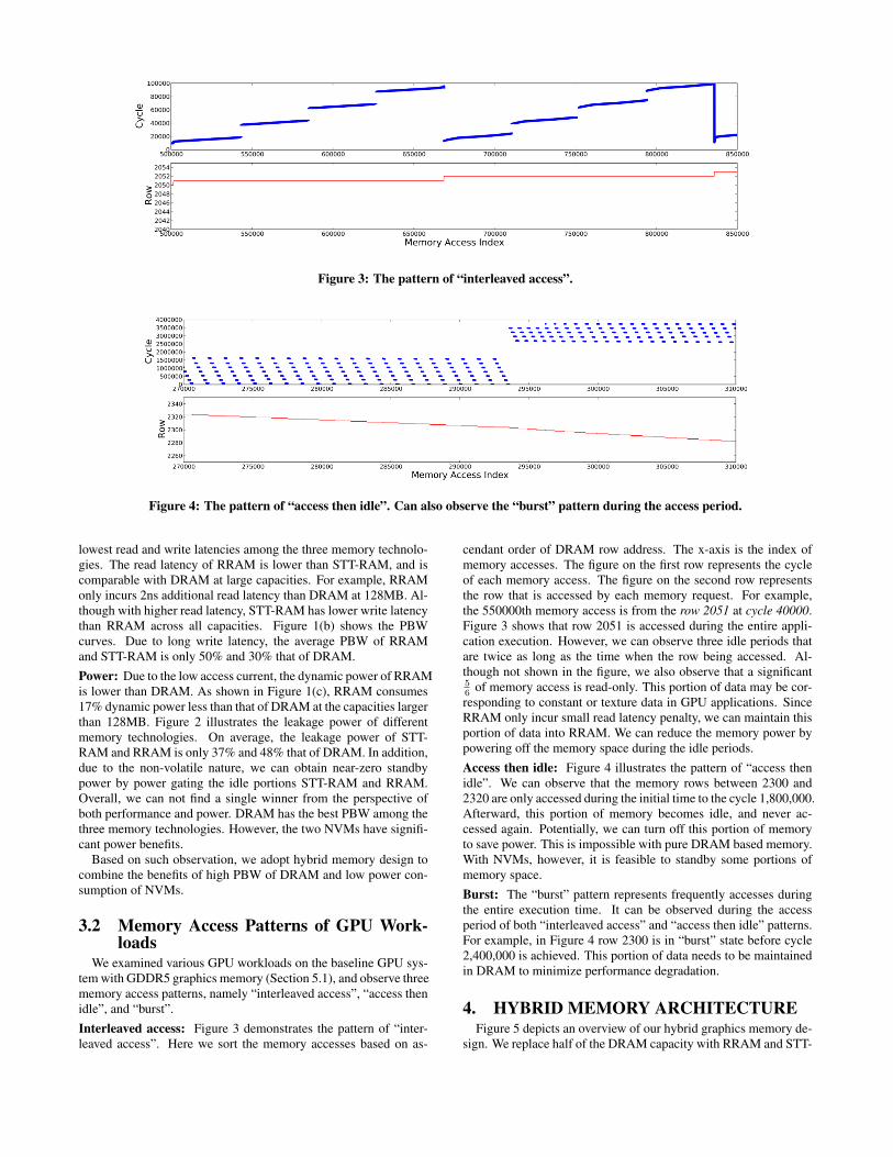
Figure 3: The pattern of “interleaved access”.
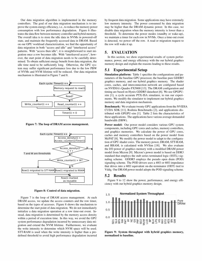
Figure 4: The pattern of “access then idle”. Can also observe the “burst” pattern during the access period.
lowest read and write latencies among the three memory technolo-gies. The read latency of RRAM is lower than STT-RAM, and iscomparable with DRAM at large capacities. For example, RRAMonly incurs 2ns additional read latency than DRAM at 128MB. Al-though with higher read latency, STT-RAM has lower write latencythan RRAM across all capacities. Figure 1(b) shows the PBWcurves. Due to long write latency, the average PBW of RRAMand STT-RAM is only 50% and 30% that of DRAM.Power: Due to the low access current, the dynamic power of RRAMis lower than DRAM. As shown in Figure 1(c), RRAM consumes17% dynamic power less than that of DRAM at the capacities largerthan 128MB. Figure 2 illustrates the leakage power of differentmemory technologies. On average, the leakage power of STT-RAM and RRAM is only 37% and 48% that of DRAM. In addition,due to the non-volatile nature, we can obtain near-zero standbypower by power gating the idle portions STT-RAM and RRAM.Overall, we can not find a single winner from the perspective ofboth performance and power. DRAM has the best PBW among thethree memory technologies. However, the two NVMs have signifi-cant power benefits.
Based on such observation, we adopt hybrid memory design tocombine the benefits of high PBW of DRAM and low power con-sumption of NVMs.
3.2 Memory Access Patterns of GPU Work-loads
We examined various GPU workloads on the baseline GPU sys-tem with GDDR5 graphics memory (Section 5.1), and observe threememory access patterns, namely “interleaved access”, “access thenidle”, and “burst”.Interleaved access: Figure 3 demonstrates the pattern of “inter-leaved access”. Here we sort the memory accesses based on as-
cendant order of DRAM row address. The x-axis is the index ofmemory accesses. The figure on the first row represents the cycleof each memory access. The figure on the second row representsthe row that is accessed by each memory request. For example,the 550000th memory access is from the row 2051 at cycle 40000.Figure 3 shows that row 2051 is accessed during the entire appli-cation execution. However, we can observe three idle periods thatare twice as long as the time when the row being accessed. Al-though not shown in the figure, we also observe that a significant56
of memory access is read-only. This portion of data may be cor-responding to constant or texture data in GPU applications. SinceRRAM only incur small read latency penalty, we can maintain thisportion of data into RRAM. We can reduce the memory power bypowering off the memory space during the idle periods.Access then idle: Figure 4 illustrates the pattern of “access thenidle”. We can observe that the memory rows between 2300 and2320 are only accessed during the initial time to the cycle 1,800,000.Afterward, this portion of memory becomes idle, and never ac-cessed again. Potentially, we can turn off this portion of memoryto save power. This is impossible with pure DRAM based memory.With NVMs, however, it is feasible to standby some portions ofmemory space.Burst: The “burst” pattern represents frequently accesses duringthe entire execution time. It can be observed during the accessperiod of both “interleaved access” and “access then idle” patterns.For example, in Figure 4 row 2300 is in “burst” state before cycle2,400,000 is achieved. This portion of data needs to be maintainedin DRAM to minimize performance degradation.
4. HYBRID MEMORY ARCHITECTUREFigure 5 depicts an overview of our hybrid graphics memory de-
sign. We replace half of the DRAM capacity with RRAM and STT-

Figure 5: Overview of GPU system with hybrid memory. (a) Conventional GPU system with off-chip GDDRs. (b) GPU system withhybrid memory.
RAM. With half the capacity, DRAM can provide up to 25% highermemory bandwidth by scaling up the clock frequency. We migratethe read-only and infrequently accessed data to NVMs. Due tothe non-volatility, we can significantly reduce the memory powerconsumption by powering off the idle NVM space. The hardwaremodification is limited to the memory interface and controllers andno modification is required to the internal structures of the GPUprocessors and the memory arrays.
4.1 Hardware ConfigurationPartitions of different memory technologies: Our hybrid graph-ics memory consists of DRAM, RRAM, and STT-RAM partitions.Frequently accessed data is maintained in the DRAM that has thehighest PBW among the three memory technologies. The two NVMpartitions are used to store the data with low access frequency. Theidle rows in the NVM partitions are powered off. Between the twoNVMs, RRAM is used to store data that is read-only or with ex-tremely low write intensity. Since STT-RAM has better write per-formance than RRAM, it is used to store the infrequently accesseddata with higher write intensity.Capacity of each partition: Our baseline GPU system (Section 5.1)employs 256MB DRAM per channel. In our hybrid graphics mem-ory, we reduce the DRAM capacity to 128MB per channel andreplace the rest 128MB with RRAM. This is based on the obser-vation that the dynamic power of DRAM is higher than RRAM atthe capacities of higher than 128MB. In addition to power bene-fits, reducing the DRAM capacity can also improve PBW. In Fig-ure 1(b), we observe that the PBW of DRAM at 128MB is 1.25×that of 256MB. We adopt 8MB STT-RAM per channel. This isbased on the fact that the dynamic power of STT-RAM is the low-est among the three memory technologies at small capacities. Therow buffer size of different memory partitions are configured to be256-bit, so that data migration incurs minimum overhead in addressmapping. The hybrid memory may incur a small increased area(9mm2) compared to the baseline (45nm technology). However,the increased memory area is only limited to the off-chip memoryand we do not expect high cost increase to the GPU system.
Memory interface: Figure 6 shows our memory interface configu-ration. As shown in Figure 6, an additional bus of 32 bits is adoptedto accommodate data migration and NVM reads (data will be readout directly from the NVMs, once it is migrated to the NVM par-titions). GPU can read and write from the DRAM partition. GPU
can only read from the NVM partition. In our experiments, we con-sider the additional I/O termination power incurred by this modifi-cation and show the total system power is still reduced with suchI/O overhead. Furthermore, multiplexing is required to switch thereads between DRAM and NVMs.
Memory controller: A NVM controller is integrated in the mem-ory controller to accommodate the data migration and manage thepower mode of NVMs. Components of the NVM controller includedata migration buffers, read buffers, and registers to store the mem-ory idle states. We modify the memory controller to facilitate datamigration. Timers are employed to manage the idle state of eachDRAM row. Each row also has counters to collect memory accessdata. We evaluated the area and power overhead of these timersand counters. For 32-bit timers (counters), the total storage sizewill be 32.3KB (assume 2KB page size (row-buffer size) as sameas the baseline GDDR5). This is negligible in a memory system of256MB. An address mapping table is used to store the new addressafter a row is migrated from DRAM to NVMs.
4.2 Data Migration Mechanism
Figure 6: Memory interface configuration and data flow be-tween memory controller and hybrid memory.
Our data migration algorithm is implemented in the memorycontrollers. The goal of our data migration mechanism is to im-prove the system energy efficiency, i.e., to reduce the memory powerconsumption with low performance degradation. Figure 6 illus-trates the data flow between memory controller and hybrid memory.The overall idea is to store the idle data in NVMs in powered-offstate, and maintain the frequently accessed data in DRAM. Basedon our GPU workload characterization, we find the opportunity ofdata migration in both “access and idle” and “interleaved access”patterns. With “access then idle”, it is straightforward to start mi-gration once a row becomes idle. With “interleaved access”, how-ever, the start point of data migration needs to be carefully deter-mined. To obtain sufficient energy benefit from data migration, theidle time need to be sufficiently long. Otherwise, the GPU sys-tem may suffer significant performance loss due to the low PBWof NVMs and NVM lifetime will be reduced. Our data migrationmechanism is illustrated in Figure 7 and 8.
Figure 7: The loop of DRAM access management.
Figure 8: Control of data migration.
Figure 7 is the loop of DRAM access management. At eachDRAM access, we update the access counters and the row timer,based on the types of accesses. Figure 8 shows the mechanism todetermine the start point of data migration. We do not immediatelyinitialize a data migration operation at a row time-out event. In-stead, data migration is determined by the memory access densitywithin a period of execution time. In this way, we avoid the GPUsystem performance degradation incurred by unnecessary data mi-gration and extend the NVM lifetime. Furthermore, we evaluatethe write intensity to determine which NVM space will be used.STT-RAM is used when the write intensity is higher than a pre-defined threshold to avoid high performance degradation incurred
by frequent data migration. Some applications may have extremelylow memory intensity. The power consumed by data migrationmay be higher than the DRAM dynamic power. In this case, wedisable data migration when the memory intensity is lower than athreshold. To determine the power modes (standby or wake-up),we maintain a timer for each row in NVMs. Once a time-out eventis detected, we power off the row. A read or migration request tothe row will wake it up.
5. EVALUATIONIn this section, we show experimental results of system perfor-
mance, power, and energy efficiency with the our hybrid graphicsmemory design and explain the reasons leading to these results.
5.1 Experimental SetupSimulation platform: Table 1 specifies the configurations and pa-rameters of the baseline GPU processor, the baseline pure GDDR5graphics memory, and our hybrid graphics memory. The shadercores, caches, and interconnection network are configured basedon NVIDIA’s Quadro FX5800 [13]. The DRAM configuration andtiming are based on Hynix GDDR5 datasheet [6]. We use GPGPU-sim [1], a cycle accurate PTX-ISA simulator, to run our experi-ments. We modify the simulator to implement our hybrid graphicsmemory and data migration mechanism.Benchmark: We evaluate twenty GPU applications from the NVIDIACUDA SDK [11], Rodinia Benchmarks [2], and applications dis-tributed with GPGPU-sim [1]. Table 2 lists the characteristics ofthese applications. The applications have various average demandedbandwidth (DBW).Power model: Our power model considers various GPU systemcomponents, including GPU cores and caches, memory controllers,and graphics memories. We calculate the power of GPU cores,caches and memory controllers based on the power model fromMcPAT [8]. We modify the power model to adapt to the configura-tion of GPU shader cores. The memory power, DRAM, STT-RAM,and RRAM, is calculated with NVSim [18]. We also evaluatethe I/O power of graphics memory with a modified DRAM powermodel from Micron [9]. Micron’s power model is based on DDR3standard that employs the stub series terminated logic (SSTL) sig-naling scheme. GDDR5 employs the pseudo open drain (POD)signaling scheme. The POD drivers uses a 40Ω or 60Ω impedancethat drives into a 60Ω equivalent on-die-terminator (ODT) tied toVddq. Our DRAM power model adopts the POD signaling scheme.
5.2 ResultsFigure 9 to 12 show the power, performance, and energy effi-
ciency with our hybrid graphics memory design.
SD1
SLA
BFS
NW
FWT PF NE
GS
PRF
SD2
MUM
LUD BP BLK
LPS
HS
RAY
STO
AES
BN GM
0.0
0.5
1.0
1.5 Normalized System Throughput
PureDRAM
Figure 9: System throughput with hybrid graphics memory,normalized to baseline.
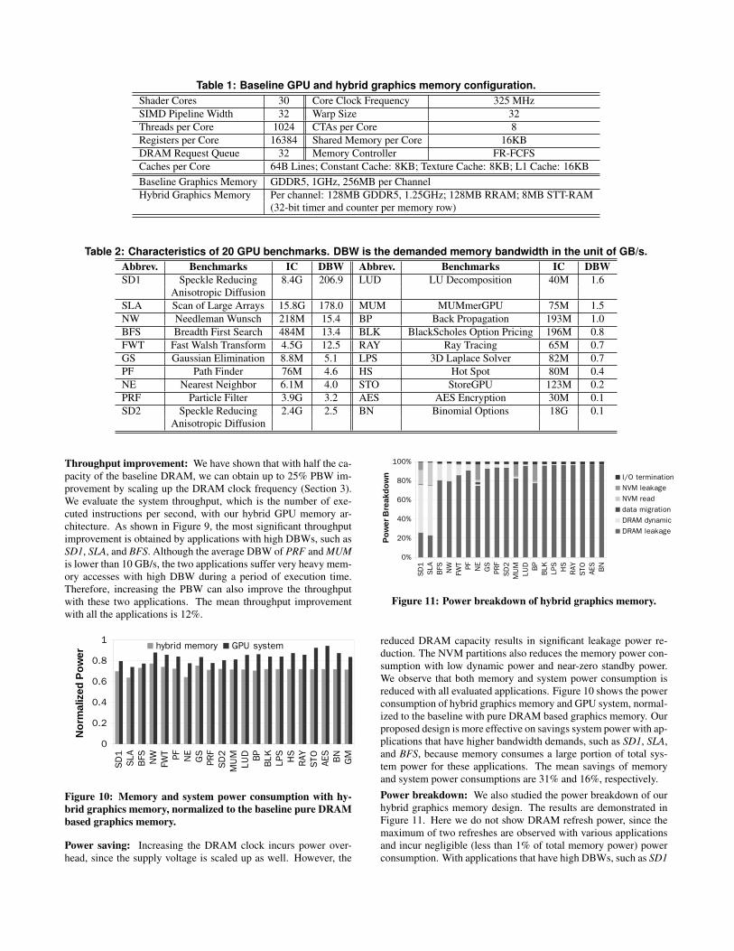
Table 1: Baseline GPU and hybrid graphics memory configuration.Shader Cores 30 Core Clock Frequency 325 MHzSIMD Pipeline Width 32 Warp Size 32Threads per Core 1024 CTAs per Core 8Registers per Core 16384 Shared Memory per Core 16KBDRAM Request Queue 32 Memory Controller FR-FCFSCaches per Core 64B Lines; Constant Cache: 8KB; Texture Cache: 8KB; L1 Cache: 16KBBaseline Graphics Memory GDDR5, 1GHz, 256MB per ChannelHybrid Graphics Memory Per channel: 128MB GDDR5, 1.25GHz; 128MB RRAM; 8MB STT-RAM
(32-bit timer and counter per memory row)
Table 2: Characteristics of 20 GPU benchmarks. DBW is the demanded memory bandwidth in the unit of GB/s.Abbrev. Benchmarks IC DBW Abbrev. Benchmarks IC DBWSD1 Speckle Reducing 8.4G 206.9 LUD LU Decomposition 40M 1.6
Anisotropic DiffusionSLA Scan of Large Arrays 15.8G 178.0 MUM MUMmerGPU 75M 1.5NW Needleman Wunsch 218M 15.4 BP Back Propagation 193M 1.0BFS Breadth First Search 484M 13.4 BLK BlackScholes Option Pricing 196M 0.8FWT Fast Walsh Transform 4.5G 12.5 RAY Ray Tracing 65M 0.7GS Gaussian Elimination 8.8M 5.1 LPS 3D Laplace Solver 82M 0.7PF Path Finder 76M 4.6 HS Hot Spot 80M 0.4NE Nearest Neighbor 6.1M 4.0 STO StoreGPU 123M 0.2PRF Particle Filter 3.9G 3.2 AES AES Encryption 30M 0.1SD2 Speckle Reducing 2.4G 2.5 BN Binomial Options 18G 0.1
Anisotropic Diffusion
Throughput improvement: We have shown that with half the ca-pacity of the baseline DRAM, we can obtain up to 25% PBW im-provement by scaling up the DRAM clock frequency (Section 3).We evaluate the system throughput, which is the number of exe-cuted instructions per second, with our hybrid GPU memory ar-chitecture. As shown in Figure 9, the most significant throughputimprovement is obtained by applications with high DBWs, such asSD1, SLA, and BFS. Although the average DBW of PRF and MUMis lower than 10 GB/s, the two applications suffer very heavy mem-ory accesses with high DBW during a period of execution time.Therefore, increasing the PBW can also improve the throughputwith these two applications. The mean throughput improvementwith all the applications is 12%.
SD1
SLA
BFS
NW
FWT PF NE
GS
PRF
SD2
MU
MLU
D BP BLK
LPS
HS
RAY
STO
AES
BN GM
0
0.2
0.4
0.6
0.8
1 hybrid memory GPU system
No
rma
lize
d P
ow
er
Figure 10: Memory and system power consumption with hy-brid graphics memory, normalized to the baseline pure DRAMbased graphics memory.
Power saving: Increasing the DRAM clock incurs power over-head, since the supply voltage is scaled up as well. However, the
SD1
SLA
BFS
NW
FWT PF NE
GS
PRF
SD2
MU
MLU
D BP BLK
LPS
HS
RAY
STO
AES
BN
0%
20%
40%
60%
80%
100%
I/O terminationNVM leakageNVM readdata migrationDRAM dynamicDRAM leakage
Po
we
r B
rea
kd
ow
n
Figure 11: Power breakdown of hybrid graphics memory.
reduced DRAM capacity results in significant leakage power re-duction. The NVM partitions also reduces the memory power con-sumption with low dynamic power and near-zero standby power.We observe that both memory and system power consumption isreduced with all evaluated applications. Figure 10 shows the powerconsumption of hybrid graphics memory and GPU system, normal-ized to the baseline with pure DRAM based graphics memory. Ourproposed design is more effective on savings system power with ap-plications that have higher bandwidth demands, such as SD1, SLA,and BFS, because memory consumes a large portion of total sys-tem power for these applications. The mean savings of memoryand system power consumptions are 31% and 16%, respectively.Power breakdown: We also studied the power breakdown of ourhybrid graphics memory design. The results are demonstrated inFigure 11. Here we do not show DRAM refresh power, since themaximum of two refreshes are observed with various applicationsand incur negligible (less than 1% of total memory power) powerconsumption. With applications that have high DBWs, such as SD1

SD
1S
LAB
FS NW
FWT PF NE
GS
PRF
SD
2M
UM
LUD BP
BLK LPS
HS
RAY
STO
AES
BN
GM
0.0
0.4
0.8
1.2
1.6
Normalized System Energy Efficiency
PureDRAM
Figure 12: System energy efficiency with hybrid graphics mem-ory, normalized to baseline.
and SLA, the dynamic power covers a significant portion of totalmemory power consumption due to the high memory access inten-sity of these workloads. In contrast, DRAM leakage power dom-inates the total memory power consumption of applications withlow DBWs, such as STO, AES, and BN. In this case, we cannotafford the dynamic power consumption of data migration and it istherefore disabled with these three applications to avoid the poweroverhead incurred by data migration.Energy efficiency: Figure 12 illustrates the results of system en-ergy efficiency, defined as the executed instructions per second perWatt. The system energy efficiency is improved with all the eval-uated applications. The most significant improvement can be ob-served with the applications having high DBWs. The mean im-provement of system energy efficiency is 33%.
6. CONCLUSION AND FUTURE WORKMemory bandwidth and power are the two critical resources of
GPU systems and significantly constrain the performance scaling.In this work, we propose a hybrid graphics memory that improvesboth memory bandwidth and system energy efficiency. The keyinsight in our work is that hybrid graphics memory design is espe-cially suitable for GPU applications. The memory access patternsof these applications are naturally used to hide the latency issue ofNVMs. Our initial results are very promising for future GPU sys-tems, improving 33% in system energy efficiency. Our migrationmechanism limits the frequency of write operations, and thereforewe do not expect significantly degradation of the lifetime.
Several directions can be explored in our future work. First ofall, this work only studies off-chip graphics memory. It may beinteresting to explore hybrid memory hierarchy design of the en-tire memory system with both on-chip caches, shared memories,and off-chip memories. Another interesting research direction isto improve the memory lifetime. In the hybrid graphics memory,the STT-RAM can be employed as the replacement of portions ofRRAM with error bits. How to balance between performance andpower of such design needs to be studied.
7. REFERENCES[1] A. Bakhoda, G. Yuan, W. Fung, H. Wong, and T. Aamodt.
Analyzing CUDA workloads using a detailed GPUsimulator. In Proc. of Intl. Symp. on Performance Analysis ofSystems and Software, pages 163–174, 2009.
[2] S. Che, M. Boyer, J. Meng, D. Tarjan, J. W. Sheaffer, S.-H.Lee, and K. Skadron. Rodinia: a benchmark suite forheterogeneous computing. In Proc. of Intl. Symp. onWorkload Characterization, pages 44–54, 2009.
[3] G. Dhiman, R. Ayoub, and T. Rosing. PDRAM: a hybridPRAM and DRAM main memory system. In Proceedings ofthe Design Automation Conference, pages 664–469, 2009.
[4] X. Dong, Y. Xie, N. Muralimanohar, and N. P. Jouppi.Hybrid checkpointing using emerging nonvolatile memoriesfor future exascale systems. ACM Trans. on Architecture andCode Optimization, 8:1–29, 2011.
[5] Elpida. Introduction to GDDR5 SGRAM.http://www.elpida.com/pdfs/e1600e10.pdf.
[6] Hynix. GDDR5 SGRAM datasheet.http://www.hynix.com/products/graphics/.
[7] K.-H. Kim, S. Hyun Jo, S. Gaba, and W. Lu. Nanoscaleresistive memory with intrinsic diode characteristics andlong endurance. Applied Physics Letters, 96(5):1–3, 2010.
[8] S. Li, J. H. Ahn, R. D. Strong, J. B. Brockman, D. M.Tullsen, and N. P. Jouppi. McPAT: an integrated power, area,and timing modeling framework for multicore and manycorearchitectures. In Proc. of the Intl. Symp. onMicroarchitecture., 2009.
[9] Micron. System-power calculator,http://www.micron.com/products/dram/syscalc.html.
[10] J. C. Mogul, E. Argollo, M. Shah, and P. Faraboschi.Operating system support for NVM+DRAM hybrid mainmemory. In Proceedings of the Conference on Hot Topics inOperating Systems, pages 14–14, 2009.
[11] NVIDIA. CUDA SDK.http://www.nvidia.com/object/cudasdks.html.
[12] NVIDIA. GeForce GTX 480.http://www.nvidia.com/object/productgeforcegtx480us.html.
[13] NVIDIA. Quadro FX5800 spec.http://www.nvidia.com/object/productquadrofx5800us.html.
[14] S. Raoux, G. W. Burr, M. J. Breitwisch, C. T. Rettner, Y.-C.Chen, R. M. Shelby, M. Salinga, D. Krebs, S.-H. Chen, H.-L.Lung, and C. H. Lam. Phase-change random access memory:a scalable technology. IBM Journal of Research andDevelopment, 52:465–479, 2008.
[15] Samsung. Green memory solution.http://www.samsung.com/global/business/semiconductor.
[16] X. Wu, J. Li, L. Zhang, E. Speight, R. Rajamony, and Y. Xie.Hybrid cache architecture with disparate memorytechnologies. In Proc. of the International Symposium onComputer Architecture, pages 34–45, 2009.
[17] Y. Xie. Modeling, architecture, and applications foremerging non-volatile memory technologies. IEEEComputer Design and Test, 28:44–51, 2011.
[18] C. Xu, X. Dong, N. P. Jouppi, and Y. Xie. Designimplications of memristor-based RRAM cross-pointstructures. In Proceedings of the Design, Automation andTest in Europe Conference, pages 1–6, 2011.
[19] W.-K. S. Yu, R. Huang, S. Q. Xu, S.-E. Wang, E. Kan, andG. E. Suh. SRAM-DRAM hybrid memory with applicationsto efficient register files in fine-grained multi-threading. InProceeding of the International symposium on Computerarchitecture, pages 247–258, 2011.