Optical Communication Engineering - University of … · Optical Communication Engineering ......
245
Optical Communication Engineering Prof Derek Abbott Email: dabbott@eleceng.adelaide.edu.au Phone: (+61 8) 8303-5748 Room location: Innova 3.47
Transcript of Optical Communication Engineering - University of … · Optical Communication Engineering ......

Optical Communication Engineering Prof Derek Abbott Email: [email protected]
Phone: (+61 8) 8303-5748 Room location: Innova 3.47

How to pass this course: o Come to all lectures o Do all exercises
o Read the text book
o Work through text book examples
o Study an hour per day (on this subject)
o Focus and good study habits
o Do everything I say

High Distinction
Pass
Best study habits
Poorest studyhabits
Highest IQ
Lowest IQ
TThhee BBiigg SSeeccrreett

2
Outline
1. Introduction
2. Fundamentals of Optics and Lightware Prop-agation
3. Optical Waveguides
4. Light Sources
5. Light Detectors
6. Fibre Components
7. Modulation
8. System Design
Albert Ludwig
Albert Ludwig
Albert Ludwig
v

3
Introduction
A historical view:
1880 Bell’s Photophone
1900s Signal Lamps
1960s Lasers
1970s Low-loss Optical Fibres
1980s Analogue and Digital Communications
1990s Fibre Networks

4
The basic communications system (simplex):
TRANSMITTER RECEIVER
MessageOrigin
Modulator
CarrierSource
InputChannelCoupler
InformationChannel
OutputChannelCouple
Detector
SignalProcessing
MessageOutput

5
Message Origin
• Transducer (eg. microphone or video camera)
• Electrical Origin (eg. computer data)
• Some Combination of Signals
Modulator
• Two main functions
1. Converts message into correct format
2. Impresses the data onto the carrier
• Analogue or digital format

6
Carrier Source
• Laser Diode (LD) or Light Emitting Diode (LED) –
both small, lightweight and low power consumption.
• Ideally:
1. Single frequency of operation
2. High power output
• In practice these are not achieved, so
1. Spectral width =⇒ limited information capacity
2. Low power =⇒ limited path length
• Output power proportional to input current – infor-
mation contained in variation of optical power (In-
tensity Modulation)
• Operating frequency of LDs and LEDs comparable
with frequencies where fibres have low attenuation.

7
Input Channel Coupler
• Interface between light source and the information
channel
• Power lost due to transfer from light source to the
small fibre core
Information Channel
• Glass or plastic optical fibre
• Require:
1. low attenuation and large acceptance of light from
source
2. low distortion due to dispersion to maximize in-
formation rate
• Often a compromise between 1 and 2

8
Output Channel Coupler
• Delivers light from the fibre to the detector
• Usually efficient
Detector
• Converts modulated light power to an electrical sig-
nal
• Semiconductor photodiode
Signal Processor
• As for any other communication system - amplifica-
tion and filtering
• Aim for high SNR (analogue system) or low BER
(digital system)
Message Output
• As for any other communication system - provide
appropriate format for output message

9
Optical System Capacity
Bandwidth for:
telephone 4 kHz
AM broadcast 10 kHz
FM broadcast 200 kHz
commercial TV 6 MHz
Bit rate for:
telephone 64 kbps (8 bits×2×4000)
video 81 Mbps (9 bits×2×4.5×106)
Multiplexed systems available up to several Gbps.
10
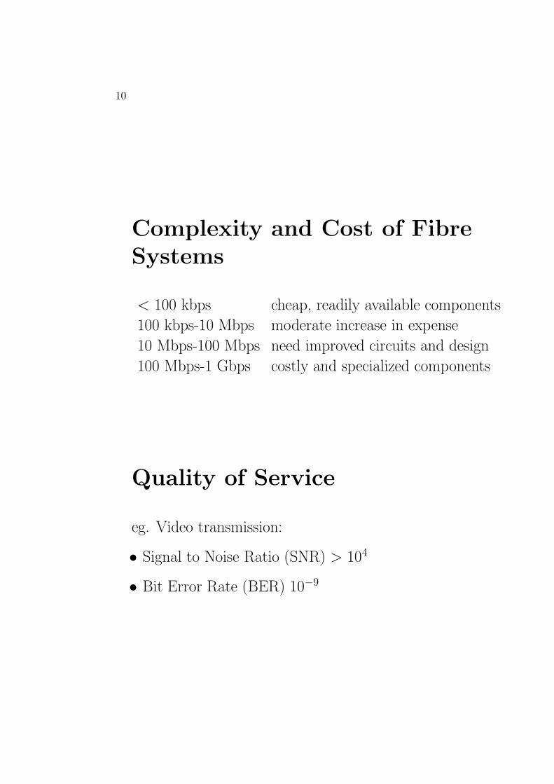
Complexity and Cost of FibreSystems
< 100 kbps cheap, readily available components
100 kbps-10 Mbps moderate increase in expense
10 Mbps-100 Mbps need improved circuits and design
100 Mbps-1 Gbps costly and specialized components
Quality of Service
eg. Video transmission:
• Signal to Noise Ratio (SNR) > 104
• Bit Error Rate (BER) 10−9

11
Optical Spectrum
Useful wavelengths for optical communications:
0.2-0.4 µm UV
0.4-0.7 µm Visible
0.7-2.0 µm IR
0.7-2.0 µm most widely used for fibre communications
since losses are low in windows within this region.

12
Wave Nature of Light
• Used in the analysis of propagation and guiding of
light
• Wavelength λ = v/f
• Wavelength of operation always quoted as a free-
space wavelength (ie. v = c)
Particle Nature of Light
• Used in the analysis of light generation by sources
• Photons, having energyWp = hf , where h is Planck’s
constant (6.626× 10⁻²⁴ Js)
13
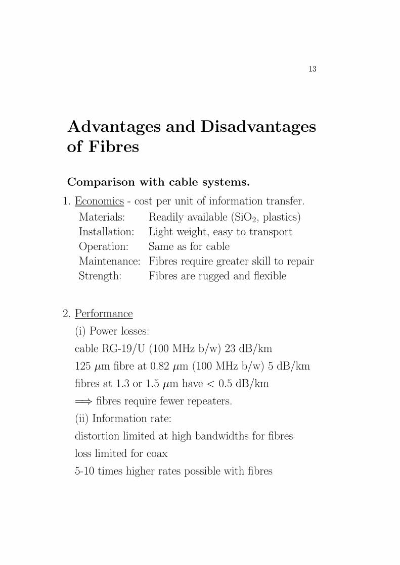
Advantages and Disadvantagesof Fibres
Comparison with cable systems.
1. Economics - cost per unit of information transfer.
Materials: Readily available (SiO2, plastics)
Installation: Light weight, easy to transport
Operation: Same as for cable
Maintenance: Fibres require greater skill to repair
Strength: Fibres are rugged and flexible
2. Performance
(i) Power losses:
cable RG-19/U (100 MHz b/w) 23 dB/km
125 µm fibre at 0.82 µm (100 MHz b/w) 5 dB/km
fibres at 1.3 or 1.5 µm have < 0.5 dB/km
=⇒ fibres require fewer repeaters.
(ii) Information rate:
distortion limited at high bandwidths for fibres
loss limited for coax
5-10 times higher rates possible with fibres
14
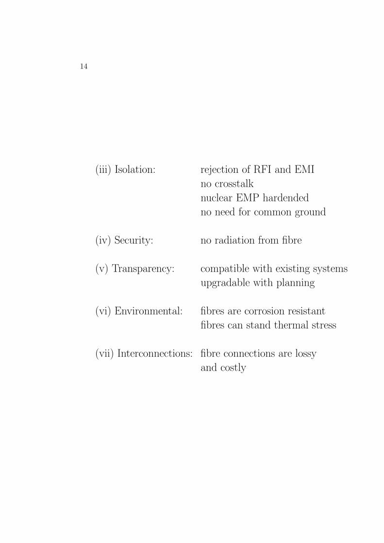
(iii) Isolation: rejection of RFI and EMI
no crosstalk
nuclear EMP hardended
no need for common ground
(iv) Security: no radiation from fibre
(v) Transparency: compatible with existing systems
upgradable with planning
(vi) Environmental: fibres are corrosion resistant
fibres can stand thermal stress
(vii) Interconnections: fibre connections are lossy
and costly

15
Applications of OpticalCommunications
• Telephone Links
1. trunk lines between exchanges
2. trans-oceanic links
3. fibre to the home
• Cable TV
• Remote monitoring
• Surveillance Systems
• Data Networks (eg. LANs)
• Military Command and Control
• Sensors (eg. fibre gyroscope, hydrophone etc.)

16
Review of Optics
Ray Theory
Rules for ray tracing based on Geomatric Optics (GO):
1. Velocity of ray v = c/n, where n is the index of
reflection of the media in which the ray travels.
2. Rays travel in straight paths unless deflected by a
change in the medium.
3. At a plane boundary, rays are reflected at an angle
θr equal to the angle of incidence θi, ie. θr = θi
4. Any power crossing the boundary is represented by
another ray whose direction θt is given by Snell’s
Law:sin θtsin θi
=n1
n2

17
Reference system for reflection and transmission at a
plane boundary:
Boundary
reflected
incident
transmitted
Note that ray theory cannot predict the intensity of
the reflected or transmitted rays.

18
Lenses
Can be used to focus light onto a fibre. Eg. a
cylindrical lens of diameter D and made from
material with refractive index n:
D
f
Fibre
Spherical faces defined by radii R1 and R2, and the
focal length is
1
f= (n− 1)
(1
R1+
1
R2
)

19
• The ratio f/D is defined as the f -number of the
lens.
• Large f-numbers are readily obtained.
• Small f-numbers require thick lenses, and often result
in spherical aberrations which blur the focus.
• Parallel off-axis rays are focussed in the focal plane
at a position determined by the central (undeflected)
ray.
• The lens can also be used to collimate a point source
located in the focal plane.

20
Ray tracing through lenses:
1. Rays travelling through the centre are undeviated.
2. Rays travelling parallel to the axis pass through the
focal point after emerging from the lens.
3. Incident rays parallel to a central ray intersect the
central ray in the focal plane after emerging from
the lens.
4. Incident rays passing through the focal point travel
parallel to the lens axis after emerging from the lens.
ff
4
231

21
Cylindrical Lenses
Useful for improving the symmetry of radiation from
line sources (eg. LED).
Planar sourceFocal line
Cylindricallens
Top View
Side View

22
Graded Index (GRIN) Rod Lens
• Dielectric rod (or fibre) having refractive index de-
creasing with radial distance from centre.
• Rays travel sinusoidal paths with one cycle being the
pitch, P .
• Quarter-wave pitch can be used as a lens with short
focal length.
• GRIN Rod, GRIN Rod Lenses and a fibre coupling
system shown below.
P
Grade Index Rod:
Quarter Pitch Lenses:
Collimating
Focussing
Application to fibre coupling:
lens
fibre

23
Imaging with Lenses
f f
di
O
I
do
Thin lens equation:
1
do+
1
di=
1
f
Magnification:
M =dido
=1
do/f − 1

24
Angular range:
f f
dido
1
M=
tanαi/2
tanαo/2
• Magnification M > 1 implies a decrease in beam
spreading.
• Fibres accept small cone angles whereas LEDs and
LDs radiate angles =⇒ can use a lens to improve
coupling.

25
Numerical Aperture
• Measure of the ability of an optical system to collect
light over a wide range of angles.
Consider the lens and detector system:
d
f
d
f
• Maximum acceptance angle θ
tan =d
2f(1)
• Define Numerical Aperture, NA as
NA = n0 sin θ (2)
where n0 is the refractive index of the medium be-
tween the lens and the detector.

26
Fibre Numerical Aperture
Fibre NA = sin θ
Fibre
• Typical glass fibres for high bandwidth have NA in
the range 0.1 to 0.3 =⇒1. difficult to couple to (sensitive to alignment)
2. low efficiency (rays outside acceptance angle θ)
• Plastic fibres may be lossy, but can be made with NA
in the range 0.4 to 0.5 to improve coupling efficiency
27
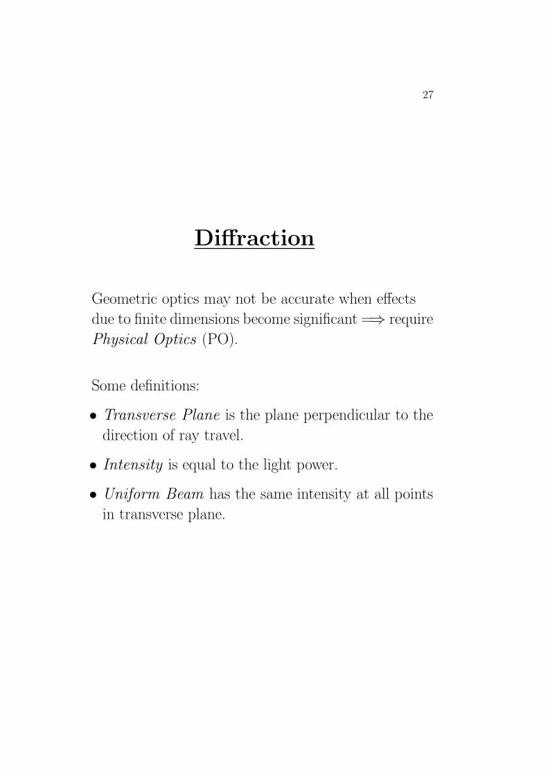
Diffraction
Geometric optics may not be accurate when effects
due to finite dimensions become significant =⇒ require
Physical Optics (PO).
Some definitions:
• Transverse Plane is the plane perpendicular to the
direction of ray travel.
• Intensity is equal to the light power.
• Uniform Beam has the same intensity at all points
in transverse plane.
28
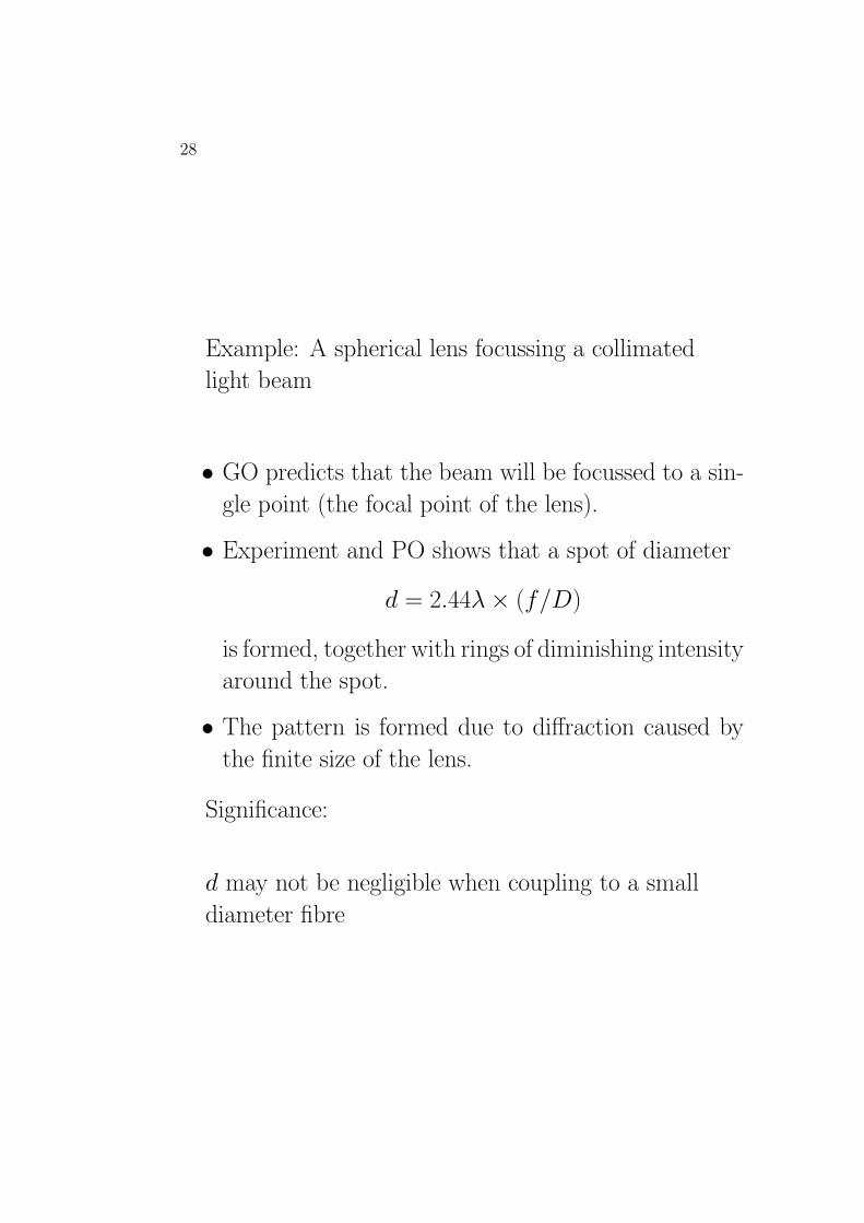
Example: A spherical lens focussing a collimated
light beam
• GO predicts that the beam will be focussed to a sin-
gle point (the focal point of the lens).
• Experiment and PO shows that a spot of diameter
d = 2.44λ× (f/D)
is formed, together with rings of diminishing intensity
around the spot.
• The pattern is formed due to diffraction caused by
the finite size of the lens.
Significance:
d may not be negligible when coupling to a small
diameter fibre

29
Gaussian Beams
A number of significant source (eg. gas lasers, some
LDs) radiate beams that have a Gaussian distribution
in the transverse plane.
.135
1
2w w w 2wr
I/I 0
where the intensity
I = I0e−2r2/w2
(3)
and w is the spot size - the radial distance at
which the intensity drop to I0/e2.
• Focussing a Gaussian beam with a lens yields a distri-
bution of light in the focal plane which is also Gaus-
sian:
I = I ′0e−2r2/w2
0
where the spot size in the focal plane is
w0 =λf
πw

30
Collimating a Gaussian Beam:
f
2w 2w0
z
• Close to the lens
I = I0e−2r2/w2
0
• At least distance from the lens, the beam diverges at
a constant angle θ radians, where
θ =2λ
πw
• The beam retains its Gaussian distribution, and at a
distance z has a spot size
w0 =λz
πw
• Small divergence angles are obtained when w λ.

31
Lightwave Fundamentals
Electromagnetic Waves
Light progates as waves of oscillating electric and
magnetic fields
E
z
t1 t3t2
t1 t3t2< <
where, for example, the electric field is described by
E = E0 sin(ωt− kz)
and
λ = wavelength
k =2π
λ=ω
v= propagation constant

32
• In free space, the notation λ0 and k0 are used. Note
that λ0/λ = n, hence wavelength in a dielectric
medium is shorter that in free-space.
• A plane wave has fields with the same phase over a
planar surface normal to the direction of propagation.
• The orientation in space of the electric field vector is
the polarization of the wave.
• A given distribution and polarization of fields is re-
ferred to as a mode.
• In optical fibres, many modes may exist and the wave
is said to be unpolarized.

33
• Attenuation due to energy loss is accounted for by
an attenuation constant α such that
E = E0e−αz sin(ωt− kz)
• Power (or intensity) is proportional to the square of
the field, so power loss (in dB) over length L is given
by
10 log(e−αL
)2
or power loss per meter is −8.685α where α is in
Np/m.

34
Dispersion
• Optical sojurce do not emit light at a single fre-
quency.
• Define
∆λ = line width or spectral width
∆f = optical bandwidth
which are related by
∆f
f=
∆λ
λ
• The smaller the line width, the more coherent is said
to be the source. Typical examples are as follows:
Soure ∆λ
LED 20-100 nm
LD 1-5 nm
NdYAG laser 0.1 nm
HeNe laser 0.002 nm

35
• Dispersion is the variation of wave velocity with
wavelength.
• Dispersion due to changes in the refractive index is
called Material dispersion.
• Dispersion due to the properties of the waveguide
modes in fibres is called waveguide dispersion.
• Dispersion due to modes having differing velocities is
called modal dispersion.
• All forms of dispersion have the same effect, and
cause pulse spreading in digital signals or amplitude
reduction in analogue signals.

36
Distortion due to pulse spreading in digital signals:
INPUT
time
optic
al p
ower
!#"%$&!OUTPUT
time
optic
al p
ower
'()*+,
Distortion due to amplitude reduction in analogue
signals:
INPUT
time
optic
al p
ower
-./012
OUTPUT
time
optic
al p
ower
345678

37
Analysis of Dispersion
Refractive Index Variation
9:
;<
=>
n 1.45
n’
n’’ 0
λ ≈ 1.3 µm for pure SiO2.

38
• Let τ be the time for a pulse to travel length L.
• τ/L will be function of wavelength for a dispersive
medium.
• Let λ1 and λ2 be the shortest and longest wave-
lengths of the pulse and hence:
∆λ = λ2 − λ1
∆(τ/L) = τ/L|λ2 − τ/L|λ1
where ∆(τ/L) is the pulse spread.
• Define the duration, ∆τ , of the pulse as the dura-
tion the instantaneous pulse power exceeds half
the peak power.
• From characteristics of τ/L it may be shown that
(τ/L)′ =∆(τ/L)
∆λ
= −λc
d2n
dλ2
= −λcn′′

39
• Define material dispersion, M , as
M =λn′′
c
usually in units of ps (delay) per nm (of spectral
width) per km (length).
• Pulse spread per unit length is therefore
∆(τ/L) = −M∆λ
where M > 0 implies that the shorter wavelengths
travel slower
• For SiO2, zero dispersion (M = 0) occurs around
λ0 = 1.3 µm. Doping with other materials may
change the zero dispersion point up to ±0.1 µm.
• Near the zero dispersion point pulse spreading can-
not be entirely neglected due to finite source spectral
width. For 1.2-1.6 µm, an approximate expression
for material dispersion is
M ≈ Mo
4
(λ− λ4
o
λ3
)
where Mo = −0.095 ps/(nm2×km)
40
Information Rate
• Pulse spreading limits the information rate.
• Consider a modulation frequency f = 1/T , where T
is the period.
• Source radiates between optical wavelengths λ1 and
λ2.
• Maximum allowable pulse spreading occurs when the
signals at λ1 and λ2 are time shifted so that they
cancel, ie.
∆τ =T
2and hence the modulation frequency is limited to
f <1
2∆τ
• Wavelengths between λ1 and λ2 do not cancel. The
limiting modulation frequency defined above is ap-
proximately the 3 dB optical bandwidth.
• The frequency-length limit is thus
f3dB × L =1
2∆(τ/L)

41
• For a Gaussian response, the actual analytic result is
f3dB × L =0.44
∆(τ/L)
• The total electrical loss for propagation along a path
may be written as La + Lf , where
La = loss due to attenuation and scattering
= loss due to pulse spreading
= −10 log e−0.693(f/f3dB)2
from which it can be determined that the loss f is
1.5 dB at a frequency corresponding to 0.707f3dB.
• THE OPTICAL 1.5 dB BANDWIDTH = THE ELEC-
TRICAL 3 dB BANDWIDTH
• The electrical frequency-length limit is therefore
f3dB(elec.)× L =0.35
∆(τ/L)

42
Consider a return-to-zero (RZ) digital signal:
z
T
1 1 0 1
timepo
wer
1/T 2/T
freq.
with a data rate RRZ = 1/T bps.
• The limit on the data rate imposed by the 3 dB dis-
persion limited bandwidth is
RRZ = f3dB(elec.) =0.35
∆τ
• Rate-length limit is therefore
RRZ × L =0.35
∆(τ/L)
• The allowable pulse spread is therefore 70% of the
pulse duration (or 35% of the time slot) to prevent
intersymbol interference.

43
Consider a non-return-to-zero (RZ) digital signal:
z
T
1 1 0 1
time
pow
er1/2T 1/T
freq.
with a data rate RNRZ = 1/T bps.
• The limit on the data rate imposed by the 3 dB dis-
persion limited bandwidth is
RNRZ = 2f3dB(elec.) =0.7
∆τ
• Rate-length limit is therefore
RNRZ × L =0.7
∆(τ/L)
• The allowable pulse spread is again 70% of the pulse
duration (here 70% of the time slot).

44
Information Capacity Examples
Limited by material dispersion in SiO2.
Source λ ∆λ M ∆(τ/L)
(µm) (nm) (ps/nm/km) (ns/km)
(i) LED 0.82 20 110 2.2
(ii) LED 1.5 50 (-)15 0.75
(iii) LD 0.82 1 110 0.11
(iv) LD 1.5 1 (-)15 0.015
OPTIC ELECTRICAL
f3dB × L RNRZ × L f3dB × L RRZ × L(GHz×km) (Gbps×km) (GHz×km) (Gbps×km)
(i) 0.23 0.32 0.16 0.16
(ii) 0.67 0.94 0.47 0.47
(iii) 4.55 6.4 3.2 3.2
(iv) 33.33 46.7 23.3 23.3

45
Resonant CavitiesFound in the construction of lasers: eg. the Fabry
Perot resonator below.Mirrors
Output
Amplifying Medium
A standing wave pattern set up between two mirrors:
L
• The cavity will support a longitudinal mode if
L =mλ
2where m is an integer
• The cavity resonants at
λ =2L
mand if the medium between the mirrors has a refrac-
tive index n, at a resonant frequency
f =mc
2nL

46
• Each value of m corresponds to a different longitudi-
nal mode.
• Spacing between adjacent modes is given by
∆fc =c
2Ln
• The corresponding separation in free-space wavelength
is
∆λc =λ2
0
c∆fc
where λ0 is the mean free-space wavelength.

47
Reflection at Plane Boundaries
Key reflecting surfaces in fibres include:
1. Input (air-glass) and output (glass-air) coupling.
2. Interface between fibre core and cladding.
3. Glass-air-glass boundary at fibre junctions.
• Reflection coefficient at a boundary between two
media for normal incidence is
ρ =n1 − n2
n1 + n2
where n1 is the media from which the wave is inci-
dent.
• A negative value of ρ indicates a 180 degree phase
shift of the reflected wave.
• Reflectance is the ratio of reflected to incident beam
intensity : ie. R = |ρ|2.

48
Fresnel’s Laws of Reflection
Parallel Polarization
?@ABCDEF GIH Et
Er
Ei
ρ|| =−n2
2 cos θi + n1
√n2
2 − n21 sin2 θi
n22 cos θi + n1
√n2
2 − n21 sin2 θi
Perpendicular Polarization
JLKMLNOLPQSR TVU
Et
Er
Ei
ρ⊥ =n1 cos θi −
√n2
2 − n21 sin2 θi
n1 cos θi +√n2
2 − n21 sin2 θi

49
• Note that the analysis only applies for specular re-
flection from perfectly smooth surfaces.
• Analysis does not apply to diffuse reflection from
rough surfaces.
• Zero reflection only occurs for parallel polarization at
the Brewster angle θB satisfied by
tan θB =n2
n1
• A quarter-wave antireflection coating may be used
to reduce reflections. From a quarter-wave layer with
refractive index n2, the normal incidence reflectance
is
R =
(n1n3 − n2
2
n1n3 + n22
)2
for which R = 0 when the layer has n2 =√n1n3.
50
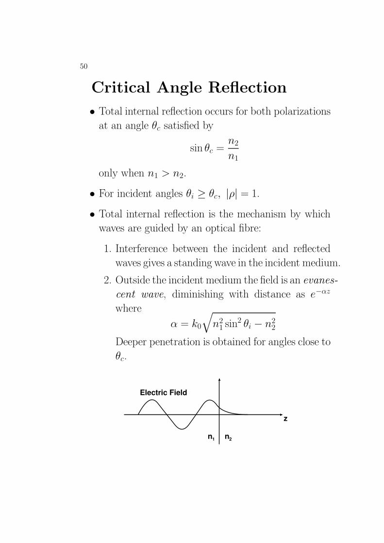
Critical Angle Reflection
• Total internal reflection occurs for both polarizations
at an angle θc satisfied by
sin θc =n2
n1
only when n1 > n2.
• For incident angles θi ≥ θc, |ρ| = 1.
• Total internal reflection is the mechanism by which
waves are guided by an optical fibre:
1. Interference between the incident and reflected
waves gives a standing wave in the incident medium.
2. Outside the incident medium the field is an evanes-
cent wave, diminishing with distance as e−αz
where
α = k0
√n2
1 sin2 θi − n22
Deeper penetration is obtained for angles close to
θc.
z
Electric Field
n2n1
51
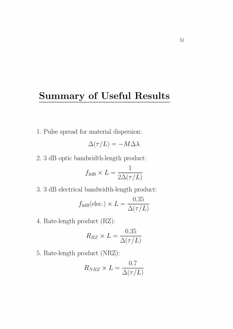
Summary of Useful Results
1. Pulse spread for material dispersion:
∆(τ/L) = −M∆λ
2. 3 dB optic bandwidth-length product:
f3dB × L =1
2∆(τ/L)
3. 3 dB electrical bandwidth-length product:
f3dB(elec.)× L =0.35
∆(τ/L)
4. Rate-length product (RZ):
RRZ × L =0.35
∆(τ/L)
5. Rate-length product (NRZ):
RNRZ × L =0.7
∆(τ/L)

52
6. Longitudinal mode separation in cavity:
∆fc =c
2Ln
7. Reflectance for normal incidence:
R =
(n1 − n2
n1 + n2
)2
8. Critical angle for total reflection:
sin θc =n2
n1

53
Optical Waveguides
1. Dielectric Slab Waveguide
y
x
z W Xn2
n1
n3
• For a ray to propagate in the central film n3 < n1
and n2 < n1.
• Smooth boundaries required for specular reflection.
• Suitable integrated optic material have low losses:
eg. Lithium Niobate (LiNbO3) 1 dB/cm and Gallium
Arsenide (GaAs) 2.2 dB/cm.
54
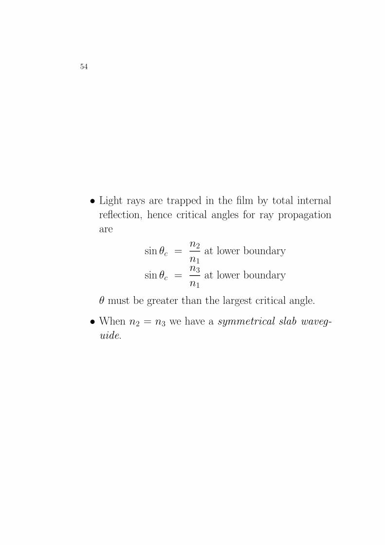
• Light rays are trapped in the film by total internal
reflection, hence critical angles for ray propagation
are
sin θc =n2
n1at lower boundary
sin θc =n3
n1at lower boundary
θ must be greater than the largest critical angle.
• When n2 = n3 we have a symmetrical slab waveg-
uide.

55
• The total field is the sum of two plane waves - one
travelling upward at angle θ and one travelling down-
ward at angle θ, both with a propagation constant
k = k0n1:
YZh hk
[
\Upward wave Downward wave
• The longitudinal propagation constant β along the
direction of wave propagation (z-direction) is
β = k sin θ = k0n1 sin θ
• Standing wave set up in the transverse direction (y-
direction), so the electric field for even modes (sym-
metrical about y = 0) is
E = E1 coshy sin(ωt− βz)
and for odd modes (asymmetrical about y = 0) is
E = E1 sinhy sin(ωt− βz)
where E1 is the peak value of the electric field and
h = k cos θ is the vertical component of k.

56
• The phase velocity is given by
vp =ω
β
• We define an effective refractive index neff as
neff =c
vp=β
k0= n1 sin θ
which plays the same role as n does in unguided
wave propagation. Hence in the waveguide, the wave-
length in the direction of propagation is
λg =λ0
neff
• Outside the film the fields decay with an attenuation
factor
α = k0
√n2
1 sin2 θ − n22
so the fields outside the film are
E = E2e−α(y−d/2) sin(ωt− βz) for y > d/2
E = E2e−α(y+d/2) sin(ωt− βz) for y < −d/2
for symmetrical slab waveguide.

57
Modes in Symmetrical Slab Waveguide
• Total internal reflection occurs for rays between the
critical angle θ = θc and θ = 90.
• At θ = 90, neff = n1, and at θ = θc, neff = n2, so
n2 ≤ neff ≤ n1
• Only certain ray directions, however, are permitted.
Each allowed direction corresponds to a mode.
• The condition for a particular mode is that the phase
shift ∆φ for a round trip as shown below must satisfy
∆φ = 2πm
where m is an integer.
] ^
• ∆φ is the sum of the phase shift along the path and
the phase shift due to the reflections.
• Waves that do not satisfy the condition on ∆φ will
attenuate rapidly due to destructive interference (ie.
they are evanescent.)

58
Transverse Electric (TE) Modes
• Waves polarized in the x-direction (perpendicular
polarization) give rise to TE modes
_E
• Solution to the round trip phase condition yields for
even symmetry in the transverse plane
tanhd
2=
1
n1 cos θ
√n2
1 sin2 θ − n22
• and for odd symmetry in the transverse plane
cothd
2=
1
n1 cos θ
√n2
1 sin2 θ − n22
where h = k cos θ = 2πn1λ0
cos θ.

59
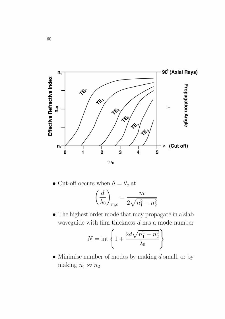
Construction of mode charts:
For trapped rays in the range θc ≤ θ ≤ 90 determine
the lowest order soultion:
1. Choose θ
2. Determine neff = n1 sin θ
3. Solve for the lowest order solution of hd
4. Obtain (d
λ0
)
0
=hd
2πn1 cos θ
Higher order solution for TEm modes are noted from
the periodic nature of the tan and cot functions, and
are found from(d
λ0
)
m
=
(d
λ0
)
0
+m
2n1 cos θ
60
TE 0
TE 1
TE 2
TE 3
TE 4
TE 5
n1
n eff
n2
Eff
ectiv
e R
efra
ctiv
e In
dex
0 1 2 3 4 5
90o (Axial Rays)
`
acb
Propagation A
ngle
(Cut off)
dfehgji
• Cut-off occurs when θ = θc at(d
λ0
)
m,c
=m
2√n2
1 − n22
• The highest order mode that may propagate in a slab
waveguide with film thickness d has a mode number
N = int
1 +
2d√n2
1 − n22
λ0
• Minimise number of modes by making d small, or by
making n1 ≈ n2.

61
Transverse Mode Patterns
n2n1n2
TE0
TE1
TE2
ie. the mode index refers to the number of nulls in
the transverse electric field pattern.

62
Transverse Magnetic (TM) Modes
• Wave having parallel polarization give rise to TM
modes.
kE
• Solution to round trip phase condition yields for even
symmetry
tanhd
2=
n1
n22 cos θ
√n2
1 sin2 θ − n21
and for odd symmetry
cothd
2=
n1
n22 cos θ
√n2
1 sin2 θ − n21
• If n1 ≈ n2 then the mode chart is nearly the same
for TE modes.
• Cut-off values for TEm and TMm modes are the same
even if n1 6= n2.
• TM0 and TE0 modes have no cut-off, therefore a sin-
gle mode film cannot be obtained since discontinu-
ities may depolarize the wave.

63
Asymmetric Dielectric Slab Waveguide
• Occur when n2 6= n3, and are used in Optoelectronic
Integrated Circuits (OEICs).
• An example of an asymmetric slab waveguide is a
thin ZnS film (n1 = 2.29) on a glass substrate (n2 =
1.5). Here n3 = 1 (ie. air).
• Rays must exceed the larger of the two critical angles
to avoid leakage into the substrate and consequent
losses.
• TE and TM modes exist, but are no longer degener-
ate even for n1 ≈ n2.
• All modes, including the TE0 and TM0 modes, have
a non-zero cut-off condition.
• Transverse field distributions are asymmetrical.

64
Edge Coupling to Slab Waveguide
• Used here to demonstrate the potential difficulties
and inefficiencies.
• For practical purpose, prism coupling is commonly
used.
1. Numerical Aperture Considerations
ln0
mon p qn2
n2
n1
• From Snell’s law:
n0 sinα0 = n1 sinα1
= n1 cos θ

65
• If α0 is large, θ may drop below θc and the wave will
not propagate along the film.
• α0 is called the waveguide acceptance angle.
• At θ = θc
sin θ =n2
n1and hence
cos θ =
√n2
1 − n22
n1
giving a numerical aperture
NA = n0 sinα0 =√n2
1 − n22
• We define a fractional refrective index change as
∆ =n2 − n1
n1
which for n2 ≈ n1 yields
NA = n1
√2∆

66
The consequences:
For thin films, where only a few modes are supported:
• Propagation angles of different modes are widely spaced.
• Incident rays must match these angles for efficient
coupling.
For thick films, where many modes propagate:
• Propagation angles of different modes are closely spaced
in the range between θc and 90.
• All incident rays are captured within the acceptance
angle.

67
Other coupling considerations:
• Radiation modes: Untrapped rays do not reflect
100% of the light, but may still give rise to a wave
which attenuates along the length of the film as the
energy is transmitted across the boundaries.
• Cladding modes: Critical angle reflections may oc-
cur at the outside boundaries:
n0
n2
n2
n1
n0

68
Radiation from the end of the film:
• For thick films: the film will radiate over the accep-
tance angle.
• For thin films: the film will radiate according to the
distribution of each mode as determined by diffrac-
tion theory.
Note that a large acceptance angle implies the need
for large ∆, which in turn suggests that many modes
must be propagating.

69
Other losses:
• Reflection losses : Light is reflected from the end of
the film due to the change in refractive index. Antire-
flection coatings may be used to improve efficiency.
• Alignment losses : A lens can be used to focus light
onto the film if the numerical aperture of the source
and the film are mismatched.
• Mode mismatch losses : The transverse distribution
of the incident wave from the source must match that
of the mode in order to couple to it. This is especially
true if its is desired to couple to a single mode. (eg.
Gas laser radiation matches the TE0 mode distribu-
tion, whereas LED radiation is less well ordered.)
70
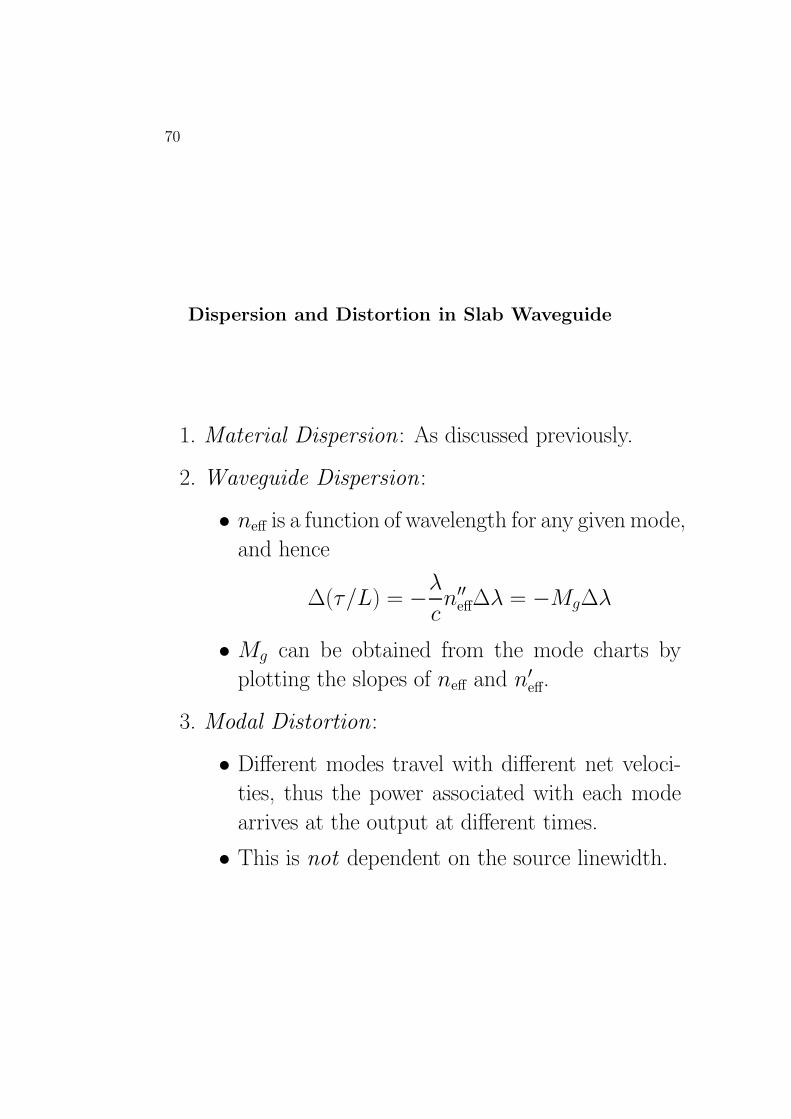
Dispersion and Distortion in Slab Waveguide
1. Material Dispersion : As discussed previously.
2. Waveguide Dispersion :
• neff is a function of wavelength for any given mode,
and hence
∆(τ/L) = −λcn′′eff∆λ = −Mg∆λ
• Mg can be obtained from the mode charts by
plotting the slopes of neff and n′eff.
3. Modal Distortion :
• Different modes travel with different net veloci-
ties, thus the power associated with each mode
arrives at the output at different times.
• This is not dependent on the source linewidth.

71
Modal Distortion
• Determine the time of travel for the axial ray:
ta =L
cn1
and for the ray at the critical angle (distance travelled
= Ln1/n2, velocity = c/n1):
tc =L
cn2n2
1
so we have
∆(τ/L) =n1(n1 − n2)
cn2
=n1∆
c
=NA2
2cn1
Note that all three mechanisms exist simultaneously
for multimode propagation.

72
Optical Fibres
Step Index (SI) Fibres
n2
n1
a
z core
cladding
n
Refractive index of core is n1 and of the cladding is
n2, where n1 > n2.
• Critical angle for trapped rays in the core is given by
sin θc =n2
n1
• Fractional refractive index change is
∆ =n2 − n1
n1

73
Features of the cladding:
• Light still travels in the caldding, but decays rapidly
away from the interface.
• The cladding should be non-absorbing.
• The cladding assists the support and handling of the
fibre.
• The cladding protects the core.
• Cladding modes are possible, but usually attenuate
rapidly away from the excitation. Buffer layers are
sometimes used eliminate cladding modes.
Fibre sizes (denoted core-size/cladding-size diameter
in µm):
common size 50/125, 100/140, 200/230.
74
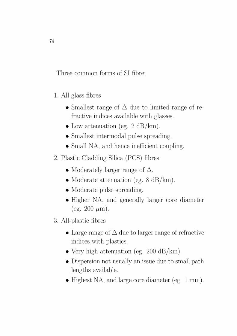
Three common forms of SI fibre:
1. All glass fibres
• Smallest range of ∆ due to limited range of re-
fractive indices available with glasses.
• Low attenuation (eg. 2 dB/km).
• Smallest intermodal pulse spreading.
• Small NA, and hence inefficient coupling.
2. Plastic Cladding Silica (PCS) fibres
• Moderately larger range of ∆.
• Moderate attenuation (eg. 8 dB/km).
• Moderate pulse spreading.
• Higher NA, and generally larger core diameter
(eg. 200 µm).
3. All-plastic fibres
• Large range of ∆ due to larger range of refractive
indices with plastics.
• Very high attenuation (eg. 200 dB/km).
• Dispersion not usually an issue due to small path
lengths available.
• Highest NA, and large core diameter (eg. 1 mm).

75
Modes in SI Fibres
Plot a Mode Chart in terms of normalized frequency
V =2πa
λ0
√n2
1 − n22
where a is the core radius.
n1
n eff
n2
0 1 2 3 4 5 6V
HE11
TM01
TE01
HE21
EH11
HE12
HE31

76
• TE and TM modes exist.
• HE and EH are hybrid modes having both electric
and magnetic field components along the fibre axis.
• For a conventional SI fibre each curve of the mode
chart actually represents two orthogonal modes, both
travelling with the same velocity.
• Energy is easily coupled between the orthogonal modes
at discontinuities or inhomegeneities.
• Longitudinal propagation factor for a given mode is
found from
β = k0neff

77
• For large values of V , many modes will propagate
(multimode operation).
• The closer each mode is to cut-off, the deeper the
evanescent fields penetrate the cladding.
• For V > 10, the number of modes in all polarizations
is approximately
N =V 2
2
• Lowest order mode is the HE11 mode, having a Gaus-
sian transverse field pattern. For 1.2 < V < 2.4 the
spot size (or mode field radius) is given by
w
a= 0.65 + 1.619V −
32 + 2.879V −6

78
For Single Mode Operation in SI Fibre:
• A single mode will propagate if V < 2.405, and hence
a
λ0=
2.405
2π√n2
1 − n22
=2.405
2πNA
• Note that actually two orthogonal HE11 modes may
exist, travelling with the same velocity (ie. having
the same neff).
• A true single mode fibre can be obtained in a po-
larization preserving fibre which exhibits birefrin-
gence, where the effective refreactive index depends
on the polarization.
• Birefringence may be obtained by designing asym-
metries into the fibre as shown below.
elipticalcore
Borondoping
(a) (b)
• The mode polarization will depend on the polariza-
tion of the excitation.

79
Graded Index (GRIN) Fibre
n2 a
z core
cladding
nn(r)
n2 n1
• Index variation
n(r) =
n1
√1− 2(r/a)α∆ for r ≤ a
n1
√1− 2∆ = n2 for r > a
where
n1 = refractive index along fibre axis
n2 = refractive index of cladding
a = core radius
α = profile index
∆ =n2
1 − n22
2n21
≈ n1 − n2
n1for n1 ≈ n2

80
• Ray paths through GRIN fibre:
2a
escaping ray
• Acceptance angle and numerical aperture decrease
away from the fibre axis, since rays beyond the crit-
ical angle are not reflected at the outer boundary.
2a rtsouvtwox
Hence coupling efficiency is lower than SI fibres with
comparable core radius and ∆.

81
• A Parabolic Profile (α = 2) is commonly used:
n(r) = n1
√1− 2(r/a)2∆ for r ≤ a
which for ∆ 1 becomes
n(r) =
n1
[1− (r/a)2∆
]for r ≤ a
n1(1−∆) for r > a
• Numerical aperture of parabolic profile GRIN fibre
is
NA =√n(r)2 − n2
2
= n1(2∆)12
√1− (r/a)2
which, on-axis, is noted to be the same as for a SI
fibre.
82
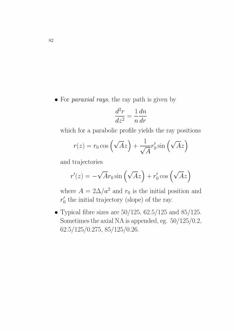
• For paraxial rays, the ray path is given by
d2r
dz2=
1
n
dn
dr
which for a parabolic profile yields the ray positions
r(z) = r0 cos(√
Az)
+1√Ar′0 sin
(√Az)
and trajectories
r′(z) = −√Ar0 sin
(√Az)
+ r′0 cos(√
Az)
where A = 2∆/a2 and r0 is the initial position and
r′0 the initial trajectory (slope) of the ray.
• Typical fibre sizes are 50/125, 62.5/125 and 85/125.
Sometimes the axial NA is appended, eg. 50/125/0.2,
62.5/125/0.275, 85/125/0.26.

83
Modes in GRIN Fibres
• Explicit formula available for neff for a parabolic pro-
file:
neff =βpqk0
= n1 − (p + q + 1)
√2∆
k0a
• Lowest order mode is p = q = 0.
• Total number of modes in a multimode fibre is given
by
N =V 2
4ie. half the number found in a SI fibre for the same
V .
• Cut-off condition occurs when neff = n2. Approxi-
mate expression for single mode operation is
a
λ0<
1.4
π√n1(n1 − n2)
• Max. value of a/λ0 60% higher than for SI fibre.

84
Mode distributions for parabolic profile:
• Lowest order mode is circularly symmetrical and Gaus-
sian
E00 = E0e−α2r2/2 sin(ωt− β00z)
-2 0 2 yz
• Higher order modes not circularly symmetrical.
E10 = E1αxe−α2r2/2 sin(ωt− β00z)
0 |~-3 3
E20 = E2
[2(αx)2 − 1
]e−α
2r2/2 sin(ωt− β00z)
0 ~-3 3
85
Attenuation in Optical Fibres
Plastic fibres have high attenuation and are not used
for long distance communications.
Glass fibres are widely used for long distance
communications. Glasses are used with the following
properties:
• Formed by fusing molecules of Silica (SiO2).
• Product is a mixture having variations in molecular
locations (unlike a crystal).
• Glass may be doped with titanium, thallium, germa-
nium, boron etc. to vary the refractive index.
• High chemical purities are obtained.

86
1. Absorption Losses
(i) Intrinsic Absorption
• Natural property of the glass itself.
• Absorption due to electronic and molecular transi-
tion bands - has peak in UV and decreases with wave-
length.
• Absorption due to vibration of chemical bonds - has
peak in IR and increases with decreasing wavelength.
• Intrinsic losses are quite small in the wavelength re-
gion of interest.

87
(ii) Impurities
• Transition metals (Fe, Cu, V, Co, Ni, Mn, Cr) absorb
strongly in the wavelength region of interest.
• Transition metal atoms have complete inner shells.
The absorption of light elevates energy level to a
higher shell. Transition energy corresponds to pho-
ton energies in the useful region.
• OH ion has a stretching vibration resonance at 2.73
µm, with overtones at 1.37 µm, 1.23 µm and 0.95
µm when embedded in SiO2.
• OH impurities must be kept below 1 ppm by special
manufacturing precautions.

88
(iii) Atomic Defects
• Example: Titanium (Ti4+) dopant does not absorb,
but Ti3+ may be formed during fibrization, and in
this state absorbs heavily.
• Irradiation by X-rays, gamma-rays, neutrons etc. also
causes atomic defects – such defects are more signif-
icant at shorter wavelengths.
• Atomic defects also caused by contamination by met-
als (e.g. platinum from crucibles) during manufac-
ture.

89
2. Rayleigh Scattering
• Random molecular variations within the fibre are
caused when the glass cools after production.
• Concentration fluctuation also occur when fibre has
more than one oxide.
• These variations cause localized variations in the re-
fractive index, which are modelled as small (< wave-
length) scatterers embedded in an otherwise homo-
geneous medium.
• The scattering of photons in this manner is called
Rayleigh scattering:
and the loss is given by
L = 1.7
(0.85
λ0
)4
dB/km

90
• Rayleigh scattering is the fundamental limiting loss
for fibres.
• 1/λ4 variation suggests the need to work at longer
wavelength for lowest possible loss.
Inhomogeneities:
• Larger discontinuities can also cause scattering:
1. Discontinuities caused by a rough core-cladding
interface.
2. Material inhomogeneities on a large scale.

91
3. Geometric Effects
(i) Macroscopic Bending
• Bending a fibre onto a spool or around a corner:
R
at some radius R, the condition θ2 < θc is met, and
total internal reflection no longer occurs.
• Some light will leak from the bend.
• Higher order modes are most susceptible to loss at
bends.

92
(ii) Macroscopic Bending
• Local stresses casued by outer sheath protecting the
cable may cause small axial distortions randomly
along the fibre.
• Axial distortions cause losses as well as coupling be-
tween modes.

93
Total Attenuation
800 900 1000 1100 1200 1300 1400 1500 1600 17000
0.5
1.0
1.5
2.0
2.5
3.0
Wavelength (nm)
FirstWindow
TotalLoss
RayleighScattering
SecondWindow
OH AbsorptionPeak
ThirdWindow
Att
enat
ion
(dB
/km
)
Minimum loss in glass fibres occurs around 1.55 µm.

94
Total Attenuation
Optical Time Domain Reflectometry is often used
to measure attenuation.
• Access only needed at one end of the cable.
• Reflection from discontinuities can be localized, whereas
Rayleigh Scattering provides a continuous return.
Rayleigh Scattering
Fresnel Reflections
splice
Connector
End1 Distance End2
Opt
ical
Pow
er

95
Pulse Distortion and Information Rate
• A fibre link is said to be
– Power Limited : if the attenuation reduces the
signal level below that capable of reliable detec-
tion.
– Bandwidth Limited : if distortion precludes the
correct recovery of the signal at the receiver.
• The attenuation is the total of all the mechanisms
described above.
• The distortion is the total effect of
– Material Dispersion.
– Waveguide Dispersion.
– Modal Distortion.

96
Distortion in SI Fibres
• For multimode fibres, modal distortion (which is not
dependent on the source linewidth) is often the key
mechanism.
∆(τ/L)mod =n1
c∆ =
NA2
2cn1
• This gives an overestimate of the effect due to two
phenomena:
1. Mode Mixing.
2. Preferential Attenuation.

97
1. Mode Mixing:
• Energy is exchanged continuously between modes
along fibre.
• On average path travelled by each ray is nearly
the same.
• Mode mixing is not perfect, so multimode distor-
tion is still present.
• Also increases attenuation since some rays will be
deflected into paths at less than θc.
2. Preferential Attenuation:
• Higher order modes have longer path lengths and
higher attenuation.
• Contribution of higher order modes to pulse re-
construction is lower, and hence there is lower
distortion.
• Overall attenuation is higher if power is in higher
order modes.
• For short links, fewer higher order modes are ex-
cited.
98
Dispersion:
• Total dispersion is due to material dispersion (M)
and waveguide dispersion (Mg):
∆(τ/L)dis = −(M + Mg)∆λ
• Mg < M for short wavelengths.
• Mg significant in the range 1.2-1.6 µm where M is
smaller.
Total pulse spreading given by:
(∆τ )2 = (∆τ )2mod + (∆τ )2
dis

99
Distortion in Single Mode Fibres
• Only material and waveguide dispersion.
• Material dispersion most significant at short wave-
lengths (800-900 nm).
• Near 1.3 µm waveguide dispersion must be consid-
ered:
– just beyond zero matrial dispersion M < 0
– at this point Mg > 0
– the two phenomena can be used to counteract
one another.
• Long, high data-rate fibres can be constructed with
single mode operation.

100
• Since lowest attenuation occurs at 1.55 µm, meth-
ods to make dispersion small at this wavelength are
needed:
1. Dispersion shifted fibres have a triangular re-
fractive index profile to make M + Mg = 0 at
1.55 µm.
2. Dispersion flattened fibre have the core surrounded
first by a low refractive index layer to make M +
Mg small across a range of wavelengths.
0
1.2 1.3 1.4 1.5 1.6 1.7
Conventional
Dispersion Flattened
Dispersion Shifted
30
20
10
-10
-20
-30
Wavelength (um)
Dis
pers
ion
(ps/
nm/k
m)

101
Distortion in GRIN Fibres
• GRIN fibres have much lower modal distortion than
SI fibres, since non-axial rays passing through a lower
refracive index catch up with the axial rays. (α = 2
close to optimal.)
• Modal pulse spread per unit length given by
∆(τ/L) =n1∆2
2c
• Material and waveguide dispersion much the same as
for SI fibres.
102
Length Dependence of Pulse Spread
• For multimode fibres
– pulse broadening proportional to length over short
paths (< 1 km)
– over long paths pulses do not broaden as quickly.
• Over short lengths, mode mixing is incomplete.
• Over long paths an equilibrium is reached, the equi-
librium length Le being the transition between the
two conditions.
• Pulse spread can be written
∆τ = L∆(τ/L) for L ≤ Le
∆τ =√LLe∆(τ/L) for L > Le
• May be a trade off between a “poor” fibre encourag-
ing mode mixing but having high attenuation, and a
“good” fibre with lower attenuation but suppressing
mode mixing.

103
Connectors and Couplers
Sources of loss in fibre-to-fibre connections:
• Lateral Misalignment
Fibre CoreFibre Core ad
For multimode SI fibre:
L(dB) = −10 log
2
π
cos−1 d
2a− d
2a
√1−
(d
2a
)2
• Angular Misalignment
Fibre Core
Fibre Core
For multimode SI fibre:
L(dB) = −10 log
(1− n0θ
πNA
)

104
• Fibre Separation Loss
Fibre Core Fibre Core
x
Due to
– Reflections from the ends
– Acceptance angle limitation
L(dB) = −10 log
(1− xNA
4an0
)
NB. An index matching fluid may be used to decrease
fibre separation loss.
• Surface Roughness Loss
Fibre Core Fibre Core
Need to ensure that the ends are scribed and cut
smooth.
105
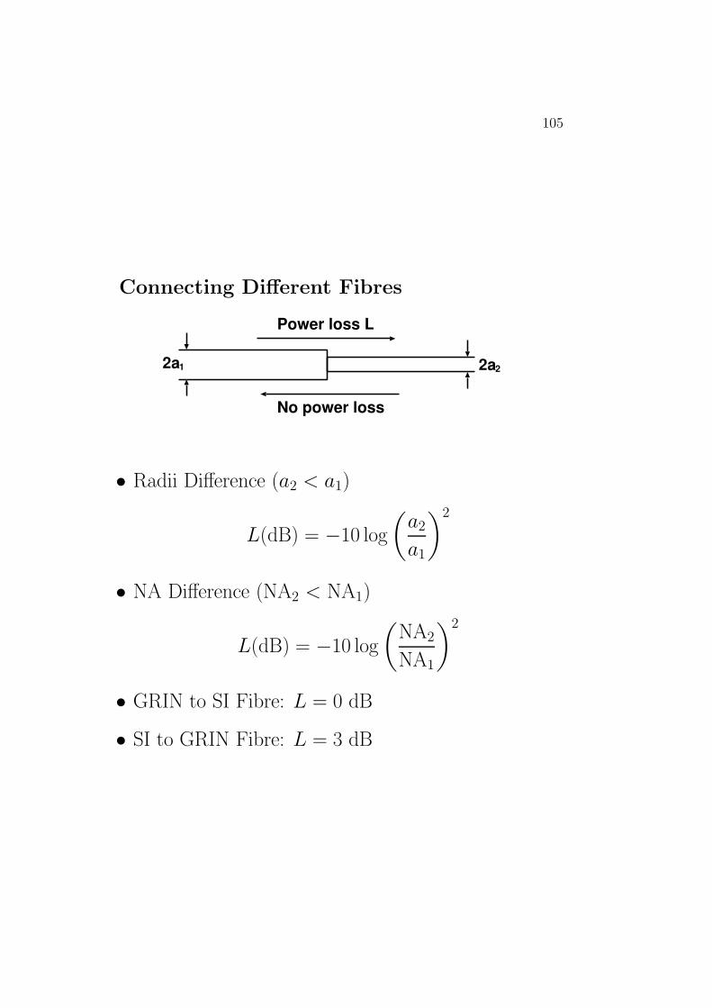
Connecting Different Fibres
2a1 2a2
Power loss L
No power loss
• Radii Difference (a2 < a1)
L(dB) = −10 log
(a2
a1
)2
• NA Difference (NA2 < NA1)
L(dB) = −10 log
(NA2
NA1
)2
• GRIN to SI Fibre: L = 0 dB
• SI to GRIN Fibre: L = 3 dB

106
Splices
• Fusion Splice – welding two fibres
• Adhesion Splice – bonding with epoxy
Connectors
• Low loss
• Repeatable
• Predictable
• Long life
• High strength
• Ease of assembly
• Ease of use
• Economical
• Compatible with environment
107
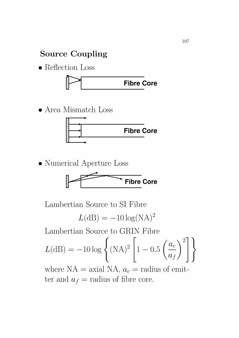
Source Coupling
• Reflection Loss
Fibre Core
• Area Mismatch Loss
Fibre Core
• Numerical Aperture Loss
Fibre Core
Lambertian Source to SI Fibre
L(dB) = −10 log(NA)2
Lambertian Source to GRIN Fibre
L(dB) = −10 log
(NA)2
[1− 0.5
(aeaf
)2]
where NA = axial NA, ae = radius of emit-ter and af = radius of fibre core.

108
Light Sources
Light Emitting Diodes
A pn semiconductor junction that emit light when
forward biased.
p n
Heavily DopedSemiconductor
I
V

109
ZERO BIAS
Conduction Band
Valence Band
WF
Wg
FORWARD BIASConduction Band
eVWF2
Valence Band
hfWF1
• When a free electron meets a free hole in the junction
region, they combine to give a photon.
• Radiation from a LED is caused by the recombina-
tion of holes and electrons injected into the junction
under forward bias conditions.

110
• The wavelength of operation is related to the bandgap
energy by
λ =hc
Wg
=1.24
Wg(eV )
• Bandgap energy (and hence operating wavelength)
varies depending on the proportion of the constituent
atoms:
Material λ (µm)
GaAs 0.9
AlGaAs 0.8-0.9
InGaAs 1.0-1.3
InGaAsP 0.9-1.7
• The homojunction LED described does not confine
the light well since
– charge carriers extend over large area
– after photons are created they diverge over unre-
stricted paths.
111
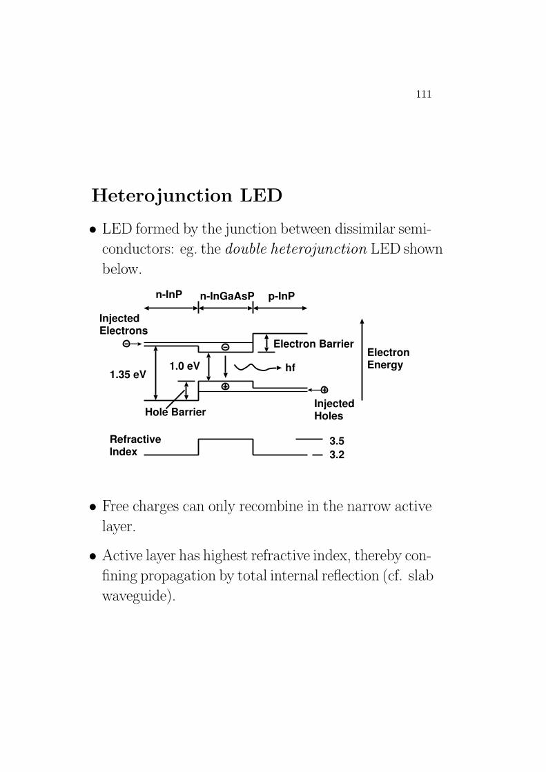
Heterojunction LED
• LED formed by the junction between dissimilar semi-
conductors: eg. the double heterojunction LED shown
below.
1.35 eVhf1.0 eV
InjectedElectrons
InjectedHoles
n-InP n-InGaAsP p-InP
Electron Barrier
Hole Barrier
ElectronEnergy
RefractiveIndex
3.53.2
• Free charges can only recombine in the narrow active
layer.
• Active layer has highest refractive index, thereby con-
fining propagation by total internal reflection (cf. slab
waveguide).

112
Surface emitting LED (Etched Well construction):
50 um
Metalisation
n-GaAs Substrate
n-AlGaAs Window
p-AlGaAs Active Layer
p-AlGaAs Confinement
p-AlGaAs Contact
InsulationSiO2
Metalisation
Epoxy
Fibre

113
Edge emitting LED:
Metalisation
Confinement
Active Layer
Confinement
Metalisation
Radiation

114
LED Characteristics
• The optical output power is (to a first approxima-
tion) proportional to the current i through the LED.
If N = i/e is the number of charge per unit time
available for recombination and η is the fraction of
charges that recombine to produce photons,
P = ηNWg Watts
= ηiWg(eV) eV/sec
• For digital modulation the LED is simply turned on
and off using current pulses (typically 50-100 mA).
• For analogue modulation a dc bias current is re-
quired to eliminate clipping of the output optical
power, so
i = Idc + ISP sinωt
P = Pdc + PSP sinωt

115
Bandwidth Considerations:
• For low modulation frequencies
PSP = a1ISP
where a1 = ∆P/∆i.
• For high modulation frequencies
– Junction and parasitic capacitances short circuit
the current, thereby reducing the optical power.
– Carrier lifetime τ is major limitation to high fre-
quency operation:
PSP =a1ISP√
1 + ω2τ 2
giving a 3 dB modulation bandwidth of
f3dB(elec.) =1
2πτ

116
• The rise time tr of a LED is defined as the time
taken for the optical power to rise from 10 to 90%
of its maximum in response to a step input current
(typically 5-200 ns). The electical bandwidth can be
obtained from
f3dB(elec.) =0.35
tr
(cf. an optical pulse having an impulse response of
width σ = 2tr.)
Spectral width:
• Carriers have energies distributed close to the Fermi
levels, and this distribution allows a range of photon
energies and hence wavelengths.
• Typical LED spectral widths are 20-50 nm for LEDs
operating in 800-900 nm range, and 50-100 nm for
LED operating in the longer wavelength regions.
117
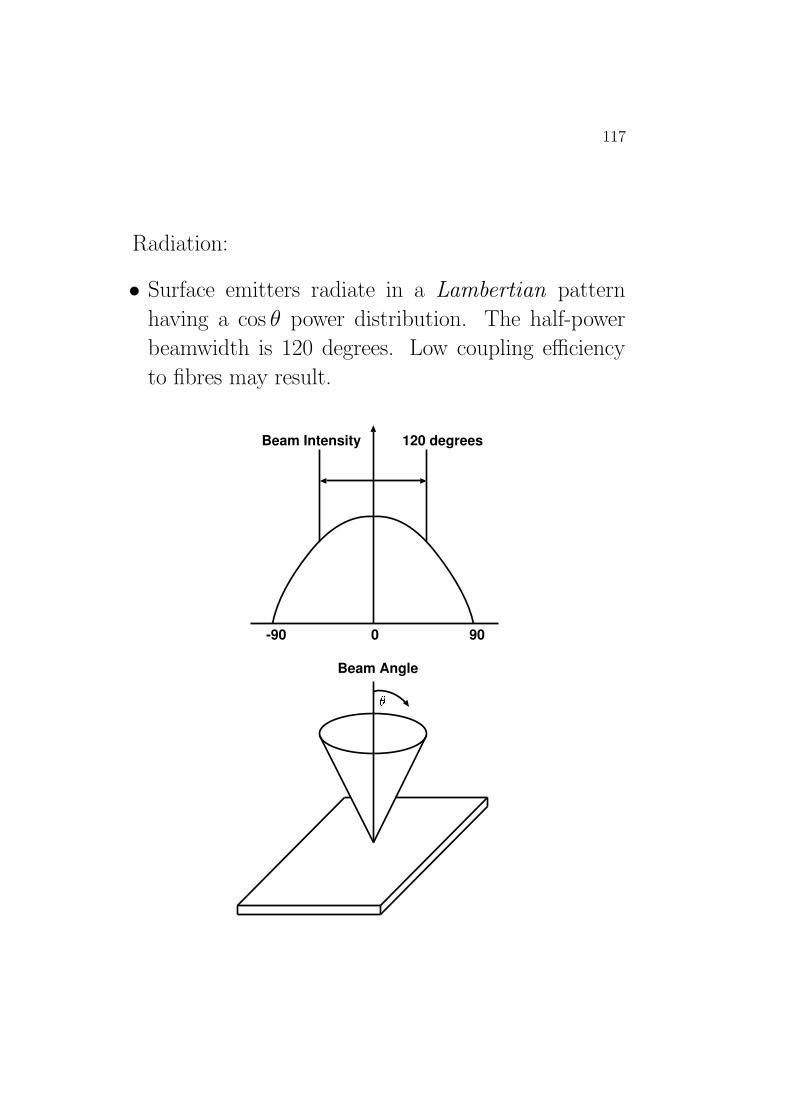
Radiation:
• Surface emitters radiate in a Lambertian pattern
having a cos θ power distribution. The half-power
beamwidth is 120 degrees. Low coupling efficiency
to fibres may result.
Beam Intensity 120 degrees
-90 0 90
Beam Angle

118
• Edge emitters radiate an asymmetrical power pattern
due to the beam confinement caused by the modes
in the slab waveguide forming the active region.
Beam Intensity
120 degrees
-90 0 90
Beam Angle
30 degreesParallelPlane
PerpendicularPlane

119
Lifetime and Operating Conditions:
• Lifetime of 105 hours are common if the LED is oper-
ated within its power, current and temperature lim-
its.
• Temperatures between -70 and 120 degrees Celcius
can be tolerated, although output power decreases
with increasing junction temperature.
Packages:
• Packages with glass covers are used.
• An external (or integral) lens can improve coupling
efficiency to a fibre.
• A pigtail construction allows a fibre to be bonded to
the chip during manufacture.

120
Lasers
1. Solid state (eg. Nd:YAG laser)
LEDs
MirrorNd:YAG Rod
PartialMirror
Output
• Fairly narrow linewidths available (eg. 0.1 nm)
• Costly and complex for use in communications sys-
tems.
• Requires an external modulator.

121
External Modulation:
• An external device is used to modulate the output
rather than modulating the input current.
• External modulators make use of electro-optic ma-
terial (eg. LiNbO3) – refractive index changes in
proportion to applied electric field.
• Eg. Mach-Zehnder Interferometer Modulator:
V O/PI/P
OpticalWaveguide
• Optical length of each path can be varied to effect
addition or cancellation of waves at the output.

122
2. HeNe Gas Laser
Mirror PartialMirror
OutputHeNe Gas
Power Supply
electrodes
L
• Operating wavelength λ0 = 633 nm.
• Linewidth ∆ = 0.002 nm.
• Used to test fibre systems for defects and to measure
NA.

123
Some terms used when considering lasers:
1. Pumping threshold : input power level above which
the laser will start to emit.
2. Output spectrum : optical frequency (wavelength)
response of the laser of the laser. Usually as series of
closely spaced peaks.
3. Radiation pattern : range of angles over which light
is emitted. Dependent on emitting area and modes
of oscillation.

124
Laser Operation
• Allowed energy levels for gas atoms are distinct lines
(cf. bands in semiconductors).
• Atoms usually in the ground state (lowest energy
level).
• Atoms absorb energy to rise to excited states.
– For Nd:YAG laser by absorbing an incoming pho-
ton.
– For HeNe laser by absorbing energy from ionized
electrons.
• The energy difference between two excited states of
the Ne atom corresponds to the 633 nm radiation
from HeNe laser.

125
• Various possibilities exist for photon interaction:
1. An incoming photon at 633 nm is absorbed, rais-
ing the Ne atom to the upper excited level.
2. A Ne atom in the upper excited level drops to the
lower level: ie. spontaneous photon emission.
3. A Ne atom in the upper level may be induced by
an incoming photon at 633 nm to emit another
photon and drop to the lower level: ie. stimu-
lated photon emission.
• If there are more Ne atoms in the lower level absorp-
tion of photons dominates.
• If there are more Ne atoms in the upper level (a
population inversion) then the number of photons
increases – giving rise to gain.

126
• For an oscillator we require:
– Amplification-provided by the medium.
– Frequency governing structure-provided by the
medium.
– Feedback-provided by the mirrors in a Fabry Perot
cavity configuration.
• Oscillations occurs when the gain exceeds all the
losses, including that due to output through the pae-
tial mirror.

127
• Finite linewidth occurs due to
– Thermal effects on energy levels.
– Doppler effect on sources in motion.
• Output spectrum is dependent on the linewidth and
the spacing between longitudinal cavity modes:
c2L
Cavity resonances
f
Gain of medium
• Output radiation pattern is dependent on the trans-
verse distribution of the modes in the cavity.
– Multimode beams tend to be large.
– Single mode beams have Gaussian distribution.

128
3. Laser Diodes
• Construction similar to edge emitting LED
Metalisation
GaAs Substrate
n-AlGaAs, W =1.8eV, Confinement
n-AlGaAs,
p-AlGaAs, p-GaAs Contact
InsulationSiO2
Metalisation
Emitting Edge
g
Wg =1.55eV, Active Layer
Wg =1.83eV, Confinement
Stripe Contact
1 um
0.2 um1 um
1 um
Operation:
• Forward bias junction to junction ro inject charges
giving spontaneous photon emission (low intensity).
• With high current density, stimulated emission oc-
curs and the optic gain is large.
• Threshold current reached when gain is large enough
to overcome losses −→ laser operation.

129
• High power with low threshold is achieved by confin-
ing injected charges and light using a heterojunction
structure.
• Laser cavity is formed by reflections from the ends
of the slab waveguide (ie. AlGaAs-air interface R =
0.32.)
• Several longitudinal modes may occur, together with
several transverse modes.
• Single transverse mdoe (HE11) operation may occur
for large currents – a Gaussian beam results.

130
Laser Diode Characteristics
• Typical threshold currents 50-200 mA, below which
the laser diode does not emit significantly.
• Typical output powers 1-10 mW (CW operation) for
20-40 mA drive current above threshold.
• DC bias needed for both digital and analogue mod-
ulation (due to threshold).
• Linearity of the output power/drive current function
dependent on operating point.
• Laser diodes are thermally sensitive:
– threshold varies with temperature.
– output power varies with temperature.
– wavelength varies with temperature.

131
• Laser diodes have shorter rise times than LEDs.
– Spontaneous emission lifetime, τsp, is the av-
erage time free carriers exist before recombining
spontaneously (as in LEDs).
– Stimulated emission lifetime, τst, is the aver-
age time free carriers exist before being forced to
recombine by stimulation.
– For a laser diode τst < τsp.
• Rise times of 0.1-1 ns are common, allowing internal
modulation up to several GHz.

132
• Linewidth of 1-5 nm are achievable. Linewidth is
often dependent on drive current, since at sufficiently
high current a single cavity mode can be excited.
• Radiation patterns of laser diodes differ from LEDs:
– laser diodes radiate asymmmetrically with smaller
cone angles than LEDs (hence potential for im-
proved fibre coupling).
– since the laser diode emission is more coherent
than the LED, the narrower pattern cut is due
to the wide aperture as expected from diffraction
theory.

133
4. Optical Amplifiers
Two general types:
1. Semiconductor Optical Amplifier : use the gain as-
sociated with semiconductor matrials (cf. laser oper-
ation).
2. Erbium Doped Fibre Amplifier (EDFA): use exter-
nal optical pumping source.
Erbium Doped Fibre Amplifiers:
W/M W/MInput
Erbium Doped Fibre
(1.55 um)
Laser DiodePump Source
(1.48 um)
(1.55 um)
(1.48 um)
Output

134
Operation:
• Erbium doped silica fibre has optical gain near 1.55 µm.
• Efficient pumping bands are 980 and 1480 nm.
• Couple input and pumping signals to Erbium doped
fibre by wavelength division multiplexing (eg. Prism
or reflection grating).
• Pumping light absorbed by Erbium atoms causing
population inversion.
• Stimulated emission by the signal photons then oc-
curs, increasing the signal power along the fibre.
• Any remaining pumping signal removed by wave-
length division demultiplexing.
• If pumping signal strength insufficient for complete
fibre length, absorption then ocurrs.
Characteristics:
• For 10 mW pumping power, 30 dB gain available
with about 3 dB noise figure over a 20 nm band.

135
Optical Detectors
Two photoelectric effects can be used:
• External photoelectric effect : electrons freed from
surface of a metal by energy absorbed from incident
photons. (eg. vacuum photodiode).
• Efficient pumping bands are 980 and 1480 nm.
• Internal photoelectric effect : free charge carriers
generated in semiconductor junction by incoming pho-
tons (eg. semiconductor photodiode).
Some terms that are used:
• Responsivity: ρ = iP
(A/w)
• Spectral response: responsivity as a function of wave-
length.
• Rise time: as for light sources (f3dB = 0.35tr
)

136
Vacuum Photodiode
Cathode(cesium)
1.9 eVemittedelectrons
i
RL
V
Anode
incomingphotons
Vb
• A single electron is liberated from the cathode if a
photon has
hf ≥ Φ
where Φ is the work function of the metal.
• f = Φ/h defines the lowest optical frequency that
can be detected, or in terms of wavelength
λ0(µm) =1.24
Φ(eV)

137
• Quantum efficiency is defined as
η =number of emitted electrons
number of incident photons
• Responsivity is therefore calculated as
– number of photons per second striking cathode
= P/(hf)
– number of emitted electrons per second = ηP/(hf)
– current i = ηP/(hf)× e– hence
ρ =i
P=ηe
hf=ηeλ
hc
• Output voltage v = ρPRL, ie. output voltage is
proportional to incident optic power.

138
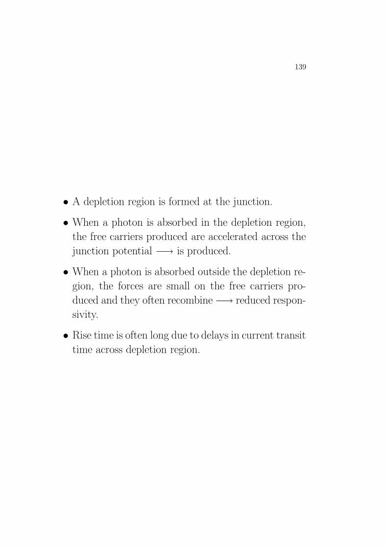
Semiconductor Photodiode
Formed by reverse biassing a pn-junction
hfi
RLVb
p nhf
Conduction Band
hf free electroncreated
free holecreated
depletion region
Valence Band
139
• A depletion region is formed at the junction.
• When a photon is absorbed in the depletion region,
the free carriers produced are accelerated across the
junction potential −→ is produced.
• When a photon is absorbed outside the depletion re-
gion, the forces are small on the free carriers pro-
duced and they often recombine−→ reduced respon-
sivity.
• Rise time is often long due to delays in current transit
time across depletion region.

140
PIN Photodiode
hfi
RLVb
p ni
V
• Solves problem of low responsivity and long rise time
by placing intrinsic semiconductor material (no dop-
ing) between the p and n region.
• High probability photons will be absorbed in the
large intrinsic region −→ high responsivity.
• Electrical forces strong across intrinsic region −→fast rise time.

141
An incoming photon must have an energy geater
than the material bandgap energy for electron-hole
pair creration, hence there is a cutoff wavelength
defined by
λ(µm) =1.24
Wg(eV)
Some material properties are:
η λ range Peak response Peak responsivity
µm µm (A/W)
Si 0.8 0.3-1.1 0.8 0.5
Ge 0.55 0.5-1.8 1.55 0.7
InGaAs 0.8 1.0-1.7 1.7 1.1
142
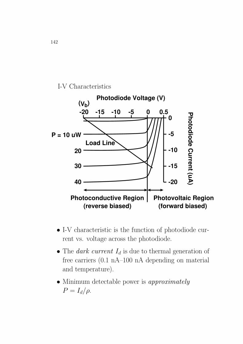
I-V Characteristics
-20 -15 -10 -5 0 0.50
-5
-10
-15
-20
Load LineP = 10 uW
20
30
40
Vb( )Photodiode Voltage (V)
Photoconductive Region(reverse biased)
Photovoltaic Region(forward biased)
Photodiode C
urrent (uA)
• I-V characteristic is the function of photodiode cur-
rent vs. voltage across the photodiode.
• The dark current Id is due to thermal generation of
free carriers (0.1 nA–100 nA depending on material
and temperature).
• Minimum detectable power is approximately
P = Id/ρ.

143
• Using the circuit below and the load line on the char-
acteristics we obtain
Vb + vd + RLid = 0
hf
RLVb V
+ -Vd
id
Hence can determine the output voltage for a given
optical input power
v = ρRLP
which is a linear relationship (until saturation is reached
at high optical powers).

144
Speed of response limited by
1. Carrier Transit Time:
• time for free charges to traverse the depletion re-
gion (approx. the width of the intrinsic layer for
PIN diodes).
• higher bias voltages reduce transit time.
• values of 1 ns or shorter are achievable.
2. Capacitance Effects:
RL VCdid
• Cd is the junction capacitance of the diode.
• Time constant isRLCd, giving a 10-90% rise time
of tr = 2.19CdRL, and a bandwidth of
f3dB =1
2πRLCd

145
Design trade-offs
• Design of diode: small junction area gives small ca-
pacitance and high bandwith, at the expense of re-
duced area for light capture.
• Choice of RL:
Eqn. Tradeoff
v = ρPRL RL large for large output voltage
Pmax = Vb/ρRL RL small for large dynamic range
f3dB = (2πRLCd)−1 RL small for large bandwidth
i2T = 4kT∆f/RL RL large to reduce thermal noise
current

146
I-V Converter:
• In previois circuit, voltage across diode decreases with
increasing optic power−→ nonlinearity as diode volt-
age drops to zero (ie. saturation).
• Without reducing RL we can use an I-V converter
circuit so vd = −Vb for all id (or optic powers).
Vb V
Rfid
• Output voltage v = −idRf .
147
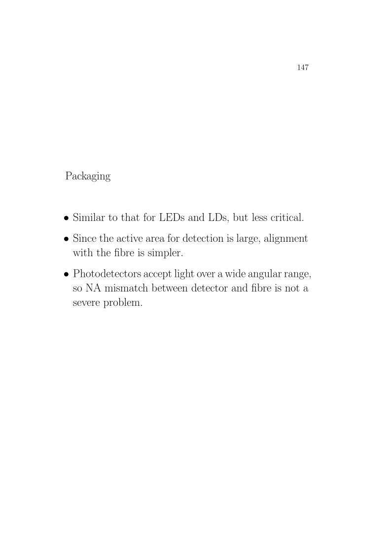
Packaging
• Similar to that for LEDs and LDs, but less critical.
• Since the active area for detection is large, alignment
with the fibre is simpler.
• Photodetectors accept light over a wide angular range,
so NA mismatch between detector and fibre is not a
severe problem.

148
Avalanche Photodiode
• Employ a multiplying effect to provide internal gain.
• Used when incident optic power is less than a few
microwatts.
• Avalanche effect multiplication:
– Photon absorbed in depletion region yielding a
free electron-hole pair.
– Large electrical force provided by reverse bias ac-
celerates the charges
– Charges collide with neutral atoms freeing addi-
tional electron-hole pairs
– These additional electron-hole pairs also acceler-
ate and collide to free further charges.

149
• A large reverse bias is needed to stimulate the avalanche
effect.
• Gain
M =1
1−(
vdVBR
)n
where n > 1 and VBR is the reverse breakdown volt-
age of the diode.
• The current generated is thus
i =MηeλP
hc
and responsivity is
ρ =Mηeλ
hc

150
• An example is the Reach Through Diode construc-
tion shown below.
hf
RLVb
i
V
p+ n+p
electron-holecreation
avalanchemultiplication
• Only the electrons created take part in the avalanche
effect to improve the noise characteristic of the de-
vice.

151
Modulation
Baseband Modulation
LED Modulation:
Baseband Analogue Techniques
• Photocurrent and optical power given by
i = Idc + ISP sinωt
P = Pdc + PSP sinωt
• Modulation factor is defined as
m′ =ISPIdc
and the optic modulation factor as
m =PSPPdc

152
• Recalling the bandwidth limitation on the LED due
to carrier life time τ
PSP =a1ISP√1 + ω2τ 2
we can relate the modulation factors by
m =m′√
1 + ω2τ 2
which for ωτ 1 gives a linear transfer function
with m ≈ m′.

153
• An example of an analogue modulation circuit for a
LED:
Vdc
CR1
Vin Rin R2 Re
(LED)

154
LED Nonlinearities:
• Nonlinearities in the system are due mostly to those
of the source.
• Model the optic power as
P = Pdc + a1is + a2i2s
where is is the signal current and Pdc is the constant
power produced by the bias current.
• If is = I sinωt then
P = Pdc +1
2a2I
2 + a1I sinωt +1
2a2I
2 cos 2ωt

155
• Define total harmonic distortion (THD) as
THD =electrical power in harmonics
electrical power in fundamental
=
(electrical power in harmonics
electrical power in fundamental
)2
and THD (dB) = -10log THD.
• For a signal is = I sinωt we have
THD =1
4
(a2I
a1
)2
• Typical THD is 30-60 dB for LEDs.

156
• If the signal has two frequency components such that
is = I1 sinω1t + I2 sinω2t then the optic power is
P = Pdc +1
2a2
(I2
1 + I22
)
+a1(I1 sinω1t + I2 sinω2t)
−1
2
(I2
1 cos 2ω1t + I22 cos 2ω2t
)
+a2I1I2cos(ω1 − ω2)t− cos(ω1 + ω2)t
• Note, the last term is called intermodulation dis-
tortion −→ coupling of power between channels is
possible.

157
Baseband Digital Modulation
• No dc bias current is needed for digital modulation.
• Distortion is not a significant effect since only on/off
states are detected.
• Example of a digital modulation circuit for a LED:
Vdc
C
R1
Vin
R
R2
(LED)

158
Laser Diode Modulation
• Design problems arise from:
– Existence of theshold current
– Age dependence of threshold
– Temperature dependence of threshold
– Temperature dependence of wavelength
• Digital systems are usually biassed near threshold
(Idc ≈ ITH).
• Analogue circuits require bias well above threshold
for linearity.
• Wavelength shifts may be important for multichannel
systems or systems operating near zero dispersion.
• Feedback control can be used to compensate for tem-
perature and age variations (but does not affect the
wavelength variantion problem).
159
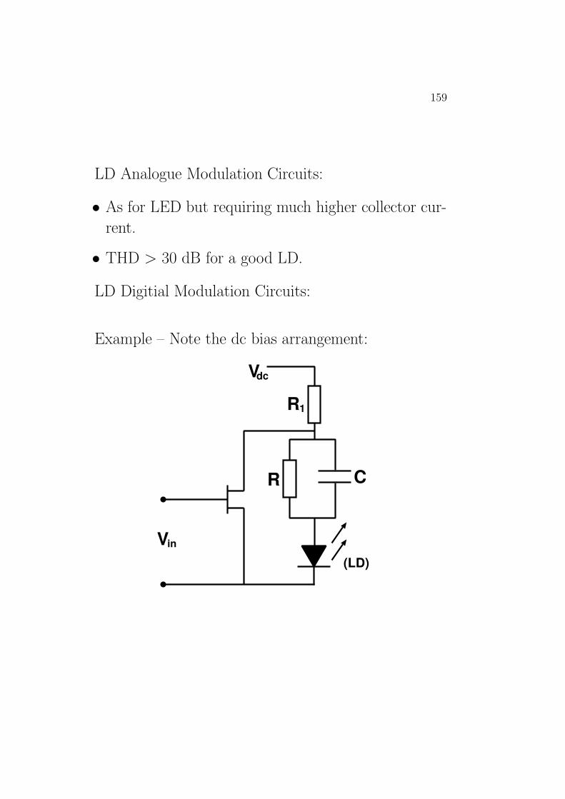
LD Analogue Modulation Circuits:
• As for LED but requiring much higher collector cur-
rent.
• THD > 30 dB for a good LD.
LD Digitial Modulation Circuits:
Example – Note the dc bias arrangement:
Vdc
C
R1
Vin
R
(LD)
160
Analogue Modulation Formats
• Notation:
i = I0 + Is cosωmt
P = P0 + Ps cosωmt
where ωm = 2πfm is the modulation frequency, I0
is the total dc current and P0 is the average optical
power.
1. AM/IM Subcarrier Modulation
• AM shifts the baseband to a different part of the
spectrum.
• Different channels can be received by filters tuned to
the appropriate subcarrier frequency.

161
• For a single sinusoidal modulation signal
i = I0 + Is(1 + m cosωmt) cosωsct
where ωsc = 2πfsc is the subcarrier frequency and
m ≤ 1. Hence the optic power is
P = P0 + Ps(1 + m cosωmt) cosωsct
• The spectrum of the AM signal is
SS ¡S¢
from which the bandwidth requirement B = 2fm is
obtained if fm is the highest modulating frequency.

162
Frequency Division Multiplex (FDM)
• Each channels has a different subcarrier frequency.
• Channels must be separated by more than 2ωm.
• Filters are used to separate channels.
• Nonlinearities create distortion and crosstalk between
channels.
• Total source power must be divided between the chan-
nels to prevent the peak drive current being exceeded.
• Used for cable TV because of the advantages:
– no additional conversion needed in modulation
format.
– smaller bandwidth than FM

163
2. FM/IM Subcarrier Modulation
• The modulating current is
i = I0 + Is cos[ωsct + θ(t)]
• If the modulating signal is a single sinusoid at fre-
quency fm = ωm/2π
i = I0 + Is cos[ωsct + β sinωt]
where β is the modulation index.
• If B is the basebandwith (= fm) and ∆f = βfm the
maximum frequency deviation, the total bandwidth
of the FM signal is
BT = 2B + 2∆f = 2fm(1 + β)

164
• The optic power is thus
P = P0 + Ps cos[ωsct + β sinωt]
• Since the information is extracted from the phase of
the subcarrier signal, effects of nonlinearities can be
minimised.
• FDM can be used with subcarrier frequencies sepa-
rated by at least BT .
• The FM format normally occupies a larger band-
width than the AM format.

165
Digital Modulation Formats
Why use digital anyway?
• Sources can be switched rapidly −→ large band-
widths achievable.
• Nonlinearities are not as important to accurate signal
reconstruction.
• Error checking can be used.
• Compatibility with non-optic digital data.
• Digital pulse are easily reconstructed by repeaters in
long links.
• Signal quality is often better than that in analogue
links.

166
1. Pulse Code Modulation
• Subcarrier switched on and off by the digital signal-
On/Off Keying (OOK).
• RZ and NRZ codes can be applied directly.
• For NRZ codes the spectrum contains a large and
important dc component, the magnitude of which
depends on the data −→ average optical power at
receiver varies.
• For RZ codes, the dc component is not significant
and can be filtered by capacitive coupling.
NRZ
RZ
0 1 0 1 1 1 0

167
• Where clock recovery is required a Manchester code
can be used. Data is represented by transitions.
(1→ 0 = downward transition).
NRZ
0 1 0 1 1 1 0
Manchester
• Where an Automatic Gain Control is used at the
receiver, a Bipolar Code can be used. Only changes
in data are transmitted. Here the average optical
power is constant regardless of the data.
NRZ
0 1 0 1 1 1 0
Bipolar

168
2. Other Digital Formats
• Pulse Position Modulation (PPM): The position of
a narrow pulse within a time frame gives the ampli-
tude of the sampled signal.
• Pulse Width Modulation (PWM): The width of the
pulse gives the amplitude of the sampled signal.
• Frequency Shift Keying (FSK): Subcarrier frequency
determines the data bit.
• Phase Shift Keying (PSK): Subcarrier phase deter-
mines the data bit.

169
Multiplexing Digital Signals
• Subcarrier frequency division multiplexing can be used
to provide several channels of digital data.
• Time division multiplexing can be used to inter-
leave several data streams onto the same channel.
• Trade-off between bandwidth for multiple subcarriers
or bandwidth for a single high data rate channel.

170
Heterodyne Receivers
Heterodyne Receivers make use of coherent detection
to use frequency modulated optic carriers, since phase
is recovered by downconversion.
Block diagram of an optic heterodyne receiver:
+Fibre+
LocalOscillator
ESIG ELO
ELO
ESIG
Photodetector
SignalProcessor
where ESIG is the signal electric field and ELO is the
local oscillator electric field, given by
ESIG = ES cos[ωct + θ(t)]
ELO = EL cos[(ωc + ωIF)t]

171
• ωc is the optic carrier frequency, ωIF is the optic lo-
cal oscillator frequency (called the intermediate fre-
quency, and θ(t) = β sinωmt is the optic frequency
modulation.
• The intensity of the signal received at the photode-
tector is
I = (ESIG + ELO)2
Eliminating all terms near 2ωc because they are be-
yond the bandwidth of the photodetector yields
I =1
2
(E2S + E2
L
)+ ESEL cos[ωIFt− θ(t)]

172
• The detected optical power is therefore
P = PS + PL + 2√PSPL cos[ωIFt− θ(t)]
• The average photocurrent is
idc =ηe
hf(PS + PL)
and the signal photocurrent is
iIF =2ηe
hf
√(PS + PL) cos[ωIF − θ(t)]
• It should be noted that the heterodyne process has
introduced signal gain by way of the local oscillator
power.

173
Component consideration for heterodyne
detection
Optical Mixer
Local Oscillator(LD)
PhotodetectorFibre
Beamsplitter
• Mixer operation relies on the interaction between the
local oscillator source and the input signal.
• The local oscillator source must have well defined,
signal polarized radiation −→ only single mode laser
diodes suffice.

174
Frequency modulation of LD transmitter
• The LD oscillation frequency depends on the instan-
taneous amplitude of the injected current. The cur-
rent determines the carrier density and temperature
in the active layer.
• The refractive index of the active layer is dependent
on the carrier density and temperature −→ so is the
resonant frequency of the cavity.
• ∆f = βfm is now the optic frequency deviation re-
quired.
• An alternative is to use external frequency modula-
tors using electro-optic or acousto-optic devices.

175
Optic Frequency Division Multiplexing
• Channels multiplexed onto different optic frequency
carriers:
CH.1
CH.2
CH.3
LD1
LD2
LDN
£¤¥¦
§¨
Cou
pler ©«ª¬®©¯¬°±°±°¬®©²
+
LO
Fibre Link
Mixer
Photo-detector IF
Filt
ers
³´µ¶·¸¹º»¼½¾
• This is similar to wavelength division multiplexing.
• Subcarrier frequency division multiplexing can also
be used on each optic channel to further increase sig-
nal capacity.

176
Advantages and Disadvantages of Heterodyne
Detection
Advantages:
• Optical FM possible (phase detection less prone to
errors due to nonlinearities).
• Receiver has increased sensitivity.
Disadvantage:
• Complexity and cost of components.
177
Noise and Detection
Noise
1. Thermal Noise
• Originates in photodetector load resistance RL.
• Due to random thermally induced nature of elec-
trons.
• Mean square thermal noise current is given by
⟨i2NT⟩
=4kT∆f
RL
• This is superimposed on the detector current
i = ηeP/hf .

178
2. Shot Noise
• Originates in the photodetector itself.
• Due to discrete nature of electrons: ie. the total cur-
rent is due to a sum of individual electron move-
ments.
• Mean square shot noise current is given by⟨i2NS⟩
= 2eI∆f = 2e(ID + 〈is〉)∆f
where I is the average detector current, 〈is〉 is the
average value of the signal current, ID is the dark
current, and e is the electronic charge.
NOTE: up to about 10 GHz, both thermal and shot
noise may be assumed to have uniform spectra.

179
Derivation of 4kTR∆f
R
en2
C
in2
vn2
• Assumption 1: This circuit is modeled by a random
voltage generator en(t), a pure capacitorC, a lumped
resistor R, and resistance-free wires.
• Note that the capacitor is pure, so there is space be-
tween the plates, and we therefore expect the thermal
noise formula to be independent of C.
180
1. The Windowed Fourier Transform
By definition the Fourier transform In(ω) of the
fluctuating current in(t) through the circuit, is
given by
In(ω) =
∫ ∞
−∞in(t)e−jωtdt (4)
However, In(ω) can only exist if in(t) is absolutely
integrable, i.e.∫ ∞
−∞|in(t)|dt < +∞
• Unfortunately, this condition is not satisfied as in(t)
is a randomly varying function of time and does not
decay to zero as t→ ±∞.
• The instantaneous values of in(t) cannot be predicted
and this type of function represents an example of a
stochastic process.

181
• In practice, the random process can only be observed
for a finite window of time τ , so a dimensionless time
window function W (t, τ ) is defined. Provided a large
τ is chosen to minimize statistical sampling error, the
windowed version of Eqn. 4 becomes
In(ω, τ ) =
∫ ∞
−∞in(t, τ )e−jωtdt (5)
1
W
¿ÁÀÃÂÅÄ ÆÈÇÅÉ

182
• Assumption 2: The stochastic process is indepen-
dent of where the origin of W (t, τ ) is placed on the
time axis. This condition is referred as stationarity
and is reasonable in view of the observed nature of
thermal noise.
• This useful property means that Eqn. 5 is invariant
to the position of W (t, τ ).
• Although the presence of W in Eqn. 5 solves the in-
tegrability problem, it introduces the artifact of spec-
trum leakage.
• The leakage occurs essentially because the transform
of W , itself contains a continuous range of nonzero
frequency components.
• This can be ignored as we will eventually be consid-
ering just the limiting case as τ →∞.

183
Consider a windowed version of en(t) as
en(t, τ ) = en(t)W (t, τ ).
We now define the signals vn(t, τ ) and in(t, τ ) as the
response of the circuit to en(t, τ ). Note that as
τ →∞, vn(t, τ )→ vn(t) and in(t, τ )→ in(t).
We have in(t, τ ) = ddt[Cvn(t, τ )], thus
In(ω, τ ) =
∫ ∞
−∞
d
dt[Cvn(t, τ )]e−jωtdt
and integrating by parts
In(ω, τ ) = C[vn(t, τ )e−jωt
]+∞−∞+jωC
∫ ∞
−∞vn(t, τ )e−jωtdt
which reduces to
In(ω, τ ) = jωCVn(ω, τ ). (6)
• Although this result is trivial, it was important to
show that there were no window artifact problems.
• As dmWdtm = 0
∣∣t=±∞ it can be shown for the general
case that
dmvn(t, τ )
dtm←→ (jω)mVn(ω, τ )
is a windowed or time-limited Fourier pair.

184
2. The Johnson Thermal Noise Formula
• We now proceed to use the result in Eqn. 6 to find the
power spectrum in the capacitor and then produce
the celebrated Johnson formula.
• Consider the voltages around the loop, by Kirchhoff
vn(t) + in(t)R = en(t)
and viewed from the window W (t, τ ) this becomes
vn(t, τ ) + in(t, τ )R = en(t, τ ).
• Notice that by definition, en(t, τ ) does not contain
any delta function terms and therefore in(t, τ ) and
vn(t, τ ) must also be free of spikes.
• This can simply be demonstrated by reductio ad ab-
surdum : if in(t, τ ) contained a delta function pair,
due to windowing, then vn(t, τ ) would need an iden-
tical pair of opposing sign to balance the above equa-
tion. This would be impossible, however, as in(t, τ )
would then contain the second derivative and reason-
ing continues inductively ad infinitum.

185
• Now, taking Fourier transforms we have
Vn(ω, τ ) + In(ω, τ ) = En(ω, τ ).
substituting in Eqn. 6 gives
Vn =En
1 + jωRC(7)
multiplying by complex conjugates
|Vn|2 =|En|2
1 + (ωRC)2. (8)
• By conservation of energy, the total energy in the
time domain must equal that in the frequency do-
main, therefore∫ +∞
−∞e2n(t, τ )dt =
1
2π
∫ +∞
−∞|En(ω, τ )|2dω.
• This is known as the energy theorem or Plancherel’s
theorem (a special case of Parseval’s theorem).
• Each side of the equation represents total energy and
therefore |En|2 represents the energy density with
units of V2s/Hz.

186
• Due to the Hermitian property of the Fourier trans-
form, |En|2 is always even therefore, we can write the
one-sided form∫ +∞
−∞e2n(t, τ )dt =
1
2π
∫ +∞
0
2|En(ω, τ )|2dω.
• By definition of temporal average⟨e2n
⟩= lim
τ→∞
⟨e2n
⟩τ
= limτ→∞
1
τ
∫ +∞
−∞e2n(t, τ )dt
therefore⟨e2n
⟩= lim
τ→∞1
2π
∫ +∞
0
2|En(ω, τ )|2
τdω
where |En|2
τ is called the sample spectrum or peri-
odogram.
• It is permissible to move the limτ→∞ inside the in-
tegral provided the ensemble average is performed
first,
e2n =
1
2π
∫ +∞
0
limτ→∞
2|En|2τ
dω.
• As we have a random process, the limit would be in-
determinate had the ensemble average not been per-
formed first.

187
• Assumption 3: The process is ergodic, so temporal
and ensemble averages are equivalent, i.e.,
limτ→∞⟨e2n
⟩τ
= e2n.
• Thus
⟨e2n
⟩=
1
2π
∫ +∞
0
limτ→∞
2|En|2τ
dω. (9)
• By definition, the one-sided power spectral density
of en is
S(ω) = limτ→∞
2|En|2τ
,
therefore we can write Eqn. 9 as
⟨e2n
⟩=
1
2π
∫ +∞
0
S(ω)dω. (10)

188
• Assumption 4: The noise spectrum is white, there-
fore S(ω) = S0, a constant.
• For a practical measuring instrument bandwidth of
∆ω, Eqn. 10 becomes
⟨e2n
⟩=
1
2πS0∆ω. (11)
• Using identical arguments for the capacitor voltage,
vn, we have
⟨v2n
⟩=
1
2π
∫ +∞
0
limτ→∞
2|Vn|2τ
dω
and substituting in Eqn. 8
⟨v2n
⟩=
1
2π
∫ +∞
0
1
1 + (ωRC)2
limτ→∞
2|En|2τ
dω
=S0
2π
∫ +∞
0
dω
1 + (ωRC)2
=1
2π
S0
RC[arctan(ωRC)]∞0 =
1
2πS0
π
2RC.
• Putting this into Eqn. 11, to eliminate S0, gives
⟨e2n
⟩=
2
πC⟨v2n
⟩R∆ω. (12)

189
• Assumption 5: The system is in equilibrium with
surroundings.
• According to equipartition theory, a general dynam-
ical system in thermal equilibrium has on average a
potential energy of kT/2 for each degree of freedom.
• One short hand method for counting up the degrees
of freedom in a linear system is to count the num-
ber of independent quadratic variables in the energy
expression.
• By inspection of Eqn. 12, we see that our system
takes up energy as
1
2C⟨v2n
⟩
and, therefore, it has one degree of freedom, hence
1
2C⟨v2n
⟩=
1
2kT. (13)

190
• Assumption 6: Let us assume the system is classi-
cal (i.e., no quantum effects) so that the Maxwell-
Boltzmann kT term holds.
• Substituting Eqn. 13 into Eqn. 12 finally yields John-
son’s formula for open circuit noise voltage⟨e2n
⟩=
2
πkTR∆ω
= 4kTR∆f. (14)
• If the capacitor is replaced by an inductor L, the
analysis can be repeated in the current domain and
the generated short circuit noise current can be shown
to be ⟨i2sc⟩
=2
π
L
R
⟨i2n⟩
∆ω,
where⟨i2n⟩
is the observed noise current.
• The system now takes up energy as
1
2L⟨i2n⟩
=1
2kT
therefore ⟨i2sc⟩
=4kT∆f
R. (15)
which is the familiar current form for the Johnson
noise formula.

191
Signal-to-Noise Ratio
The photodetector circuit may be approximated as:
RLis iNT
2 iNS2
1. For the case of constant incident optic
power
• This may occur for the duration of a “1” in a digital
signal.
• The signal current is given as
is =ηeP
hf
192
• Average electrical signal power is given by
〈PES〉 = i2sRL =
(ηeP
hf
)2
RL
• Thermal noise power is given by
〈PNT 〉 = 4kT∆f
• Shot noise power is given by
〈PNS〉 = 2e∆f
(ηeP
hf+ ID
)RL
• Defining the signal-to-noise ratio (S/N) as the av-
erage signal power divided by the average noise power
we have
S/N =(ηeP/hf)2RL
2eRL∆f(ID + ηeP
hf
)+ 4kT∆f

193
• If the optic power is large, then shot noise dominates.
Neglecting the dark current yields
S/N =ηP
2hf∆f
for this case, which is referred to as shot noise lim-
ited or quantum limited.
• For quantum limited systems, as the optic power
increases by ∆P , the S/N increased by ∆P .
• Usually the optic power is small and thermal noise
dominates, giving
S/N =RL(ηeP/hf)2
4kT∆f
for this case, which is referred to as thermal noise
limited.
• For thermal noise limited systems, as the optic power
increases by ∆P , the S/N increases by 2∆P .

194
The S/N needs to be modified when the
photodetector has intenal gain. For an internal gain
M ,
• Shot noise power increases as Mn, where
– n = 2 for a photomultiplier tube
– n > 2 for an avalanche photodetector due to
excess noise.
• Hence,
S/N =(MηeP/hf)2RL
Mn2eRL∆f(ID + ηeP/hf) + 4kT∆f

195
2. For the case of a sinusoidally modulated
optic signal
• At the photodiode, the optic power is
Pi = P (1 + m cosωt)
which gives a photocurrent
i =ηeP
hf(1 + m cosωt)
• After amplification the signal current rises to
is =MηeP
hfm cosωt = ip cosωt
• The signal power can therefore be written
〈PES〉 =1
2RLi
2p =
1
2RL
(mMηeP
hf
)2
and hence the signal-to-noise ratio
S/N =(m2/2)(MηeP/hf)2RL
Mn2eRL∆f(ID + ηeP/hf) + 4kT∆f

196
3. For a Heterodyne System
• Average photodetector current is
idc =ηe
hf(PL + PS)
and the IF current is
iIF =2ηe
hf
√PSPL cos[ωIFt− θ(t)]
= iIF,p cos[ωIFt− θ(t)]
• Average signal power is therefore
〈PES〉 =1
2RLi
2IF,p
= 2RLPSPL
(ηe
hf
)2
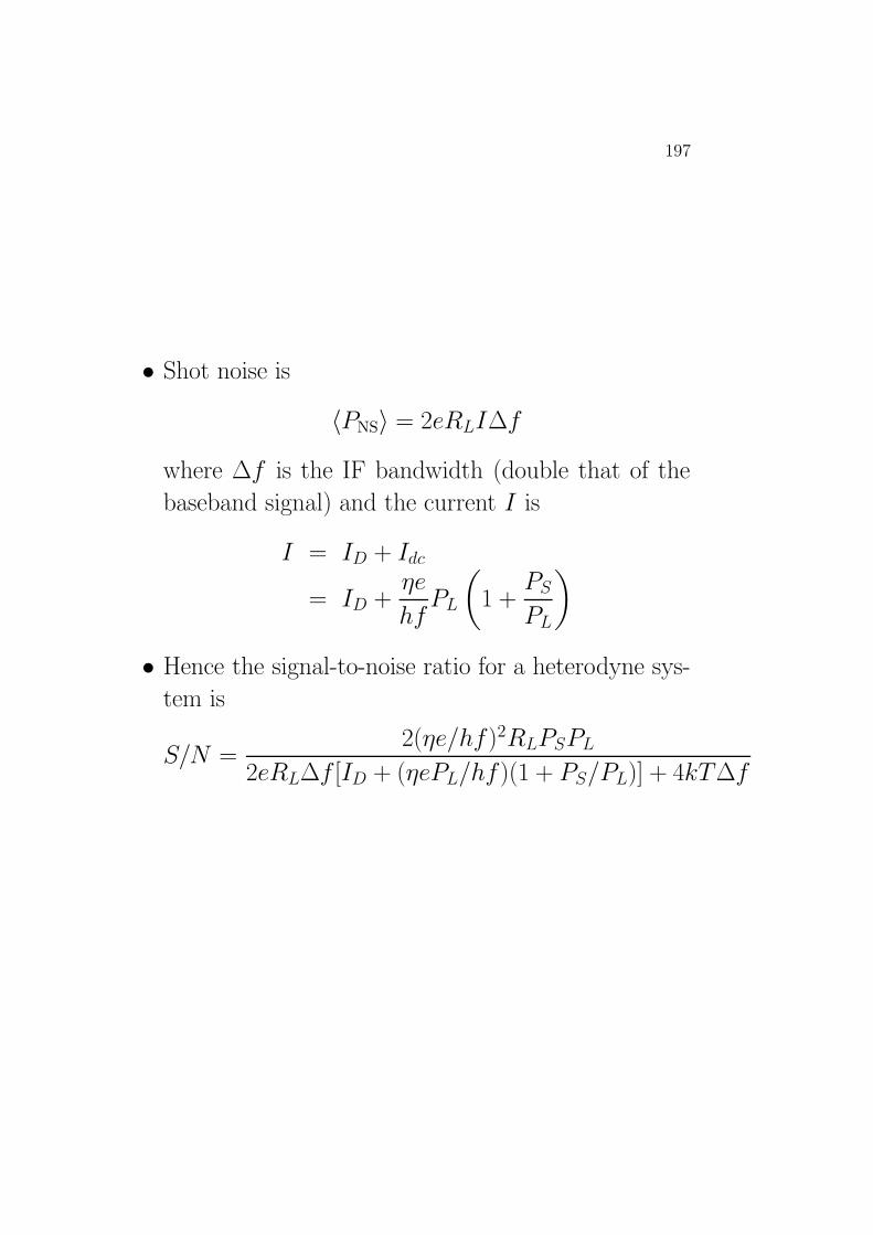
197
• Shot noise is
〈PNS〉 = 2eRLI∆f
where ∆f is the IF bandwidth (double that of the
baseband signal) and the current I is
I = ID + Idc
= ID +ηe
hfPL
(1 +
PSPL
)
• Hence the signal-to-noise ratio for a heterodyne sys-
tem is
S/N =2(ηe/hf)2RLPSPL
2eRL∆f [ID + (ηePL/hf)(1 + PS/PL)] + 4kT∆f

198
Error Rates in Digital Systems
• Bit-error-rate is equivalent to the Probability of Error
Pe in determining the binary value of each bit.
• Errors are caused by noise on the received signal.
1. Thermal Noise Limited Systems
• The decision on “0” or “1” is made by comparing
the signal current amplitude with a predetermined
threshold.
• For “0”, the noise current may increase the level be-
yond the threshold. For “1”, the noise current may
add out of phase to drop the level below the thresh-
old.

199
• With the threshold set at half the peak signal cur-
rent (ie. at 0.5is), the probability of error and the
required signal-to-noise ratio are realted by
Pe =1
2− 1
2
(0.354
√S
N
)
where the error function erf(x) is given for x ≥ 3 by
erf(x) = 1− e−x2
x√π
• For a Pe, we can obtain the required S/N and hence
the required optic power for adequate receiver sensi-
tivity
P =hf
ηe
√4kT∆f
RL
√S
N
• The number of photons received per bit for a bit
interval τ is
np = (P/hf)τ

200
2. Shot Noise Limited Systems
• Also referred to as Quantum Limited, and requires
very high receiver sensitivity.
• Post detection processing counts the number of elec-
trons produced in the photodetector. A threshold on
the count is used to determine a “0” or “1”.
• The number of photonelectrons produced in a bit
interval τ when a “1” is received is
ns =ηPτ
hf=isτ
e
• The number of photoelectrons produced when a “0”
is received is due to the dark current, and is
nn =IDτ
e

201
• Optimal threshold when “1”s and “0”s are equally
likely is set at
kT = int
1 +
nsln(1 + ns/nn)
• The disadvantage is that the optic power must be
known to set the threshold.
• For small dark current (ie. nn ≈ 0), kT = 1 and
Pe = e−ns

202
Other Sources of Noise
Modal Noise
• Modal noise causes a random variation in optic power
in multimode fibres.
• Usually experimentally determined.
• Caused by the speckle pattern in the fibre croass-
section – ie. bright spots where mode interference is
additive.
• Speckle pattern changes with wavelength changes due
to temperature, modulation etc.
• Mechanical fibre movement also affects speckle pat-
tern.
• Connectors are sensitive to changes in the speckle
pattern and randomly varying transmitter power may
result.

203
Electronic Amplifier Noise
• An electronic amplifier normally follows the photode-
tector to increase receiver gain.
• Amplifier multiply the noise and also create their own
thermal noise.
• For a given amplifier noise figure F ,
(S/N)out =1
F(S/N)in
and the signal-to-noise ratio is degraded.
• For shot noise limited systems, APDs or heterodyne
detection provides noiseless amplification.

204
Optical Amplifier Noise
• Repeaters may be implemented using optical ampli-
tiers.
• Each amplifier has a gain Gk and a noise figure
Fk =(S/N)k,in(S/N)k,out
• If the transmission loss between the kth and k+ 1th
amplifier is αk, the total noise figure of a chain of N
repeaters is
F =F1
α1+
F2
α1G1α2+ · · · + FN∏N−1
i=1 (αiGi)αN

205
Laser Noise
• Laser output will fluctuate randomly even when driven
with a constant −→ may be significant in high speed
systems.
• Described by Random Intensity Noise (RIN) which
is minimised by operating well above the laser thresh-
old current.
• Mean square RIN current is
〈i2NL〉 = RIN(ρP )2∆f
or noise electrical power
〈PNL〉 =⟨i2NL⟩RL
• RIN is often specified in dB/Hz as
RINdB/Hz = 10 log
(⟨P 2NL
⟩
P 2∆f
)
where P is the average optic power.
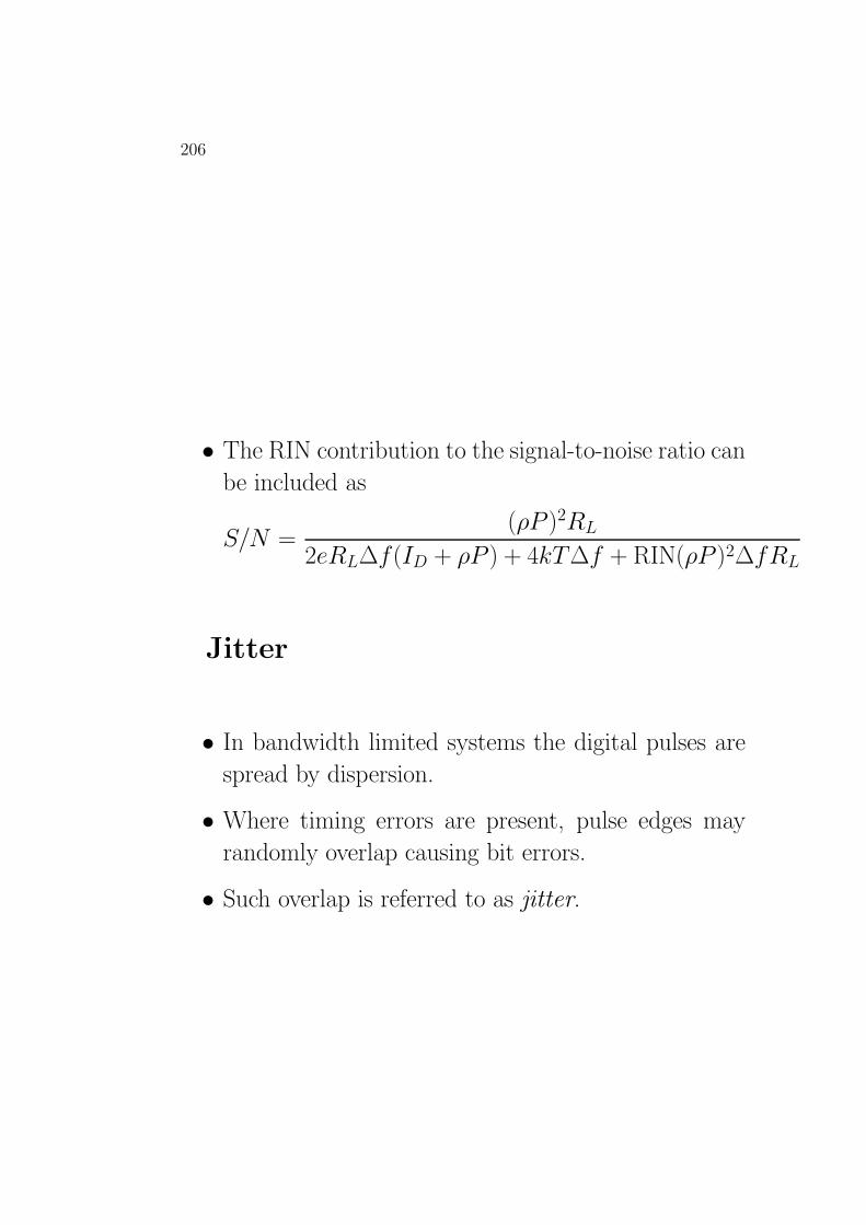
206
• The RIN contribution to the signal-to-noise ratio can
be included as
S/N =(ρP )2RL
2eRL∆f(ID + ρP ) + 4kT∆f + RIN(ρP )2∆fRL
Jitter
• In bandwidth limited systems the digital pulses are
spread by dispersion.
• Where timing errors are present, pulse edges may
randomly overlap causing bit errors.
• Such overlap is referred to as jitter.

207
Receiver Circuit Design
Front end circuitry: photodetector and first amplifier.
BJT and FET Amplifiers
• Circuits:
R
Vb
Vcc
RL
Vo
R
VbRL
Vo
Vdd

208
• Denoting RT = RL||R||Rin and C = Cd+Cin where
Rin and Cin are the input resistance and capacitance
of the BJT or FET and Cd is the photodiode junction
capacitance, the circuit limited electrical bandwidth
is
f3dB =1
2πRTCT
• The amplifiers will have a noise figure F that de-
grades the signal-to-noise ratio.
• At low modulation frequencies (below 50 MHz) FETs
have superior noise performance. Above 50 MHz
BJTs are preferred.

209
High Impedance Amplifier
• In the BJT and FET amplifiers it would be desir-
able to make RL large to improve noise performance.
However, this degrades the dynamic range and band-
width of the receiver.
• A transimpedance amplifier is used, the noise prop-
erties of which approach that of a high impedance
amplifier.
Vb V
Rfid
• The electrical bandwidth is here
f3dB =1
2πRfCf
where Cf is the feedback capacitance of the amplifier.

210
Fibre Distribution Systems
Directional Couplers
1 2
34
• Throughput Loss :
LTHP = −10 logP2
P1
• Tap Loss (coupling factor):
LTAP = −10 logP3
P1
• Directionality (isolation):
LD = −10 logP4
P1
• Excess Loss :
LE = −10 logP2 + P3
P1

211
• Directional couplers are used as power splitters, where
the splitting ratio is defined as P2/P3. For example,
a 3 dB power splitter has LTHP = LTAP = 3 dB giving
equal power from ports 2 and 3.
• An example of directional coupler construction is the
fused biconically tapered section shown below. The
length of the fused section determines LTAP.
Cladding
Cladding
Cladding
2 Core
3 Core
L

212
Duplexing Network
1 2
34
T
R
1 2
34
T
R
DC DC
Loss due to the duplexers is 6 dB.
Tree Network
Bus Bus
DC
DC
T R
1
2 3 4
NTDC T T T DC
Network loss is
L = (N − 1)LTHP + LTAP + 2NLC
where LC is the connector loss.

213
Star Network
Ring Coupler
1 2 N
1’ 2’ N’
Network Loss is
L = −10 log
(1
N
)+ LE + 2LC
Ring Network
1
2 3
4
56
• No sharing of optical power −→ large networks can
be constructed.
• Reconfigurable when nodes fail.
• Fibre Distributed Data Interface (FDDI) LAN archi-
tecture.

214
Optical Isolators
• Used to prevent optical power being reflected back
or passed to a source.
• A Faraday rotation isolator can be used.
• Non-reciprocal materials such as Yttrium Iron Gar-
net (YIG) are used to rotate the direction of polariza-
tion in a manner dependent on propagation direction.
InputPolarizer
OutputPolarizer
45 degreeFaraday Rotator

215
Analog Example
• Specification:
Transmit a 6 MHz bandwidth signal from a surveil-
lance system over a distance up to 500 m achieving
a SNR at the receiver of 50 dB.
• Proposal:
Use baseband analogue modulation, multimode fibre,
LED source, silicon PIN photodetector short wave-
length (800-900 nm) window.
Options to improve performance if needed:
– Use single mode fibre
– Use an APD
– Use s LD
– Use longer wavelength

216
Design
1. Receiver:
• Use a BJT/load resistor circuit.
• Assume 100% modulation
• Typical PIN diode characteristies at 850 nm:
Cd = 5 pF
ρ = 0.5 A/W
ID = 1 nA
=⇒ for a 6 MHz bandwidth
RL ≤ (2πCdf3dB)−1
≤ 5.3 kΩ
∴ Choose RL = 5 kΩ. Hence ∆f = 6.4 MHz. Some
lattitude for other component limitations.
• Assume the amplifier has a 3 dB noise figure at 300 K.
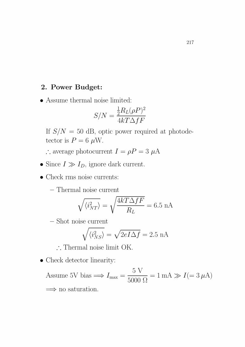
217
2. Power Budget:
• Assume thermal noise limited:
S/N =12RL(ρP )2
4kT∆fF
If S/N = 50 dB, optic power required at photode-
tector is P = 6 µW.
∴ average photocurrent I = ρP = 3 µA
• Since I ID, ignore dark current.
• Check rms noise currents:
– Thermal noise current√〈i2NT 〉 =
√4kT∆fF
RL= 6.5 nA
– Shot noise current√〈i2NS〉 =
√2eI∆f = 2.5 nA
∴ Thermal noise limit OK.
• Check detector linearity:
Assume 5V bias =⇒ Imax =5 V
5000 Ω= 1 mA I(= 3 µA)
=⇒ no saturation.

218
Choose components:
• LED
Pavg = 1 mW @ 850 nm
tr = 12 ns
∆λ = 35 nm
emitting surface diameter 50 µm.
• Multimode SI Fibre
NA = 0.24
optic f3dB × L = 33 MHz× km
Loss = 5 dB/km
Core diameter 50 µm.
• Multimode GRIN Fibre
axia NA = 0.24
optic f3dB × L = 500 MHz× km (with LD)
Loss = 5 dB/km
Core diameter 50 µm.

219
Hence:
Source power 0 dBm
Receiver power > -22.2 dBm (6 µW)
SI fibre −→ LED coupling loss η = (NA)2
• SI coupling loss: 12.4 dB
GRIN fibre −→ LED coupling loss 3 dB worse
• GRIN coupling loss: 15.4 dB
Loss due to reflectance at glass/air interface
• Reflectance loss: 0.4 dB (total)
Connector loss – assume 2 connectors
• Connector loss: 2 dB (total)
∴ SI fibre can have loss 22.2−12.4−0.4−2 = 7.4 dB.
=⇒ Max. SI fibre length 7.45 = 1.48 km
GRIN fibre can have loss 4.4 dB
=⇒ Max. GRIN fibre length 4.45 = 880 m

220
3. Bandwidth Budget.
Work in rise times:
System tslight source tLS
fibre tFphotodetector tPD
t2s = t2LS + t2F + t2PD
Assume for the system that
ts =0.35
f3dB
= 58 ns
Photodiode tPD = 2.19 RLCd = 55 ns.
[Note tPD transmit time of ≈ 1 ns
=⇒ detector is circuit limited.]
LED tLS = 12 ns.
=⇒ Allowable fibre rise time tF ≤ 14 ns.

221
Recall:
f3dB(elec.) = 0.71 f3dB(opt.)
and tF ≈ ∆τ
• For SI fibre f3dB(elec.)× L = 23.4 MHz×km
=⇒ tF/L =0.35
23.4× 106= 15 ns/km
=⇒ max. fibre length is14
15= 930 m
∗ SI fibre system is bandwidth limited.
• For GRIN fibre f3dB(elec.)× L = 355 MHz×km
∴ tmod
L= 1 ns/km with LD
But need to include material dispersion due to LED
linewidth. ( M= 90 ps/nm/km)
∴ tdis
L= M∆λ = 3.2 ns/km
tF/L =
√(tmod
K
)2
+tdis
L= 3.2 ns/km
=⇒ max. fibre length is14
3.4= 4.1 km
∗ GRIN fibre system is power limited.
∴ Either system works for 500 m path!

222
Digital Example
• Specification:
Transmit a 400 Mbps NRZ data over 100 km with a
BER of 10−9 or better.
• Proposal:
Need a fibre with very high rate-length product and
very low attenuation
=⇒ Single mode fibre at 1550 nm
+ Very fast source =⇒ Laser diode
+ Very fast detector with gain
=⇒ InGaAs APD
Try a conventional BJT receiver circuit.
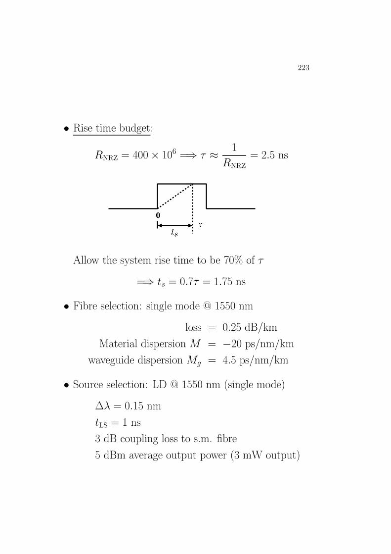
223
• Rise time budget:
RNRZ = 400× 106 =⇒ τ ≈ 1
RNRZ
= 2.5 ns
0 ÊË Ì
Allow the system rise time to be 70% of τ
=⇒ ts = 0.7τ = 1.75 ns
• Fibre selection: single mode @ 1550 nm
loss = 0.25 dB/km
Material dispersion M = −20 ps/nm/km
waveguide dispersion Mg = 4.5 ps/nm/km
• Source selection: LD @ 1550 nm (single mode)
∆λ = 0.15 nm
tLS = 1 ns
3 dB coupling loss to s.m. fibre
5 dBm average output power (3 mW output)
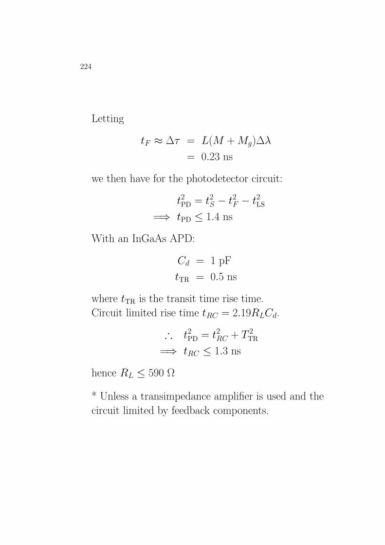
224
Letting
tF ≈ ∆τ = L(M + Mg)∆λ
= 0.23 ns
we then have for the photodetector circuit:
t2PD = t2S − t2F − t2LS
=⇒ tPD ≤ 1.4 ns
With an InGaAs APD:
Cd = 1 pF
tTR = 0.5 ns
where tTR is the transit time rise time.
Circuit limited rise time tRC = 2.19RLCd.
∴ t2PD = t2RC + T 2TR
=⇒ tRC ≤ 1.3 ns
hence RL ≤ 590 Ω
* Unless a transimpedance amplifier is used and the
circuit limited by feedback components.


225
Optical Storage
Data Channel
• To be useful, data is either
– Transmitted and used elsewhere, or
– Stored and retrieved later
Channel Errors
• Data will always be corrupted by errors in the chan-
nel
– CD-ROM scratches
– Radio interference
– Random noise on a phone line
• Is it possible to detect and correct errors?
– YES!
– Well, almost always.

226
OSI Communication Reference Model

227
Simple Error Detection
• Suppose our channel has a uniform bit error proba-
bility of 10−3
• Triple repetition
– 000 or 111
• Probability of a single or double bit error
≈ 3× 10⁻³ (Detected errors)
• Probability of a triple bit error
– 10−9 (Undetected error)
• Using triple repetition, use majority rule
– Correction rate 3× 10⁻³
– Residual error rate 3× 10⁻⁶ + 10−9
• This simple example is very inefficient
– Each channel bit represents 1/3 of a bit of useful
information
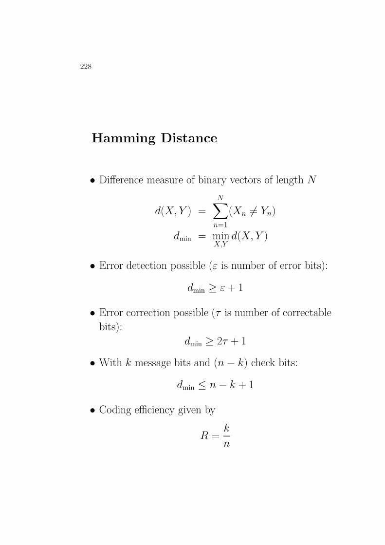
228
Hamming Distance
• Difference measure of binary vectors of length N
d(X, Y ) =
N∑
n=1
(Xn 6= Yn)
dmin = minX,Y
d(X, Y )
• Error detection possible (ε is number of error bits):
dmin ≥ ε + 1
• Error correction possible (τ is number of correctable
bits):
dmin ≥ 2τ + 1
• With k message bits and (n− k) check bits:
dmin ≤ n− k + 1
• Coding efficiency given by
R =k
n

229
Eight-to-Fourteen Modulation
• The first-line of error detection/corection codes on
CD or CD-ROM
– 8 bit codeword represented by 14 channel bits
– Choose 256 codewords with at least 4 bits differ-
ent from all other valid codewords
∗ 00011010001100
∗ 11001010101100, etc
∗ dmin = 4
∗ 512 valid codewords available
– Can detect up to 3 bit errors
– can correct 1 bit error

230
Error Correction Example
• 16 data bits with 8 parity bits
• Even parity forced in x and y
– 0,2 or 4 bits set to 1
• Any single message-bit error correctable
m1 m2 m3 m4 c1
m5 m6 m7 m8 c2
m9 m10 m11 m12 c3
m13 m14 m15 m16 c4
c5 c6 c7 c8
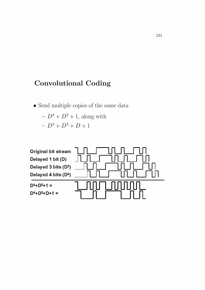
231
Convolutional Coding
• Send multiple copies of the same data
– D4 + D3 + 1, along with
– D4 + D3 + D + 1

232
Interleaving
• Error usually occur in a burst
MY**** HAS NO NOSE
• Since convolution relies on consecutive bits, we use
interleaving to break up bursty errors

233
Communication without Resend
• Broadcast data
– Digital TV
• Stored data
– CDROM or DVD
• Resend is not possible
– Require very low probability of uncorrectable er-
ror
– Requires very powerful error correction codes
Graceful Degradation
• Some data requires perfect transmission
– Text
– Binary executable programs
• In the case of multimedia, can “guess” missing con-
tent
– Repeat previous video frame section
– Repeat or silence audio
– Approximate image etc

234
CD-ROM
• Capacity 654.74 MBytes
• One spiral track of reflective pits and land
– Read by reflection of focussed laser
• Constant Linear Velocity
– Spins quickly for inner tracks, slowly for outer
tracks
• Mass produced or writable
• Data format standards, including audio
• Very high levels of error correction

235
Low Level Data Encoding Requirement
• 1. High information density
– Efficient use of medium
• Minimum intersymbol interference
– Maximise run length
• Self-clocking
– Minimise run length
• Low digital sum
– Uniform distribution of ones and zeros
Low-level Coding
• NRZ coding
– 1 is a transition between land and pit
– 0 remains as a constant land or pit
• Eight-to-Fourteen modulation
– 8 bits encoded as 14 bit word
• Three merging bits (no information)
– Limit run length and distribute 1s and 0s
• Total of 17 channel bits per octet
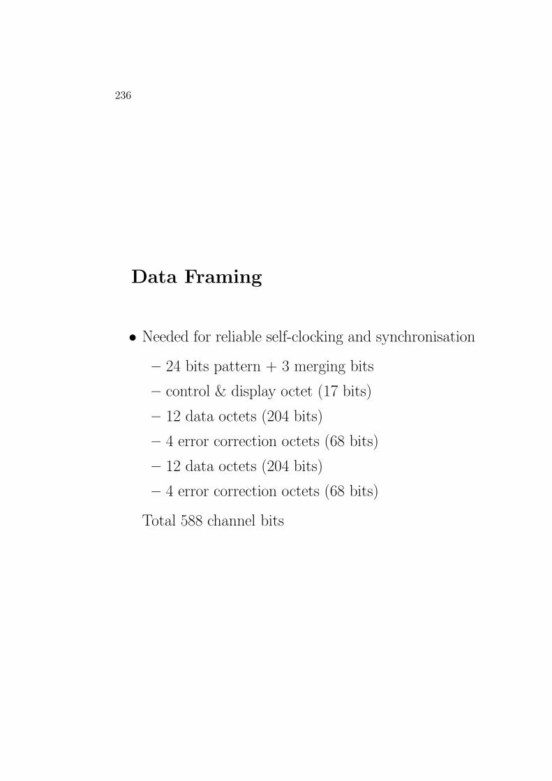
236
Data Framing
• Needed for reliable self-clocking and synchronisation
– 24 bits pattern + 3 merging bits
– control & display octet (17 bits)
– 12 data octets (204 bits)
– 4 error correction octets (68 bits)
– 12 data octets (204 bits)
– 4 error correction octets (68 bits)
Total 588 channel bits

237
First Level Error Correction
• 14 to 8 demodulation
• Reed-Solomon decoder
• Interleave
• Second Reed-Solomon decoder
• Result is a high probability of correct data
– Up to 220 octets/second raw errors (0.12% per-
fectly corrected (almost always)
CD-ROM Error Correction
• Each 2048 octet block of data is protected by
– 32 bit parity code for error detection
– 2208 bit Reed-Solomon error correction code
• Result is a much lower probability of error
– 10−9 is achievable for a CD in good condition
• Mechanical requirements
– Manufacture
– Accuracy of recording and reading mechanism
– Physical condition and wear

238
DVD-Digital Versatile Disc
• Primary application is video
– 2 hours of broadcast quality video per layer
– Up to 9 hours of VHS quality video per layer
• Other applications
– Better-than-CD audio
– Data storage
∗ 4.38 Gigabytes (Single Sided, Single Layer) to
∗ 15.90 Gigabytes (Double Sided, Double Layer)
• Data rate of 11.1 Mbit/s
– Around 5 Mbit/s for broadcast quality video
Features of DVD-Video
• Broadcast quality 2 hours pwe layer per side
– 8 hours per DS/DL disc
– 30 hours of VHS quality on DS/DL
• Uses MPEG-2 video coding
– Widescreen or standard TV
• Up to 8 audio tracks
• Seamless branching of video
• Random access

239
DVD versus CD
• Increase in capacity due to
– Smaller pit length ×2.08
∗ 0.40 to 1.87 versus 0.83 to 3.05 micron
– Tighter trach pitch ×2.16
∗ 0.74 versus 1.6 micron
– Larger data area ×1.02
– Better channel modulation ×1.06
– Better error correction ×1.32
– Less sector overhead ×1.06
• Total increase ×7

240
Example of data asymmetry
• H.261/263
– Real-time video-conferencing
– Asymmetric processing, symmetric channel
– Very powerful data processing at encoder
– These days, can be handled in real time by a
modern PC
• MPEG-1
– CD-ROM based video storage & retrieval
– Asymmetric processing and channel
– 10 minutes of video may require hours of process-
ing on a PC
Conclusions
• Error detection and correction is needed beacuse stor-
age and transmission is not perfect
• CD, CD-ROM and DVD have different error correc-
tion requirements but operate on the same principles