Operation and application of the Sentron CSA-1V-SO … · Current Sensing with the CSA-1V Hall IC...
14
Current Sensing with the CSA-1V Hall IC AN_102 Aug 17, 2004 1 Operation and application of the Sentron CSA-1V-SO surface mount Current Sensor Contents Topic Page Introduction 2 Basic Operation 2 Basic Electrical Connections 2 Current-Voltage transfer functions 3 Accuracy considerations 5 Saturation Limits 5 Accommodating various current limits 5 High output, improved accuracy midrange current measurements 7 Stray magnetic field interference 8 Shielding 9 Multiple current circuits 9 Response time 11 Interface circuits 11 Test PCB’s 12 Conversion Table for common magnetic terms 14 SENTRON AG, Baarerstrasse 73, CH-6300, Zug, SWITZERLAND Tel: +41 41 7112170 Fax: +41 41 7112188. Email: [email protected] GMW P.O. Box 2578, Redwood City, CA 94064, USA. Tel+1 (650) 802-8292. Fax: +1 (650) 802-8298. Email: [email protected]
Transcript of Operation and application of the Sentron CSA-1V-SO … · Current Sensing with the CSA-1V Hall IC...

Current Sensing with the CSA-1V Hall IC AN_102 Aug 17, 2004
1
Operation and application of the
Sentron CSA-1V-SO surface mount Current Sensor
Contents Topic Page Introduction 2 Basic Operation 2 Basic Electrical Connections 2 Current-Voltage transfer functions 3 Accuracy considerations 5 Saturation Limits 5 Accommodating various current limits 5 High output, improved accuracy midrange current measurements 7 Stray magnetic field interference 8 Shielding 9 Multiple current circuits 9 Response time 11 Interface circuits 11 Test PCB’s 12 Conversion Table for common magnetic terms 14
SENTRON AG, Baarerstrasse 73, CH-6300, Zug, SWITZERLAND Tel: +41 41 7112170 Fax: +41 41 7112188. Email: [email protected] GMW P.O. Box 2578, Redwood City, CA 94064, USA. Tel+1 (650) 802-8292. Fax: +1 (650) 802-8298. Email: [email protected]

Current Sensing with the CSA-1V Hall IC AN_102 Aug 17, 2004
2
Introduction The CSA-1V is an integrated circuit combining Hall devices and Sentron’s patented IMC* Hall technology. The Hall-sensor is fabricated using a conventional CMOS technology with an additional ferromagnetic layer. The ferromagnetic layer is used as a magnetic flux concentrator providing a magnetic gain of about 10, to increase the output signal without increasing the inherent sensor electrical noise. The CSA-1V is a SOIC-8 packaged device suitable for surface mount PCB construction and miniaturization. The CSA-1V is a very simple device to use and provides an analog output voltage proportional to the magnetic field generated by the current flowing through a conductor near the IC. The IC can sense DC currents as well as AC currents up to 100 kHz. It is particularly appropriate for on-board DC current measurement with ohmic isolation, fast response, small package size and low assembly cost. Basic operation. The CSA-1V senses current by converting the magnetic field generated by current flowing through a conductor to a voltage which is proportional to that field. The magnetic field at distance r from an ideally thin, straight and infinitely long current conductor carrying a current I is given by
r2IrHπ
=)(
In a vacuum (or air) the magnetic induction (or flux density) B can be calculated from H by multiplication with the permeability
with
See section on Current to Voltage transfer functions for direct relationship between current and the CSA-1V * IMC = Integrated Magnetic Concentrator Example: Flux density at a distance r = 2 mm from a current conductor carrying 20 Amperes:
mTm
AAmVsB 0.2
002.0220104 7 =⋅
⋅⋅= −
ππ
The CSA-1V can be used to measure current in an adjacent wire as shown in Figure 1 or in PCB trace conductors mounted below the IC as shown in Figure 2. The output vs. direction of current will be reversed for these two illustrations because the direction of the magnetic field is dependant on whether the IC is above the wire or below it, see figure 5.
Figure 1- Sensing current in a conductor
Figure 2 – Sensing current in a PCB trace Basic electrical connections The connection diagram is shown in figure 3. The CSA-1V has two output configurations; Single ended output (Vout) which provides a 0 to 5V analog output with respect to ground and a differential output (Vout
diff) which provides a 0 +/- 2.5 volts with respect to an internal reference voltage (CO_OUT).
AmVs104 7
0−⋅= π
µHB 0µ=
SENTRON AG, Baarerstrasse 73, CH-6300, Zug, SWITZERLAND Tel: +41 41 7112170 Fax: +41 41 7112188. Email: [email protected] GMW P.O. Box 2578, Redwood City, CA 94064, USA. Tel+1 (650) 802-8292. Fax: +1 (650) 802-8298. Email: [email protected]
Current Sensing with the CSA-1V Hall IC AN_102 Aug 17, 2004
3
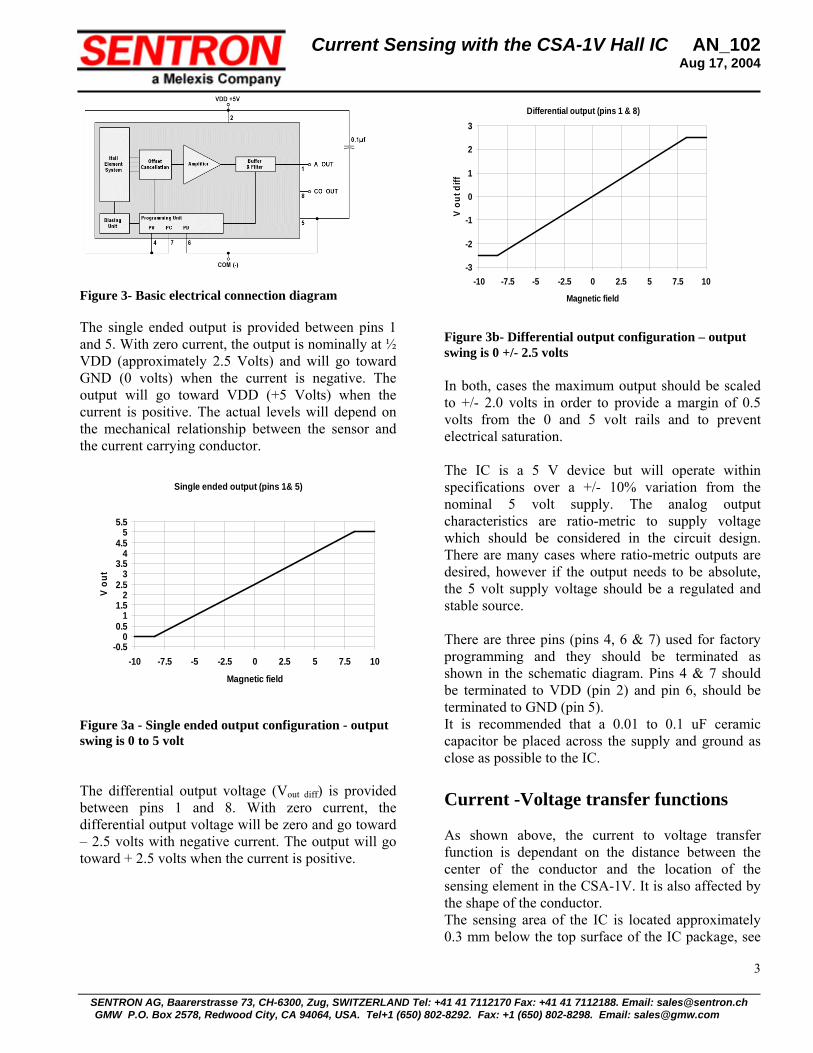
Figure 3- Basic electrical connection diagram The single ended output is provided between pins 1 and 5. With zero current, the output is nominally at ½ VDD (approximately 2.5 Volts) and will go toward GND (0 volts) when the current is negative. The output will go toward VDD (+5 Volts) when the current is positive. The actual levels will depend on the mechanical relationship between the sensor and the current carrying conductor.
Single ended output (pins 1& 5)
-0.50
0.51
1.52
2.53
3.54
4.55
5.5
-10 -7.5 -5 -2.5 0 2.5 5 7.5 10
Magnetic field
V ou
t
Figure 3a - Single ended output configuration - output swing is 0 to 5 volt The differential output voltage (Vout diff) is provided between pins 1 and 8. With zero current, the differential output voltage will be zero and go toward – 2.5 volts with negative current. The output will go toward + 2.5 volts when the current is positive.
Differential output (pins 1 & 8)
-3
-2
-1
0
1
2
3
-10 -7.5 -5 -2.5 0 2.5 5 7.5 10
Magnetic field
V ou
t diff
Figure 3b- Differential output configuration – output swing is 0 +/- 2.5 volts In both, cases the maximum output should be scaled to +/- 2.0 volts in order to provide a margin of 0.5 volts from the 0 and 5 volt rails and to prevent electrical saturation. The IC is a 5 V device but will operate within specifications over a +/- 10% variation from the nominal 5 volt supply. The analog output characteristics are ratio-metric to supply voltage which should be considered in the circuit design. There are many cases where ratio-metric outputs are desired, however if the output needs to be absolute, the 5 volt supply voltage should be a regulated and stable source. There are three pins (pins 4, 6 & 7) used for factory programming and they should be terminated as shown in the schematic diagram. Pins 4 & 7 should be terminated to VDD (pin 2) and pin 6, should be terminated to GND (pin 5). It is recommended that a 0.01 to 0.1 uF ceramic capacitor be placed across the supply and ground as close as possible to the IC. Current -Voltage transfer functions As shown above, the current to voltage transfer function is dependant on the distance between the center of the conductor and the location of the sensing element in the CSA-1V. It is also affected by the shape of the conductor. The sensing area of the IC is located approximately 0.3 mm below the top surface of the IC package, see
SENTRON AG, Baarerstrasse 73, CH-6300, Zug, SWITZERLAND Tel: +41 41 7112170 Fax: +41 41 7112188. Email: [email protected] GMW P.O. Box 2578, Redwood City, CA 94064, USA. Tel+1 (650) 802-8292. Fax: +1 (650) 802-8298. Email: [email protected]

Current Sensing with the CSA-1V Hall IC AN_102 Aug 17, 2004
4
figure 4. The output will produce a positive output when the magnetic field vector, B, is in the direction shown.
0.065[1.66]
1 32
8 67
B
0.012[0.30]
4
5
Figure 4- Direction of sensitivity and location of sensing element Figure 5 illustrates the magnetic flux lines from two different examples of conductor shapes. The upper conductor is a circular wire and the lower is a wide trace on a PCB. Notice that the direction of the magnetic flux is reversed for the two conductors assuming the current is flowing out of the page.
PCB conductor
B d
Figure 5 – Shape and direction of magnetic field from two different conductor shapes. Circular conductor on top of IC. The CSA-1V differential output voltage for a circular conductor (wire) located on top of the IC can be approximated with the following equation:
)3.0(*060.0mmd
IV diffout +≈
d = distance (mm) from chip surface to center of
wire as shown in figure 5 in mm I = Current in conductor
Example for a wire on top of IC: If the current in the conductor is 25 amps and the distance of the wire from the
surface of the IC is 1.0 mm, then the differential output voltage will be:
voltsV diffout 15.1)3.01(
25*060.0≅
+≈
Sensitivity 300V/T
0
500
1000
1500
2000
2500
0.1 1 10
distance chip surface to conductor center [mm]
Sens
or o
utpu
t vol
tage
[mV] 1A
2A
5A
10A
25A
50A
100A
Fig. 6- CSA-1V sensor output voltage is dependent on the applied current in the current conductor (wire on the top of the sensor) and the distance between chip surface and center of the current conductor. Flat Conductor on PCB under the IC. The CSA-1V output for the flat conductor directly below the IC can be approximated with the following equation:
IampmVV diffout *40≈
I = Current in conductor
Example for flat conductor located directly under the CSA-1V:
If the current, I, is +15 amps (positive current in this illustration will be current flowing out of the page), the output will be:
voltsampsampmVV diffout 60.0)15(*40 ≅+≈
If the current, I, is -15 amps the differential output voltage will be:
SENTRON AG, Baarerstrasse 73, CH-6300, Zug, SWITZERLAND Tel: +41 41 7112170 Fax: +41 41 7112188. Email: [email protected] GMW P.O. Box 2578, Redwood City, CA 94064, USA. Tel+1 (650) 802-8292. Fax: +1 (650) 802-8298. Email: [email protected]
Current Sensing with the CSA-1V Hall IC AN_102 Aug 17, 2004
5
voltsampsampmVV diffout 60.0)15(*40 −≅−≈
The sensitivity to a flat conductor is greater when located under the IC than when it’s located on the top of the IC. This is due to the internal construction of the IC and the location of the Hall elements with respect to the integrated magnetic concentrator. Accuracy considerations The absolute accuracy of the current measurement is dependant on several factors. One factor is the variation in magnetic sensitivity of the CSA-1V which is +/- 3%. Another factor is the offset voltage which is specified to 10mV max. Generally speaking, the higher the current and closeness of the conductor to the IC, the more accurate the reading will be. However the limits of electrical and magnetic saturation need to be respected. At small currents where the output voltage is low, the 10 mV offset could contribute to significant error in the measurement. For example: if the maximum output voltage is 200 mV, the 10 mV offset could introduce a 5% error in the measurement. With 3% sensitivity variation and 5% offset error, the maximum error for a low current measurement could be as high as 8%. If the circuit is configured to provide an output of 2.0 volts full scale, then the maximum error would be +/- 3.5%. The position of the wire or conductor over the sensor will have an impact on the accuracy. Any change in distance from the IC face will change the output and any side to side movement will also change the output, thereby contributing to the potential error. A single wire will be more sensitive to side to side movement than the flat bus wire. The installation should assure there is no movement in the physical location of the conductor and that the conductor position is the same for each part in a production run. Increased accuracy can be acquired by using two ICs as shown in figures 7, 10 & 11 to cancel out the potential affect of stray fields and then adjusting out the net DC offset from the two CSA-1Vs. The total error from this configuration is equal to the error of the CSA-1V’s sensitivities which is 2%, even at low current levels.
Saturation Limits The CSA-1V has excellent linearity from zero to magnetic fields of 5 mT (50 Gauss) and will reach electrical saturation at 8.3 mT (83 Gauss). The device will not be damaged or upset by magnetic fields up to 1T (10,000 Gauss). Therefore high current surges will not upset or damage the device and recovery from these conditions occurs in microseconds. Accommodating various current ranges. Low current – 1-2 Amps To increase the signal level for low current sensing circuits, a coil like circuit land pattern can be laid out on the PCB to produce a number of loops as shown in figure 7. With 4 loops, the magnetic field is increased by a factor of 4. If two devices are used as shown below, the outputs can be added together with a summing circuit illustrated in Fig 7a, thereby doubling the signal level for a given current. See figure 7a. The offset voltage and stray field effect can have a major impact on the linearity and or linearity for low current measurements. Therefore it is important to eliminate or minimize both the DC offset voltage and any stray field effect that may be present. The advantage of the two device configuration is common mode stray fields will be cancelled out and any DC offset can be adjusted out with the post circuit shown in figure 7a.
Figure 7 – Increasing signal level with multiple loops
SENTRON AG, Baarerstrasse 73, CH-6300, Zug, SWITZERLAND Tel: +41 41 7112170 Fax: +41 41 7112188. Email: [email protected] GMW P.O. Box 2578, Redwood City, CA 94064, USA. Tel+1 (650) 802-8292. Fax: +1 (650) 802-8298. Email: [email protected]

Current Sensing with the CSA-1V Hall IC AN_102 Aug 17, 2004
6
(CSA-1)
6
(CSA-1)
6
Bottom Layer
5
2 4
C1
GND 50.1uF
+5V (VDD)2 4
Top Layer
- Vout
Output = -[ (A-OUT1) + (A-OUT2)]
U2
8
17
(A-OUT2)
Current trace
+
100 K100 K
100 K
U1
8
17 (A-OUT1)
+Supply
+Supply
100 K 100 K
Offset null adjustment
2 K
I
Figure 7a- Summing circuit for dual CSA-1V’s in an output voltage doubling and noise cancellation configuration The differential output voltage for a single channel configuration can be approximated with the following equation:
ampsInampsmVV loopsdiffout **40≈
Where: n = number of loops I = current in conductors
Example:
If n = 4 and I = +/- 2 amps
voltsampsampsmVV diffout 32.0/2/*4*40 −+≅−+≈
Medium Current – 10 to 20 amps
With a single conductor located on the PCB, currents in the range of 10 to 20 amps can be measured. The sizing of the PCB trace needs to take in account the current handling capability and the total power dissipated. The PCB trace needs to be thick enough and wide enough to handle 20 amps.
Figure 8 – Medium range current sensing on PCB
The differential output voltage for this configuration can be approximated by the following equation:
ampsIampsmVV diffout *40≈
Increased output level for medium current The sensitivity (mV/Amp) can be increased by a factor of approximately 3 by configuring the PCB layout per figure 8a. This configuration increases the magnetic field for a given current by placing the IC within a loop. This loop is created by using traces on both sides of a PCB and a jumper wire mounted over the IC.
Figure 8a – PCB layout with jumper to increase sensitivity. The current flow through the circuit is shown in figure 8b. The current flows from left wire through a trace on the bottom side of the PCB and directly under the CSA-1V and then up and over the IC through the jumper wire and back under the CSA-1V through the top layer trace and out through the right wire.
SENTRON AG, Baarerstrasse 73, CH-6300, Zug, SWITZERLAND Tel: +41 41 7112170 Fax: +41 41 7112188. Email: [email protected] GMW P.O. Box 2578, Redwood City, CA 94064, USA. Tel+1 (650) 802-8292. Fax: +1 (650) 802-8298. Email: [email protected]

Current Sensing with the CSA-1V Hall IC AN_102 Aug 17, 2004
7
Figure 8b – Current flow under and around the CSA-1V increases magnetic flux density in the chip. Each conductor creates a magnetic flux that is sensed by the IC as shown in figure 8c. The three add together and increase the output signal by a factor of approximately three. The actual gain depends on the thickness of the PCB. A 0.03125 thick PCB will create a 120 mV/ Amp sensitivity level. A 0.0625 thick PCB will have a slightly lower level because the bottom conductor will be further away and it’s contribution to the total flux density at the chip will be less.
Figure 8c- Magnetic flux generated by the jumper, upper trace and lower trace add together at the sensitive area of the chip.
ampsIampsmVV diffout *120≈
High output, improved accuracy mid-range current measurement. A technique to increase the output and minimize the stray field effect is shown in figure 9. This technique incorporates two CSA-1Vs using the scheme shown in figure 8a. By placing two of these layouts parallel to each other, but opposite orientation will create
equal but opposite outputs for stray fields that can be cancelled out in a post summing circuit. The outputs from the two CSA-1V’s can be added together to produce an output sensitivity level of approximately 0.24 V/Amp. A +/- 10 amp current will produce a 2.5 V +/- 2.4 V output. Using the circuit shown in figure 7a , a very accurate high level current measurement can be made with this configuration.
Current Flow
Jumper
Figure 9 - Dual CSA-1V’s with the loop technique to improve the output level and minimize stray field effect. High Current – 20 to 100 amps
High currents can be measured by placing a formed copper bus bar over the IC as shown in Figure 10. The distance and size will depend on the full scale output desired. An approximation of differential output voltage can be obtained with the following equation:
( )3.0
*40
+≈
d
ampsIAmmmV
V diffout
Where d =distance (mm) between conductor center and CSA-1V surface and I = current in conductor
d
SENTRON AG, Baarerstrasse 73, CH-6300, Zug, SWITZERLAND Tel: +41 41 7112170 Fax: +41 41 7112188. Email: [email protected] GMW P.O. Box 2578, Redwood City, CA 94064, USA. Tel+1 (650) 802-8292. Fax: +1 (650) 802-8298. Email: [email protected]

Current Sensing with the CSA-1V Hall IC AN_102 Aug 17, 2004
8
Figure 10- High current application using a formed buss bar over IC. Example:
If I = +/- 80 amps and d = 1 mm then
( ) voltsV diffout 46.23.1
80*40±≈
±≈
Another method of measuring high currents on PCB’s is to use a large thick gauge copper trace capable of carrying the current on the opposite side of the PCB. The CSA-1V should be located near the center of the trace, however because the trace is wide, the output is less sensitive to location on the PCB.
Figure 10a- High current application using a wide heavy conductor on the opposite of PCB. Stray magnetic field interference. The CSA-1V is an open loop magnetic sensor and will respond to any magnetic field that is in the direction of sensitivity (across the chip). Stray fields from other sources, such as transformers, adjacent current carrying conductors and magnetic circuitry can cause noise problems if they are too close to the sensor. There are several things that can be done to
minimize the interference. By using two devices as shown in figure 7, 9, 11 & 12, common mode magnetic fields are cancelled out with the added advantage of a two fold increase in signal. Placing adjacent wires or PCB traces at right angles to the IC’s direction of sensitivity can also minimize the interference, see figure 16. Because the magnetic field drops off dramatically as a function of distance, locating the sensor as far away from the source is also a way of reducing the interference noise.
Figure 11- Stray fields generate equal and opposite voltages in the two CSA-1V’s and are cancelled out by summing the differential outputs from the two devices.
Figure 12 - This configuration provides excellent stray field cancellation and significant improvement in the signal level by making 4 loops per layer for a total of 16 loops. Implementing stray field cancellation techniques and signal amplification via multiple loops should be considered when using the CSA-1V sensor to measure low currents in the range 1-5 amps. Signal to noise ratio will be greatly improved with the incorporation of these techniques.
CSA-1V
Stray fields
Stray fields
Wide and thick copper trace
SENTRON AG, Baarerstrasse 73, CH-6300, Zug, SWITZERLAND Tel: +41 41 7112170 Fax: +41 41 7112188. Email: [email protected] GMW P.O. Box 2578, Redwood City, CA 94064, USA. Tel+1 (650) 802-8292. Fax: +1 (650) 802-8298. Email: [email protected]

Current Sensing with the CSA-1V Hall IC AN_102 Aug 17, 2004
9
Shielding Shield on top of bus bar
A level of shielding, as shown in fig. 13, can be obtained by placing a small (approximately 1cm2) ferromagnetic metal plate on the opposite side of the conductor from the CSA-1V. Mu-metal is an excellent choice because of its high permeability at low field strengths. The plate will have the affect of concentrating the flux from the field generated by the current in the trace and provide shielding by deflecting stray fields from the sensor. An additional advantage with this shielding technique is an increased level of signal by a factor of 30% to 50% for a given current.
Figure 13 – Shielding the CSA-1V from stray fields. In the configuration using a bus bar, Shielding and increased signal level can be obtained by placing the shield on top of the bus bar as shown in Fig 13a.
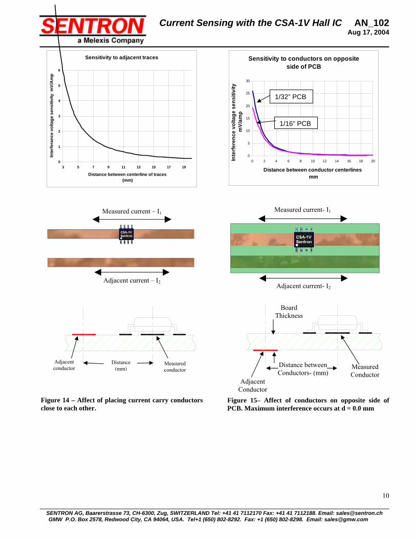
Figure 13a – Adding shielding to the top bus bar configuration increases signal level significantly and minimizes the stray field interference. CSA-1V Multiple current circuits Often it will be desirable to monitor several currents on one PCB assembly or there are other current carry traces near by. Because these devices measure the magnetic fields generated by the traces or wires located in close proximity to the sensors, they will also sense magnetic fields from adjacent conductors if the fields generated by these conductors are large enough. It is always good practice to maintain as much spacing as possible between sensors and adjacent wires. Alternatively, running traces at right angles will minimize any pickup from adjacent traces. The amount of potential interference can be estimated from the graphs in the following figures.
Field from PCBStray
Figure 14 shows the affect of other current conductors which are parallel and placed on the same side of the PCB. The affect is minimal, <5% at distance of 6 mm (≈1/4”). Figure 15 shows the affect of current conductors which are parallel but on the opposite side of the PCB. The worst condition is when the conductor is placed directly under the IC (d = 0.0).
Magnetic shield Current carrying
CSA- PCB
SENTRON AG, Baarerstrasse 73, CH-6300, Zug, SWITZERLAND Tel: +41 41 7112170 Fax: +41 41 7112188. Email: [email protected] GMW P.O. Box 2578, Redwood City, CA 94064, USA. Tel+1 (650) 802-8292. Fax: +1 (650) 802-8298. Email: [email protected]
Current Sensing with the CSA-1V Hall IC AN_102 Aug 17, 2004
10
Sensitivity to adjacent traces
0
1
2
3
4
5
6
3 5 7 9 11 13 15 17 19
Distance between centerline of traces(mm)
Inte
rfera
nce
volta
ge s
ensi
tivity
mV/
Am
p
Figure 14 – Affect of placing current carry conductors close to each other.
Sensitivity to conductors on opposite side of PCB
0
5
10
15
20
25
30
0 2 4 6 8 10 12 14 16 18 20
Distance between conductor centerlines mm
Inte
rfere
nce
volta
ge s
ensi
tivity
m
V/am
p
1/32” PCB
1/16” PCB
Measured current- I1
Figure 15– Affect of conductors on opposite side of PCB. Maximum interference occurs at d = 0.0 mm
Measured Conductor
Adjacent Conductor
Distance between Conductors- (mm)
Board Thickness
Measured current – I1
Adjacent current- I2Adjacent current – I2
Adjacent conductor
Distance (mm)
Measured conductor
SENTRON AG, Baarerstrasse 73, CH-6300, Zug, SWITZERLAND Tel: +41 41 7112170 Fax: +41 41 7112188. Email: [email protected] GMW P.O. Box 2578, Redwood City, CA 94064, USA. Tel+1 (650) 802-8292. Fax: +1 (650) 802-8298. Email: [email protected]

Current Sensing with the CSA-1V Hall IC AN_102 Aug 17, 2004
11
Figure 16 – Placing traces at right angles will significantly reduce any cross talk between sensors. Response time The CSA-1V has a wide bandwidth of 100 KHz and a response time of 6 microseconds. The response time of the sensor consists of two components. One is the Hall elements scan rate which takes up to 3 microseconds and the output driver rise time which is 3 microseconds. See figure 17.
Figure 17 – CSA-1V response to a current pulse.
Interface Circuits I1The following are some examples of interface circuits that can be used with the CSA-1V’s to provide level shifting, differential to single ended and amplification. The output voltage is ratiometric to the supply voltage and with VDD = 5.0VDC, it can swing between 0 and 5 volts (minus 50 mV). It is recommended that the output level be no more than 2.5 +/- 2.0 volts to prevent electrical saturation and non-linearity
I2
.
Fig 18 – Direct Differential Output
A-OUT
CO-COM
7 1
8
U1
42+5V (VDD)
0.1uF5GND
C1
6
(CSA-1V)
Full Scale output = 0 +/- 2.5 Volts
V out = A_OUT - CO_
GND
A-OUT7 1
8
U1
42+5V (VDD)
0.1uF5
GND
C1
6
(CSA-1V)
Fig 19 – Direct Single ended Output
Full Scale output = 2.5 +/- 2.5 Volts
Input current pulse
-
+
200K
+Supply
100K
100K
200K
(CSA-1V)U1
1742
C1
5 6 8
+5V (VDD)
GND 0.1uF
A_OUT
CO_COM Vout= -2*[ (A_OUT) - (CO_OUT)]
Fig 20 – Differential to single ended, 0-5 V swing for DC currents
peak value = 80 A
CSA-1V Output voltage
V out = A_OUT
response time 3 µs
Full Scale output = 0 +/- 5.0 Volts
rise time 3 µs
Note: DC flow should be configured to create a negative going A_OUT
SENTRON AG, Baarerstrasse 73, CH-6300, Zug, SWITZERLAND Tel: +41 41 7112170 Fax: +41 41 7112188. Email: [email protected] GMW P.O. Box 2578, Redwood City, CA 94064, USA. Tel+1 (650) 802-8292. Fax: +1 (650) 802-8298. Email: [email protected]

Current Sensing with the CSA-1V Hall IC AN_102 Aug 17, 2004
12
1
8
742
56
U1(CSA-1V)
C10.1uF
+5V (VDD)
GND (CO_OUT1)
(A_OUT1)
(A_OUT2)
(CO_OUT2)
Current trace
42 7 1
865
U2(CSA-1V)
100K 100K
1K
1K
Vout
+Supply
-
+ Vout = - [ (A-OUT1) - (A-OUT2)]
+(CO_OUT1 + C_OUT2)/2
100K
100K Note: A_OUT1 and A_OUT2 are configured to have opposite polarities for the same current
Fig 21 – Differential to single ended, 2-5 V +/- 2.5 swing
for AC currents
Note: A_OUT1 and A_OUT2 are configured to have
opposite polarities for the same current200
Offset null adjustment
100K100 K+5V
+Supply
(A-OUT1)7 1
8
U1
100K
100K 100K
+
Current trace
(A-OUT2)7 1
8
U2
Vout= -[ (A-OUT1) - (A-OUT2)]
+ 1/2 VDD +/- Adj
-
42+5V (VDD)
0.1uF5GND
C1
42
5
6(CSA-1V)
6(CSA-1V)
Fig 22 – Differential to single ended, 2-5 V +/- 2.5 swing
for AC currents with DC offset adjustment. Test PCB’s The following test PCB’s and application notes are available for evaluating the CSA-1V in various current sensing applications and configurations.
AN_103 - Single or Dual CSA-1V’s. Medium current range ( 5 - 20 Amps). Stray Field cancellation and double sensitivity with Dual configuration.
Full Scale output = 2.5 +/- 2.5 Volts
U1 CSA-1V
C1 .1uF
Top View of PCB
Botttom view of PCB
Full Scale output = 2.5 +/- 2.5 Volts U2
CSA-1
AN_106 - Single or Dual CSA-1V’s. Lower current ranges (0.5 - 5 Amps). Stray field cancellation and double sensitivity with Dual configuration.
Top View of PCB
SENTRON AG, Baarerstrasse 73, CH-6300, Zug, SWITZERLAND Tel: +41 41 7112170 Fax: +41 41 7112188. Email: [email protected] GMW P.O. Box 2578, Redwood City, CA 94064, USA. Tel+1 (650) 802-8292. Fax: +1 (650) 802-8298. Email: [email protected]

Current Sensing with the CSA-1V Hall IC AN_102 Aug 17, 2004
13
Bottom View of PCB
AN_107 – High current Sensing (Up to 50 Amps)..
Top View of PCB
Bottom View of PCB
Typical Assembly
AN_108 – Medium current range sensing with loop to increase sensitivity by a factor of three (approximately 120 mV/Amp). Typical 2 to 20 Amps
Top View of PCB
Bottom View of PCB
SENTRON AG, Baarerstrasse 73, CH-6300, Zug, SWITZERLAND Tel: +41 41 7112170 Fax: +41 41 7112188. Email: [email protected] GMW P.O. Box 2578, Redwood City, CA 94064, USA. Tel+1 (650) 802-8292. Fax: +1 (650) 802-8298. Email: [email protected]
Current Sensing with the CSA-1V Hall IC AN_102 Aug 17, 2004
14
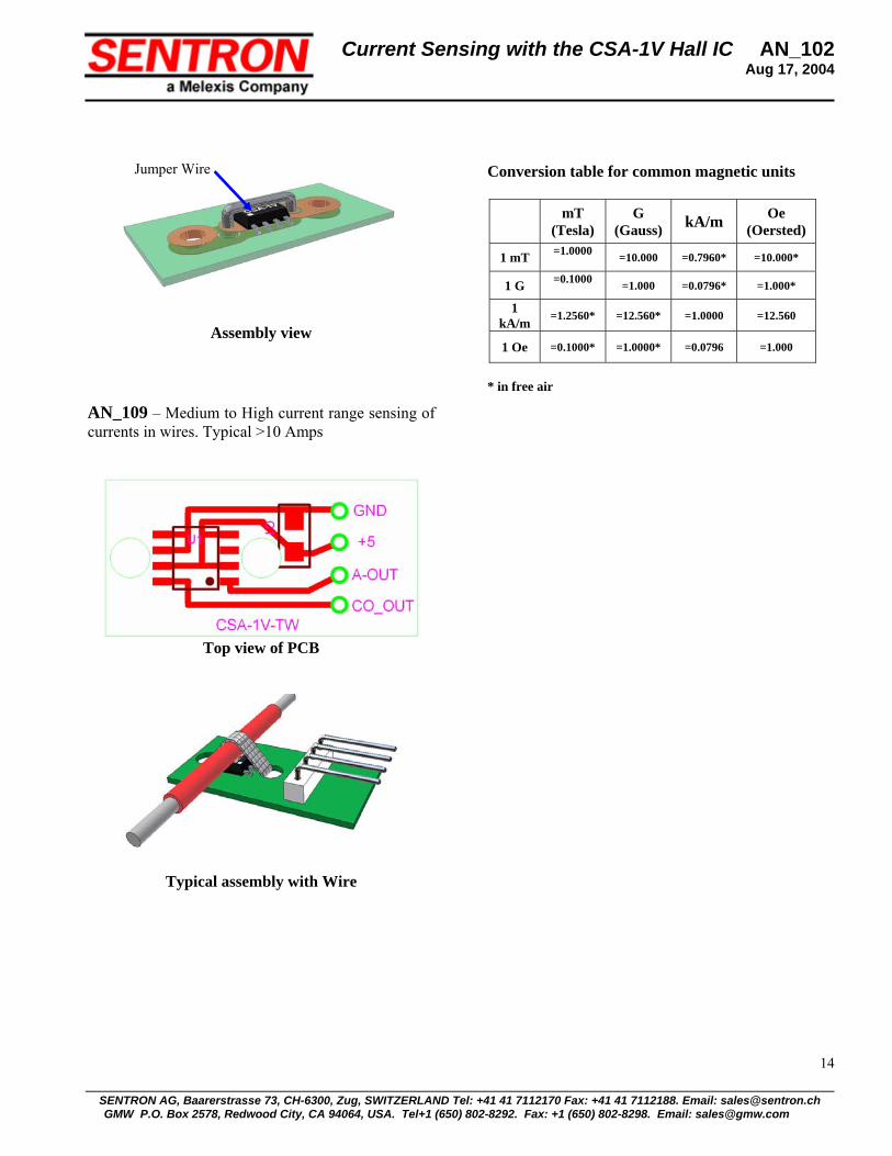
Assembly view AN_109 – Medium to High current range sensing of currents in wires. Typical >10 Amps
Top view of PCB
Typical assembly with Wire
Jumper Wire Conversion table for common magnetic units
mT (Tesla)
G (Gauss) kA/m Oe
(Oersted)
1 mT =1.0000 =10.000 =0.7960* =10.000*
1 G =0.1000 =1.000 =0.0796* =1.000*
1 kA/m =1.2560* =12.560* =1.0000 =12.560
1 Oe =0.1000* =1.0000* =0.0796 =1.000
* in free air
SENTRON AG, Baarerstrasse 73, CH-6300, Zug, SWITZERLAND Tel: +41 41 7112170 Fax: +41 41 7112188. Email: [email protected] GMW P.O. Box 2578, Redwood City, CA 94064, USA. Tel+1 (650) 802-8292. Fax: +1 (650) 802-8298. Email: [email protected]