OneTechnologyWay P.O.Box9106 Norwood,MA 02062 … · OneTechnologyWay•P.O.Box9106 ... by Brad...
18
AN-1354 APPLICATION NOTE One Technology Way • P.O. Box 9106 • Norwood, MA 02062-9106, U.S.A. • Tel: 781.329.4700 • Fax: 781.461.3113 • www.analog.com Integrated ZIF, RF to Bits, LTE, Wide Area Receiver Analysis and Test Result by Brad Brannon, Kenny Man, Nikhil Menon, and Ankit Gupta Rev. 0 | Page 1 of 18 INTRODUCTION This application note references the 3GPP TS 36 series documents and various Analog Devices, Inc., data sheets, characterization reports, and lab test results. The key focus is on the analysis and test result of an integrated, zero intermediate frequency (ZIF), RF to bits, IC (AD9371) based radio receiver for multicarrier, wide area LTE operations. Figure 1 and Figure 2 show the general assumed architecture for the discussion. Figure 2 details what is generally found in an AD9371 based radio. The key components include a duplexer, analog front end (AFE), RF surface acoustic wave (SAW) filter, and AD9371 integrated radio. Figure 3 shows the lab setup for system performance testing. AD9371 Rx AFE DUPLEXER FROM ANTENNA CONNECTOR 13042-001 Figure 1. General Architecture of Receiver ADC R IN R IN DIGITAL DECIMATION, PFIR, DC-OFFSET QEC, TUNING, RSSI, OVERLOAD ADC LO BUFFER ATTENUATION Rx1 Rx2 BALUN MATCH Tx REJECTION G LNA = +20.0dB NF = 0.5dB ANTENNA PORT SYNTH VCO PA LNA 13042-002 Figure 2. Radio Receiver Block Diagram VECTOR SIGNAL GENERATOR WANTED SIGNAL FREQUENCY = WAVEFORM = POWER = VECTOR SIGNAL GENERATOR BLOCKING SIGNAL 1 VECTOR SIGNAL GENERATOR Tx LEAKAGE (FDD ONLY) VECTOR SIGNAL GENERATOR BLOCKING SIGNAL 2 PI 3dB PI 3dB PI 3dB PI 3dB PI 3dB PI 3dB PI 3dB PI 40dB PI 40dB PI 3dB 1 Σ 2 1 Σ 2 1 Σ 2 1 Σ 2 POWER METER BAND-PASS FILTER FOR ALL WANTED SIGNALS TURNTABLE BANDSTOP FILTER AT WANTED SIGNAL CARRIER FREQUENCY AND BW BAND-PASS FILTER FOR ALL WASTED Rx SIGNALS ±20MHz BAND-PASS FILTER FOR ALL Tx SIGNALS 6 1 2 3 4 6dB 3dB 3dB 5 6dB SMA FEMALE CONNECTOR SMA MALE CONNECTOR N FEMALE CONNECTOR N MALE CONNECTOR CABLE 13042-003 Figure 3. Block Diagram of Hardware Testing Setup
Transcript of OneTechnologyWay P.O.Box9106 Norwood,MA 02062 … · OneTechnologyWay•P.O.Box9106 ... by Brad...

AN-1354 APPLICATION NOTE
One Technology Way • P.O. Box 9106 • Norwood, MA 02062-9106, U.S.A. • Tel: 781.329.4700 • Fax: 781.461.3113 • www.analog.com
Integrated ZIF, RF to Bits, LTE, Wide Area Receiver Analysis and Test Result
by Brad Brannon, Kenny Man, Nikhil Menon, and Ankit Gupta
Rev. 0 | Page 1 of 18
INTRODUCTION This application note references the 3GPP TS 36 series documents and various Analog Devices, Inc., data sheets, characterization reports, and lab test results. The key focus is on the analysis and test result of an integrated, zero intermediate frequency (ZIF), RF to bits, IC (AD9371) based radio receiver for multicarrier, wide area LTE operations.
Figure 1 and Figure 2 show the general assumed architecture for the discussion. Figure 2 details what is generally found in an AD9371 based radio. The key components include a duplexer, analog front end (AFE), RF surface acoustic wave (SAW) filter, and AD9371 integrated radio.
Figure 3 shows the lab setup for system performance testing.
AD9371Rx
AFEDUPLEXER
FROMANTENNA
CONNECTOR
1304
2-00
1
Figure 1. General Architecture of Receiver
ADCRIN
RIN
DIGITALDECIMATION,
PFIR,DC-OFFSET
QEC,TUNING,
RSSI,OVERLOAD
ADC
LOBUFFER
ATTENUATION
Rx1
Rx2
BALUNMATCH
TxREJECTION
GLNA = +20.0dBNF = 0.5dB
ANTENNAPORT
SYNTHVCO
PA
LNA
1304
2-00
2
Figure 2. Radio Receiver Block Diagram
VECTOR SIGNAL GENERATORWANTED SIGNAL
FREQUENCY =WAVEFORM =
POWER =
VECTOR SIGNAL GENERATORBLOCKING SIGNAL 1
VECTOR SIGNAL GENERATORTx LEAKAGE (FDD ONLY)
VECTOR SIGNAL GENERATORBLOCKING SIGNAL 2
PI3dB
PI3dB
PI3dB
PI
3dB
PI3dB
PI3dB
PI3dB
PI
40dB
PI
40dB
PI
3dB
1
Σ
2
1
Σ
2
1
Σ
2
1
Σ
2
POWERMETER
BAND-PASSFILTER FOR
ALL WANTEDSIGNALS
TURNTABLEBANDSTOP
FILTERAT WANTED
SIGNALCARRIER
FREQUENCYAND BW
BAND-PASS FILTERFOR ALL WASTED
Rx SIGNALS±20MHz
BAND-PASSFILTER
FOR ALL TxSIGNALS
6
1
2
3
4
6dB
3dB
3dB 5
6dB
SMA FEMALE CONNECTORSMA MALE CONNECTORN FEMALE CONNECTORN MALE CONNECTORCABLE
1304
2-00
3
Figure 3. Block Diagram of Hardware Testing Setup
AN-1354 Application Note
Rev. 0 | Page 2 of 18
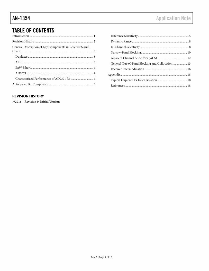
TABLE OF CONTENTS Introduction ...................................................................................... 1 Revision History ............................................................................... 2 General Description of Key Components in Receiver Signal Chain .................................................................................................. 3
Duplexer ........................................................................................ 3 AFE ................................................................................................. 3 SAW Filter ..................................................................................... 4 AD9371 .......................................................................................... 4 Characterized Performance of AD9371 Rx .............................. 4
Anticipated Rx Compliance ............................................................ 5
Reference Sensitivity .....................................................................5 Dynamic Range .............................................................................8 In-Channel Selectivity ..................................................................8 Narrow-Band Blocking .............................................................. 10 Adjacent Channel Selectivity (ACS) ........................................ 12 General Out-of-Band Blocking and Collocation ................... 13 Receiver Intermodulation ......................................................... 16
Appendix ......................................................................................... 18 Typical Duplexer Tx to Rx Isolation ........................................ 18 References .................................................................................... 18
REVISION HISTORY 7/2016—Revision 0: Initial Version

Application Note AN-1354
Rev. 0 | Page 3 of 18
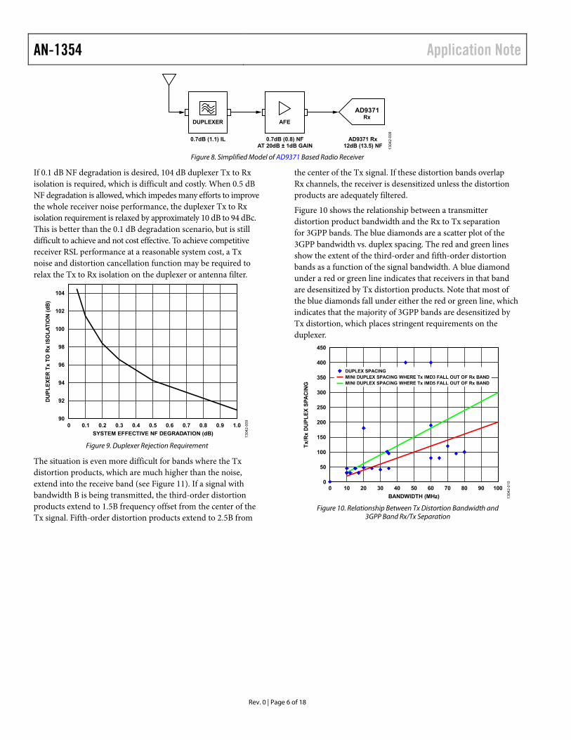
GENERAL DESCRIPTION OF KEY COMPONENTS IN RECEIVER SIGNAL CHAIN DUPLEXER The key function of the duplexer or isolator is to keep transmit energy out of the receiver to prevent desensitization or damage. The duplexer tends to be one of the more costly elements of the receiver and also makes up a significant part of the gross weight and volume. For frequency division duplex (FDD) applications, no duplexer is perfect and, therefore, some part of transmit (Tx) wideband noise spills into the receive (Rx) band and becomes part of the noise budget. If more of the overall noise budget can be allocated to transmit leakage, the duplexer can become smaller, cheaper, and lighter.
In the test setup, the duplexer was modeled as an ideal band-pass filter with 1 dB insertion loss, which was taken into account for the antenna referred power calculation.
AFE An analog front end (AFE) includes a two stage LNA to amplify the weak signal with minimum additive noise so that the AD9371 can digitize signal with reasonable noise contributed to the radio.
Overall system performance at two different AFE gain scenarios (20 dB and 25.5 dB) were discussed and tested.
Table 1. AFE Key Specifications Specification Typical at 2500 MHz Gain 20 dB, 25.5 dB Noise Figure (NF) 0.8 dB Third-Order Intercept Point (IIP3) 6.7 dBm at 20 dB Output 1 dB Compression Point (P1dB) 2 dBm
LPF
AD9371 EVALUATION BOARD
Rx1Rx2
D0 TO D5
50Ω
90°HYBRID HYBRID
ININ
ISO
LNA GAIN
0°
90°
0°
50Ω
ADL5240GAIN = –2.6dB
AVAGO MGA-16×16 DEMO BOARD POPULATED WITH MGA 16×16
ATTENUATOR0dB TO 1dB
AVAGOFBAR
FILTER
AVAGO MGA 63×P8EVALUATION BOARD
LPF
LOGENERATION
ADC
ADC
1304
2-00
4
Figure 4. AFE Detailed Block Diagram and Connection to AD9371

AN-1354 Application Note
Rev. 0 | Page 4 of 18
SAW FILTER The two purposes of the RF filter are to remove as much out-of-band energy as possible, including out-of-band blockers, and to provide additional attenuation of wideband transmit noise and intermodulation products that otherwise degrade receiver performance. Use a differential output SAW filter to match the differential RF input on the AD9371, if possible. The alternative is to use a RF balun. A differential architecture allows higher even-order performance metrics as well as much higher common-mode rejection to local oscillators (LOs), clocks, power supply noise, and other system signals.
For optimal out-of-band performance, it is recommended to insert an RF SAW filter between two LNA stages to improve the out-of-band linearity performance of the whole receiver chain. This brings value to the system by relaxing duplexer out-of-band rejection requirements.
AD9371 The AD9371 is a highly integrated, RF agile transceiver offering dual-channel transmitters and receivers, integrated synthesizers, and digital signal processing functions. The AD9371 delivers a versatile combination of high performance and low power consumption required by 3G/4G micro through macro BTS equipment and can operate in both FDD and TDD applications.
The AD9371 operates from 300 MHz to 6000 MHz covering most of the licensed and unlicensed cellular bands. The AD9371 includes full LO and clock synthesis, supports a JESD204B compliant digital interface over 2 (Rx) or 4 (Tx) lanes, and supports lane speeds of up to 6.144 Gbps.
CHARACTERIZED PERFORMANCE OF AD9371 Rx The analysis in the following sections is based on the characterization data shown in Table 2 and is used to estimate the system performance.
Table 2. Characterized Performance of AD9371 Rx Specification Typical at 2500 MHz NF at Maximum Gain 12 dB Second-Order Intercept Point (IIP2) 63 dBm Third-Order Intercept Point (IIP3) 22 dBm Image Rejection 75 dB Internal LO Phase Noise
At 10 kHz −95 dBc/Hz At 100 kHz −100 dBc/Hz At 1 MHz −123 dBc/Hz At 10 MHz <−140 dBc/Hz
LPF
AD9371 EVALUATION BOARD
Rx1RX2+RX2–
RX1+RX1–
RX_EXT_LO+RX_EXT_LO–
REF_CLK_IN_PREF_CLK_IN_N
GPIO_3P3_0TO
GPIO_3P3_11
GPIO_0TO
GPIO_18
AUXADC_0TO
AUXADC_3
AUXDAC_0TO
AUDAC_9
Rx2 RX_SYNCB_P/NRX_DATA_0P/NRX_DATA_1P/NSYSREF_INP/N
SPI
JESD_INTERRUPTEN_AGCRX_ENABLERESETREF_CLK_IN_PLPF
LOGENERATION
RFSYNTHESIZER
GPIO, AUXADC, AND AUXDACs
12
CLOCKGENERATION
DIGITALPROCESSING
DECIMATION,pFIR, AGC,
DC OFFSET,QEC, TUNING,
OVERLOADINDICATION,
MULTICHIP SYNCADC
ADC
1304
2-00
5
18 4 10
4
Figure 5. AD9371 Internal Block Diagram
Application Note AN-1354
Rev. 0 | Page 5 of 18
ANTICIPATED Rx COMPLIANCE REFERENCE SENSITIVITY Analysis
Figure 7 shows the required reference sensitivity level (RSL) for LTE in a wide area base transceiver station (BTS). The wide area BTS RSL for a 5 MHz carrier bandwidth (BW) corresponds to a −168 dBm/Hz signal density.
With an FRC A1-3 reference measurement channel and a modulation and coding scheme of MCS-4, the 95% throughput can be expected to have approximately −1 dB signal-to-noise ratio (SNR), depending on the link conditions and capabilities of the specific IP implementation. To meet the RSL requirement of the specification, the highest possible overall system NF is 7 dB (−168 dBm/Hz − (−1 dB) − (−174 dBm/Hz) = 7dB). All base station vendors want to achieve better RSL than the 3GPP requirement; therefore, typical system NFs are 2 dB to 3 dB, which allows a 5 dB to 4 dB margin, respectively, to be achieved.
Figure 8 shows a typical simplified block diagram. It gives a 1.8 dB overall antenna referred system NF at the AD9371 band center, 2.0 dB at the band edge in the typical case, and 2.5 dB at the band edge in the worst case. This leaves an approximate 0.5 dB margin for other factors with 2.5 dB typical NF and 3 dB worst-case NF as design targets.
In an FDD system, Rx noise is determined by the receiver NF and by Tx emission leakages into the Rx band. Tx emissions can be noise, distortion, or the sum of the two depending on the Tx to Rx frequency separation of the operating band and the signal bandwidth. The transmitter emission levels depend on the Tx power, the linearity and noise of the transmitter, and the Tx port to antenna port to Rx port rejection of the duplexer.
Digital predistortion (DPD) is necessary in moderate to high Tx power applications and requires a transmitter with a wide synthesis bandwidth, which means that the Tx noise cannot be filtered much prior to the duplexer. With an AD9371 based
transmitter, for example, the in-band noise at the AD9371 output is −151 dBm/Hz with −5 dBm rms output power assuming 12 dB backoff. If the output power at the antenna is 4 carriers at 46 dBm (10 W per carrier), for example, there is a total of 51 dB of gain and the power amplifier (PA) output noise is −99 dBm/Hz.
At a 60 dB adjacent channel leakage ratio (ACLR), the PA distortion that falls into the Rx band for the 46 dBm total transmit power of a 4-carrier antenna output is −87 dBm/Hz. Combined with AD9371 Tx thermal noise, this gives a total of −86.7 dBm/Hz Tx noise plus distortion power density in the Rx band for 3 MHz BW LTE, which is far above the −174 dBm/Hz noise floor, and therefore the noise must be rejected by the duplexer.
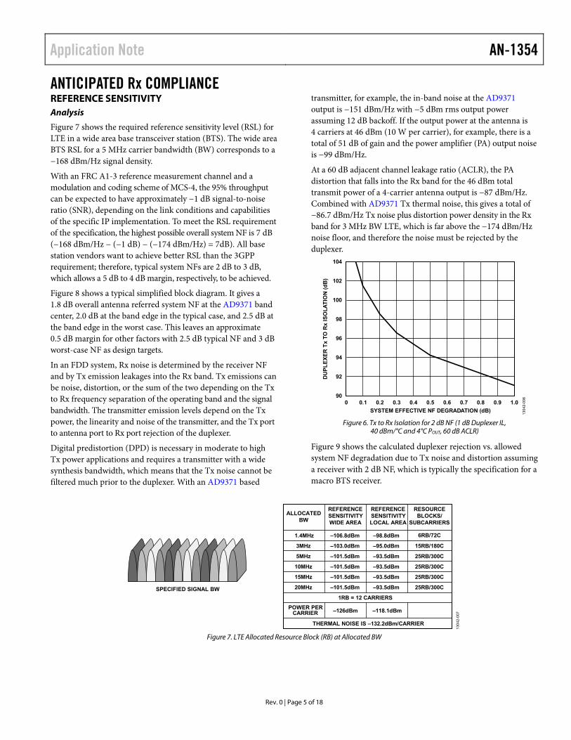
104
102
100
98
96
94
92
0 0.1 0.2 0.3 0.4 0.5SYSTEM EFFECTIVE NF DEGRADATION (dB)
DU
PLEX
ER T
xTO
Rx
ISO
LATI
ON
(dB
)
0.6 0.7 0.8 0.9 1.090
1304
2-00
6
Figure 6. Tx to Rx Isolation for 2 dB NF (1 dB Duplexer IL,
40 dBm/°C and 4°C POUT, 60 dB ACLR)
Figure 9 shows the calculated duplexer rejection vs. allowed system NF degradation due to Tx noise and distortion assuming a receiver with 2 dB NF, which is typically the specification for a macro BTS receiver.
SPECIFIED SIGNAL BW
1.4MHz
15MHz
20MHz
10MHz
5MHz
3MHz
–106.8dBm
–101.5dBm
–101.5dBm
–101.5dBm
–101.5dBm
–103.0dBm
1RB = 12 CARRIERS
ALLOCATEDBW
REFERENCESENSITIVITYWIDE AREA
REFERENCESENSITIVITYLOCAL AREA
6RB/72C
25RB/300C
25RB/300C
25RB/300C
25RB/300C
15RB/180C
RESOURCEBLOCKS/
SUBCARRIERS
–98.8dBm
–93.5dBm
–93.5dBm
–93.5dBm
–93.5dBm
–95.0dBm
POWER PERCARRIER –126dBm –118.1dBm
THERMAL NOISE IS –132.2dBm/CARRIER
1304
2-00
7
Figure 7. LTE Allocated Resource Block (RB) at Allocated BW
AN-1354 Application Note
Rev. 0 | Page 6 of 18
AFEDUPLEXER
0.7dB (1.1) IL 0.7dB (0.8) NFAT 20dB ± 1dB GAIN
AD9371 Rx12dB (13.5) NF 13
042-
008
AD9371Rx
Figure 8. Simplified Model of AD9371 Based Radio Receiver
If 0.1 dB NF degradation is desired, 104 dB duplexer Tx to Rx isolation is required, which is difficult and costly. When 0.5 dB NF degradation is allowed, which impedes many efforts to improve the whole receiver noise performance, the duplexer Tx to Rx isolation requirement is relaxed by approximately 10 dB to 94 dBc. This is better than the 0.1 dB degradation scenario, but is still difficult to achieve and not cost effective. To achieve competitive receiver RSL performance at a reasonable system cost, a Tx noise and distortion cancellation function may be required to relax the Tx to Rx isolation on the duplexer or antenna filter.
104
102
100
98
96
94
92
0 0.1 0.2 0.3 0.4 0.5SYSTEM EFFECTIVE NF DEGRADATION (dB)
DU
PLEX
ER T
xTO
Rx
ISO
LATI
ON
(dB
)
0.6 0.7 0.8 0.9 1.090
1304
2-00
9
Figure 9. Duplexer Rejection Requirement
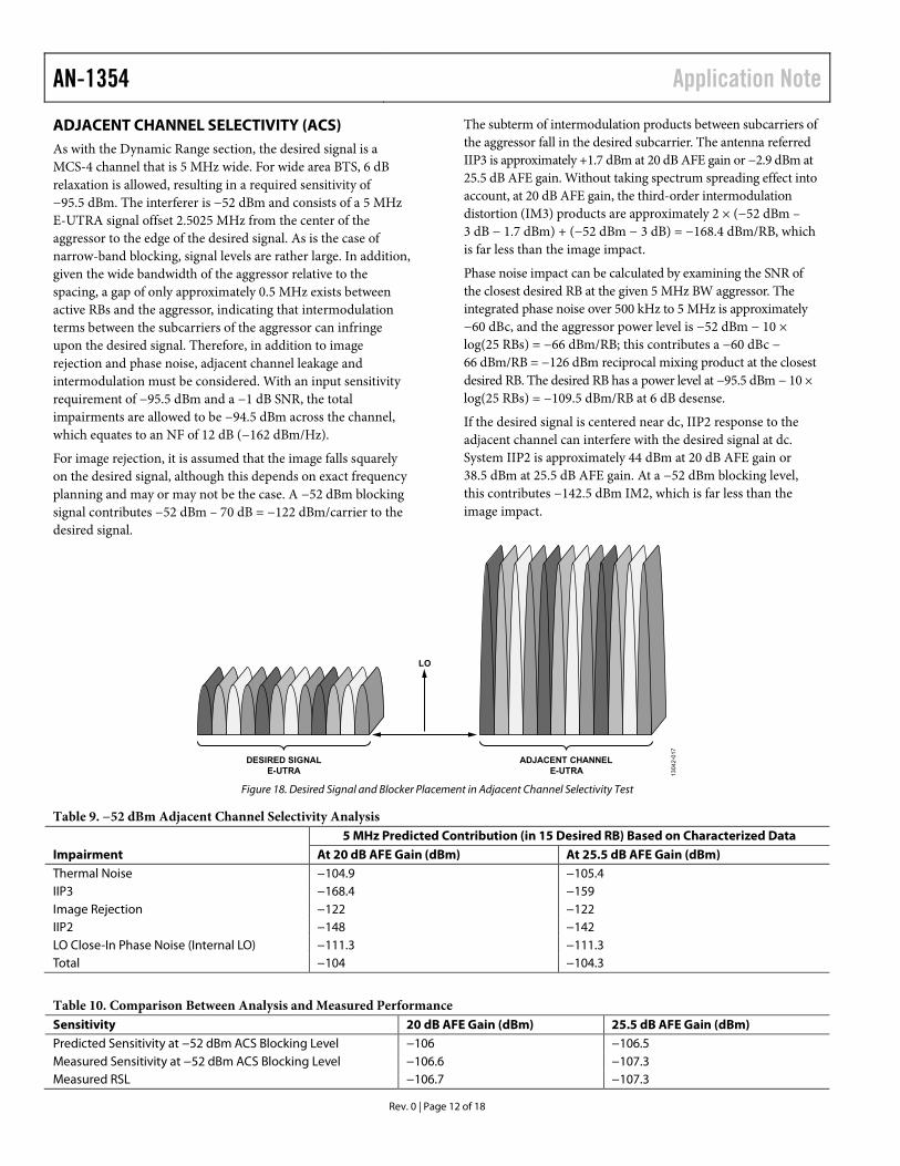
The situation is even more difficult for bands where the Tx distortion products, which are much higher than the noise, extend into the receive band (see Figure 11). If a signal with bandwidth B is being transmitted, the third-order distortion products extend to 1.5B frequency offset from the center of the Tx signal. Fifth-order distortion products extend to 2.5B from
the center of the Tx signal. If these distortion bands overlap Rx channels, the receiver is desensitized unless the distortion products are adequately filtered.
Figure 10 shows the relationship between a transmitter distortion product bandwidth and the Rx to Tx separation for 3GPP bands. The blue diamonds are a scatter plot of the 3GPP bandwidth vs. duplex spacing. The red and green lines show the extent of the third-order and fifth-order distortion bands as a function of the signal bandwidth. A blue diamond under a red or green line indicates that receivers in that band are desensitized by Tx distortion products. Note that most of the blue diamonds fall under either the red or green line, which indicates that the majority of 3GPP bands are desensitized by Tx distortion, which places stringent requirements on the duplexer.
0
50
100
150
200
250
300
350
400
450
0 10 20 30 40 50 60 70 80 90 100
Tx/R
x D
UPL
EX S
PAC
ING
BANDWIDTH (MHz)
DUPLEX SPACINGMINI DUPLEX SPACING WHERE Tx IMD3 FALL OUT OF Rx BANDMINI DUPLEX SPACING WHERE Tx IMD5 FALL OUT OF Rx BAND
1304
2-01
0
Figure 10. Relationship Between Tx Distortion Bandwidth and
3GPP Band Rx/Tx Separation

Application Note AN-1354
Rev. 0 | Page 7 of 18
THIRD-ORDER DISTORTION BAND
B
FIFTH-ORDER DISTORTION BAND
BASE STATION Rx BAND BASE STATION Tx BAND
FDUPLEX
1304
2-01
1
Figure 11. Tx Distortion Bands and Duplex Spacing
Table 3. Reference Sensitivity Analysis Specification 5 MHz Estimate 1.4 MHz Estimate Achievable NF 2.81 dB 2.81 dB RSL −105.7 dBm/25 RBs −111.8 dBm/6 RBs IIP3 −0.55 dBm −0.55 dBm IIP2 +40 dBm +40 dBm P1dB −33.5 dBm (maximum gain) −33.5 dBm (maximum gain)
Test Results
Lab measurements are summarized in this section. Note that the ADL5240 amplifier was used instead of a second stage LNA; therefore, AFE NF was slightly worse than modeled. Sensitivity information is extrapolated from measured SNR. The NF or sensitivity does not take the Tx leakage into account.
–130
–125
–120
–115
–110
–105
–100
–95
–90UMTS
RSL
(dB
m)
5MHz 25RBs LTE
20dB NET GAIN25.5dB NET GAIN
1304
2-01
2
Figure 12. WCDAM and LTE Measured RSL at 2 AFE Gain
Comparison Between Analysis and Measured Performance
0
0.5
1.0
1.5
2.0
2.5
SYST
EM N
F (d
B)
3.0
3.5
EXTRAPOLATEDFROM UMTSSIGNAL EVM
MEASUREMENTS
EXTRAPOLATEDFROM
5MHz 25RBsLTE EVM
MEASUREMENTS
FROM CWTONE SNR
MEASUREMENTS
PREDICTEDFROM CASCADEDRECEIVER CHAIN
TYPICALPARAMETERS
20dB NET GAIN25.5dB NET GAIN
1304
2-01
3
Figure 13. System NF Measured with Different Methods
The measured system NF is close to the analysis results (0.5 dB maximum). The system NF from both analysis and measurements meet the targeted 3 dB.

AN-1354 Application Note
Rev. 0 | Page 8 of 18
DYNAMIC RANGE Analysis
For dynamic range testing, as shown in the 3GPP TS 36.104 document, a 5 MHz desired signal of −70.2 dBm is applied based on MCS-9. The additive white Gaussian noise (AWGN) interfering signal is −82.5 dBm. MCS-9 has a 95% throughput corner around 10 dB of SNR. If additional impairments do not degrade SNR greater than 2.3 dB, the dynamic range performance is satisfied. Because the desired signal is the dominant signal, most reasonable implementations do not cause any self-blocking impairments. This is more of a baseband specification than a radio specification and therefore does not challenge receiver performance. For narrow-band signals, the relationship between signal and interference remains approximately the same. Therefore, performance across the different spectral allocations remains the same.
Test Result
Dynamic range was not tested, only analyzed.
IN-CHANNEL SELECTIVITY Analysis
For wide area BTS, in-channel selectivity for a 5 MHz E-UTRA signal is tested with one signal of 15 resource blocks (RBs) (MSC-4) at −100 dBm and an adjacent 10 RBs interference at −81 dBm to fill out the remaining 5 MHz E-UTRA channel.
The 5 MHz E-UTRA signal at −100 dBm corresponds to −100 dBm − 10 × log(15 RB) = −111.8 dBm/RB for the desired RB power level, and −81 dBm – 10 × log(10 RB) = −91 dBm/RB for interference RB power level.
As noted previously, an MSC-4 signal has a corner SNR at approximately −1 dB, below which throughput falls below 95%.
Despite the close proximity of the interferer, neither absolute power nor the power disparity between the two is significant enough to present a challenge for the radio. Typical radio performance for specifications such as image rejection, IIP2, and IIP3 do not contribute to the performance of this test because the interference signal power is very low.
LO close-in phase noise has the greatest impact on the RB next to dc. The reciprocal mixing products between LO phase noise at the 100 Hz to 360 kHz range, and the interference RB falls into the desired RB. The integrated phase noise (phase jitter) of the AD9371 internal LO is approximately −33 dBc; this contributes −91 dBm + (−33) = −124 dBm, which gives approximately −111.8 dBm − (−124 dBm) = 12.2 dB SNR for the closest desired RB (next to dc).
The 1/f noise of the baseband signal chain (0 Hz to a few 10s of kHz) may contribute more than LO phase noise. To remove 1/f noise, the AD9371 employs a digital notch filter. The notch filter BW is programmable; a wider notch filter helps to remove wide range 1/f noise, and therefore it is helpful at lower signal levels. The notch filter also cuts off part of the desired signal energy; therefore, a wider notch filter can degrade SNR at higher signal levels. An optimal notch filter BW can be chosen to achieve balanced performance for small and large signal conditions.
In-channel selectivity for a 1.4 MHz E-UTRA signal is tested with one signal of 3 RBs (MSC-4) at −98.9 dBm and an adjacent 3 RBs at −79 dBm to fill out the remaining E-UTRA channel. Using the same constraints discussed previously, the required performance is shown in Table 4 and Table 5. As with the wider bandwidth configuration, none of the requirements are a challenge for the AD9371.
In Table 5, the lab measured data for ICS performance is quite close to analyzed performance for each of the key measurements.
DESIRED SIGNAL
INTERFERENCE RB
LO PHASE NOISE
DESIRED RB
IN-CHANNEL BLOCKER
DC
130
42
-01
4
Figure 14. In-Channel Selectivity
Application Note AN-1354
Rev. 0 | Page 9 of 18
Table 4. −81 dBm at 10 RB In-Channel Selectivity Analysis 5 MHz Predicted Contribution (in 15 Desired RB) Based on Characterized Data Impairment At 20 dB AFE Gain (dBm) At 25.5 dB AFE Gain (dBm) Thermal Noise −107.1 −107.7 IIP3 −246 −237 Image Rejection −151 −151 IIP2 −206 −200 LO Close-In Phase Noise −114.7 −114.7 Notch Filter (×100 Hz Notch BW) −145 −145 Total −106.4 −106.9
Table 5. Test Results and Comparison Between Analysis and Measured Performance Sensitivity 20 dB AFE Gain (dBm) 25.5 dB AFE Gain (dBm) Extrapolated Sensitivity at −1 dB SNR from Measured EVM Data −107.4 −107.9 Standard RSL Specification −101.5 −101.5 Predicted Sensitivity at −1 dB SNR −108.0 −108.5

AN-1354 Application Note
Rev. 0 | Page 10 of 18
NARROW-BAND BLOCKING Analysis
As with the Reference Sensitivity section, the desired signal is a 5 MHz wide MCS-4 channel. For wide area BTS, 6 dB relaxation is allowed, resulting in a required sensitivity of −95.5 dBm. The interferer is a single RB at −49 dBm and appears at an offset frequency based on the equation found in the TS 36.141 document.
This is the offset from the center of the narrow-band blocker to the channel edge of the desired signal, as shown in Figure 17. Given the large nature of this signal, the receiver is susceptible to common impairments including image rejection and phase noise. With an input sensitivity requirement of −95.5 dBm and a −1 dB SNR, the total impairments are allowed to be −94.5 dBm across the channel, which equates to an NF of 13 dB (−161 dBm/Hz).
For image rejection, the resulting aggressor may or may not fall on the desired signal. Assuming that it does, two possibilities can occur. One is that the image falls squarely on a desired resource block. The other possibility is that the image falls partly across two adjacent resource blocks. For this discussion, it is assumed that the image falls squarely on one resource block, but keep in mind that the impairment can involve two adjacent resource blocks. In addition, total throughput is based on all RBs, not just the impaired RB; therefore, this represents a worst-case scenario. A −49 dBm blocking contributes −49 dBm − 70 dB = −119 dBm impairment at 70 dBc image rejection.
When blocking is at the minimum frequency offset from the desired signal, the phase noise impact is the greatest. For a 1.4 MHz case, the phase noise at an offset of 400 kHz to 1.5 MHz affects the SNR of the desired signal. In the 5 MHz carrier BW case, phase noise at offsets between 600 kHz and 5.1 MHz impact SNR. The integrated phase noise for the AD9371 internal LO in the 400 kHz to 1.5 MHz range is approximately −59 dBc, and approximately −61 dBc in the 600 kHz to 5.1 MHz range. This contributes approximately −108.7 dBm for 1.4 MHz and 3 MHz carrier BWs, and −110 dBm for a 5 MHz carrier BW.
The RB closest to the offender is most affected by close-in phase noise. The frequency offset from the NB blocking center to the desired RB is 400 kHz to 580 kHz for 1.4 MHz BW, or 600 kHz to 780 kHz for 5 MHz BW. The integrated phase noise is approximately −62 dBc over frequency offset from 400 kHz to 580 kHz.
The integrated phase noise contributes approximately −111 dBm/RB for 1.4 MHz carrier BW, or −113 dBm/RB for 5 MHz carrier BW. Because the desired signal level (6 dB higher than RSL) is −108.7 dBm/RB for 1.4 MHz BW, or −109.5 dBm/RB for 5 MHz BW, the phase noise limited SNR for the RB closest to the offender (NB blocking RB) is approximately 3 dB for 1.4 MHz BW or 3.8 dB for 5 MHz BW, which is above −1 dB. For those desired RBs farther away from the offender, the SNR improves as phase noise improves and as frequency offset increases.
–50
–40
–60
–70
–80
–90
–100
–110
–50 0FREQUENCY (MHz)
PHA
SE N
OIS
E (d
BFS
)
50–120
1304
2-01
5
Figure 15. Image Rejection Before Correction on a 5 MHz LTE Signal
–50
–40
–60
–70
–80
–90
–100
–110
–50 0FREQUENCY (MHz)
PHA
SE N
OIS
E (d
BFS
)
50–120
1304
2-11
5
Figure 16. Image Rejection After Correction on a 5 MHz LTE Signal

Application Note AN-1354
Rev. 0 | Page 11 of 18
DESIRED SIGNALNARROW-BAND
BLOCKER 1304
2-01
6
Figure 17. Desired Signal and Blocker Placement for Narrow-Band Blocking Test
Table 6. Phase Noise Contribution Analysis for −49 dBm Narrow-Band Blocking LTE Carrier BW AD9371 Internal LO Phase Noise Impact 1.4 MHz 5 MHz Minimum Frequency Offset from Blocker Center to the Desired RB Being Affected 400 kHz 600 kHz Reciprocal Products on all Allocated RBs due to LO/Clock Close-In Phase Noise −108.7 dBm/15 RB −110 dBm/25 RB Reciprocal Products on Closest RB due to LO/Clock Close-In Phase Noise −111.7 dBm/RB −113.3 dBm/RB
Table 7. −49 dBm Narrow-Band Blocking Analysis 5 MHz Predicted Contribution (in 15 Desired RB) Based on Characterized Data Impairment At 20 dB AFE Gain (dBm) At 25.5dB AFE Gain (dBm) Thermal Noise −105.07 −105.53 IIP3 Not applicable Not applicable Image Rejection −119 −119 IIP2 Not applicable Not applicable LO Close-In Phase Noise −108.72 −110 Total −103.4 −104
Table 8. Comparison Between Analysis and Measured Performance Sensitivity 20 dB AFE Gain (dBm) 25.5 dB AFE Gain (dBm) RSL −106.7 −107.3 Predicted Sensitivity
−1 dB SNR −104.4 −105 Extrapolated Sensitivity at −1 dB SNR from Measured EVM Data −106.1 −106.5 Standard RSL Specification −101.5 −101.5
AN-1354 Application Note
Rev. 0 | Page 12 of 18
ADJACENT CHANNEL SELECTIVITY (ACS) As with the Dynamic Range section, the desired signal is a MCS-4 channel that is 5 MHz wide. For wide area BTS, 6 dB relaxation is allowed, resulting in a required sensitivity of −95.5 dBm. The interferer is −52 dBm and consists of a 5 MHz E-UTRA signal offset 2.5025 MHz from the center of the aggressor to the edge of the desired signal. As is the case of narrow-band blocking, signal levels are rather large. In addition, given the wide bandwidth of the aggressor relative to the spacing, a gap of only approximately 0.5 MHz exists between active RBs and the aggressor, indicating that intermodulation terms between the subcarriers of the aggressor can infringe upon the desired signal. Therefore, in addition to image rejection and phase noise, adjacent channel leakage and intermodulation must be considered. With an input sensitivity requirement of −95.5 dBm and a −1 dB SNR, the total impairments are allowed to be −94.5 dBm across the channel, which equates to an NF of 12 dB (−162 dBm/Hz).
For image rejection, it is assumed that the image falls squarely on the desired signal, although this depends on exact frequency planning and may or may not be the case. A −52 dBm blocking signal contributes −52 dBm – 70 dB = −122 dBm/carrier to the desired signal.
The subterm of intermodulation products between subcarriers of the aggressor fall in the desired subcarrier. The antenna referred IIP3 is approximately +1.7 dBm at 20 dB AFE gain or −2.9 dBm at 25.5 dB AFE gain. Without taking spectrum spreading effect into account, at 20 dB AFE gain, the third-order intermodulation distortion (IM3) products are approximately 2 × (−52 dBm – 3 dB − 1.7 dBm) + (−52 dBm − 3 dB) = −168.4 dBm/RB, which is far less than the image impact.
Phase noise impact can be calculated by examining the SNR of the closest desired RB at the given 5 MHz BW aggressor. The integrated phase noise over 500 kHz to 5 MHz is approximately −60 dBc, and the aggressor power level is −52 dBm − 10 × log(25 RBs) = −66 dBm/RB; this contributes a −60 dBc − 66 dBm/RB = −126 dBm reciprocal mixing product at the closest desired RB. The desired RB has a power level at −95.5 dBm − 10 × log(25 RBs) = −109.5 dBm/RB at 6 dB desense.
If the desired signal is centered near dc, IIP2 response to the adjacent channel can interfere with the desired signal at dc. System IIP2 is approximately 44 dBm at 20 dB AFE gain or 38.5 dBm at 25.5 dB AFE gain. At a −52 dBm blocking level, this contributes −142.5 dBm IM2, which is far less than the image impact.
DESIRED SIGNALE-UTRA
LO
ADJACENT CHANNELE-UTRA 13
042-
017
Figure 18. Desired Signal and Blocker Placement in Adjacent Channel Selectivity Test
Table 9. −52 dBm Adjacent Channel Selectivity Analysis 5 MHz Predicted Contribution (in 15 Desired RB) Based on Characterized Data Impairment At 20 dB AFE Gain (dBm) At 25.5 dB AFE Gain (dBm) Thermal Noise −104.9 −105.4 IIP3 −168.4 −159 Image Rejection −122 −122 IIP2 −148 −142 LO Close-In Phase Noise (Internal LO) −111.3 −111.3 Total −104 −104.3
Table 10. Comparison Between Analysis and Measured Performance Sensitivity 20 dB AFE Gain (dBm) 25.5 dB AFE Gain (dBm) Predicted Sensitivity at −52 dBm ACS Blocking Level −106 −106.5 Measured Sensitivity at −52 dBm ACS Blocking Level −106.6 −107.3 Measured RSL −106.7 −107.3

Application Note AN-1354
Rev. 0 | Page 13 of 18
GENERAL OUT-OF-BAND BLOCKING AND COLLOCATION General Out-of-Band Blocking
General blocking requirements for LTE require tolerance of a −15 dBm continuous wave (CW) tone a certain distance outside of the desired band. This can be anywhere between 10 MHz and 20 MHz, depending on the band, and extends from 1 MHz to 12.750 GHz. In collocation scenarios, the blocking level is 16 dBm.
The AD9371 internal architecture provides approximately 20 dB rejection at 200 MHz offset from its pass-band edge, over 40 dB at 500 MHz offset, and over 50 dB at the far-out band, which is beyond the first Nyquist zone (−614.4 MHz to +614.4 MHz) of the internal Σ-Δ ADC.
The AD9371 internal architecture in part defines rejection performance of the duplexer, or antenna filter for time division duplex (TDD), and other RF filters. Total rejection of this signal by the duplexer and other filters reduces the level to a point where it does not disrupt receiver performance. This reduction is important for general blocking, but specifically important for collocation situations where the out-of-band signals may be quite large. There are several ways that these signals can disrupt performance if not filtered properly. First, the linearity of the front end (LNA and other RF amplifiers) can be compromised. Second, out-of-band signals can alias within the ADC and show up as in-band blockers. It is also possible that out-of-band signals can overdrive the ADC. Finally, in-band signals can potentially desensitize the performance of the receiver.
For IF sampling architectures, these out-of-band signals must be sufficiently filtered to a level equal to or less than thermal noise levels to prevent degrading receiver sensitivity too much. For instance, total filtering must be equal to or better than +16 dBm – (2 dB − 174 dBm/Hz + 10 × log(4.5 MHz)) = 122 dB, which corresponds to 3 dB desensitization for achieved RSL at 2 dB system NF.
In an IF sampling receiver, the filtering is distributed between RF and IF to achieve the desired filtering requirement. Specifically, this requires an RF filter in front of the mixer to prevent signals and noise on the other side of the LO from showing up in-band with the desired mixer image. For ZIF architectures, there is no out-of-band image in theory, though on silicon, the AD9371 provides limited rejection (>50 dB), as stated previously, for high-order images (beyond the first Nyquist frequency range). Therefore, this RF filter can be moved closer to the antenna, improving out-of-band protection for all but particularly the second stage LNA; therefore, the
entire out-of-band linearity of the radio is improved. There may be less than 1/10 dB reduction of noise figure with the filter closer to the antenna. In the sweep shown in Figure 20, desensitization is plotted against frequency. Far out of band, the limitation is from LNA linearity and not by noise associated with other phenomenon such as phase noise or converter noise floor. Including an RF filter between the first LNA and second LNA reduces out-of-band linearity issues and improves overall system performance due to this limitation. Including an RF filter in between two LNA stages is not possible with an IF sampling architecture without more of an impact on NF.
As shown in Figure 20, blockers immediately outside the band of interest are very difficult to filter. Blockers immediately outside of the band of interest include transmit leakage as well as unrelated sources. Duplexers can be increased in complexity to help but do not eliminate these problems at a cost. Similarly, SAW filters do not eliminate these signals entirely either. A typical IF sampling architecture must tolerate signals as high as perhaps −35 dBm across the entire band that might alias from out-of-band sources. The blockers must be attenuated with IF filters below the spurious level of the amplifier and ADC combined to prevent disruption of the receiver. Other signals must be filtered as well, including LO leakage and undesired mixer images. The result is typically a high-order IF filter with an insertion loss of approximately 6 db to 12 dB, depending on what the transition response needs to be. A ZIF architecture eliminates nearly all of these concerns. With a ZIF architecture, the primary signals are those of interest and their products. These products are typically mitigated by various analog and digital techniques. Because of the general low-pass characteristics of the on-chip AAF filter and the Σ-Δ modulator used to digitize the signal, out-of-band signals are naturally rejected by the signal transfer function of the Σ-Δ converter. Combined with a high sample rate, the ZIF architecture using a Σ-Δ converter increases tolerance to out-of-band content, especially far-out bands, and the filtering burden is lessened. This is highlighted in Figure 20 by the increasing input level required to desensitize the receiver right outside of the band of interest. In summary, tolerance to out-of-band desensitization is higher than that of in-band desensitization.
In the traditional IF sampling architecture with pipeline ADCs, filters must deal with both close-in out-of-band blocking and far out ones; therefore, the insertion loss and cost is high. In contrast, the AD9371 has good immunity to far-out blocking and, therefore, the RF filter(s) can be optimized for close-in rejection.

AN-1354 Application Note
Rev. 0 | Page 14 of 18
Special Out-of-Band Blocking for LTE-TDD
LTE-TDD operators may demand out-of-band tolerance that can tolerate certain blocking power level (higher than in-band blocking power level) at a smaller blocker signal to desired signal frequency offset (smaller than the standard out-of-band blocking scenario), for example, a −35 dBm blocking level at a 5 MHz offset from the desired band edge. Because the transition band (5 MHz) is so small relative to the pass-band frequency, even a cavity filter cannot accomplish much at reasonable cost; therefore, the situation is nearly the same as the in-band blocking scenario.
With an AFE gain of 20 dB and 2 dB antenna to LNA input loss, the AD9371 automatic gain control (AGC) starts to reduce gain for signals at this level. Considering a peak to average ratio (PAR) for a 5 MHz LTE signal of approximately 7.2 dB, the peak input power for the AD9371 is approximately −35 dBm − 2 dB + 20 dB + 7.2 dB = −10 dBm. At −13 dBm ADC equivalent full-scale power and 3 dB headroom for the AGC, −10 dBm − (−13 dBm − 3 dB) = 6 dB of attenuation must be used within the AD9371 so that the effective NF is degraded.
Phase noise is an issue because the blocking level is high. In this special scenario, the image is not an issue. IM2 can be an issue for the carriers around dc.
The impairments are shown in Table 11.
Table 11. −35 dBm Out-of-Band Blocking Analysis
Impairment 20 dB AFE Gain (dBm)
25.5 dB AFE Gain (dBm)
Thermal Noise −103.4 −103.2 IM3 −124.6 −125 Image Not applicable Not applicable Phase Noise −107 −107 IM2 −126 −126.5 Total −101.8 101.7
Table 12. Comparison Between Analysis and Measured Performance
General In-Band Blocking Test 20 dB AFE Gain (dBm)
25.5 dB AFE Gain (dBm)
Predicted Sensitivity at −35 dBm In-Band Blocking Level
−102.8 −102.7
Measured Sensitivity at −35 dBm In-Band Blocking Level
−101.5 −101.5
Measured RSL −104.5 −104.9
Application Note AN-1354
Rev. 0 | Page 15 of 18
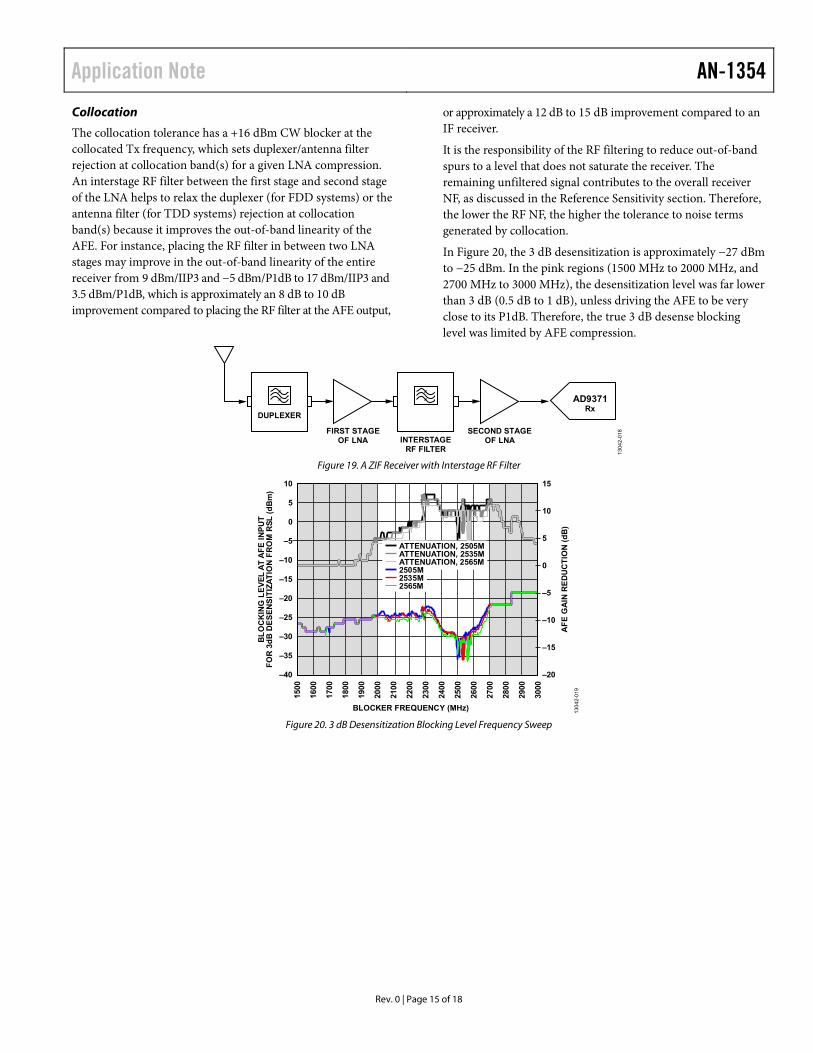
Collocation
The collocation tolerance has a +16 dBm CW blocker at the collocated Tx frequency, which sets duplexer/antenna filter rejection at collocation band(s) for a given LNA compression. An interstage RF filter between the first stage and second stage of the LNA helps to relax the duplexer (for FDD systems) or the antenna filter (for TDD systems) rejection at collocation band(s) because it improves the out-of-band linearity of the AFE. For instance, placing the RF filter in between two LNA stages may improve in the out-of-band linearity of the entire receiver from 9 dBm/IIP3 and −5 dBm/P1dB to 17 dBm/IIP3 and 3.5 dBm/P1dB, which is approximately an 8 dB to 10 dB improvement compared to placing the RF filter at the AFE output,
or approximately a 12 dB to 15 dB improvement compared to an IF receiver.
It is the responsibility of the RF filtering to reduce out-of-band spurs to a level that does not saturate the receiver. The remaining unfiltered signal contributes to the overall receiver NF, as discussed in the Reference Sensitivity section. Therefore, the lower the RF NF, the higher the tolerance to noise terms generated by collocation.
In Figure 20, the 3 dB desensitization is approximately −27 dBm to −25 dBm. In the pink regions (1500 MHz to 2000 MHz, and 2700 MHz to 3000 MHz), the desensitization level was far lower than 3 dB (0.5 dB to 1 dB), unless driving the AFE to be very close to its P1dB. Therefore, the true 3 dB desense blocking level was limited by AFE compression.
FIRST STAGEOF LNA
DUPLEXER
1304
2-01
8
INTERSTAGERF FILTER
SECOND STAGEOF LNA
AD9371Rx
Figure 19. A ZIF Receiver with Interstage RF Filter
–20
–15
–10
–5
0
5
10
15
–40
–35
–30
–25
–20
BLOCKER FREQUENCY (MHz)
–15
–10
–5
0
5
10
1500
1600
1700
1800
1900
2000
2100
2200
BLO
CK
ING
LEV
ELAT
AFE
INPU
TFO
R 3
dB D
ESEN
SITI
ZATI
ON
FR
OM
RSL
(dB
m)
AFE
GA
IN R
EDU
CTI
ON
(dB
)
2300
2400
2500
2600
2700
2800
2900
3000
2505M2535M2565M
ATTENUATION, 2505MATTENUATION, 2535MATTENUATION, 2565M
1304
2-01
9
Figure 20. 3 dB Desensitization Blocking Level Frequency Sweep
AN-1354 Application Note
Rev. 0 | Page 16 of 18
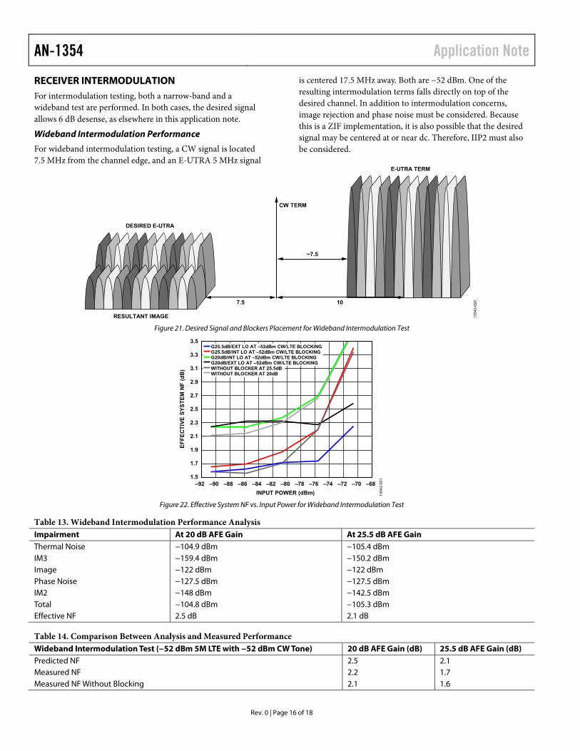
RECEIVER INTERMODULATION For intermodulation testing, both a narrow-band and a wideband test are performed. In both cases, the desired signal allows 6 dB desense, as elsewhere in this application note.
Wideband Intermodulation Performance
For wideband intermodulation testing, a CW signal is located 7.5 MHz from the channel edge, and an E-UTRA 5 MHz signal
is centered 17.5 MHz away. Both are −52 dBm. One of the resulting intermodulation terms falls directly on top of the desired channel. In addition to intermodulation concerns, image rejection and phase noise must be considered. Because this is a ZIF implementation, it is also possible that the desired signal may be centered at or near dc. Therefore, IIP2 must also be considered.
RESULTANT IMAGE
DESIRED E-UTRA
E-UTRA TERM
CW TERM
7.5 10
~7.5
1304
2-02
0
Figure 21. Desired Signal and Blockers Placement for Wideband Intermodulation Test
1.5
1.7
1.9
2.1
2.3
2.5
–92 –90 –88 –86 –84 –82 –80INPUT POWER (dBm)
EFFE
CTI
VE S
YSTE
M N
F (d
B)
–78 –76 –74 –72 –70 –68
G25.5dB/EXT LO AT –52dBm CW/LTE BLOCKINGG25.5dB/INT LO AT –52dBm CW/LTE BLOCKINGG20dB/INT LO AT –52dBm CW/LTE BLOCKINGG20dB/EXT LO AT –52dBm CW/LTE BLOCKINGWITHOUT BLOCKER AT 25.5dBWITHOUT BLOCKER AT 20dB
1304
2-02
1
2.7
2.9
3.1
3.3
3.5
Figure 22. Effective System NF vs. Input Power for Wideband Intermodulation Test
Table 13. Wideband Intermodulation Performance Analysis Impairment At 20 dB AFE Gain At 25.5 dB AFE Gain Thermal Noise −104.9 dBm −105.4 dBm IM3 −159.4 dBm −150.2 dBm Image −122 dBm −122 dBm Phase Noise −127.5 dBm −127.5 dBm IM2 −148 dBm −142.5 dBm Total −104.8 dBm −105.3 dBm Effective NF 2.5 dB 2.1 dB
Table 14. Comparison Between Analysis and Measured Performance Wideband Intermodulation Test (−52 dBm 5M LTE with −52 dBm CW Tone) 20 dB AFE Gain (dB) 25.5 dB AFE Gain (dB) Predicted NF 2.5 2.1 Measured NF 2.2 1.7 Measured NF Without Blocking 2.1 1.6
Application Note AN-1354
Rev. 0 | Page 17 of 18
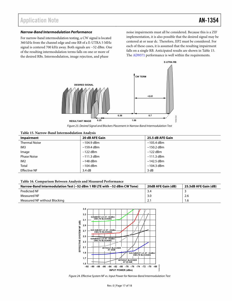
Narrow-Band Intermodulation Performance
For narrow-band intermodulation testing, a CW signal is located 360 kHz from the channel edge and one RB of a E-UTRA 5 MHz signal is centered 700 kHz away. Both signals are −52 dBm. One of the resulting intermodulation terms falls on one or more of the desired RBs. Intermodulation, image rejection, and phase
noise impairments must all be considered. Because this is a ZIF implementation, it is also possible that the desired signal may be centered at or near dc. Therefore, IIP2 must be considered. For each of these cases, it is assumed that the resulting impairment falls on a single RB. Anticipated results are shown in Table 15. The AD9371 performance is well within the requirements.
RESULTANT IMAGE
DESIRED SIGNAL
E-UTRA RB
CW TERM
0.36
0.25
0.7
~0.61
1.06
1304
2-02
2
Figure 23. Desired Signal and Blockers Placement in Narrow-Band Intermodulation Test
Table 15. Narrow-Band Intermodulation Analysis Impairment 20 dB AFE Gain 25.5 dB AFE Gain Thermal Noise −104.9 dBm −105.4 dBm IM3 −159.4 dBm −150.2 dBm Image −122 dBm −122 dBm Phase Noise −111.3 dBm −111.3 dBm IM2 −148 dBm −142.5 dBm Total −104 dBm −104.3 dBm Effective NF 3.4 dB 3 dB
Table 16. Comparison Between Analysis and Measured Performance Narrow-Band Intermodulation Test (−52 dBm 1 RB LTE with −52 dBm CW Tone) 20dB AFE Gain (dB) 25.5dB AFE Gain (dB) Predicted NF 3.4 3 Measured NF 3.0 2.6 Measured NF without Blocking 2.1 1.6
1.5
1.7
1.9
2.1
2.3
2.7
2.9
3.1
3.3
3.5
2.5
–92 –90 –88 –86 –84 –82 –80INPUT POWER (dBm)
EFFE
CTI
VE S
YSTE
M N
F (d
B)
–78 –76 –74 –72 –70 –68
1304
2-02
3
G20dB/INT LO AT –52dBmCW/LTE BLOCKING
G25.5dB/INT LO AT –52dBmCW/LTE BLOCKING
G20dB/EXT LO AT –52dBmCW/LTE BLOCKING
WITHOUT BLOCKERAT 20dB
G25.5dB/EXT LO AT –52dBmCW/LTE BLOCKING
WITHOUT BLOCKERAT 25.5dB
Figure 24. Effective System NF vs. Input Power for Narrow-Band Intermodulation Test
AN-1354 Application Note
Rev. 0 | Page 18 of 18
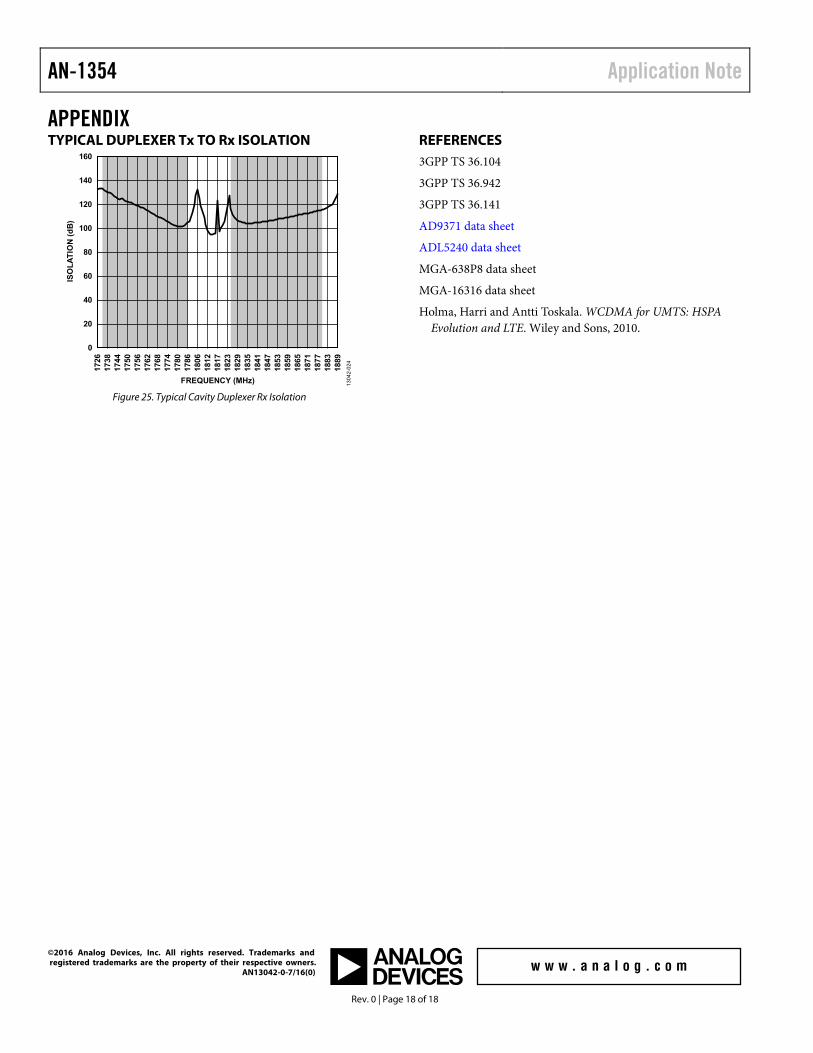
APPENDIX TYPICAL DUPLEXER Tx TO Rx ISOLATION
0
20
40
60
80
100
120
140
160
1726
1738
1744
1750
1756
1762
1768
1774
1780
1786
1806
1812
1817
1823
1829
1835
1841
1847
1853
1859
1865
1871
1877
1883
1889
ISO
LATI
ON
(dB
)
FREQUENCY (MHz) 1304
2-02
4
Figure 25. Typical Cavity Duplexer Rx Isolation
REFERENCES 3GPP TS 36.104
3GPP TS 36.942
3GPP TS 36.141
AD9371 data sheet
ADL5240 data sheet
MGA-638P8 data sheet
MGA-16316 data sheet
Holma, Harri and Antti Toskala. WCDMA for UMTS: HSPA Evolution and LTE. Wiley and Sons, 2010.
©2016 Analog Devices, Inc. All rights reserved. Trademarks and registered trademarks are the property of their respective owners. AN13042-0-7/16(0)