ADF7030-1 Software Reference Manual (Rev. A) Software Reference Manual UG-1002...
81
ADF7030-1 Software Reference Manual UG-1002 One Technology Way • P.O. Box 9106 • Norwood, MA 02062-9106, U.S.A. • Tel: 781.329.4700 • Fax: 781.461.3113 • www.analog.com ADF7030-1 Software Reference Manual PLEASE SEE THE LAST PAGE FOR AN IMPORTANT WARNING AND LEGAL TERMS AND CONDITIONS. Rev. A | Page 1 of 81 SCOPE This manual provides a detailed description of how to control the ADF7030-1 transceiver from the host microcontroller. It is intended as a resource for the firmware engineer developing host microcontroller firmware to communicate with the ADF7030-1. ABOUT THE ADF7030-1 The ADF7030-1 is a low power, high performance, integrated radio transceiver supporting narrow-band and wideband operation in the <1 GHz industrial, scientific, and medical (ISM) bands. The ADF7030-1 features an on-chip ARM® Cortex®-M0 processor that performs radio control and packet management. FUNCTIONAL BLOCK DIAGRAM 14686-001 RECEIVER DIGITAL BASEBAND SYNTHESIZER TRANSMITTER ROM INTERRUPT CONTROLLER SPI SLAVE CONFIGURABLE GPIOs LNA PA PA ARM ® CORTEX ® -M0 RAM TCXO BUFFER LDOx ADF7030-1 26MHz OSC 32kHz OSC TEMPERATURE SENSOR 26kHz RC OSC PAOUT2 PAOUT1 LNAIN1 LNAIN2 CREGx HFXTALN HFXTALP GPIO6 GPIO7 SPI GPIOx NOTES 1. CREGx, GPIOx, AND SPI CONTAIN MULTIPLE PINS. Figure 1. ADF7030-1 Functional Block Diagram
Transcript of ADF7030-1 Software Reference Manual (Rev. A) Software Reference Manual UG-1002...
ADF7030-1 Software Reference Manual UG-1002
One Technology Way • P.O. Box 9106 • Norwood, MA 02062-9106, U.S.A. • Tel: 781.329.4700 • Fax: 781.461.3113 • www.analog.com
ADF7030-1 Software Reference Manual
PLEASE SEE THE LAST PAGE FOR AN IMPORTANT WARNING AND LEGAL TERMS AND CONDITIONS. Rev. A | Page 1 of 81
SCOPE This manual provides a detailed description of how to control the ADF7030-1 transceiver from the host microcontroller. It is intended as a resource for the firmware engineer developing host microcontroller firmware to communicate with the ADF7030-1.
ABOUT THE ADF7030-1 The ADF7030-1 is a low power, high performance, integrated radio transceiver supporting narrow-band and wideband operation in the <1 GHz industrial, scientific, and medical (ISM) bands. The ADF7030-1 features an on-chip ARM® Cortex®-M0 processor that performs radio control and packet management.
FUNCTIONAL BLOCK DIAGRAM
1468
6-00
1
RECEIVER
DIGITALBASEBAND
SYNTHESIZER
TRANSMITTER
ROM
INTERRUPTCONTROLLER
SPISLAVE
CONFIGURABLEGPIOs
LNA
PA
PA
ARM®CORTEX®-M0
RAM
TCXOBUFFERLDOx
ADF7030-126MHz OSC
32kHzOSC
TEMPERATURESENSOR
26kHzRC OSC
PAOUT2
PAOUT1
LNAIN1LNAIN2
CREGx HFXTALN HFXTALP GPIO6 GPIO7
SPI
GPIOx
NOTES1. CREGx, GPIOx, AND SPI CONTAIN MULTIPLE PINS.
Figure 1. ADF7030-1 Functional Block Diagram

UG-1002 ADF7030-1 Software Reference Manual
Rev. A | Page 2 of 81
TABLE OF CONTENTS Scope .................................................................................................. 1 About the ADF7030-1 ...................................................................... 1 Functional Block Diagram .............................................................. 1 Revision History ............................................................................... 4 Introduction ...................................................................................... 5
ADF7030-1 Operation ................................................................. 5 ADF7030-1 Memory Architecture ............................................. 5
Development Support ...................................................................... 7 Design Package ............................................................................. 7 Documentation ............................................................................. 7 Evaluation Kits .............................................................................. 7 Evaluation Software...................................................................... 7
ADF7030-1 State Machine .............................................................. 8 Introduction .................................................................................. 8 ADF7030-1 States ......................................................................... 8 State Transition Timing ............................................................. 11
ADF7030-1 SPI ............................................................................... 12 Introduction ................................................................................ 12 SPI Pins ........................................................................................ 12 Host Initialization of ADF7030-1 SPI...................................... 12 SPI Transactions ......................................................................... 13
ADF7030-1 SPI Communication ................................................. 14 Command Byte ........................................................................... 14 Radio Commands ....................................................................... 14 Radio Commands for External Hardware Triggered Transitions ................................................................................... 16 Radio Command for a System Reset ....................................... 17
Accessing the ADF7030-1 Memory ............................................. 18 Introducton ................................................................................. 18 Summary and Recommendations ............................................ 18 Format of Memory Access Command .................................... 18 Configuring the Pointers for Pointer Based Accesses ........... 19
Configuring the ADF7030-1 ......................................................... 20 Initial Configuration .................................................................. 20 Modifying Configuration at Run Time ................................... 20
Applying the ADF7030-1 Configuration File ............................. 22 ADF7030-1 Configuration File Format ................................... 22
ADF7030-1 Calibration ................................................................. 24 Calibration Guidelines ............................................................... 24 How to Run the Radio Calibration .......................................... 24
Restoring Saved Calibration Results to the ADF7030-1 ....... 25 Temperature Sensor ....................................................................... 26
Example Conversion .................................................................. 26 Transmitting and Receiving Packets ............................................ 27
Overview ..................................................................................... 27 Packet Memory ........................................................................... 27 Packet Formats ............................................................................ 27 Generic Packet Format .............................................................. 28 IEEE802.15.4g Packet Format .................................................. 33 Automatic Frequency Control (AFC) Reporting ................... 36 Rolling Buffers Mode ................................................................. 36 Autoturnaround ......................................................................... 37 Modulation Modes and Line Encoding .................................. 37 External PA and LNA Control .................................................. 39 Test Modes ................................................................................... 39
RSSI, CCA, and Autoturnaround ................................................. 41 RSSI During Packet Reception ................................................. 41 Clear Channel Assessment (CCA) ........................................... 41 CCA Detection Time ................................................................. 41 RSSI Offset Calibration ............................................................. 42
Low Power Modes .......................................................................... 43 PHY_SLEEP ................................................................................ 43 Smart Wake-Up Mode (SWM) ................................................. 44
ADF7030-1 Interrupts ................................................................... 45 Rx and Tx Packet Related Events ............................................. 45 State Machine Events ................................................................. 45 Rolling Buffer Events ................................................................. 45 Clearing Interrupts ..................................................................... 45 Mapping Interrupt Outputs onto GPIOs ................................ 45
GPIO ................................................................................................ 46 General......................................................................................... 46 Interrupt Outputs ....................................................................... 46 Interrupt Inputs .......................................................................... 46 Using External PA or LNA ........................................................ 46
Host to ADF7030-1 Memory Access Modes .............................. 47 Note on Endianness ................................................................... 47 Modes ........................................................................................... 47
Host to ADF7030-1 Message Sequence Charts .......................... 52 Writing the ADF7030-1 Radio Profile from Power-On ........ 52 Transmitting a Single Packet from Power-Off ....................... 53

ADF7030-1 Software Reference Manual UG-1002
Rev. A | Page 3 of 81
Receiving a Single Packet from Power-Off .............................. 54 Calibration Firmware Module, Host Saving ADF7030-1 Calibration Results ...................................................................... 55 Rx Immediately Following Calibration .................................... 55 Rx with Cached Calibration Data ............................................. 56
Register Summary: ADF7030-1 .................................................... 57 Register Details: ADF7030-1 ......................................................... 61
State Machine Wake Source ....................................................... 61 State Machine Command Triggered by IRQ_IN0 Register ... 61 State Machine Command Triggered by IRQ_IN1 Register ... 61 State Machine Control for Calibration ..................................... 61 Reference Clock Configuration Register ................................. 61 RF Channel Frequency Register ................................................ 62 Packet Handler Configuration Register ................................... 62 Radio Mode Configuration Register ........................................ 62 Tx Configuration 0 Register ...................................................... 63 Tx Configuration 1 Register ...................................................... 63 Tx Configuration 2 Register ...................................................... 64 AFC Configuration Register 2 ................................................... 64 Calibration Configuration 0 Register ....................................... 64 Calibration Configuration 1 Register ....................................... 65 RSSI Configuration Register ...................................................... 65 CCA Configuration Register ..................................................... 65 CCA Readback Register ............................................................. 66 Low Power Mode Configuration Register ............................... 66 RTC Configuration Register ...................................................... 67 Monitor Readback Register ....................................................... 67 GPIO0 to GPIO3 Pin Functionality Selection Register ......... 67 GPIO4 to GPIO7 Pin Functionality Selection Register ......... 68 Radio Calibration Results 0 Register ........................................ 69 Radio Calibration Results 1 Register ........................................ 69 Radio Calibration Results 2 Register ........................................ 69 Radio Calibration Results 3 Register ........................................ 69 Radio Calibration Results 4 Register ........................................ 69
Radio Calibration Results 5 Register ........................................ 70 Radio Calibration Results 6 Register ........................................ 70 Radio Calibration Results 7 Register ........................................ 70 Radio Calibration Results 8 Register ........................................ 70 Transmit/Receive Buffer Configuration 0 Register ................ 70 Transmit/Receive Buffer Configuration 1 Register ................ 71 Generic Packet Frame Configuration 0 Register .................... 71 Generic Packet Frame Configuration 1 Register .................... 72 Generic Packet Frame Configuration 2 Register .................... 73 Generic Packet Frame Configuration 3 Register .................... 73 Generic Packet Frame Configuration 5 Register .................... 73 Sync Word 0 Register .................................................................. 74 Sync Word 1 Register .................................................................. 74 CRC Polynomial Register .......................................................... 74 CRC Initial Seed Register ........................................................... 74 CRC XOR Value Register ........................................................... 74 RSSI Configuration Register ..................................................... 75 RX Link Quality Readback Register ......................................... 75 Low Power Mode Configuration Register ............................... 75 Test Mode Configuration 0 Register ........................................ 76 Gateway for Software Keyed Instructions Register ................ 76 PMU Clock Control Register .................................................... 76 SPI Slave Pointer 0 Register ....................................................... 76 SPI Slave Pointer 1 Register ....................................................... 77 SPI Slave Pointer 2 Register ....................................................... 77 Mask for External Interrupt 0 (IRQ_OUT0) Register ........... 77 Mask for External Interrupt 1 (IRQ_OUT1) Register ........... 77 External Interrupt 0 (IRQ_OUT0) Status Register ................ 78 External Interrupt 1 (IRQ_OUT1) Status Register ................ 79 AFC Configration Register ........................................................ 79 AFC Frequency Error Readback Register................................ 80 Processor Clock Enable Register............................................... 80 Firmware Status and Debug Register ....................................... 80

UG-1002 ADF7030-1 Software Reference Manual
Rev. A | Page 4 of 81
REVISION HISTORY 1/2017—Rev. 0 to Rev. A Changes to Figure 2 .......................................................................... 6 Changes to Figure 3 .......................................................................... 8 Changes to Radio Commands for External Hardware Triggered Transitions Section and Table 10 .................................................. 16 Changes to Example of GPIO Triggered Transitions Section and Radio Command for a System Reset Section ............................. 17 Changes to Applying the ADF7030-1 Configuration File Section and ADF7030-1 Configuration File Format Section ... 22 Changes to External PA Section, Transmission (Tx) Test Modes Section, and Table 22 ...................................................................... 39 Added Table 23; Renumbered Sequentially ................................ 39 Changes to RSSI Offset Calibration Section ............................... 42 Changes to Enabling the RTC Section ......................................... 43 Added Determining the Source of a Wake Event after Sleep Section .............................................................................................. 44
Changes to Rolling Buffer Events Section ................................... 45 Added 0x200000E4 Address, Table 26 ......................................... 57 Added 0x40000C08 Address, Table 27 ........................................ 60 Added State Machine Wake Source Section and Table 28 ........ 61 Changes to Table 35 ....................................................................... 63 Changes to Table 41 ....................................................................... 65 Changes to Table 45 ....................................................................... 66 Changes to Table 48 ....................................................................... 67 Changes to Table 49 ....................................................................... 68 Changes to Table 62 and Table 63 ................................................ 73 Changes to Table 74 ....................................................................... 76 Added PMU Clock Control Register Section and Table 76 ...... 76 6/2016—Revision 0: Initial Version

ADF7030-1 Software Reference Manual UG-1002
Rev. A | Page 5 of 81
INTRODUCTION ADF7030-1 OPERATION The ADF7030-1 is a very low power, high performance, highly integrated 2FSK/2GFSK/4FSK/4GFSK transceiver designed for operation in the 169.4 MHz to 169.6 MHz, 426 MHz to 470 MHz, and 863 MHz to 960 MHz frequency bands.
The ADF7030-1 supports the multirate frequency shift keying (MR-FSK) physical layer (PHY) 802.15.4g specified in IEEE 802.15.4g™-2012 standard with forward error correction (FEC), whitening, and interleaving at data rates of up to 150 kbps. The ADF7030-1 also supports a proprietary generic packet format. In addition, the ADF7030-1 supports a raw packet format that allows a host to perform packet parsing as data octets are received.
In generic packet transmit (Tx) mode, the ADF7030-1 can be configured to add preamble, sync word, and cyclic redundancy check (CRC) to the payload data stored in the packet memory. The number of preamble bits and sync bits is programmable, and an optional length field can be added to allow packet length decoding at the receiver. In generic packet receive (Rx) mode, the ADF7030-1 can detect, and be configured to interrupt the host processor on, various packet related events (for example, preamble detected, sync word match, and valid CRC) and store the received payload to the packet memory. The CRC polynomial and length are fully programmable in generic packet mode.
Smart wake mode (SWM) allows the ADF7030-1 to wake up autonomously from sleep using the internal real-time clock (RTC) without intervention from the host processor. For systems requiring very accurate wake-up timing, an external 32 kHz oscillator can be used to drive the RTC. Alternatively, the internal RC oscillator can be used, which consumes less current in sleep. The host can trigger a wakeup from sleep using external signals. Contact Analog Devices, Inc., for support on SWM.
The ADF7030-1 operates a radio state machine that presents a simple programming model to the host, comprising defined radio states that can be traversed by host commands to the radio. Following application of power to the radio, the ADF7030-1 autonomously enters the PHY_OFF state. The host must configure the ADF7030-1 with memory writes through the ADF7030-1 serial peripheral interface (SPI). After the host has configured the ADF7030-1, the host can then command the ADF7030-1 into other radio states using single-byte commands that trigger transitions. The host typically issues these commands over the SPI. However, the radio can also be configured to respond to an external interrupt as if it is a specified command.
ADF7030-1 MEMORY ARCHITECTURE The ADF7030-1 contains 12 kB of random access memory (RAM), 4 kB of which is battery backed random access memory (BBRAM). The RAM starts at Address 0x2000 0000 within the memory map of the ARM Cortex-M0 microprocessor that is at the core of the ADF7030-1. The BBRAM stores the settings of the ADF7030-1 and this configuration is accessible by the host over the ADF7030-1 SPI. The BBRAM of the ADF7030-1 is partitioned into several regions. The ADF7030-1 stores radio settings such as channel frequency, data rate, and filter coefficients in the radio profile and lookup tables (LUTs) regions. The ADF7030-1 stores packet related settings such as packet format, payload length, and sync word in the generic packet region. The host writes packet data for transmission to the packet memory region, and the host reads received packet data from the packet memory region. The other regions within the ADF7030-1 memory are reserved for internal use, including space reserved for firmware modules that Analog Devices supplies to extend the functionality of the ADF7030-1. Several ADF7030-1 hardware registers are also accessible over the SPI to allow the host to control features such as controlling selected ADF7030-1 external interrupts. These registers are not shown in the memory map in Figure 2. Volatile RAM is reserved for potential firmware patches to enable additional functionality.
When powered up from cold (that is, battery applied), some default settings are initialized within the ADF7030-1 memory regions. However, these settings do not constitute a full configuration and, therefore, it is the responsibility of the host to initialize the ADF7030-1 settings to the desired values for the application.
UG-1002 ADF7030-1 Software Reference Manual
Rev. A | Page 6 of 81
BBRAM
RADIO PROFILE
GENERIC PACKET
RESERVED
RESERVED
RESERVED
PACKET MEMORY
LUTs
RESERVED
RESERVED
0x2000 0000
0x2000 02E4
0x2000 04F4
0x2000 060C
0x2000 089C
0x2000 0AF0
0x2000 0FFC
0x2000 1000
0x2000 2DA0
0x2000 2FFC 1468
6-00
2
Figure 2. ADF7030-1 RAM Layout

ADF7030-1 Software Reference Manual UG-1002
Rev. A | Page 7 of 81
DEVELOPMENT SUPPORT DESIGN PACKAGE The ADF7030-1 design resource package is a complete documentation and resource package for the ADF7030-1. It is recommended to download this package as a starting point for evaluation and development from the ADF7030-1 product page. It contains manuals, application notes, hardware information, and firmware modules.
DOCUMENTATION ADF7030-1 Data Sheet
The ADF7030-1 data sheet contains the complete specifications and typical performance characteristics for the ADF7030-1. Consult the data sheet in conjunction with this reference manual.
ADF7030-1 Software Reference Manual (UG-1002)
The ADF7030-1 Software Reference Manual is the detailed programming guide for the device. The ADF7030-1 Hardware Reference Manual provides a description of the ADF7030-1 hardware features and application circuit requirements.
ADF7030-1 Hardware Reference Manual (UG-957)
The ADF7030-1 Hardware Reference Manual provides a description of the ADF7030-1 radio functionality, hardware features, and application circuit requirements. It is intended as a resource for a hardware engineer designing a printed circuit board (PCB) that includes the ADF7030-1.
EVALUATION KITS Evaluation and development kits are available that include the ADF7030-1 radio daughter boards. The ADF7030-1 EZ-KIT® is an evaluation and development system for the ADF7030-1 high performance, sub GHz, RF transceiver, and includes four models. These kits are listed in Table 1.
Table 1. ADF7030-1 EZ-KIT Models Model Frequency (MHz) ADF70301-915EZKIT 902 to 928 ADF70301-868EZKIT 863 to 876 ADF70301-433EZKIT 433 to 434 ADF70301-169EZKIT 169
A selection of individual daughter boards is also available covering various frequency bands and matching topologies.
EVALUATION SOFTWARE The ADF7030-1 design center can be used for configuring the ADF7030-1, evaluating transmit and receive operation, and transmitting and receiving packets. This ADF7030-1 design center allows the user to rapidly prototype different configurations with the ADF7030-1 and simplifies the migration to host code development.

UG-1002 ADF7030-1 Software Reference Manual
Rev. A | Page 8 of 81
ADF7030-1 STATE MACHINE INTRODUCTION The ADF7030-1 implements a state machine that the host controls via commands. The ADF7030-1 executes a transition from the current state to the next state in response to a command received from the host. These transitions are shown as solid lines in Figure 3. The ADF7030-1 also executes autonomous transitions, shown as dotted lines in Figure 3.
1468
6-00
3
CONFIGURING (0x05)
MONITORING(0x0A)
CALIBRATING(0x09)
COLD START(BATTERY APPLIED)
CMD_CFG_DEV (0x85)
GPIO WAKEUP/CS LOW
RX_TO_TX_AUTO_TURNAROUND
TX_TO_RX_AUTO_TURNAROUND
CMD_PHY_RX (0x83)
CMD_PHY_TX (0x84)
CMD_PHY_SLEEP (0x80)
RTC ALARM
PHY_SLEEPPHY_OFF(0x01)
CMD_PHY_ON (0x82)
CMD_PHY_OFF (0x81)
CMD_CCA (0x86)
CMD_PHY_RX (0x83)
CMD_PHY_TX (0x84)
TRANSITION TRIGGERED BY A RADIO COMMANDKEY
TRANSITION TRIGGERED BY ADF7030-1META STATE (FOR EXAMPLE, RETURN FROM THIS STATE TO THE PREVIOUSSTATE IS TRIGGERED BY THE ADF7030-1)STATES REQUIRING A FIRMWARE MODULE DOWNLOAD
CMD_DO_CAL (0x89)
CMD_PHY_ON (0x82)
BUSY CHANNEL
TX_EOF
RX_EOF
CMD_PHY_T
X (0x8
4)
CMD_PHY_O
N (0x8
2)
CMD_PHY_RX (0x83)
CMD_PHY_ON (0x82)
CLEAR CHANNEL
CMD_PHY_TX (0x84)
PHY_ON(0x02)
CCA(0x06)
PHY_RX(0x03)
RADIO STATE
PHY_TX(0x04)
NOTE THAT THE CALIBRATION FIRMWAREMODULE MUST BE DOWNLOADED BEFORE
THE CMD_DO_CAL COMMAND IS SUPPORTED
Figure 3. ADF7030-1 State Machine
ADF7030-1 STATES PHY_OFF
The PHY_OFF state is the default state entered by the ADF7030-1 following a cold start, system reset, or when exiting from the PHY_SLEEP state. In the PHY_OFF state, the ADF7030-1 is running using its own internal oscillator clock. The ADF7030-1 transitions into the PHY_OFF state from the PHY_SLEEP state on a wake-up event (RTC alarm, GPIO2 and GPIO4 if configured as IRQ inputs, or a SPI active low chip select (CS) low to high transition). In addition, the PHY_OFF state can be entered from the PHY_ON state and is entered autonomously from the configuring state. It is recommended that some of the ADF7030-1 settings be changed only when in the PHY_OFF state. The ADF7030-1 current in the PHY_OFF state is typically 1.9 mA and this increases to 3.7 mA if there has been a transition to PHY_ON and back to PHY_OFF.

ADF7030-1 Software Reference Manual UG-1002
Rev. A | Page 9 of 81
PHY_SLEEP
The PHY_SLEEP state is the lowest current state of the ADF7030-1. In the PHY_SLEEP state, the ADF7030-1 memory regions are not accessible by the host (they are accessible by the host in all other states). The GPIOx configuration (direction and values) is retained while the ADF7030-1 is in the PHY_SLEEP state.
The host commands the ADF7030-1 to enter the PHY_SLEEP state from the PHY_OFF or PHY_ON state. When the host issues the CMD_PHY_SLEEP command in either of these two states, the ADF7030-1 turns off its internal regulators. The host enables ADF7030-1 BBRAM retention by setting the RETAIN_SRAM and enable bit in Register PROFILE_LPM_CFG0 before entering PHY_SLEEP. The host can also configure RTC related settings of the ADF7030-1 such that power is maintained to the ADF7030-1 internal RTC during the PHY_SLEEP state. The RTC can be configured to generate a periodic wake-up event to trigger an autonomous exit from the PHY_SLEEP state into the PHY_OFF state. These RETAIN_SRAM and enable fields must be updated before issuing a CMD_CFG_DEV command to take effect.
Configuring
When in the PHY_OFF state, the host can update the ADF7030-1 configuration over the SPI by writing to memory regions and issuing the CMD_CFG_DEV command afterward. The ADF7030-1 state machine automatically returns from the configuring state to the PHY_OFF state when this configuration has completed. The CMD_CFG_DEV command must only be issued in the PHY_OFF state. The current in the configuring state is the same as the current in the PHY_OFF state prior to the host issuing the CMD_CFG_DEV command.
PHY_ON
In the PHY_ON state, the radio can quickly transition to PHY_RX to receive a packet or PHY_TX to transmit a packet. On its first transition from the PHY_OFF state to the PHY_ON state following a power cycle, system reset, or exit from PHY_SLEEP, the ADF7030-1 switches from using its internal oscillator to the external reference clock source, a crystal (XTAL), or thermally compensated crystal oscillator (TCXO), as configured. The ADF7030-1 also powers up internal regulators in this first transition from PHY_OFF to PHY_ON.
The host must not issue a command to enter PHY_ON unless the ADF7030-1 has been configured using the CMD_CFG_DEV command since the last power cycle, system reset, or exit from PHY_SLEEP.
The host can change some ADF7030-1 settings in the PHY_ON state without the need to update the ADF7030-1 configuration via a CMD_CFG_DEV command. These settings include channel frequency and all packet related settings. The ADF7030-1 dynamically applies these settings to the hardware during the transition from PHY_ON to the PHY_CCA, PHY_TX, and PHY_RX states, without the need for an intervening CMD_CFG_DEV command from the host.
The ADF7030-1 current in the PHY_ON state is typically 3.7 mA.

UG-1002 ADF7030-1 Software Reference Manual
Rev. A | Page 10 of 81
COLD START/SYSTEM RESET/WAKEUP FROM PHY_SLEEP
CURRENT = 1.9mA
CONFIGURING CURRENT = 1.9mA
CURRENT = 3.7mA
PHY_OFF
HOST UPDATES SETTINGS IN ADF7030-1AND THEN ISSUES CMD_CFG_DEVTO CONFIGURE ADF7030-1
PHY_OFF
AUTONOMOUS TRANSITION ONCOMPLETION OF CONFIGURATION
PHY_ON
HOST ISSUES CMD_PHY_ON TO PREPAREADF7030-1 FOR SUBSEQUENT PACKET Rx OR Tx
EXTERNAL CLOCK SOURCEENABLED AND INTERNAL ADF7030-1REGULATORS POWERED UP
CURRENT INCREASES
PHY_OFF
HOST ISSUES CMD_PHY_OFF TO RETURNTHE ADF7030-1 TO PHY_OFF TORECONFIGURE SOME SETTINGS
CURRENT DOES NOT REDUCE TOEARLIER PHY_OFF LEVELS BECAUSE
REGULATORS ARE NOT SWITCHED OFFAND EXTERNAL CLOCK SOURCE
REMAINS ENABLED
CONFIGURING CURRENT = 4mA
CURRENT = 4mA
CURRENT = 4mA
HOST ISSUES CMD_CFG_DEVTO CONFIGURE ADF7030-1WITH UPDATED SETTINGS
PHY_OFF
AUTONOMOUS TRANSITION ONCOMPLETION OF RECONFIGURATION
PHY_TX
HOST ISSUES CMD_PHY_TX TOTRANSMIT A PACKET
PHY_ON
AUTONOMOUS TRANSITION ONPACKET TRANSMISSION COMPLETE
CURRENT =CONFIGURATIONDEPENDENT
CURRENT = 4mA
CURRENT = 4mA
1468
6-00
4
Figure 4. Example ADF7030-1 State Machine Configuration and Reconfiguration Indicating Current
PHY_TX
In the PHY_TX state, the ADF7030-1 transmits the packet data. The ADF7030-1 can be configured to autonomously transition from the PHY_TX state to the PHY_ON state once the ADF7030-1 has fully transmitted the packet. This autonomous transition is labeled TX_EOF in Figure 3. However, the ADF7030-1 can also be configured to autonomously transition from the PHY_TX state to the PHY_RX state (called Tx to Rx autoturnaround) after the ADF7030-1 has fully transmitted the packet. This autonomous transition is labeled TX_TO_RX_AUTO_TURNAROUND in Figure 3. The ADF7030-1 also supports transmission test modes including continuous carrier wave (CW) and pseudorandam binary sequence (PRBS) transmission. The host can command the ADF7030-1 to return to the PHY_ON state by issuing a CMD_PHY_ON command in the PHY_TX state. Any packet being transmitted at that time is aborted. The host can also command the ADF7030-1 to enter the PHY_RX state by issuing a CMD_PHY_RX command. Any packet being transmitted at that time is aborted. The ADF7030-1 current in the PHY_TX state depends on ADF7030-1 settings, such as transmission power and data rate. See the Transmitting and Receiving Packets section for more details on packet transmission.

ADF7030-1 Software Reference Manual UG-1002
Rev. A | Page 11 of 81
PHY_RX
In the PHY_RX state, the ADF7030-1 receives packets. The ADF7030-1 can be configured to autonomously transition from the PHY_RX state to the PHY_ON state after the ADF7030-1 has received a packet (even if the received packet has an error such as CRC failure). This autonomous transition is labeled RX_EOF in Figure 3. However, the ADF7030-1 can also be configured to autonomously transition from the PHY_RX state to the PHY_TX state (called Rx to Tx autoturnaround) after the ADF7030-1 has received a packet without error. If the programmed CRC length, CRC_LEN in the GENERIC_PKT_FRAME_CFG0 register, is 0, a received packet is assumed to be valid. This autonomous transition is labeled RX_TO_TX_AUTO_TURNAROUND in Figure 3. The host can command a transition from the PHY_RX state to the PHY_ON state without having to wait for the ADF7030-1 to receive a packet by issuing a CMD_PHY_ON command. Any packet being received at that time is aborted. The ADF7030-1 current in the PHY_RX state depends on configuration settings such as data rate and packet format. See the Transmitting and Receiving Packets section for more details on packet reception.
CCA
In the clear channel assessment (CCA) state, the ADF7030-1 continually measures the received RSSI level and compares it against a configurable RSSI threshold, until the expiration of a configurable time interval. On the expiration of the time interval, the ADF7030-1 autonomously transitions from the CCA state to the PHY_TX state if the measured RSSI did not exceed the threshold at any instant during the time interval. If, however, the measured RSSI did exceed the threshold at any instant during the time interval, the ADF7030-1 returns to the PHY_ON state, when the time interval expires. These autonomous transitions are labeled clear channel and busy channel, respectively, in Figure 3. The result of the comparison is available for the host to interrogate. This functionality can be used by the host to support CCA functionality as specified in the IEEE802.15.4g-2012 standard (Part 15.4) for MR-FSK. Note that packet reception is not possible during PHY_CCA.
Calibrating
The ADF7030-1 requires a system calibration that can be applied by downloading a firmware module supplied by Analog Devices. This is called the OfflineCalibrations.cfg module. The host must download this firmware module when the ADF7030-1 is in the PHY_OFF state. When the firmware is downloaded, the host can execute a system calibration by issuing the CMD_DO_CAL command from the PHY_ON state. The ADF7030-1 autonomously returns to the PHY_ON state after the system calibration is complete.
Following the autonomous return to PHY_ON, the host can read back specific values from the profile memory region that contains system settings optimized as a result of the system calibration. The host can write these values back to the profile memory region when the ADF7030-1 is in the PHY_OFF state, which reapplies the results of the previous system calibration without the need to issue a CMD_DO_CAL command.
Note that the OfflineCalibrations.cfg firmware module is not stored in battery backed up memory and, therefore, is not retained if the ADF7030-1 undergoes a power cycle, system reset, or exits the PHY_SLEEP state. In these instances, the host must reload the OfflineCalibrations.cfg firmware module in the PHY_OFF state before it can issue a CMD_DO_CAL command.
Monitoring
The host issues the CMD_MON command to the ADF7030-1 to measure and report the ADF7030-1 temperature in the PHY_ON state. The ADF7030-1 autonomously returns to the PHY_ON state on completion. The ADF7030-1 reports the temperature as a signed number in units of 0.0625°C.
STATE TRANSITION TIMING Consult the ADF7030-1 data sheet for state transition timing information.

UG-1002 ADF7030-1 Software Reference Manual
Rev. A | Page 12 of 81
ADF7030-1 SPI INTRODUCTION The ADF7030-1 provides a SPI to facilitate configuration and control by a host. The host uses the SPI to read and write ADF7030-1 memory and registers, to issue commands, and track the status of the state machine, and to wake up the ADF7030-1 from PHY_SLEEP. The ADF7030-1 operates as a SPI slave.
SPI PINS The SPI connections between the host and ADF7030-1 are as shown in Table 2.
Table 2. Host Interface Connections
Generic SPI Signal Name Description ADF7030-1 Pin Name Direction
SPI Chip Select Enable Host brings this line low to select the SPI slave for SPI data exchange
CS Host to ADF7030-1
SPI Clock Host drives this signal to clock serial data in and out of the SPI slave
SCLK Host to ADF7030-1
SPI MOSI (Master Output, Slave Input) Serial data sent from the SPI master to the SPI slave MOSI Host to ADF7030-1 SPI MISO (Master Input, Slave Output) Serial data sent from the SPI slave to the SPI master MISO ADF7030-1 to host
SPI Chip Select Enable
The host must connect its SPI slave enable signal to the CS input of the ADF7030-1. To initiate a SPI transaction, the host drives CS low before the first SCLK rising edge and drives it high again after the last SCLK falling edge. The ADF7030-1 ignores the SPI SCLK and MOSI signals while its CS input is high.
SPI SCLK
SCLK is the serial clock driven by the host to the ADF7030-1.
SPI MOSI, MISO
MOSI is the data input line driven from the host to the ADF7030-1, and MISO is the data output from the ADF7030-1 to the host. MOSI and MISO are launched on the falling edge of SCLK and sampled on the rising edge of SCLK by the host and the ADF7030-1, respectively. MOSI carries the data from the host to the ADF7030-1. MISO carries the returning read data fields from the ADF7030-1 to the host during a read transaction. If a valid logic state on MISO is required at all times by the host, an external weak pull-up/pull-down resistor must be added on the printed circuit board (PCB).
HOST INITIALIZATION OF ADF7030-1 SPI On cold start system reset or wakeup from PHY_SLEEP, the host must wait until the ADF7030-1 SPI is ready for a SPI command transfer. The sequence the host must follow to issue the first SPI command is as follows (also see the digital timing specifications in the ADF7030-1 data sheet):
1. The host brings CS low (if the ADF7030-1 is in PHY_SLEEP, this wakes up the device). 2. The host must monitor MISO and waits until it goes high. No SPI clock is needed for this to occur. 3. The host brings CS high. The SPI is now ready for a SPI command.
ADF7030-1 Software Reference Manual UG-1002
Rev. A | Page 13 of 81
SPI TRANSACTIONS The host is the master of the SPI and the following requirements must be met:
• When CS is brought low for a SPI transfer, a multiple of eight clock cycles must generated by the host. Partial or fragmented transfers (for example, 33 clocks) are not supported.
• In every octet, the most significant bit (Bit 7) is transmitted or received first. This bit is followed by the next most significant bit (Bit 6), and so on (Bit 7, Bit 6, Bit 5, Bit 4, Bit 3, Bit 2, Bit 1, Bit 0).
• If the CS line is brought high at any time by the host, the ADF7030-1 is ready to accept a new SPI transaction when CS is brought low again by the host.
• Data transfers consisting of multiple bytes can be achieved without having to deassert and reassert CS at any stage during the transfer (contingent on the first requirement of the clock cycles being in multiples of 8). This feature allows the host to design a SPI driver that does not require repeated configuration and restarting, as is typically necessary, making a host-based direct memory access (DMA) solution ideal.
SPI Transaction Timings
See the ADF7030-1 data sheet for SPI interface timing specifications.

UG-1002 ADF7030-1 Software Reference Manual
Rev. A | Page 14 of 81
ADF7030-1 SPI COMMUNICATION COMMAND BYTE The host controls the ADF7030-1 over the SPI interface. The ADF7030-1 implements a simple protocol to which the host must conform. The first byte of MOSI data in a SPI transaction (defined as data transferred when CS is active low) is the command. The ADF7030-1 uses the CNM bit of the command to differentiate between a radio command and a memory command. Table 3 shows the format of the command.
Table 3. Command Format Bit 7 Bit 6 Bit 5 Bit 4 Bit 3 Bit 2 Bit 1 Bit 0 CNM Command dependent fields
RADIO COMMANDS The host controls the ADF7030-1 by issuing radio commands over the SPI.
A radio command triggers the ADF7030-1 to execute an immediate transition from the current state to a commanded state. The host also uses a radio command to configure the ADF7030-1 to execute a state machine transition in response to a signal on a configurable GPIOx pin. The host can also trigger an ADF7030-1 system reset by issuing a radio command.
In response to a radio command from a host, the ADF7030-1 sets a CMD_READY bit that indicates that the command has been received. When set, this bit also indicates that the host can issue another command (for example, to abort the current transition). Finally, when set, this bit indicates to the host that it can read a specific ADF7030-1 register that reflects the state of the ADF7030-1 state machine.
The ADF7030-1 makes the CMD_READY bit available over the SPI. The host can configure the ADF7030-1 to generate an interrupt when CMD_READY goes high.
Radio Commands to Trigger a State Machine Transition
The format of a radio command that triggers the ADF7030-1 to execute a transition between states is shown in Table 4. The host sets the desired destination state in Bits[4:0]. The host must guarantee that the transition between the current state and the requested state is supported as shown in Figure 3. If an unsupported transition is commanded, the ADF7030-1 remains in the current state.
Table 4. Radio Command Format for State Machine Control Bit 7 Bit 6 Bit 5 Bit 4 Bit 3 Bit 2 Bit 1 Bit 0 CNM = 1 SPCNTRN = 0 Reserved = 0 Destination state (see Table 5)
Table 5. State Machine Radio Commands Command Destination State Description of ADF7030-1 Action CMD_PHY_SLEEP 0x00 Performs a transition of the device into the PHY_SLEEP state CMD_PHY_OFF 0x01 Performs a transition of the device into the PHY_OFF state CMD_PHY_ON 0x02 Performs a transition of the device into the PHY_ON state CMD_PHY_RX 0x03 Performs a transition of the device into the PHY_RX state to receive a packet CMD_PHY_TX 0x04 Performs a transition of the device into the PHY_TX state to transmit a packet CMD_CFG_DEV 0x05 Configures the ADF7030-1 CMD_CCA 0x06 Performs CCA CMD_DO_CAL 0x09 Executes device calibration (requires the OffLineCalibrations.cfg FW module) CMD_GPCLK 0x10 A nonreturnable state where a programmable clock is generated on the selectable GPIOx pin CMD_MON 0x0A Measures and reports the ADF7030-1 temperature CMD_LFRC_CAL 0x0C Perform LFRC calibration for the internal 26 kHz RC oscillator

ADF7030-1 Software Reference Manual UG-1002
Rev. A | Page 15 of 81
Tracking State Machine Transitions
The ADF7030-1 provides several methods by which a host can track its state machine transitions.
Using the CMD_READY Event
The ADF7030-1 generates a CMD_READY event when it has started the transition to the commanded state. This event can be configured to generate an interrupt to the host (see the Clearing Interrupts section). This event also indicates that the host can read the MISC_FW register that contains the current state of the ADF7030-1 state machine. Thirdly, this event indicates that the host can send another radio command to abort the current transition.
Using the SM_IDLE Event
The ADF7030-1 generates the SM_IDLE event to indicate when the ADF7030-1 has completed the commanded transition. This event can be configured to generate an interrupt to the host (see the Clearing Interrupts section). As an example of its use, if the current state of the ADF7030-1 is PHY_OFF and the host commands a transition to the PHY_ON state (command = 0x82), the ADF7030-1 generates the SM_IDLE event when the transition to PHY_ON has completed.
Autonomous Transitions
The ADF7030-1 executes some transitions autonomously. For example, when the ADF7030-1 is in the PHY_ON state and the host commands a transition to the PHY_TX state (command = 0x84), the ADF7030-1 does not generate the SM_IDLE event until the ADF7030-1 has completed the autonomous transition back to PHY_ON state after the packet transmission has completed. In this case, the SM_IDLE event indicates the ADF7030-1 has completed a chain of transitions initiated by a single radio command.
Using the ADF7030-1 Status over SPI
The ADF7030-1 also reports status via a status byte. The ADF7030-1 returns this byte on the SPI MISO pin in response to a no operation (NOP), 0xFF, on the SPI MOSI. The format of the status byte is shown in Table 6.
This status byte contains the CMD_READY in Bit 5. The status byte also contains the TRANSITION_STATUS field. This field reflects the phases of a transition of the ADF7030-1 state machine.
Table 6. ADF7030-1 Status Byte Format Bit 7 Bit 6 Bit 5 Bit 4 Bit 3 Bit 2 Bit 1 Bit 0 Reserved Reserved CMD_READY Reserved Reserved TRANSITION_STATUS Reserved
Table 7. ADF7030-1 Status Byte Descriptions Bit Name Description 7 Reserved Unused 6 Reserved Unused 5 CMD_READY 0: the radio controller is not ready to receive a radio controller command 1: the radio controller is ready to receive a radio controller command [4:3] Reserved Unused. [2:1] TRANSITION_STATUS 0: transition in progress 1: executing in a state 2: idle in a state 0 Reserved Unused
UG-1002 ADF7030-1 Software Reference Manual
Rev. A | Page 16 of 81
Using the MISC_FW Register
The ADF7030-1 updates an internal register called MISC_FW that reflects the current state of the ADF7030-1 state machine. The encoding of the CURR_STATE field of the MISC_FW register of the ADF7030-1 matches that of the destination state field in Table 4. This register also contains the transition status field that is available in the SPI status byte. It is recommended that the host read the MISC_FW register only after the CMD_READY bit has gone high following a radio command.
The format of the MISC_FW register is shown in Table 8.
Table 8. MISC_FW Format Bits[31:13] Bits[13:8] Bits[7:2] Bits[1:0] Reserved CURR_STATE (see Table 4) Reserved TRANSITION_STATUS (see Table 6)
Issuing a Radio Command over the SPI
In response to receiving a radio command from the host, the ADF7030-1 clears the CMD_READY bit. Clearing this bit indicates to the host that the ADF7030-1 is not yet ready to receive another radio command. While CMD_READY is low, the host must not write another radio command to the SPI slave.
The ADF7030-1 sets CMD_READY high to indicate to the host that it can send another radio command. Note that this does not indicate that the ADF7030-1 has completed the required actions associated with the radio command (for example, a state machine transition). Instead, it indicates that the radio command has been received and that the required actions associated with the radio command are in progress. The host can abort those actions by issuing another radio command any time after CMD_READY is high.
For example, having issued a CMD_PHY_TX command, the host, subsequent to seeing CMD_READY go high but before the packet has finished transmitting, can issue CMD_PHY_ON to abort the transmission and return the ADF7030-1 state machine to the PHY_ON state.
RADIO COMMANDS FOR EXTERNAL HARDWARE TRIGGERED TRANSITIONS The ADF7030-1 SPI protocol also supports radio commands that do not trigger a state machine transition. Using these configuration radio commands, the host can configure the ADF7030-1 to execute a transition in response to a signal from two of its GPIOx pins. This functionality is useful when it is desirable to configure the ADF7030-1 to execute a transition in response to periodically generated hardware events.
The host must only send these configuration radio commands when the ADF7030-1 is in the PHY_OFF or PHY_ON state. See Table 9 for the format of the command.
The ADF7030-1 supports two interrupt inputs, IRQ_IN0 and IRQ_IN1. The host can map these interrupt inputs onto any of the ADF7030-1 GPIOx pins (see the ADF7030-1 Interrupts section). Note that these interrupts are mutually exclusive; only one input interrupt can be active at a time.
To use this feature, the host first configures which transition the ADF7030-1 must execute if a rising signal is applied to IRQ_IN0 or IRQ_IN1 by writing a byte to the SM_CONFIG_GPIO_CMD_0 register or SM_CONFIG_GPIO_CMD_1 register, respectively. The byte value written must be the same 8-bit radio command that generates the desired transition if it is sent over the SPI. Next, the host sends the radio command to enable the IRQ_IN0 or IRQ_IN1 interrupt (see Table 9). The ADF7030-1 then executes the preconfigured radio command whenever a rising edge appears on the general-purpose input/output (GPIO) configured for IRQ_IN0 or IRQ_IN1.
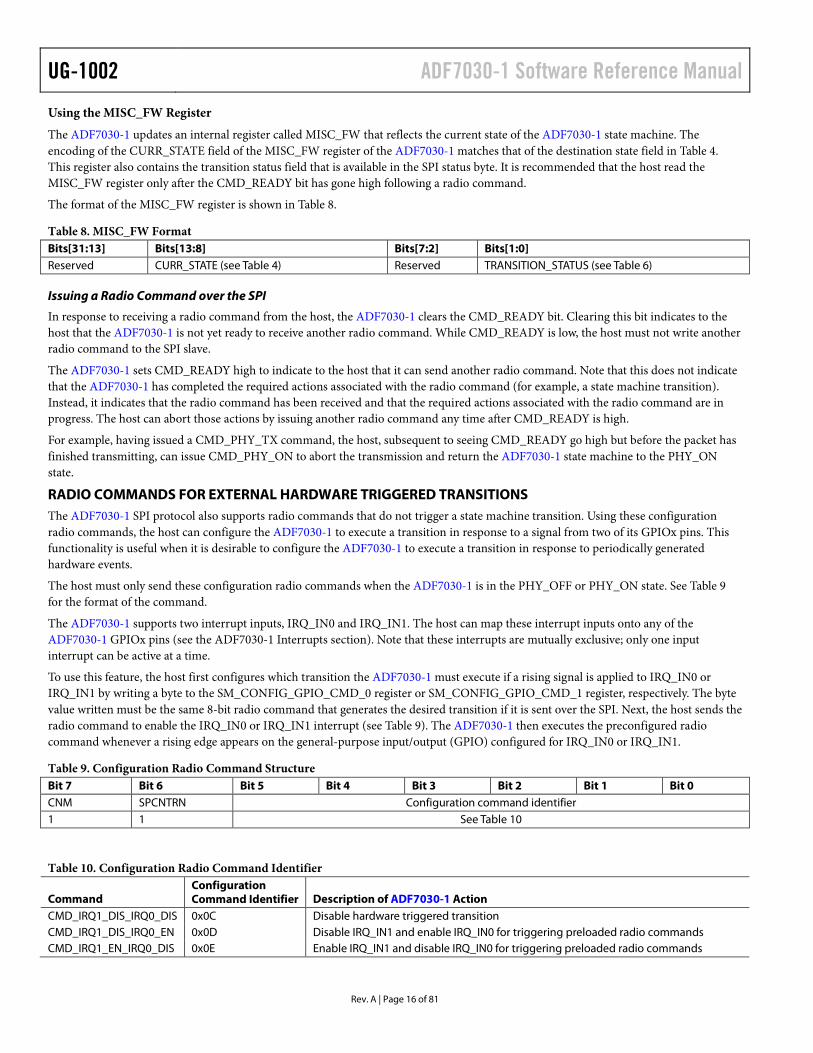
Table 9. Configuration Radio Command Structure Bit 7 Bit 6 Bit 5 Bit 4 Bit 3 Bit 2 Bit 1 Bit 0 CNM SPCNTRN Configuration command identifier 1 1 See Table 10
Table 10. Configuration Radio Command Identifier
Command Configuration Command Identifier Description of ADF7030-1 Action
CMD_IRQ1_DIS_IRQ0_DIS 0x0C Disable hardware triggered transition CMD_IRQ1_DIS_IRQ0_EN 0x0D Disable IRQ_IN1 and enable IRQ_IN0 for triggering preloaded radio commands CMD_IRQ1_EN_IRQ0_DIS 0x0E Enable IRQ_IN1 and disable IRQ_IN0 for triggering preloaded radio commands

ADF7030-1 Software Reference Manual UG-1002
Rev. A | Page 17 of 81
Example of GPIO Triggered Transitions
For the host to trigger a PHY_ON to PHY_TX transition using a low to high transition on a GPIOx pin and a PHY_ON to PHY_OFF state transition using a low to high transition on a separate GPIOx pin, follow these steps:
1. Configure the selected GPIOs as interrupt inputs, IRQ_IN0 and IRQ_IN1 (see the ADF7030-1 Interrupts section). 2. Preload the commands.
a. The host writes the command value for CMD_PHY_TX (0x84) into the 8-bit location at SM_CONFIG_GPIO_CMD_0. b. The host writes the command value for CMD_PHY_OFF (0x81) into the 8-bit location at SM_CONFIG_GPIO_CMD_1.
3. Enable the interrupt inputs. The host enables the ADF7030-1 to execute the preloaded command in response to a rising edge on the IRQ_IN0 or IRQ_IN1 input, respectively, by sending the CMD_IRQ1_EN_IRQ0_EN (0xCF) configuration radio command to the ADF7030-1 over the SPI.
As a result, the ADF7030-1 is configured so that a rising edge on the ADF7030-1 GPIOx pin configured as IRQ_IN0 is equivalent to sending a CMD_PHY_TX command over the SPI to the ADF7030-1.
Similarly, the ADF7030-1 is configured so that a rising edge on a GPIOx pin configured as IRQ_IN1 is equivalent to sending a CMD_PHY_OFF command over the SPI to the ADF7030-1.
The host can track the transition triggered with this method in the same manner as if the radio command was sent over the SPI.
RADIO COMMAND FOR A SYSTEM RESET The host can reset the ADF7030-1 over the SPI using the following sequence:
1. Set Bit 15 and Bit 22 of the CRMGT_PROC_CLK_EN register to 1. Read the register and then write the new value using a 32-bit SPI write (see the Accessing the ADF7030-1 Memory section).
2. Write 0x27 to the SW_KEY bit of the PMU_KEY register using a 32-bit SPI write. 3. Immediately write 0x1 to the HFRC_PD_N bit of the PMU_CLOCKS register using a 32-bit SPI write. 4. Issue the 0xC7 radio reset command to perform a full system reset of the radio.
UG-1002 ADF7030-1 Software Reference Manual
Rev. A | Page 18 of 81
ACCESSING THE ADF7030-1 MEMORY INTRODUCTON The ADF7030-1 SPI supports a flexible memory access protocol that allows the host to access the ADF7030-1 memory efficiently. The protocol supports auto-incrementing addressing for reading or writing blocks of data, base plus offset addressing using three dedicated base address pointers in the ADF7030-1, and individual byte and 4-byte word transfers. See the Host to ADF7030-1 Memory Access Modes section for information about the order of the SPI MISO and MOSI data for each memory protocol. The host is free to choose the protocol that best suits the design of the host SPI.
The host uses the SPI memory access protocols to read and write the memory regions of the ADF7030-1. The format of the SPI transaction starts with a command word with the CNM bit = 0.
The host does not need to monitor the CMD_READY bit before it can read or write ADF7030-1 memory.
All ADF7030-1 RAM can be accessed using byte wide accesses. However, some ADF7030-1 registers must only be accessed using a 32-bit data protocol. This restriction is detailed where relevant.
SUMMARY AND RECOMMENDATIONS There are eight different memory access modes (see Table 11).
Table 11. Access Modes Address Mode Recommended for Accessing Memory Write/Read, Block, No Pointer, Long Address One block of 4-byte words written or read once Memory Write/Read, Block, Pointer Base with Offset Address, Short Address Different subblocks of bytes written or read often within a
larger block of data Memory Write/Read, Block, Pointer, Long Address One block of 4-byte words written or read often Memory Write/Read, Block, Pointer, Short Address One block of bytes written or read often Memory Write/Read, Random, No Pointer, Long Address One 4-byte word written or read once Memory Write/Read, Random, Pointer Base with Offset Supplied, Short Address Different single bytes written or read from within a block Memory Write/Read, Random, Pointer, Long Address One 4-byte word written or read often Memory Write/Read, Random, Pointer, Short Address One byte written or read often
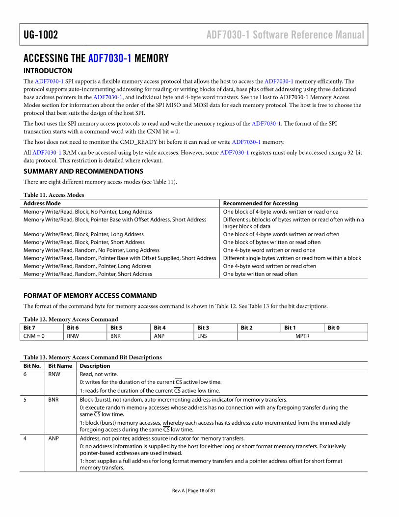
FORMAT OF MEMORY ACCESS COMMAND The format of the command byte for memory accesses command is shown in Table 12. See Table 13 for the bit descriptions.
Table 12. Memory Access Command Bit 7 Bit 6 Bit 5 Bit 4 Bit 3 Bit 2 Bit 1 Bit 0 CNM = 0 RNW BNR ANP LNS MPTR
Table 13. Memory Access Command Bit Descriptions Bit No. Bit Name Description 6 RNW Read, not write. 0: writes for the duration of the current CS active low time.
1: reads for the duration of the current CS active low time.
5 BNR Block (burst), not random, auto-incrementing address indicator for memory transfers. 0: execute random memory accesses whose address has no connection with any foregoing transfer during the
same CS low time.
1: block (burst) memory accesses, whereby each access has its address auto-incremented from the immediately foregoing access during the same CS low time.
4 ANP Address, not pointer, address source indicator for memory transfers. 0: no address information is supplied by the host for either long or short format memory transfers. Exclusively
pointer-based addresses are used instead. 1: host supplies a full address for long format memory transfers and a pointer address offset for short format
memory transfers.

ADF7030-1 Software Reference Manual UG-1002
Rev. A | Page 19 of 81
Bit No. Bit Name Description 3 LNS Long, not short, memory transfer width format. 0: issue a short format, pointer-based, optionally offset, byte wide, byte aligned memory transfer. 1: issue a long format, 32-bit, word aligned, host specified memory transfer. [2:0] MPNTR Base address selection for pointer-based memory accesses. 000: used to set up Pointer 0, Pointer 1, and Pointer 2. 001: reserved. 010: reserved. 011: reserved. 100: reserved. 101: use the contents of Pointer 0 as the base address for pointer-based memory transfers. 110: use the contents of Pointer 1 as the base address for pointer-based memory transfers. 111: use the contents of Pointer 2 as the base address for pointer-based memory transfers.
CONFIGURING THE POINTERS FOR POINTER BASED ACCESSES The host can configure each of the three ADF7030-1 pointers with a 32-bit address for pointer-based addressing. The SPI command used to write to the pointers is 0x28: memory access (CNM = 0), write (RNW = 0), block (BNR = 1), pointer (ANP = 0), long format (LNS = 1), access pointers themselves (MPNTR = 000). See the Memory Write/Read, Block, Pointer, Long Address section for more information.
UG-1002 ADF7030-1 Software Reference Manual
Rev. A | Page 20 of 81
CONFIGURING THE ADF7030-1 The ADF7030-1 transceiver can be configured for different frequency bands, data rates, frequency deviations, and packet formats. From a user perspective, configuring the ADF7030-1 entails writing register settings to the BBRAM section of the radio memory over the SPI. The layout of the radio memory is described in the ADF7030-1 Memory Architecture section. See Figure 2 for an overview of the memory layout.
From a user perspective, the ADF7030-1 has the following three sections in memory used for configuring the radio:
• The radio profile area, profile, stores the radio RF settings. This area includes the channel frequency, CCA settings, low power mode configuration, and GPIO configuration.
• The packet area, GENERIC_PACKET, stores packet configuration settings for both the generic packet format and IEEE802.15.4g packet format. This area includes the packet length, payload location, sync word or PHR length, and value and CRC/FCS configurations.
• Various lookup tables (LUTs) are stored in memory. These LUTs are used for configuring internal radio blocks and running and storing the results from calibrations.
As shown in the ADF7030-1 register map, the contents of the lookup tables and many of the fields in the profile and generic packet sections are labeled as generated. These fields are generated by the ADF7030-1 design center graphical user interface (GUI) based on the RF and packet settings of the user. This ADF7030-1 design center is part of the EZ-KIT® design suite, a set of tools for configuring and evaluating Analog Devices low power integrated transceiver products. It is available for download at www.analog.com. The ADF7030-1 design center contains a Radio Configuration tab that allows a user to enter their desired RF and packet settings. The ADF7030-1 design center generates a corresponding configuration (CFG) file for these settings, containing all required radio settings, including the appropriate LUTs, that can then be written to the device by the user.
The first step in using the ADF7030-1, called the initial configuration, is applying settings generated by the ADF7030-1 design center to the device. After this configuration step, a user can optionally choose to modify some settings while the device is running.
INITIAL CONFIGURATION The following steps are required to set up the ADF7030-1 upon a cold startup:
1. Generate the user settings in the ADF7030-1 design center. Enter the desired RF and packet settings in the Radio Configuration tab of the ADF7030-1 design center. This produces an ADF7030-1 configuration file to write to the radio. This file contains memory radio and packet configuration and the appropriate LUTs. See the ADF7030-1 Configuration File Format section for a detailed explanation of the configuration file format.
2. Write/download the user settings to the ADF7030-1. The contents of the ADF7030-1 configuration file are written to the ADF7030-1 in PHY_OFF over the SPI. See Host Initialization of ADF7030-1 SPI for instructions on issuing a SPI command after a cold start or wakeup from sleep. See the Applying the ADF7030-1 Configuration section for a detailed explanation of how to interpret the configuration file and write it to the radio.
3. Apply the user settings. The host microcontroller sends a CMD_CFG_DEV command. The radio returns to PHY_OFF. See the Configuring section for more information.
MODIFYING CONFIGURATION AT RUN TIME Some radio and packet settings can be modified after the initial configuration step.
The ADF7030-1 settings can be subdivided into two categories, generated settings and run-time settings.
Generated Settings
These settings cannot be calculated by the user. They are generated by the ADF7030-1 design center and must not be overwritten by the user. Change these values only when a new, full configuration file is applied to the device. These private fields can be single or multiple bit fields in a register, marked as generated in the register map, or a full 32-bit register. Examples of a fully generated register include the PROFILE_OCL_CFG0 register.
ADF7030-1 Software Reference Manual UG-1002
Rev. A | Page 21 of 81
Run-Time Settings
Run-time settings can be changed after the initial configuration by the user.
These fields are documented and public. They include fields from the radio profile, such as channel frequency, which can be changed in PHY_ON, for example, between a Rx and Tx transfer. Another example is the PA power and PA selection.
All packet configuration settings can be changed in PHY_OFF and PHY_ON, including, for example, the sync word and the payload length.
The interrupt source and pin output configuration can be reconfigured in PHY_OFF and PHY_ON, for example, by changing the interrupt request (IRQ) mask for IRQ_OUT0 to enable an interrupt on the preamble found interrupt.
GPIO functionality can be altered by the user at run time, for example, by enabling the transmit or receive clock, SPORT_TRXCLK, on a selected pin. A CMD_CFG_DEV command is required for these changes to take effect.
The RTC period can also be changed, requiring a CMD_CFG_DEV command.

UG-1002 ADF7030-1 Software Reference Manual
Rev. A | Page 22 of 81
APPLYING THE ADF7030-1 CONFIGURATION FILE An ADF7030-1 configuration file is a standardized file format for representing memory writes to the ADF7030-1. The ADF7030-1 configuration file format is used to store and apply radio settings, packet settings, lookup tables, and packet payload data generated by the ADF7030-1 design center to the radio. Firmware modules, such as the OfflineCalibration.cfg firmware module, are also supplied as configuration files.
ADF7030-1 CONFIGURATION FILE FORMAT An ADF7030-1 configuration file is an ASCII text file. At the top of the file, a C99 ISO/IEC 9899:1999 standard compliant multilevel comment describes the content of the file and provides a version or time stamp.
There can be one or more blocks in an ADF7030-1 configuration file. A block represents a single SPI transaction and is formatted as a sequence of bytes separated by commas, that is, integers between 0 and 255, written in two-digit wide hexadecimal notation, for example, 0x2E. A block may be preceded by an additional C style comment. Each block starts with a framing header of three bytes, which contains the length of the block, including the length of the frame itself. The length header byte order is most significant byte first. For example, a block length of 300 bytes starts with a sequence of 0x00, 0x01, 0x2C, where 0x00012C is 300 in hexadecimal.
Table 14. ADF7030-1 Configuration File Block Format Length Header SPI Command Sequence Three Bytes, Most Significant Byte First Sequence of Bytes
Table 15. Example of an ADF7030-1 Configuration File Block Format, Showing a Block Write to Address 0x2000060C Length Header SPI Commands Three Bytes Indicating a 16-Byte block Block Write Starting Address 8 Bytes of Data 0x00, 0x00, 0x0F 0x38 0x20, 0x00, 0x06, 0x0C 0xB1, 0xB2, 0xB3, 0xB4, 0xB5, 0xB6, 0xB7, 0xB8
The following is an example of a configuration file, where 0xL0, 0xL1, and 0xL2 are the length bytes in the block header of each block and 0xB1 to 0xBn are the data bytes to be written to the radio memory.
/*
*****************************************************************************
** use_case4.cfg source file generated on June 26, 2016 at 20:04:02
**
** Copyright (C) 2015-2016 Analog Devices Inc., All Rights Reserved.
**
** This file was generated automatically based upon parameters passed to the
** Calculator Library.
**
** For descriptions of each parameter, please refer to Calculator Library Help.
**
** CHANNEL_FREQUENCY 915000000
** DATA_RATE 12500.00
** FREQUENCY_DEVIATION 50000.00
<TRUNCATED>
** TEST_MODES0_TX_TEST 0
**
*/
/* Write to profile memory at 0x20002E4 with word access*/
0xL0, 0xL1, 0xL2, 0x38, 0x20, 0x00, 0x02, 0xE4,
0xB1, 0xB1, 0xB1, 0xB1, 0xB1, 0xB1, 0xB1, 0xB1
...

ADF7030-1 Software Reference Manual UG-1002
Rev. A | Page 23 of 81
0xBn-3, 0xBn-2, 0xBn-1, 0xBn
The contents of the configuration file can be easily stored in a C array to assist in writing host microcontroller code.
const uint8_t Radio_Memory_Configuration[ ] = { #include "Settings_ADF7030-1.cfg" };

UG-1002 ADF7030-1 Software Reference Manual
Rev. A | Page 24 of 81
ADF7030-1 CALIBRATION To ensure that the ADF7030-1 radio performance meets the data sheet specifications, it is necessary to perform a calibration of the ADF7030-1. The Analog Devices supplied firmware module, OffLineCalibrations.cfg, is required for calibration.
Calibration data is maintained in PHY_SLEEP if BBRAM retention is enabled (RETAIN_SRAM and enable bits in the PROFILE_LPM_CFG0 register are set to 1). If the BBRAM is not retained, the host must reload the calibration data to the ADF7030-1 (see Figure 25).
CALIBRATION GUIDELINES The ADF7030-1 calibration is typically a one-time calibration that can be run as part of a factory calibration routine.
Refer to the ADF7030-1 data sheet for further guidelines.
HOW TO RUN THE RADIO CALIBRATION The following steps are required to perform a calibration of the ADF7030-1 (see Figure 23):
1. Apply power to the ADF7030-1 and allow it to transition to PHY_OFF. 2. With the ADF7030-1 in the PHY_OFF state, apply the configuration file generated by the ADF7030-1 design center for the desired
use case, as described in the Applying the ADF7030-1 Configuration File section. 3. While still in the PHY_OFF state, apply the OffLineCalibrations.cfg firmware module. 4. Write the CAL_ENABLE key (0x20002971) to the SM_DATA_CALIBRATION register to enable the calibration. 5. Issue the CMD_CFG_DEV configuration command. 6. When the radio returns to the PHY_OFF state from the configuring state, issue the CMD_PHY_ON command to place the
ADF7030-1 in the PHY_ON state. 7. In the PHY_ON state, issue the CMD_DO_CAL command. The calibration typically takes 630 ms if all calibrations are enabled. 8. On completion of the calibration, the radio autonomously returns to the PHY_ON state and the CAL_SUCCESS bit in the
PROFILE_RADIO_CAL_CFG1 register is set to 1. 9. Write the CAL_DISABLE key (0x20002A21) to SM_DATA_CALIBRATION.
The calibration results registers, as shown in Table 16, can be read back at this point and stored to facilitate a reload of the calibration settings to these same registers following a subsequent cold start, system reset, or wake from PHY_SLEEP without BBRAM retention.
The OffLineCalibrations.cfg firmware module is not retained if the ADF7030-1 is put into the PHY_SLEEP state, even if BBRAM is retained. To prevent the radio from entering an undefined state during a calibration when the calibration firmware module is no longer present in memory, always disable the calibration by writing the CAL_DISABLE key to SM_DATA_CALIBRATION after a calibration has been performed.
The calibration results are stored in the registers listed in Table 16.
Table 16. Calibration Result Registers Address Register 0x200003C8 PROFILE_RADIO_CAL_RESULTS0 0x200003CC PROFILE_RADIO_CAL_RESULTS1 0x200003D0 PROFILE_RADIO_CAL_RESULTS2 0x200003DC PROFILE_RADIO_CAL_RESULTS5 0x200003E0 PROFILE_RADIO_CAL_RESULTS6 0x200003E4 PROFILE_RADIO_CAL_RESULTS7 0x200003E8 PROFILE_RADIO_CAL_RESULTS8 0x20000844 VCO_CAL_RESULTS_DATA0 0x20000848 VCO_CAL_RESULTS_DATA1 0x2000084C VCO_CAL_RESULTS_DATA2 0x20000850 VCO_CAL_RESULTS_DATA3 0x20000854 VCO_CAL_RESULTS_DATA4 0x20000858 VCO_CAL_RESULTS_DATA5 0x2000085C VCO_CAL_RESULTS_DATA6 0x20000860 VCO_CAL_RESULTS_DATA7
ADF7030-1 Software Reference Manual UG-1002
Rev. A | Page 25 of 81
RESTORING SAVED CALIBRATION RESULTS TO THE ADF7030-1 Following a cold start, system reset, or wakeup from PHY_SLEEP without retained BBRAM, the calibration settings in the ADF7030-1 are lost. However, if the host has saved the results of the previous calibration, these results can be reloaded to the ADF7030-1. Saving the results avoids the necessity of having to rerun calibration, notwithstanding the fact that another calibration may be required because of a time lapse or temperature change.
To reload the results of the last calibration executed, the host processor must follow this sequence:
1. Command the ADF7030-1 into the PHY_OFF state if it is not already in that state. 2. Load the configuration settings into the ADF7030-1 (profile, generic packet, LUTs, packet memory). 3. Write the saved calibration results into the calibration results registers shown in Table 16 to the ADF7030-1. 4. Issue a CMD_CFG_DEV command.
The previous calibration settings are restored at this point.
UG-1002 ADF7030-1 Software Reference Manual
Rev. A | Page 26 of 81
TEMPERATURE SENSOR The ADF7030-1 contains a temperature sensor that returns the temperature as a 12-bit signed value in units of 0.0625°C in the TEMP_OUTPUT bits of the PROFILE_MONITOR1 register.
This ADF7030-1 temperature sensor is not factory calibrated.
EXAMPLE CONVERSION To read the temperature, the host must enter the monitoring state. After the TEMP_OUTPUT bits in the PROFILE_MONITOR1 register are written to by the ADF7030-1, the state machine returns to the PHY_ON state.
PROFILE_MONITOR1_TEMP_OUTPUT = 0x1E8
Obtain the twos complement of TEMP_OUTPUT.
If TEMP_OUTPUT > 211, TEMP_OUTPUT = TEMP_OUTPUT − 212
Then multiply by 0.0625 to convert the unit to degrees Celsius.
Temperature (°C) = 488 × 0.0625 = 30.5°C

ADF7030-1 Software Reference Manual UG-1002
Rev. A | Page 27 of 81
TRANSMITTING AND RECEIVING PACKETS OVERVIEW The host programs the ADF7030-1 to transmit and receive variable or fixed length packets. In preparation for transmitting a packet, the host writes payload data into the ADF7030-1 Tx payload buffer and configures programmable fields in the generic packet memory region. The ADF7030-1 transmits a packet in response to a CMD_PHY_TX command.
In preparation for receiving a packet, the host configures programmable fields in the generic packet memory region and issues a CMD_PHY_RX command to the ADF7030-1. The ADF7030-1 then enters the receive state, PHY_RX. If a preamble is detected, the preamble interrupt is set. If the preamble then stops being received, the preamble gone interrupt is set. If subsequently the sync word specified in the packet configuration is detected, the ADF7030-1 proceeds to receive the payload and saves the payload of the packet in the Rx payload buffer.
As a packet is received or transmitted, the ADF7030-1 generates events that can be configured to cause external interrupts on the selected external GPIOx pins.
PACKET MEMORY The ADF7030-1 packet memory is reserved for Rx and Tx payload buffers. The host configures a Tx payload buffer and an Rx payload buffer within the packet memory.
The host can overlap the Rx and Tx payload buffers or can configure two nonoverlapping payload buffers. The start locations of the Rx and Tx payload buffers are set via the PTR_RX_BASE and PTR_TX_BASE bits, respectively, in the GENERIC_PKT_BUFF_CFG0 register. By default, these fields both point to the start of the packet memory. The sizes of the Rx and Tx payload buffers are set via the RX_SIZE and TX_SIZE bits, respectively, in the GENERIC_PKT_BUFF_CFG1 register. By default, these bits are both 256 bytes. The host is responsible for ensuring that the Rx and Tx payload buffers do not extend outside the ADF7030-1 packet memory.
The maximum size of the Tx payload buffer is 511 bytes. The maximum size of the Rx payload buffer is 511 bytes. See the Rolling Buffers Mode section for payloads greater than 511 bytes.
Note that Analog Devices reserves the right to use the packet memory for future functionality upgrades. Contact Analog Devices to use space other than packet memory for the Rx and Tx payload buffers.
PACKET FORMATS The ADF7030-1 supports two packet formats: generic and IEEE802.15.4g. The host selects the packet format used for Rx and Tx via the TYPE_FRAME0 bit in the PROFILE_PACKET_CFG register. The Generic Packet Format section and the IEEE802.15.4g Packet Format section describe the supported packet formats.
UG-1002 ADF7030-1 Software Reference Manual
Rev. A | Page 28 of 81
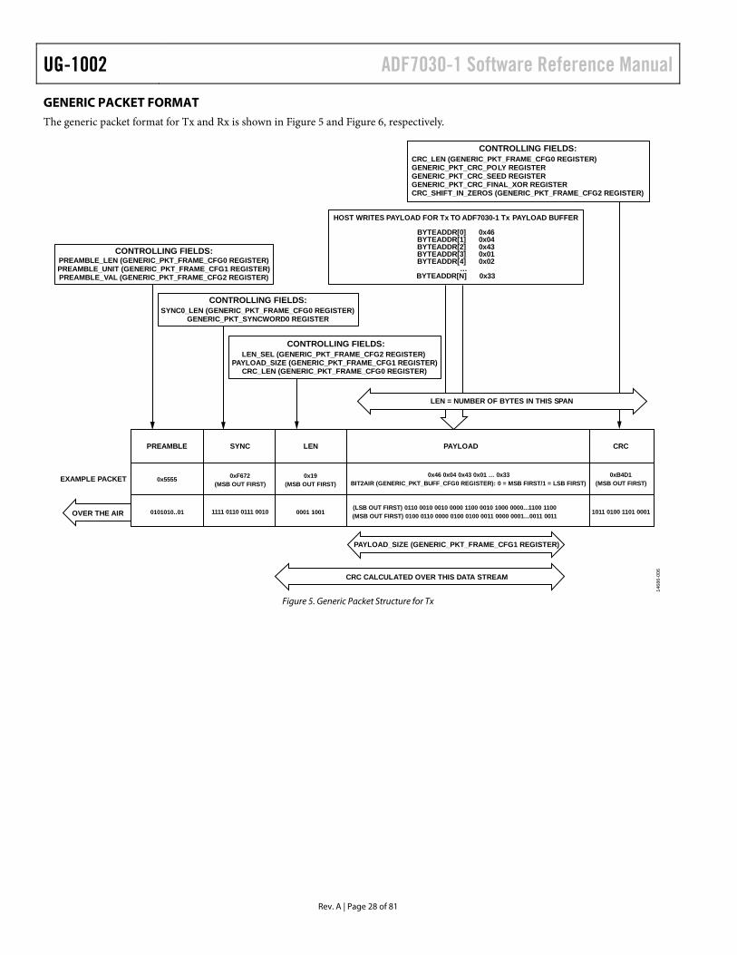
GENERIC PACKET FORMAT The generic packet format for Tx and Rx is shown in Figure 5 and Figure 6, respectively.
0x5555 0xF672(MSB OUT FIRST)
0x19(MSB OUT FIRST)
0x46 0x04 0x43 0x01 … 0x33BIT2AIR (GENERIC_PKT_BUFF_CFG0 REGISTER): 0 = MSB FIRST/1 = LSB FIRST)
0xB4D1(MSB OUT FIRST)
0101010..01 1111 0110 0111 0010 0001 1001(LSB OUT FIRST) 0110 0010 0010 0000 1100 0010 1000 0000...1100 1100(MSB OUT FIRST) 0100 0110 0000 0100 0100 0011 0000 0001...0011 0011
1011 0100 1101 0001
SYNC0_LEN (GENERIC_PKT_FRAME_CFG0 REGISTER)GENERIC_PKT_SYNCWORD0 REGISTER
CONTROLLING FIELDS:
CONTROLLING FIELDS:
CONTROLLING FIELDS:
CONTROLLING FIELDS:
PREAMBLE_LEN (GENERIC_PKT_FRAME_CFG0 REGISTER)PREAMBLE_UNIT (GENERIC_PKT_FRAME_CFG1 REGISTER)PREAMBLE_VAL (GENERIC_PKT_FRAME_CFG2 REGISTER)
LEN_SEL (GENERIC_PKT_FRAME_CFG2 REGISTER)PAYLOAD_SIZE (GENERIC_PKT_FRAME_CFG1 REGISTER)
CRC_LEN (GENERIC_PKT_FRAME_CFG0 REGISTER)
HOST WRITES PAYLOAD FOR Tx TO ADF7030-1 Tx PAYLOAD BUFFER
BYTEADDR[0] 0x46BYTEADDR[1] 0x04BYTEADDR[2] 0x43BYTEADDR[3] 0x01BYTEADDR[4] 0x02
…BYTEADDR[N] 0x33
OVER THE AIR
PREAMBLE SYNC LEN PAYLOAD CRC
EXAMPLE PACKET
PAYLOAD_SIZE (GENERIC_PKT_FRAME_CFG1 REGISTER)
CRC CALCULATED OVER THIS DATA STREAM
CRC_LEN (GENERIC_PKT_FRAME_CFG0 REGISTER)GENERIC_PKT_CRC_POLY REGISTERGENERIC_PKT_CRC_SEED REGISTERGENERIC_PKT_CRC_FINAL_XOR REGISTERCRC_SHIFT_IN_ZEROS (GENERIC_PKT_FRAME_CFG2 REGISTER)
LEN = NUMBER OF BYTES IN THIS SPAN
1468
6-00
6
Figure 5. Generic Packet Structure for Tx

ADF7030-1 Software Reference Manual UG-1002
Rev. A | Page 29 of 81
CONTROLLING FIELDS:
CONTROLLING FIELDS:
CONTROLLING FIELDS:
BYTEADDR[0] 0x46BYTEADDR[1] 0x04BYTEADDR[2] 0x43BYTEADDR[3] 0x01BYTEADDR[4] 0x02
…BYTEADDR[N] 0x33
0x55550xF672
(MSB IN FIRST)0x19
(MSB IN FIRST) 0x46 0x04 0x43 0x01 … 0x330xB4D1
(MSB IN FIRST)
0101010..01 1111 0110 0111 0010 0001 1001 (MSB IN FIRST) 0100 0110 0000 0100 0100 0011 0000 0001...0011 0011 1011 0100 1101 0001
RECEIVED INTO ADF7030-1 Rx PAYLOAD BUFFER
OVER THE AIR
PREAMBLE SYNC LEN PAYLOAD CRC
EXAMPLE PACKET
CRC CALCULATED OVER THIS DATA STREAM
CONTENTS ARE SAVED TORX_LENGTH (GENERIC_PKT_FRAME_CFG3 REGISTER)
SYNC0_LEN (GENERIC_PKT_FRAME_CFG0 REGISTER)GENERIC_PKT_SYNCWORD0 REGISTER
LEN_SEL (GENERIC_PKT_FRAME_CFG2 REGISTER)
CRC_LEN (GENERIC_PKT_FRAME_CFG0 REGISTER)GENERIC_PKT_CRC_POLY REGISTERGENERIC_PKT_CRC_SEED REGISTERGENERIC_PKT_CRC_FINAL_XOR REGISTERCRC_SHIFT_IN_ZEROS (GENERIC_PKT_FRAME_CFG2 REGISTER)
LEN = NUMBER OF BYTES IN THIS SPAN
1468
6-00
7
Figure 6. Generic Packet Structure for Rx
Generic Packet Tx
The following sections describe the bits used by the ADF7030-1 in transmitting a generic packet.
Preamble
The number of preamble bits transmitted is controlled by the PREAMBLE_UNIT bit in the GENERIC_PKT_FRAME_CFG1 register and the PREAMBLE_LEN bits in the GENERIC_PKT_FRAME_CFG0 register.
The preamble pattern transmitted is 0x55 by default. However, the host can program an alternative pattern for preamble transmission via the PREAMBLE_VAL bits in the GENERIC_PKT_FRAME_CFG2 register.
The ADF7030-1 generates the preamble detect event when the first bit of preamble is being transmitted. The ADF7030-1 generates the preamble gone event when the last bit of preamble has been transmitted.
Sync
The host specifies the number of bits of the sync word in a transmitted packet by the SYNC0_LEN bits in the GENERIC_PKT_FRAME_CFG0 register. Note that if this is less than 32, the least significant bits of the GENERIC_PKT_SYNCWORD0 register are used to create the sync word. The sync word is transmitted over the air with the higher bits transmitted first.
The following restrictions apply to the sync word and preamble for a generic packet Tx:
The value of the SYNC0_LEN bits in the GENERIC_PKT_FRAME_CFG0 register must be between 8 and 32, inclusive. SYNC0_LEN + (PREAMBLE_LEN × 2) must be at least 32. The ADF7030-1 generates the sync word detect event when the last bit of sync has been transmitted.

UG-1002 ADF7030-1 Software Reference Manual
Rev. A | Page 30 of 81
Length Field (LEN)
The ADF7030-1 sets LEN to the number of bytes of payload plus the length of the CRC field in bytes (rounded up to nearest byte). The host sets the size of LEN (in bytes) with the LEN_SEL bits in the GENERIC_PKT_FRAME_CFG2 register. The ADF7030-1 does not transmit LEN if the host sets LEN_SEL in the GENERIC_PKT_FRAME_CFG2 register to 0.
The ADF7030-1 generates the LEN pattern event when the last bit of LEN is transmitted. If LEN_SEL in the GENERIC_PKT_FRAME_CFG2 register is zero, the ADF7030-1 does not generate a LEN pattern event.
Payload
The host sets the Tx payload size via the PAYLOAD_SIZE bits in the GENERIC_PKT_FRAME_CFG1 register. The Tx payload buffer must be configured to be at least the size of the payload to be transmitted unless rolling buffers are used (see the Rolling Buffers Mode section). The ADF7030-1 does not transmit bytes outside of the Tx payload buffer. If the host specifies a Tx payload size that extends beyond the Tx payload buffer, the transmitted packet is truncated at the point the Tx payload buffer is exceeded.
The ADF7030-1 does not support the case where PAYLOAD_SIZE in the GENERIC_PKT_FRAME_CFG1 register is 0.
The ADF7030-1 generates the payload event when the last bit of the payload is transmitted. The payload event is not generated if the payload is truncated or the Tx is aborted by the host.
The ADF7030-1 generates a payload block event after every multiple of bytes of payload transmissions set by the TRX_BLOCK_SIZE bits in the GENERIC_PKT_BUFF_CFG1 register. There are no payload block events generated if TRX_BLOCK_SIZE = 0.
CRC
The ADF7030-1 calculates the CRC for the transmitted packet as follows:
1. The ADF7030-1 initializes the CRC of a size set by the CRC_LEN bits in the GENERIC_PKT_FRAME_CFG0 register with the contents of the GENERIC_PKT_CRC_SEED register. The GENERIC_PKT_CRC_POLY register is the polynomial used by the ADF7030-1 CRC calculator.
2. The contents of LEN (if LEN_SEL is nonzero in the GENERIC_PKT_FRAME_CFG2 register) is input into the CRC calculator (most significant byte first) followed by the payload bytes. Note that the payload bytes are input into the CRC calculator most significant bit first, that is, as they are stored in the Tx payload buffer, and not necessarily as they are transmitted over the air.
3. The ADF7030-1 checks the CRC_SHIFT_IN_ZEROS bit in the GENERIC_PKT_FRAME_CFG2 register and, if set, the CRC seed is input into the CRC calculator. Set this field only when the CRC seed (GENERIC_PKT_CRC_SEED) is zero.
4. The result of the CRC calculation is XOR’d with the GENERIC_PKT_CRC_FINAL_XOR register. The result of this XOR is then the CRC value that the ADF7030-1 inserts into the CRC field of the packet being transmitted. After the ADF7030-1 has transmitted the CRC, the ADF7030-1 generates the CRC event.
If CRC_LEN in the GENERIC_PKT_FRAME_CFG0 register is zero, the ADF7030-1 does not generate the CRC event and there is no CRC field in the transmitted packet.
If CRC_LEN in the GENERIC_PKT_FRAME_CFG0 register is not a multiple of eight bits, LEN is rounded up to the nearest byte.
End of Frame (EOF)
The ADF7030-1 generates the EOF event after the complete packet is transmitted or aborted, for example, the host issues a radio command that triggers an exit from the PHY_TX state before packet transmission is complete, and the PA has been ramped down. If the ADF7030-1 controls an external PA with a GPIOx pin, the ADF7030-1 generates the EOF event after the ADF7030-1 disables the external PA.
Order of Bits over the Air in Generic Packet Transmission
The ADF7030-1 transmits the preamble, sync word, length, and CRC with the most significant bit appearing over the air first. However, the host can configure the ADF7030-1 to transmit the payload bytes most or least significant bits first via the BIT2AIR bit in the GENERIC_PKT_BUFF_CFG0 register.
Generic Packet Rx
The following sections describe the fields used by the ADF7030-1 in receiving a generic packet.
Preamble
The ADF7030-1 uses preamble detection as an indicator of an incoming packet. The ADF7030-1 generates the preamble detect event when it detects a preamble. Having detected the preamble, the ADF7030-1 generates the preamble gone” event when the incoming signal no longer contains a preamble.

ADF7030-1 Software Reference Manual UG-1002
Rev. A | Page 31 of 81
Sync
The host writes the sync word to be matched in incoming packets to the GENERIC_PKT_SYNCWORD0 register. The host writes the size of the qualifying sync word (in bits) to the SYNC0_LEN bits in the GENERIC_PKT_FRAME_CFG0 register. If the SYNC0_LEN bits are set to less than 32, the lower significant bits of the GENERIC_PKT_SYNCWORD0 register are used. For example, if GENERIC_PKT_ SYNCWORD0 is 0x12345678 but SYNC0_LEN is 16, the sync word used for packet qualification is 0x5678. The sync word in an incoming packet is decoded as most significant bits received first over the air.
The value of the SYNC0_LEN bits in the GENERIC_PKT_FRAME_CFG0 register must be between 8 and 32, inclusive. The value of the SYNC1_LEN bits in the GENERIC_PKT_FRAME_CFG2 register must be set to 0.
The ADF7030-1 generates the sync detect event when the SYNC0_LEN bits in the GENERIC_PKT_FRAME_CFG0 register following the preamble gone interrupt matches the configured sync.
Length Field (LEN)
The ADF7030-1 supports the reception of packets with variable or fixed length payloads. A variable length payload packet contains a LEN field that indicates the number of bytes from the end of the sync word to the end of the packet (that is, payload plus CRC). A fixed length packet does not contain LEN. Fixed length payloads can be used to receive packets that do not conform to the generic packet structure.
The host configures the ADF7030-1 for fixed length payload operation by setting the LEN_SEL bits in the GENERIC_PKT_FRAME_CFG2 register to 0. For fixed length payload operation, the host configures the ADF7030-1 to read a fixed number of payload bytes from the received packets using the PAYLOAD_SIZE bits in the GENERIC_PKT_FRAME_CFG1 register. Note that this does not include the number of CRC bits that may be appended after the fixed payload.
For variable length payload operation, the host selects between an 8-bit and a 16-bit LEN field by setting the LEN_SEL bits to 1 or 2, respectively, in the GENERIC_PKT_FRAME_CFG2 register.
The ADF7030-1 generates the LEN pattern event when the LEN field is received. If LEN_SEL in the GENERIC_PKT_FRAME_CFG2 register is zero (that is, fixed length packet), the ADF7030-1 does not generate a LEN pattern event.
Payload
The ADF7030-1 writes the received payload into the Rx payload buffer. The Rx payload buffer must be configured to be at least the size of the maximum payload to be received unless rolling buffers are used (see the Rolling Buffers Mode section). The ADF7030-1 does not write received payload bytes outside of the Rx payload buffer. After the Rx payload is filled, remaining payload bytes are lost.
The ADF7030-1 generates the payload event when the last bit of the payload is received. This event is not transmitted if the payload is truncated or if the Rx is aborted by the host before the full payload is received.
The ADF7030-1 generates a payload block event in the payload after every multiple of bytes set by the TRX_BLOCK_SIZE bits in the GENERIC_PACKET_BUFF_CFG1 register. There are no payload block events generated if TRX_BLOCK_SIZE = 0.
CRC
The ADF7030-1 packet reception firmware compares the CRC in the incoming packet against the CRC value calculated over the length and received payload. The ADF7030-1 CRC calculation is as follows:
1. The ADF7030-1 initializes the CRC of size set by the CRC_LEN bits in the GENERIC_PKT_FRAME_CFG0 register with the GENERIC_PKT_CRC_SEED register. The ADF7030-1 uses the GENERIC_PKT_CRC_POLY register as the polynomial in the CRC calculation.
2. As the incoming packet arrives, the contents of LEN (if present) is input into the CRC calculator (most significant byte first), followed by the payload bytes. Note that the payload bytes are input into the CRC calculator with the endianness as they appear in memory, not necessarily in the bit order they are received over the air.
3. The ADF7030-1 checks the CRC_SHIFT_IN_ZEROS bit in the GENERIC_PKT_FRAME_CFG2 register and, if set, the CRC seed is input into the CRC calculator. Set this field only if the CRC seed (GENERIC_PKT_CRC_SEED) is zero.
4. The result of the CRC calculator is XOR’d with the GENERIC_PKT_CRC_FINAL_XOR register. The result of this XOR is then the CRC value that the ADF7030-1 expects to receive in the CRC field of the incoming packet. If the received CRC matches the calculated CRC, the ADF7030-1 generates a CRC event.
If CRC_LEN in the GENERIC_PKT_FRAME_CFG0 register is zero, the ADF7030-1 does not generate a CRC event and all packets are assumed to have been received.
If CRC_LEN in the GENERIC_PKT_FRAME_CFG0 register is not a multiple of eight bits, the received length field value must be the sum of the payload bytes plus CRC_LEN, rounded up to the nearest byte to allow the reception of all the CRC bits.

UG-1002 ADF7030-1 Software Reference Manual
Rev. A | Page 32 of 81
End of Frame
The ADF7030-1 generates the EOF event after the full packet is received or the Rx is aborted by the host issuing a radio command that causes an exit from the PHY_RX state.
Generic Packet Payload Only Tx Mode
The host can configure the ADF7030-1 to transmit a payload only. This mode is known as generic packet payload only Tx and is enabled by setting the TX_BUFF_RAWDATA bit in the GENERIC_PKT_BUFF_CFG1 register. The ADF7030-1 transmits bytes (size set by the PAYLOAD_SIZE bits in the GENERIC_PKT_FRAME_CFG1 register) from the Tx payload buffer. No preamble, sync word, LEN, or CRC is transmitted.
The ADF7030-1 generates the payload event when the last bit of the payload is transmitted. The ADF7030-1 generates the EOF event when the PA has ramped down. If the ADF7030-1 is configured to control an external PA, the ADF7030-1 generates the EOF event coincident with the disable signal to the external PA. No other events are generated.
BYTEADDR[0] 0x46BYTEADDR[1] 0x04BYTEADDR[2] 0x43BYTEADDR[3] 0x01BYTEADDR[4] 0x02
…BYTEADDR[N] 0x33
0x46 0x04 0x43 0x01 … 0x33BIT2AIR (GENERIC_PKT_BUFF_CFG0 REGISTER): 0 = MSB FIRST, 1 = LSB FIRST
(LSB OUT FIRST) 0110 0010 0010 0000 1100 0010 1000 0000... 1100 1100(MSB OUT FIRST) 0100 0110 0000 0100 0100 00 11 0000 0001...0011 0011
HOST WRITES PAYLOAD FOR Tx TO ADF7030-1 Tx PAYLOAD BUFFER
OVER THE AIR
PAYLOAD
EXAMPLE PACKET
PAYLOAD_SIZE (GENERIC_PKT_FRAME_CFG1 REGISTER)
1468
6-00
8
Figure 7. Generic Packet Raw Mode Tx

ADF7030-1 Software Reference Manual UG-1002
Rev. A | Page 33 of 81
IEEE802.15.4g PACKET FORMAT The host configures IEEE802.15.4g packets using many of the same fields as used for generic format packets. The IEEE802.15.4g Tx and Rx packet formats shown in Figure 8 and Figure 9, respectively.
CONTROLLING FIELDS:
CONTROLLING FIELDS: CONTROLLING FIELDS:
CONTROLLING FIELDS:
SHR PSDU
FCS CALCULATED OVER THIS DATA STREAM PRIOR TO FEC, WHITENING
CRC_LEN REGISTER (GENERIC_PKT_FRAME_CFG0 REGISTER)GENERIC_PKT_FRAME_CRC_PO LY REGISTERGENERIC_PKT_FRAME_CRC_SEED REGISTERGENERIC_PKT_FRAME_CRC_FINAL_XOR REGISTERCRC_SHIFT_IN_ZEROS (GENERIC_PKT_FRAME_CFG2 REGISTER)TX_PHR.FCS (GENERIC_PKT_FRAME_CFG5 REGISTER)
PREAMBLE SYNC PAYLOAD FCS
GENERIC_PKT_SYNCWORD0 REGISTERGENERIC_PKT_SYNCWORD1 REGISTERSYNC0_LEN (GENERIC_PKT_FRAME_CFG0 REGISTER)SYNC1_LEN (GENERIC_PKT_FRAME_CFG2 REGISTER)ENDEC_MODE[3] (GENERIC_PKT_FRAME_CFG2 REGISTER)
PREAMBLE_LEN (GENERIC_PKT_FRAME_CFG0 REGISTER)PREAMBLE_UNIT (GENERIC_PKT_FRAME_CFG1 REGISTER)PREAMBLE_VAL (GENERIC_PKT_FRAME_CFG2 REGISTER)
TX_PHR (GENERIC_PKT_FRAME_CFG5 REGISTER)LEN_SEL (GENERIC_PKT_FRAME_CFG2 REGISTER)
PHR
L10 TO L0 IN PHR INDICATES THIS LENGTH IN OCTETS
PHR
1468
6-00
9
Figure 8. IEEE802.15.4g Packet Structure for Tx
SHR PSDU
FCS CALCULATED OVER THIS DATA STREAM POST DE-WHITENING, FEC
PREAMBLE SFD PAYLOAD FCS
SAVED TO RX_LENGTH (GENERIC_PKT_FRAME_CFG3 REGISTER)
PHR
L10 TO L0 IN RECEIVED PHR INDICATES THIS LENGTH IN OCTETS
PHR
GENERIC_PKT_SYNCWORD0 REGISTERGENERIC_PKT_SYNCWORD1 REGISTERSYNC0_LEN (GENERIC_PKT_FRAME_CFG0 REGISTER)SYNC1_LEN (GENERIC_PKT_FRAME_CFG2 REGISTER)
CRC_SHIFT_IN_ZEROS (GENERIC_PKT_FRAME_CFG2 REGISTER)GENERIC_PKT_FRAME_CRC_FINAL_XOR REGISTER
CONTROLLING FIELDS:
CONTROLLING FIELDS:
1468
6-01
0
Figure 9. IEEE802.15.4g Packet Structure for Rx
UG-1002 ADF7030-1 Software Reference Manual
Rev. A | Page 34 of 81
IEEE802.15.4g Packet Transmission
The following sections describe the fields used by the ADF7030-1 in transmitting an IEEE802.15.4g packet.
Preamble
The number of preamble 01010101 octets in the outgoing packet is specified by the PREAMBLE_LEN bits in the GENERIC_PKT_FRAME_ CFG0 register. The host must set PREAMBLE_UNIT in the GENERIC_PKT_FRAME_CFG1 register to 1 to indicate that PREAMBLE_LEN in the GENERIC_PKT_FRAME_CFG0 register indicates octets of preamble, not bits. The host must also set the PREAMBLE_VAL bits in the GENERIC_PKT_FRAME_CFG2 register to 0x00 to set the preamble pattern in the transmitted packet to 0x55.
The ADF7030-1 generates the preamble detect event when the first bit of the preamble is being transmitted. The ADF7030-1 generates the preamble gone event when the last bit of preamble is transmitted.
Start Frame Delimiter (SFD)
The host sets Bit 3 of the ENDEC_MODE bits in the GENERIC_PKT_FRAME_CFG2 register to enable FEC encoding. If FEC encoding is enabled, the ADF7030-1 transmits GENERIC_PKT_SYNCWORD0 as the SFD. Otherwise, the ADF7030-1 transmits GENERIC_PKT_ SYNCWORD1 as the SFD. The host must set SYNC0_LEN in the GENERIC_PKT_FRAME_CFG0 register and SYNC1_LEN in the GENERIC_PKT_FRAME_CFG2 register to 16. The SFD is transmitted most significant bit first.
The ADF7030-1 generates the sync detect event when the last bit of SFD is transmitted.
PHY Header (PHR)
The host writes the PHR to be transmitted to the TX_PHR bits in the GENERIC_PKT_FRAME_CFG5 register. The PHR format is as per Section 18.1 of the IEEE802.15.4g-2012 standard (Part 15.4). The host must set LEN_SEL in the GENERIC_PKT_FRAME_CFG2 register to 2.
The ADF7030-1 generates the LEN pattern event when the last bit of the PHR field is transmitted.
PHY Service Data Unit (PSDU)—Payload and Frame Check Sequence (FCS)
The PSDU comprises a payload and an FCS. The host writes the payload part of the PSDU into the Tx payload buffer and the ADF7030-1 calculates the FCS.
The host specifies the PSDU size in octets via the L10 to L0 bits (defined in the IEEE802.15.4g standard) of the TX_PHR bits in the GENERIC_PKT_FRAME_CFG5 register. The ADF7030-1 whitens the PSDU based on the data whitening (DW) bit (defined in the IEEE802.15.4g standard) in the TX_PHR bits.
The ADF7030-1 truncates the payload part of the PSDU if the size of the payload exceeds the size of the Tx payload buffer.
The host configures the FCS type field in the TX_PHR bits (defined in the IEEE802.15.4g standard) to select the FCS size.
Table 17 shows the CRC related bits the host must set for FCS calculation.
Table 17. CRC Bits Used in IEEE802.15.4g Tx FCS Calculation Register Bits FCS161 (FCS Type Field = 1) FCS321 (FCS Type Field = 0) GENERIC_PKT_FRAME_CFG0 CRC_LEN 16 32 GENERIC_PKT_CRC_POLY VAL 0x1021 0x04C11DB7 GENERIC_PKT_FRAME_CFG2 CRC_SHIFT_IN_ZEROS 1 1 GENERIC_PKT_CRC_SEED VAL 0 0x46AF6449 GENERIC_PKT_CRC_FINAL_XOR VAL 0xFFFFFFFF 0xFFFFFFFF 1 FCS16 and FCS32 are defined in the IEEE802.15.4g standard.
The ADF7030-1 calculates the FCS over the payload bytes of the PSDU, adding padding bytes of zero to ensure a multiple of four bytes are used in the FCS calculation. The padding bytes are not transmitted.
The ADF7030-1 FEC encodes the PHR and PSDU if Bit 3 of ENDEC_MODE in the GENERIC_PKT_FRAME_CFG2 register is set.
The ADF7030-1 generates the payload and CRC events when the last bit of the PSDU is transmitted. The payload event is not generated if the payload is truncated or Tx is aborted by the host.

ADF7030-1 Software Reference Manual UG-1002
Rev. A | Page 35 of 81
End of Frame
The ADF7030-1 generates the EOF event after the PA has ramped down following a complete packet transmission or the termination of the transmission caused by the host issuing a radio command that triggers an exit from the PHY_TX state. If the ADF7030-1 is configured to control an external PA, the ADF7030-1 generates the EOF event coincident with the disable signal to the external PA.
IEEE802.15.4g Packet Reception
The following sections describe the fields used by the ADF7030-1 in receiving an IEEE802.15.4g packet.
Preamble
The ADF7030-1 uses preamble detection as an indicator of an incoming packet. The ADF7030-1 generates the preamble detect event when it detects a preamble on the antenna. The ADF7030-1 generates the preamble gone event when the incoming data stream no longer matches the preamble.
SFD
The ADF7030-1 can detect both FEC and nonFEC encoded IEEE802.15.4g packets. However, to do this, it relies on the host having configured the GENERIC_PKT_SYNCWORD0 and GENERIC_PKT_SYNCWORD1 registers with the SFDs corresponding to the FEC encoded and nonFEC encoded packets, respectively, that the ADF7030-1 is to receive.
The host must program the SYNC0_LEN bits in the GENERIC_PKT_FRAME_CFG0 register and the SYNC1_LEN bit in the GENERIC_PKT_FRAME_CFG2 register to be 16. Only 16-bit SFDs are supported.
To configure the ADF7030-1 to receive only FEC encoded packets (that is, ignore nonFEC encoded packets), the host can set SYNC1_LEN in the GENERIC_PKT_FRAME_CFG2 register to 0. However, SYNC0_LEN in the GENERIC_PKT_FRAME_CFG1 register must always be 16.
If FEC is disabled, only the preamble and sync word are FEC encoded.
PHR
The ADF7030-1 writes the received PHR to the RX_LENGTH bits in the GENERIC_PKT_FRAME_CFG3 register, decoding it via FEC if necessary. The ADF7030-1 uses the DW, FCS, and L10 to L0 bits, which are defined in the IEEE802.15.4g standard, in the received PHR to control the handling of the payload and FCS parts of the received PSDU.
PSDU—Payload and FCS
The ADF7030-1 dewhitens the received PSDU based on the DW bit in the received PHR. Based on the SFD match, the ADF7030-1 decodes the received PSDU via FEC. The ADF7030-1 writes the payload part of the dewhitened, FEC decoded PSDU into the Rx payload buffer. The ADF7030-1 pads the received payload to a multiple of four bytes for the FCS calculation but does not write these padding bytes to the Rx payload buffer. The ADF7030-1 does not write the received payload bytes outside of the Rx payload buffer. After the Rx payload is filled, the remaining payload bytes are lost.
Table 18 shows the CRC related bits the host must set for FCS calculation.
Table 18. CRC Bits Used in IEEE802.15.4g Rx FCS Calculation Register Bits FCS16 and FCS321 GENERIC_PKT_FRAME_CFG2 CRC_SHIFT_IN_ZEROS 1 GENERIC_PKT_CRC_FINAL_XOR VAL 0xFFFFFFFF 1 FCS16 and FCS32 are defined in the IEEE802.15.4g standard.
The ADF7030-1 generates the payload event when the complete PSDU is received. If the received FCS matches that calculated over the received PSDU, the ADF7030-1 also generates the CRC event.
End of Frame
The ADF7030-1 generates the EOF event after the full packet is received or the Rx is aborted by the host issuing a radio command that causes an exit from the PHY_RX state.

UG-1002 ADF7030-1 Software Reference Manual
Rev. A | Page 36 of 81
AUTOMATIC FREQUENCY CONTROL (AFC) REPORTING The ADF7030-1 updates a frequency error value that the host can read. The frequency error value is valid during packet reception after the sync word/SFD detect event is generated by the ADF7030-1, but must be read before the end of the packet is received. The frequency error is a signed 16-bit value at the readback bits in the AFC_FREQUENCY_ERROR register. A host must implement the following formula to derive the frequency error in Hz:
Frequency Error (in Hz) = (Readback) × 26,000,000/(222)
This approach is valid for both generic packet and IEEE802.15.4g packet formats.
ROLLING BUFFERS MODE The ADF7030-1 supports long payload handling by proving first in, first out (FIFO) related events for the Rx and Tx payload buffers. The host enables this mode by setting the ROLLING_BUFF_EN bit in the GENERIC_PKT_BUFF_CFG0 register and by configuring the ADF7030-1 to generate interrupts that indicate the payload buffer availability status during packet reception and transmission. See the Clearing Interrupts section for details on enabling the FIFO events to trigger interrupts.
Two FIFO events are shared between Rx and Tx: lower half and upper half. Table 19 shows the meaning of the events for Rx and Tx.
Table 19. Rolling Buffer FIFO Events FIFO Event Meaning for Rx Meaning for Tx Lower Half Lower half of Rx payload buffer has been filled with received payload
bytes Lower half of Tx payload buffer has been transmitted
Upper Half Upper half of Rx payload buffer full with received payload bytes Upper half of Tx payload buffer has been transmitted
Packet Tx with Rolling Buffers
With rolling buffers mode enabled, the host must write the Tx payload to the Tx payload buffer before issuing the CMD_PHY_TX command. The ADF7030-1 generates the lower half event when the ADF7030-1 has transmitted the lower half of the Tx payload buffer.
The host must then refill the lower half of the Tx payload buffer with subsequent payload data for transmission and clear the interrupt triggered by the Lower Half event. See the Clearing Interrupts section for details on clearing interrupts. The ADF7030-1 generates the upper half event when the ADF7030-1 has transmitted the upper half of the Tx payload buffer. This process continues until the full payload has been transmitted. The start of the upper half of the Tx payload buffer is at the following location:
PTR_TX_BASE + floor((TX_SIZE)/2)
where: PTR_TX_BASE is in the GENERIC_PKT_BUFF_CFG0 register. TX_SIZE is in the GENERIC_PKT_BUFF_CFG1 register.
Packet Rx with Rolling Buffers
With rolling buffers mode enabled, the ADF7030-1 generates the lower half event when the lower half of the Rx payload buffer has been filled with received payload data. The host must then read the payload bytes from the lower half of the Rx payload buffer and clear the lower half event. See the Clearing Interrupts section for details on clearing interrupts. The ADF7030-1 generates the upper half event when the upper half of the Rx payload buffer has been filled with the received payload data. The host must then read the payload bytes from the upper half of the Rx payload buffer and clear the upper half event. This process continues until the full payload has been received. Note that the start of the upper half of the Rx payload buffer is at the following location:
PTR_RX_BASE + floor((RX_SIZE)/2)
where: PTR_RX_BASE is in the GENERIC_PKT_BUFF_CFG0 register. RX_SIZE is in the GENERIC_PKT_BUFF_CFG1 register.
Recommended Rolling Buffers Configuration
It is recommended that the Rx payload buffer size be set to one less than the packet memory size the host allocates for the Rx payload buffer.
ADF7030-1 Software Reference Manual UG-1002
Rev. A | Page 37 of 81
When an incoming generic packet payload is one byte longer than a multiple of half the Rx payload buffer size and the rolling buffers are enabled, it is expected that the last payload byte be written to the first byte location within the Rx payload buffer. However, it is instead written to the first location after the end of the Rx payload buffer and the expected upper half event is not generated.
When the last payload byte is written to the first byte location within the upper half of the Rx payload buffer, the final lower half event is not generated but the data is written to the correct location.
In both of these cases, it is recommended that a host use the ADF7030-1 payload event to be informed of the end of the received packet payload.
If the enable bit in the PROFILE_LPM_CFG0 register is set prior to the issuance of PHY_SLEEP and the BBRAM CRC is valid, the rolling buffer configuration is restored on wakeup.
AUTOTURNAROUND The ADF7030-1 supports autoturnaround, a feature whereby the ADF7030-1 autotransitions from PHY_RX to PHY_TX, or vice versa, following the completion of packet reception or packet transmission, respectively.
Rx to Tx Autoturnaround
Following the reception of an incoming packet (generic packet or IEEE802.15.4g), the ADF7030-1 automatically transitions from PHY_RX to PHY_TX and transmits a packet if TURNAROUND_RX in the GENERIC_PKT_BUFF_CFG1 register is set. A complete reception requires a CRC/FCS match or the CRC length (for generic packet only) to be zero. If a packet with a valid CRC is not received, the ADF7030-1 returns to PHY_ON independently of the autoturnaround field.
Tx to Rx Autoturnaround
Following the transmission of a packet (generic packet or IEEE802.15.4g), the ADF7030-1 automatically transitions from PHY_TX to PHY_RX and transmits a packet if TURNAROUND_RX in the GENERIC_PKT_BUFF_CFG1 register is set. A complete reception requires a CRC/FCS match or the CRC length (for generic packet only) to be zero. If a packet is not received, the ADF7030-1 returns to PHY_ON independently of the autoturnaround field.
MODULATION MODES AND LINE ENCODING Generic Packet Format
RX—Modulation
Modulation Type 2FSK/2GFSK is supported for generic packet format Rx.
RX—Line Encoding
Line encoding nonreturn to zero (NRZ) is supported for generic packet format Rx.
TX—Modulation
The 2FSK, 4FSK, and on/off keying (OOK) modulation types are supported for generic packet Tx. However, for 4FSK/4GFSK, a maximum sync word of 32 bits (that is, 16 4FSK/4GFSK symbols) is supported. The value in GENERIC_PKT_SYNCWORD0 is used as the sync word for 4FSK/4GFSK.
TX—Line Encoding
NRZ line encoding is supported for generic packet Tx. The host must set Bit 0 of ENDEC_MODE in the GENERIC_PKT_FRAME_CFG2 register to enable NRZ line encoding for the generic packet format.
Manchester line encoding is supported with OOK modulation for generic packet Tx. For a Manchester encoded packet, the preamble and sync word are not line encoded. The host must set Bit 2 of ENDEC_MODE in the GENERIC_PKT_FRAME_CFG2 register to enable Manchester line encoding.
OOK Bit Framing
If OOK modulation is selected, the invert polarity bit in ENDEC_MODE in the GENERIC_PKT_FRAME_CFG2 register must be set to 0.
OOK Framing
When the ADF7030-1 transmits a bit stream using OOK modulation an external PA can be modulated at the bit level. The host sets the EXT_PA_FRAMING_EN and EXT_PA_OOK_BIT_FRAMING_EN bits in the PROFILE_RADIO_DIG_TX_CFG1 register to enable this mode. See Figure 10 for the OOK bit framing timing diagram and Table 20 for the timing parameters.

UG-1002 ADF7030-1 Software Reference Manual
Rev. A | Page 38 of 81
t4
t2
t1_LOW
t1_HIGH
t3 t3t2
t5 t5
DATA
8 × DATA RATE
ADF7030-1 PA
EXTERNALPA SIGNAL
t4 1468
6-01
1
Figure 10. OOK External PA Bit Framing
Table 20. OOK Bit Framing Times Parameter Value t1_LOW, t1_HIGH 1/data rate t2 Internal ADF7030-1 PA ramp-up time t3 Internal ADF7030-1 ramp-down time t4 (1/(8 × Data Rate)) – 1 µs t5 1 µs
The internal ADF7030-1 PA ramp-up and ramp-down times are identical and are calculated as follows:
Ramp Time/Symbols = PA_FINE/(PA_FINE_INC × 32) + 1/8
where: PA_FINE_INC is derived from PA_RAMP_RATE in the PROFILE_RADIO_DIG_TX_CFG1 register (see Table 21). PA_FINE is in the PROFILE_RADIO_DIG_TX_CFG0 register.
Table 21. Internal ADF7030-1 PA Ramp Times PA_RAMP_RATE in PROFILE_RADIO_DIG_TX_CFG1 Register Minimum PA_FINE_INC 0 Not applicable; ramp time/symbols = 1/16 1 65 2 33 3 17 4 9 5 5 6 3 7 2
IEEE802.15.4g
2FSK/2GFSK modulation and NRZ encoding are supported for IEEE802.15.4g packet format Rx and Tx. The host must set Bit 0 of ENDEC_MODE in the GENERIC_PKT_FRAME_CFG2 register to 1 to enable NRZ line encoding.

ADF7030-1 Software Reference Manual UG-1002
Rev. A | Page 39 of 81
EXTERNAL PA AND LNA CONTROL External LNA
The ADF7030-1 supports the generation of a framing signal to an external LNA via the EXT_LNA_FRAMING_EN bit in the PROFILE_RADIO_DIG_TX_CFG1 register. The ADF7030-1 GPIOx pin used for the external LNA framing signal is set by the EXT_LNA_PIN_SEL bits in the PROFILE_RADIO_DIG_TX_CFG1 register. The ADF7030-1 enables the internal and external LNAs at the same time.
External PA
The ADF7030-1 supports the generation of a framing signal to an external PA via the EXT_PA_FRAMING_EN bit in the PROFILE_RADIO_DIG_TX_CFG1 register. The ADF7030-1 GPIOx pin used for the external PA framing signal is set by the EXT_PA_PIN_SEL bits in the PROFILE_RADIO_DIG_TX_CFG1 register. The external PA is turned off after the ADF7030-1 internal PA has ramped down.
In addition to setting the pin selection field for the PA and LNA in the PROFILE_RADIO_DIG_TX_CFG1 register, the corresponding GPIOx pin configuration in the PROFILE_GPCON0_3 or the PROFILE_GPCON4_7 register must be set to an output. For example, if GPIO3 is selected for the PA output, 0x03 must be written to the EXT_PA_PIN_SEL bits in the PROFILE_RADIO_DIG_TX_CFG1 register and 0x1B must be written to the PIN3_CFG bits in the PROFILE_GPCON0_3 register to set it as an output.
Combined Match
When the ADF7030-1 is used in a combined match (that is, the Rx input and a Tx output are connected passively), the host must set COMBINED_TRX_MATCH in the PROFILE_RADIO_MODES register to 1. Failure to set this field may result in damage to the ADF7030-1 when a CMD_PHY_TX command is issued. If the radio uses a separate match network, set COMBINED_TRX_MATCH to 0.
TEST MODES Transmission (Tx) Test Modes
The ADF7030-1 supports the continuous Tx test modes, which are enabled by setting the TX_TEST bits in the GENERIC_PKT_TEST_ MODES0 register to a nonzero value. The ADF7030-1 continually transmits in the selected mode when in the PHY_TX state. The host must send a PHY_ON command to exit the PHY_TX state.
Tx test modes are only available when generic packet format is selected.
Table 22. Supported Tx Test Modes TX_TEST Test Mode 1 Transmit a carrier. 2 Transmit frequency deviation tone, fDEV, in 2FSK or off in OOK. 3 Transmit fDEV_MAX in 4FSK only. 4 Transmit +fDEV in 2FSK or on in OOK. 5 Transmit +fDEV_MAX in 4FSK only. 6 Transmit preamble pattern. 7 Transmit pseudorandom (PN9) sequence. 8 Transmit a custom pseudorandom sequence.
In addition to PN9, a custom pseudorandom transmit mode is supported. The pattern is configured using the CRC fields outlined in Table 23.
Table 23. Custom Tx Pseudorandom Sequence Configuration Configuration Option Register or Bit Field PN Polynomial GENERIC_PKT_CRC_POLY PN Size (Bytes) CRC_LEN in GENERIC_PKT_FRAME_CFG0 PN Initial Data GENERIC_PKT_CRC_SEED
UG-1002 ADF7030-1 Software Reference Manual
Rev. A | Page 40 of 81
Receive Test Modes
The ADF7030-1 supports a bit error rate (BER) test mode in receive mode, in which the Rx clock and data are made available on the GPIOx pins.
To enable this mode, the radio must be configured in the PHY_OFF state before issuing the CMD_CCA command. Choose a pin to output the receive data and set the appropriate pin configuration value in PROFILE_GPCON0_3 or PROFILE_GPCON4_7 to SPORT_RXDATA. Choose a different GPIOx pin and set its configuration value to SPORT_TRXCLK, for example, setting PIN7_CFG in PROFILE_GPCON4_7 to SPORT_TRXCLK outputs the clock on GPIO7. To disable AFC in CCA mode, set the mode bits in the AFC_CONFIG register to 0. Set DETECTION_TIME in the PROFILE_CCA_CFG register to 0 before issuing the CMD_CCA command. The ADF7030-1 remains in the CCA state indefinitely with the clock and data available on the configured pins.
Configurable Clock Output on GPIOx Pin
The ADF7030-1 supports generating a programmable clock that is synchronous with the ADF7030-1 system clock and outputting the clock on a selected GPIOx pin. This state is nonreturnable. A system reset must be used to exit from this test mode.
To select the GPIOx pin on which the clock is to be generated by the ADF7030-1 in the GPCLK_OUT state, the host must set the appropriate pin configuration. The selected pin configuration in PROFILE_GPCON0_3 or PROFILE_GPCON4_7 must be set to GPCLK_OUT (0x24).
The clock frequency of the generated clock signal is selected by GPIO_CLK_FREQ_SEL in the PROFILE_RADIO_MODES register. These profile fields must be written by the host in the PHY_OFF state before issuing a CMD_CFG_DEV command.
The CMD_GPCLK command, shown in Table 5, must be issued only from the PHY_ON state.

ADF7030-1 Software Reference Manual UG-1002
Rev. A | Page 41 of 81
RSSI, CCA, AND AUTOTURNAROUND RSSI DURING PACKET RECEPTION During packet reception for both generic packet and IEEE802.15.4g formats, the ADF7030-1 makes an RSSI measurement at the instant the sync word is detected and periodically during payload reception, every two bytes of the payload. The ADF7030-1 writes this RSSI value into the RSSI bits in the GENERIC_PKT_LIVE_LINK_QUAL register. RSSI is a signed 11-bit value, which represents the measured power in units of 0.25 dBm, for example, GENERIC_PKT_LIVE_LINK_QUAL = 0x0696 and RSSI = −70 dBm.
CLEAR CHANNEL ASSESSMENT (CCA) The ADF7030-1 state machine CCA state supports clear channel assessment functionality. When in the CCA state, the ADF7030-1 periodically measures the RSSI value in the configured Rx channel and writes this value into the value bits in the PROFILE_CCA_READBACK register. These bits contain the RSSI measurement as a signed 11-bit value in units of 0.25 dBm. The host sets the duration that the ADF7030-1 measures the RSSI using the DETECTION_TIME field in the PROFILE_CCA_CFG register. During the detection period, the ADF7030-1 also updates the LIVE_STATUS bit in the PROFILE_CCA_READBACK register to indicate whether the measured RSSI is above the threshold configured in the threshold bits. This threshold is also a signed 11-bit value in units of 0.25 dBm.
After the detection time has expired, the ADF7030-1 state machine transitions back to the PHY_ON state if the measured RSSI exceeded the programmed threshold at any time during the detection period. Otherwise, when the detection time expires, the ADF7030-1 state machine returns to the PHY_ON state.
If the host sets DETECTION_TIME in the PROFILE_CCA_CFG register to 0 before issuing the CMD_CCA command, the ADF7030-1 remains in the CCA state indefinitely, periodically updating both the value and the LIVE_STATUS bits in the PROFILE_CCA_READBACK register.
In the CCA state, the RSSI is measured every tick for DETECTION_TIME ticks, at the end of which the state machine transitions to either PHY_ON or PHY_TX
CCA DETECTION TIME A duration of a CCA tick is calculated as follows:
(tB) × (TICK_POSTSCALAR + 1)/(CCA Rate Divisor)
where: tB is the data bit time in seconds. TICK_POSTSCALAR is the value as defined in the PROFILE_CCA_CFG register. CCA Rate Divisor is decoded using the Table 24.
Table 24. CCA Detection Time Parameters TICK_RATE (PROFILE_CCA_CFG Register) CCA Rate Divisor 1 1 2 2 3 4 4 8 5 16 6 32 7 64 8 128

UG-1002 ADF7030-1 Software Reference Manual
Rev. A | Page 42 of 81
RSSI OFFSET CALIBRATION The RSSI offset calibration allows the user to accurately calibrate the RSSI readback available from the ADF7030-1. This calibration must be performed for every unique configuration applied to the ADF7030-1.
1. Power on the ADF7030-1. 2. Apply the configuration file generated from the ADF7030-1 design center. The ADF7030-1 design center indicates which receiver
path to use for the generated use case: narrow band or wideband, which can also be read back from the TRX_PHY_MODE bit in the PROFILE_RADIO_MODES register.
3. Perform a calibration as outlined in the ADF7030-1 Calibration section. 4. Clear the existing offset by writing 0 to NB_OFFSET or WB_OFFSET in the PROFILE_RSSI_CFG register, as appropriate. 5. Transition to PHY_ON. 6. Apply a carrier to the radio Rx input at −77 dBm at the channel frequency of the use case. It is recommended to place the carrier in
the middle of RF band in which the radio is operating. 7. Write 0 to DETECTION_TIME in the PROFILE_CCA_CFG register to force the radio to remain in CCA mode when entered for
measurement purposes. 8. Issue the CMD_CCA command. 9. Wait a minimum of 64 times the bit transition time for the programmed use case. 10. Read back 20 RSSI samples. 11. Convert the RSSI samples to dBm and average them. 12. Calculate the error: Error (dBm) = Average (dBm) − Power Input (dBm). 13. Convert the error value to the appropriate offset.
a. For narrow-band use cases, the RSSI offset is measured in 0.25 dBm per code. Write the calculated offset to NB_OFFSET in the PROFILE_RSSI_CFG register.
b. For wideband use cases, the RSSI offset is measured in 0.36 dBm per code. Write the calculated value to WB_OFFSET in the PROFILE_RSSI_CFG register.
14. Issue PHY_ON to exit CCA mode. 15. Revert the DETECTION_TIME setting in the PROFILE_CCA_CFG register as required. 16. Store the offset value for use at run time. This value can be applied when restoring other calibration results.
ADF7030-1 Software Reference Manual UG-1002
Rev. A | Page 43 of 81
LOW POWER MODES PHY_SLEEP The ADF7030-1 consumes low current in the PHY_SLEEP state. The host can configure the ADF7030-1 to retain its BBRAM during PHY_SLEEP. This configuration allows the host to configure the ADF7030-1 memory regions in BBRAM only once. In this state, the ADF7030-1 retains the GPIO configuration and values. The host can also configure the ADF7030-1 to autonomously transition from PHY_SLEEP to PHY_ON when a configurable period of time expires.
The host can also trigger the ADF7030-1 to transition from PHY_SLEEP to PHY_ON by applying a high to low transition on the SPI CS pin. This transition is equivalent to the first step in the SPI initialization sequence (see the Host Initialization of ADF7030-1 SPI section).
The host can also wake up the ADF7030-1 from PHY_SLEEP by applying a rising edge on the GPIO2 or GPIO4 pin (see the GPIO section).
BBRAM Retention
The host configures the ADF7030-1 to retain its BBRAM during PHY_SLEEP by setting the RETAIN_SRAM and enable bits in the PROFILE_LPM_CFG0 register. Changes to these bits are effective only when the host issues a CMD_CFG_DEV command.
Real-Time Clock (RTC)
The ADF7030-1 has its own RTC to provide the periodic wakeup that triggers the transition from PHY_SLEEP to PHY_OFF. The RTC can be clocked from one of two sources: the ADF7030-1 internal 26 kHz (nominal) low frequency RC oscillator (LFRC) or an external 32 kHz clock. See the ADF7030-1 Hardware Reference Manual to connect an external 32 kHz clock source.
The host configures the RTC via the PROFILE_LPM_CFG0 and PROFILE_LPM_CFG1 registers. RTC configuration changes take effect when the ADF7030-1 enters the configuring state.
Enabling the RTC
The RTC must be enabled before it can be used. The RTC_LF_SRC_SEL bit must be set prior to enabling the RTC and the RTC_PERIOD bits in the PROFILE_LPM_CFG1 register must be set to a non-zero value. To enable the RTC, set the RTC_EN bit to 1 and the enable bit to 1 in the PROFILE_LPM_ CFG0 register. These bits must be set in the PHY_OFF state, prior to issuing CMD_CFG_DEV.
When the RTC is configured for the first time since the last cold start or system reset, it must perform a power-up sequence. This procedure takes approximately 200 ms when the RTC clock source is the internal LFRC clock, or 3600 ms when the RTC clock source is an external 32 kHz clock source (see the ADF7030-1 data sheet for more information).
The RTC can use either the internal 26 kHz low frequency RC (LFRC) oscillator or a 32 kHz external low frequency crystal (LFXTAL) as a clock source. The source selection is controlled by RTC_LF_SRC_SEL, where 0 selects the LFRC and 1 selects the LFXTAL.
The LFRC must be calibrated to ensure timing accuracy. This calibration is not performed automatically and must be invoked using the CMD_LFRC_CAL command from the PHY_ON state. The LFRC calibration requires that the OfflineCalibration.cfg firmware module be applied to the radio and the CAL_ENABLE key be written to the SM_DATA_CALIBRATION register. See the ADF7030-1 Calibration section for more information. RTC must be enabled and configured for the calibration to succeed. This calibration does not need to be completed again if the RTC is enabled when the ADF7030-1 enters PHY_SLEEP.
Reconfiguration
RTC is configured only upon entry to the configuring state when the RTC_RECONFIG_EN bit is set in the PROFILE_LPM_CFG0 register. This flag is automatically cleared each time a new RTC configuration is applied. The flag defaults to 1 following a cold start, system reset, or wakeup from PHY_SLEEP if the BBRAM is not retained.
Periodic Wakeup
The ADF7030-1 can be configured to wake up on a periodic interval using the RTC, the default configuration that takes effect simply by enabling the RTC.
The duration of a period is measured in ticks of the RTC clock (nominally 32.768 kHz) and may range from 450 µs to 36 hours at that frequency. This value is specified in the RTC_PERIOD bits in the PROFILE_LPM_CFG1 register.
If the ADF7030-1 is not in PHY_SLEEP when a period interval expires, the RTC wakeup is ignored. The wake time is always aligned to a periodic boundary.

UG-1002 ADF7030-1 Software Reference Manual
Rev. A | Page 44 of 81
Periodic Offset Synchronization
The RTC clock can be aligned to a known time reference. This reference clock is controlled by the RTC_RESYNC flag in the PROFILE_LPM_ CFG0 register. When enabled, the next wake interval is in units of RTC ticks set via the RTC_PERIOD bits in the PROFILE_LPM_CFG1 register after which the ADF7030-1 subsequently enters PHY_SLEEP.
The RTC_RESYNC flag is 0 by default. It is cleared automatically upon entry to PHY_SLEEP so that repeated resynchronization does not occur.
Determining the Source of a Wake Event after Sleep
When the ADF7030-1 wakes from sleep with a valid CRC, it is possible to determine the source of the wake event. The SM_CONFIG_WAKE_ SOURCE register must be read back. One of the four documented options in EXT and IRQ will be set, allowing the host to differentiate between the four possible wake events: a RTC trigger, the SPI CSN line being pulled low, or a low to high transition on one of the two interrupt input pins (if configured).
SMART WAKE-UP MODE (SWM) The ADF7030-1 supports a smart wakeup mode whereby the host can configure a periodic wakeup into PHY_OFF, followed by an automated sequence of transitions resulting in the PHY_RX state. The ADF7030-1 detects any incoming packet but if no packet has arrived by a configurable time, the ADF7030-1 returns to PHY_SLEEP autonomously. This mode allows a host to go into low power mode by offloading periodic packet reception to the ADF7030-1 as shown in Figure 11. The ADF7030-1 only wakes the host via an interrupt if a packet is received. If no packet is received, the ADF7030-1 does not inform the host and simply returns to PHY_SLEEP.
Further details regarding smart wake-up mode are available from Analog Devices.
HOST MCUOPERATION
ADF7030-1OPERATION
ADF7030-1CURRENTPROFILE
TRANSMITTER
DEEP SLEEP ACTIVE
PHY_ONRTC TRIGGERED SMART WAKE MODE
Tx PACKET
PHY_RX
PHY_SLEEP PHY_SLEEP PHY_SLEEP
PHY_RX PHY_RX RX RX
PHY_ON
1468
6-01
2
Figure 11. ADF7030-1 Smart Wake-Up Mode
ADF7030-1 Software Reference Manual UG-1002
Rev. A | Page 45 of 81
ADF7030-1 INTERRUPTS The ADF7030-1 has two separately configurable interrupt outputs, IRQ_OUT0 and IRQ_OUT1, that can be assigned to two different GPIOx pins. The host can configure the ADF7030-1 to set one or both of these interrupt outputs in response to internal ADF7030-1 events. These events fall into two categories: packet related events such as preamble detection and sync detection, and other events, including state machine related events and rolling buffer management events. The host must enable the event interrupts in PHY_OFF.
Rx AND Tx PACKET RELATED EVENTS The ADF7030-1 generates packet related events as described in the Transmitting and Receiving Packets section. The host can enable the ADF7030-1 to set an interrupt output coincident with any of these packet related events. The host enables a packet related event to cause a low to high transition on the IRQ_OUT0 interrupt output by setting the relevant event bit within the TRX_IRQ0_TYPE bits in the GENERIC_PKT_FRAME_CFG1 register. To enable a packet related event to cause a low to high transition on the IRQ_OUT1 interrupt, the host sets the relevant event bit within the TRX_IRQ1_TYPE bits in the GENERIC_PKT_FRAME_CFG1 register. The host can enable multiple packet events to trigger an interrupt on each interrupt output. The host can change the TRX_IRQ0_TYPE and TRX_IRQ1_type bits (via the GENERIC_PKT_FRAME_CFG1 register) in the PHY_OFF or PHY_ON state without the need to issue a CMD_CFG_DEV command.
STATE MACHINE EVENTS The ADF7030-1 generates the CMD_READY and SM_IDLE events as described in the ADF7030-1 SPI Communication section. The host can enable the CMD_READY and SM_IDLE events to generate an interrupt on the IRQ_OUT0 by setting Bit 10 and Bit 11, respectively, in the IRQ_CTRL_MASK0 register. The host enables the CMD_READY and SM_IDLE events to generate an interrupt on the IRQ_OUT1 by setting Bit 10 and Bit 11, respectively, in the IRQ_CTRL_MASK1 register. See the Register Details: ADF7030-1 section for the event to bit mapping within the IRQ_CTRL_MASKx register.
ROLLING BUFFER EVENTS The ADF7030-1 generates additional events when rolling buffers mode is enabled. See the Rolling Buffers Mode section for information on setting up this mode. The host can enable the lower half and upper half rolling buffer events to generate an interrupt on the IRQ_OUT0 by setting Bit 8 and Bit 9, respectively, in the IRQ_CTRL_MASK0 register. This configuration is restored after PHY_SLEEP if the enable bit in the PROFILE_LPM_CFG0 register was set prior to sleep, and the CRC was valid at wake up. if The host can enable the lower half and upper half events to generate an interrupt on the IRQ_OUT1 by setting Bit 8 and Bit 9, respectively, in the IRQ_CTRL_MASK1 register.
CLEARING INTERRUPTS The host is responsible for clearing the interrupts on IRQ_OUT0 and IRQ_OUT1, whether caused by packet related events, state machine events, or rolling buffer events. The host does this by writing to the relevant event bit in the IRQ_CTRL_STATUS0 register for the IRQ_OUT0 interrupt and the IRQ_CTRL_STATUS1 register for the IRQ_OUT1 interrupt. See the Register Details: ADF7030-1 section for the event to bit mapping within the IRQ_CTRL_STATUSx register.
MAPPING INTERRUPT OUTPUTS ONTO GPIOS See the GPIO section for details of how the host configures the interrupt outputs, IRQ_OUT0 and IRQ_OUT1, onto any of the ADF7030-1 GPIOx pins.

UG-1002 ADF7030-1 Software Reference Manual
Rev. A | Page 46 of 81
GPIO GENERAL The ADF7030-1 has eight GPIOx pins. The host can configure these pins via settings in the profile. Following a cold start or system reset, the ADF7030-1 GPIOx pins have a default configuration as shown in Table 25. For more information on other configurations, see Table 48.
Table 25. Default GPIOx Configuration GPIOx Pin Default Function GPIO0 Reserved GPIO1 Reserved GPIO2 IRQ_IN0 GPIO3 IRQ_OUT0 GPIO4 IRQ_IN1 GPIO5 IRQ_OUT1 GPIO6 External low frequency XTAL GPIO7 External low frequency XTAL
However, the host can reconfigure this mapping via the PROFILE_GPCON0_3 and PROFILE_GPCON4_7 registers. The host must update these registers and then issue the CMD_CFG_DEV command. When this command is issued, the new GPIO configuration immediately takes effect. See the Register Details: ADF7030-1 section for the bit mapping of the PROFILE_GPCON0_3 and PROFILE_GPCON4_7 registers.
INTERRUPT OUTPUTS By default, the IRQ_OUT0 and IRQ_OUT1 external interrupt outputs are mapped onto GPIO3 and GPIO5. When an interrupt occurs, the ADF7030-1 sets the GPIOx pin high. When the host clears the interrupt, the ADF7030-1 brings the GPIOx pin low.
INTERRUPT INPUTS By default, the IRQ_IN0 and IRQ_IN1 interrupt outputs are mapped onto GPIO2 and GPIO4. However, the host can reconfigure this mapping via the PROFILE_GPCON0_3 and PROFILE_GPCON4_7 registers.
Restriction on Using GPIOs to Wake Up the ADF7030-1
When the ADF7030-1 is in PHY_SLEEP, a low to high transition on the IRQ_IN0 or IRQ_IN1 input triggers a transition from PHY_SLEEP to PHY_OFF. However, this functionality is only available if the interrupt inputs are set to their default configuration.
Because GPIO2 and GPIO4 can wake up the device from PHY_SLEEP, it is imperative that these GPIOx pins are not left floating while the device is transitioning into PHY_SLEEP or while in PHY_SLEEP. Failure to ensure this results in undefined behavior.
USING EXTERNAL PA OR LNA The host can configure the ADF7030-1 to generate framing signals to an external PA and external LNA when transmitting and receiving packets. The host configures the selection of the ADF7030-1 GPIOx pins to be used for the external PA and external LNA framing signals by setting the allocated GPIOx pin numbers in the EXT_PA_PIN_SEL and EXT_LAN_FRAMING_EN bits, respectively, in the PROFILE_RADIO_DIG_TX_CFG1 register. This assignment of GPIOx functionality takes effect upon entry into PHY_TX for the external PA and PHY_RX for the external LNA. The selected GPIOx pins retain this configuration until the host issues a CMD_CFG_DEV or CMD_PHY_SLEEP command, at which point the GPIOx configuration in the PROFILE_GPCON0_3 and PROFILE_GPCON4_7 registers is reapplied.

ADF7030-1 Software Reference Manual UG-1002
Rev. A | Page 47 of 81
HOST TO ADF7030-1 MEMORY ACCESS MODES NOTE ON ENDIANNESS The Modes section identifies the individual bytes in a SPI transaction. A 32-bit write (W) address appears as four consecutive bytes: WADDR3A, WADDR2A, WADDR1A, and WADDR0A.
The 32-bit address that is referenced is 0xWADDR3A, 0xWADDR2A, 0xWADDR1A, and 0xWADDR0A.
Similarly, for 32-bit write data in a SPI transaction, the byte word is 0xWDATA3A, 0xWDATA2A, 0xWDATA1A, and 0xWDATA0A.
For read addresses and read data, the W is replaced by an R.
MODES Memory Write/Read, Block, No Pointer, Long Address
The memory write/read, block, no pointer, long address format is shown in Figure 12.
The host supplies a starting, 32-bit, absolute, word aligned address. Addresses for subsequent transfers are auto-incremented by one word. All data transfers for reads or writes are word sized. Read data is returned contiguously to the host with a fixed displacement from the initial host supplied starting address. Misaligned (by the host) addresses for writes result in single-byte writes to the addressed byte. Misaligned (by the host) addresses for reads are rounded down to the nearest word address.
MPHTRLNSANP
SPI_CMD MMR BIT FIELDSEACH BOX
IS ONE BYTE
MOSI CMD
SSTATUS0
WADDR3A
CMDWADDRxAWDATAxx
SSTATUSxRADDRxA
HSTATUS0DON’T CARE
RDATAxx
SPI COMMAND FROM THE HOST, SPECIFYING THE PROTOCOL.WRITE ADDRESS FROM THE HOSTTO THE SPI SLAVE: BYTE 3 OF ACCESS A, MSB FIRST.WRITE DATA FROM THE HOST TO THE SPI SLAVE: BYTE 3 OF ACCESS A, MSB FIRST.STATUS BYTE (SEQUENCE NUMBER 0) FROM THE SPI SLAVE IN THE ABSENCE OF READ DATA.READ ADDRESS FROM THE HOSTTO THE SPI SLAVE: BYTE 3 OF ACCESS A, MSB FIRST.DON’T CARE/OPTIONAL STATUS (SEQUENCE NUMBER 0) FROM THE HOST: SIDE CHANNEL DURING SPI READS.MOSI VALUES FROM THE HOST ARE DON’T CARE BECAUSE OFADDRESSAUTO-INCREMENTING.READ DATA FROM THE SPI SLAVE TO THE HOST: BYTE 3 OF ACCESS A, MSB FIRST.
MEMORY TRANSACTION INITIATED AS SOON AS ALL INFORMATION REQUIRED FROM HOST IS AVAILABLE.
SSTATUS1
WADDR2A
SSTATUS2
WADDR1A
SSTATUS3
WADDR0A
SSTATUS4
WDATA3A WDATA2A
SSTATUS5 SSTATUS6 SSTATUS7 SSTATUS8 SSTATUS9 SSTATUS12 SSTATUS13SSTATUS10 SSTATUS11
WDATA1A WDATA0A WDATA3B WDATA0B WDATA3CWDATA2B WDATA1B
MISO
BNRRNWCNM
M W B A L
0 0 1 1 1 x
DON’TCARE
MOSI CMD
SSTATUS0
RADDR3A
SSTATUS1
RADDR2A
SSTATUS2
RADDR1A
SSTATUS3
RADDR0A
SSTATUS4
HSTATUS0
SSTATUS5
DON’TCARE
SSTATUS6
DON’TCARE
RDATA3A
DON’TCARE
RDATA2A
DON’TCARE
RDATA1A
DON’TCARE
RDATA2B
DON’TCARE
RDATA1B
DON’TCARE
RDATA0A
DON’TCARE
RDATA3BMISO
M R B A L
0 1 1 1 1 x
DON’TCARE
MEMORYREAD A
MEMORYWRITE A
MEMORYWRITE B
MEMORYREAD B
MEMORYREAD C
1468
6-01
3
Figure 12. Memory Write/Read, Block, No Pointer, Long Address

UG-1002 ADF7030-1 Software Reference Manual
Rev. A | Page 48 of 81
Memory Write/Read, Block, Pointer Base with Offset Address, Short Address
The memory write/read, block, pointer base with offset address, short address format is shown in Figure 13.
The host supplies a starting, 8-bit offset from the target address of the selected pointer. Addresses for subsequent transfers are auto-incremented by one byte. All data transfers for reads and writes are byte sized. Read data is returned contiguously to the host with a fixed displacement from the initial host supplied starting address offset.
MPHTRLNSANP
SPI_CMD MMR BIT FIELDSEACH BOX
IS ONE BYTE
MOSI CMD
SSTATUS0
WOFFSETA
CMDWOFFSETA
WDATAxSSTATUSxROFFSETAHSTATUS0
DON’T CARERDATAx
SPI COMMAND FROM THE HOST, SPECIFYING THE PROTOCOL.HOST SUPPLIED WRITE ADDRESS OFFSET FROM THE TARGET OF THE SELECTED POINTER TO THE SPI SLAVE: ACCESS A, MSB FIRST.WRITE DATA FROM THE HOST TO THE SPI SLAVE: ACCESS A, MSB FIRST.STATUS BYTE (SEQUENCE NUMBER 0) FROM THE SPI SLAVE IN THE ABSENCE OF READ DATA.HOST SUPPLIED READ ADDRESS OFFSET FROM THE TARGET OF THE SELECTED POINTER TO THE SPI SLAVE: ACCESS A, MSB FIRST.OPTIONAL STATUS (SEQUENCE NUMBER 0) FROM THE HOST: SIDE CHANNEL DURING SPI READS.MOSI VALUES FROM THE HOST ARE DON'T CARE BECAUSE OF ADDRESS AUTO-INCREMENTING.READ DATA FROM THE SPI SLAVE TO THE HOST: ACCESS A, MSB FIRST.
MEMORY TRANSACTION INITIATED AS SOON AS ALL INFORMATION REQUIRED FROM HOST IS AVAILABLE.
SSTATUS1
WDATAA
SSTATUS2
WDATAB
SSTATUS3
WDATAC
SSTATUS4
WDATAD WDATAE
SSTATUS5 SSTATUS6 SSTATUS7 SSTATUS8 SSTATUS9 SSTATUS12SSTATUS10 SSTATUS11
WDATAF WDATAG WDATAH WDATAKWDATAI WDATAJ
MISO
BNRRNWCNM
M W B A S
0 0 1 1 0 POINTER[2:0]
POINTER[2:0]
POINTERSELECT
MOSI CMD
SSTATUS0
ROFFSETA
SSTATUS1
HSTATUS0
SSTATUS2 RDATAA RDATAB RDATAC
DON’TCARE
RDATAD
DON’TCARE
RDATAE
DON’TCARE
DON’TCARE
DON’TCARE
DON’TCARE
RDATAF
DON’TCARE
RDATAG
DON’TCARE
RDATAJ
DON’TCARE
RDATAH
DON’TCARE
RDATAIMISO
M R B A S
0 1 1 1 0
POINTERSELECT
MEMORYWRITE G
MEMORYWRITE A
MEMORYWRITE H
MEMORYWRITE B
MEMORYWRITE I
MEMORYWRITE C
MEMORYWRITE J
MEMORYWRITE K
MEMORYWRITE D
MEMORYWRITE E
MEMORYWRITE F
MEMORYREAD G
MEMORYREAD A
MEMORYREAD H
MEMORYREAD B
MEMORYREAD I
MEMORYREAD C
MEMORYREAD J
MEMORYREAD K
MEMORYREAD L
MEMORYREAD D
MEMORYREAD E
MEMORYREAD F
1468
6-01
4
Figure 13. Memory Write/Read, Block, Pointer Base with Offset Address, Short Address
Memory Write/Read, Block, Pointer, Long Address
The memory write/read, block, pointer, long address format is shown in Figure 14.
No address information is supplied by the host. The starting address is the target address of the selected pointer. Addresses for subsequent transfers are auto-incremented by one word. All data transfers are word sized. Read data is returned contiguously to the host with a fixed displacement from the SPI command MOSI byte. Misaligned (by the host) selected pointer target addresses for writes result in single-byte writes. Misaligned (by the host) selected pointer target addresses for reads are rounded down to the nearest word address.
MPNTRLNSANP
SPI_CMD MMR BIT FIELDSEACH BOX
IS ONE BYTE
MOSI CMD
SSTATUS0
WDATA3A
CMDWDATAx
SSTATUSxHSTATUS0
DON’T CARERDATAx
SPI COMMAND FROM THE HOST, SPECIFYING THE PROTOCOL.WRITE DATA FROM THE HOST TO THE SPI SLAVE: ACCESS A, MSB FIRST.STATUS BYTE (SEQUENCE NUMBER 0) FROM THE SPI SLAVE IN THE ABSENCE OF READ DATA.DON’T CARE/OPTIONAL STATUS (SEQUENCE NUMBER 0) FROM THE HOST: SIDE CHANNEL DURING SPI READS.MOSI VALUES FROM THE HOST ARE DON’T CARE BECAUSE OF ADDRESS AUTO-INCREMENTING.READ DATA FROM THE SPI SLAVE TO THE HOST: ACCESS A, MSB FIRST.
MEMORY TRANSACTION INITIATED AS SOON AS ALL INFORMATION REQUIRED FROM HOST IS AVAILABLE.
SSTATUS1
WDATA2A
SSTATUS2
WDATA1A
SSTATUS3
WDATA0A
SSTATUS4
WDATA3B WDATA2B
SSTATUS5 SSTATUS6 SSTATUS7 SSTATUS8 SSTATUS9 SSTATUS12SSTATUS10 SSTATUS11
WDATA1B WDATA0B WDATA3C WDATA0CWDATA2C WDATA1C
MISO
BNRRNWCNM
M W B P L
0 0 1 0 1 POINTER[2:0]
POINTER[2:0]
POINTERSELECT
MOSI CMD
SSTATUS0
HSTATUS0
SSTATUS1 SSTATUS2 RDATA3A RDATA2A
DON’TCARE
RDATA1A
DON’TCARE
RDATA0A
DON’TCARE
DON’TCARE
DON’TCARE
DON’TCARE
DON’TCARE
RDATA3B
DON’TCARE
RDATA2B
DON’TCARE
RDATA2C
DON’TCARE
RDATA1B RDATA0B
DON’TCARE
RDATA3CMISO
M R B P L
0 1 1 0 1
POINTERSELECT
MEMORYWRITE A
MEMORYWRITE B
MEMORYWRITE C
MEMORYREAD A
MEMORYREAD B
MEMORYREAD C
MEMORYREAD D
1468
6-01
5
Figure 14. Memory Write/Read, Block, Pointer, Long Address

ADF7030-1 Software Reference Manual UG-1002
Rev. A | Page 49 of 81
Memory Write/Read, Block, Pointer, Short Address
The memory write/read, block, pointer, short address format is shown in Figure 15.
No address information is supplied by the host. The starting address is the target address of the selected pointer. Addresses for subsequent transfers are auto-incremented by one byte. All data transfers are byte sized. Read data is returned contiguously to the host with a fixed displacement from the SPI command MOSI byte.
MPHTRLNSANP
SPI_CMD MMR BIT FIELDSEACH BOX
IS ONE BYTE
MOSI CMD
SSTATUS0
WDATAA
CMDWDATAx
SSTATUSxHSTATUS0
DON’T CARERDATAx
SPI COMMAND FROM THE HOST, SPECIFYING THE PROTOCOL.WRITE DATA FROM THE HOST TO THE SPI SLAVE: ACCESS A, MSB FIRST.STATUS BYTE (SEQUENCE NUMBER 0) FROM THE SPI SLAVE IN THE ABSENCE OF READ DATA.DON’T CARE/OPTIONAL STATUS (SEQUENCE NUMBER 0) FROM THE HOST: SIDE CHANNEL DURING SPI READS.MOSI VALUES FROM THE HOST ARE DON’T CARE BECAUSE OF ADDRESS AUTO-INCREMENTING.READ DATA FROM THE SPI SLAVE TO THE HOST: ACCESS A, MSB FIRST.
MEMORY TRANSACTION INITIATED AS SOON AS ALL INFORMATION REQUIRED FROM HOST IS AVAILABLE.
SSTATUS1 SSTATUS2
WDATAB
SSTATUS3
WDATAC
SSTATUS4
WDATAD WDATAE
SSTATUS5 SSTATUS6 SSTATUS7 SSTATUS8 SSTATUS9 SSTATUS12SSTATUS10 SSTATUS11
WDATAF WDATAG WDATAH WDATAK WDATALWDATAI WDATAJ
MISO
BNRRNWCNM
M W B P S
0 0 1 0 0 POINTER[2:0]
POINTER[2:0]
POINTERSELECT
MOSI CMD
SSTATUS0 SSTATUS1
HSTATUS0
RDATAA RDATAB RDATAC
DON’TCARE
RDATAD
DON’TCARE
RDATAE
DON’TCARE
DON’TCARE
DON’TCARE
DON’TCARE
DON’TCARE
RDATAF
DON’TCARE
RDATAG
DON’TCARE
RDATAJ RDATAK
DON’TCARE
RDATAH
DON’TCARE
RDATAIMISO
M R B P S
0 1 1 0 0
POINTERSELECT
MEMORYWRITE G
MEMORYWRITE A
MEMORYWRITE H
MEMORYWRITE B
MEMORYWRITE I
MEMORYWRITE C
MEMORYWRITE J
MEMORYWRITE K
MEMORYWRITE L
MEMORYWRITE D
MEMORYWRITE E
MEMORYWRITE F
MEMORYREAD G
MEMORYREAD A
MEMORYREAD H
MEMORYREADB
MEMORYREAD I
MEMORYREAD C
MEMORYREAD J
MEMORYREAD K
MEMORYREAD L
MEMORYREAD M
MEMORYREAD D
MEMORYREAD E
MEMORYREAD F
1468
6-01
6
Figure 15. Memory Write/Read, Block, Pointer, Short Address
Memory Write/Read, Random, No Pointer, Long Address
The memory write/read, random, no pointer, long address format is shown in Figure 16.
The host supplies all addresses, all of which are absolute, word aligned, and 32 bits wide. All data transfers, reads or writes, are word sized. Read data is returned contiguously to the host with a fixed displacement. Read addresses from the host are continuously supplied to the SPI slave. These addresses overlap with the return of read data; however, the latter has a fixed displacement. Misaligned (by the host) addresses for writes result in single-byte writes. Misaligned addresses for reads are rounded down to the nearest word address.
MPNTRLNSANP
SPI_CMD MMR BIT FIELDSEACH BOX
IS ONE BYTE
MOSI CMD
SSTATUS0
WADDR3A
CMDWADDRxxWDATAxx
SSTATUSxRADDRxxRDATAxx
SPI COMMAND FROM THE HOST, SPECIFYING THE PROTOCOL.WRITE ADDRESS FROM THE HOST TO THE SPI SLAVE: BYTE 3 OF ACCESS A, MSB FIRST.WRITE DATA FROM THE HOST TO THE SPI SLAVE: BYTE 3 OF ACCESS A, MSB FIRST.STATUS BYTE (SEQUENCE NUMBER 0) FROM THE SPI SLAVE IN THE ABSENCE OF READ DATA.READ ADDRESS FROM THE HOST TO THE SPI SLAVE: BYTE 3 OF ACCESS A, MSB FIRST.READ DATA FROM THE SPI SLAVE TO THE HOST: BYTE 3 OF ACCESS A, MSB FIRST.
MEMORY TRANSACTION INITIATED AS SOON AS ALL INFORMATION REQUIRED FROM HOST IS AVAILABLE.
SSTATUS1 SSTATUS2
WADDR2A
SSTATUS3
WADDR1A
SSTATUS4
WADDR0A WDATA3A
SSTATUS5 SSTATUS6 SSTATUS7 SSTATUS8 SSTATUS9 SSTATUS12SSTATUS10 SSTATUS11
WDATA2A WDATA1A WDATA0A WADDR1B
SSTATUS13
WDATA3B
RDATA1B
WADDR0BWADDR3B WADDR2B
MISO
BNRRNWCNM
M W R A L
0 0 0 1 1 X
X
POINTERSELECT
MOSI CMD
SSTATUS0 SSTATUS1
RADDR3A RADDR2A RADDR1A RADDR0A RADDR3B RADDR2B RADDR1B RADDR0B RADDR3C RADDR2C RADDR1C RADDR0C RADDR3D
SSTATUS2 SSTATUS3 SSTATUS4 SSTATUS5 SSTATUS6 RDATA3A RDATA2A RDATA3B RDATA2BRDATA1A RDATA0AMISO
M R R A L
0 1 0 1 1
POINTERSELECT
MEMORYWRITE A
MEMORYREAD A
MEMORYREAD B
MEMORYREAD C
1468
6-01
7
Figure 16. Memory Write/Read, Random, No Pointer, Long Address

UG-1002 ADF7030-1 Software Reference Manual
Rev. A | Page 50 of 81
Memory Write/Read, Random, Pointer Base with Offset Supplied, Short Address
The memory write/read, random, pointer base with offset supplied, short address format is shown in Figure 17.
The host supplies 8-bit offset addresses from the target address of the selected pointer for all accesses. Resolved addresses (target plus offset) are byte aligned. All data transfers, reads, or writes are byte sized. Read data is returned contiguously to the host with a fixed displacement. Read addresses from the host are continuously supplied to the SPI slave. These addresses overlap with the return of read data; however, the latter has a fixed displacement.
MPHTRLNSANP
SPI_CMD MMR BIT FIELDSEACH BOX
IS ONE BYTE
MOSI CMD
SSTATUS0
WOFFSETA
ROFFSETBROFFSETA ROFFSETC ROFFSETD ROFFSETE ROFFSETF ROFFSETG ROFFSETH ROFFSETI ROFFSETJ ROFFSETK ROFFSETL
SSTATUS1 SSTATUS2
WDATAA
SSTATUS3
WOFFSETB
SSTATUS4
WDATAB WOFFSETC
SSTATUS5 SSTATUS6 SSTATUS7 SSTATUS8 SSTATUS9 SSTATUS12SSTATUS10 SSTATUS11
WDATAC WOFFSETD WDATAD WOFFSETF WDATAFWOFFSETE WDATAE
MISO
BNRRNWCNM
M W R A S
0 0 0 1 0 POINTER[2:0]
POINTER[2:0]
POINTERSELECT
MOSI CMD
SSTATUS0 SSTATUS1 SSTATUS2 RDATAB RDATAC RDATAD RDATAE RDATAFRDATAA RDATAI RDATAJRDATAG RDATAHMISO
M R R A S
0 1 0 1 0
POINTERSELECT
MEMORYWRITE A
MEMORYWRITE B
MEMORYWRITE C
MEMORYWRITE F
MEMORYWRITE D
MEMORYWRITE E
MEMORYREADG
MEMORYREAD A
MEMORYREAD H
MEMORYREAD B
MEMORYREAD I
MEMORYREAD C
MEMORYREAD J
MEMORYREAD K
MEMORYREAD L
MEMORYREAD D
MEMORYREAD E
MEMORYREAD F
1468
6-01
8
CMDWOFFSETx
WDATAxSSTATUSxROFFSETx
RDATAx
SPI COMMAND FROM THE HOST, SPECIFYING THE PROTOCOL.HOST SUPPLIED WRITE ADDRESS OFFSET FROM THE TARGET OF THE SELECTED POINTER TO THE SPI SLAVE: ACCESS A, MSB FIRST.WRITE DATA FROM THE HOST TO THE SPI SLAVE: ACCESS A, MSB FIRST.STATUS BYTE (SEQUENCE NUMBER 0) FROM THE SPI SLAVE IN THE ABSENCE OF READ DATA.HOST SUPPLIED READ ADDRESS OFFSET FROM THE TARGET OF THE SELECTED POINTER TO THE SPI SLAVE: ACCESS A, MSB FIRST.READ DATA FROM THE SPI SLAVE TO THE HOST: ACCESS A, MSB FIRST.
MEMORY TRANSACTION INITIATED AS SOON AS ALL INFORMATION REQUIRED FROM HOST IS AVAILABLE. Figure 17. Memory Write/Read, Random, Pointer Base with Offset Supplied, Short Address
Memory Write/Read, Random, Pointer, Long Address
The memory write/read, random, pointer, long address format is shown in Figure 18.
No address information is supplied by the host. All accesses repeatedly use the target address of the same selected pointer (that is, not an auto-increment of the address accessed). All data transfers, reads or writes, are word sized. Read data is returned contiguously after a fixed displacement from the initial SPI command MOSI byte. Misaligned (by the host) selected pointer target addresses for writes result in single-byte writes. Misaligned (by the host) selected pointer target addresses for reads are rounded down to the nearest word address.
MPNTRLNSANP
SPI_CMD MMR BIT FIELDSEACH BOX
IS ONE BYTE
MOSI CMD
SSTATUS0
WDATA3A
CMDWDATAxx
SSTATUSxHSTATUS0
DON’T CARERDATAxx
SPI COMMAND FROM THE HOST, SPECIFYING THE PROTOCOL.WRITE DATA FROM THE HOST TO THE SPI SLAVE: BYTE 3 OF ACCESS A, MSB FIRST.STATUS BYTE (SEQUENCE NUMBER 0) FROM THE SPI SLAVE IN THE ABSENCE OF READ DATA.DON’T CARE/OPTIONAL STATUS (SEQUENCE NUMBER 0) FROM THE HOST: SIDE CHANNEL DURING SPI READS.MOSI VALUES FROM THE HOST ARE DON’T CARE BECAUSE OF REPEATED READS OF THE TARGET ADDRESS OF THE SPI POINTER.READ DATA FROM THE SPI SLAVE TO THE HOST: BYTE 3 OF ACCESS A, MSB FIRST.
MEMORY TRANSACTION INITIATED AS SOON AS ALL INFORMATION REQUIRED FROM HOST IS AVAILABLE.
SSTATUS1 SSTATUS2
WDATA2A
SSTATUS3
WDATA1A
SSTATUS4
WDATA0A WDATA3B
SSTATUS5 SSTATUS6 SSTATUS7 SSTATUS8 SSTATUS9 SSTATUS12SSTATUS10 SSTATUS11
WDATA2B WDATA1B WDATA0B WDATA1C
SSTATUS13
WDATA3D
RDATA1C
WDATA0CWDATA3C WDATA2C
MISO
BNRRNWCNM
M W R P L
0 0 0 0 1
MOSI CMD
SSTATUS0 SSTATUS1
HSTATUS0
SSTATUS2 RDATA3A RDATA2A RDATA1A RDATA0A RDATA3B RDATA2B RDATA3C RDATA2CRDATA1B RDATA0BMISO
M R R P L
0 1 0 0 1
MEMORYWRITE B
MEMORYWRITE C
MEMORYWRITE A
MEMORYREAD B
MEMORYREAD A
MEMORYREAD C
MEMORYREAD D
DON’TCARE
DON’TCARE
DON’TCARE
DON’TCARE
DON’TCARE
DON’TCARE
DON’TCARE
DON’TCARE
DON’TCARE
DON’TCARE
DON’TCARE
DON’TCARE
1468
6-01
9
POINTER[2:0]
POINTER[2:0]
POINTERSELECT
POINTERSELECT
Figure 18. Write/Read, Random, Pointer, Long Address
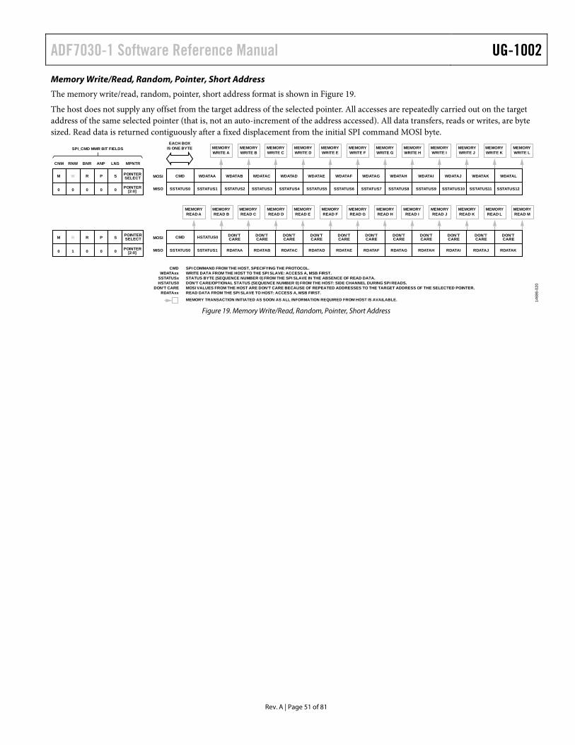
ADF7030-1 Software Reference Manual UG-1002
Rev. A | Page 51 of 81
Memory Write/Read, Random, Pointer, Short Address
The memory write/read, random, pointer, short address format is shown in Figure 19.
The host does not supply any offset from the target address of the selected pointer. All accesses are repeatedly carried out on the target address of the same selected pointer (that is, not an auto-increment of the address accessed). All data transfers, reads or writes, are byte sized. Read data is returned contiguously after a fixed displacement from the initial SPI command MOSI byte.
MPNTRLNSANP
SPI_CMD MMR BIT FIELDSEACH BOX
IS ONE BYTE
MOSI CMD
SSTATUS0
WDATAA
SPI COMMAND FROM THE HOST, SPECIFYING THE PROTOCOL.WRITE DATA FROM THE HOST TO THE SPI SLAVE: ACCESS A, MSB FIRST.STATUS BYTE (SEQUENCE NUMBER 0) FROM THE SPI SLAVE IN THE ABSENCE OF READ DATA.DON’T CARE/OPTIONAL STATUS (SEQUENCE NUMBER 0) FROM THE HOST: SIDE CHANNEL DURING SPI READS.MOSI VALUES FROM THE HOST ARE DON’T CARE BECAUSE OF REPEATED ADDRESSES TO THE TARGET ADDRESS OF THE SELECTED POINTER.READ DATA FROM THE SPI SLAVE TO HOST: ACCESS A, MSB FIRST.
MEMORY TRANSACTION INITIATED AS SOON AS ALL INFORMATION REQUIRED FROM HOST IS AVAILABLE.
HSTATUS0
CMDWDATAxx
SSTATUSxHSTATUS0
DON’T CARERDATAxx
SSTATUS1 SSTATUS2
WDATAB
SSTATUS3
WDATAC
SSTATUS4
WDATAD WDATAE
SSTATUS5 SSTATUS6 SSTATUS7 SSTATUS8 SSTATUS9 SSTATUS12SSTATUS10 SSTATUS11
WDATAF WDATAG WDATAH WDATAK WDATALWDATAI WDATAJ
MISO
BNRRNWCNM
M W R P S
0 0 0 0 0 POINTER[2:0]
POINTER[2:0]
POINTERSELECT
MOSI CMD
SSTATUS0 SSTATUS1 RDATAB RDATAC RDATAD RDATAE RDATAFRDATAA RDATAI RDATAJ RDATAKRDATAG RDATAHMISO
M R R P S
0 1 0 0 0
POINTERSELECT
MEMORYREAD G
MEMORYREAD A
MEMORYREAD H
MEMORYREAD B
MEMORYREAD I
MEMORYREAD C
MEMORYREAD J
MEMORYREAD K
MEMORYREAD L
MEMORYREAD M
MEMORYREAD D
MEMORYREAD E
MEMORYREAD F
MEMORYWRITE G
MEMORYWRITE A
MEMORYWRITE H
MEMORYWRITE B
MEMORYWRITE I
MEMORYWRITE C
MEMORYWRITE J
MEMORYWRITE K
MEMORYWRITE L
MEMORYWRITE D
MEMORYWRITE E
MEMORYWRITE F
DON’TCARE
DON’TCARE
DON’TCARE
DON’TCARE
DON’TCARE
DON’TCARE
DON’TCARE
DON’TCARE
DON’TCARE
DON’TCARE
DON’TCARE
1468
6-02
0
Figure 19. Memory Write/Read, Random, Pointer, Short Address
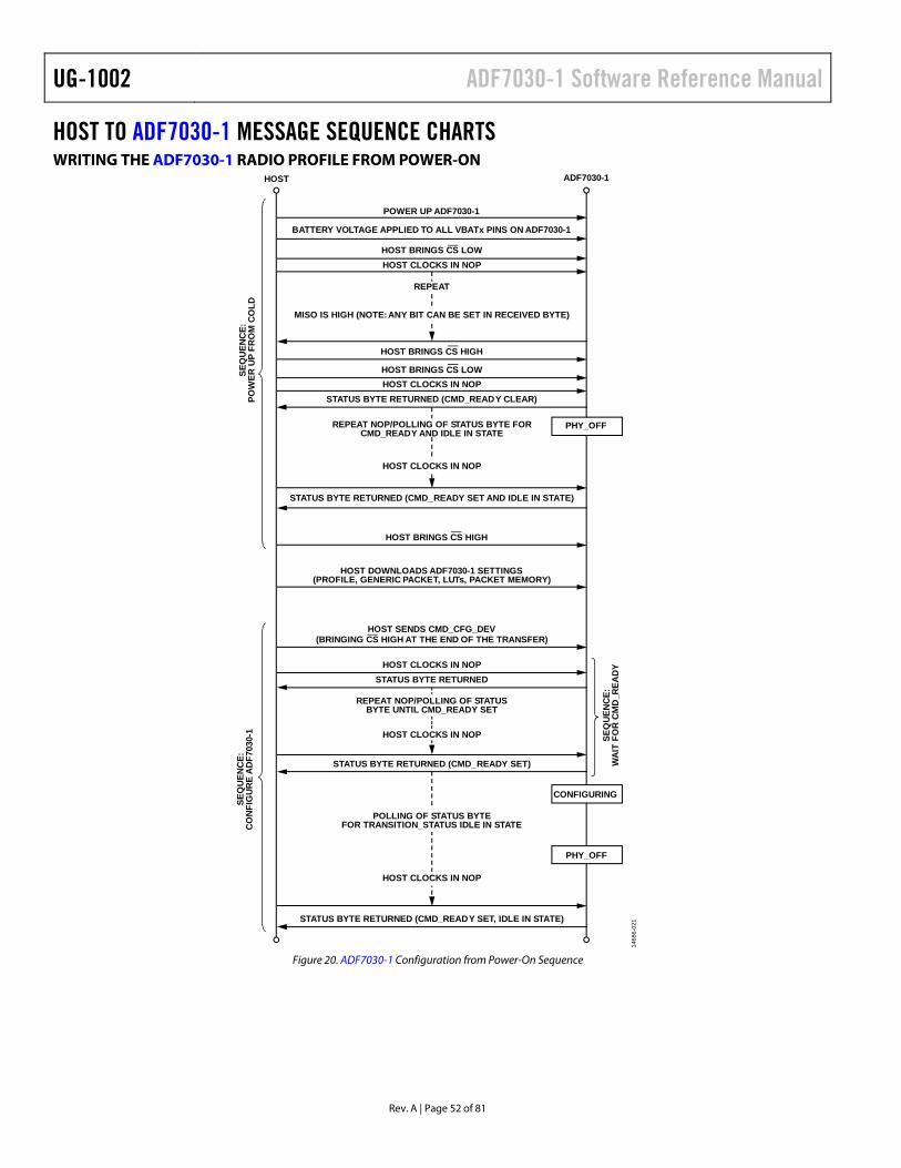
UG-1002 ADF7030-1 Software Reference Manual
Rev. A | Page 52 of 81
HOST TO ADF7030-1 MESSAGE SEQUENCE CHARTS WRITING THE ADF7030-1 RADIO PROFILE FROM POWER-ON
HOST ADF7030-1
HOST BRINGS CS LOW
BATTERY VOLTAGE APPLIED TO ALL VBATx PINS ON ADF7030-1
HOST CLOCKS IN NOP
HOST BRINGS CS HIGH
HOST DOWNLOADS ADF7030-1 SETTINGS(PROFILE, GENERIC PACKET, LUTs, PACKET MEMORY)
HOST SENDS CMD_CFG_DEV(BRINGING CS HIGH AT THE END OF THE TRANSFER)
HOST CLOCKS IN NOPHOST BRINGS CS LOW
STATUS BYTE RETURNED (CMD_READY CLEAR)
STATUS BYTE RETURNED (CMD_READY SET AND IDLE IN STATE)
HOST CLOCKS IN NOPSTATUS BYTE RETURNED
STATUS BYTE RETURNED (CMD_READY SET)
STATUS BYTE RETURNED (CMD_READY SET, IDLE IN STATE)
HOST BRINGS CS HIGH
POWER UP ADF7030-1
SEQ
UEN
CE:
POW
ER U
P FR
OM
CO
LDSE
QU
ENC
E:C
ON
FIG
UR
EA
DF7
030-
1
SEQ
UEN
CE:
WA
IT F
OR
CM
D_R
EAD
Y
REPEAT NOP/POLLING OF STATUSBYTE UNTIL CMD_READY SET
PHY_OFF
CONFIGURING
POLLING OF STATUS BYTEFOR TRANSITION_STATUS IDLE IN STATE
PHY_OFF
HOST CLOCKS IN NOP
HOST CLOCKS IN NOP
HOST CLOCKS IN NOP
REPEAT NOP/POLLING OF STATUS BYTE FORCMD_READY AND IDLE IN STATE
REPEAT
MISO IS HIGH (NOTE:ANY BIT CAN BE SET IN RECEIVED BYTE)
1468
6-02
1
Figure 20. ADF7030-1 Configuration from Power-On Sequence

ADF7030-1 Software Reference Manual UG-1002
Rev. A | Page 53 of 81
TRANSMITTING A SINGLE PACKET FROM POWER-OFF HOST ADF7030-1
HOST SENDS CMD_PHY_ON(BRINGING CS HIGH AT THE END OF THE TRANSFER)
HOST CLOCKS IN NOP
TRANSMITPACKET
HOST SENDS CMD_PHY_TX(BRINGING CS HIGH AT THE END OF THE TRANSFER)
HOST CLOCKS IN NOPSTATUS BYTE RETURNED
(CMD_READY SET, EXECUTING IN A STATE)
PACKETTRANSMITTED
POLLING OF STATUS BYTE FORTRANSITION_STATUS IDLE IN STATE
IRQ EVENTS CLEARED
POLLING OF STATUS BYTE FORTRANSITION_STATUS IDLE IN STATE
GENERIC PACKET FIELDS OPTIONALLY UPDATEDPACKET DATA TO BE TRANSMITTED OPTIONALLY UPDATED
CHANNEL FREQUENCY OPTIONALLY UPDATED HERE
SEQ
UEN
CE:
Tx
HOST DOWNLOADS ADF7030-1 SETTINGS AND PACKETTO BE TRANSMITTED
SEQUENCE: POWER UP FROM COLD
SEQUENCE: CONFIGURE ADF7030-1
PHY_OFF
PHY_TX
PHY_ON
PHY_ON
PHY_OFF
PHY_OFF
SEQ
UEN
CE:
GO
TO P
HY_
ON
STATUS BYTE RETURNED (CMD_READY SET, IDLE IN A STATE)
SEQUENCE: WAIT FOR CMD_READY
SEQUENCE: WAIT FOR CMD_READY
IRQ SET AS ENABLED EVENTS OCCUR(FOR EXAMPLE, PREAMBLE SENT, SYNC SENT, CRC GONE)
HOST CLOCKS IN NOP
STATUS BYTE RETURNED(CMD_READY SET, IDLE IN A STATE)
1468
6-02
2
Figure 21. Transmit a Packet from Power-Off Sequence

UG-1002 ADF7030-1 Software Reference Manual
Rev. A | Page 54 of 81
RECEIVING A SINGLE PACKET FROM POWER-OFF
HOST ADF7030-1
SEQ
UEN
CE:
Rx
RECEIVE APACKET
HOST SENDS CMD_PHY_RX(BRINGING CS HIGH AT THE END OF THE TRANSFER)
HOST CLOCKS IN NOP
STATUS BYTE RETURNED(CMD_READY SET, EXECUTING IN A STATE)
PACKET RECEIVEDBY ADF7030-1IRQ EVENTS CLEARED
GENERIC PACKET FIELDS OPTIONALLY UPDATEDCHANNEL FREQUENCY OPTIONALLY UPDATED
RECEIVEDPACKET DATA
HOST READS RECEIVED PACKET DATAWITH MEMORY ACCESS COMMANDS
PACKET DATA RETURNED
HOST DOWNLOADS ADF7030-1 SETTINGS
PHY_ON
PHY_RX
PHY_ON
PHY_ON
PHY_OFF
PHY_OFF
POLLING OF STATUS BYTE FORTRANSITION_STATUS IDLE IN STATE
HOST CLOCKS IN NOP
SEQUENCE: CONFIGURE ADF7030-1
SEQUENCE: GO TO PHY_ON
SEQUENCE: POWER UP FROM COLD
SEQUENCE: WAIT FOR CMD_READY
IRQ SET AS ENABLED EVENTS OCCUR(FOR EXAMPLE, PREAMBLE DETECT PREAMBLE DETECT,
SYNC DETECT, CRC CORRECT)
STATUS BYTE RETURNED(CMD_READY SET, IDLE IN A STATE)
1468
6-02
3
Figure 22. Receive a Packet from Cold Start
ADF7030-1 Software Reference Manual UG-1002
Rev. A | Page 55 of 81
CALIBRATION FIRMWARE MODULE, HOST SAVING ADF7030-1 CALIBRATION RESULTS
HOST ADF7030-1
SEQ
UEN
CE:
EXEC
UTE
CA
LIB
RA T
ION
FW
MO
DU
LE
HOST SENDS CMD_DO_CAL(BRINGING CS HIGH AT THE END OF THE TRANSFER)
HOST CLOCKS IN NOPs
HOST READS AND SAVES CALIBRATION RESULTS
POLLING OF STATUS BYTE FORTRANSITION_STATUS IDLE IN STATE
SEQUENCE: GO TO PHY_ON
SEQUENCE: WAIT FOR CMD_READY
NEXT, HOST DOWNLOADS OFFLINE CALIBRATIONS MODULE
ENSURE ADF7030-1 IS CONFIGURED
PHY_ON
CALIBRATING
PHY_ON
PHY_OFF
PHY_OFF
STATUS BYTE RETURNED (CMD_READY SET, IDLE IN A STATE)
1468
6-02
4
Figure 23. System Calibration Using Firmware Module
Rx IMMEDIATELY FOLLOWING CALIBRATION HOST ADF7030-1
RECEIVEPACKET
PACKETRECEIVED
CALIBRATEADF7030-1
SEQUENCE: EXECUTE CALIBRATION FW MODULE
SEQUENCE: Rx
CALIBRATIONCOMPLETE
PHY_ON
PHY_OFF
PHY_OFF
1468
6-02
5
Figure 24. Packet Reception Immediately Following a Calibration
UG-1002 ADF7030-1 Software Reference Manual
Rev. A | Page 56 of 81
Rx WITH CACHED CALIBRATION DATA HOST ADF7030-1
RECEIVEPACKET
PACKETRECEIVED
SEQUENCE: Rx
SEQUENCE: CONFIGURE ADF7030-1
SEQUENCE: POWER UP FROM COLD
HOST DOWNLOADS ADF7030-1 SETTINGS
HOST DOWNLOADS ADF7030-1CALIBRATION RESULTS FROM LAST CALIBRATION
PHY_ON
PHY_OFF
PHY_OFF
1468
6-02
6
Figure 25. Packet Reception from Cold Start with Saved Calibration Results

ADF7030-1 Software Reference Manual UG-1002
Rev. A | Page 57 of 81
REGISTER SUMMARY: ADF7030-1 Table 26. ADF7030-1 State Machine Summary Address Name Description
0x200000E4 SM_CONFIG_WAKE_SOURCE State machine wake source
0x200000FC SM_CONFIG_GPIO_CMD_0 State machine command triggered by IRQ_IN0
0x200000FE SM_CONFIG_GPIO_CMD_1 State machine command triggered by IRQ_IN1
0x20000130 SM_DATA_CALIBRATION State machine control for calibration
Table 27. ADF7030-1 Register Summary Address Name Description 0x200002E4 PROFILE_XTAL_CFG XTAL configuration. 0x200002E8 PROFILE_REF_CLK_CFG Reference clock configuration. 0x200002EC PROFILE_CH_FREQ RF channel frequency. 0x200002F0 PROFILE_IF Intermediate frequency. 0x200002F4 PROFILE_PACKET_CFG Packet handler configuration. 0x200002F8 PROFILE_RADIO_MODES Radio mode configuration. 0x200002FC PROFILE_RADIO_DATA_RATE Data rate configuration. 0x20000300 PROFILE_RADIO_DIG_RX_CFG Rx configuration. 0x20000304 PROFILE_RADIO_DIG_TX_CFG0 Tx Configuration 0. 0x20000308 PROFILE_RADIO_DIG_TX_CFG1 Tx Configuration 1. 0x2000030C PROFILE_RADIO_DIG_TX_CFG2 Tx Configuration 2. 0x20000310 PROFILE_RADIO_CDR_CFG Clock data recovery (CDR) configuration. 0x20000314 PROFILE_RADIO_PLL_CFG Phase-locked loop (PLL) configuration. 0x20000318 PROFILE_RADIO_AFC_CFG0 Automatic Frequency Control (AFC) Configuration Register 0. 0x2000031C PROFILE_RADIO_AFC_CFG1 AFC Configuration Register 1. 0x20000320 PROFILE_RADIO_AFC_CFG2 AFC Configuration Register 2. 0x20000324 PROFILE_RADIO_AGC_CFG0 Automatic Gain Control (AGC) Configuration Register 0. 0x20000328 PROFILE_RADIO_AGC_CFG1 AGC Configuration Register 1. 0x2000032C PROFILE_RADIO_AGC_CFG2 AGC Configuration Register 2. 0x20000330 PROFILE_RADIO_AGC_CFG3 AGC Configuration Register 3. 0x20000334 PROFILE_RADIO_AGC_CFG4 AGC Configuration Register 4. 0x20000338 PROFILE_RADIO_AGC_CFG5 AGC Configuration Register 5. 0x2000033C PROFILE_RADIO_AGC_CFG6 AGC Configuration Register 6. 0x20000340 PROFILE_RADIO_AGC_CFG7 AGC Configuration Register 7. 0x20000344 PROFILE_RADIO_AGC_CFG8 AGC Configuration Register 8. 0x20000348 PROFILE_OCL_CFG0 Open Control Loop Configuration 0. 0x2000034C PROFILE_OCL_CFG1 Open Control Loop Configuration 1. 0x20000350 PROFILE_RADIO_VCO_CFG0 VCO Configuration 0. 0x20000354 PROFILE_RADIO_VCO_CFG1 VCO Configuration 1. 0x20000358 PROFILE_RADIO_ANC_CFG0 Ancillary PLL Configuration 0. 0x2000035C PROFILE_RADIO_ANC_CFG1 Ancillary PLL Configuration 1. 0x20000360 PROFILE_RADIO_LUT_CFG Lookup table configuration. 0x20000364 PROFILE_RADIO_LUT_PTR Lookup table pointer. 0x20000368 PROFILE_RADIO_CAL_CFG0 Calibration Configuration 0. 0x2000036C PROFILE_RADIO_CAL_CFG1 Calibration Configuration 1. 0x20000370 PROFILE_RADIO_CAL_CFG2 Calibration Configuration 2. 0x20000374 PROFILE_RSSI_CFG RSSI configuration. 0x20000378 PROFILE_CCA_CFG CCA configuration. 0x2000037C PROFILE_CCA_READBACK CCA readback. 0x20000380 PROFILE_LPM_CFG0 Low power mode configuration. 0x20000384 PROFILE_LPM_CFG1 RTC configuration. 0x20000388 PROFILE_MONITOR0 Monitor configuration.

UG-1002 ADF7030-1 Software Reference Manual
Rev. A | Page 58 of 81
Address Name Description 0x2000038C PROFILE_MONITOR1 Monitor readback. 0x20000390 PROFILE_MISC0 Miscellaneous configuration. 0x20000394 PROFILE_GPCON0_3 GPIO0 to GPIO3 pin functionality selection. 0x20000398 PROFILE_GPCON4_7 GPIO4 to GPIO7 pin functionality selection. 0x2000039C PROFILE_GPIO_CFG GPIOx pin configuration. 0x200003A0 PROFILE_SPARE0 Spare Register 0. 0x200003A4 PROFILE_SPARE1 Spare Register 1. 0x200003A8 PROFILE_SPARE2 Spare Register 2. 0x200003AC PROFILE_SPARE3 Spare Register 3. 0x200003B0 PROFILE_SPARE4 Spare Register 4. 0x200003B4 PROFILE_SPARE5 Spare Register 5. 0x200003B8 PROFILE_SPARE6 Spare Register 6. 0x200003BC PROFILE_SPARE7 Spare Register 7. 0x200003C0 PROFILE_SPARE8 Spare Register 8. 0x200003C4 PROFILE_SPARE9 Spare Register 9. 0x200003C8 PROFILE_RADIO_CAL_RESULTS0 Radio Calibration Results 0. 0x200003CC PROFILE_RADIO_CAL_RESULTS1 Radio Calibration Results 1. 0x200003D0 PROFILE_RADIO_CAL_RESULTS2 Radio Calibration Results 2. 0x200003D4 PROFILE_RADIO_CAL_RESULTS3 Radio Calibration Results 3. 0x200003D8 PROFILE_RADIO_CAL_RESULTS4 Radio Calibration Results 4. 0x200003DC PROFILE_RADIO_CAL_RESULTS5 Radio Calibration Results 5. 0x200003E0 PROFILE_RADIO_CAL_RESULTS6 Radio Calibration Results 6. 0x200003E4 PROFILE_RADIO_CAL_RESULTS7 Radio Calibration Results 7. 0x200003E8 PROFILE_RADIO_CAL_RESULTS8 Radio Calibration Results 8. 0x200004F4 GENERIC_PKT_BUFF_CFG0 Transmit/Receive Buffer Configuration 0. 0x200004F8 GENERIC_PKT_BUFF_CFG1 Transmit/Receive Buffer Configuration 1. 0x200004FC GENERIC_PKT_FRAME_CFG0 Generic Packet Frame Configuration 0. 0x20000500 GENERIC_PKT_FRAME_CFG1 Generic Packet Frame Configuration 1. 0x20000504 GENERIC_PKT_FRAME_CFG2 Generic Packet Frame Configuration 2. 0x20000508 GENERIC_PKT_FRAME_CFG3 Generic Packet Frame Configuration 3. 0x2000050C GENERIC_PKT_FRAME_CFG4 Generic Packet Frame Configuration 4. 0x20000510 GENERIC_PKT_FRAME_CFG5 Generic Packet Frame Configuration 5. 0x20000514 GENERIC_PKT_SYNCWORD0 Sync Word 0. 0x20000518 GENERIC_PKT_SYNCWORD1 Sync Word 1. 0x2000051C GENERIC_PKT_CRC_POLY CRC polynomial. 0x20000520 GENERIC_PKT_CRC_SEED CRC initial seed. 0x20000524 GENERIC_PKT_CRC_FINAL_XOR CRC XOR value. 0x20000528 GENERIC_PKT_LOCK_CFG Rx lock configuration. 0x2000052C GENERIC_PKT_TICK_CFG RSSI configuration. 0x20000530 GENERIC_PKT_SEARCH_DETECT Packet detection configuration. 0x20000534 GENERIC_PKT_SEARCH_QUAL Packet qualification configuration. 0x20000538 GENERIC_PKT_LIVE_LINK_QUAL RX link quality readback. 0x2000053C GENERIC_PKT_MISC0 Miscellaneous Register 0. 0x20000540 GENERIC_PKT_MISC1 Miscellaneous Register 1. 0x20000544 GENERIC_PKT_LPM_CFG Low power mode configuration. 0x20000548 GENERIC_PKT_TEST_MODES0 Test Mode Configuration 0. 0x2000054C GENERIC_PKT_TEST_MODES1 Test Mode Configuration 1. 0x20000550 GENERIC_PKT_RESAMPLE_CFG Resample configuration. 0x20000554 GENERIC_PKT_MISC3 Miscellaneous Register 3. 0x20000558 GENERIC_PKT_MISC4 Miscellaneous Register 4. 0x2000055C GENERIC_PKT_MISC2 Miscellaneous Register 2. 0x20000560 GENERIC_PKT_MISC5 Miscellaneous Register 5. 0x2000060C ANAFILT_LUTS_DATA0 Analog filter LUTs in RAM. Generated by the ADF7030-1 design center.

ADF7030-1 Software Reference Manual UG-1002
Rev. A | Page 59 of 81
Address Name Description 0x20000610 ANAFILT_LUTS_DATA1 Analog filter LUTs in RAM. Generated by the ADF7030-1 design center. 0x20000614 ANAFILT_LUTS_DATA2 Analog filter LUTs in RAM. Generated by the ADF7030-1 design center. 0x20000618 ANAFILT_LUTS_DATA3 Analog filter LUTs in RAM. Generated by the ADF7030-1 design center. 0x2000061C ANAFILT_LUTS_DATA4 Analog filter LUTs in RAM. Generated by the ADF7030-1 design center. 0x20000620 ANAFILT_LUTS_DATA5 Analog filter LUTs in RAM. Generated by the ADF7030-1 design center. 0x20000624 ANAFILT_LUTS_DATA6 Analog filter LUTs in RAM. Generated by the ADF7030-1 design center. 0x20000628 ANAFILT_LUTS_DATA7 Analog filter LUTs in RAM. Generated by the ADF7030-1 design center. 0x2000062C ANAFILT_LUTS_DATA8 Analog filter LUTs in RAM. Generated by the ADF7030-1 design center. 0x20000630 ANAFILT_LUTS_DATA9 Analog filter LUTs in RAM. Generated by the ADF7030-1 design center. 0x20000634 ANAFILT_LUTS_DATA10 Analog filter LUTs in RAM. Generated by the ADF7030-1 design center. 0x20000638 ANAFILT_LUTS_DATA11 Analog filter LUTs in RAM. Generated by the ADF7030-1 design center. 0x2000063C ANAFILT_LUTS_DATA12 Analog filter LUTs in RAM. Generated by the ADF7030-1 design center. 0x200006B4 DIGFILT_LUTS_DATA0 Digital filter LUTs in RAM. Generated by the ADF7030-1 design center. 0x200006B8 DIGFILT_LUTS_DATA1 Digital filter LUTs in RAM. Generated by the ADF7030-1 design center. 0x200006BC DIGFILT_LUTS_DATA2 Digital filter LUTs in RAM. Generated by the ADF7030-1 design center. 0x200006C0 DIGFILT_LUTS_DATA3 Digital filter LUTs in RAM. Generated by the ADF7030-1 design center. 0x200006C4 DIGFILT_LUTS_DATA4 Digital filter LUTs in RAM. Generated by the ADF7030-1 design center. 0x200006C8 DIGFILT_LUTS_DATA5 Digital filter LUTs in RAM. Generated by the ADF7030-1 design center. 0x200006CC DIGFILT_LUTS_DATA6 Digital filter LUTs in RAM. Generated by the ADF7030-1 design center. 0x200006D0 DIGFILT_LUTS_DATA7 Digital filter LUTs in RAM. Generated by the ADF7030-1 design center. 0x200006D4 DIGFILT_LUTS_DATA8 Digital filter LUTs in RAM. Generated by the ADF7030-1 design center. 0x200006D8 DIGFILT_LUTS_DATA9 Digital filter LUTs in RAM. Generated by the ADF7030-1 design center. 0x200006DC DIGFILT_LUTS_DATA10 Digital filter LUTs in RAM. Generated by the ADF7030-1 design center. 0x200006E0 DIGFILT_LUTS_DATA11 Digital filter LUTs in RAM. Generated by the ADF7030-1 design center. 0x200006E4 DIGFILT_LUTS_DATA12 Digital filter LUTs in RAM. Generated by the ADF7030-1 design center. 0x200006E8 DIGFILT_LUTS_DATA13 Digital filter LUTs in RAM. Generated by the ADF7030-1 design center. 0x200006EC DIGFILT_LUTS_DATA14 Digital filter LUTs in RAM. Generated by the ADF7030-1 design center. 0x200006F0 DIGFILT_LUTS_DATA15 Digital filter LUTs in RAM. Generated by the ADF7030-1 design center. 0x200006F4 DIGFILT_LUTS_DATA16 Digital filter LUTs in RAM. Generated by the ADF7030-1 design center. 0x20000794 DIGFILT2_LUTS_DATA0 Digital Filter 2 LUTs in RAM. Generated by the ADF7030-1 design center. 0x20000798 DIGFILT2_LUTS_DATA1 Digital Filter 2 LUTs in RAM. Generated by the ADF7030-1 design center. 0x2000079C DIGFILT2_LUTS_DATA2 Digital Filter 2 LUTs in RAM. Generated by the ADF7030-1 design center. 0x200007A0 DIGFILT2_LUTS_DATA3 Digital Filter 2 LUTs in RAM. Generated by the ADF7030-1 design center. 0x200007A4 DIGFILT2_LUTS_DATA4 Digital Filter 2 LUTs in RAM. Generated by the ADF7030-1 design center. 0x200007A8 DIGFILT2_LUTS_DATA5 Digital Filter 2 LUTs in RAM. Generated by the ADF7030-1 design center. 0x200007AC DIGFILT2_LUTS_DATA6 Digital Filter 2 LUTs in RAM. Generated by the ADF7030-1 design center. 0x200007B0 DIGFILT2_LUTS_DATA7 Digital Filter 2 LUTs in RAM. Generated by the ADF7030-1 design center. 0x200007B4 DIGFILT2_LUTS_DATA8 Digital Filter 2 LUTs in RAM. Generated by the ADF7030-1 design center. 0x200007B8 DIGFILT2_LUTS_DATA9 Digital Filter 2 LUTs in RAM. Generated by the ADF7030-1 design center. 0x200007BC DIGFILT2_LUTS_DATA10 Digital Filter 2 LUTs in RAM. Generated by the ADF7030-1 design center. 0x20000820 PLLBW_LUTS_DATA0 PLL Bandwidth LUTs in RAM. Generated by the ADF7030-1 design
center. 0x20000824 PLLBW_LUTS_DATA1 PLL Bandwidth LUTs in RAM. Generated by the ADF7030-1 design
center. 0x20000844 VCO_CAL_RESULTS_DATA0 VCO calibration results LUT in RAM. 0x20000848 VCO_CAL_RESULTS_DATA1 VCO calibration results LUT in RAM. 0x2000084C VCO_CAL_RESULTS_DATA2 VCO calibration results LUT in RAM. 0x20000850 VCO_CAL_RESULTS_DATA3 VCO calibration results LUT in RAM. 0x20000854 VCO_CAL_RESULTS_DATA4 VCO calibration results LUT in RAM. 0x20000858 VCO_CAL_RESULTS_DATA5 VCO calibration results LUT in RAM. 0x2000085C VCO_CAL_RESULTS_DATA6 VCO calibration results LUT in RAM. 0x20000860 VCO_CAL_RESULTS_DATA7 VCO calibration results LUT in RAM. 0x20000864 RSSICFG_LUTS_DATA0 RSSI LUTs in RAM. Generated by the ADF7030-1 design center. 0x20000868 RSSICFG_LUTS_DATA1 RSSI LUTs in RAM. Generated by the ADF7030-1 design center.

UG-1002 ADF7030-1 Software Reference Manual
Rev. A | Page 60 of 81
Address Name Description 0x2000086C RSSICFG_LUTS_DATA2 RSSI LUTs in RAM. Generated by the ADF7030-1 design center. 0x20000870 RSSICFG_LUTS_DATA3 RSSI LUTs in RAM. Generated by the ADF7030-1 design center. 0x20000874 RSSICFG_LUTS_DATA4 RSSI LUTs in RAM. Generated by the ADF7030-1 design center. 0x20000878 RSSICFG_LUTS_DATA5 RSSI LUTs in RAM. Generated by the ADF7030-1 design center. 0x2000087C RSSICFG_LUTS_DATA6 RSSI LUTs in RAM. Generated by the ADF7030-1 design center. 0x20000880 RSSICFG_LUTS_DATA7 RSSI LUTs in RAM. Generated by the ADF7030-1 design center. 0x20000884 RSSICFG_LUTS_DATA8 RSSI LUTs in RAM. Generated by the ADF7030-1 design center. 0x20000888 RSSICFG_LUTS_DATA9 RSSI LUTs in RAM. Generated by the ADF7030-1 design center. 0x2000088C RSSICFG_LUTS_DATA10 RSSI LUTs in RAM. Generated by the ADF7030-1 design center. 0x20000890 RSSICFG_LUTS_DATA11 RSSI LUTs in RAM. Generated by the ADF7030-1 design center. 0x20000894 RSSICFG_LUTS_DATA12 RSSI LUTs in RAM. Generated by the ADF7030-1 design center. 0x20000898 RSSICFG_LUTS_DATA13 RSSI LUTs in RAM. Generated by the ADF7030-1 design center. 0x2000089C RSSICFG_LUTS_DATA14 RSSI LUTs in RAM. Generated by the ADF7030-1 design center. 0x40000C08 PMU_KEY Gateway for software keyed instructions. 0x40000C20 PMU_CLOCKS PMU clock control register. 0x40001800 SPI_HOST_PNTR0 SPI Slave Pointer 0. 0x40001804 SPI_HOST_PNTR1 SPI Slave Pointer 1. 0x40001808 SPI_HOST_PNTR2 SPI Slave Pointer 2. 0x40003800 IRQ_CTRL_MASK0 Mask for External Interrupt 0 (IRQ_OUT0). 0x40003804 IRQ_CTRL_MASK1 Mask for External Interrupt 1 (IRQ_OUT1). 0x40003808 IRQ_CTRL_STATUS0 External Interrupt 0 (IRQ_OUT0) status. 0x4000380C IRQ_CTRL_STATUS1 External Interrupt 1 (IRQ_OUT1) status. 0x400041F8 AFC_CONFIG AFC configuration. 0x40004208 AFC_FREQUENCY_ERROR AFC frequency error readback. 0x40004278 CRMGT_PROC_CLK_EN Processor clock enable. 0x400042B4 MISC_FW Firmware status and debug.

ADF7030-1 Software Reference Manual UG-1002
Rev. A | Page 61 of 81
REGISTER DETAILS: ADF7030-1 Registers that contain user visible fields are detailed in this section. Unless noted otherwise, when writing to a bit field within a register, the other bits must be preserved.
STATE MACHINE WAKE SOURCE Address: 0x200000E4: SM_CONFIG_WAKE_SOURCE
Table 28. Bit Descriptions for SM_CONFIG_WAKE_SOURCE Bits Bit Name Settings Description [31:24] EXT 1 IRQ0.
10 IRQ1.
100 RTC.
[23:16] IRQ 100 CSN low.
[15:0] RESERVED Reserved.
STATE MACHINE COMMAND TRIGGERED BY IRQ_IN0 REGISTER Address: 0x200000FC, Name: SM_CONFIG_GPIO_CMD_0
Table 29. Bit Descriptions for SM_CONFIG_GPIO_CMD_0 Bits Bit Name Settings Description
[7:0] VAL State machine command triggered by IRQ_IN0
STATE MACHINE COMMAND TRIGGERED BY IRQ_IN1 REGISTER Address: 0x200000FE, Name: SM_CONFIG_GPIO_CMD_1
Table 30. Bit Descriptions for SM_CONFIG_GPIO_CMD_1 Bits Bit Name Settings Description
[7:0] VAL State machine command triggered by IRQ_IN1
STATE MACHINE CONTROL FOR CALIBRATION Address: 0x20000130, Name: SM_DATA_CALIBRATION
Table 31. Bit Descriptions for SM_DATA_CALIBRATION Bits Bit Name Settings Description
[31:0] VAL Enable or disable the offline calibration.
0x20002971 CAL_ENABLE key. Enable the calibration.
0x20002A21 CAL_DISABLE key. Disable the calibration.
REFERENCE CLOCK CONFIGURATION REGISTER Address: 0x200002E8, Name: PROFILE_REF_CLK_CFG
Table 32. Bit Descriptions for PROFILE_REF_CLK_CFG Bits Bit Name Settings Description
[31:27] GENERATED Generated by the ADF7030-1 design center.

UG-1002 ADF7030-1 Software Reference Manual
Rev. A | Page 62 of 81
Bits Bit Name Settings Description
26 CLK_TYPE External reference clock source type.
0 TCXO selected.
1 XTAL selected.
[25:0] GENERATED Generated by the ADF7030-1 design center.
RF CHANNEL FREQUENCY REGISTER Address: 0x200002EC, Name: PROFILE_CH_FREQ
Table 33. Bit Descriptions for PROFILE_CH_FREQ Bits Bit Name Settings Description
[31:0] VAL Channel frequency in Hz
PACKET HANDLER CONFIGURATION REGISTER Address: 0x200002F4, Name: PROFILE_PACKET_CFG
Table 34. Bit Descriptions for PROFILE_PACKET_CFG Bits Bit Name Settings Description
[31:16] GENERATED Generated by the ADF7030-1 design center.
[15:14] TYPE_FRAME0 Select the packet format.
0 Generic packet format.
1 IEEE 802.15.4g packet format.
[13:0] GENERATED Generated by the ADF7030-1 design center.
RADIO MODE CONFIGURATION REGISTER Address: 0x200002F8, Name: PROFILE_RADIO_MODES
Table 35. Bit Descriptions for PROFILE_RADIO_MODES Bits Bit Name Settings Description
[31:27] RESERVED Bits set to 0.
[26:22] RESERVED Reserved.
[21:19] GPIO_CLK_FREQ_SEL Selection of clock frequency on selected GPIO with CMD_GPCLK command.
000 6.5 MHz.
001 3.25 MHz.
010 1.625 MHz.
011 0.8125 MHz.
100 0.40625 MHz.
101 0.203125 MHz.
110 0.1015625 MHz.
111 0.05078125 MHz.
[18:7] RESERVED Reserved.
[6:5] COMBINED_TRX_MATCH Combined match configuration.
1 Enable combined match.
0 Disable combined match.
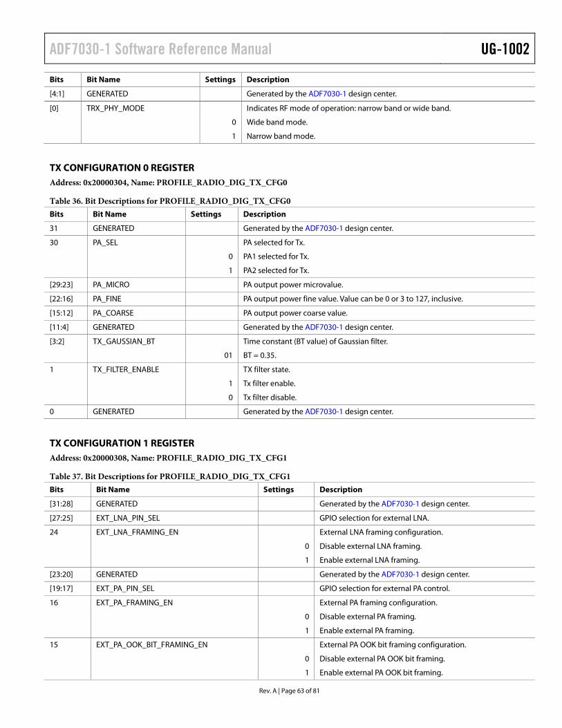
ADF7030-1 Software Reference Manual UG-1002
Rev. A | Page 63 of 81
Bits Bit Name Settings Description
[4:1] GENERATED Generated by the ADF7030-1 design center.
[0] TRX_PHY_MODE Indicates RF mode of operation: narrow band or wide band.
0 Wide band mode.
1 Narrow band mode.
TX CONFIGURATION 0 REGISTER Address: 0x20000304, Name: PROFILE_RADIO_DIG_TX_CFG0
Table 36. Bit Descriptions for PROFILE_RADIO_DIG_TX_CFG0 Bits Bit Name Settings Description
31 GENERATED Generated by the ADF7030-1 design center.
30 PA_SEL PA selected for Tx.
0 PA1 selected for Tx.
1 PA2 selected for Tx.
[29:23] PA_MICRO PA output power microvalue.
[22:16] PA_FINE PA output power fine value. Value can be 0 or 3 to 127, inclusive.
[15:12] PA_COARSE PA output power coarse value.
[11:4] GENERATED Generated by the ADF7030-1 design center.
[3:2] TX_GAUSSIAN_BT Time constant (BT value) of Gaussian filter.
01 BT = 0.35.
1 TX_FILTER_ENABLE TX filter state.
1 Tx filter enable.
0 Tx filter disable.
0 GENERATED Generated by the ADF7030-1 design center.
TX CONFIGURATION 1 REGISTER Address: 0x20000308, Name: PROFILE_RADIO_DIG_TX_CFG1
Table 37. Bit Descriptions for PROFILE_RADIO_DIG_TX_CFG1 Bits Bit Name Settings Description
[31:28] GENERATED Generated by the ADF7030-1 design center.
[27:25] EXT_LNA_PIN_SEL GPIO selection for external LNA.
24 EXT_LNA_FRAMING_EN External LNA framing configuration.
0 Disable external LNA framing.
1 Enable external LNA framing.
[23:20] GENERATED Generated by the ADF7030-1 design center.
[19:17] EXT_PA_PIN_SEL GPIO selection for external PA control.
16 EXT_PA_FRAMING_EN External PA framing configuration.
0 Disable external PA framing.
1 Enable external PA framing.
15 EXT_PA_OOK_BIT_FRAMING_EN External PA OOK bit framing configuration.
0 Disable external PA OOK bit framing.
1 Enable external PA OOK bit framing.

UG-1002 ADF7030-1 Software Reference Manual
Rev. A | Page 64 of 81
Bits Bit Name Settings Description
[14:12] PA_RAMP_RATE Internal PA ramp rate.
[11:0] GENERATED Generated by the ADF7030-1 design center.
TX CONFIGURATION 2 REGISTER Address: 0x2000030C, Name: PROFILE_RADIO_DIG_TX_CFG2
Table 38. Bit Descriptions for PROFILE_RADIO_DIG_TX_CFG2 Bits Bit Name Settings Description
[31:4] GENERATED Generated by the ADF7030-1 design center.
[3:0] PAOLDO_VOUT_CON LDO output voltage regulator trim voltage.
1111 2.60 V.
1110 2.55 V.
1101 2.50 V.
1100 2.45 V.
1011 2.40 V.
1010 2.35 V.
1001 2.30 V.
1000 2.25 V.
0111 2.20 V.
0110 2.15 V.
0101 2.10 V.
0100 2.05 V.
0011 2.0 V.
0010 1.95 V.
0001 1.90 V.
0000 1.85 V.
AFC CONFIGURATION REGISTER 2 Address: 0x20000320, Name: PROFILE_RADIO_AFC_CFG2
Table 39. Bit Descriptions for PROFILE_RADIO_AFC_CFG2 Bits Bit Name Settings Description
[31:3] GENERATED Generated by the ADF7030-1 design center.
[2:0] AFC_MODE AFC mode.
0 AFC is disabled.
CALIBRATION CONFIGURATION 0 REGISTER Address: 0x20000368, Name: PROFILE_RADIO_CAL_CFG0
Table 40. Bit Descriptions for PROFILE_RADIO_CAL_CFG0 Bits Bit Name Settings Description
[31:0] DATA Calibration control. Generated by the ADF7030-1 design center.

ADF7030-1 Software Reference Manual UG-1002
Rev. A | Page 65 of 81
CALIBRATION CONFIGURATION 1 REGISTER Address: 0x2000036C, Name: PROFILE_RADIO_CAL_CFG1
Table 41. Bit Descriptions for PROFILE_RADIO_CAL_CFG1 Bits Bit Name Settings Description
[31:30] GENERATED Generated by the ADF7030-1 design center.
29 CAL_SUCCESS Calibration status.
0 The calibration has not been completed.
1 The calibration has been completed.
[28:0] GENERATED Generated by the ADF7030-1 design center.
RSSI CONFIGURATION REGISTER Address: 0x20000374, Name: PROFILE_RSSI_CFG
Table 42. Bit Descriptions for PROFILE_RSSI_CFG Bits Bit Name Settings Description
[31:26] GENERATED Bits generated by ADF7030-1 GUI.
[25:16] NB_OFFSET Narrow-band RSSI offset in units of 0.25 dBm. The offset value is an unsigned 10-bit number.
[15:10] GENERATED Bits generated by ADF7030-1 GUI.
[9:0] WB_OFFSET Wideband RSSI offset in units of 0.36 dBm. The offset value is an unsigned 10-bit number.
CCA CONFIGURATION REGISTER Address: 0x20000378, Name: PROFILE_CCA_CFG
Table 43. Bit Descriptions for PROFILE_CCA_CFG Bits Bit Name Settings Description [31:27] GENERATED Generated by the ADF7030-1 design center. [26:16] THRESHOLD Signed 11-bit number representing the CCA RSSI threshold, in units of 0.25 dBm. [15:8] DETECTION_TIME The number of RSSI samples taken before CCA detection period ends. A value 0 implies infinity
mode, whereby the CCA live status is continually updated and the ADF7030-1 stays in the CCA state.
[7:4] TICK_POSTSCALAR Sets the number of CCA ticks between RSSI samples. [3:0] TICK_RATE This field sets the number of CCA ticks per Rx data bit period. 0x0 1× data rate. 0x2 2× data rate. 0x3 4× data rate. 0x4 8× data rate. 0x5 16× data rate. 0x6 32× data rate. 0x7 64× data rate. 0x8 128× data rate.
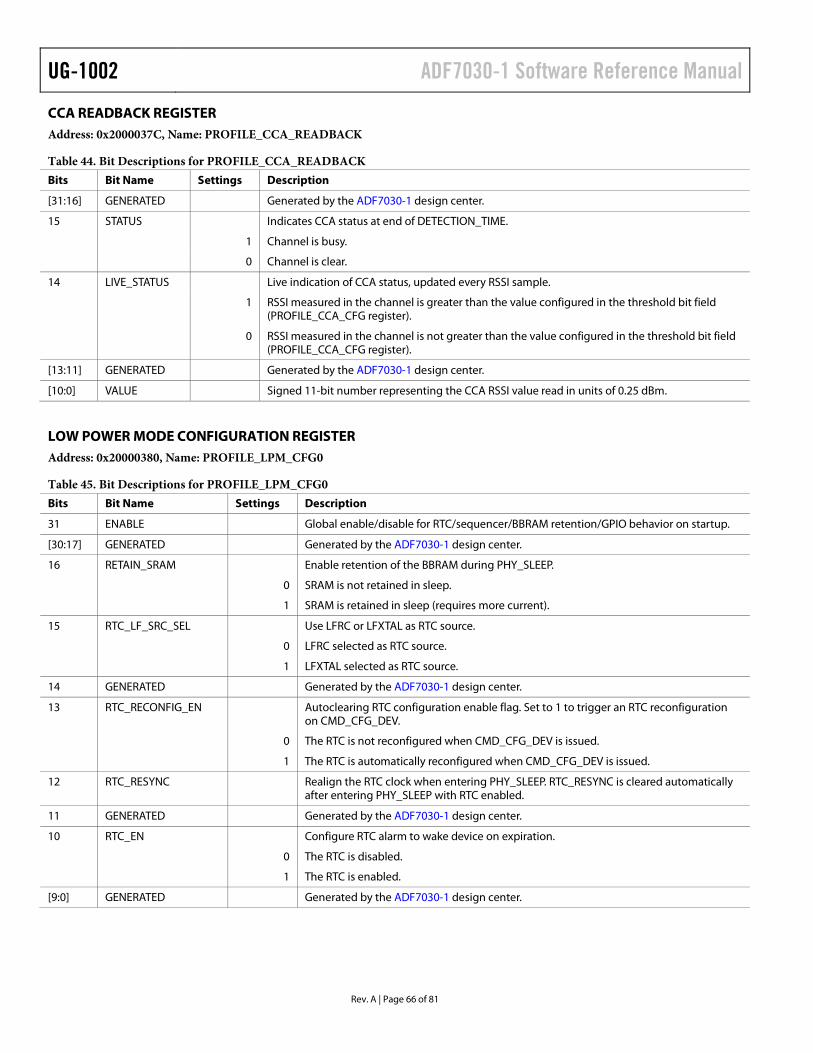
UG-1002 ADF7030-1 Software Reference Manual
Rev. A | Page 66 of 81
CCA READBACK REGISTER Address: 0x2000037C, Name: PROFILE_CCA_READBACK
Table 44. Bit Descriptions for PROFILE_CCA_READBACK Bits Bit Name Settings Description
[31:16] GENERATED Generated by the ADF7030-1 design center.
15 STATUS Indicates CCA status at end of DETECTION_TIME.
1 Channel is busy.
0 Channel is clear.
14 LIVE_STATUS Live indication of CCA status, updated every RSSI sample.
1 RSSI measured in the channel is greater than the value configured in the threshold bit field (PROFILE_CCA_CFG register).
0 RSSI measured in the channel is not greater than the value configured in the threshold bit field (PROFILE_CCA_CFG register).
[13:11] GENERATED Generated by the ADF7030-1 design center.
[10:0] VALUE Signed 11-bit number representing the CCA RSSI value read in units of 0.25 dBm.
LOW POWER MODE CONFIGURATION REGISTER Address: 0x20000380, Name: PROFILE_LPM_CFG0
Table 45. Bit Descriptions for PROFILE_LPM_CFG0 Bits Bit Name Settings Description
31 ENABLE Global enable/disable for RTC/sequencer/BBRAM retention/GPIO behavior on startup.
[30:17] GENERATED Generated by the ADF7030-1 design center.
16 RETAIN_SRAM Enable retention of the BBRAM during PHY_SLEEP.
0 SRAM is not retained in sleep.
1 SRAM is retained in sleep (requires more current).
15 RTC_LF_SRC_SEL Use LFRC or LFXTAL as RTC source.
0 LFRC selected as RTC source.
1 LFXTAL selected as RTC source.
14 GENERATED Generated by the ADF7030-1 design center.
13 RTC_RECONFIG_EN Autoclearing RTC configuration enable flag. Set to 1 to trigger an RTC reconfiguration on CMD_CFG_DEV.
0 The RTC is not reconfigured when CMD_CFG_DEV is issued.
1 The RTC is automatically reconfigured when CMD_CFG_DEV is issued.
12 RTC_RESYNC Realign the RTC clock when entering PHY_SLEEP. RTC_RESYNC is cleared automatically after entering PHY_SLEEP with RTC enabled.
11 GENERATED Generated by the ADF7030-1 design center.
10 RTC_EN Configure RTC alarm to wake device on expiration.
0 The RTC is disabled.
1 The RTC is enabled.
[9:0] GENERATED Generated by the ADF7030-1 design center.

ADF7030-1 Software Reference Manual UG-1002
Rev. A | Page 67 of 81
RTC CONFIGURATION REGISTER Address: 0x20000384, Name: PROFILE_LPM_CFG1
Table 46. Bit Descriptions for PROFILE_LPM_CFG1 Bits Bit Name Settings Description
[31:0] RTC_PERIOD Wake-up interval in units of RTC ticks (tick rate is dependent on source clock selected)
MONITOR READBACK REGISTER Address: 0x2000038C, Name: PROFILE_MONITOR1
Table 47. Bit Descriptions for PROFILE_MONITOR1 Bits Bit Name Settings Description
[31:12] RESERVED Bits set to 0.
[11:0] TEMP_OUTPUT Temperature as a signed 12-bit number in units of 0.0625°C.
GPIO0 TO GPIO3 PIN FUNCTIONALITY SELECTION REGISTER Address: 0x20000394, Name: PROFILE_GPCON0_3
Table 48. Bit Descriptions for PROFILE_GPCON0_3 Bits Bit Name Settings Description [31:30] RESERVED Bits set to 0. [29:24] PIN3_CFG GPIO3 configuration. 0x4 IRQ_IN0. Interrupt Input 0. 0x5 IRQ_IN1. Interrupt Input 1. 0x6 IRQ_OUT0. Interrupt Output 0. 0x7 IRQ_OUT1. Interrupt Output 1. 0xC SPORT_TXDATA. Serial port (SPORT) mode transmit data. 0xD SPORT_RXDATA. SPORT mode receive data. 0xE SPORT_TRXCLK. SPORT mode transmit/receive clock. 0x1B Set GPIO3 to output. 0x24 Programmable clock output (GPCLK_OUT state). [23:22] RESERVED Bits set to 0. [21:16] PIN2_CFG GPIO2 configuration. 0x4 IRQ_IN0. Interrupt Input 0. 0x5 IRQ_IN1. Interrupt Input 1. 0x6 IRQ_OUT0. Interrupt Output 0. 0x7 IRQ_OUT1. Interrupt Output 1. 0xC SPORT_TXDATA. SPORT mode transmit data. 0xD SPORT_RXDATA. SPORT mode receive data. 0xE SPORT_TRXCLK. SPORT mode transmit/receive clock. 0x1A Set GPIO2 to output. 0x24 Programmable clock output (GPCLK_OUT state). [15:14] RESERVED Bits set to 0. [13:8] PIN1_CFG GPIO1 configuration. 0x4 IRQ_IN0. Interrupt Input 0. 0x5 IRQ_IN1. Interrupt Input 1. 0x6 IRQ_OUT0. Interrupt Output 0. 0x7 IRQ_OUT1. Interrupt Output 1. 0xC SPORT_TXDATA. SPORT mode transmit data. 0xD SPORT_RXDATA. SPORT mode receive data. 0xE SPORT_TRXCLK. SPORT mode transmit/receive clock. 0x19 Set GPIO1 to output. 0x24 Programmable clock output (GPCLK_OUT state).

UG-1002 ADF7030-1 Software Reference Manual
Rev. A | Page 68 of 81
Bits Bit Name Settings Description [7:6] RESERVED Bits set to 0. [5:0] PIN0_CFG GPIO0 configuration. 0x4 IRQ_IN0. Interrupt Input 0. 0x5 IRQ_IN1. Interrupt Input 1. 0x6 IRQ_OUT0. Interrupt Output 0. 0x7 IRQ_OUT1. Interrupt Output 1. 0xC SPORT_TXDATA. SPORT mode transmit data. 0xD SPORT_RXDATA. SPORT mode receive data. 0xE SPORT_TRXCLK. SPORT mode transmit/receive clock. 0x18 Set GPIO0 to output. 0x24 Programmable clock output (GPCLK_OUT state).
GPIO4 TO GPIO7 PIN FUNCTIONALITY SELECTION REGISTER Address: 0x20000398, Name: PROFILE_GPCON4_7
Table 49. Bit Descriptions for PROFILE_GPCON4_7 Bits Bit Name Settings Description [31:30] RESERVED Bits set to 0. [29:24] PIN7_CFG GPIO7 configuration. 0x4 IRQ_IN0. Interrupt Input 0. 0x5 IRQ_IN1. Interrupt Input 1. 0x6 IRQ_OUT0. Interrupt Output 0. 0x7 IRQ_OUT1. Interrupt Output 1. 0xC SPORT_TXDATA. SPORT mode transmit data. 0xD SPORT_RXDATA. SPORT mode receive data. 0xE SPORT_TRXCLK. SPORT mode transmit/receive clock. 0x1F Set GPIO7 to output. 0x24 Programmable clock output (GPCLK_OUT state). [23:22] GENERATED Bits set to 0. [21:16] PIN6_CFG GPIO6 configuration. 0x4 IRQ_IN0. Interrupt Input 0. 0x5 IRQ_IN1. Interrupt Input 1. 0x6 IRQ_OUT0. Interrupt Output 0. 0x7 IRQ_OUT1. Interrupt Output 1. 0xC SPORT_TXDATA. SPORT mode transmit data. 0xD SPORT_RXDATA. SPORT mode receive data. 0xE SPORT_TRXCLK. SPORT mode transmit/receive clock. 0x1E Set GPIO6 to output. 0x24 Programmable clock output (GPCLK_OUT state). [15:14] RESERVED Bits set to 0. [13:8] PIN5_CFG GPIO5 configuration. 0xC SPORT_TXDATA. SPORT mode transmit data. 0x4 IRQ_IN0. Interrupt Input 0. 0x5 IRQ_IN1. Interrupt Input 1. 0x6 IRQ_OUT0. Interrupt Output 0. 0x7 IRQ_OUT1. Interrupt Output 1. 0xD SPORT_RXDATA. SPORT mode receive data. 0xE SPORT_TRXCLK. SPORT mode transmit/receive clock. 0x1D Set GPIO5 to output. 0x24 Programmable clock output (GPCLK_OUT state). [7:6] RESERVED Bits set to 0.
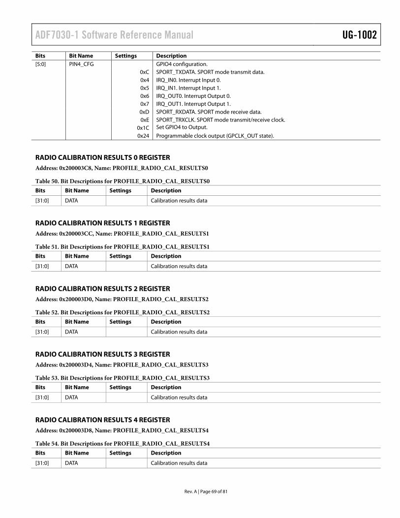
ADF7030-1 Software Reference Manual UG-1002
Rev. A | Page 69 of 81
Bits Bit Name Settings Description [5:0] PIN4_CFG GPIO4 configuration. 0xC SPORT_TXDATA. SPORT mode transmit data. 0x4 IRQ_IN0. Interrupt Input 0. 0x5 IRQ_IN1. Interrupt Input 1. 0x6 IRQ_OUT0. Interrupt Output 0. 0x7 IRQ_OUT1. Interrupt Output 1. 0xD SPORT_RXDATA. SPORT mode receive data. 0xE SPORT_TRXCLK. SPORT mode transmit/receive clock. 0x1C Set GPIO4 to Output. 0x24 Programmable clock output (GPCLK_OUT state).
RADIO CALIBRATION RESULTS 0 REGISTER Address: 0x200003C8, Name: PROFILE_RADIO_CAL_RESULTS0
Table 50. Bit Descriptions for PROFILE_RADIO_CAL_RESULTS0 Bits Bit Name Settings Description
[31:0] DATA Calibration results data
RADIO CALIBRATION RESULTS 1 REGISTER Address: 0x200003CC, Name: PROFILE_RADIO_CAL_RESULTS1
Table 51. Bit Descriptions for PROFILE_RADIO_CAL_RESULTS1 Bits Bit Name Settings Description
[31:0] DATA Calibration results data
RADIO CALIBRATION RESULTS 2 REGISTER Address: 0x200003D0, Name: PROFILE_RADIO_CAL_RESULTS2
Table 52. Bit Descriptions for PROFILE_RADIO_CAL_RESULTS2 Bits Bit Name Settings Description
[31:0] DATA Calibration results data
RADIO CALIBRATION RESULTS 3 REGISTER Address: 0x200003D4, Name: PROFILE_RADIO_CAL_RESULTS3
Table 53. Bit Descriptions for PROFILE_RADIO_CAL_RESULTS3 Bits Bit Name Settings Description
[31:0] DATA Calibration results data
RADIO CALIBRATION RESULTS 4 REGISTER Address: 0x200003D8, Name: PROFILE_RADIO_CAL_RESULTS4
Table 54. Bit Descriptions for PROFILE_RADIO_CAL_RESULTS4 Bits Bit Name Settings Description
[31:0] DATA Calibration results data

UG-1002 ADF7030-1 Software Reference Manual
Rev. A | Page 70 of 81
RADIO CALIBRATION RESULTS 5 REGISTER Address: 0x200003DC, Name: PROFILE_RADIO_CAL_RESULTS5
Table 55. Bit Descriptions for PROFILE_RADIO_CAL_RESULTS5 Bits Bit Name Settings Description
[31:0] DATA Calibration results data
RADIO CALIBRATION RESULTS 6 REGISTER Address: 0x200003E0, Name: PROFILE_RADIO_CAL_RESULTS6
Table 56. Bit Descriptions for PROFILE_RADIO_CAL_RESULTS6 Bits Bit Name Settings Description
[31:0] DATA Calibration results data
RADIO CALIBRATION RESULTS 7 REGISTER Address: 0x200003E4, Name: PROFILE_RADIO_CAL_RESULTS7
Table 57. Bit Descriptions for PROFILE_RADIO_CAL_RESULTS7 Bits Bit Name Settings Description
[31:0] DATA Calibration results data
RADIO CALIBRATION RESULTS 8 REGISTER Address: 0x200003E8, Name: PROFILE_RADIO_CAL_RESULTS8
Table 58. Bit Descriptions for PROFILE_RADIO_CAL_RESULTS8 Bits Bit Name Settings Description
[31:0] DATA Calibration results data
TRANSMIT/RECEIVE BUFFER CONFIGURATION 0 REGISTER Address: 0x200004F4, Name: GENERIC_PKT_BUFF_CFG0
Table 59. Bit Descriptions for GENERIC_PKT_BUFF_CFG0 Bits Bit Name Settings Description
[31:25] GENERATED Generated by the ADF7030-1 design center.
24 ROLLING_BUFF_EN Enable the rolling buffer mode. When the number of bytes received equals RX_SIZE/2 or TX_SIZE/2, the half full IRQ is asserted. When number of bytes received equals RX_SIZE or TX_SIZE, the full IRQ is asserted. When the number of bytes received equals RX_SIZE/2 or TX_SIZE/2, the half full IRQ is asserted. When number of bytes received equals RX_SIZE or TX_SIZE, the full IRQ is asserted.
0 Rolling buffer mode is disabled.
1 Rolling buffer mode is enabled.
23 GENERATED Generated by the ADF7030-1 design center.
22 BIT2AIR For generic packet format Tx: specifies which bit of payload bytes is transmitted first (0 = most significant bit (MSB) first). For generic packet format Rx: specifies into which bit the first bit received of payload is written (0 = MSB).
0 For Tx: MSB of each payload byte is transmitted first. For Rx: first received bit of each payload byte is stored MSB first.
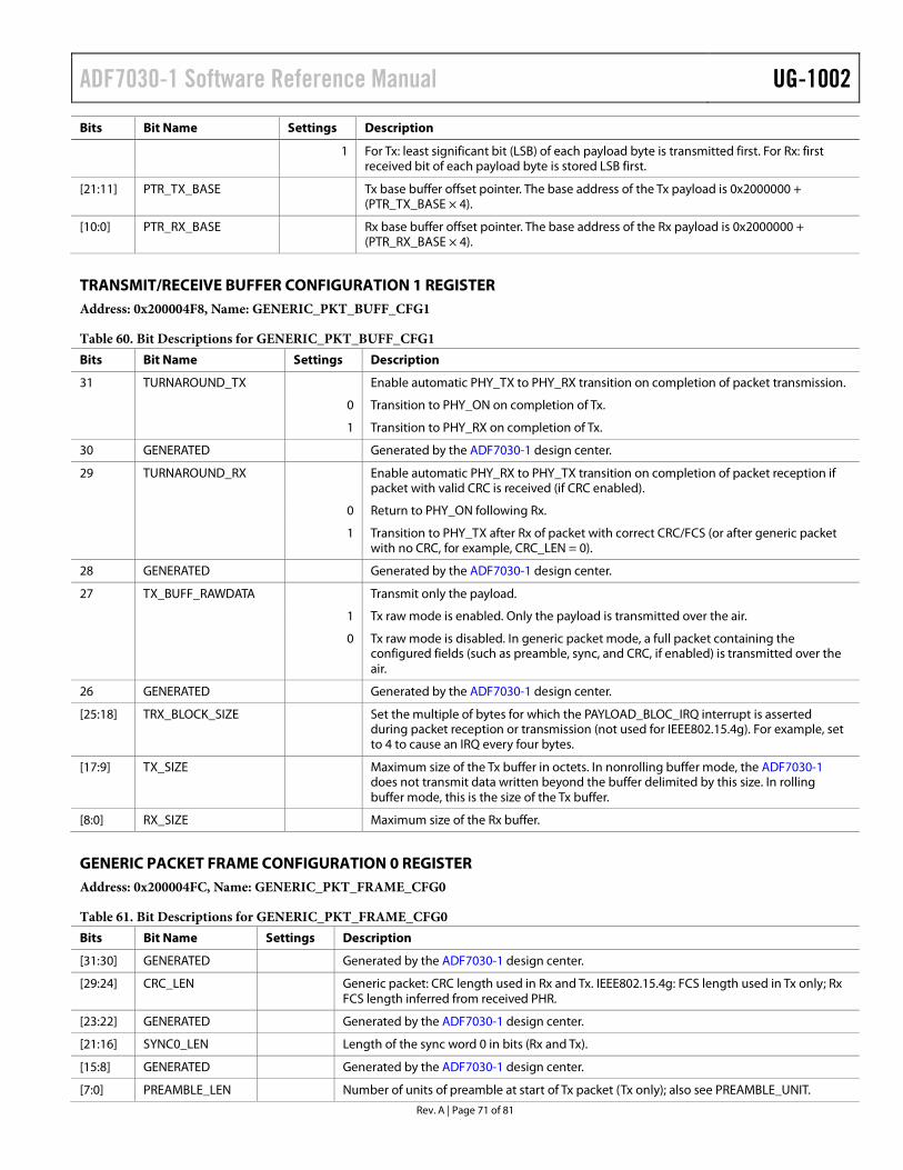
ADF7030-1 Software Reference Manual UG-1002
Rev. A | Page 71 of 81
Bits Bit Name Settings Description
1 For Tx: least significant bit (LSB) of each payload byte is transmitted first. For Rx: first received bit of each payload byte is stored LSB first.
[21:11] PTR_TX_BASE Tx base buffer offset pointer. The base address of the Tx payload is 0x2000000 + (PTR_TX_BASE × 4).
[10:0] PTR_RX_BASE Rx base buffer offset pointer. The base address of the Rx payload is 0x2000000 + (PTR_RX_BASE × 4).
TRANSMIT/RECEIVE BUFFER CONFIGURATION 1 REGISTER Address: 0x200004F8, Name: GENERIC_PKT_BUFF_CFG1
Table 60. Bit Descriptions for GENERIC_PKT_BUFF_CFG1 Bits Bit Name Settings Description
31 TURNAROUND_TX Enable automatic PHY_TX to PHY_RX transition on completion of packet transmission.
0 Transition to PHY_ON on completion of Tx.
1 Transition to PHY_RX on completion of Tx.
30 GENERATED Generated by the ADF7030-1 design center.
29 TURNAROUND_RX Enable automatic PHY_RX to PHY_TX transition on completion of packet reception if packet with valid CRC is received (if CRC enabled).
0 Return to PHY_ON following Rx.
1 Transition to PHY_TX after Rx of packet with correct CRC/FCS (or after generic packet with no CRC, for example, CRC_LEN = 0).
28 GENERATED Generated by the ADF7030-1 design center.
27 TX_BUFF_RAWDATA Transmit only the payload.
1 Tx raw mode is enabled. Only the payload is transmitted over the air.
0 Tx raw mode is disabled. In generic packet mode, a full packet containing the configured fields (such as preamble, sync, and CRC, if enabled) is transmitted over the air.
26 GENERATED Generated by the ADF7030-1 design center.
[25:18] TRX_BLOCK_SIZE Set the multiple of bytes for which the PAYLOAD_BLOC_IRQ interrupt is asserted during packet reception or transmission (not used for IEEE802.15.4g). For example, set to 4 to cause an IRQ every four bytes.
[17:9] TX_SIZE Maximum size of the Tx buffer in octets. In nonrolling buffer mode, the ADF7030-1 does not transmit data written beyond the buffer delimited by this size. In rolling buffer mode, this is the size of the Tx buffer.
[8:0] RX_SIZE Maximum size of the Rx buffer.
GENERIC PACKET FRAME CONFIGURATION 0 REGISTER Address: 0x200004FC, Name: GENERIC_PKT_FRAME_CFG0
Table 61. Bit Descriptions for GENERIC_PKT_FRAME_CFG0 Bits Bit Name Settings Description
[31:30] GENERATED Generated by the ADF7030-1 design center.
[29:24] CRC_LEN Generic packet: CRC length used in Rx and Tx. IEEE802.15.4g: FCS length used in Tx only; Rx FCS length inferred from received PHR.
[23:22] GENERATED Generated by the ADF7030-1 design center.
[21:16] SYNC0_LEN Length of the sync word 0 in bits (Rx and Tx).
[15:8] GENERATED Generated by the ADF7030-1 design center.
[7:0] PREAMBLE_LEN Number of units of preamble at start of Tx packet (Tx only); also see PREAMBLE_UNIT.
UG-1002 ADF7030-1 Software Reference Manual
Rev. A | Page 72 of 81
GENERIC PACKET FRAME CONFIGURATION 1 REGISTER Address: 0x20000500, Name: GENERIC_PKT_FRAME_CFG1
Table 62. Bit Descriptions for GENERIC_PKT_FRAME_CFG1 Bits Bit Name Settings Description
[31:24] TRX_IRQ1_TYPE Select sources of interrupt on IRQ_OUT1 during Rx and Tx.
00000000 Disable all frame IRQs.
00000001 Generic packet and IEEE802.15.4g: preamble has been received (Rx); the first preamble bit is about to be transmitted (Tx).
00000010 Generic packet and IEEE802.15.4g: preamble pattern gone in received bit stream (Rx); last preamble bit transmitted (Tx).
00000100 Generic packet: the programmed number of bits of Sync Word 0 has been received and matched (Rx). IEEE802.15.4g: the programmed number of Sync Word 0 or Sync Word 1 (if enabled) bits has been received and matched (Rx). Generic packet and IEEE802.15.4g: the programmed number of bits of Sync Word 0 have been transmitted (Tx).
00001000 Generic packet: a length field has been received (Rx); the length field has been transmitted (Tx). IEEE802.15.4g: PHR has been received (Rx); the PHR has been transmitted (Tx).
00010000 Generic packet: full payload received (Rx); full payload transmitted (Tx). IEEE802.15.4g: full payload (including FCS) received (Rx); full payload (including FCS) transmitted (Tx).
00100000 Generic packet only: a multiple of TRX_BLOCK_SIZE payload bytes has been received (Rx); a multiple of TRX_BLOCK_SIZE payload bytes have been transmitted (Tx).
01000000 Generic packet and IEEE802.15.4g: the programmed number of CRC/FCS bits has been received and is correct (Rx); the programmed number of CRC/FCS bits has been transmitted (Tx).
10000000 Generic packet and IEEE802.15.4g: the full packet has been received (Rx); the full packet has been transmitted (Tx).
[23:16] TRX_IRQ0_TYPE Select sources of interrupt on IRQ_OUT0 during Rx and Tx.
00000000 Disable all frame IRQs.
00000001 Generic packet and IEEE802.15.4g: preamble has been received (Rx); the first preamble bit is about to be transmitted (Tx).
00000010 Generic packet and IEEE802.15.4g: preamble pattern gone in received bit stream (Rx); last preamble bit transmitted (Tx).
00000100 Generic packet: the programmed number of bits of Sync Word 0 has been received and matched (Rx). IEEE802.15.4g: the programmed number of Sync Word 0 or Sync Word 1 (if enabled) bits has been received and matched (Rx). Generic packet and IEEE802.15.4g: the programmed number of bits of Sync Word 0 has been transmitted (Tx).
00001000 Generic packet: a length field has been received (Rx); the length field has been transmitted (Tx). IEEE802.15.4g: PHR has been received (Rx); the PHR has been transmitted (Tx).
00010000 Generic packet: full payload received (Rx)/Full payload transmitted (Tx). IEEE802.15.4g: full payload (including FCS) received (Rx); full payload (including FCS) transmitted (Tx).
00100000 Generic packet only: a multiple of TRX_BLOCK_SIZE payload bytes has been received (Rx); a multiple of TRX_BLOCK_SIZE payload bytes have been transmitted (Tx).
01000000 Generic packet and IEEE802.15.4g: the programmed number of CRC/FCS bits has been received and is correct (Rx); the programmed number of CRC/FCS bits have been transmitted (Tx).
10000000 Generic packet and IEEE802.15.4g: the full packet has been received (Rx); the full packet has been transmitted (Tx).
[15:13] GENERATED Generated by the ADF7030-1 design center.
12 PREAMBLE_UNIT Unit of preamble length for Tx.
0 PREAMBLE_LEN is in units of bit pairs.
1 PREAMBLE_LEN is in units of octets.

ADF7030-1 Software Reference Manual UG-1002
Rev. A | Page 73 of 81
Bits Bit Name Settings Description
[11:0] PAYLOAD_SIZE Generic packet only: sets number of payload bytes in the Tx packet (raw mode only). In receive mode, PAYLOAD_SIZE sets the number of payload bytes to be received in a fixed length packet, that is, when the LEN_SEL bits in the GENERIC_PKT_FRAME_CFG2 register is set to 0.
GENERIC PACKET FRAME CONFIGURATION 2 REGISTER Address: 0x20000504, Name: GENERIC_PKT_FRAME_CFG2
Table 63. Bit Descriptions for GENERIC_PKT_FRAME_CFG2 Bits Bit Name Settings Description
[31:24] ENDEC_MODE Line coding scheme (generic packet Tx only). The encoding modes are mutually exclusive. The polarity bit can be set independently of the encoding modes.
00000001 Nonreturn to zero (NRZ) encoding.
00000100 Manchester encoding.
00001000 FEC encoding.
10000000 Polarity bit. Set to 1 to invert polarity of the data over the air.
[23:16] PREAMBLE_VAL For Tx, this is the preamble pattern used in the outgoing packet. For Rx, this must be set to the expected preamble, for example, 0x55 or 0xAA. If this field is set to 0, a default value of 0x55 is used.
[15:14] GENERATED Generated by the ADF7030-1 design center.
[13:12] LEN_SEL Selects the size of the length field in the received or transmitted message (Rx and Tx generic packet only).
00 Fixed length mode. There is no length field in the packet.
01 Length field is 8 bits.
10 Length field is 16 bits.
11 CRC_SHIFT_IN_ZEROS Shift in CRC length of zeros after all bytes have passed through CRC calculation. Determines whether the final register value is reversed.
[10:9] GENERATED Generated by the ADF7030-1 design center.
[8:3] SYNC1_LEN Length of the Sync Word 1 in bits. Only used in IEEE802.15.4g Rx.
[2:0] GENERATED Generated by the ADF7030-1 design center.
GENERIC PACKET FRAME CONFIGURATION 3 REGISTER Address: 0x20000508, Name: GENERIC_PKT_FRAME_CFG3
Table 64. Bit Descriptions for GENERIC_PKT_FRAME_CFG3 Bits Bit Name Settings Description
[31:16] RX_LENGTH Generic packet Rx: the contents of the length field in the received packet. IEEE802.15.4g: the received PHR.
[15:0] GENERATED Generated by the ADF7030-1 design center.
GENERIC PACKET FRAME CONFIGURATION 5 REGISTER Address: 0x20000510, Name: GENERIC_PKT_FRAME_CFG5
Table 65. Bit Descriptions for GENERIC_PKT_FRAME_CFG5 Bits Bit Name Settings Description
[31:16] GENERATED Generated by the ADF7030-1 design center.
[15:0] TX_PHR PHY header (PHR) used as first two octets of IEEE802.15.4g Tx packet.

UG-1002 ADF7030-1 Software Reference Manual
Rev. A | Page 74 of 81
SYNC WORD 0 REGISTER Address: 0x20000514, Name: GENERIC_PKT_SYNCWORD0
Table 66. Bit Descriptions for GENERIC_PKT_SYNCWORD0 Bits Bit Name Settings Description
[31:0] VAL Generic packet: sync word used in Rx and Tx. IEEE802.15.4g: SFD for FEC encoded packets (Rx and Tx)
SYNC WORD 1 REGISTER Address: 0x20000518, Name: GENERIC_PKT_SYNCWORD1
Table 67. Bit Descriptions for GENERIC_PKT_SYNCWORD1 Bits Bit Name Settings Description
[31:0] VAL IEEE802.15.4g: SFD for nonFEC encoded packets (Rx and Tx)
CRC POLYNOMIAL REGISTER Address: 0x2000051C, Name: GENERIC_PKT_CRC_POLY
Table 68. Bit Descriptions for GENERIC_PKT_CRC_POLY Bits Bit Name Settings Description
[31:0] VAL Generic packet: CRC polynomial used in Rx and Tx. IEEE802.15.4g: FCS polynomial used in Tx only (in Rx, the FCS polynomial is inferred from the received PHR; this field is unused in that case).
CRC INITIAL SEED REGISTER Address: 0x20000520, Name: GENERIC_PKT_CRC_SEED
Table 69. Bit Descriptions for GENERIC_PKT_CRC_SEED Bits Bit Name Settings Description
[31:0] VAL Generic Packet: CRC seed used in Rx and Tx. IEEE802.15.4g: FCS seed used in Tx only (in Rx, the FCS seed is inferred from the received PHR; this field is unused in that case).
CRC XOR VALUE REGISTER Address: 0x20000524, Name: GENERIC_PKT_CRC_FINAL_XOR
Table 70. Bit Descriptions for GENERIC_PKT_CRC_FINAL_XOR Bits Bit Name Settings Description
[31:0] VAL Value to be XOR'd with the final value CRC. If the result is 0, the received packet CRC is valid.
ADF7030-1 Software Reference Manual UG-1002
Rev. A | Page 75 of 81
RSSI CONFIGURATION REGISTER Address: 0x2000052C, Name: GENERIC_PKT_TICK_CFG
Table 71. Bit Descriptions for GENERIC_PKT_TICK_CFG Bits Bit Name Settings Description
[31:8] GENERATED Generated by the ADF7030-1 design center.
[7:4] SEARCH_POSTSCALAR Adjusts the CCA tick time.
[3:0] SEARCH_RATE Sets the CCA tick time.
0x1 Tx user clock (phase adjusted from CDR clock).
0x2 2× data rate.
0x3 4× data rate.
0x4 8× data rate.
0x5 16× data rate.
0x6 32× data rate.
0x7 32× data rate.
0x8 32× data rate.
RX LINK QUALITY READBACK REGISTER Address: 0x20000538, Name: GENERIC_PKT_LIVE_LINK_QUAL
Table 72. Bit Descriptions for GENERIC_PKT_LIVE_LINK_QUAL Bits Bit Name Settings Description
[31:27] RESERVED Bits set to 0.
[26:16] RSSI RSSI as a signed 11-bit value in units of 0.25 dBm measured during packet reception.
[15:0] GENERATED Generated by the ADF7030-1 design center.
LOW POWER MODE CONFIGURATION REGISTER Address: 0x20000544, Name: GENERIC_PKT_LPM_CFG
Table 73. Bit Descriptions for GENERIC_PKT_LPM_CFG Bits Bit Name Settings Description
[31:24] PREAMBLE_DETECT_DWELL_TIME Number of symbols allowed for preamble detection.
[23:16] PREAMBLE_QUAL_DWELL_TIME Number of symbols allowed for preamble qualification.
[15:8] PREAMBLE_DWELL_TIME Generated by the ADF7030-1 design center.
[7:0] GENERATED Generated by the ADF7030-1 design center.

UG-1002 ADF7030-1 Software Reference Manual
Rev. A | Page 76 of 81
TEST MODE CONFIGURATION 0 REGISTER Address: 0x20000548, Name: GENERIC_PKT_TEST_MODES0
Table 74. Bit Descriptions for GENERIC_PKT_TEST_MODES0 Bits Bit Name Settings Description
[31:20] GENERATED Generated by the ADF7030-1 design center.
[19:16] TX_TEST Continuous Tx test modes
000 Test modes disabled.
001 Transmit a carrier.
010 Transmit −fDEV in 2FSK or off in OOK.
011 Transmit −fDEV_MAX in 4FSK only.
100 Transmit +fDEV in 2FSK or on in OOK.
101 Transmit + fDEV_MAX in 4FSK only.
110 Transmit preamble pattern.
111 Transmit pseudorandom (PN9) sequence.
1000 Transmit custom pseudorandom (PN) sequence.
[15:0] GENERATED Generated by the ADF7030-1 design center.
GATEWAY FOR SOFTWARE KEYED INSTRUCTIONS REGISTER Address: 0x40000C08, Name: PMU_KEY
Table 75. Bit Descriptions for PMU_KEY Bits Bit Name Settings Description
[31:6] GENERATED Generated by the ADF7030-1 design center.
[5:0] SW_KEY Software keyed instruction to the PMU. Software key.
PMU CLOCK CONTROL REGISTER Address: 0x40000C20, Name: PMU_CLOCKS
Table 76. Bit Descriptions for PMU_CLOCKS Bits Bit Name Settings Description [31:1] RESERVED Reserved.
0 HFRC_PD_N High frequency RC oscillator reset, active low.
0 Power down the high frequency RC oscillator.
1 Do not power down the high frequency RC oscillator.
SPI SLAVE POINTER 0 REGISTER Address: 0x40001800, Name: SPI_HOST_PNTR0
Table 77. Bit Descriptions for SPI_HOST_PNTR0 Bits Bit Name Settings Description [31:0] SPIS_PNTR0 SPI Pointer 0. This register contains the target address within the memory system of any memory reads
or writes that use a pointer-based protocol with SPIS_PNTR0 selected as the pointer.

ADF7030-1 Software Reference Manual UG-1002
Rev. A | Page 77 of 81
SPI SLAVE POINTER 1 REGISTER Address: 0x40001804, Name: SPI_HOST_PNTR1
Table 78. Bit Descriptions for SPI_HOST_PNTR1 Bits Bit Name Settings Description [31:0] SPIS_PNTR1 SPI Pointer 1. This register contains the target address within the memory system of any memory reads
or writes that use a pointer-based protocol with SPIS_PNTR1 selected as the pointer.
SPI SLAVE POINTER 2 REGISTER Address: 0x40001808, Name: SPI_HOST_PNTR2
Table 79. Bit Descriptions for SPI_HOST_PNTR2 Bits Bit Name Settings Description [31:0] SPIS_PNTR2 SPI Pointer 2. This register contains the target address within the memory system of any memory reads
or writes that use a pointer-based protocol with SPIS_PNTR2 selected as the pointer.
MASK FOR EXTERNAL INTERRUPT 0 (IRQ_OUT0) REGISTER Address: 0x40003800, Name: IRQ_CTRL_MASK0
When a bit is cleared, the corresponding interrupt source for IRQ0 is disabled; when set, it is enabled.
Table 80. Bit Descriptions for IRQ_CTRL_MASK0 Bits Bit Name Settings Description
[31:12] GENERATED Generated by the ADF7030-1 design center.
11 SM_IDLE_IRQ0 SM_IDLE event has occurred. The destination state has been reached and all actions associated with the destination state have been completed. The complete state transition is complete (write 1 to clear).
10 SM_READY_IRQ0 SM_RDY event has occurred. The last state transition command has been received and the transition from the origin state to destination state is underway. A new command can be issued at this point to interrupt the current transition. It indicates that CMD_READY is 1 (write 1 to clear).
9 BUFF_FULL_IRQ0 Rx: the upper half of Rx rolling buffer is full. Tx: the upper half of Tx rolling buffer is empty (write 1 to clear event).
8 BUFF_HALF_IRQ0 Rx: the lower half of Rx rolling buffer is full. Tx: the lower half of Tx rolling buffer is empty (write 1 to clear event).
[7:0] GENERATED Generated by the ADF7030-1 design center.
MASK FOR EXTERNAL INTERRUPT 1 (IRQ_OUT1) REGISTER Address: 0x40003804, Name: IRQ_CTRL_MASK1
When a bit is cleared, the corresponding interrupt source for IRQ n is disabled; when set, it is enabled.
Table 81. Bit Descriptions for IRQ_CTRL_MASK1 Bits Bit Name Settings Description
[31:12] GENERATED Generated by the ADF7030-1 design center.
11 SM_IDLE_IRQ1 SM_IDLE event has occurred. The destination state has been reached and all actions associated with the destination state have been completed. The complete state transition is complete (write 1 to clear).
10 SM_READY_IRQ1 SM_RDY event has occurred. The last state transition command has been received and the transition from the origin state to destination state is underway. A new command can be issued at this point to interrupt the current transition. It indicates that CMD_READY is 1 (write 1 to clear).

UG-1002 ADF7030-1 Software Reference Manual
Rev. A | Page 78 of 81
Bits Bit Name Settings Description
9 BUFF_FULL_IRQ1 Rx: the upper half of Rx rolling buffer is full. Tx: the upper half of the Tx rolling buffer is empty (write 1 to clear event).
8 BUFF_HALF_IRQ1 Rx: the lower half of Rx rolling buffer is full. Tx: the lower half of the Tx rolling buffer is empty (write 1 to clear event).
[7:0] GENERATED Generated by the ADF7030-1 design center.
EXTERNAL INTERRUPT 0 (IRQ_OUT0) STATUS REGISTER Address: 0x40003808, Name: IRQ_CTRL_STATUS0
Table 82. Bit Descriptions for IRQ_CTRL_STATUS0 Bits Bit Name Settings Description
[31:12] GENERATED Generated by the ADF7030-1 design center.
11 SM_IDLE_IRQ0 SM_IDLE event has occurred. The destination state has been reached and all actions associated with the destination state have been completed. Write 1 to clear.
10 SM_READY_IRQ0 SM_RDY event has occurred. The last state transition command has been received and the transition from the origin state to destination state is underway. A new command can be issued at this point to interrupt the current transition. It indicates that CMD_READY is 1; write 1 to clear.
9 BUFF_FULL_IRQ0 RX: the upper half of Rx rolling buffer is full. Tx: the upper half of Tx rolling buffer is empty (write 1 to clear event).
8 BUFF_HALF_IRQ0 RX: the lower half of Rx rolling buffer is full. Tx: the lower half of Tx rolling buffer is empty (write 1 to clear).
7 EOF_IRQ0 Generic packet and IEEE802.15.4g: the full packet has been received (Rx); the full packet has been transmitted (Tx).
6 CRC_CHK_IRQ0 Generic packet and IEEE802.15.4g: the programmed number of CRC/FCS bits has been received and is correct (Rx); the programmed number of CRC/FCS bits has been transmitted (Tx).
5 PAYLOAD_BLOC_IRQ0 Generic packet only: a multiple of TRX_BLOCK_SIZE payload bytes has been received (Rx); a multiple of TRX_BLOCK_SIZE payload bytes has been transmitted (Tx).
4 PAYLOAD_IRQ0 Generic packet: full payload received (Rx)/full payload transmitted (Tx). IEEE802.15.4g: full payload (including FCS) received (Rx); full payload (including FCS) transmitted (Tx).
3 LENGTH_IRQ0 Generic packet: a length field has been received (Rx); the length field has been transmitted (Tx). IEEE802.15.4g: PHR has been received (Rx); the PHR has been transmitted (Tx).
2 SYNCWORD_IRQ0 Generic packet: the programmed number of bits of Sync Word 0 has been received and matched (Rx). IEEE802.15.4g: the programmed number of Sync Word 0 or Sync Word 1 (if enabled) bits has been received and matched (Rx). Generic packet and IEEE802.15.4g: the programmed number of bits of Sync Word 0 has been transmitted (Tx).
1 PREAMBLE_GONE_IRQ0 Generic packet and IEEE802.15.4g: preamble pattern is no longer being received in received bit stream (Rx); last preamble bit transmitted (Tx).
0 PREAMBLE_IRQ0 Generic packet and IEEE802.15.4g: preamble has been received (Rx); the first preamble bit is about to be transmitted (Tx).
ADF7030-1 Software Reference Manual UG-1002
Rev. A | Page 79 of 81
EXTERNAL INTERRUPT 1 (IRQ_OUT1) STATUS REGISTER Address: 0x4000380C, Name: IRQ_CTRL_STATUS1
Table 83. Bit Descriptions for IRQ_CTRL_STATUS1 Bits Bit Name Settings Description
[31:12] GENERATED Generated by the ADF7030-1 design center.
11 SM_IDLE_IRQ1 SM_IDLE event has occurred. The destination state has been reached and all actions associated with the destination state have been completed. Write 1 to clear.
10 SM_READY_IRQ1 SM_RDY event has occurred. The last state transition command has been received and the transition from the origin state to destination state is underway. A new command can be issued at this point to interrupt the current transition. It indicates that CMD_READY is 1; write 1 to clear.
9 BUFF_FULL_IRQ1 Rx: the upper half of Rx rolling buffer is full. Tx: the upper half of Tx rolling buffer is empty (write 1 to clear event).
8 BUFF_HALF_IRQ1 Rx: the lower half of Rx rolling buffer is full. Tx: the lower half of Tx rolling buffer is empty (write 1 to clear).
7 EOF_IRQ1 Generic packet and IEEE802.15.4g: the full packet has been received (Rx); the full packet has been transmitted (Tx).
6 CRC_CHK_IRQ1 Generic packet and IEEE802.15.4g: the programmed number of CRC/FCS bits has been received and are correct (Rx); the programmed number of CRC/FCS bits has been transmitted (Tx).
5 PAYLOAD_BLOC_IRQ1 Generic packet only: a multiple of TRX_BLOCK_SIZE payload bytes has been received (Rx); a multiple of TRX_BLOCK_SIZE payload bytes has been transmitted (Tx).
4 PAYLOAD_IRQ1 Generic packet: full payload received (Rx); full payload transmitted (Tx). IEEE802.15.4g: full payload (including FCS) received (Rx); full payload (including FCS) transmitted (Tx).
3 LENGTH_IRQ1 Generic packet: a length field has been received (Rx); the length field has been transmitted (Tx). IEEE802.15.4g: PHR has been received (Rx); the PHR has been transmitted (Tx).
2 SYNCWORD_IRQ1 Generic packet: the programmed number of bits of Sync word 0 has been received and matched (Rx). IEEE802.15.4g: the programmed number of Sync Word 0 or Sync Word 1 (if enabled) bits has been received and matched (Rx). Generic packet and IEEE802.15.4g: the programmed number of bits of Sync Word 0 has been transmitted (Tx).
1 PREAMBLE_GONE_IRQ1 Generic packet and IEEE802.15.4g: preamble pattern is no longer being received in received bit stream (Rx); last preamble bit transmitted (Tx).
0 PREAMBLE_IRQ1 Generic packet and IEEE802.15.4g: preamble has been received (Rx); the first preamble bit is about to be transmitted (Tx).
AFC CONFIGRATION REGISTER Address: 0x400041F8, Name: AFC_CONFIG
Table 84. Bit Descriptions for AFC_CONFIG Bits Bit Name Settings Description [31:3] GENERATED Generated by the ADF7030-1 design center. [2:0] MODE Set AFC mode. 0 Disable AFC.

UG-1002 ADF7030-1 Software Reference Manual
Rev. A | Page 80 of 81
AFC FREQUENCY ERROR READBACK REGISTER Address: 0x40004208, Name: AFC_FREQUENCY_ERROR
Table 85. Bit Descriptions for AFC_FREQUENCY_ERROR Bits Bit Name Settings Description
[31:16] GENERATED Generated by the ADF7030-1 design center.
[15:0] READBACK Frequency error correction signed 16-bit readback value. Frequency error in Hz = readback × 26,000,000/222.
PROCESSOR CLOCK ENABLE REGISTER Address: 0x40004278, Name: CRMGT_PROC_CLK_EN
Table 86. Bit Descriptions for CRMGT_PROC_CLK_EN Bits Bit Name Settings Description
[31:0] CONFIGURATION Processor clock configuration
FIRMWARE STATUS AND DEBUG REGISTER Address: 0x400042B4, Name: MISC_FW
Table 87. Bit Descriptions for MISC_FW Bits Bit Name Settings Description
[31:14] GENERATED Generated by the ADF7030-1 design center.
[13:8] CURR_STATE Current firmware state readback.
00000 PHY_SLEEP.
00001 PHY_OFF.
00010 PHY_ON.
00011 PHY_RX.
00100 PHY_TX.
00101 Configuring.
00110 CCA.
01001 Calibrating.
01010 Monitoring.
[7:2] GENERATED Generated by the ADF7030-1 design center.
[1:0] STATUS Firmware status ID.
00 ADF7030-1 is in transition between radio states.
01 ADF7030-1 is executing a state function (that is, active).
10 ADF7030-1 has completed a state transition and is idle (that is, no longer executing a state function).

ADF7030-1 Software Reference Manual UG-1002
Rev. A | Page 81 of 81
NOTES
Legal Terms and Conditions
Information furnished by Analog Devices is believed to be accurate and reliable. However, no responsibility is assumed by Analog Devices for its use, nor for any infringements of patents or other rights of third parties that may result from its use. No license is granted by implication or otherwise under any patent or patent rights of Analog Devices. Trademarks and registered trademarks are the property of their respective owners. Information contained within this document is subject to change without notice. Software or hardware provided by Analog Devices may not be disassembled, decompiled or reverse engineered. Analog Devices’ standard terms and conditions for products purchased from Analog Devices can be found at: http://www.analog.com/en/content/analog_devices_terms_and_conditions/fca.html.
©2017 Analog Devices, Inc. All rights reserved. Trademarks and registered trademarks are the property of their respective owners. UG14686-0-1/17(A)