Design of Power-Rail ESD Clamp Circuit with Adjustable Holding

536 IEEE TRANSACTIONS ON DEVICE AND MATERIALS RELIABILITY, VOL. 14, NO. 1, MARCH 2014
On the Design of Power-Rail ESD Clamp CircuitsWith Gate Leakage Consideration in
Nanoscale CMOS TechnologyMing-Dou Ker, Fellow, IEEE, and Chih-Ting Yeh, Member, IEEE
Abstract—CMOS technology has been widely used to producemany integrated circuits. However, the thinner gate oxide innanoscale CMOS technology seriously increases the difficulty ofelectrostatic discharge (ESD) protection design. The power-railESD clamp circuit has been the key circuit to perform thewhole-chip ESD protection scheme. Some ESD detection circuitswere developed to trigger on ESD devices across the power railsto quickly discharge ESD current away from the internal cir-cuits. Therefore, on-chip ESD protection circuits must be designedwith the consideration of standby leakage to minimize the powerconsumption and the possibility of malfunction to normal circuitoperation. The design of power-rail ESD clamp circuits withlow standby leakage current and high efficiency of layout areain nanoscale CMOS technology is reviewed in this paper. Thecomparisons among those power-rail ESD clamp circuits are alsodiscussed.
Index Terms—Electrostatic discharge (ESD), gate leakage, lay-out area, power-rail ESD clamp circuit.
I. INTRODUCTION
E LECTROSTATIC discharge (ESD) phenomenon is acharge flow when two objects with different voltage po-
tentials reach contact. ESD is the result of the charge balancebetween the two objects in a very short period of time. Such anESD event can damage the integrated circuits (ICs). In order toprotect the IC products with the required ESD specifications,such as 2 kV in human-body-model (HBM) [1] and 200 V inmachine-model [2], whole-chip ESD protection scheme formedwith the power-rail ESD clamp circuit had been widely used[3]. As shown in Fig. 1, the power-rail ESD clamp circuit isa vital element for ESD protection under different ESD stressmodes. The ESD stress modes include VDD-to-VSS (or VSS-to-VDD) ESD stress between the rails; as well as the positive-to-VSS (PS) mode, negative-to-VSS mode, positive-to-VDD
Manuscript received July 7, 2013; revised August 20, 2013; acceptedAugust 25, 2013. Date of publication August 29, 2013; date of current versionMarch 4, 2014. This work was supported in part by the National ScienceCouncil (NSC), Taiwan, under Contracts NSC 102-2220-E-009-004 and NSC101-113-P-110-004.
M.-D. Ker is with the Department of Electronics Engineering and Insti-tute of Electronics, National Chiao Tung University, Hsinchu 300, Taiwan(e-mail: [email protected]).
C.-T. Yeh is with the Institute of Electronics, National Chiao Tung Univer-sity, Hsinchu 300, Taiwan, and also with the Information and CommunicationsResearch Laboratories, Industrial Technology Research Institute, Hsinchu 310,Taiwan.
Color versions of one or more of the figures in this paper are available onlineat http://ieeexplore.ieee.org.
Digital Object Identifier 10.1109/TDMR.2013.2280044
Fig. 1. Typical whole-chip ESD protection scheme with the power-rail ESDclamp circuit under different ESD stress conditions.
mode, and negative-to-VDD mode, from input/output (I/O) toVDD/VSS. Therefore, the power-rail ESD clamp circuit mustprovide low-impedance discharging path under ESD eventsbut keep in OFF state with standby leakage current as low aspossible under normal circuit operation conditions.
In advanced nanoscale CMOS technology, there are twocommonly used processes provided from foundry for specificpurpose. They are low-power (LP) and general-purpose (GP)processes. LP process is used for low-power product with a1.2-V core design and 2.5- or 3.3-V I/O option. Because LP pro-cess is developed for low-power product, there is basically noserious gate leakage issue. Therefore, a large-sized MOSFETdrawn in the layout style of big field-effect transistor (BigFET)is usually adopted as the ESD clamp device in the power-railESD clamp circuit.
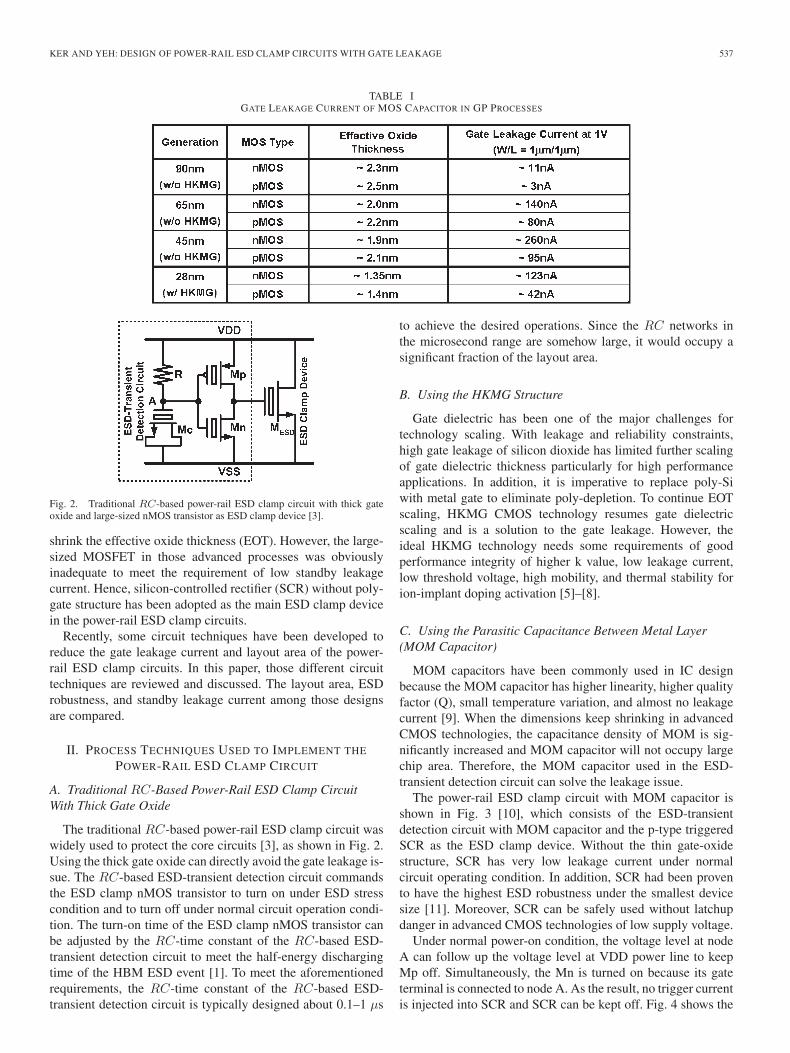
GP process provides higher performance transistors for high-speed or high-frequency applications with 1-V core design and2.5-V I/O option. In GP process, the thickness of gate oxidelayer is thinner than that in LP process (or with a lower thresh-old voltage, i.e., Vth) to gain higher driving current. However,the thinner gate oxide seriously impacts on the ESD protectioncircuits due to the intolerable gate leakage and the lower break-down voltage. A comparison of gate leakage issue on MOScapacitor (W/L = 1 μm/1 μm) among different CMOS tech-nologies is shown in Table I. In the 28-nm technology node, thestructure of high-k/metal gate (HKMG) [4] has been adoptedto reduce the gate leakage current issue and to continuously
1530-4388 © 2013 IEEE. Personal use is permitted, but republication/redistribution requires IEEE permission.See http://www.ieee.org/publications_standards/publications/rights/index.html for more information.
KER AND YEH: DESIGN OF POWER-RAIL ESD CLAMP CIRCUITS WITH GATE LEAKAGE 537
TABLE IGATE LEAKAGE CURRENT OF MOS CAPACITOR IN GP PROCESSES
Fig. 2. Traditional RC-based power-rail ESD clamp circuit with thick gateoxide and large-sized nMOS transistor as ESD clamp device [3].
shrink the effective oxide thickness (EOT). However, the large-sized MOSFET in those advanced processes was obviouslyinadequate to meet the requirement of low standby leakagecurrent. Hence, silicon-controlled rectifier (SCR) without poly-gate structure has been adopted as the main ESD clamp devicein the power-rail ESD clamp circuits.
Recently, some circuit techniques have been developed toreduce the gate leakage current and layout area of the power-rail ESD clamp circuits. In this paper, those different circuittechniques are reviewed and discussed. The layout area, ESDrobustness, and standby leakage current among those designsare compared.
II. PROCESS TECHNIQUES USED TO IMPLEMENT THE
POWER-RAIL ESD CLAMP CIRCUIT
A. Traditional RC-Based Power-Rail ESD Clamp CircuitWith Thick Gate Oxide
The traditional RC-based power-rail ESD clamp circuit waswidely used to protect the core circuits [3], as shown in Fig. 2.Using the thick gate oxide can directly avoid the gate leakage is-sue. The RC-based ESD-transient detection circuit commandsthe ESD clamp nMOS transistor to turn on under ESD stresscondition and to turn off under normal circuit operation condi-tion. The turn-on time of the ESD clamp nMOS transistor canbe adjusted by the RC-time constant of the RC-based ESD-transient detection circuit to meet the half-energy dischargingtime of the HBM ESD event [1]. To meet the aforementionedrequirements, the RC-time constant of the RC-based ESD-transient detection circuit is typically designed about 0.1–1 μs
to achieve the desired operations. Since the RC networks inthe microsecond range are somehow large, it would occupy asignificant fraction of the layout area.
B. Using the HKMG Structure
Gate dielectric has been one of the major challenges fortechnology scaling. With leakage and reliability constraints,high gate leakage of silicon dioxide has limited further scalingof gate dielectric thickness particularly for high performanceapplications. In addition, it is imperative to replace poly-Siwith metal gate to eliminate poly-depletion. To continue EOTscaling, HKMG CMOS technology resumes gate dielectricscaling and is a solution to the gate leakage. However, theideal HKMG technology needs some requirements of goodperformance integrity of higher k value, low leakage current,low threshold voltage, high mobility, and thermal stability forion-implant doping activation [5]–[8].
C. Using the Parasitic Capacitance Between Metal Layer(MOM Capacitor)
MOM capacitors have been commonly used in IC designbecause the MOM capacitor has higher linearity, higher qualityfactor (Q), small temperature variation, and almost no leakagecurrent [9]. When the dimensions keep shrinking in advancedCMOS technologies, the capacitance density of MOM is sig-nificantly increased and MOM capacitor will not occupy largechip area. Therefore, the MOM capacitor used in the ESD-transient detection circuit can solve the leakage issue.
The power-rail ESD clamp circuit with MOM capacitor isshown in Fig. 3 [10], which consists of the ESD-transientdetection circuit with MOM capacitor and the p-type triggeredSCR as the ESD clamp device. Without the thin gate-oxidestructure, SCR has very low leakage current under normalcircuit operating condition. In addition, SCR had been provento have the highest ESD robustness under the smallest devicesize [11]. Moreover, SCR can be safely used without latchupdanger in advanced CMOS technologies of low supply voltage.
Under normal power-on condition, the voltage level at nodeA can follow up the voltage level at VDD power line to keepMp off. Simultaneously, the Mn is turned on because its gateterminal is connected to node A. As the result, no trigger currentis injected into SCR and SCR can be kept off. Fig. 4 shows the
538 IEEE TRANSACTIONS ON DEVICE AND MATERIALS RELIABILITY, VOL. 14, NO. 1, MARCH 2014
Fig. 3. Power-rail ESD clamp circuit with MOM capacitor [10].
Fig. 4. Simulated transient waveforms of the ESD-transient detection circuitwith MOM capacitor under normal power-on transition.
simulated transient waveforms with a rise time of 0.1 ms. Withthe power supply voltage of 1 V, the simulated overall leakagecurrent of the power-rail ESD clamp circuit is only about307 nA at 25 ◦C.
III. CIRCUIT TECHNIQUES USED TO IMPLEMENT THE
POWER-RAIL ESD CLAMP CIRCUIT
A. Feedback-Enhanced Triggering Technique
The power-rail ESD clamp circuit with feedback-enhancedtriggering was depicted in Fig. 5 [12]. A fast positive-goingvoltage pulse on the VDD power rail causes node A to instan-taneously rise along with the VDD potential. The elevation ofnode A causes MESD to be turned on and ESD current can bedischarged. Once the potential of node C has been raised to thevoltage level above the threshold voltage of Mnf, Mnf beginsto conduct. Current conduction in transistor Mnf further pullsthe potential of node B toward ground, which further enhancescurrent conduction in transistor Mp2, which then pulls thepotential of node C closer to that of the VDD power line. Thiscompletes a feedback loop to latch MESD into a conductivestate.
Once MESD has been latched into a conductive state, thetime constant of the RC circuit is now free to time out. Theduration of this time constant can be significantly shorter thanthe ESD event, which translates into an RC network withgreatly reduced physical area. However, the transistors of thefeedback loop and the ESD clamp device in this design needsome modifications to reduce the gate leakage.
Fig. 5. Power-rail ESD clamp circuit with feedback-enhanced triggering andESD clamp nMOS transistor [12].
Fig. 6. Power-rail ESD clamp circuit with cascaded pMOS feedback tech-nique and ESD clamp nMOS transistor [13].
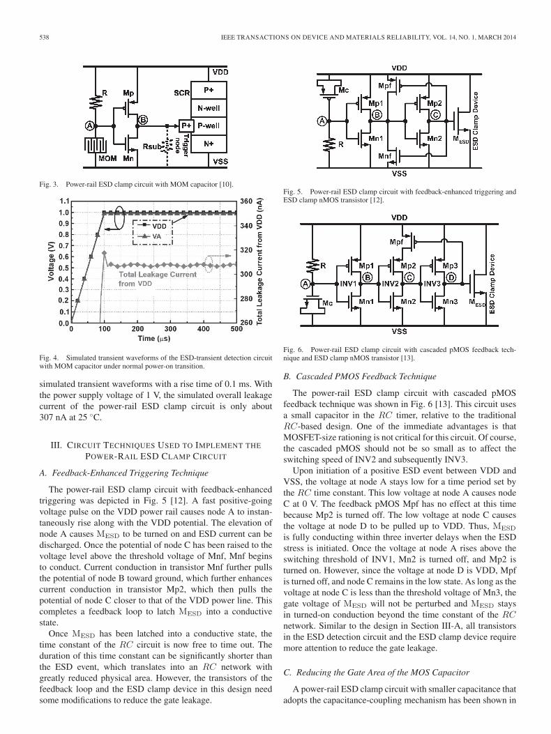
B. Cascaded PMOS Feedback Technique
The power-rail ESD clamp circuit with cascaded pMOSfeedback technique was shown in Fig. 6 [13]. This circuit usesa small capacitor in the RC timer, relative to the traditionalRC-based design. One of the immediate advantages is thatMOSFET-size rationing is not critical for this circuit. Of course,the cascaded pMOS should not be so small as to affect theswitching speed of INV2 and subsequently INV3.
Upon initiation of a positive ESD event between VDD andVSS, the voltage at node A stays low for a time period set bythe RC time constant. This low voltage at node A causes nodeC at 0 V. The feedback pMOS Mpf has no effect at this timebecause Mp2 is turned off. The low voltage at node C causesthe voltage at node D to be pulled up to VDD. Thus, MESD
is fully conducting within three inverter delays when the ESDstress is initiated. Once the voltage at node A rises above theswitching threshold of INV1, Mn2 is turned off, and Mp2 isturned on. However, since the voltage at node D is VDD, Mpfis turned off, and node C remains in the low state. As long as thevoltage at node C is less than the threshold voltage of Mn3, thegate voltage of MESD will not be perturbed and MESD staysin turned-on conduction beyond the time constant of the RCnetwork. Similar to the design in Section III-A, all transistorsin the ESD detection circuit and the ESD clamp device requiremore attention to reduce the gate leakage.
C. Reducing the Gate Area of the MOS Capacitor
A power-rail ESD clamp circuit with smaller capacitance thatadopts the capacitance-coupling mechanism has been shown in

KER AND YEH: DESIGN OF POWER-RAIL ESD CLAMP CIRCUITS WITH GATE LEAKAGE 539
Fig. 7. Power-rail ESD clamp circuit with smaller capacitance in ESD-transient detection circuit [14].
Fig. 8. Power-rail ESD clamp circuit with feedback-control inverter [16].
Fig. 7 [14]. The cascade nMOS transistors (Mnc1 and Mnc2)operated in the saturation region are used as a large resistor andcombined with the smaller capacitor to construct a capacitance-coupling network. Under ESD stress condition, the potentialof node A will be synchronously elevated toward a positivevoltage potential by capacitance coupling of the smaller capac-itor. Then, the gate terminal of the ESD clamp nMOS transistorwill be promptly charged toward the positive voltage potential.Under normal circuit operation condition, the potential of nodeA will actually be kept at VSS through the high resistance pathof the cascade nMOS transistors. Therefore, the ESD clampnMOS transistor will be kept at the OFF state under normalcircuit operation condition. For reducing the total standbyleakage current of this design in nanoscale CMOS technology,the device sizes of inverter can be shrunk, and the ESD clampdevice can be replaced by SCR.
D. Reducing the Voltage Drop Across the MOS Capacitor (I)
The equations of the gate-direct-tunneling current fromBSIM4 MOSFET model [15] indicate that the leakage currentthrough the MOS capacitor can be reduced by reducing thevoltage across it. Based on this concept, the power-rail ESDclamp circuit with feedback-control inverter to overcome thegate leakage issue is shown in Fig. 8 [16]. In the ESD-transientdetection circuit, the RC-based ESD-transient detection circuitand the feedback-control inverter are combined together, andthe MOS capacitor Mcap is connected between nodes A andB. Because Mcap is not directly connected to VSS, no directleakage path is conducted through Mcap to the ground under
Fig. 9. Simulated transient waveforms on the node voltages in the ESD-transient detection circuit with feedback-control inverter under normal power-on transition.
normal circuit operating condition. Without the thin gate oxide,the SCR used as the main ESD clamp device is also free to thegate leakage issue as compared with a large-sized MOSFET.
With a slow rise time of the normal power-on transition,the voltage level at node A will be able to follow up thevoltage level at VDD power line to keep Mp1 off. The parasiticp-substrate resistor Rsub in SCR can pull node C to VSS.Mp3 would be also turned on to drive node B to VDD. Withthe voltage of VDD at node B, Mp2 can be fully turned off.In addition, Mn1 is turned on because its gate terminal isconnected to node B. Obviously, there is no voltage drop acrossMcap, and no circuit leakage path exists in the ESD-transientdetection circuit. Without a voltage drop across Mcap undernormal circuit operating condition, Mcap can be realized witha large device size without suffering the leakage current. Sincenodes A and B are charged to VDD, Mp1 and Mp2 can be fullyturned off during the normal power-on transition. Therefore, notrigger current is injected into the SCR, and the SCR can bekept off under normal circuit operating condition.
Fig. 9 shows the simulated transient waveforms of the ESD-transient detection circuit under the normal power-on transitionwith a rise time of 0.1 ms. With the power supply voltage of1 V, the overall simulated leakage current of the ESD-transientdetection circuit is only about 104 nA at 25 ◦C.
E. Reducing the Voltage Drop Across the MOS Capacitor (II)
The power-rail ESD clamp circuit with the consideration ofthe gate current is shown in Fig. 10 [17]. The SCR device isused as the main ESD clamp device. Utilizing the gate currentto bias the ESD-transient detection circuit and to reduce thevoltage difference across the gates of the MOS capacitors,the gate leakage current through the MOS capacitor underthe normal circuit operating condition can be further reduced.Therefore, the total leakage current resulted from the MOScapacitor in the ESD-transient detection circuit can be wellcontrolled and minimized.
In the ESD-transient detection circuit, Mp1 is used to gener-ate the triggering current into the trigger node of the SCR duringthe ESD stress event, but Mp1 is kept off under the normalcircuit operating condition. The Mn is used to keep the voltage

540 IEEE TRANSACTIONS ON DEVICE AND MATERIALS RELIABILITY, VOL. 14, NO. 1, MARCH 2014
Fig. 10. Power-rail ESD clamp circuit with utilization of gate current [17].
Fig. 11. Simulated voltage on the nodes and the gate current flow through theMOS capacitor Mc1 of the ESD-transient detection circuit with utilization ofgate current under normal power-on transition.
level at the trigger node (node B in Fig. 10) at VSS; thus, theSCR is guaranteed to be turned off during the normal circuitoperating condition. The RC time constant from R, Mc1, Mc2,and the parasitic gate capacitance of Mn is designed aroundthe order of microsecond to distinguish ESD stress event fromthe normal power-on condition. The diode-connected Mp2 andMp3 are acted as a start-up circuit with initial gate-to-bulkcurrent from VDD into the ESD-transient detection circuit, and,in turn, to conduct some gate current of Mc1 to bias nodes Cand D. After that, the voltage level at node D will be biased toreduce the voltage difference across Mc1 and to minimize thegate leakage current through the MOS capacitors.
Fig. 11 shows the simulated voltage waveforms on the nodesof the ESD-transient detection circuit and the gate currentthrough the MOS capacitor Mc1 under the normal power-oncondition with a rise time of 1 ms and VDD of 1 V (VSS of0 V). The gate voltage of Mp1 is biased at 1 V through resistorR with a low gate current (∼23 nA) of MOS capacitor Mc1, sothat Mp1 can be kept off, and no trigger current is generated intothe SCR device. In addition, node C is biased at 0.45 V to turnon Mn, which, in turn, keeps the trigger node of SCR grounded.
F. Capacitor-Less Design of Power-Rail ESD Clamp Circuit
The capacitor-less design of power-rail ESD clamp circuit isillustrated in Fig. 12 [18]. The power-rail ESD clamp circuitconsists of the ESD-transient detection circuit with feedback
Fig. 12. Capacitor-less power-rail ESD clamp circuit with diode string in theESD-transient detection circuit and ESD clamp nMOS transistor [18].
technique, which is realized by two transistors (Mn and Mp)and two resistors (Rn and Rp), and the ESD clamp nMOStransistor(MESD) drawn in BigFET layout style. The gateterminal of MESD is linked to the output of the ESD-transientdetection circuit. The ESD-transient detection circuit with pos-itive feedback mechanism is constructed by a cascode structure(Rn with Mn, and Mp with Rp), which can command MESD at“ON” or “OFF” state. To overcome the transient-induced latch-on issue, the ESD-transient detection circuit is added with diodestring to adjust its holding voltage.
Because the ESD clamp nMOS transistor is drawn in BigFETlayout style without silicide blocking, large Cgd, Cgs, andCgb parasitic capacitances essentially exist in the ESD clampnMOS transistor. Sufficiently utilizing these parasitic capaci-tances with the Rp to realize capacitance-coupling mechanism,no additional capacitor is needed in this design. Under ESDstress condition, the Mn immediately starts the ESD-transientdetection circuit when the voltage of node A is elevated bycapacitance-coupling. When the subthreshold current of the Mncan produce enough voltage drop on Rn to further turn on Mp,the voltage at node A would be quickly elevated to the voltagelevel at VDD because the ESD-transient detection circuit isturned on. Consequently, the MESD is turned on by the ESD-transient detection circuit with positive feedback mechanism.Although the leakage current can be reduced due to no actualcapacitor device in ESD-transient detection circuit, the ESDclamp device drawn in BigFET layout style still contributeslarge gate leakage current. Therefore, some modifications ofthis design are required in nanoscale CMOS process as dis-cussed in the following.
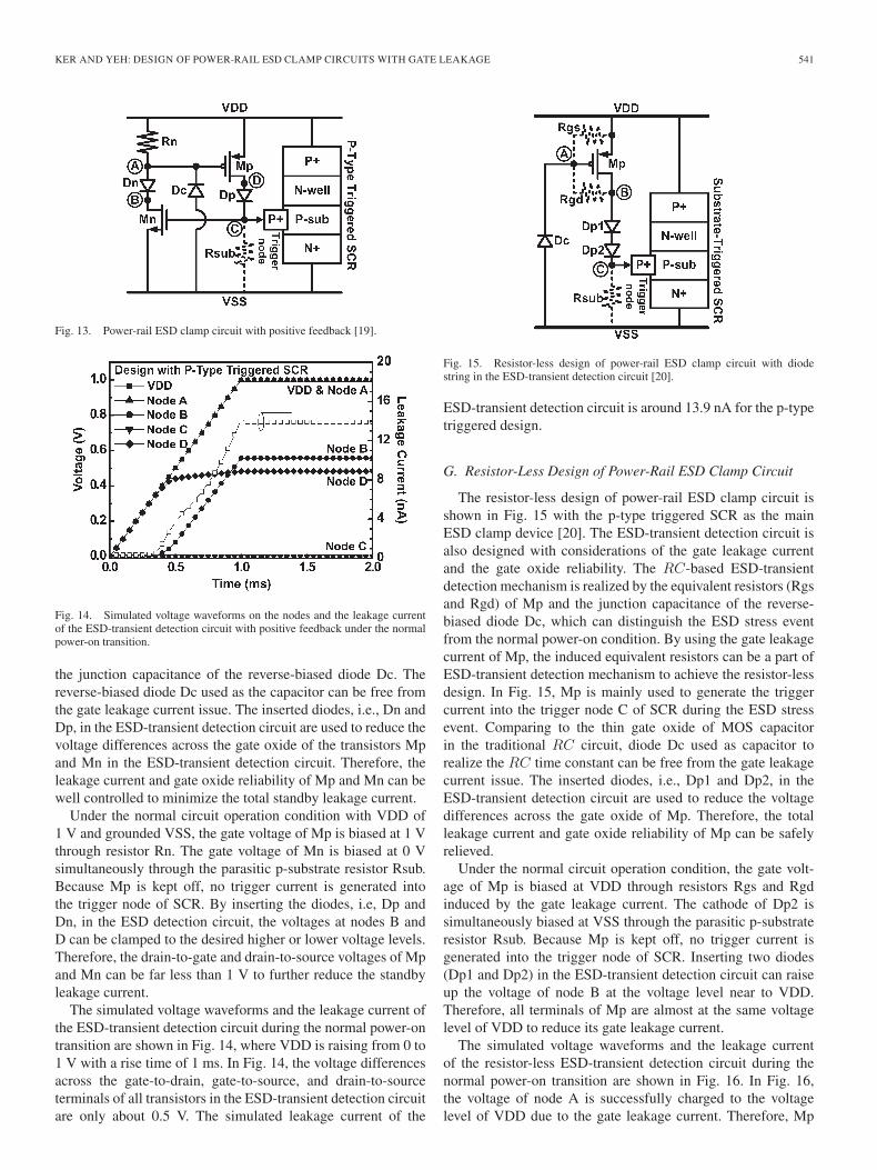
The modified power-rail ESD clamp circuit with p-typetriggered SCR as the main ESD clamp device is shown inFig. 13 [19]. The ESD-transient detection circuit is designedwith considerations of the gate leakage current and the gateoxide reliability. In Fig. 13, Mp is used to generate the triggercurrent into the trigger node C of the p-type triggered SCRduring the ESD stress event. Under the normal circuit operatingcondition, Mp is kept off and the trigger node is kept at VSSthrough the parasitic p-substrate resistor Rsub. Therefore, thep-type triggered SCR device is turned off during the normalcircuit operating condition.
Due to lack of parasitic capacitor of BigFET, the RC-basedESD-transient detection mechanism is realized by the Rn and
KER AND YEH: DESIGN OF POWER-RAIL ESD CLAMP CIRCUITS WITH GATE LEAKAGE 541
Fig. 13. Power-rail ESD clamp circuit with positive feedback [19].
Fig. 14. Simulated voltage waveforms on the nodes and the leakage currentof the ESD-transient detection circuit with positive feedback under the normalpower-on transition.
the junction capacitance of the reverse-biased diode Dc. Thereverse-biased diode Dc used as the capacitor can be free fromthe gate leakage current issue. The inserted diodes, i.e., Dn andDp, in the ESD-transient detection circuit are used to reduce thevoltage differences across the gate oxide of the transistors Mpand Mn in the ESD-transient detection circuit. Therefore, theleakage current and gate oxide reliability of Mp and Mn can bewell controlled to minimize the total standby leakage current.
Under the normal circuit operation condition with VDD of1 V and grounded VSS, the gate voltage of Mp is biased at 1 Vthrough resistor Rn. The gate voltage of Mn is biased at 0 Vsimultaneously through the parasitic p-substrate resistor Rsub.Because Mp is kept off, no trigger current is generated intothe trigger node of SCR. By inserting the diodes, i.e, Dp andDn, in the ESD detection circuit, the voltages at nodes B andD can be clamped to the desired higher or lower voltage levels.Therefore, the drain-to-gate and drain-to-source voltages of Mpand Mn can be far less than 1 V to further reduce the standbyleakage current.
The simulated voltage waveforms and the leakage current ofthe ESD-transient detection circuit during the normal power-ontransition are shown in Fig. 14, where VDD is raising from 0 to1 V with a rise time of 1 ms. In Fig. 14, the voltage differencesacross the gate-to-drain, gate-to-source, and drain-to-sourceterminals of all transistors in the ESD-transient detection circuitare only about 0.5 V. The simulated leakage current of the
Fig. 15. Resistor-less design of power-rail ESD clamp circuit with diodestring in the ESD-transient detection circuit [20].
ESD-transient detection circuit is around 13.9 nA for the p-typetriggered design.
G. Resistor-Less Design of Power-Rail ESD Clamp Circuit
The resistor-less design of power-rail ESD clamp circuit isshown in Fig. 15 with the p-type triggered SCR as the mainESD clamp device [20]. The ESD-transient detection circuit isalso designed with considerations of the gate leakage currentand the gate oxide reliability. The RC-based ESD-transientdetection mechanism is realized by the equivalent resistors (Rgsand Rgd) of Mp and the junction capacitance of the reverse-biased diode Dc, which can distinguish the ESD stress eventfrom the normal power-on condition. By using the gate leakagecurrent of Mp, the induced equivalent resistors can be a part ofESD-transient detection mechanism to achieve the resistor-lessdesign. In Fig. 15, Mp is mainly used to generate the triggercurrent into the trigger node C of SCR during the ESD stressevent. Comparing to the thin gate oxide of MOS capacitorin the traditional RC circuit, diode Dc used as capacitor torealize the RC time constant can be free from the gate leakagecurrent issue. The inserted diodes, i.e., Dp1 and Dp2, in theESD-transient detection circuit are used to reduce the voltagedifferences across the gate oxide of Mp. Therefore, the totalleakage current and gate oxide reliability of Mp can be safelyrelieved.
Under the normal circuit operation condition, the gate volt-age of Mp is biased at VDD through resistors Rgs and Rgdinduced by the gate leakage current. The cathode of Dp2 issimultaneously biased at VSS through the parasitic p-substrateresistor Rsub. Because Mp is kept off, no trigger current isgenerated into the trigger node of SCR. Inserting two diodes(Dp1 and Dp2) in the ESD-transient detection circuit can raiseup the voltage of node B at the voltage level near to VDD.Therefore, all terminals of Mp are almost at the same voltagelevel of VDD to reduce its gate leakage current.
The simulated voltage waveforms and the leakage currentof the resistor-less ESD-transient detection circuit during thenormal power-on transition are shown in Fig. 16. In Fig. 16,the voltage of node A is successfully charged to the voltagelevel of VDD due to the gate leakage current. Therefore, Mp

542 IEEE TRANSACTIONS ON DEVICE AND MATERIALS RELIABILITY, VOL. 14, NO. 1, MARCH 2014
Fig. 16. Simulated voltage waveforms on the nodes and the leakage currentof the resistor-less ESD-transient detection circuit under the normal power-ontransition.
Fig. 17. Power-rail ESD clamp circuit with diode-string ESD detection [21].
is completely turned off, and the simulated standby leakagecurrent of the ESD-transient detection circuit is only 1.53 nA.
H. Diode-String ESD Detection Circuit
The power-rail ESD clamp circuit designed with diode-stringESD detection is shown in Fig. 17 with the p-type triggeredSCR as the main ESD clamp device [21]. This design wasimplemented with a diode string and a resistor to detect the ESDevents by the high voltage level instead of the fast rise time.
Under normal circuit operation, the VDD operating voltage islower than the diode string threshold voltage. Therefore, thereis no current flowing through R, and Mp is kept off. Addinga voltage drop by using a diode Do between Mp drain andthe SCR trigger point (VTRIG) would effectively reduce theleakage current from Mp. Under a PS ESD stress, the diodestring starts to conduct some current when the VDD voltageoverpasses the diode string threshold voltage. That causes avoltage drop across R, thus turning Mp on to trigger the SCR.
The simulated results of this design with diode-string ESDdetection during the normal power-on transition are shown inFig. 18. In Fig. 18, the voltage (VA) of node A is successfullycharged to the voltage level of VDD. Therefore, Mp is com-pletely turned off and the simulated standby leakage current isonly 52 nA.
Fig. 18. Simulated voltage waveforms on the nodes and the leakage currentof the diode-string ESD detection circuit under the normal power-on transition.
IV. DISCUSSION AND COMPARISON
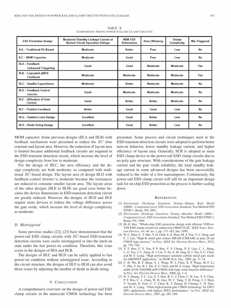
The comparison among various power-rail ESD clamp cir-cuits is summarized in Table II. Some evaluated parameters areexplained as the following.
A. Standby Leakage Current
For the standby leakage current, the designs of II.A andII.C are moderate. For the design of II.C, although the MOScapacitor is replaced by MOM capacitor, the voltage differenceacross the transistors of inverter is not sufficiently reduced.By carefully considering the voltage difference across the gateoxide, the standby leakage current of the other designs (III.Dto III.H) can be greatly reduced. In particular, for the designof III.G, the measured standby leakage current is only a fewnanoamperes because all terminals of the MOSFET are biasedat the same voltage level of VDD.
B. HBM ESD Robustness
In the design of III.B, the HBM ESD robustness is moderatefor over 3 kV. With over 2000 μm channel width of ESD clampdevice, the HBM ESD robustness of design III.A is good to beover 5 kV. For the designs of II.A and III.C, the HBM ESDrobustness is better due to over 8 kV.
In designs of II.C, III.F, and III.G, the HBM ESD robustnessis good for over 4 kV and 5 kV, respectively. With 120 μmSCR width in the design of III.D, the HBM ESD robustness ismoderate to over 8 kV. However, the HBM ESD level of designIII.E (III.H) is better to be 7 kV (6.5 kV) with only 45 μm(40 μm) SCR width.
C. Area Efficiency and Design Complexity
The area efficiency of traditional RC-based design (II.A)is poor because the RC time constant is typically designedabout 0.1–1 μs. It would consume large layout area to im-plement resistor and capacitor, but the design complexity oftraditional RC-based design is low. The layout area of designII.C with MOM capacitor is poor because the ESD-transientdetection circuit is based on traditional RC-based design andstill consumes large layout area to implement resistor and
KER AND YEH: DESIGN OF POWER-RAIL ESD CLAMP CIRCUITS WITH GATE LEAKAGE 543
TABLE IICOMPARISON AMONG POWER FAILURE CLAMP CIRCUITS
MOM capacitor. Some previous designs (III.A and III.B) withfeedback mechanism were presented to reduce the RC timeconstant and layout area. However, the reduction of layout areais limited because additional feedback circuits are required inthe ESD-transient detection circuit, which increase the level ofdesign complexity from low to moderate.
For the design of III.C, the area efficiency and the de-sign complexity are both moderate, as compared with tradi-tional RC-based design. The layout area of design III.D withfeedback-control inverter is moderate because the resistancesare reduced to consume smaller layout area. The layout areasof the other designs (III.E to III.H) are good even better be-cause the device dimensions in ESD-transient detection circuitare greatly reduced. However, the designs of III.D and III.Erequire more devices to reduce the voltage difference acrossthe gate oxide, which increase the level of design complexityas moderate.
D. Mistriggered
Some previous studies [22], [23] have demonstrated that thepower-rail ESD clamp circuits with RC-based ESD-transientdetection circuits were easily mistriggered or into the latch-onstate under the fast power-on condition. Therefore, this issueexists in the designs of IIIA and III.B.
The designs of III.C and III.D can be safely applied to fastpower-on condition without mistriggered issue. According tothe circuit structure, the designs of III.F to III.H can also avoidthose issues by adjusting the number of diode in diode string.
V. CONCLUSION
A comprehensive overview on the design of power-rail ESDclamp circuits in the nanoscale CMOS technology has been
presented. Some process and circuit techniques used in theESD-transient detection circuits were adopted to perform betterturn-on behavior, lower standby leakage current, and higherefficiency of layout area. Generally, SCR is adopted as mainESD clamp device in the power-rail ESD clamp circuits due tono poly-gate structure. With considerations of the gate leakagecurrent and the gate oxide reliability, the total standby leak-age current in some advanced designs has been successfullyreduced to the order of a few nanoamperes. Continuously, thepower-rail ESD clamp circuit will still be an important designtask for on-chip ESD protection as the process is further scalingdown.
REFERENCES
[1] Electrostatic Discharge Sensitivity Testing—Human Body Model(HBM)—Component Level, ESD Association Standard, Test Method ESDSTM5.1, Rome, NY, 2001.
[2] Electrostatic Discharge Sensitivity Testing—Machine Model (MM)—Component Level, ESD Association Standard, Test Method ESD STM5.2,Rome, NY, 1999.
[3] M.-D. Ker, “Whole-chip ESD protection design with efficient VDD-to-VSS ESD clamp circuits for submicron CMOS VLSI,” IEEE Trans. Elec-tron Devices, vol. 46, no. 1, pp. 173–183, Jan. 1999.
[4] W. C. Shen, C. Y. Mei, Y.-D. Chih, S.-S. Sheu, M.-J. Tsai, Y.-C. King, andC. J. Lin, “High-K metal gate contact RRAM (CRRAM) in pure 28 nmCMOS logic process,” in Proc. IEEE Int. Electron Devices Meet., 2012,pp. 745–748.
[5] Y. T. Hou, F. Y. Yen, P. F. Hsu, V. S. Chang, P. S. Lim, C. L. Hung,L. G. Yao, J. C. Jiang, H. J. Lin, Y. Jin, S. M. Jang, H. J. Tao, S. C. Chen,and M. S. Liang, “High performance tantalum carbide metal gate stacksfor nMOSFET application,” in IEDM Tech. Dig., 2005, pp. 31–34.
[6] C. H. Wu, B. F. Hung, S. J. Wang, W. J. Chen, X. P. Wang, M.-F. Li,C. Zhu, Y. Jin, H. J. Tao, S. C. Chen, and M. S. Liang, “High temperaturestable [Ir3Si-TaN]/HfLaON CMOS with large work-function difference,”in Proc. Int. Electron Devices Meet., 2006, pp. 1–4.
[7] H. T. Huang, Y. C. Liu, Y. T. Hou, R. C.-J. Chen, C. H. Lee, Y. S. Chao,P. F. Hsu, C. L. Chen, W. H. Guo, W. C. Yang, T. H. Perng, J. J. Shen,Y. Yasuda, K. Goto, C. C. Chen, K. T. Huang, H. Chuang, C. H. Diaz,and M. S. Liang, “45nm high-k/metal-gate CMOS technology for GPU/NPU applications with highest PFET performance,” in Proc. IEEE Int.Electron Devices Meet., 2007, pp. 285–288.
544 IEEE TRANSACTIONS ON DEVICE AND MATERIALS RELIABILITY, VOL. 14, NO. 1, MARCH 2014
[8] C. H. Diaz, K. Goto, H. T. Huang, Yu. Yasuda, C. P. Tsao, T. T. Chu,W. T. Lu, V. Chang, Y. T. Hou, Y. S. Chao, P. F. Hsu, C. L. Chen,K. C. Lin, J. A. Ng, W. C. Yang, C. H. Chen, Y. H. Peng, C. J. Chen,C. C. Chen, M. H. Yu, L. Y. Yeh, K. S. You, K. S. Chen, K. B. Thei,C. H. Lee, S. H. Yang, J. Y. Cheng, K. T. Huang, J. J. Liaw, Y. Ku,S. M. Jang, H. Chuang, and M. S. Liang, “32 nm gate-first high-k/metal-gate technology for high performance low power applications,” in Proc.IEEE Int. Electron Devices Meet., 2008, pp. 1–4.
[9] H. Samavati, A. Hajimiri, A. Shahani, G. Nasserbakht, and T. Lee,“Fractal capacitors,” IEEE J. Solid-State Circuits, vol. 33, no. 12,pp. 2035–2041, Dec. 1998.
[10] P.-Y. Chiu and M.-D. Ker, “Design of low-leakage power-rail ESD clampcircuit with MOM capacitor and STSCR in a 65-nm CMOS process,” inProc. IEEE Int. Conf. Integr. Circuit Design Technol., 2011, pp. 1–4.
[11] M.-D. Ker and K.-C. Hsu, “Overview of on-chip electrostatic dischargeprotection design with SCR-based devices in CMOS integrated circuits,”IEEE Trans. Device Mater. Rel., vol. 5, no. 2, pp. 235–249, Jun. 2005.
[12] J. C. Smith and G. Boselli, “A MOSFET power supply clamp withfeedback enhanced triggering for ESD protection in advanced CMOStechnologies,” in Proc. EOS/ESD Symp., 2003, pp. 8–16.
[13] J. Li, R. Gauthier, and E. Rosenbaum, “A compact, timed-shutoff,MOSFET-based power clamp for on-chip ESD protection,” in Proc.EOS/ESD Symp., 2004, pp. 273–279.
[14] S.-H. Chen and M.-D. Ker, “Area-efficient ESD-transient detection circuitwith smaller capacitance for on-chip power-rail ESD protection in CMOSICs,” IEEE Trans. Circuits Syst. II, Exp. Briefs, vol. 56, no. 5, pp. 359–363, May 2009.
[15] BSIM Model, Berkeley Short-Channel IGFET Model. [Online]. Available:http://www-device.eecs.berkeley.edu/bsim
[16] M.-D. Ker and P.-Y. Chiu, “New low-leakage power-rail ESD clamp cir-cuit in a 65-nm low-voltage CMOS process,” IEEE Trans. Device Mater.Rel., vol. 11, no. 3, pp. 474–483, Sep. 2011.
[17] C.-T. Wang and M.-D. Ker, “Design of power-rail ESD clamp circuit withultra-low standby leakage current in nanoscale CMOS technology,” IEEEJ. Solid-State Circuits, vol. 44, no. 3, pp. 956–964, Mar. 2009.
[18] C.-T. Yeh and M.-D. Ker, “Capacitor-less design of power-rail ESD clampcircuit with adjustable holding voltage for on-chip ESD protection,” IEEEJ. Solid-State Circuits, vol. 45, no. 11, pp. 2476–2486, Nov. 2010.
[19] C.-T. Yeh and M.-D. Ker, “Power-rail ESD clamp circuit with ultralowstandby leakage current and high area efficiency in nanometer CMOStechnology,” IEEE Trans. Electron Devices, vol. 59, no. 10, pp. 2626–2634, Oct. 2012.
[20] C.-T. Yeh and M.-D. Ker, “Resistor-less design of power-rail ESD clampcircuit in nanoscale CMOS technology,” IEEE Trans. Electron Devices,vol. 59, no. 12, pp. 3456–3463, Dec. 2012.
[21] F. A. Altolaguirre and M.-D. Ker, “Power-rail ESD clamp circuitwith diode-string ESD detection to overcome the gate leakage currentin a 40-nm CMOS process,” IEEE Trans. Electron Devices, vol. 60,no. 10, pp. 3500–3507, Oct. 2013.
[22] C.-C. Yen and M.-D. Ker, “The effect of IEC-like fast transients on RC-triggered ESD power clamps,” IEEE Trans. Electron Devices, vol. 56,no. 6, pp. 1204–1210, Jun. 2009.
[23] C.-T. Yeh and M.-D. Ker, “High area-efficient ESD clamp circuit withequivalent RC-based detection mechanism in a 65-nm CMOS process,”IEEE Trans. Electron Devices, vol. 60, no. 3, pp. 1011–1018, Mar. 2013.
Ming-Dou Ker (F’08) received the Ph.D. degreefrom the Institute of Electronics, National ChiaoTung University (NCTU), Hsinchu, Taiwan, in 1993.
He is currently the Distinguished Professor in theDepartment of Electronics Engineering; and also theDean of the College of Photonics in NCTU. He isalso serving as the Editor of IEEE TRANSACTIONS
ON DEVICE AND MATERIALS RELIABILITY.
Chih-Ting Yeh (M’13) received the Ph.D. degreefrom the Institute of Electronics, National ChiaoTung University, Hsinchu, Taiwan, in 2013.
He is with Industrial Technology Research Insti-tute, Hsinchu.